A silicon-nanowire memory driven by optical gradient force induced bistability B. Dong, H. Cai, L. K. Chin, J. G. Huang, Z. C. Yang, Y. D. Gu, G. I. Ng, W. Ser, D. L. Kwong, and A. Q. Liu Citation: Applied Physics Letters 107, 261111 (2015); doi: 10.1063/1.4939114 View online: http://dx.doi.org/10.1063/1.4939114 View Table of Contents: http://scitation.aip.org/content/aip/journal/apl/107/26?ver=pdfcov Published by the AIP Publishing Articles you may be interested in Optical absorption of silicon nanowires J. Appl. Phys. 112, 033506 (2012); 10.1063/1.4739708 Optical bistability in mesoporous silicon microcavity resonators J. Appl. Phys. 109, 093113 (2011); 10.1063/1.3585782 Optical memory of silicon nanocrystals with submicron spatial resolution and very high thermal stability Appl. Phys. Lett. 94, 173116 (2009); 10.1063/1.3127228 Ga ∕ Au alloy catalyst for single crystal silicon-nanowire epitaxy Appl. Phys. Lett. 90, 023109 (2007); 10.1063/1.2431468 Silicon optical nanocrystal memory Appl. Phys. Lett. 85, 2622 (2004); 10.1063/1.1795364 This article is copyrighted as indicated in the article. Reuse of AIP content is subject to the terms at: http://scitation.aip.org/termsconditions. Downloaded to IP: 155.69.4.4 On: Thu, 31 Dec 2015 02:31:17
Transcript
A silicon-nanowire memory driven by optical gradient force induced bistabilityB. Dong, H. Cai, L. K. Chin, J. G. Huang, Z. C. Yang, Y. D. Gu, G. I. Ng, W. Ser, D. L. Kwong, and A. Q. Liu Citation: Applied Physics Letters 107, 261111 (2015); doi: 10.1063/1.4939114 View online: http://dx.doi.org/10.1063/1.4939114 View Table of Contents: http://scitation.aip.org/content/aip/journal/apl/107/26?ver=pdfcov Published by the AIP Publishing Articles you may be interested in Optical absorption of silicon nanowires J. Appl. Phys. 112, 033506 (2012); 10.1063/1.4739708 Optical bistability in mesoporous silicon microcavity resonators J. Appl. Phys. 109, 093113 (2011); 10.1063/1.3585782 Optical memory of silicon nanocrystals with submicron spatial resolution and very high thermal stability Appl. Phys. Lett. 94, 173116 (2009); 10.1063/1.3127228 Ga ∕ Au alloy catalyst for single crystal silicon-nanowire epitaxy Appl. Phys. Lett. 90, 023109 (2007); 10.1063/1.2431468 Silicon optical nanocrystal memory Appl. Phys. Lett. 85, 2622 (2004); 10.1063/1.1795364
This article is copyrighted as indicated in the article. Reuse of AIP content is subject to the terms at: http://scitation.aip.org/termsconditions. Downloaded to IP: 155.69.4.4
A silicon-nanowire memory driven by optical gradient force inducedbistability
B. Dong,1,2 H. Cai,2,a) L. K. Chin,1 J. G. Huang,1,2,3 Z. C. Yang,4 Y. D. Gu,2 G. I. Ng,1
W. Ser,1 D. L. Kwong,2 and A. Q. Liu1,4,b)
1School of Electrical and Electronic Engineering, Nanyang Technological University, Singapore 6397982Institute of Microelectronics, A*STAR (Agency for Science, Technology and Research), Singapore 1176853School of Mechanical Engineering, Xi’an Jiaotong University, Xi’an 710049, China4School of Electronics Engineering and Computer Science, Peking University, Beijing 100871, China
(Received 21 October 2015; accepted 15 December 2015; published online 30 December 2015)
In this paper, a bistable optical-driven silicon-nanowire memory is demonstrated, which employs
ring resonator to generate optical gradient force over a doubly clamped silicon-nanowire. Two
stable deformation positions of a doubly clamped silicon-nanowire represent two memory states
(“0” and “1”) and can be set/reset by modulating the light intensity (<3 mW) based on the optical
force induced bistability. The time response of the optical-driven memory is less than 250 ns. It has
applications in the fields of all optical communication, quantum computing, and optomechanical
This article is copyrighted as indicated in the article. Reuse of AIP content is subject to the terms at: http://scitation.aip.org/termsconditions. Downloaded to IP: 155.69.4.4
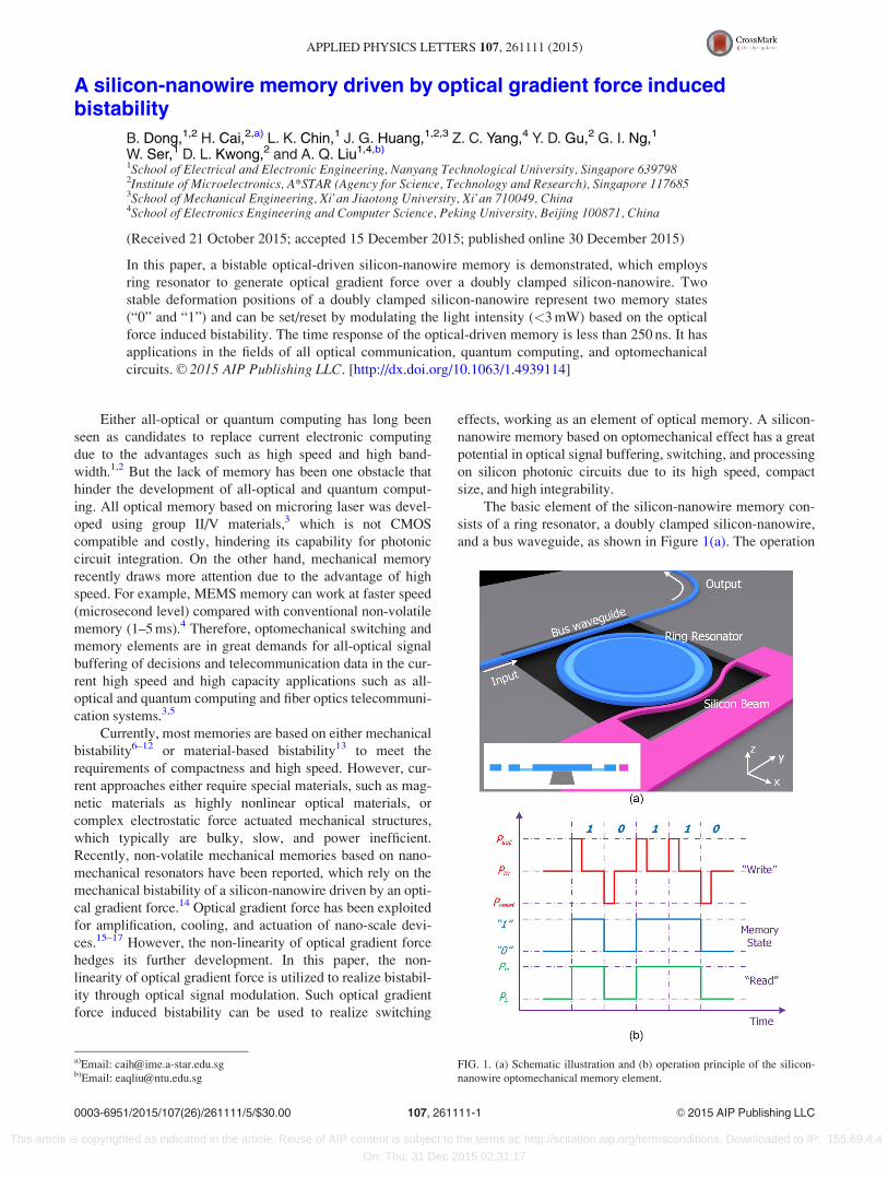
of the silicon-nanowire memory element requires two lights
to realize the write and read processes, named WRITE (W)
light and READ (R) light. The W light is coupled from the
bus waveguide into the ring resonator and the optical gradi-
ent force is thereafter initiated between the ring resonator
and the silicon nanowire. Such force pulls the silicon nano-
wire towards the ring resonator. The silicon nanowire has
two stable positions owing to the nonlinearity of the optical
gradient force, which are identified as memory states. These
memory states are thereafter identified as different intensity
levels of the R light. The operation of the optomechanical
memory is summarized in Figure 1(b). The W light can set
the memory to “1” with a high power pulse (Pset) with the
transmission of the R light being kept at high power level
(PH). Otherwise, the W light can reset the memory to “0”
with the notch in power (Preset) such that the transmission of
the R light is kept at low power level (PL).
The wavelength of W light kW is red detuned as com-
pared with the resonance wavelength of the ring resonator
and the wavelength detuning is defined as
d ¼ kW � kð0Þ; (1)
where kð0Þ is the resonance wavelength of the ring resonator
at zero deformation. The resonance wavelength of ring reso-
nator depends on the geometry of the ring resonator, which
is defined as
k ¼ 2pnef f R
N; (2)
where R is the radius of the ring resonator and N is an inte-
gral number. The effective refractive index neff describes the
light propagation properties in waveguides and can be simu-
lated by using Lumerical. The generated optical gradient
force by W light can be expressed as18
Foptical xð Þ ¼ � 2cePoptical
nef f xð Þgom xð Þ
D xð Þ2 þ c2; (3)
where ce is the external damping due to waveguide-ring cou-
pling, Poptical is the light power, gom(x) is the optomechanical
coupling coefficient, c is the total damping coefficient, and
D(x) is the laser detuning that is defined as
D xð Þ ¼ x xð Þ � xW ¼ 2pc1
k xð Þ� 1
kW
� �; (4)
where k(x) is the resonance wavelength of the ring resonator
at x deformation of the silicon nanowire.
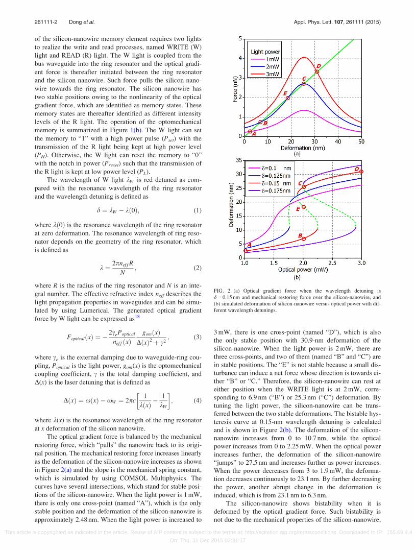
The optical gradient force is balanced by the mechanical
restoring force, which “pulls” the nanowire back to its origi-
nal position. The mechanical restoring force increases linearly
as the deformation of the silicon-nanowire increases as shown
in Figure 2(a) and the slope is the mechanical spring constant,
which is simulated by using COMSOL Multiphysics. The
curves have several intersections, which stand for stable posi-
tions of the silicon-nanowire. When the light power is 1 mW,
there is only one cross-point (named “A”), which is the only
stable position and the deformation of the silicon-nanowire is
approximately 2.48 nm. When the light power is increased to
3 mW, there is one cross-point (named “D”), which is also
the only stable position with 30.9-nm deformation of the
silicon-nanowire. When the light power is 2 mW, there are
three cross-points, and two of them (named “B” and “C”) are
in stable positions. The “E” is not stable because a small dis-
turbance can induce a net force whose direction is towards ei-
ther “B” or “C.” Therefore, the silicon-nanowire can rest at
either position when the WRITE light is at 2 mW, corre-
sponding to 6.9 nm (“B”) or 25.3 nm (“C”) deformation. By
tuning the light power, the silicon-nanowire can be trans-
ferred between the two stable deformations. The bistable hys-
teresis curve at 0.15-nm wavelength detuning is calculated
and is shown in Figure 2(b). The deformation of the silicon-
nanowire increases from 0 to 10.7 nm, while the optical
power increases from 0 to 2.25 mW. When the optical power
increases further, the deformation of the silicon-nanowire
“jumps” to 27.5 nm and increases further as power increases.
When the power decreases from 3 to 1.9 mW, the deforma-
tion decreases continuously to 23.1 nm. By further decreasing
the power, another abrupt change in the deformation is
induced, which is from 23.1 nm to 6.3 nm.
The silicon-nanowire shows bistability when it is
deformed by the optical gradient force. Such bistability is
not due to the mechanical properties of the silicon-nanowire,
FIG. 2. (a) Optical gradient force when the wavelength detuning is
d¼ 0.15 nm and mechanical restoring force over the silicon-nanowire, and
(b) simulated deformation of silicon-nanowire versus optical power with dif-
ferent wavelength detunings.
261111-2 Dong et al. Appl. Phys. Lett. 107, 261111 (2015)
This article is copyrighted as indicated in the article. Reuse of AIP content is subject to the terms at: http://scitation.aip.org/termsconditions. Downloaded to IP: 155.69.4.4
On: Thu, 31 Dec 2015 02:31:17
but can be manipulated by controlling the wavelength and
power of the W light, as shown in Figure 2(b). The silicon-
nanowire is deformed in different paths based on different
wavelength detunings. When the wavelength detuning is
0.1 nm, the silicon-nanowire shows only one stable position
at all times and therefore no bistability. When the wavelength
detuning is increased to 0.125 nm, there is only a very narrow
region where the silicon-nanowire shows two stable positions
and the transition curve is close to a vertical line. This is the
critical condition where the silicon-nanowire starts to show
bistability. When the wavelength detuning is increased to
0.175 nm, the bistable region is further broadened. Therefore,
both the power and wavelength of write light are critical to
control the bistability of the silicon-nanowire.
The deformations of the silicon-nanowire are sensed by
the R light. Initially, the wavelength of the R light matches
with another resonance wavelength of the ring resonator,
causing a low power level (PL) at output. When the power of
the W light is increased, the optical gradient force is increased
and the silicon-nanowire moves towards the ring resonator.
The deformation of the silicon-nanowire results in the change
in the effective refractive index Dneff of the ring resonator,
causing a red shift of the ring resonance wavelength Dkr. The
R light can be transmitted through the waveguide, causing a
high power level (PH) at output, since its wavelength is no
longer matched with the resonance wavelength now.
Therefore, the transmission of the R light can be controlled by
pumping a red-detuned W light powered at different levels.
The memory elements are connected together by the bus
waveguides to form the memory array. Each element can be
written and read individually by differentiating the resonance
wavelength of each element. A 4� 4 memory array, which
integrates 16 memory elements, is fabricated by nano-silicon-
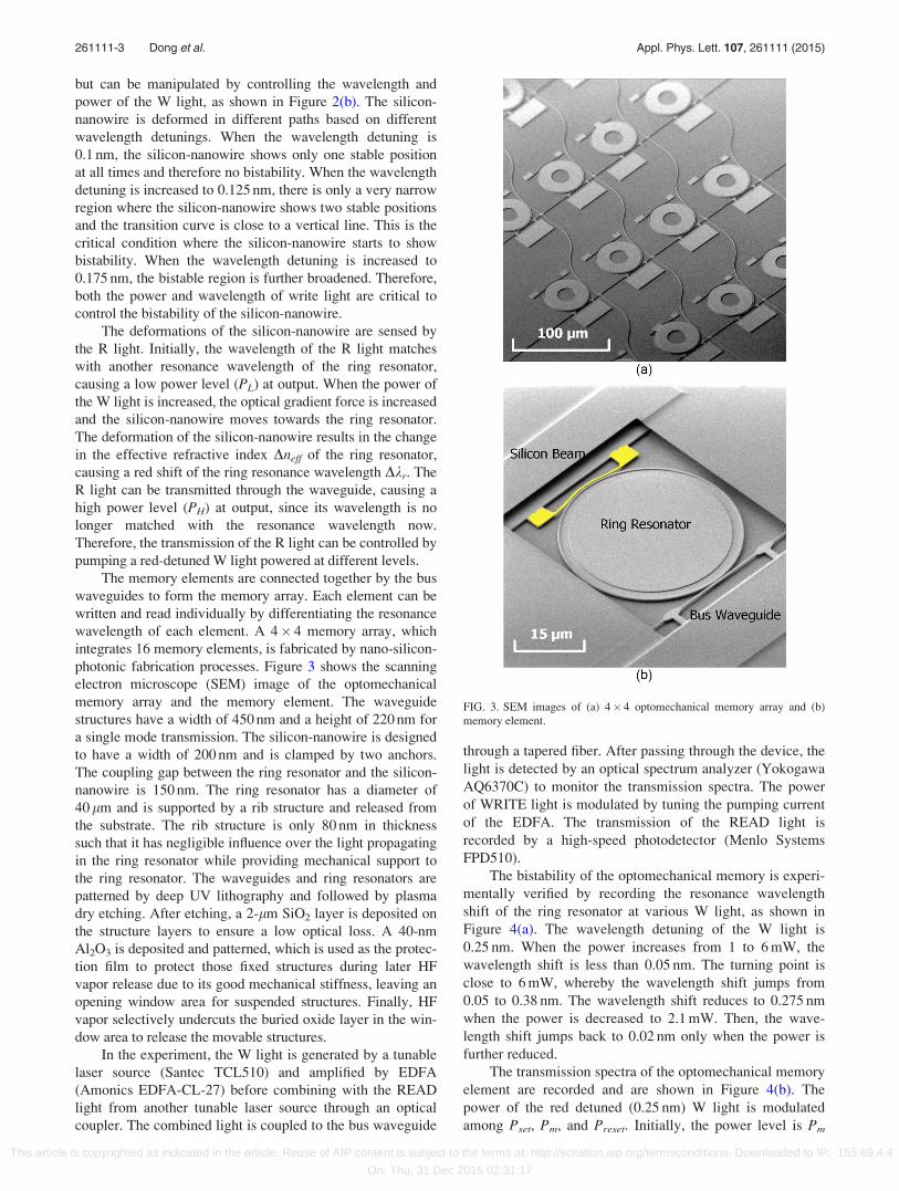
photonic fabrication processes. Figure 3 shows the scanning
electron microscope (SEM) image of the optomechanical
memory array and the memory element. The waveguide
structures have a width of 450 nm and a height of 220 nm for
a single mode transmission. The silicon-nanowire is designed
to have a width of 200 nm and is clamped by two anchors.
The coupling gap between the ring resonator and the silicon-
nanowire is 150 nm. The ring resonator has a diameter of
40 lm and is supported by a rib structure and released from
the substrate. The rib structure is only 80 nm in thickness
such that it has negligible influence over the light propagating
in the ring resonator while providing mechanical support to
the ring resonator. The waveguides and ring resonators are
patterned by deep UV lithography and followed by plasma
dry etching. After etching, a 2-lm SiO2 layer is deposited on
the structure layers to ensure a low optical loss. A 40-nm
Al2O3 is deposited and patterned, which is used as the protec-
tion film to protect those fixed structures during later HF
vapor release due to its good mechanical stiffness, leaving an
opening window area for suspended structures. Finally, HF
vapor selectively undercuts the buried oxide layer in the win-
dow area to release the movable structures.
In the experiment, the W light is generated by a tunable
laser source (Santec TCL510) and amplified by EDFA
(Amonics EDFA-CL-27) before combining with the READ
light from another tunable laser source through an optical
coupler. The combined light is coupled to the bus waveguide
through a tapered fiber. After passing through the device, the
light is detected by an optical spectrum analyzer (Yokogawa
AQ6370C) to monitor the transmission spectra. The power
of WRITE light is modulated by tuning the pumping current
of the EDFA. The transmission of the READ light is
recorded by a high-speed photodetector (Menlo Systems
FPD510).
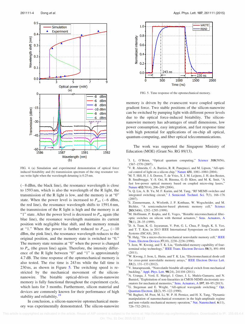
The bistability of the optomechanical memory is experi-
mentally verified by recording the resonance wavelength
shift of the ring resonator at various W light, as shown in
Figure 4(a). The wavelength detuning of the W light is
0.25 nm. When the power increases from 1 to 6 mW, the
wavelength shift is less than 0.05 nm. The turning point is
close to 6 mW, whereby the wavelength shift jumps from
0.05 to 0.38 nm. The wavelength shift reduces to 0.275 nm
when the power is decreased to 2.1 mW. Then, the wave-
length shift jumps back to 0.02 nm only when the power is
further reduced.
The transmission spectra of the optomechanical memory
element are recorded and are shown in Figure 4(b). The
power of the red detuned (0.25 nm) W light is modulated
among Pset, Pm, and Preset. Initially, the power level is Pm
FIG. 3. SEM images of (a) 4� 4 optomechanical memory array and (b)
memory element.
261111-3 Dong et al. Appl. Phys. Lett. 107, 261111 (2015)
This article is copyrighted as indicated in the article. Reuse of AIP content is subject to the terms at: http://scitation.aip.org/termsconditions. Downloaded to IP: 155.69.4.4
On: Thu, 31 Dec 2015 02:31:17
(�8 dBm, the black line), the resonance wavelength is close
to 1593 nm, which is also the wavelength of the R light, the
transmission of the R light is low, and the memory is at “0”
state. When the power level is increased to Pset (�6 dBm,
the red line), the resonance wavelength shifts to 1591.6 nm,
the transmission of the R light is high and the memory is at
“1” state. After the power level is decreased to Pm again (the
blue line), the resonance wavelength maintains its current
position with negligible blue shift, and the memory remain
at “1.” When the power is further reduced to Preset (�10
dBm, the pink line), the resonance wavelength reduces to the
original position, and the memory state is switched to “0.”
The memory state remains at “0” when the power is changed
to Pm (the green line) again. Therefore, the intensity differ-
ence of the R light between “0” and “1” is approximately
4.7 dB. The time response of the optomechanical memory is
also tested. The rise time is 243 ns while the fall time is
230 ns, as shown in Figure 5. The switching speed is re-
stricted by the mechanical movement of the silicon-
nanowire. The bistable optical-driven silicon-nanowire
memory is fully functional throughout the experiment cycle,
which lasts for 3 months. Furthermore, silicon material and
devices are commonly known for their performance of high
stability and reliability.19
In conclusion, a silicon-nanowire optomechanical mem-
ory was experimentally demonstrated. The silicon-nanowire
memory is driven by the evanescent wave coupled optical
gradient force. Two stable positions of the silicon-nanowire
can be switched by pumping light with different power levels
due to the optical force-induced bistability. The silicon-
nanowire memory has advantages of small dimensions, low
power consumption, easy integration, and fast response time
with high potential for applications of on-chip all optical,
quantum-computing, and fiber optical telecommunications.
The work was supported the Singapore Ministry of
Education (MOE) (Grant No. RG 89/13).
1J. L. O’Brien, “Optical quantum computing,” Science 318(5856),
1567–1570 (2007).2V. R. Almeida, C. A. Barrios, R. R. Panepucci, and M. Lipson, “All-opti-
cal control of light on a silicon chip,” Nature 431, 1081–1084 (2004).3M. T. Hill, H. J. S. Dorren, T. de Vries, X. J. M. Leijtens, J. H. den Besten,
B. Smalbrugge, Y.-S. Oei, H. Binsma, G.-D. Khoe, and M. K. Smit, “A
fast low-power optical memory based on coupled micro-ring lasers,”
Nature 432(7014), 206–209 (2004).4A. Q. Liu, A. B. Yu, M. F. Karim, and M. Tang, “RF MEMS switches and
integrated switching circuit,” J. Semicond. Technol. Sci. 7(3), 166–176
(2007).5S. Zimmermann, A. Wixforth, J. P. Kotthaus, W. Wegscheider, and M.
283(5406), 1292–1295 (1999).6M. Hoffmann, P. Kopka, and E. Voges, “Bistable micromechanical fibre-
optic switches on silicon with thermal actuators,” Sens. Actuators, A
78(1), 28–35 (1999).7D. A. Tuan, K. G. Jayaraman, V. Pott, G. L. Chua, P. Singh, K. S. Yeo,
and T. T. Kim, in 2013 IEEE International Symposium on Circuits and
Systems (ISCAS), 2013.8B. Halg, “On a micro-electro-mechanical nonvolatile memory cell,” IEEE
Trans. Electron Devices 37(10), 2230–2236 (1990).9J. Jeon, W. Kwong, and T. K. Liu, “Embedded memory capability of four-
terminal relay technology,” IEEE Trans. Electron Devices 58(3), 891–894
(2011).10W. Kwong, J. Jeon, L. Hutin, and T. K. Liu, “Electromechanical diode cell
for cross-point nonvolatile memory arrays,” IEEE Electron Device Lett.
33(2), 131–133 (2012).11V. Intaraprasonk, “Nonvolatile bistable all-optical switch from mechanical
buckling,” Appl. Phys. Lett. 98(24), 241104 (2011).12A. Uranga, J. Verd, E. Marig�o, J. Giner, J. L. Mu~n�oz-Gamarra, and N.
Barniol, “Exploitation of non-linearities in CMOS-NEMS electrostatic res-
onators for mechanical memories,” Sens. Actuators, A 197, 88–95 (2013).13G. Stegeman and E. Wright, “All-optical waveguide switching,” Opt.
Quantum Electron. 22(2), 95–122 (1990).14M. Bagheri, M. Poot, M. Li, W. P. H. Pernice, and H. X. Tang, “Dynamic
manipulation of nanomechanical resonators in the high-amplitude regime
and non-volatile mechanical memory operation,” Nat. Nanotechnol. 6(11),
726–732 (2011).
FIG. 4. (a) Simulation and experimental demonstration of optical force
induced bistability and (b) transmission spectrum of the ring resonator ver-
sus write light when the wavelength detuning is 0.25 nm.
FIG. 5. Time response of the optomechanical memory.
261111-4 Dong et al. Appl. Phys. Lett. 107, 261111 (2015)
This article is copyrighted as indicated in the article. Reuse of AIP content is subject to the terms at: http://scitation.aip.org/termsconditions. Downloaded to IP: 155.69.4.4
15H. Cai, K. J. Xu, A. Q. Liu, Q. Fang, M. B. Yu, G. Q. Lo, and D. L.
Kwong, “Nano-opto-mechanical actuator driven by gradient optical
force,” Appl. Phys. Lett. 100, 013108 (2012).16T. J. Kippenberg and K. J. Vahala, “Cavity optomechanics: Back-action at
the mesoscale,” Science 321(5893), 1172–1176 (2008).17B. Dong, H. Cai, G. I. Ng, P. Kropelnicki, J. M. Tsai, A. B. Randles, M.
Tang, Y. D. Gu, Z. G. Suo, and A. Q. Liu, “A nanoelectromechanical
systems actuator driven and controlled by Q-factor attenuation of ring res-
onator,” Appl. Phys. Lett. 103, 181105 (2013).18M. Ren, J. Huang, H. Cai, J. M. Tsai, J. Zhou, Z. Liu, Z. Suo, and A. Q.
Liu, “Nano-optomechanical actuator and pull-back instability,” ACS Nano
7(2), 1676–1681 (2013).19V. Lindroos, M. Tilli, A. Lehto, and T. Motooka, Handbook of Silicon Based
MEMS Materials and Technologies (William Andrew Publishing, 2010).
261111-5 Dong et al. Appl. Phys. Lett. 107, 261111 (2015)
This article is copyrighted as indicated in the article. Reuse of AIP content is subject to the terms at: http://scitation.aip.org/termsconditions. Downloaded to IP: 155.69.4.4