energies Article A Single-Phase Bidirectional AC/DC Converter for V2G Applications Tao Peng 1 , Peng Yang 1 , Hanbing Dan 1, * , Hui Wang 1 , Hua Han 1 , Jian Yang 1 , Hao Wang 1 , Hui Dong 1 and Patrick Wheeler 2 1 School of Information Science and Engineering, Central South University, Changsha 410083, China; [email protected] (T.P.);[email protected] (P.Y.);[email protected] (H.W.); [email protected] (H.H.); [email protected] (J.Y.); [email protected] (H.W.); [email protected] (H.D.) 2 Department of Electrical and Electronic Engineering, The University of Nottingham, Nottingham NG7 2RD, UK; [email protected]* Correspondence: [email protected]; Tel.: +44-074-21-876780 Received: 18 May 2017; Accepted: 26 June 2017; Published: 30 June 2017 Abstract: This paper presents a single-phase bidirectional current-source AC/DC converter for vehicle to grid (V2G) applications. The presented converter consists of a line frequency commutated unfolding bridge and an interleaved buck-boost stage. The low semiconductor losses of the line frequency commutated unfolding bridge contribute to the comparatively good efficiency of this converter. The buck and boost operating modes of the interleaved buck-boost stage provide operation over a wide battery voltage range. The interleaved structure of the interleaved buck-boost stage results in lower battery current ripple. In addition, sinusoidal input current, bidirectional power flow and reactive power compensation capability are also guaranteed. This paper presents the topology and operating principles of the presented converter. The feasibility of the converter is validated using MATLAB simulations, as well as experimental results. Keywords: bidirectional AC/DC converter; reactive power compensation capability; semiconductor losses; single-phase; V2G; wide battery voltage range 1. Introduction Currently, as the representative of the renewable energy vehicles, plug-in hybrid electric vehicles (PHEV) and electrical vehicles (EV) are beginning to play a major role in coping with energy shortages and environment pollution problems. Furthermore, EVs and PHEVs are also regarded as energy storage units, which could feed stored energy back to the grid when required. Vehicle-to-grid (V2G) technology is being used as the reference term for the two-way interaction between the electric vehicle and the grid [1,2]. EVs and PHEVs can offer a large number of advantages in this application, such as peak power regulating, peak load shifting, and non-loaded standby [3,4]. As an essential part of a V2G system, the battery charger can be used for bidirectional power flow with a sinusoidal input current and adjustable power factor. To prolong the life of the batteries, the battery charger should have low ripple of the battery current. The battery charger connects the grid to the vehicle or other DC load. As with household charging, the customers and developers are pursuing high efficiency and reliability at low cost. For V2G applications, the features of a battery charger, such as high power density, reactive power compensation capability, and low ripple of battery current, have become the focus of research attention [5,6]. In the past many different AC/DC converter topologies have been used as interfaces for EVs. A single-phase interleaved AC/DC boost converter for plug-in hybrid electric vehicles (PHEV) was proposed in [7], and other topologies that achieve the same functionality have been presented in [8]. Energies 2017, 10, 881; doi:10.3390/en10070881 www.mdpi.com/journal/energies
Transcript
energies
Article
A Single-Phase Bidirectional AC/DC Converter forV2G Applications
Tao Peng 1, Peng Yang 1 , Hanbing Dan 1,* , Hui Wang 1, Hua Han 1, Jian Yang 1, Hao Wang 1,Hui Dong 1 and Patrick Wheeler 2
Received: 18 May 2017; Accepted: 26 June 2017; Published: 30 June 2017
Abstract: This paper presents a single-phase bidirectional current-source AC/DC converter forvehicle to grid (V2G) applications. The presented converter consists of a line frequency commutatedunfolding bridge and an interleaved buck-boost stage. The low semiconductor losses of the linefrequency commutated unfolding bridge contribute to the comparatively good efficiency of thisconverter. The buck and boost operating modes of the interleaved buck-boost stage provide operationover a wide battery voltage range. The interleaved structure of the interleaved buck-boost stageresults in lower battery current ripple. In addition, sinusoidal input current, bidirectional power flowand reactive power compensation capability are also guaranteed. This paper presents the topologyand operating principles of the presented converter. The feasibility of the converter is validated usingMATLAB simulations, as well as experimental results.
Keywords: bidirectional AC/DC converter; reactive power compensation capability; semiconductorlosses; single-phase; V2G; wide battery voltage range
1. Introduction
Currently, as the representative of the renewable energy vehicles, plug-in hybrid electric vehicles(PHEV) and electrical vehicles (EV) are beginning to play a major role in coping with energy shortagesand environment pollution problems. Furthermore, EVs and PHEVs are also regarded as energystorage units, which could feed stored energy back to the grid when required. Vehicle-to-grid (V2G)technology is being used as the reference term for the two-way interaction between the electric vehicleand the grid [1,2]. EVs and PHEVs can offer a large number of advantages in this application, such aspeak power regulating, peak load shifting, and non-loaded standby [3,4].
As an essential part of a V2G system, the battery charger can be used for bidirectional powerflow with a sinusoidal input current and adjustable power factor. To prolong the life of the batteries,the battery charger should have low ripple of the battery current. The battery charger connects thegrid to the vehicle or other DC load. As with household charging, the customers and developers arepursuing high efficiency and reliability at low cost. For V2G applications, the features of a batterycharger, such as high power density, reactive power compensation capability, and low ripple of batterycurrent, have become the focus of research attention [5,6].
In the past many different AC/DC converter topologies have been used as interfaces for EVs.A single-phase interleaved AC/DC boost converter for plug-in hybrid electric vehicles (PHEV) wasproposed in [7], and other topologies that achieve the same functionality have been presented in [8].
The converters presented in [7,8] could reduce the ripple of the battery current, but they could onlyboost the input voltage, and the battery charger requirement of a wide output voltage range cannotbe satisfied. In [9,10] unidirectional buck–boost converters were introduced; they not only improvethe output voltage range, but also have low input current total harmonic distortion (THD). However,all the converters presented above can only be used to charge the battery, they cannot feed energy backfrom the batteries to the grid.
In [11], the AC/DC matrix converter was suggested as the V2G interface. It can achievebidirectional power flow. However, a large number of semiconductor switches operating at a highswitching frequency are required, which means higher switching losses. In [12], the dual-buckfull-bridge inverter was introduced, which reduces the filter’s size and the ripple of the grid current,at the cost of two additional free-wheeling diodes and inductors. Others have investigated two-stagetopologies, which are composed of an AC/DC converter and a DC/DC converter [13–17]. However,conversion efficiency and power density are the main concerns of these converters.
In [18,19] a dual active-bridge (DAB) converter is considered due to its simple topology and goodoutput waveforms, but the current in the circulation process is high. In [20], a converter consistingof a single-phase current-source rectifier and an auxiliary switching network is proposed. It hashigh efficiency and offers bidirectional power flow. However, the circuit of the proposed topology iscomplex and the output current ripple is still large, which may reduce the battery life. Furthermore, allthe converters mentioned above have no focus on reactive power compensation capability. To realizethe reactive power operation, single-phase, on-board, bidirectional plug-in electric vehicle (PEV)chargers have been introduced [21]. The topology of the charger contains several characteristics suchas simple structure, convenient control, and practicable construction. However, all the switches areoperated at high frequency, which increases the power loss.
In order to simultaneously satisfy the function of bidirectional power flow, reactive powercompensation capability and high efficiency, this paper presents a bidirectional current-sourceconverter for V2G applications, which includes an AC/DC and a DC/DC conversion stage. Aimingto extend battery life and improve the overall efficiency, the front-end stage commutates at the linefrequency. Owing to the line-commutated front stage circuit, the presented converter could providean extended output reactive power range. The rear-end stage uses the interleaving buck-boostconfiguration to charge or discharge the batteries with different voltage ranges and low ripple in thebattery current. Direct power control and pulse width modulation (PWM) are employed to meet thepower demand of the grid. By means of the V2G bidirectional charger, the grid can be supported byEVs when the charger acts as a reactive power compensator. The presented converter in this paper hasbeen described in [22], and more principle details and experimental results are added in this paper.
This paper is organized as follows: In Section 2, the topology and operating principles ofthe presented converter are introduced followed by the modeling process, modulation and controlstrategy. In Section 3, the semiconductor losses of the presented topology are analyzed. In Section 4,the simulation and experimental results are presented. The main points of this paper are summarizedin Section 5.
2. Topology and Modeling
2.1. Topology of the Presented Converter
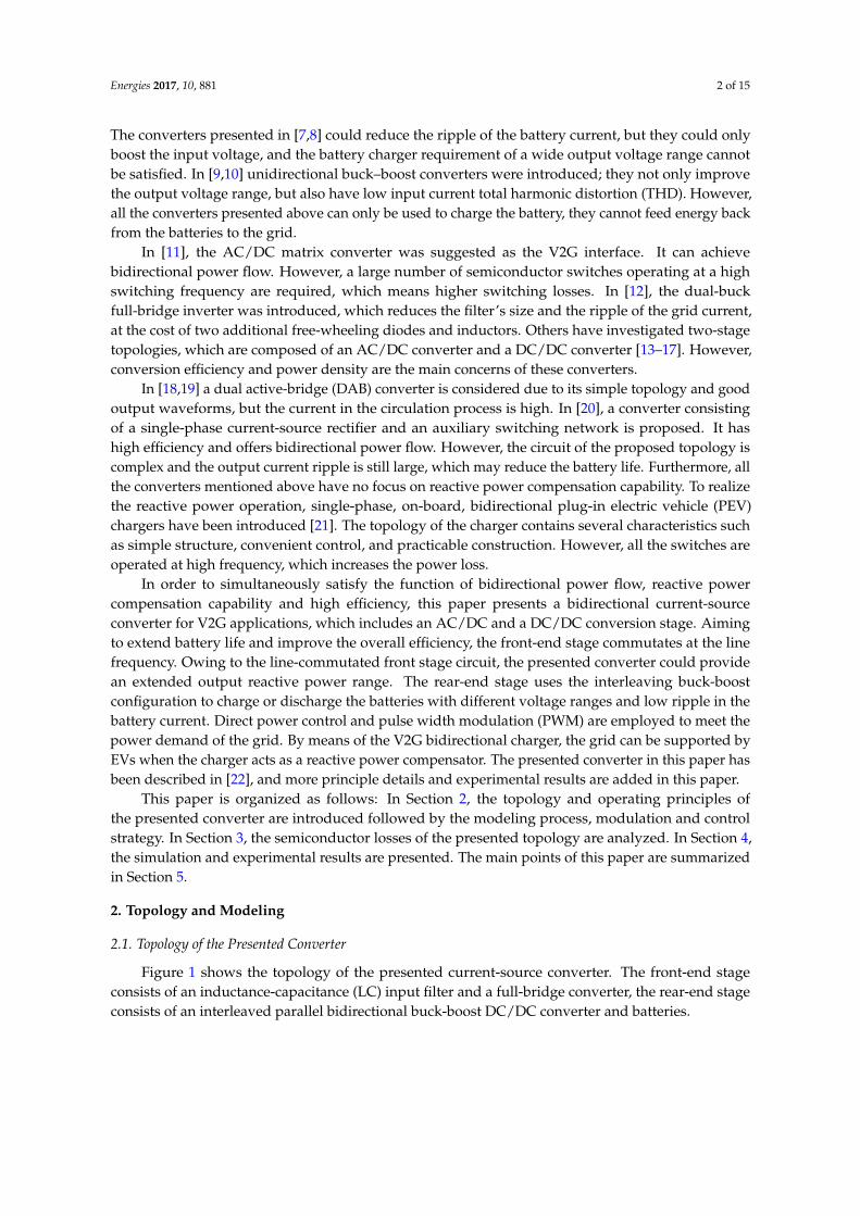
Figure 1 shows the topology of the presented current-source converter. The front-end stageconsists of an inductance-capacitance (LC) input filter and a full-bridge converter, the rear-end stageconsists of an interleaved parallel bidirectional buck-boost DC/DC converter and batteries.
Energies 2017, 10, 881 3 of 15Energies 2017, 10, 881 3 of 16
uC
ig
idc
iL1 iL2
Lg
ug C
S1 S3 S5D1 D3 D5
S2 S4
S6D2 D4
D6L1 L2
S7D7
S8D8 ib
iL Co
Bat
tery
ub
The front-end stage
The rear-end stage
Figure 1. The presented bidirectional converter topology.
The LC input filter is used to prevent the high-frequency harmonic currents generated by the converter from flowing into grid. The full-bridge converter is used to rectify the AC input voltage to a DC voltage or invert the DC voltage to an AC voltage. Moreover, the bidirectional power flow is achieved. To improve the converter efficiency, the switches of the full-bridge converter commutate at the line frequency. The interleaved parallel bidirectional buck-boost DC/DC converter is employed to reduce the battery current ripple. Additionally, power factor correction (PFC) and high input current quality can be realized with the topology.
2.2. Operation Mode
Taking the charging state as an example, the operation of the presented converter topology is shown in Figure 2. Assume the duty-cycle d1 is less than 0.5 and the grid voltage gu is greater than
zero, the operation mode is shown as follows.
ig
idc
iL1 iL2
Lg
ug C uC
S1 S3 S5D1 D3 D5
S2 S4
S6
D2 D4
D6L1 L2
S7D7
S8D8 ib
iL Co
Bat
tery
ub
ig
iL1 iL2
Lg
ug C uC
S1 S3 S5D1 D3 D5
S2 S4
S6
D2 D4
D6L1 L2
S7D7
S8D8 ib
iL Co
Bat
tery
ub
ig
idc
iL1 iL2
Lg
ug C uC
S1 S3 S5D1 D3 D5
S2 S4
S6
D2 D4
D6L1 L2
S7D7
S8D8 ib
iL Co
Bat
tery
ub
ig
iL1 iL2
Lg
ug C uC
S1 S3 S5D1 D3 D5
S2 S4
S6
D2 D4
D6L1 L2
S7D7
S8D8 ib
iL Co
Bat
tery
ub
(a)(b)
(c)(d) Figure 2. The operation mode of the interleaved parallel bidirectional buck-boost DC/DC circuit.
State 1 (t1–t2): from Figure 2a, S5, S8 are on, S6, S7 are off. The voltage across inductor L1 is expressed as:
1Lu = | gu |.
1Lu is positive, increasing linearly with a slope of (| gu |)/L. And the
energy is transferred from the grid to the inductor L1. The voltage across inductor L2 is expressed as:
Figure 1. The presented bidirectional converter topology.
The LC input filter is used to prevent the high-frequency harmonic currents generated by theconverter from flowing into grid. The full-bridge converter is used to rectify the AC input voltage toa DC voltage or invert the DC voltage to an AC voltage. Moreover, the bidirectional power flow isachieved. To improve the converter efficiency, the switches of the full-bridge converter commutate atthe line frequency. The interleaved parallel bidirectional buck-boost DC/DC converter is employed toreduce the battery current ripple. Additionally, power factor correction (PFC) and high input currentquality can be realized with the topology.
2.2. Operation Mode
Taking the charging state as an example, the operation of the presented converter topology isshown in Figure 2. Assume the duty-cycle d1 is less than 0.5 and the grid voltage ug is greater thanzero, the operation mode is shown as follows.
Energies 2017, 10, 881 3 of 16
uC
ig
idc
iL1 iL2
Lg
ug C
S1 S3 S5D1 D3 D5
S2 S4
S6D2 D4
D6L1 L2
S7D7
S8D8 ib
iL Co
Bat
tery
ub
The front-end stage
The rear-end stage
Figure 1. The presented bidirectional converter topology.
The LC input filter is used to prevent the high-frequency harmonic currents generated by the converter from flowing into grid. The full-bridge converter is used to rectify the AC input voltage to a DC voltage or invert the DC voltage to an AC voltage. Moreover, the bidirectional power flow is achieved. To improve the converter efficiency, the switches of the full-bridge converter commutate at the line frequency. The interleaved parallel bidirectional buck-boost DC/DC converter is employed to reduce the battery current ripple. Additionally, power factor correction (PFC) and high input current quality can be realized with the topology.
2.2. Operation Mode
Taking the charging state as an example, the operation of the presented converter topology is shown in Figure 2. Assume the duty-cycle d1 is less than 0.5 and the grid voltage gu is greater than
zero, the operation mode is shown as follows.
ig
idc
iL1 iL2
Lg
ug C uC
S1 S3 S5D1 D3 D5
S2 S4
S6
D2 D4
D6L1 L2
S7D7
S8D8 ib
iL Co
Bat
tery
ub
ig
iL1 iL2
Lg
ug C uC
S1 S3 S5D1 D3 D5
S2 S4
S6
D2 D4
D6L1 L2
S7D7
S8D8 ib
iL Co
Bat
tery
ub
ig
idc
iL1 iL2
Lg
ug C uC
S1 S3 S5D1 D3 D5
S2 S4
S6
D2 D4
D6L1 L2
S7D7
S8D8 ib
iL Co
Bat
tery
ub
ig
iL1 iL2
Lg
ug C uC
S1 S3 S5D1 D3 D5
S2 S4
S6
D2 D4
D6L1 L2
S7D7
S8D8 ib
iL Co
Bat
tery
ub
(a)(b)
(c)(d) Figure 2. The operation mode of the interleaved parallel bidirectional buck-boost DC/DC circuit.
State 1 (t1–t2): from Figure 2a, S5, S8 are on, S6, S7 are off. The voltage across inductor L1 is expressed as:
1Lu = | gu |.
1Lu is positive, increasing linearly with a slope of (| gu |)/L. And the
energy is transferred from the grid to the inductor L1. The voltage across inductor L2 is expressed as:
Figure 2. The operation mode of the interleaved parallel bidirectional buck-boost DC/DC circuit.
State 1 (t1–t2): from Figure 2a, S5, S8 are on, S6, S7 are off. The voltage across inductor L1 isexpressed as: uL1 = |ug|. uL1 is positive, increasing linearly with a slope of (|ug|)/L. And the energy istransferred from the grid to the inductor L1. The voltage across inductor L2 is expressed as: uL2 = −ub,
Energies 2017, 10, 881 4 of 15
uL2 is negative, iL2 decreases linearly with a slope of (ub)/L. The energy stored in the inductor L2 istransferred to the battery.
State 2 (t2–t3): from Figure 2b, S6, S8 are on and S5, S7 are off. The energy in the inductors L1, L2 istransferred to the battery through S6 and S8. During this interval, the two inductor currents iL1 and iL2
decrease linearly with a slope of (ub)/L.State 3 (t3–t4): from Figure 2c, S6, S7 are on and S5, S8 are off. uL2 is positive and the energy is
transferred from the grid to the inductor L2. uL1 is negative and the energy stored in the inductor L1 istransferred to the battery.
State 4 (t4–t5): from Figure 2d, S6, S8 are on and S5, S7 are off. This state is the same as state 2,so the energy in the inductors L1, L2 is transferred to the battery through S6 and S8.
In addition, the converter is able to work in other modes, and the similar analysis method can beapplied. Therefore, due to space limits, the details are neglected here.
2.3. Modeling of the Presented Topology
According to Figure 1, assume that the system works in continuous conduction mode, the statespace average model for the presented charger topology is formulated as follows:
ug = Um sin(ωt)ig = Im sin(ωt + ϕ)
Lg digdt = ug − uc
C ducdt = ig− sgn(uC)d1iL
idc = sgn(ug)ig
iL = iL1 + iL2
L diLdt = d1|uC| − (1− d1)ub
(1)
where ug is the grid voltage; ig is the input current; Um and Im are the amplitude of the grid voltage andthe input current, respectively. ϕ is the power factor angle. If ϕ ∈ (−π/2, π/2), the grid will chargethe batteries of the EV; if ϕ ∈ (−π,−π/2) ∪ (π/2, π), the batteries of the EV will be discharged.More importantly, active power and reactive power are absorbed from the grid or supported to thegrid depending on power factor angle ϕ that is listed in Table 1. Lg and C are the inductance andcapacitance of the input filter, respectively; uC is the terminal voltage of capacitor C; idc is the currenton DC side; ub is the battery voltage; iL1 and iL2 are the two inductor currents; d1 is the duty-cycle ofswitches S5 and S7; (1 − d1) is the duty-cycle of switches S6 and S8; sgn( ) is the sign function.
Table 1. The active and reactive power related to phase angle.
Phase Angle Active Power (P) Reactive Power (Q)
ϕ ∈ (−π,−π/2) P < 0, dischargingQ > 0 Reactive power absorbingϕ = −π/2 P = 0
ϕ ∈ (−π/2, 0) P > 0, charging
ϕ = 0 P > 0, charging Q = 0
ϕ ∈ (0, π/2) P > 0, chargingQ < 0 Reactive power supportingϕ = π/2 P = 0
ϕ ∈ (π/2, π) P < 0, discharging
ϕ = π P < 0, discharging Q = 0
If the input filter is designed properly, the effect of the input filter can be neglected, then ug ≈ uc.Based on voltage-second balance principle:
d1|uC| = (1− d1)ub (2)
Energies 2017, 10, 881 5 of 15
idc = d1iL (3)
According to Equation (2), d1 can be obtained as follows:
d1 =ub
|uC|+ ub(4)
The sum of two inductor current iL can be given by:
iL =sgn(uc)ig
d1=
sgn(uc)ig(|uC|+ ub)
ub(5)
In practical application, the current iL can be controlled to guarantee ig approach sine wave. It iseasy to find that the input displacement angle of the presented converter ranges from −π/2 to π/2.
2.4. Modulation and Control Strategy
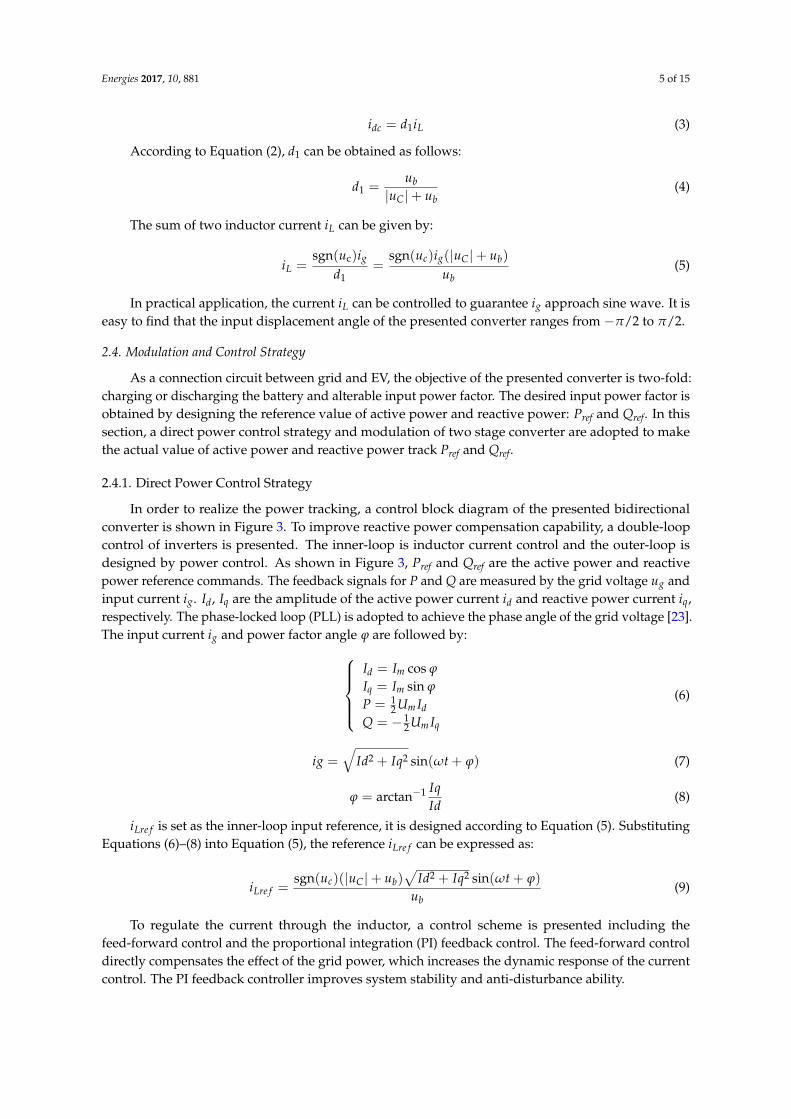
As a connection circuit between grid and EV, the objective of the presented converter is two-fold:charging or discharging the battery and alterable input power factor. The desired input power factor isobtained by designing the reference value of active power and reactive power: Pref and Qref. In thissection, a direct power control strategy and modulation of two stage converter are adopted to makethe actual value of active power and reactive power track Pref and Qref.
2.4.1. Direct Power Control Strategy
In order to realize the power tracking, a control block diagram of the presented bidirectionalconverter is shown in Figure 3. To improve reactive power compensation capability, a double-loopcontrol of inverters is presented. The inner-loop is inductor current control and the outer-loop isdesigned by power control. As shown in Figure 3, Pref and Qref are the active power and reactivepower reference commands. The feedback signals for P and Q are measured by the grid voltage ug andinput current ig. Id, Iq are the amplitude of the active power current id and reactive power current iq,respectively. The phase-locked loop (PLL) is adopted to achieve the phase angle of the grid voltage [23].The input current ig and power factor angle ϕ are followed by:
Id = Im cos ϕ
Iq = Im sin ϕ
P = 12 Um Id
Q = − 12 Um Iq
(6)
ig =√
Id2 + Iq2 sin(ωt + ϕ) (7)
ϕ = arctan−1 IqId
(8)
iLre f is set as the inner-loop input reference, it is designed according to Equation (5). SubstitutingEquations (6)–(8) into Equation (5), the reference iLre f can be expressed as:
iLre f =sgn(uc)(|uC|+ ub)
√Id2 + Iq2 sin(ωt + ϕ)
ub(9)
To regulate the current through the inductor, a control scheme is presented including thefeed-forward control and the proportional integration (PI) feedback control. The feed-forward controldirectly compensates the effect of the grid power, which increases the dynamic response of the currentcontrol. The PI feedback controller improves system stability and anti-disturbance ability.
Energies 2017, 10, 881 6 of 15
Energies 2017, 10, 881 6 of 16
Lrefi is set as the inner-loop input reference, it is designed according to Equation (5).
Substituting Equations (6)–(8) into Equation (5), the reference Lrefi can be expressed as:
( )( ) 2 2sgn sin( t )ω ϕ+ ++=
dc Cf
qbLre
b
u u ui
I
u
I (9)
Reference inductor current calculation
(9)P,Q calculation
(6)c
cs
ωω+
LPFPI
PI
PI
PWM
P
Q
Qref
Pref
iLref
iL
ug
ig
Id
Iq
( )+b
c b
u
u u
PLLug tω
Figure 3. Control block diagram of the presented converter.
To regulate the current through the inductor, a control scheme is presented including the feed-forward control and the proportional integration (PI) feedback control. The feed-forward control directly compensates the effect of the grid power, which increases the dynamic response of the current control. The PI feedback controller improves system stability and anti-disturbance ability.
2.4.2. Modulation of the Two-Stage Converter
In the presented converter, the front-end stage AC/DC converter operates at the line frequency and the PWM modulation is adopted in the rear-end converter.
The front-end stage AC/DC converter operates at the line frequency, as shown in Figure 4. The power factor of the grid is alternative. Sg1 is the switch level signal of S1, S4; Sg2 is the switch level signal of S2, S3. When the grid voltage gu is greater than zero, the switches S1 and S4 are turned on;
switches S2, S3 are turned off. When gu is less than zero, S1 and S4 are turned off, while S2, S3 are
turned on.
1
0
1
0
Sg1
Sg2
Voltage ug Current ig
t/s
t/s
t/s
Figure 4. The front-end stage AC/DC converter operates at the line frequency.
The rear-end interleaved DC/DC converter adopts PWM modulation. From Figure 1, it has two identical inductors: L1 = L2 = L. Due to its configuration and modulation, it has low battery current
Figure 3. Control block diagram of the presented converter.
2.4.2. Modulation of the Two-Stage Converter
In the presented converter, the front-end stage AC/DC converter operates at the line frequencyand the PWM modulation is adopted in the rear-end converter.
The front-end stage AC/DC converter operates at the line frequency, as shown in Figure 4. Thepower factor of the grid is alternative. Sg1 is the switch level signal of S1, S4; Sg2 is the switch levelsignal of S2, S3. When the grid voltage ug is greater than zero, the switches S1 and S4 are turned on;switches S2, S3 are turned off. When ug is less than zero, S1 and S4 are turned off, while S2, S3 areturned on.
Energies 2017, 10, 881 6 of 16
Lrefi is set as the inner-loop input reference, it is designed according to Equation (5).
Substituting Equations (6)–(8) into Equation (5), the reference Lrefi can be expressed as:
( )( ) 2 2sgn sin( t )ω ϕ+ ++=
dc Cf
qbLre
b
u u ui
I
u
I (9)
Reference inductor current calculation
(9)P,Q calculation
(6)c
cs
ωω+
LPFPI
PI
PI
PWM
P
Q
Qref
Pref
iLref
iL
ug
ig
Id
Iq
( )+b
c b
u
u u
PLLug tω
Figure 3. Control block diagram of the presented converter.
To regulate the current through the inductor, a control scheme is presented including the feed-forward control and the proportional integration (PI) feedback control. The feed-forward control directly compensates the effect of the grid power, which increases the dynamic response of the current control. The PI feedback controller improves system stability and anti-disturbance ability.
2.4.2. Modulation of the Two-Stage Converter
In the presented converter, the front-end stage AC/DC converter operates at the line frequency and the PWM modulation is adopted in the rear-end converter.
The front-end stage AC/DC converter operates at the line frequency, as shown in Figure 4. The power factor of the grid is alternative. Sg1 is the switch level signal of S1, S4; Sg2 is the switch level signal of S2, S3. When the grid voltage gu is greater than zero, the switches S1 and S4 are turned on;
switches S2, S3 are turned off. When gu is less than zero, S1 and S4 are turned off, while S2, S3 are
turned on.
1
0
1
0
Sg1
Sg2
Voltage ug Current ig
t/s
t/s
t/s
Figure 4. The front-end stage AC/DC converter operates at the line frequency.
The rear-end interleaved DC/DC converter adopts PWM modulation. From Figure 1, it has two identical inductors: L1 = L2 = L. Due to its configuration and modulation, it has low battery current
Figure 4. The front-end stage AC/DC converter operates at the line frequency.
The rear-end interleaved DC/DC converter adopts PWM modulation. From Figure 1, it has twoidentical inductors: L1 = L2 = L. Due to its configuration and modulation, it has low battery currentripple. As shown in Figure 5a,b, the shifted angle between the pulses of power switches S3 and S5 is π.Similarly, the pulses of power switches S4 and S6, mutually shifted, are the same. This modulation canreduce the battery current ripple to extend its life. To provide a bidirectional energy flow, the switchesS5, S6 are in a complementary conduction state, as are the switches S7 and S8. The pulses of switchesS5, S6, S7, S8, and the two inductor currents iL1 , iL2 are shown in Figure 5a. The total inductor currentiL (iL = iL1 + iL2 ) has little ripple.
Energies 2017, 10, 881 7 of 15
Energies 2017, 10, 881 7 of 16
ripple. As shown in Figure 5a,b, the shifted angle between the pulses of power switches S3 and S5 is π. Similarly, the pulses of power switches S4 and S6, mutually shifted, are the same. This modulation can reduce the battery current ripple to extend its life. To provide a bidirectional energy flow, the switches S5, S6 are in a complementary conduction state, as are the switches S7 and S8.The pulses of switches S5, S6, S7, S8, and the two inductor currents
1Li ,
2Li are shown in Figure 5a. The
total inductor current Li ( Li = 1Li +
2Li ) has little ripple.
≥ d1
≥ d1
180ºphase delay
s5
s6
s7
s8
not
not
(a) (b)
S5
S7
iL1
iL2
iL
t1 t2 t3 t4 t5
S6
S8
Figure 5. (a) The switch pulses and two inductor currents of the interleaved DC/DC converter; (b) The PWM modulation of the interleaved DC/DC converter.
3. Power Loss Analysis
To comprehend converter performance, calculation and analysis of the converter power loss are crucial, which influence the thermal design and predict the system efficiency. The power losses can be divided into two parts: semiconductor losses and passive components losses. In the presented converter, the semiconductor losses play the main role. Based on this, the power loss calculation of the semiconductors has become a top priority. In general, the semiconductor losses consist of conduction loss and switching loss, which shows a correlation with switching frequencies, current densities, and power requirements. In [24,25], the two main kinds of power semiconductor losses calculation formulas are as following.
Conduction loss:
( ) ( )( )200
1 T
CS CE c CE cP u i t r i t dtT
= +
(10)
( ) ( )( )200
1 T
CD D D D DP u i t r i t dtT
= ⋅ + ⋅ (11)
where T is the period of the integrated function, PCS and PCD are the conduction loss of the insulated gate bipolar transistor (IGBT) and the conduction loss of the anti-parallel diode, respectively. 0CEu and 0Du are the forward voltages when the current is zero, they can be acquired by the
incremental resistances of the IGBT CEr , the diode Dr , and the flowing current ci or Di . Switching loss:
0
Ts
SWT SWTR R
f v iP E dt
T V I= (12)
0
TsSWD SWD
R R
f v iP E dt
T V I= (13)
Figure 5. (a) The switch pulses and two inductor currents of the interleaved DC/DC converter; (b) ThePWM modulation of the interleaved DC/DC converter.
3. Power Loss Analysis
To comprehend converter performance, calculation and analysis of the converter power loss arecrucial, which influence the thermal design and predict the system efficiency. The power losses canbe divided into two parts: semiconductor losses and passive components losses. In the presentedconverter, the semiconductor losses play the main role. Based on this, the power loss calculation of thesemiconductors has become a top priority. In general, the semiconductor losses consist of conductionloss and switching loss, which shows a correlation with switching frequencies, current densities,and power requirements. In [24,25], the two main kinds of power semiconductor losses calculationformulas are as following.
Conduction loss:
PCS =1T
∫ T
0
(uCE0ic(t) + rCEi2c (t)
)dt (10)
PCD =1T
∫ T
0
(uD0 · iD(t) + rD · i2D(t)
)dt (11)
where T is the period of the integrated function, PCS and PCD are the conduction loss of the insulatedgate bipolar transistor (IGBT) and the conduction loss of the anti-parallel diode, respectively. uCE0and uD0 are the forward voltages when the current is zero, they can be acquired by the incrementalresistances of the IGBT rCE, the diode rD, and the flowing current ic or iD.
Switching loss:
PSWT =fs
T
∫ T
0ESWT
vVR
iIR
dt (12)
PSWD =fs
T
∫ T
0ESWD
vVR
iIR
dt (13)
where fs is the switching frequency, PSWT and PSWD are the switching loss of the IGBT and the diodereverse recovery loss, respectively. ESWT is the switching loss energy in the reference conditions(VR and IR), it includes the turn-on energy Eon_T and the turn-off energy Eoff_T of the IGBT. ESWDmainly includes the reverse recovery losses Err_D. Thus, it should be converted into the actual workingconditions (v and i).
Based on the control and modulation scheme mentioned above, it’s obvious that the presentedconverter has the same switching losses in charge or discharge mode and the conduction losses aredifferent in these modes. Taking the charge mode, for example, in the front-end stage, the switchesoperate at line frequency, the conduction loss has become main part of the semiconductor loss andthe switching loss has been neglected. The semiconductor loss in the rear-end interleaved parallelbuck-boost converter consists of conduction loss and switching loss. Taking one arm S5, S6 for instance,in terms of switching loss, in the state 1 (S5 is on and S6 is off), the current iL charge the inductor through
Energies 2017, 10, 881 8 of 15
S5. In the next state (state 2: S5 is off and S6 is on) the current iL flows through the free-wheeling diodeD6. Then, in the last state (S5 is on and S6 is off), this state is similar to the state 1: S5 turns on and S6
is off, the current iL charge the inductor through S5 and the diode D6 turn off. During this cyclicalprocess, the turn-on and turn-off losses of S5 and reverse recovery loss of D6 are produced. Similarly,the conduction loss of the rear-end stage is mainly produced by the IGBT because of the neglected lowconduction loss of body diode. In other modes, the analysis process for the other switches is similar.
From the front-end stage, the converter has two switches in the conducting state at any time.So the loss of the front-end stage can be expressed as:
PC_ f ront = 2PCD =2T
∫ T
0
(uD0 · iD(t) + rD · i2D(t)
)dt (14)
From the rear-end stage, the converter has two parallel branches in DC/DC part. Assume that theroot mean square (rms) of the total DC current is Idc, each branch current is Idc/2. The collector-emittervoltage rms of the switch is USW . The conduction loss PC_rear and the switching loss PSW_rear of therear-end stage can be calculated by:
PC_rear = 2
[(VD0 + VCE0)
Idc2
+ (rD + rCE)
(Idc2
)2]
(15)
PSW_rear = 2fsUSW
Idc2
VR IR
(Eon_T + Eo f f _T + Err_D
)iL1 (16)
The core losses Pcore of DC inductor L1 and L2 can be calculated as:
Pcore = 2KcoreVcore( fs)m(Bac)
n (17)
where Kcore is the coefficient of the core material. Vcore is the effective core volume. Bac is the peak fluxdensity. m and n is the frequency exponent and flux density exponent, respectively.
The wire losses Pdcr of DC inductor L1 and L2 caused by DC resistance can be calculated as:
Pdcr = 2I2rmsRdc (18)
where Irms is the rms value of the peak current applied to the inductor, Rdc is the DC resistance ofthe inductor.
The total losses PL of DC inductor L1 and L2 can be calculated as:
PL = Pcore + Pdcr (19)
Finally, in the unity charging mode, the total loss of this AC/DC converter Ptotal can be acquiredby equations:
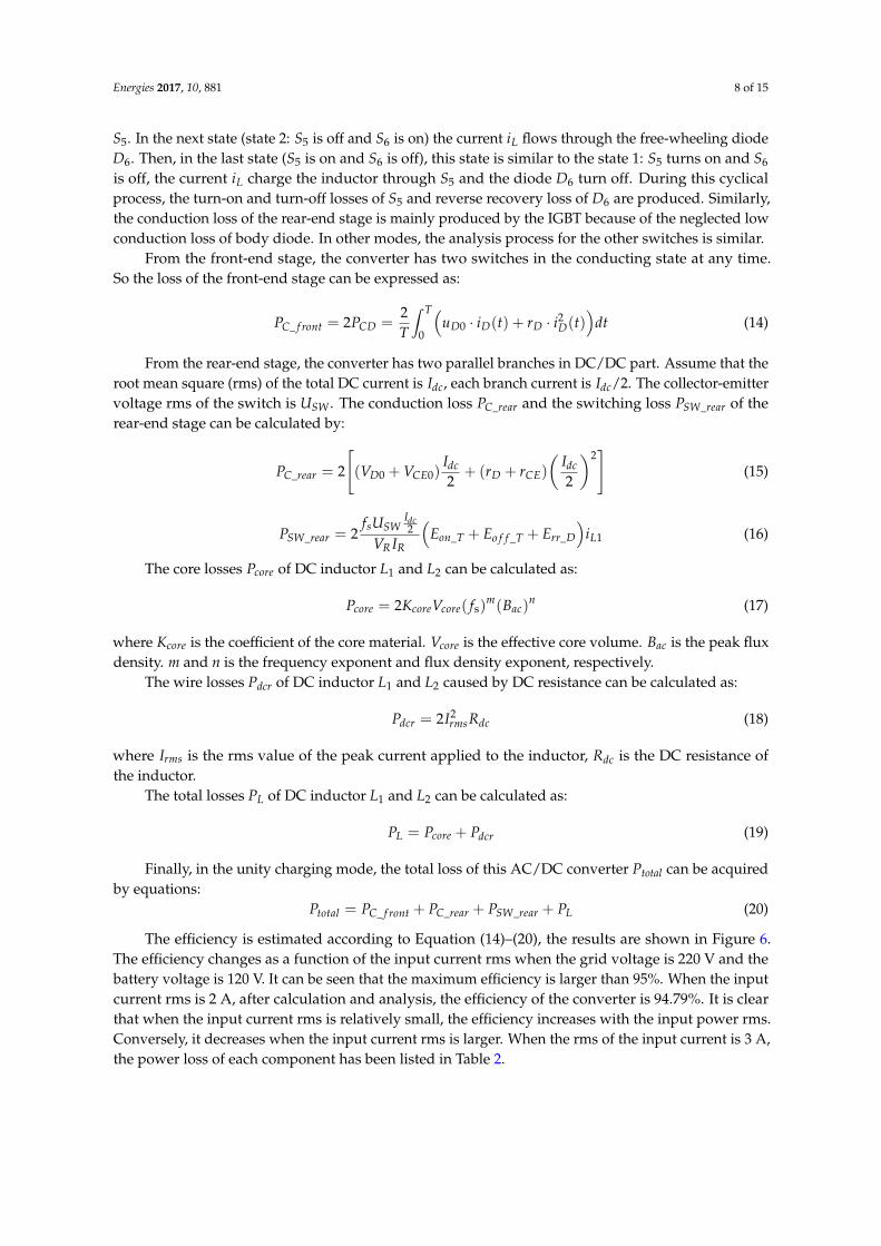
The efficiency is estimated according to Equation (14)–(20), the results are shown in Figure 6.The efficiency changes as a function of the input current rms when the grid voltage is 220 V and thebattery voltage is 120 V. It can be seen that the maximum efficiency is larger than 95%. When the inputcurrent rms is 2 A, after calculation and analysis, the efficiency of the converter is 94.79%. It is clearthat when the input current rms is relatively small, the efficiency increases with the input power rms.Conversely, it decreases when the input current rms is larger. When the rms of the input current is 3 A,the power loss of each component has been listed in Table 2.
Energies 2017, 10, 881 9 of 15
Energies 2017, 10, 881 9 of 16
Finally, in the unity charging mode, the total loss of this AC/DC converter Ptotal can be acquired by equations:
_ _total C front C rear SW_rear LP P P P P= + + + (20)
The efficiency is estimated according to Equation (14)–(20), the results are shown in Figure 6. The efficiency changes as a function of the input current rms when the grid voltage is 220 V and the battery voltage is 120 V. It can be seen that the maximum efficiency is larger than 95%. When the input current rms is 2 A, after calculation and analysis, the efficiency of the converter is 94.79%. It is clear that when the input current rms is relatively small, the efficiency increases with the input power rms. Conversely, it decreases when the input current rms is larger. When the rms of the input current is 3 A, the power loss of each component has been listed in Table 2.
Figure 6. Efficiency variation with the input current rms.
Table.2. The power loss of each component when the rms of input current is 3 A.
Power Loss Values
Front-end stage conduction loss of diodes Pc_d_front 8.94 W Rear-end stage switching loss of IGBT Psw_T_rear 6.73 W
Rear-end stage reverse-recovery loss of diodes Psw_d_rear 7.30 W Rear-end stage conduction loss of diodes Pc_d_rear 3.68 W Rear-end stage conduction loss of IGBT Pc_T_rear 3.89 W
The losses of DC inductors PL 3.06 W
4. Simulation and Experimental Results
4.1. Simulation Results
To validate the V2G bidirectional converter topology, simulations are implemented based on the MATLAB/Simulink environment in this section. The models of the semiconductor device and battery are from the SimPowerSystem/Power Electronics library. The schematic diagram of the presented bidirectional converter in the simulation is shown in Figure 1. The parameters used in the simulation are listed in Table 3. A switching frequency of 20 kHz is selected with the trade-off between THD and the converter efficiency. An input filter is used to avoid overvoltage and reduce input current distortion. The DC inductors L1 and L2 are working in the linear area of flux density-magnetic field strength (B-H) curve. The loads are 38 Ah-capacity lead-acid batteries with a nominal voltage of 120 V.
Figure 6. Efficiency variation with the input current rms.
Table 2. The power loss of each component when the rms of input current is 3 A.
Power Loss Values
Front-end stage conduction loss of diodes Pc_d_front 8.94 WRear-end stage switching loss of IGBT Psw_T_rear 6.73 W
Rear-end stage reverse-recovery loss of diodes Psw_d_rear 7.30 WRear-end stage conduction loss of diodes Pc_d_rear 3.68 WRear-end stage conduction loss of IGBT Pc_T_rear 3.89 W
The losses of DC inductors PL 3.06 W
4. Simulation and Experimental Results
4.1. Simulation Results
To validate the V2G bidirectional converter topology, simulations are implemented based on theMATLAB/Simulink environment in this section. The models of the semiconductor device and batteryare from the SimPowerSystem/Power Electronics library. The schematic diagram of the presentedbidirectional converter in the simulation is shown in Figure 1. The parameters used in the simulationare listed in Table 3. A switching frequency of 20 kHz is selected with the trade-off between THDand the converter efficiency. An input filter is used to avoid overvoltage and reduce input currentdistortion. The DC inductors L1 and L2 are working in the linear area of flux density-magnetic fieldstrength (B-H) curve. The loads are 38 Ah-capacity lead-acid batteries with a nominal voltage of 120 V.
Table 3. Simulation parameters.
Parameters Values
The amplitude of voltage Ug 311 VInput filter inductance (Lg) 0.8 mH
Output filter capacitor (Co) 103 uFSwitching frequency (fs) 20 kHz
Battery voltage (ub) 120 V
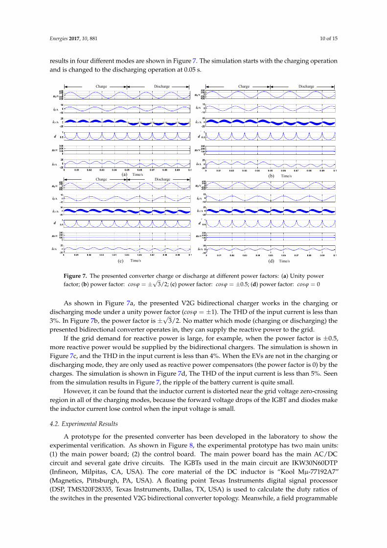
The simulation results shown in Figure 7 show the performance of the presented converter. Fromthe top to bottom, the grid voltage ug, the input current ig; the inductor L1 current iL1 ; the duty-cycle ofswitch S5; the battery voltage ub and the battery current ib are sequentially displayed. The simulation
Energies 2017, 10, 881 10 of 15
results in four different modes are shown in Figure 7. The simulation starts with the charging operationand is changed to the discharging operation at 0.05 s.
Energies 2017, 10, 881 10 of 16
Table 3. Simulation parameters.
Parameters Values
The amplitude of voltage Ug 311 V Input filter inductance (Lg) 0.8 mH
The simulation results shown in Figure 7 show the performance of the presented converter. From the top to bottom, the grid voltage gu , the input current gi ; the inductor L1 current
1Li ; the
duty-cycle of switch S5; the battery voltage bu and the battery current bi are sequentially displayed. The simulation results in four different modes are shown in Figure 7. The simulation starts with the charging operation and is changed to the discharging operation at 0.05 s.
(a) (b)
(c) (d)
ug/V
ig/A
iL1/A
ub/V
ib/A
d
Charge DischargeCharge Discharge
Charge Discharge
ug/V
ig/A
iL1/A
d
ub/V
ib/A
ug/V
ig/A
iL1/A
d
ub/V
ib/A
ug/V
ig/A
iL1/A
d
ub/V
ib/A
Time/s Time/s
Time/s Time/s
Figure 7. The presented converter charge or discharge at different power factors: (a) Unity power factor; (b) power factor: = ±√3/2; (c) power factor: = ±0.5; (d) power factor: = 0.
As shown in Figure 7a, the presented V2G bidirectional charger works in the charging or discharging mode under a unity power factor ( = ±1). The THD of the input current is less than 3%. In Figure 7b, the power factor is ±√3/2. No matter which mode (charging or discharging) the presented bidirectional converter operates in, they can supply the reactive power to the grid.
If the grid demand for reactive power is large, for example, when the power factor is ±0.5, more reactive power would be supplied by the bidirectional chargers. The simulation is shown in Figure 7c, and the THD in the input current is less than 4%. When the EVs are not in the charging or discharging mode, they are only used as reactive power compensators (the power factor is 0) by the
Figure 7. The presented converter charge or discharge at different power factors: (a) Unity powerfactor; (b) power factor: cosϕ = ±
√3/2; (c) power factor: cosϕ = ±0.5; (d) power factor: cosϕ = 0
As shown in Figure 7a, the presented V2G bidirectional charger works in the charging ordischarging mode under a unity power factor (cosϕ = ±1). The THD of the input current is less than3%. In Figure 7b, the power factor is ±
√3/2. No matter which mode (charging or discharging) the
presented bidirectional converter operates in, they can supply the reactive power to the grid.If the grid demand for reactive power is large, for example, when the power factor is ±0.5,
more reactive power would be supplied by the bidirectional chargers. The simulation is shown inFigure 7c, and the THD in the input current is less than 4%. When the EVs are not in the charging ordischarging mode, they are only used as reactive power compensators (the power factor is 0) by thecharges. The simulation is shown in Figure 7d, The THD of the input current is less than 5%. Seenfrom the simulation results in Figure 7, the ripple of the battery current is quite small.
However, it can be found that the inductor current is distorted near the grid voltage zero-crossingregion in all of the charging modes, because the forward voltage drops of the IGBT and diodes makethe inductor current lose control when the input voltage is small.
4.2. Experimental Results
A prototype for the presented converter has been developed in the laboratory to show theexperimental verification. As shown in Figure 8, the experimental prototype has two main units:(1) the main power board; (2) the control board. The main power board has the main AC/DCcircuit and several gate drive circuits. The IGBTs used in the main circuit are IKW30N60DTP(Infineon, Milpitas, CA, USA). The core material of the DC inductor is “Kool Mµ-77192A7”(Magnetics, Pittsburgh, PA, USA). A floating point Texas Instruments digital signal processor(DSP, TMS320F28335, Texas Instruments, Dallas, TX, USA) is used to calculate the duty ratios ofthe switches in the presented V2G bidirectional converter topology. Meanwhile, a field programmable
Energies 2017, 10, 881 11 of 15
gate array (FPGA, EP2C8T144C8N, Altera Corporation, San Jose, CA, USA) is used for implementingthe operation mode of the switches.
Energies 2017, 10, 881 11 of 16
charges. The simulation is shown in Figure 7d, The THD of the input current is less than 5%. Seen from the simulation results in Figure 7, the ripple of the battery current is quite small.
However, it can be found that the inductor current is distorted near the grid voltage zero-crossing region in all of the charging modes, because the forward voltage drops of the IGBT and diodes make the inductor current lose control when the input voltage is small.
4.2. Experimental Results
A prototype for the presented converter has been developed in the laboratory to show the experimental verification. As shown in Figure 8, the experimental prototype has two main units: (1) the main power board; (2) the control board. The main power board has the main AC/DC circuit and several gate drive circuits. The IGBTs used in the main circuit are IKW30N60DTP (Infineon, Milpitas, CA, USA). The core material of the DC inductor is “Kool Mμ-77192A7” (Magnetics, Pittsburgh, PA, USA). A floating point Texas Instruments digital signal processor (DSP, TMS320F28335, Texas Instruments, Dallas, TX, USA) is used to calculate the duty ratios of the switches in the presented V2G bidirectional converter topology. Meanwhile, a field programmable gate array (FPGA, EP2C8T144C8N, Altera Corporation, San Jose, CA, USA) is used for implementing the operation mode of the switches.
Control board
Main power board
Semiconductor switches
Figure 8. A prototype for the presented converter.
The experimental results presented in Figures 9–11 show the operation of the presented single-phase bidirectional converter with the battery voltage 120 V/38 Ah and the grid voltage in the charging mode. In Figure 12, the presented converter operates under unity power factor in the discharging mode. The experimental results of the grid voltage, input current, inductor current, and battery voltage under different conditions are presented in Figures 9–12. The THD values of the input current in Figures 9–12 have been presented in Table 4, respectively.
Figure 8. A prototype for the presented converter.
The experimental results presented in Figures 9–11 show the operation of the presentedsingle-phase bidirectional converter with the battery voltage 120 V/38 Ah and the grid voltagein the charging mode. In Figure 12, the presented converter operates under unity power factor inthe discharging mode. The experimental results of the grid voltage, input current, inductor current,and battery voltage under different conditions are presented in Figures 9–12. The THD values of theinput current in Figures 9–12 have been presented in Table 4, respectively.Energies 2017, 10, 881 12 of 16
(300V/div)
(5A/div)
(5A/div)
(100V/div)bu
gugi
(10ms/div)
1Li
Figure 9. The experimental waveform of the presented converter operating in charging mode under a unity power factor (P = 400 W, Q = 0 var, = 1).
(300V/div)
(5A/div)
(5A/div)
(100V/div)bu
gugi
(10ms/div)
1Li
Figure 10. The experimental waveform of the presented converter operating in the charging mode (P = 200 W, Q = −340 var, = 0.5).
(300V/div)
(5A/div)
(5A/div)
(100V/div)
gigu
bu
(10ms/div)
1Li
Figure 11. The experimental waveform of the presented converter operating as reactive power compensation equipment (P = 0, Q = −400 var, = 0).
Figure 9. The experimental waveform of the presented converter operating in charging mode under aunity power factor (P = 400 W, Q = 0 var, cosϕ = 1.
Energies 2017, 10, 881 12 of 15
Energies 2017, 10, 881 12 of 16
(300V/div)
(5A/div)
(5A/div)
(100V/div)bu
gugi
(10ms/div)
1Li
Figure 9. The experimental waveform of the presented converter operating in charging mode under a unity power factor (P = 400 W, Q = 0 var, = 1).
(300V/div)
(5A/div)
(5A/div)
(100V/div)bu
gugi
(10ms/div)
1Li
Figure 10. The experimental waveform of the presented converter operating in the charging mode (P = 200 W, Q = −340 var, = 0.5).
(300V/div)
(5A/div)
(5A/div)
(100V/div)
gigu
bu
(10ms/div)
1Li
Figure 11. The experimental waveform of the presented converter operating as reactive power compensation equipment (P = 0, Q = −400 var, = 0).
Figure 10. The experimental waveform of the presented converter operating in the charging mode(P = 200 W, Q = −340 var, cosϕ = 0.5.
Energies 2017, 10, 881 12 of 16
(300V/div)
(5A/div)
(5A/div)
(100V/div)bu
gugi
(10ms/div)
1Li
Figure 9. The experimental waveform of the presented converter operating in charging mode under a unity power factor (P = 400 W, Q = 0 var, = 1).
(300V/div)
(5A/div)
(5A/div)
(100V/div)bu
gugi
(10ms/div)
1Li
Figure 10. The experimental waveform of the presented converter operating in the charging mode (P = 200 W, Q = −340 var, = 0.5).
(300V/div)
(5A/div)
(5A/div)
(100V/div)
gigu
bu
(10ms/div)
1Li
Figure 11. The experimental waveform of the presented converter operating as reactive power compensation equipment (P = 0, Q = −400 var, = 0).
Figure 11. The experimental waveform of the presented converter operating as reactive powercompensation equipment (P = 0, Q = −400 var, cosϕ = 0.Energies 2017, 10, 881 13 of 16
(300V/div)
(5A/div)
(5A/div)
(100V/div)bu
gu gi
(10ms/div)
1Li
Figure 12. The experimental waveform of the presented converter operating in the discharging mode under a unity power factor (P = −400 W, Q = 0 var, = −1).
Table.4. The THD values of input current under different conditions.
Condition The THD of Input Current
P = 400 W, Q = 0 var, = 1 6.15%
P = 200 W, Q = −340 var, = 0.5 18.33%
P = 0, Q = −400 var, = 0 34.58%
P = −400 W, Q = 0 var, = −1 7.31%
In the charging mode, the presented converter operated under a unity power factor, as shown in Figure 9. The active power P is 400 W, and the THD value of the input current is nearly sinusoidal. In other conditions, as shown in Figure 10, the power factor is 0.5, the active power P is 200 W, and the reactive power Q is −340 var. The THD value of the input current is worse than the condition under a unity power factor. Obviously, the converter has supported a part of reactive power. Especially, the presented converter can be operated as reactive power equipment compensation as presented in Figure 11. It does not transmit active power in this condition. The power factor angle is π/2 and the reactive power is −400 var. However, it can be found that the inductor current is distorted near the grid voltage zero-crossing region in non-unity power factor modes, which leads to distortion of the input current. This is because the forward voltage drops of the IGBT and diode make the inductor current lose control when the input voltage is small. To feed energy back to the grid, the converter should operate in the discharging mode. As shown in Figure 12, the converter operates under a unity power factor in the discharging mode, and the active power is −400 W. It can be seen that the power factor angle between input current and grid voltage is almost π. In addition, the input current is nearly sinusoidal. Due to the converter’s interleaved configuration and modulation, it can be seen that the total inductor current ripple has been reduced in Figures 13 and 14. All the experimental results mentioned above show that the presented converter is suitable to take an indispensable role for V2G applications.
Figure 12. The experimental waveform of the presented converter operating in the discharging modeunder a unity power factor (P = −400 W, Q = 0 var, cosϕ = −1.
Table 4. The THD values of input current under different conditions.
Condition The THD of Input Current
P = 400 W, Q = 0 var, cosϕ = 1 6.15%P = 200 W, Q = −340 var, cosϕ = 0.5 18.33%
P = 0, Q = −400 var, cosϕ = 0 34.58%P = −400 W, Q = 0 var, cosϕ = −1 7.31%
Energies 2017, 10, 881 13 of 15
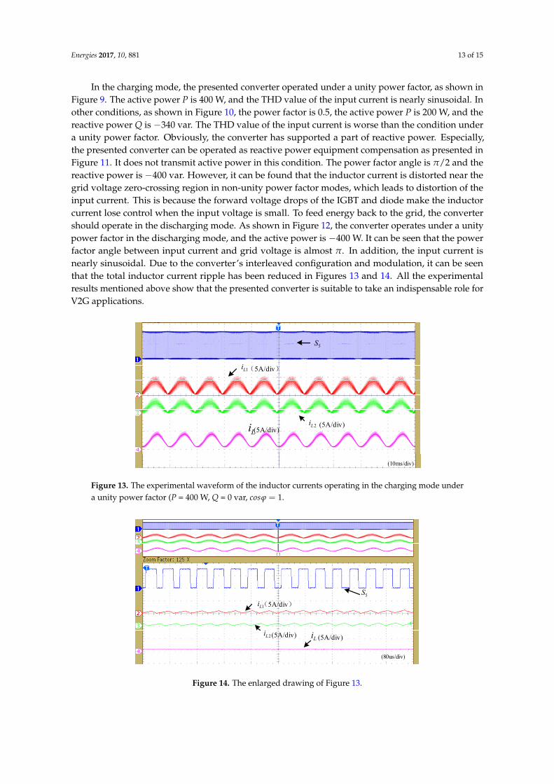
In the charging mode, the presented converter operated under a unity power factor, as shown inFigure 9. The active power P is 400 W, and the THD value of the input current is nearly sinusoidal. Inother conditions, as shown in Figure 10, the power factor is 0.5, the active power P is 200 W, and thereactive power Q is −340 var. The THD value of the input current is worse than the condition undera unity power factor. Obviously, the converter has supported a part of reactive power. Especially,the presented converter can be operated as reactive power equipment compensation as presented inFigure 11. It does not transmit active power in this condition. The power factor angle is π/2 and thereactive power is −400 var. However, it can be found that the inductor current is distorted near thegrid voltage zero-crossing region in non-unity power factor modes, which leads to distortion of theinput current. This is because the forward voltage drops of the IGBT and diode make the inductorcurrent lose control when the input voltage is small. To feed energy back to the grid, the convertershould operate in the discharging mode. As shown in Figure 12, the converter operates under a unitypower factor in the discharging mode, and the active power is −400 W. It can be seen that the powerfactor angle between input current and grid voltage is almost π. In addition, the input current isnearly sinusoidal. Due to the converter’s interleaved configuration and modulation, it can be seenthat the total inductor current ripple has been reduced in Figures 13 and 14. All the experimentalresults mentioned above show that the presented converter is suitable to take an indispensable role forV2G applications.Energies 2017, 10, 881 14 of 16
(5A/div)
(5A/div)(5A/div)
Li
(10ms/div)
5S
1Li
2Li
Figure 13. The experimental waveform of the inductor currents operating in the charging mode under a unity power factor (P = 400 W, Q = 0 var, = 1).
(5A/div)1Li
(5A/div)2Li Li
5S
(5A/div)
(80us/div)
Figure 14. The enlarged drawing of Figure 13.
5. Conclusions
In this paper a single-phase bidirectional AC/DC converter for V2G applications has been presented. This topology consists of a line frequency-commutated unfolding bridge and an interleaved buck-boost stage. The circuit operates in buck-boost charging/discharging condition, and offers different voltage levels for all types of batteries. The operation principle of the presented charger topology has been analyzed and it has been shown that reactive power can be supported and exchanged with the grid using the presented bidirectional charger. Moreover, the presented charger has a number of attractive features, such as bidirectional power flow, low current ripple, and a wide battery voltage range. Thus, it is a good candidate for V2G applications. The simulation and experimental results have been presented to verify the effectiveness of the V2G bidirectional charger.
Acknowledgments: This work was supported by the Major Program of the National Natural Science Foundation of China under grants 61490702 and 61573384, and the Fundamental Research Funds for the Central Universities of Central South University under Grant 2017zzts687.
Author Contributions: Peng Yang conceived the main idea and wrote the manuscript with guidance from Tao Peng and Hui Wang. Hao Wang and Hui Dong performed the experiments; Hanbing Dan, Hua Han, Jian Yang and Patrick wheeler reviewed the work and gave helpful improvement suggestions.
Conflicts of Interest: The authors declare no conflict of interest.
References
Figure 13. The experimental waveform of the inductor currents operating in the charging mode undera unity power factor (P = 400 W, Q = 0 var, cosϕ = 1.
Energies 2017, 10, 881 14 of 16
(5A/div)
(5A/div)(5A/div)
Li
(10ms/div)
5S
1Li
2Li
Figure 13. The experimental waveform of the inductor currents operating in the charging mode under a unity power factor (P = 400 W, Q = 0 var, = 1).
(5A/div)1Li
(5A/div)2Li Li
5S
(5A/div)
(80us/div)
Figure 14. The enlarged drawing of Figure 13.
5. Conclusions
In this paper a single-phase bidirectional AC/DC converter for V2G applications has been presented. This topology consists of a line frequency-commutated unfolding bridge and an interleaved buck-boost stage. The circuit operates in buck-boost charging/discharging condition, and offers different voltage levels for all types of batteries. The operation principle of the presented charger topology has been analyzed and it has been shown that reactive power can be supported and exchanged with the grid using the presented bidirectional charger. Moreover, the presented charger has a number of attractive features, such as bidirectional power flow, low current ripple, and a wide battery voltage range. Thus, it is a good candidate for V2G applications. The simulation and experimental results have been presented to verify the effectiveness of the V2G bidirectional charger.
Acknowledgments: This work was supported by the Major Program of the National Natural Science Foundation of China under grants 61490702 and 61573384, and the Fundamental Research Funds for the Central Universities of Central South University under Grant 2017zzts687.
Author Contributions: Peng Yang conceived the main idea and wrote the manuscript with guidance from Tao Peng and Hui Wang. Hao Wang and Hui Dong performed the experiments; Hanbing Dan, Hua Han, Jian Yang and Patrick wheeler reviewed the work and gave helpful improvement suggestions.
Conflicts of Interest: The authors declare no conflict of interest.
References
Figure 14. The enlarged drawing of Figure 13.
Energies 2017, 10, 881 14 of 15
5. Conclusions
In this paper a single-phase bidirectional AC/DC converter for V2G applications has beenpresented. This topology consists of a line frequency-commutated unfolding bridge and an interleavedbuck-boost stage. The circuit operates in buck-boost charging/discharging condition, and offersdifferent voltage levels for all types of batteries. The operation principle of the presented chargertopology has been analyzed and it has been shown that reactive power can be supported and exchangedwith the grid using the presented bidirectional charger. Moreover, the presented charger has a numberof attractive features, such as bidirectional power flow, low current ripple, and a wide battery voltagerange. Thus, it is a good candidate for V2G applications. The simulation and experimental resultshave been presented to verify the effectiveness of the V2G bidirectional charger.
Acknowledgments: This work was supported by the Major Program of the National Natural Science Foundationof China under grants 61490702 and 61573384, and the Fundamental Research Funds for the Central Universitiesof Central South University under Grant 2017zzts687.
Author Contributions: Peng Yang conceived the main idea and wrote the manuscript with guidance fromTao Peng and Hui Wang. Hao Wang and Hui Dong performed the experiments; Hanbing Dan, Hua Han, Jian Yangand Patrick wheeler reviewed the work and gave helpful improvement suggestions.
Conflicts of Interest: The authors declare no conflict of interest.
References
1. Kempton, W.; Tomic, J. Vehicle-to-grid power fundamentals: Calculating capacity and net revenue.J. Power Sources 2005, 144, 268–279. [CrossRef]
2. Viswanathan, V.V.; Kintner-Meyer, M. Second use of transportation batteries: Maximizing the value ofbatteries for transportation and grid services. IEEE Trans. Veh. Technol. 2011, 60, 2963–2970. [CrossRef]
3. Sortomme, E.; El-Sharkawi, M.A. Optimal scheduling of vehicle-to-grid energy and ancillary services.IEEE Trans. Smart Grid 2012, 3, 351–359. [CrossRef]
4. Yilmaz, M.; Krein, P.T. Review of the impact of vehicle-to-grid technologies on distribution systems andutility interfaces. IEEE Trans. Power Electron. 2013, 28, 5673–5689. [CrossRef]
6. Jang, M.; Ciobotaru, M.; Agelidis, V.G. A compact single-phase bidirectional buck-boost inverter topology.In Proceedings of the 2012 International Conference on Renewable Energy Research and Applications(ICRERA), Nagasaki, Japan, 11–14 November 2012; pp. 1–6.
7. Jang, Y.; Jovanovic, M.M. Interleaved boost converter with intrinsic voltage-doubler characteristic foruniversal-line PFC front end. IEEE Trans. Power Electron. 2007, 22, 1394–1401. [CrossRef]
9. Lopez, O.; De Vicuna, L.C.; Castilla, M.; Matas, J.; Lopez, M. Sliding-mode-control design of ahigh-power-factor buck-boost rectifier. IEEE Trans. Ind. Electron. 1999, 46, 604–612. [CrossRef]
10. Ghanem, M.C.; Al-Haddad, K.; Roy, G. A new control strategy to achieve sinusoidal line current in a cascadebuck-boost converter. IEEE Trans. Ind. Electron. 1996, 43, 441–449. [CrossRef]
11. Su, M.; Wang, H.; Sun, Y.; Yang, J.; Xiong, W.; Liu, Y. AC/DC matrix converter with an optimized modulationstrategy for V2G applications. IEEE Trans. Power Electron. 2013, 28, 5736–5745. [CrossRef]
12. Li, B.; Huang, S.; Chen, X. Performance improvement for two-stage single-phase grid-connected convertersusing a fast dc bus control scheme and a novel synchronous frame current controller. Energies 2017, 10, 389.[CrossRef]
13. Ngo, T.; Lee, K.; Won, J.; Nam, K. Study of single-phase bidirectional battery charger for high powerapplication. In Proceedings of the 7th International Power Electronics and Motion Control Conference(IPEMC), Harbin, China, 2–5 June 2012; pp. 958–962.
14. Wong, N.; Kazerani, M. A review of bidirectional on-board charger topologies for plugin vehicles.In Proceedings of the 25th IEEE Canadian Conference on Electrical & Computer Engineering (CCECE),Montreal, QC, Canada, 29 April–2 May 2012; pp. 1–6.
15. Shin, J.; Lee, J.Y. An electrolytic capacitor-less bi-directional EV on-board charger using harmonic modulationtechnique. IEEE Trans. Power Electron. 2014, 29, 5195–5203. [CrossRef]
16. Yilmaz, M.; Krein, P.T. Review of battery charger topologies, charging power levels, and infrastructure forplug-in electric and hybrid vehicles. IEEE Trans. Power Electron. 2013, 28, 2151–2169. [CrossRef]
17. Choi, J.; Byen, B.; Lee, Y.; Han, D.; Kho, H.; Choe, G. Design of leakage inductance in resonant dc-dc converterfor electric vehicle charger. IEEE Trans. Magn. 2012, 48, 4417–4420. [CrossRef]
18. Rosekeit, M.; Broeck, C.; De Doncker, R.W. Dynamic control of a dual active bridge for bidirectional accharging. In Proceedings of the IEEE International Conference on Industrial Technology (ICIT), Seville,Spain, 17–19 March 2015; pp. 2085–2091.
19. Xue, L.; Shen, Z.; Boroyevich, D.; Mattavelli, P.; Diaz, D. Dual active bridge-based battery charger for plug-inhybrid electric vehicle with charging current containing low frequency ripple. IEEE Trans. Power Electron.2015, 30, 7299–7307. [CrossRef]
20. Han, H.; Liu, Y.; Sun, Y.; Wang, H.; Su, M. A single-phase current-source bidirectional converter for V2Gapplications. J. Power Electron. 2014, 14, 458–467. [CrossRef]
22. Yang, P.; Peng, T.; Wang, H.; Han, H.; Yang, J.; Wang, H. A single-phase current-source bidirectional converterfor V2G application. In Proceedings of the IEEE 3rd International Future Energy Electronics Conference 2017and ECCE Asia (IFEEC 2017-ECCEAsia), Kaohsiung, Taiwan, 3–7 June 2017.
23. Luo, Z.; Su, M.; Sun, Y.; Liu, Z.; Dong, M. First-order generalized integrator based frequency-locked loop andsynchronization for three-phase grid-connected converters under adverse grid conditions. J. Power Electron.2016, 16, 1939–1949. [CrossRef]
24. Bierhoff, M.H.; Fuchs, F.W. Semiconductor losses in voltage source and current source IGBT converters basedon analytical derivation. In Proceedings of the IEEE 35th Annual Power Electronics Specialists Conference,Aachen, Germany, 20–25 June 2004; pp. 2836–2842.
25. Wang, B.; Venkataramanan, G. Analytical modeling of semiconductor losses in matrix converters.In Proceedings of the 5th International Power Electronics and Motion Control Conference, Shanghai, China,14–16 August 2006; pp. 1–8.