Page 1
A Sliding-Mode Controller with Zero Forced
Zero PWM for Full Bridge Inverter
Shunshi Zhong, Xiucheng Dong, and Xiaomei Yu XiHua University, City, CountryChina
Email: {zhongshunshi, dxc136, yuxiaomei}@163.com
Abstract—Sliding mode control scheme for the full bridge
inverter was analyzed, including modeling the variable
structure system, selecting the switching line and control
law. To make maximum use of degrees of freedom of the full
bridge inverter circuit switching device, the idea of the
single polarity sine pulse width modulation (SPWM) is
introduced to the sliding mode control in full bridge inverter
to reduce the switching loss. Furthermore, zero forced zero
sliding mode PWM is used to suppress voltage distortion
caused by sliding mode surface passing zero modulation.
Simulation results are given to verify the correctness and
validity of implemented zero forced zero sliding mode PWM
for full bridge inverter.
Index Terms—sliding mode control, full bridge inverter,
variable structure system, pulse width modulation.
I. INTRODUCTION
In recent years, sliding mode control method gradually
attracted the attention of scholars [1]. Its biggest
advantage is that sliding mode has fully adaptive to
interference and perturbation on the system, and once the
system state enters into the sliding mode motion, it
quickly converges to the control objective [2]-[4]. As the power conversion device for DC/AC, Inverter
has become an indispensable electrical device for production and living. Such as UPS, AC motor drives and car adapter, etc [1], [3]. The design of this kind of inverters requires high efficiency, highly stable output voltage and low harmonic distortion [5]-[7]. At the same time it should be considered that the inverter output has rapid dynamic property and stable robustness in the case of unstable input voltage and frequent load change [8]-[10]. Normally the inverter adopts SPWM to guarantee the low distortion of the output voltage waveform, and stabilizes the output voltage amplitude by the output voltage RMS feedback and routine control [11]-[13]. But this control method needs longer time to recover when facing the load change and its dynamic property is rather poor. Especially when there are intermediate requirements for the dynamic property of the inverter, it is difficult for the traditional control method to satisfy [1]-[4], [10]. Based on the variable structure system theory, sliding-mode control shows the insensitivity, robustness and good dynamic property for system parameters change and load change, which can be applied
Manuscript received March 1, 2015; revised June 1, 2015.
to control the inherent variable structure system of the inverter. Document [10] firstly applies sliding-mode control to single-phase inverter, and then gives the switching line and control action, and experimental results verify the advantage of sliding-mode control. Document [14] analyzes sliding-mode control inverter systematically. These can show that sliding-mode control inverter has good dynamic property and robustness. Furthermore, many sliding-mode methods are analyzed for inverter [1]-[4], [15]-[16].
This paper conducts a research on the key design
technology of sliding-mode control full bridge inverter,
and sets up the variable structure model, determining
switching line and switch control law. To make
maximum use of degrees of freedom of the full bridge
inverter circuit switching device, the idea of the single
polarity sine pulse width modulation (SPWM) is
introduced to the sliding mode control in full bridge
inverter to reduce the switching loss. Furthermore, zero
forced zero sliding mode PWM is used to suppress
voltage distortion caused by sliding mode surface passing
zero modulation. Simulation results are given to verify
the correctness and validity of implemented zero forced
zero sliding mode PWM for full bridge inverter.
II. THE MATHEMATICAL MODEL OF FULL BRIDGE
INVERTER
Power conversion circuit structure of the full bridge
inverter is shown in Fig. 1. Inverter can generate three
different phase voltage uinv(+E, 0 and -E) through four
switch (Q1, Q2, Q3, Q4) with different sets of switch
connected the dc power supply to the ac output side.
When Q1 and Q3 are turned on, it gives uinv=+E. When
Q2 and Q4 are turned on, it gives uinv=-E. When Q1, Q2
or Q3, Q4 are turned on, it gives uinv=0. The relationship
between output level and switch state is shown in Table I.
Switch state ‘1’ means the switch is on and ‘0’ means the
switch is off.
E
Q1
Q4
Q2
Q3
L
C Ruinv
Figure 1. The Structure of full bridge inverter.
Journal of Automation and Control Engineering Vol. 4, No. 3, June 2016
©2016 Journal of Automation and Control Engineering 204doi: 10.18178/joace.4.3.204-208
Page 2
TABLE I. THE RELATIONSHIP BETWEEN OUTPUT LEVEL AND
SWITCH STATE.
uinv Q1 Q3 Q4 Q2 Output
condition
E 1 1 0 0 P
0 0 1 1 0
O 1 0 0 1
-E 0 0 1 1 N
Ac square wave voltage output is converted to
sinusoidal output voltage by the LC low pass filter.
Output filter capacitor voltage and its derivative are
continuous measurable, so capacitor voltage and its
derivative are regarded as phase variables of the system
to describe the system. System state equation is shown in
Eq. (1).
uLCEu
u
RCLCu
u
c
c
c
c
/
0
/1/1
10
(1)
where 1,1u , while u=1, uinv=E; while u=-1, uinv=-E.
Eq. (1) can be used as a variable structure model of the
full bridge inverter. The derivative of output capacitor
voltage can be got by capacitor voltage and capacitance
current as shown in Eq. (2).
Ciu / (2)
Thus, as long as the reference output signal is known,
the difference between the reference signals and state
variables can be regarded as a new state variables. So
system state equation is shown in Eq. (3).
LCVRCVVu
LCE
uV
uV
RCLCuV
uV
refrefref
cref
cref
cref
cref
//
0
/
0
/1/1
10
(3)
III. THE SLIDING MODE CONTROL OF FULL BRIDGE
INVERTER
On the phase plane as shown in Eq. (3), a straight line,
which get through the origin with negative slope is
selected as switch line, namely:
0])([])([),( 21 crefcrefc utVkutVktu (4)
The structure diagram of sliding mode control is
shown in Fig. 2. In order to make the system state
trajectory along the slide switch line and eventually stable
at the origin, k1 and k2 are ensured to be positive,
i.e. 01 k , 02 k . On the switch line, dynamic sliding
mode area is a first order dynamic process as shown in Eq.
(4). Solution to the output voltage Uc(t) for dynamic
process is:
21 /)()(
ktk
refc etVtu
(5)
The dynamic process of the output voltage of inverter
working in sliding mode surface is determined by the
ratio (k1/k2) of the switching surface coefficient and the
initial state (μ) when the state trajectory reach the
switching surface, and has nothing to do with the other
parameters of the system, which embodies the robustness
of sliding state system to external disturbance and change
of internal parameters. Due to the variable structure
system described by Eq. (1) includes two subsystems,
each has a unique equilibrium point. As long as the
switching line make balance point respectively in its two
sides and system equilibrium point is located in the
opposite side of switch line, the switch line is accessible.
As a result, control function is as follows:
0,1
0,1
u (6)
ccrefrefeq u
LCu
RCVV
E
LCtu
11)( (7)
where 0/ 21 kk .
Sinusoidal
reference
signal
k1
k2
Hysteresis
comparator
Full bridge
inverter
Filter
and load
Vref
Uc
Vref.
Uc.
+
+
++
-
-
Figure 2. Block diagram of sliding mode control.
IV. SINGLE POLARITY SLIDING MODE PWM
For full bridge inverter circuit, inverter output voltage
using single polarity SPWM has only zero level and a
positive or negative level in each switch cycle, which
makes two switching devices in the conduction on or off
state for a long time, reducing the switch losses and
output voltage jump. To make maximum use of degrees
of freedom of the full bridge inverter circuit switching
device, the idea of the single polarity SPWM will be
introduced to the sliding mode control in full bridge
inverter. In Fig. 1, in the process of the whole modulation,
a switch tube can be kept conducting, and another switch
tube in the high frequency switch state. When P state is
needed for output in Table I, Q1 has been in the
conducting state and Q3 can be modulated by the sliding
mode controller; When P status is needed for output in
Table I, Q2 has been in the conducting state and Q4 can
be modulated by the sliding mode controller. As shown in
Fig. 3, drive pulse waveforms (ug1, ug3) of switch tube
(Q1, Q3) is compared. Thereinto, ug1 is power frequency
square wave, and ug3 is got by the switch function as Eq.
(8).
0,0
0,13
gu (8)
Journal of Automation and Control Engineering Vol. 4, No. 3, June 2016
©2016 Journal of Automation and Control Engineering 205
While 0 , the corresponding equivalent control is
as follows:
Page 3
Ug3
Ug1
21
2
1
0
0
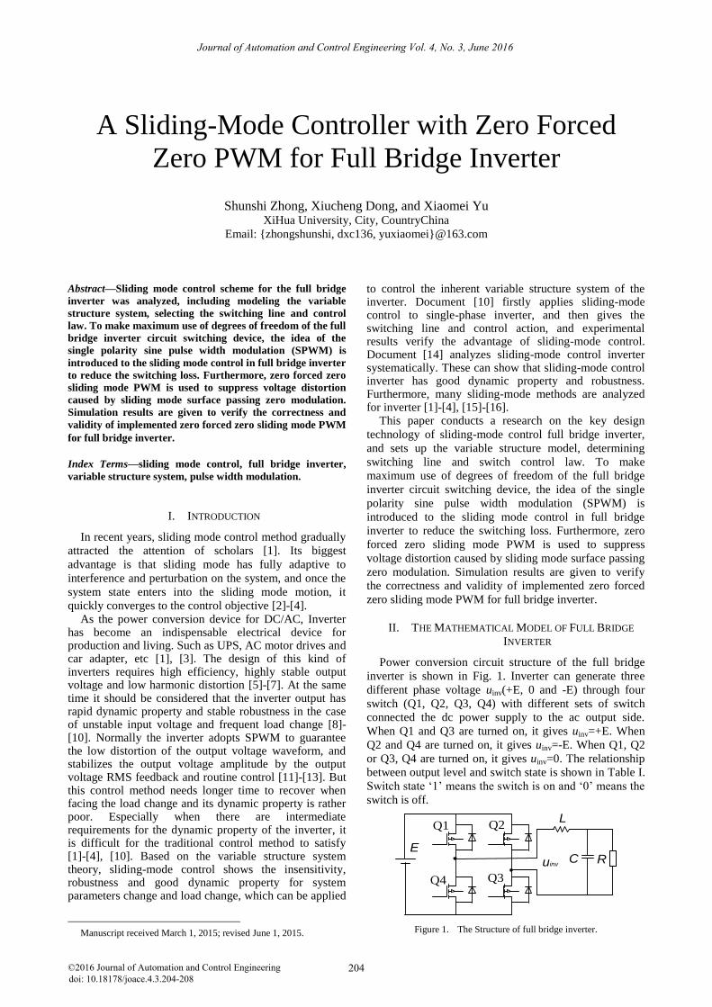
Figure 3. Drive pulse waveform (ug1, ug3) of switch tube (Q1, Q3).
A problem exists in the process of single polarity
sliding-mode PWM control as shown in Fig. 4. When the
sinusoidal output voltage each passes zero, the two low
frequency switches of full bridge inverter need switch
over, namely, ug1 and ug4 drive pulse signal switching
between 0 and 1. If the other two high frequency switches
have not yet returned to the sliding surface at this time,
modulation will have a big deviation. For example, when
the sinusoidal output voltage is passing zero potential
from positive to negative, i.e. ug1 changed from 1 to 0,
ug4 changed from 0 to 1. If the ug2, ug3 did not return to
the sliding mode surface, i.e. they keep on pulse
condition of the moment before. At the same time, if the
ug2 is 1, ug3 is 0. In this way, ug2 and ug4 is conducting
state, as a result the output is -E, which can be got from
Table I. According to the principle of PWM modulation,
when sinusoidal output pass the zero point, modulation
pulse needed should be 0, otherwise the output voltage
distortion happens.
t(s)=0.01s
2
2
1
0
1
1
0
2
0
Ug3
Ug1
Figure 4. Single polarity sliding-mode PWM directly.
In order to solve the above problems, zero forced zero
sliding-mode PWM is used to suppress voltage distortion
caused by this kind of sliding mode surface passing zero
modulation. Every time when sinusoidal output voltage
pass zero, the other two drive pulse of high frequency
switch devices (ug2, ug3) are forced to 0. Thus,
44
11
gx22
gx33
u'u
u'u
u*u'u
u*u'u
gg
gg
gg
gg
(9)
where ugx is square wave signal, the duty cycle is
determined by sampling period (Ts).
There is a further discussion about time of zero forced
zero. If time of zero forced zero is too short, it may result
in the incomplete elimination for sliding mode surface
passing zero modulation, thus the surplus and even the
opposite modulating pulse will result in the distortion of
the output voltage; If time of zero forced zero is too long,
it may influence the successive half cycle of normal
sliding mode PWM. After analyzing, it is found that the
influence time of sliding mode surface passing zero
modulation will be a switch cycle at most, so time of zero
forced zero can be determined.
V. SIMULATION RESULTS
In order to verify the correctness and validity of
implemented zero forced zero sliding mode PWM for full
bridge inverter in this paper, the simulation is
investigated under the environment of Matlab/Simulink.
The specific circuit and the control parameters are as
follows:
The input voltage: E=60V;
Filter parameters and the rated load: L=500μH,
C=20μF, R=40ῼ;
The sliding coefficient: k1=12,k2=0.005;
Hysteresis width and switching frequency:
2h=20,fs=5kHz.
Fig. 5 is pulse waveform of single polarity sliding-
mode PWM directly. In 0.01s and 0.02s, which is half a
power frequency cycle, ug2 and ug3 will take sliding
mode surface passing zero modulation. Fig. 6 is pulse
waveform of zero forced zero single polarity sliding-
mode PWM. Obviously, sliding-mode surface zero
modulation pulse is removed in ug2 and ug3, becoming
zero immediately after 0.01s or 0.02s.
Figure 5. Pulse waveform of single polarity sliding-mode PWM
directly.
Figure 6. Pulse waveform of zero forced zero single polarity sliding-mode PWM.
Journal of Automation and Control Engineering Vol. 4, No. 3, June 2016
©2016 Journal of Automation and Control Engineering 206
Page 4
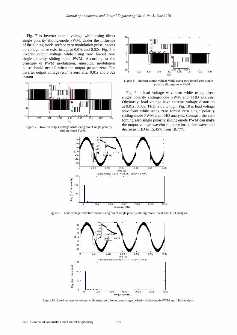
Fig. 7 is inverter output voltage while using direct
single polarity sliding-mode PWM. Under the influence
of the sliding mode surface zero modulation pulse, excess
dc voltage pulse exist in uinv at 0.01s and 0.02s. Fig. 8 is
inverter output voltage while using zero forced zero
single polarity sliding-mode PWM. According to the
principle of PWM modulation, sinusoidal modulation
pulse should need 0 when the output passed zero. The
inverter output voltage (uinv) is zero after 0.01s and 0.02s
instant.
Figure 7. Inverter output voltage while using direct single polarity sliding-mode PWM.
Figure 8. Inverter output voltage while using zero forced zero single polarity sliding-mode PWM.
Fig. 9 is load voltage waveform while using direct
single polarity sliding-mode PWM and THD analysis.
Obviously, load voltage have extreme voltage distortion
at 0.01s, 0.02s, THD is quite high. Fig. 10 is load voltage
waveform while using zero forced zero single polarity
sliding-mode PWM and THD analysis. Contrast, the zero
forcing zero single polarity sliding-mode PWM can make
the output voltage waveform approximate sine wave, and
decrease THD to 15.45% from 18.77%.
Figure 9. Load voltage waveform while using direct single polarity sliding-mode PWM and THD analysis.
Figure 10. Load voltage waveform while using zero forced zero single polarity sliding-mode PWM and THD analysis.
Journal of Automation and Control Engineering Vol. 4, No. 3, June 2016
©2016 Journal of Automation and Control Engineering 207
Page 5
VI. CONCLUSION
A sliding mode control scheme for the full bridge
inverter was analyzed, including modeling the variable
structure system, selecting the switching line and control
law. To make maximum use of degrees of freedom of the
full bridge inverter circuit switching device, the idea of
the single polarity sine pulse width modulation is
introduced to the sliding mode control in full bridge
inverter to reduce the switching loss. Furthermore, zero
forced zero sliding mode PWM is used to suppress
voltage distortion caused by sliding mode surface passing
zero modulation. Simulation results have verified the
correctness and validity of implemented zero forced zero
sliding mode PWM for full bridge inverter.
ACKNOWLEDGMENT
This work is partially supported by Fund of Power
Electronic Energy Saving Technology and Equipment
Key laboratory (No.szjj2014-013); Fund of Postgraduate,
Xihua university (NO: ycjj2014074); Fund of Major
Education Project of Sichuan Provincial Education
Department (NO: 13ZC0003); the Technical Supporting
Programs of Sichuan Province (NO: 2013GZX0152). The
authors also gratefully acknowledge the helpful
comments and suggestions of the reviewers, which have
improved the presentation.
REFERENCES
[1] J. Hu, L. Shang, Y. He, and Z. Q. Zhu, “Direct active and reactive
power regulation of grid-connected DC/AC converters using sliding mode control approach,” IEEE Trans. Power Electron., vol.
26, no. 1, pp. 210-222, Jan. 2011.
[2] F. Fuchs, J. Dannehl, and F. W. Fuchs, “Discrete sliding mode current control of grid-connected three-phase PWM converters
with LCL filter,” in Proc. IEEE Int. Symp. Ind. Electron., 2010, pp. 779-785.
[3] T. Tai and J. Chen, “UPS inverter design using discrete-time
sliding-mode control scheme,” IEEE Trans. Ind. Electron, vol. 49, no. 1, pp. 67–75, Feb. 2002.
[4] J. Matas, L. G. de Vicuna, J. Miret, J. M. Guerrero, and M. Castilla, “Feedback linearization of a single-phase active power
filter via sliding mode control,” IEEE Trans. Power Electron., vol.
23, no. 1, pp. 116–125, Jan. 2008.
[5] C. Cecati, C. Citro, and P. Siano, “Combined operations of
renewable energy systems and responsive demand in a smart grid,” IEEE Trans. Sustainable Energy, vol. 2, no. 2, pp. 468–476,
Oct. 2011.
[6] D. Dong, I. Cvetkovic, D. Boroyevich, W. Zhang, R. Wang, and P. Mattavelli, “Grid-interface bidirectional converter for residential
dc distribution systems-part one: High-density two-stage topology,” IEEE Trans. Power Electron., vol. 28, no. 4, pp. 1655–
1666, Apr. 2013.
[7] M. Brenna, G. Lazaroiu, and E. Tironi, “High power quality and DG integrated low voltage dc distribution system,” presented at
the IEEE Power Eng. Soc. Gen. Meet., Montreal, QC, Canada, 2006.
[8] A. Cid-Pastor, L. Mart ı́nez-Salamero, A. El Aroudi, R. Giral, J.
Calvente, and R. Leyva, “Synthesis of loss-free resistors based on sliding-mode control and its applications in power processing,”
Contr. Eng. Practice, vol. 21, pp. 689–699, May 2013. [9] A. Cid-Pastor, L. Mart´ınez-Salamero, C. Alonso, B. Estibals, J.
Alzieu, G. Schweitz, and D. Shmilovitz, “Analysis and design of
power gyrators in sliding-mode operation,” IEE Proc. Electr. Power Appl., vol. 152, no. 4, pp. 821–826, July 2005.
[10] K. Jezernik and D. Zadravec, “Sliding mode controller for a
single phase inverter [C],” in Proc. APEC’90, Los Angeles, 1990,
1(S), pp. 185-190.
[11] Y. Liang and C. O. Nwankpa, “A new type of STATCOM based on cascading voltage-source inverters with phase-shifted unipolar
SPWM,” IEEE Transactions on Industry Applications, vol. 35, no. 5, pp. 1118–1123, 1999.
[12] K. Zhang, Y. Kang, J. Xiong, and J. Chen, “Direct repetitive
control of SPWM inverter for UPS purpose,” IEEE Trans. Power Electron., vol. 18, no. 3, pp. 784-792, May 2003.
[13] M. Saeedifard and R. Iravani, “Dynamic performance of a modular multilevel back-to-back HVDC system,” IEEE Trans. on
Power Delivery, vol. 25, no. 4, pp. 1148–1157, Oct. 2010.
[14] M. Carpita and M. Marchesoni, “Experimental study of a power conditioning using sliding-mode control [J],” IEEE Trans. on
Power Electronics, 1996, vol. 11, no. 5, pp. 731-742.
[15] D. Biel, F. Guinfoan, and E. Fossas, “Sliding-mode control design
of a boost-buck switching converter for AC signal generation,”
IEEE Trans. on Circuits and Systems, vol. 51, no. 8, pp. 1539-1551, 2004.
[16] O. Kukrer, H. Komurcugil, and A. Doganalp, “A three-level
hysteresis function approach to the sliding-mode control of single-phase UPS inverters,” IEEE Trans. Ind. Electron., vol. 56, no. 9,
pp. 3477–3486, Sep. 2009.
Shunshi Zhong was born in Wuhan, China, in
1989. He received the B.S. degree in electrical engineering from Huazhong University of
Science and Technology (HUST), Wuhan,
China, in 2011. Since 2012, he has been working toward the M.S. Degree at Xihua
University, Chengdu, China. In 2011, he was with Wuhan Tietong electrical equipment Co.,
LTD. From 2012 to 2014, he was with Power
Electronic Energy Saving Technology and Equipment Key laboratory, the Electrical and Electronics Engineering
Department, Xihua University, Chengdu, China. His current research interests include power electronics control of electric machines,
distributed generation, renewable energy conversion, and power
electronic converters.
Xiucheng Dong was born in Xianyang, China,
in 1963. He received the B.S. and M.S. degrees
in control engineering from Chongqing University, Chongqing, China, in 1985 and
1990, respectively. In 1986, he was with automation department of Chongqing
University. Since 1990, he has been with the
Electrical and Electronics Engineering Department, Xihua University, Chengdu,
China, where he is currently a professor. In 2000, he was a visiting scholar at Redriver College, Canada. In 2002-
2003, he was a senior visiting scholar at Tinghua University, China. In
2006, he was a senior visiting scholar at Yamaguchi University, Japan. His current research interests include control theory and control
engineering, application of intelligent control, modeling of nonlinear system, and power electronics.
Xiaomei Yu
was born in Guangan, China, in 1990. She received the B.S. degree in
electronic engineering from Xihua University, Chengdu, China, in 2013. Since 2013, she has
been working toward the M.S. Degree at
Xihua University, Chengdu, China. Her current research interests include power
electronics control of electric machines, matrix converter drive and power-conversion circuits.
Journal of Automation and Control Engineering Vol. 4, No. 3, June 2016
©2016 Journal of Automation and Control Engineering 208