A STUDY OF ORGANIC SEMICONDUCTOR POLYMER MATERIAL AND DEVICE STRUCTURES FOR APPLICATION IN OPTICAL DETECTORS By SHEETAL LILADHAR BARAI DEPARTMENT OF ELECTRICAL ENGINEERING INDIAN INSTITUTE OF TECHNOLOGY KANPUR MAY, 2005
Transcript
A STUDY OF ORGANIC SEMICONDUCTOR POLYMER MATERIAL AND DEVICE STRUCTURES FOR APPLICATION IN
OPTICAL DETECTORS
By SHEETAL LILADHAR BARAI
DEPARTMENT OF ELECTRICAL ENGINEERING INDIAN INSTITUTE OF TECHNOLOGY KANPUR
MAY, 2005
A STUDY OF ORGANIC SEMICONDUCTOR POLYMER MATERIAL AND DEVICE
STRUCTURES FOR APPLICATION IN OPTICAL DETECTORS
A Thesis submitted In partial fulfillment of the requirements
for the degree of
Master of Technology
By
SHEETAL LILADHAR BARAI
To The
DEPARTMENT OF ELECTRICAL ENGINEERING INDIAN INSTITUTE OF TECHNOLOGY KANPUR
MAY, 2005
CERTIFICATE
This is to certify the work contained in the thesis entitled “A Study of Organic
Semiconductor Polymer Material and Device Structures for Application in Optical
Detectors” by “Sheetal Liladhar Barai” has been carried out under our supervision and
this work had not been submitted elsewhere for a degree.
(Dr. Baquer Mazhari) (Dr. R. S. Anand)
Department of Electrical Engineering
Indian Institute of Technology
Kanpur
MAY, 2005
Abstract
In this work, polymer photo-detectors having good electrical and optical
characteristics have been demonstrated. It is shown that pure MEHPPV, an
electroluminescent material can be used as active material in organic photodetector.
Further, devices fabricated using blends of MEHPPV with PCBM as photoabsorbing
layer has an order of improved photoresponse with respect to the device having only
MEHPPV as active layer. The optimization of the processing conditions and change of
device structure has been done in order to get good quality devices. It is shown that the
use of aromatic solvent leads to best results. The photoresponse in the device with
polymer dissolved in 1-2 Dichlorobenzene is found to be better with maximum ratio of
photo current to dark current as 29.9 at -2.2 V, where as the leakage current in the device
with MEHPPV dissolved in Chlorobenzene is less. The thickness variation of the active
layer is incorporated and it is observed that photo-response is better in the device with
thinner active layer. The maximum ratio of the photocurrent to the dark current is in the
thinner device that is 29.51 at very low bias voltage of -0.8V.The leakage current is
reduced to -9 x 10⁻⁸ A/ cm2 as the active polymer layer thickness is increased. The device
using blend of MEHPPV: PCBM in 1:1 proportion shows a very high ratio of
photocurrent density to dark current density that is 2324.07 at a very low applied bias of -
0.6V. The physical demonstration of the photo-detector using MEHPPV: PCBM (1:4) as
photoabsorbing layer using an OP-AMP photodetector circuit has been made. The
response time of the detector at 680 Ω load was measured to be 450 ns and calculated
capacitance value is 0.566 nF.
Acknowledgements
I am indebted to my Supervisor, Dr. R. S. Anand, for his help and advice during
last one year. His generous support helped me throughout my work. His Advice was most
valuable to understand the obtained results and to determine next steps for the work
presented in this thesis.
A special thanks goes to my Co-Supervisor, Dr. Baquer Mazhari, who was the
first person to introduce me to the field of organic electronics. His enthusiasm motivated
me to learn more about this interesting and emerging field of electronics.
I am grateful to Dr. J. Narain and Dr. Asha Awasthi of Semiconductor Device
Laboratory for all their help and support.
I would also like to thank my colleagues Mr. Talari Manojaya, Mr. Ramesh and
Dr. Anjali Giri, for their encouragements and support during the work.
Further, I would like to thank all my fellow students for their co-operation and
suggestions for the accomplishment of the work.
And finally, I feel a deep sense of gratitude for my parents who taught me the
good things that really matter in life.
Table of Contents
PREFACE
ACKNOWLEDGEMENTS iv
LIST OF FIGURES vii
LIST OF TABLES xi
CHAPTER 1
INTRODUCTION 1
CHAPTER 2
BACKGROUND ON POLYMER PHOTODETECTOR 5
CHAPTER 3
FABRICATION OF PHOTODETECTOR 9
3.1 Patterning 10
3.1.1 Preparation of Mask 11
3.1.2 Cleaning of ITO coated substrate 11
3.1.3 Resist coating, Pre-bake and UV exposure 12
3.1.4 Developing the resist and post baking 13
3.1.5. ITO Etching 13
3.1.6 Stripping of resist 13
3.1.7 Cleaning 14
3.2 Ozone treatment 14
3.3 Coating of PEDOT-PSS layer & Vacuum Annealing 14
3.4 Spin Coating of Active layer & Solvent removal 15
3.5 Cathode Deposition 15
3.6 Encapsulation 16
CHAPTER 4
POLYMER PHOTODETECTOR: SINGLE LAYER 18
4.1 Introduction 18
4.2 Principle of operation 19
4.3 Experiments, Results and Discussion 21
4.3.1 Optimizing processing conditions of the device 23
4.3.2 Variation in Device structure 29
4.4 Summary 34
CHAPTER 5
POLYMER PHOTODETECTOR: DISPERSED (BULK)
HETEROJUNCTION
35
5.1 Introduction 35
5.2 Fabrication details 37
5.3 Principle of Operation 37
5.4 Experiments, Results and Discussion 39
5.4.1 An OP-AMP Photodetector Circuit 44
5.4.2 Rise Time Measurement 45
5.5 Summary 48
CHAPTER 6
CONCLUSION AND FUTURE WORK 50
BIBLIOGRAPHY 52
APPENDIX [A] 53
APPENDIX [B] 57
vii
LIST OF FIGURES
[1] Fig.2.1(a): shows how π bond is formed between two carbon atoms in a molecule
6
[2] Fig 2.2(b): shows when chain of carbon atoms comes together, π electron cloud is formed
6
[3] Fig.2.2: The organic polymer diode can be operated in various modes keeping the planer layered structure the same but by varying the biasing conditions. (a) LED mode, the forward bias is provided between the electrodes with electroluminescence as output. (b) Photodetector mode, the reverse bias is provided between the electrodes and the device is illuminated simultaneously to provide output voltage/current. (c) Photovoltaic mode, no bias is provided but the device is given irradiation to provide output voltage/current.
7
[4] Fig. 3.1: Basic Steps in Fabrication of Polymer Photo Detector. 9
[5] Fig. 3.2: Process of transferring mask features onto the ITO coated
substrate 10
[6] Fig.3.3: Design of mask transferred on photographic plate 11
[7] Fig.3.4: ITO coated Glass substrate before patterning 12
[8] Fig.3.5: Photo Resist coated ITO substrate. 12
[9] Fig.3.6: Hardened Photo resist after developing. 13
[10] Fig .3.7: Etched ITO substrate 13
[11] Fig.3.8: Resist stripped and patterned ITO substrate. 13
[12] Fig.3.9: Profile of ITO obtained from Alpha Step 500 Surface profiler 14
[13] Fig.3.10: PEDOT-PSS coated patterned ITO substrate. 15
[14] Fig.3.11: Vacuum annealed Polymer layer on patterned ITO substrates 15
[15] Fig.3.12: Cathode deposited on the substrates 16
[16] Fig.3.13: Glass Encapsulated ITO/PEDOT-PSS/Polymer Active Layer/Ca/Al Device
17
[17] Fig.3.14: Structure of Photodetector 17
[18] Fig.4.1: Chemical Structure (the picture shows one repeat unit of polymer) and energy level diagram of MEHPPV
18
[19] Fig. A: Structure of single layer polymer photodetector 19
viii
[20] Fig. 4.2: Energy level diagram. Upon irradiation an electron is promoted to LUMO leaving a hole behind in HOMO. Electrons are collected at Al electrode and holes at the ITO electrode. Φ: workfunction, χ: electron affinity, IP: ionization potential, Eg: optical band gap.χMEHPPV = 2.8 eV, IPMEHPPV = 5.2 V, ΦITO = 4.9eV, ΦCa = 2.9eV, ΦAl = 4.3eV,ΦPEDOT-PSS = 5.1 eV and Eg MEHPPV = 2.4 eV.
20
[21] Fig. 4.3: Absorption and Emission spectra of conjugated polymer MEHPPV,Courtesy: www.adsdyes.com. Absorption maximum= 490nm.
21
[22] Fig. 4.4: Reverse J-V characteristics of ITO/PEDOT/MEHPPV/Ca/Al device. Chloroform as organic solvent.
22
[23] Fig 4.5(a): Reverse J-V characteristics of ITO/PEDOT/MEHPPV/Ca/Al device. 1-2-Dichlorobenzene as organic solvent.
23
[24] Fig 4.5 (b): The ratio of photo current density to dark current density versus applied voltage
24
[25] Fig 4.6(a): Reverse J-V characteristics of ITO/PEDOT/MEHPPV/Ca/Al device. Xylene as organic solvent.
24
[26] Fig 4.6 (b): The ratio of photo current density to dark current density versus applied voltage
25
[27] Fig 4.7(a): Reverse J-V characteristics of ITO/PEDOT/MEHPPV/Ca/Al device. Chlorobenzene as organic solvent.
25
[28] Fig 4.7 (b): The ratio of photo current density to dark current density versus applied voltage
26
[29] Fig.4.8(a): Aromatic Conformation 28
[30] Fig.4.8(b): Non- aromatic conformation 28
[31] Fig.4.9(a):Reverse J-V characteristics of ITO/PEDOT/MEHPPV/Ca/Al device with active layer thickness of 70 -80nm
30
[32] Fig.4.9(b):Forward J-L-V characteristics of ITO/PEDOT/MEHPPV/Ca/Al device with active layer thickness of 70 -80nm under forward bias.
30
[33] Fig. 4.9(c): The ratio of Photo current density to dark current density plotted versus the applied voltage
31
ix
[34] Fig.4.10(a):Reverse J-V characteristics of ITO/PEDOT/MEHPPV/Ca/Al device with active layer thickness of 150 -160nm
31
[35] Fig.4.10(b):Forward J-L-V characteristics of ITO/PEDOT/MEHPPV/Ca/Al device with active layer thickness of 150 -160nm under forward bias
32
[36] Fig. 4.10(c): The ratio of Photo current density to dark current density plotted versus the applied voltage
32
[37] Fig 5.1: Chemical Structure and energy level diagram of PCBM (HOMO – LUMO = 2.4eV) 36
[38] Fig. 5.2: In blended device interface is distributed all over the device. Figure shows one such interface.
37
[39] Fig.5.3: Absorption spectra of PCBM and C60. Absorption maximum for PCBM = 284 nm & 341nm. Courtesy: www.adsdyes.com
38
[40] Fig.5.4(a): Reverse J-V characteristics of the device whose active layer has MEHPPV and PCBM are mixed in 1:1 proportion by weight in
Chlorobenzene.
39
[41] Fig.5.4(b) : The ratio of photo current density to dark current density versus applied voltage
40
[42] Fig.5.5(a): Reverse J-V characteristics of the device whose active layer has MEHPPV and PCBM are mixed in 1:2 proportion by weight in Chlorobenzene.
40
[43] Fig.5.5(b) : The ratio of photo current density to dark current density versus applied voltage
41
[44] Fig.5.6(a): Reverse J-V characteristics of the device whose active layer has MEHPPV and PCBM are mixed in 1:4 proportions by weight in Chlorobenzene.
41
[45] Fig.5.6(b) : The ratio of photo current density to dark current density versus applied voltage
[47] Fig.5.8 (a): Light is incident on the polymer photodetector (on left) and the organic polymer LED’s are being driven through that using op-amp circuit.
45
[48] Fig. 5.8(b): Light is incident on the polymer photodetector (above right) and inorganic LED’s are being driven through that using op-amp circuit
45
x
[49] Fig. 5.9: Rise time measurement setup 46
[50] Fig.5.10 (a): R = 680 ohms, Fig.5.10 (b): R = 2.7k ohms, Fig.5.10 (c): R = 6.2k ohms, Fig.5.10 (d): R = 12k ohms.
46
[51] Fig. 5.11: Rise time Versus Resistance characteristics 47
[52] Fig : A.1 Typical band structure (a) Before ozone treatment ITO( ~4.7 eV) & HOMO of MEHPPV( ~5.2 eV) (b) After ozone treatment ITO (~4.9eV) & HOMO of MEHPPV (~5.2eV).
55
[53] Fig: A.2 (a) when PEDOT-PSS layer is not present, can lead to short (b) PEDOT-PSS layer is present, thus avoiding short
55
[54] Fig: A.3 Typical band structure showing alignment of workfuction with the addition of PEDOT –PSS layer.
56
[55] Fig. B.1:Typical system configuration to characterize PLED (PD is photodetector).
57
[56] Fig. B.2: Typical system configuration to characterize photodetector. 58
xi
xi
LIST OF TABLES
[1] Table 4.1: Comparison of the ratio of photo current density to dark current density of the various devices made using various solvent
27
[2] Table 4.2: Comparison of the devices with different active layer (MEHPPV) thickness
33
[3] Table 5.1: Comparison of the ratio of photo current density to dark current density of the various devices made using different proportions of the master solution of MEHPPV and PCBM.
42
[4] Table 5.2: Rise time values of the photodetector for different values of resistance 47
A Study of Organic Semiconductor Polymer Material and Device Structures for Application in Optical Detectors 1
Chapter 1
INTRODUCTION
In recent times there has been intense activity in the field of organic electronics.
The main driving force behind such an activity is the apparent capability of the organic
materials to affect the various devices of commercial interests. The activity that started
with the advent of polymer light emitting diodes (PLED’s) [1], now spans over all the
disciplines of semiconductor technology covering various devices for different
applications [2]. The organic approach finds advantage over inorganic due to its
mechanical flexibility, deposition over large substrate, ease of production and low cost.
Not only organic small molecules but also the conjugated organic polymers have been
studied extensively for the past several years due their potential applications in
optoelectronics devices such as PLED’s, photovoltaics, photodetectors, FET’s & displays.
Although Silicon technology has been the dominant technology in the above areas
for the past several decades, they suffer from several limitations such as the need for a
crystalline substrate which leads to inflexibility, the requirement for ultra-pure silicon
wafer as a starting material which leads to high processing costs, limited color sensitivity
in photovoltaic/photodetector applications etc. the organic molecules overcome all these
limitations and provide a simple, efficient and yet inexpensive alternative for all the
above applications.
A Study of Organic Semiconductor Polymer Material and Device Structures for Application in Optical Detectors 2
The photodetectors/photovoltaic applications are especially the ones that are
severely hampered by the prevailing inorganic semiconductor technological limitations.
The present day photovoltaic devices are large and bulky and require a huge area for
setup. Also, their absorption range is also limited due to their band-gap dependencies. The
organic molecules, theoretically, can provide an option for co-evaporation/mixing of
molecules which can provide an absorption range much superior than the inorganic
materials. The capability to make an organic photo-device on the flexible substrates,
make them an attractive option from both mechanical and economical aspects.
Photodetectors are widely used in a variety of applications in fields like military,
bio-medical, space, traffic, consumer electronics etc. Few of the most common
applications of the photodetectors can be listed as: Optical scanners, Wireless LAN,
Remote control devices, Automatic lighting controls, Color sensor element for Digital
Camera, Flexible photodetectors for detection of optical field with non-planar wave-front,
extended large area photodiode arrays for industrial automation, security sensing, night
vision instruments etc.
The first few applications like Optical scanners, Wireless LAN, Remote control
devices, Automatic lighting controls, Color sensor element for Digital Camera, can be
achieved using silicon as well as polymer detectors but for the Flexible photodetectors,
extended large area photodiode arrays for industrial automation the applications, silicon is
found unsuitable. This is because the maximum area possible till date with the silicon as
substrate is 12” in diameter where as polymer thin films can very well be coated on
infinitely long flexible plastic sheets and glass substrates.
A Study of Organic Semiconductor Polymer Material and Device Structures for Application in Optical Detectors 3
Also, organic polymer material provide us a number of other advantages as well
owing to their unique inherent properties in terms of their simple and inexpensive
processability, availability of different band gap materials which provide a broad
absorption range and modulation of absorption edge using different dyes. This means that
polymer photodetectors having response in entire visible and near IR region are possible
[3].
However, the area of organic electronics is still under intense study and requires a
greater maturity in terms of understanding of various physical mechanisms as well as
optimization of fabrication processes. In terms of photo detector applications, it is
required that the photo detector device has a very high photo-sensitivity (high quantum
efficiency), low leakage (dark) current, large dynamic range, fast response time and low
noise.
Out of all the above requirements, the dark current requires special attention because
the dark current is the photodetector leakage current, when reverse bias is applied and no
light is incident on photodetector. It also limits the photodetector dynamic range which is
another critical parameter of photodetector application. Dynamic range of the detector is
defined as ratio of the maximum signal level to the minimum signal level that can be
detected by the photodetector. If the minimum signal level, equivalent to the leakage/dark
current is high then the operating range of the device is reduced, which is an undesirable
situation. Hence the dark current needs to be minimized with a high priority in order to
achieve an efficient photodetector device with good dynamic range.
A Study of Organic Semiconductor Polymer Material and Device Structures for Application in Optical Detectors 4
In this thesis, emphasis is given on the photodetector application of the organic
conjugated polymer materials. Not much data is available on the processing as well as the
mechanism of the process of photo-detection in the organic molecules. These organic
photodetector devices normally suffer from a high dark/leakage current and degradation
after illumination.
The focus of this thesis work is to optimize the dark current of the organic
photodetector. Initial work led to the dark current in the range of milli-amperes which
leads to almost no photo-response and these devices were prone to degradation after
illumination. After the optimization of the various steps of fabrication, dark current was
brought down to the levels of nano-amperes with a high photo-response and reasonably
good life times.
In the present thesis, ITO/PEDOT-PSS/MEHPPV/Ca/Al and ITO/PEDOT-PSS/
MEHPPV-PCBM/Ca/Al devices were fabricated and their current-voltage characteristics
are studied. Chapter 2 provides a basic background of photodetectors and the related
physical processes. In chapter 3, the fabrication steps of the above mentioned organic
devices are discussed in details. In chapter 4 & 5 two different structures of photodetector
are studied. The first structure (Chapter 4) uses only one type of polymer and other using
a blend of this polymer with Fullerene material (Chapter 5). The above chapters also
discuss the results and cause for the analysis drawn in case of the respective devices.
Chapter 6 gives the conclusion of the thesis work and the future aspects to the work done
in this thesis.
A Study of Organic Semiconductor Polymer Material and Device Structures for Application in Optical Detectors
5
Chapter 2 Background on Polymer Photodetectors
Polymers were initially studied as they have attractive mechanical and structural
properties. In mid 1970’s when conducting polymers were discovered, it led to a whole
new branch of materials having electrical properties that can range from insulating to
semiconducting to conducting [4]. These new semiconducting materials have electronic
and optical properties of inorganic semiconductor along with the mechanical flexibility of
a polymer. Though the electrical and optical properties are quite similar to those of
inorganic, the charge carrier generation and charge transport mechanisms in
semiconducting polymers are essentially different from their inorganic counterparts. A
brief background necessary for the same is discussed in this chapter.
Semiconducting polymers are conjugated polymers which refer to the alternating
single and double bonds between the carbon atoms on the polymer backbone. The carbon
atoms along with the polymer backbone are sp2 hybridized, which leaves the hybridized pz
orbital sticking up out of the plane of polymer. The electrons in the π-orbital form
delocalized electron cloud which is free to conduct as shown in Fig.1.1. Thus the
electrical conductance of the Semiconducting polymer comes in picture.
A Study of Organic Semiconductor Polymer Material and Device Structures for Application in Optical Detectors
6
(a) (b)
Fig.2.1 (a) shows how π bond is formed between two carbon atoms in a molecule (b) shows when chain of carbon atoms comes together, π electron cloud is formed.
The molecular levels are grouped in bands. The band structure generally
associated with the inorganic semiconductor. In case of organic semiconductor there are
HOMO and LUMO levels. The band edge of valance band is referred to as “Highest
Occupied Molecular Orbital” (HOMO) and edge of conduction band is called the
“Lowest Unoccupied Molecular Orbital” (LUMO). The energy gap between HOMO and
LUMO levels in conjugated polymer is generally within range of visible photon. When
the incoming photon is absorbed electron is promoted to LUMO level, leaving behind
hole in HOMO layer. This electron and hole remains on the same polymer chain and are
bound to each other by their electrostatic force, commonly known as excitons.
Dissociation of these photo generated excitons requires an input of energy of
nearly hundreds of meV compared to only a few meV for crystalline semiconductor as
they are strongly bound and do not spontaneously dissociate into charge pairs. Therefore
the carrier generations do not necessarily result from the absorption of light. A strong
driving force such as an electric field should be present to break up the photogenerated
excitons. This electric field can be provided externally by applying a reverse bias voltage
or can be provided by doping different material with polymer such as carbon nano-
C C
π e- Cloud
π e- Cloud
A Study of Organic Semiconductor Polymer Material and Device Structures for Application in Optical Detectors
7
particles or other polymers. The different material used with the polymers have large
difference in the electron affinities and which in turn helps to extract the electron from the
polymer chains and make it available for the conduction.
As discussed above, the photodetector principle can be summarized as follows: A
photodetector/photosensor is an electronic component that detects/senses light and
converts the optical signal to the electrical signal. It acts like a transducer. The operation
principle of the polymer photodetector can be considered as the combination of the three
processes [5] as:
1. Carrier generation by incident light
2. Carrier transport to respective electrode
3. Interaction of current with external circuit to provide output signal.
(a) LED mode (b) Photodetector (c) Photovoltaic mode (Photoconductive) mode
mode Fig.2.2: The organic polymer diode can be operated in various modes keeping the planer layered structure the same but by varying the biasing conditions. (a) LED mode, the forward bias is provided between the electrodes with electroluminescence as output. (b) Photodetector mode, the reverse bias is provided between the electrodes and the device is illuminated simultaneously to provide Photoconductive current. (c) Photovoltaic mode, no bias is provided but the device is given irradiation to provide output to drive current through the external circuit.
Al, Ca
Organic MaterialITO
Glass
Light
InputAl, Ca
Organic MaterialITO
Glass
Al, Ca
Organic MaterialITO
Glass
LightLight
Input
Al, Ca
Organic MaterialITO
Glass
Light
OutputAl, Ca
Organic MaterialITO
Glass
Al, Ca
Organic MaterialITO
Glass
LightLight
OutputAl, Ca
Organic MaterialITO
Glass
Al, Ca
Organic MaterialITO
Glass
LightLight
OutputAl, Ca
Organic MaterialITO
Glass
Al, Ca
Organic MaterialITO
Glass
LightLight
Output
Al, Ca
Organic MaterialITO
Glass
Al, Ca
Organic MaterialITO
Glass
LightLight
Output currentOutput current
BiasBiasAl, Ca
Organic MaterialITO
GlassITO
LightLight
A Study of Organic Semiconductor Polymer Material and Device Structures for Application in Optical Detectors
8
The organic polymer diode structure can offer different functions simply by
varying the biasing conditions applied to the device as shown in Fig.2.2. Under the
forward bias the device emits light and thus acts as a simple Light emitting diode (LED).
When the diode is operated under the reverse bias and subjected to the illumination, then
it is said to be operating in the photoconductive mode of the photodetector (Fig. 2.2(b)).
In the third option an output voltage is obtained when the device is irradiated without any
external applied bias. This is termed as the photovoltaic mode of the detector shown in
Fig.2.2 (c). This operating mode is similar to that of a solar cell. But the need of large
area for the solar cell applications restricts the detector to be called solar cell.
A Study of Organic Semiconductor Polymer Material and Device Structures for Application in Optical Detectors 9
Chapter 3
Fabrication of Photodetector
Polymer Photodetector in this work has been fabricated on commercially procured
Indium-Tin-Oxide (ITO) coated glass substrate. ITO, a transparent conducting oxide is
used as anode. The ITO film has been characterized for its sheet resistance, thickness and
roughness. The measured values are given below:
Sheet resistance: 20.4 to 20.9 Ω/
Thickness: ~145 -150 nm
Mean roughness: ~10.2 nm
The basic steps involved in Fabrication of the polymer photodetector are as shown
in figure 3.1.
Fig. 3.1 Basic Steps in Fabrication of Polymer Photo Detector
Cleaning of ITO coated substrate
Patterning of transparent Conducting Anode
Coating of active layer
Deposition of Cathode Metal
Encapsulation
A Study of Organic Semiconductor Polymer Material and Device Structures for Application in Optical Detectors 10
3.1 Patterning
ITO coated glass substrate (0.1cm x 5 cm x 5 cm) are subjected to UV
Photolithography. The purpose of the lithography process is to transfer the mask feature
to the surface of the substrate. Fig. 2.2 shows overview of this typical transfer process.
Fig. 3.2 Process of transferring mask features onto the ITO coated substrate.
Coating of Positive Photo Resist (PPR) 2000 rpm (1 min)
Pre-bake in Oven (90-100°C) (30 min)
Baking of substrate at 95° to 100 °C for 20 min (to remove moisture)
UV Exposure through Mask (2 min)
Develop, Rinse & Dry
Post Bake in Oven (120-130°C) (30 min)
Etching
Removal of Resist and cleaning
A Study of Organic Semiconductor Polymer Material and Device Structures for Application in Optical Detectors 11
3.1.1 Preparation of Mask
The mask is prepared on rubylith with the help of a co-ordinatograph. The mask
contains around 19 lines of dimension 0.1 cm x 5 cm. Then the pattern is transferred on
photographic plate. The typical picture of mask (particularly for Positive Photo resist) is
as shown in fig 3.3.
Fig. 3.3 Design of mask transferred on photographic plate.
3.1.2 Cleaning of ITO coated substrate
The ITO substrates are cleaned with RCA 5:1:1 solution (200ml DI + 40ml
H2O2 + 40ml NH4OH). The substrates are immersed in solution and heated for 30 min,
the temperature being 75° – 85°C.
DI De-ionized Water doesn’t have any metallic ion inside. It has ρ = 10MΩ/cm
to 18MΩ/cm. For our purpose 10 MΩ/ cm is sufficient.
H2O2 Functions to oxidize all organic contaminant (oxidizing agent)
NH4OH helps in removing heavy metals such as cadmium, cobalt, copper, iron,
nickel etc.
The substrates are subjected to ultrasonic cleaning in DI for 5 min, followed by drying.
The advantages of ultrasonic cleaning can be listed as follows:
(i) Ultrasonic cleans the surface and cavities without scratching, brushing or
scraping.
A Study of Organic Semiconductor Polymer Material and Device Structures for Application in Optical Detectors 12
(ii) It takes very short time to clean. Even most complex geometries can be
thoroughly cleaned.
(iii) Ultrasonic cleaning is very simple and easy to handle. Concentration of
chemicals required is very less than in conventional cleaning.
The substrates are then baked at 95° to 100° C for 20 min. to remove the moisture
content.
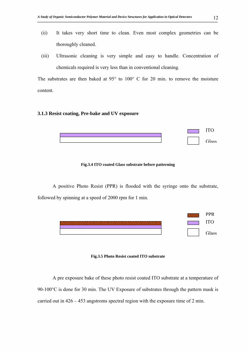
3.1.3 Resist coating, Pre-bake and UV exposure
Fig.3.4 ITO coated Glass substrate before patterning
A positive Photo Resist (PPR) is flooded with the syringe onto the substrate,
followed by spinning at a speed of 2000 rpm for 1 min.
Fig.3.5 Photo Resist coated ITO substrate
A pre exposure bake of these photo resist coated ITO substrate at a temperature of
90-100°C is done for 30 min. The UV Exposure of substrates through the pattern mask is
carried out in 426 – 453 angstroms spectral region with the exposure time of 2 min.
ITO
Glass
PPR
ITO
Glass
A Study of Organic Semiconductor Polymer Material and Device Structures for Application in Optical Detectors 13
3.1.4 Developing the resist and post baking
The exposed substrates are developed in developer (DI + KOH) followed by rinse in
DI water. The substrates are constantly agitated in these baths during this period. The
developed substrates are post baked at 120 – 130° C for 30 min.
Fig. 3.6 Hardened Photo resist after developing
3.1.5. ITO Etching
An ITO etchant consisting of 200 ml DI water, 60ml HCl and 15 ml HNO3 is used
for etching the ITO from the post baked substrate at a temperature between
55- 60°C for 6 -7 minutes.
Fig.3.7 Etched ITO substrate
3.1.6 Stripping of resist
After the etching, the resist is stripped using the acetone. The stripping of positive
resist becomes easier as compared to the stripping of negative photo-resist.
Fig. 3.8 Resist stripped and patterned ITO substrate
ITO
Glass
ITO
Glass
Hardened Resist
ITO
Glass
Hardened Resist
A Study of Organic Semiconductor Polymer Material and Device Structures for Application in Optical Detectors 14
3.1.7 Cleaning
The resist stripped substrates are rinsed in DI water and then cleaned with RCA 5:1:1
solution (200ml DI + 40 ml H2O2 + 40 ml NH4OH typically) by heating it for 30 min.
Rinsing the substrates in DI water , using ultrasonic shaking for 5 min and then drying
completes the cleaning process. The profile of patterned ITO, obtained from profilometer,
is shown in fig.3.9,
0 1000 2000 3000 4000 5000
0
500
1000
1500
2000
Ang
stro
m
Length in Micro Meters
Fig. 3.9: Profile of ITO obtained from Alpha Step 500 Surface profiler
3.2 Ozone treatment
The substrates after the cleaning are subjected to the ozone treatment for 15 min.
Studies suggest that treating the ITO surface with oxygen plasma / ozone increases the
work function of ITO, which will also lowers the hole barrier at anode [6-7] . The role of
ozone treatment is discussed in Appendix [A].
3.3 Coating of PEDOT-PSS layer & Vacuum Annealing
The PEDOT- PSS (Poly (3, 4-EthyleneDioxyThiophene, Poly (Styrene
Sulfonate)) is spun onto the ozone treated substrates for a thickness of the layer ~ 40nm.
Subsequently the substrates are vacuum annealed, such that water content is removed.
The role of PEDOT is discussed in Appendix [A].
A Study of Organic Semiconductor Polymer Material and Device Structures for Application in Optical Detectors 15
Fig. 3.10 PEDOT-PSS coated patterned ITO substrate.
3.4 Spin Coating of Active layer & Solvent removal
The active polymer layer is then spun onto vacuum annealed substrates at 1000 rpm
for 1 min. The substrates are then subjected to anneal in vacuum in order to ensure the
entire solvent removal.
Fig. 3.11 Vacuum annealed Polymer layer on patterned ITO substrates.
3.5 Cathode Deposition
Thermal evaporation is used for the deposition of the cathode layer. This evaporation
system consists of a diffusion pump backed by a rotary pump. The base pressure is of the
order of 4 x 10⁻⁶ to 3 x 10⁻⁶ mbar. The deposition is achieved by the application of current
through a filament of crucible. This then cause the filament or crucible to heat up and
allows the material to simply evaporate and is then deposited upon the polymer coated
ITO substrate.
ITOGlass
Annealed polymer layer Annealed PEDOT
ITO
Glass
PEDOT-PSS
A Study of Organic Semiconductor Polymer Material and Device Structures for Application in Optical Detectors 16
The width of cathode deposited is restricted to 2mm, using metal mask. Therefore
the active area has been 1mm x 2mm. The cathode used is Calcium/ Aluminum. Firstly,
calcium is deposited and then aluminum is evaporated for deposition. The 2 lines of
cathode deposited by using metal mask is shown in Fig.2.11
(a) Top View
(b) Side View
Fig. 3.12 Cathode deposited on the substrates.
3.6 Encapsulation
Since these metals have tendency to be unstable in air hence they have to be
encapsulated. The cathode deposited substrate is sealed with a glass plate using U-V
epoxy resin, which is then treated with ultra-violet light. The device is now ready for test.
Typical system configuration for the characterization is discussed in Appendix [B].
A Study of Organic Semiconductor Polymer Material and Device Structures for Application in Optical Detectors 17
Fig. 3.13 Glass Encapsulated ITO/PEDOT-PSS/Polymer Active Layer/Ca/Al Device.
Typical structure of Photo detector is shown in Fig 2.14. Each process in fabrication
has prominent effect on the device performance. Some of the modifications in fabrication
and their role on the device performance are studied in detailed in further chapters.
Fig. 3.14 Structure of Photodetector
+ -
ILLUMINATION
GLASS ITO PEDOT: PSS
POLYMER ACTIVE LAYER ALUMINUM
CALCIUM
Glass Encapsulation
Cathode deposited (Ca/Al)
ITO lines
A Study of Organic Semiconductor Polymer Material and Device Structures for Application in Optical Detectors
18
Chapter 4
Polymer Photodetector: Single Layer
4.1 Introduction
Organic thin film diodes made of polymer MEHPPV (Poly (2-Methoxy-5-(2’-
Ethyl-Hexyloxy)-1, 4-PhenylVinylene) are generally used as polymer light emitting
diodes (PLED’s). Very little photoresponse has been observed when the device structure
is optimized as LED’s. To increase the photoresponse, certain materials like C60 and its
derivatives are usually added to pure electroluminescent material. This chapter gives an
idea that even pristine MEHPPV can be used to fabricate a photodetector by optimizing
the device structure and processing conditions.
The Single layer polymer photodetector is fabricated using only polymer
MEHPPV as active layer. The chemical structure of MEHPPV is shown in Fig. 4.1
Fig. 4.1: Chemical Structure (the picture shows one repeat unit of polymer) and energy level diagram of MEHPPV
Vacuum level
LUMO
HOMO
2.8eV
5.2eV
χ
IP
A Study of Organic Semiconductor Polymer Material and Device Structures for Application in Optical Detectors
19
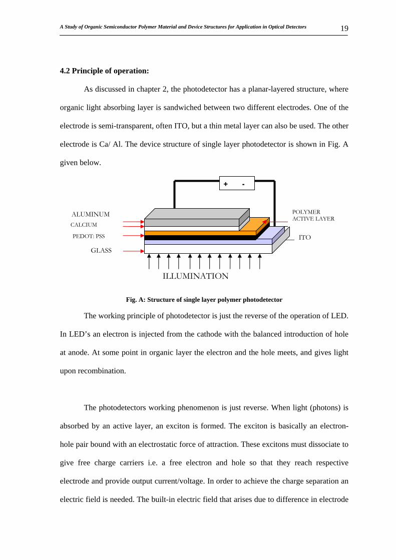
4.2 Principle of operation:
As discussed in chapter 2, the photodetector has a planar-layered structure, where
organic light absorbing layer is sandwiched between two different electrodes. One of the
electrode is semi-transparent, often ITO, but a thin metal layer can also be used. The other
electrode is Ca/ Al. The device structure of single layer photodetector is shown in Fig. A
given below.
Fig. A: Structure of single layer polymer photodetector
The working principle of photodetector is just the reverse of the operation of LED.
In LED’s an electron is injected from the cathode with the balanced introduction of hole
at anode. At some point in organic layer the electron and the hole meets, and gives light
upon recombination.
The photodetectors working phenomenon is just reverse. When light (photons) is
absorbed by an active layer, an exciton is formed. The exciton is basically an electron-
hole pair bound with an electrostatic force of attraction. These excitons must dissociate to
give free charge carriers i.e. a free electron and hole so that they reach respective
electrode and provide output current/voltage. In order to achieve the charge separation an
electric field is needed. The built-in electric field that arises due to difference in electrode
+ -
ILLUMINATION
GLASS ITO PEDOT: PSS
POLYMER ACTIVE LAYER ALUMINUM
CALCIUM
A Study of Organic Semiconductor Polymer Material and Device Structures for Application in Optical Detectors
20
work functions is found to be insufficient to split the photogenerated excitons. Thus with
external application of electric field this exciton dissociation is achieved. Fig 4.2 explains
the charge transfer in single polymer photodetector when the light is incident on it.
The Fig. 4.2 shows the energy level diagram of the single layer polymer
photodetector. The device is illuminated from the ITO side. When the photon strikes the
active layer of the device, an electron is promoted from the HOMO layer to the LUMO
energy level. This leaves a hole in HOMO layer, thus forming a neutral exciton on the
polymer chain. With the external bias provided, the dissociation of the exciton is
achieved. The electron travels to the higher electron affinity electrodes (Calcium and then
Aluminum), and then towards the positive terminal of the battery. Similarly the hole
travels towards the negative terminal of the battery through the PEDOT –PSS layer and
ITO. Thus generation, separation and transport of the charge takes place in the detector.
Fig 4.2: Energy level diagram. Upon irradiation an electron is promoted to LUMO leaving a hole behind in HOMO. Electrons are collected at Al electrode and holes at the ITO electrode.
A Study of Organic Semiconductor Polymer Material and Device Structures for Application in Optical Detectors
29
The polymer chains, dissolved in aromatic solvents (like Xylene Chlorobenzene,
1-2-Dichlorobenzene), have relatively open and straight conformation [11] with
maximum solute solvent interaction. The benzene rings of the conjugated polymer when
dissolved in the aromatic solvent aligns parallel to the surface, thus has planer
conformation as described in Fig. 4.8(a). It is expected that aromatic solvents can solvate
the π-conjugated segments better than the alkyl side chains [12]. This results in a
conformation which has better π-π stacking and subsequently better electrical conduction.
On the other hand, non-aromatic solvent (like chloroform) solvate the non-
conjugated segments i.e. alkyl side groups of the polymer. These alkyl side groups when
interacts among themselves, forms a tight coiled structure. This hinders the conjugation
length of the polymer backbone. Also the benzene ring structure of the polymers aligns
itself as perpendicular to the surface, with the non-conjugated group laying on the surface
as shown in Fig.4.8 (b). Thus the non aromatic solvents results in a polymer conformation
with a lower electrical conductivity
4.3.2 Variation in Device structure
The variation in the device structure is incorporated by varying the active layer
thickness. Now taking the best solvent i.e. Chlorobenzene (as discussed in section 4.3.1),
the active layer thickness can be varied by varying the spin speed or the by varying the
concentration of the polymer in the solvent. In this work, the concentration of the
polymers is varied. The concentration is reduced to 4mg of MEHPPV per cc of
Chlorobenzene. The reverse J-V and forward J-L-V characteristics of the devices are
shown in fig. 4.9(a), 4.9(b), 4.10(a) & 4.10(b) respectively for the thickness d = 70-80 nm
, d =150-160 nm.
A Study of Organic Semiconductor Polymer Material and Device Structures for Application in Optical Detectors
30
-4.0 -3.5 -3.0 -2.5 -2.0 -1.5 -1.0 -0.5 0.0
1E-8
1E-7
1E-6
1E-5
Reverse Voltage(V)
Cur
rent
Den
sity
(A/c
m2 )
Dark current density Photo current density Dark current(2) density
Chlorobenzened = 70 - 80 nm
Fig. 4.9(a): Reverse J -V characteristics of ITO/PEDOT/MEHPPV/Ca/Al device with active layer thickness of 70 -80nm
0 2 4 6 8-0.02
0.00
0.02
0.04
0.06
0.08
0.10
0.12
0.14
0.16
Cur
rent
Den
sity
(A/c
m2 )
Voltage(V)
d = 70 - 80 nm
Current Light Intensity
0
2
4
6
8
10
Light Intensity (a.u.)
Fig. 4.9(b): Forward J -L -V characteristics of ITO/PEDOT/MEHPPV/Ca/Al device with active layer thickness of 70 -80nm under forward bias.
A Study of Organic Semiconductor Polymer Material and Device Structures for Application in Optical Detectors
31
-8 -6 -4 -2 0
0
5
10
15
20
25
30
Rat
io (P
/D)
Voltage (V)
Maximum P/D = 29.51 at -0.8V
Chlrobenzene d = 70 -80 nm
Fig. 4.9(c): The ratio of Photo current density to dark current density plotted versus the applied voltage
-4.0 -3.5 -3.0 -2.5 -2.0 -1.5 -1.0 -0.5 0.0
1E-8
1E-7
1E-6
1E-5Chlorobenzened = 150 -160 nm
Dark current density Photo current density Dark current(2) density
Cur
rent
Den
sity
(A/c
m2 )
Reverse Voltage(V)
Fig. 4.10 (a): Reverse J-V characteristics of ITO/PEDOT/MEHPPV/Ca/Al device with
active layer thickness of 150 -160nm
A Study of Organic Semiconductor Polymer Material and Device Structures for Application in Optical Detectors
32
-2 0 2 4 6 8 10 12 14 16
0.00
0.01
0.02
0.03
0.04
0.05
d = 150-160nm
Cur
rent
Den
sity
(A/c
m2 )
Voltage(V)
Current Light Intensity
0.2
0.4
0.6
0.8
1.0
1.2
1.4
Light Intensity(a.u.)
Fig. 4.10(b): Forward J-L -V characteristics of ITO/PEDOT/MEHPPV/Ca/Al device with active layer thickness of 150 -160nm under forward bias
-8 -6 -4 -2 014.0
14.5
15.0
15.5
16.0
16.5
17.0
17.5
18.0
Rat
io (P
/D)
Voltage(V)
Chlorobenzened = 150-160nm
Maximum P/D = 17.89 at -3.1V
Fig. 4.10(c): The ratio of Photo current density to dark current density plotted versus the applied voltage
The above results are presented in Table 4.2. The characteristics in Fig 4.9(b) and
4.10(b) show that under forward bias the thinner device shows better performance than
the thicker one. The turn on voltage in thinner device is nearly 4V where as it is much
A Study of Organic Semiconductor Polymer Material and Device Structures for Application in Optical Detectors
33
higher ~ 8 -10V in thicker device. Also the light output in the thinner device is much
better. In the device with thicker active layer, the light intensity was found to be poor
even at 16V.
Active Layer Thickness 150-160 nm 70-80 nm
Reverse Bias (at -3.5V) Forward Bias Reverse Bias (at -3.5V) Forward Bias Dark Current density = -9.05 E-8 A/ cm2
Photo Current density = -1.51 E-6 A/ cm2
Turn on Voltage= ~ 8-10V Light intensity = poor
Dark Current Density= -2.913 E -6 A/ cm2 Photo Current Density= -2.22 E -5 A/ cm2
Turn on Voltage= ~ 4V Light intensity = Very Good
Ratio P/D = 16.8
Ratio P/D = 7.6
Table 4.2 Comparison of the devices with different active layer (MEHPPV) thickness
Comparing the characteristics in Fig.4.9 (a) and 4.10(a) it can be stated that as the
device active layer thickness increases there is an improvement in the characteristics of
the device. The dark current was found to be less in case of thicker device than in thinner
device.
Discussion:
The dark current is found to be higher in devices having thinner active layer. This
may be because of the higher surface roughness in the commercially obtained substrates.
The roughness of the substrate has been found to be 10.2 nm. It is preferred to have low
value of roughness in order to have low leakage currents.
The photo-response in the thinner device was found to be higher as compared to
the thicker device. This may be due to the better charge collection of electrodes. In larger
A Study of Organic Semiconductor Polymer Material and Device Structures for Application in Optical Detectors
34
active layer devices, the charges may be getting recombined before reaching the
electrodes.
The Fig. 4.9(c) and Fig. 4.10(c) represent the plot of ratio of photocurrent density
to the dark current density versus the applied voltage for the devices having active layer
thickness 70 -80 nm and 150 -160nm respectively. It is seen that if we bias the device at
-0.8V for the thinner device then the maximum ratio of P/D is obtained as 29.51 where as
in thicker device the bias voltage should be -3.1 V so as to get maximum ratio of 17.89.
It can be said that the device performance of the thinner device is good with respect to
irradiation than the thicker device except the leakage current values.
4.5 Summary:
The polymer MEHPPV is mostly used in the display like PLED applications.
When the device is optimized for the LED operation, very little photoresponse is
reported. The chapter shows that even pure MEHPPV can be used for the application in
photodetectors. This was achieved by changing the processing conditions and the active
layer thickness for the device. The processing conditions were varied by varying the
solvent in which the conjugated polymer MEHPPV is dissolved and the change in
polymer layer thickness changes the device structure.
The photoresponse of the detector using undoped MEHPPV polymer is still less
for the application in practical photodetectors. The response can be further improved with
the addition of the fullerene/polymer to the pure MEHPPV as discussed in next chapter.
A Study of Organic Semiconductor Polymer Material and Device Structures for Application in Optical Detectors
35
Chapter 5
Polymer Photodetector: Dispersed (Bulk)
Heterojunction
5.1 Introduction
The analysis of the pure conjugated polymer single layer device points out that
charge separation process in these monocompound layers is rather weak. To improve the
charge generation and separation the idea is to use two materials with different electron
affinities and ionization potentials. This will favour the exciton dissociation: the electron
will be accepted by the material with the larger electron affinity and the hole by the
material with the lower ionization potential.
Among the known electron acceptor materials Fullerene/ C60 and its derivatives
are very popular. One reason for the popularity of above class of n-type nanoparticles is
the lack of wide range of n-type (electron transporting) conjugated polymers. In this
work, one derivative of C60 i.e. PCBM, [6, 6]-Phenyl-C61 Butyric acid Methyl ester is
used. The chemical structure and energy level diagram of PCBM are shown in Fig. 5.1.
A Study of Organic Semiconductor Polymer Material and Device Structures for Application in Optical Detectors
36
Fig 5.1: Chemical Structure and energy level diagram of PCBM (HOMO – LUMO = 2.4eV)
In analogy to the classical p-n junction concept of electron donor material and
electron acceptor material forming bilayer structure [13] was quite of interest initially.
However for most of organic semiconductor the film thickness should be more than
100nm in order to absorb more light. It follows that thicker film layers increase light
absorption but only small fraction of the excitons will reach the interface and dissociate.
But the development of bulk heterojunction concept has opened up new research
directions. This bulk heterojunction concept is based on blends of the two organic
compounds, one with the donor properties and other with acceptor properties.
Device produced in a bilayer structure with a single interface between the electron
donor and acceptor had a low efficiency [14] because volume of the active layer where
efficient charge separation occurred was limited to a small fraction at the interface. An
early study shows that importance of close proximity of the polymer and fullerene for the
efficiency of the device. To overcome this problem, a device with a structure fabricated
from blend of MEHPPV and PCBM was incorporated [15].
Vacuum level
LUMO3.7eV
6.1eV
χIP
HOMO
A Study of Organic Semiconductor Polymer Material and Device Structures for Application in Optical Detectors
37
5.2 Fabrication details:
The two master solutions of MEHPPV & PCBM (8mg/cc) were prepared. The
blend solutions with defined concentrations were then obtained by mixing the two master
solutions in proper molecular ratio. The MEHPPV: PCBM blend films were spin cast
from blend solution at room temperature. The device configuration is ITO/PEDOT-
PSS/MEHPPV-PCBM/Ca/Al.
5.3 Principle of Operation:
By blending the material, the interface is distributed throughout the device as
shown in Fig 5.2. The difference in electron affinities creates driving force at the interface
between two materials that is strong enough to spilt photogenerated exciton. Hence,
generally all photogenerated excitons are likely to find an interface and split before
recombining [16].
Fig. 5.2: In blended device interface is distributed all over the device.
Figure shows one such interface.
A Study of Organic Semiconductor Polymer Material and Device Structures for Application in Optical Detectors
38
Fig.5.3: Absorption spectra of PCBM and C60. Absorption maximum for PCBM = 284 nm & 341nm. Courtesy: www.adsdyes.com In blended device, both electron accepting PCBM and a hole transporting
conjugated polymer are present throughout the bulk of the device, unlike the normal
bilayer device where the hole transport layer and electron transport layer are separately
defined. The absorption spectrum of PCBM is given in Fig. 5.3 and that of MEHPPV is
already given in Fig.4.11. Most of the absorption takes place in the conjugated polymer
layer. The excitons are generated with the absorption of the light. The dissociation of the
excitons into the electron and hole happens quickly in presence of the PCBM. Due to
higher electron affinity of PCBM than MEHPPV, electrons are attracted towards the
LUMO of PCBM, thus leaving a hole behind on MEHPPV polymer chains.
In the photodetector mode these charge carriers are drifted to the respective
electrode with the help of external electric field /voltage. Thus the charge transportation
becomes faster in the photodetector mode as compared to the photovoltaic mode where
no external bias is provided.
PCBM
C60
A Study of Organic Semiconductor Polymer Material and Device Structures for Application in Optical Detectors
39
5.4 Experiments, Results and Discussion:
While using the blend of MEHPPV and PCBM as photo absorbing layer, the
basic aim remains same, to get good device with low dark current and to achieve the
maximum photoresponse out of the device. To implement this, concentration of the
master materials in blend is varied. The three compositions used in this work are
MEHPPV: PCBM ratio being 1:1, 1:2 & 1:4 by weight in organic solvent.
Chlorobenzene as common organic solvent is used. Active layer thickness was 100-
110nm and device area used as 2 mm2. The corresponding devices were fabricated and
the J-V characteristics were taken in dark and illuminated environment shown in fig. 5.4,
5.5 and 5.6.
-4.0 -3.5 -3.0 -2.5 -2.0 -1.5 -1.0 -0.5 0.01E-9
1E-8
1E-7
1E-6
1E-5
1E-4
Dark Current density Photo Current density Dark Current density(2)
Cur
rent
Den
sity
(A /c
m2 )
Reverse Voltage(V)
MEHPPV :PCBM (1:1)
Fig.5.4(a): Reverse J-V characteristics of the device whose active layer has MEHPPV and PCBM are mixed in 1:1 proportion by weight in Chlorobenzene.
A Study of Organic Semiconductor Polymer Material and Device Structures for Application in Optical Detectors
40
-4.0 -3.5 -3.0 -2.5 -2.0 -1.5 -1.0 -0.5 0.0
0
500
1000
1500
2000
2500
Rat
io (P
/D)
Voltage(V)
MEH:PCBM (1:1)
Maximum P/D = 2324.07 at -0.6V
Fig.5.4(b) : The ratio of photo current density to dark current density versus applied voltage
-4.0 -3.5 -3.0 -2.5 -2.0 -1.5 -1.0 -0.5 0.0
1E-9
1E-8
1E-7
1E-6
1E-5
Dark Current density Photo Current density Dark Current density(2)
Reverse Voltage(V)
Cur
rent
Den
sity
(A/c
m2 )
MEHPPV :PCBM (1:2)
Fig.5.5(a) : Reverse J-V characteristics of the device whose active layer has MEHPPV and PCBM are mixed in 1:2 proportion by weight in Chlorobenzene.
A Study of Organic Semiconductor Polymer Material and Device Structures for Application in Optical Detectors
41
-4.0 -3.5 -3.0 -2.5 -2.0 -1.5 -1.0 -0.5 0.0
0
20
40
60
80
100
Rat
io(P
/D)
Voltage(V)
MEH:PCBM (1:2)
Maximum (P/D) = 89.14 at -3.5V
Fig.5.5(b) : The ratio of photo current density to dark current density versus applied voltage
-4.0 -3.5 -3.0 -2.5 -2.0 -1.5 -1.0 -0.5 0.0
1E-8
1E-7
1E-6
1E-5
Revese Voltage(V)
Cur
rent
Den
sity
(A/c
m2 )
MEHPPV:PCBM(1:4)
Dark Current density Photo Current density Dark Current density(2)
Fig.5.6 (a) : Reverse J-V characteristics of the device whose active layer has MEHPPV and PCBM are mixed in 1:4 proportion by weight in Chlorobenzene.
A Study of Organic Semiconductor Polymer Material and Device Structures for Application in Optical Detectors
42
-4.0 -3.5 -3.0 -2.5 -2.0 -1.5 -1.0 -0.5 0.0-20
0
20
40
60
80
100
120
140
160
Rat
io(P
/D)
Voltage(V)
MEH:PCBM(1:4)
Maximum (P/D) = 156 at -3.2 V
Fig.5.6(b) : The ratio of photo current density to dark current density versus applied voltage
For the ease of understanding the different results are being summarized in
following Table 5.1.
Current Density
(A / cm2) at -3.5V
MEHPPV: PCBM
(1:1)
MEHPPV: PCBM
(1:2)
MEHPPV: PCBM
(1:4)
Dark Current
Density -1.9036E-5 -2.004E-7 -2.495E-7
Photo Current
Density -8.103E-5 -1.7865E-5 -3.79965E-5
Ratio = P / D 4.25667 89.14671 152.29058
Table 5.1: Comparison of the ratio of photo current density to dark current density of the various devices made using different proportions of the master solution of MEHPPV and PCBM.
A Study of Organic Semiconductor Polymer Material and Device Structures for Application in Optical Detectors
43
The tabulated result shows that as the concentration of the PCBM with respect
MEHPPV is increased from 1:1 to 1:2, the ratio of photocurrent density to dark current
density increases by almost 20 times at -3.5V. Further, improvement in the ratio is
achieved by increasing the PCBM proportion to 4 times. As seen from the table, the
absolute value of the photocurrent is decreased as the MEHPPV proportion is decreased.
This has been shown that the function of the MEHPPV is light absorption and formation
of exciton (bound electron-hole pairs), and that of PCBM is the charge separation. It
seems that at blend ratio of 1:4, the MEHPPV acts as the limiting factor in charge
generation, and hence we are observing decrease in photocurrent.
The above improvement in photocurrent to dark current ratio is mainly coming
from the decrease in dark current. As the PCBM concentration is increased (in 1:2 and 1:4
proportions) in the blend the dark current is decreased as compared to the 1:1 proportion.
It suggests that PCBM is better capable of covering the surface roughness in comparison
to MEHPPV. There may be other reasons, which are yet to be explored.
The Fig. 5.4(b), Fig. 5.5(b) and Fig 5.6(b) represent the plot of ratio of photo
current density to dark current density versus applied voltage. The graph gives the
optimal value of the bias voltage for the device to get maximum of ratio (P/D). The ratio
in the device with MEHPPV: PCBM (1:1) is very high as 2324.07 at bias voltage of -
0.6V which is very less. If the leakage current in the device is decreased further at higher
voltages the device with blend proportion of 1:1 can be further explored.
A Study of Organic Semiconductor Polymer Material and Device Structures for Application in Optical Detectors
44
5.3.1 An OP-AMP Photodetector Circuit:
The device configuration where MEHPPV: PCBM blend ratio was kept 1:4 is
used in an op-amp photodetector circuit. The idea is to realize similar working of polymer
photodetector in place of inorganic photodetector for practical applications.
A photodetector produces current that is a linear function of the light intensity
incident on it. This current is converted to a voltage by an inverting op-amp in a current-
voltage converter mode. The output voltage depends on the input current. A simple light
sensing circuit consisting of a photodiode and an inverting op-amp is shown in Fig.5.7.
The anode terminal of the detector is connected to the negative terminal of a 6V supply.
To see the output, an organic LED or inorganic LED can be connected to the output pin
of the op-amp. Whenever light is incident on the detector, current is generated and then
converted into desired voltage through the op-amp in a current-voltage converter
configuration. This in turn helps to light up the LED connected to the output.
A Study of Organic Semiconductor Polymer Material and Device Structures for Application in Optical Detectors
45
The photographs of the practical demonstration are as shown in Fig.5.8 (a) & 5.8(b) Fig.5.8(a): Light is incident on the polymer photodetector (on left) and the organic polymer LED’s
are being driven through that using op-amp circuit. Fig. 5.8(b): Light is incident on the polymer photodetector (above right) and inorganic LED’s are being driven through that using op-amp circuit. 5.3.2 Rise Time Measurement: The rise time of the polymer photodetector is measured using the arrangement
shown in the Fig. 5.9. The photodetector was irradiated with the blue wavelength
(457nm). The blue light source is connected to the function generator generating a square
waveform of frequency 15 kHz having 50 % duty cycle. The photodetector is biased at -
6V. The output is taken across the resistance R. The value of R is varied from some ohms
to kilo ohms and corresponding rise time graphs are captured from the CRO. They are
shown in Fig. 5.10(a), 5.10(b), 5.10(c) and 5.10(d) respectively. The corresponding
values of R are also mentioned in these figures
A Study of Organic Semiconductor Polymer Material and Device Structures for Application in Optical Detectors
46
Fig. 5.9: Rise time measurement setup
Fig.5.10 (a): R = 680 ohms Fig.5.10(b): R = 2.7k ohms
Fig.5.10 (c): R = 6.2k ohms Fig.5.10 (d): R = 12k ohms
Reference Pulse
Output Pulse
Reference Pulse
Output Pulse
Reference Pulse
Output Pulse
Reference Pulse
Output Pulse
To X channel of CRO
Function Generator
To Y channel of CRO
To Y channel of CRO
Bias
PD
Light Sourc
R
A Study of Organic Semiconductor Polymer Material and Device Structures for Application in Optical Detectors
47
The rise time corresponding to each of the resistors used is being tabulated in the
Table 5.2 as shown.
Blue light wavelength used for the irradiation of photodetector = 457nm
Resistance Values Rise time values
680 Ω 450 ns
2.7 kΩ 1.915μs
6.2 kΩ 4.255 μs
12 kΩ 6.91 μs
Table 5.2: Rise time values of the photodetector for different values of resistor
The tabulated results are again expressed in graph as shown in Fig. 5.11. The rise
time data points are shown with the circular symbols. The linear fit for the data point is
obtained shown with the continuous line is the Fig. 5.11.
Fig. 5.11: Rise time Versus Resistance characteristics.
0 2000 4000 6000 8000 10000 12000
0.0
1.0x10⁻⁶
2.0x10⁻⁶
3.0x10⁻⁶
4.0x10⁻⁶
5.0x10⁻⁶
6.0x10⁻⁶
7.0x10⁻⁶
Data points Linear Fit
Ris
e tim
e (s
)
Resistance (ohms)
A Study of Organic Semiconductor Polymer Material and Device Structures for Application in Optical Detectors
48
The equation (5.1) obtained from the graph for the linear fit is given as τ = 0.326 x 10⁻⁶ + 0.566 x 10⁻⁹ R (5.1) where τ is the total delay time of the device and R value of resistance connected with the
device. Thus comparing it with the equation (5.2) we get,
τ = τint + C R (5.2) Capacitance value C = 0.566 nF and intrinsic time delay τint = 0.32 μsec.
The capacitance value can also be calculated theoretically with the equation (5.3) as given
below
C = (A εo εR) / d (5.3)
Where A is the area of the device, εo is the free space permittivity, εR being relative
permittivity of the material and d is the active layer thickness. Inserting the values we get
C = (0.02 cm2 x 8.854 x 10-14 F/cm x 3) / 1000 x 10-8 cm
C = 0.53 x 10⁻⁹ F
C = 0.53 nF
The calculated value of the capacitance from the rise time measurement is 0.566nF and
the theoretical value of the capacitance is the 0.53 nF. Thus calculated value of the
capacitance shows excellent agreement with theoretical capacitance of the device.
5.4 Summary:
The fullerene derivative PCBM was added to the pure conjugated polymer
MEHPPV to get the better photoresponse. Generally the evaporation of the C60 material
over the MEHPPV is done to get the hetero-structured device. To get the blend of the
polymer and fullerene material, a derivative, PCBM was found suitable. The PCBM was
soluble in common organic solvent at room temperature. The concentration of the PCBM
A Study of Organic Semiconductor Polymer Material and Device Structures for Application in Optical Detectors
49
in the blend of MEHPPV and PCBM found to affect the device characteristics of the
device with respect to light. With the higher concentration of PCBM in blend, the ratio of
photo current density to dark current density was improved.
The OP_AMP photodetector circuit shows the physical demonstration of the
polymer photodetector in the circuit. The inorganic as well as organic LED’s were driven
by the polymer photodetector. The transient response measurement was done on the
photodetector with different values of load resistors. The rise time measured at 650 Ω
load was 450 ns and the capacitance value calculated was 0.566 nF.
A Study of Organic Semiconductor Polymer Material and Device Structures for Application in Optical Detectors
50
Chapter 6 Conclusion and Future Work
In this work photodetectors using polymer material having good electrical and
optical characteristic have been demonstrated. The pure conjugated polymer MEHPPV
and MEHPPV (polymer): PCBM (carbon nano particle) blend have been successfully
utilized as photo absorbing layer in the organic detector.
The pure conjugated polymer MEHPPV is known for its electroluminescence
effect. When the device conditions using electroluminescence layer are optimized for
LED operation, very little photoresponse is observed. The optimizations have been done
in this work, to get low dark current and better photoresponse. It is found that the
variation of the solvent leads to better solubility and film formation. Devices were
fabricated using different organic solvents like chloroform, 1-2-Dichlorobenzene, Xylene
and Chlorobenzene. Out of all these it was found that aromatic solvent, Chlorobenzene,
gives best results in terms of low leakage and film uniformity. Further the variation of the
active layer thickness was done to see the effect on the device characteristics. The device
leakage current was reduced when the active layer thickness was higher; this in turn
increased the ratio of the photocurrent density to dark current density.
Thus, it is shown that even pure conjugated polymer can be used as photodetector
with the optimization of the processing conditions. To further improve the photoresponse
of the device the studies were carried out using MEHPPV and PCBM as blend.
A Study of Organic Semiconductor Polymer Material and Device Structures for Application in Optical Detectors
51
The fullerene /C60 derivative (PCBM) was added to the pure polymer MEHPPV.
The configuration of the device was ITO/PEDOT-PSS/MEHPPV-PCBM/Ca/Al. The
variation in the concentration of the PCBM in the blend of the MEHPPV and PCBM
leads to changes in the response of the device towards light. The devices were fabricated
using different ratios of the MEHPPV and PCBM like 1:1, 1:2 & 1:4. It is found that the
device with higher concentration of the PCBM with respect to the MEHPPV (MEHPPV:
PCBM = 1:4) was found to be the best device among all in terms of the ratio of
photocurrent density to the dark current density.
The transient response measurement of the device with MEHPPV: PCBM (1:4) as
photo-absorbing layer was made at different resistive loads. The rise time was measured
as 450 nano-seconds at 680Ω and the calculated capacitance value was 0.53nF.
Future Work:
1. The choice of polymers other than MEHPPV like MDMO-PPV, P3HT can be
employed. Also the electron acceptor material other than carbon nano particles
like CNPPV (other conjugated polymers) can be studied.
2. The operating region of the detector can further be extended to the near IR using
suitable dyes.
3. The photoresponse from the pure conjugated polymers MEHPPV needs better
understanding in terms of charge generation and charge separation phenomenon.
4. The same configuration of MEHPPV: PCBM (1:4) can be used under the
photovoltaic mode also. Further studies are needed in this direction.
A Study of Organic Semiconductor Polymer Material and Device Structures for Application in Optical Detectors
52
BIBLIOGRAPHY
[1] C.W. Tang and S. A.Vanslyke, Appl. Phys. Lett., 1987, 51, 913.
[2] S. Forrest, P.Burrows & M.Thompson, featured article, IEEE Spectrum online,
[14] K. M. Coakley, M. D. McGehee, Chem. Mater. (Review), 2004, 16(23), 4533.
[15] G. Yu, J. Gao, J.C. Hummelen, F. Wudl, A.J. Heeger, Science, 1995, 270, 1789.
[16] C. J. Brabec, Solar Energy Material and Solar Cells, 2004, 83, 273.
[17] C.C. Wu, C. I. Wu et al., Appl. Phys. Lett., 1997, 70(11), 1348.
[18] S.Y. Kim et al., J. Appl. Phys., 2004, 95, 2560.
A Study of Organic Semiconductor Polymer Material and Device Structures for Application in Optical Detectors
53
Appendix [A]
Surface Treatment of Tin doped Indium
Oxide (ITO)
ITO finds itself suitable for electrode (anode) contact in most of the organic
devices due to its high conductivity, transparency to visible light and higher work
function (~ 4.7 eV). The device usually consists of a sandwich structure with organic thin
film deposited onto ITO (anode) coated glass substrate and covered by patterned top
metal electrode (cathode) contact.
The organic thin film is in direct contact with the ITO and work function of the
ITO is sensitive to the surface conditions hence device characteristics gets affected. To
minimize the problems, the properties of organic material/ ITO surface can be changed or
an intermediate stabilization layer with proper carrier transport characteristics between
ITO and active layer can be introduced.
The two treatments to modify the surface of ITO implemented in this work are
(a) treating the ITO surface by UV-Ozone.
(b) introduction of intermediate layer of PEDOT- PSS between ITO and
active layer.
A Study of Organic Semiconductor Polymer Material and Device Structures for Application in Optical Detectors
54
(a) Role of UV-ozone treatment On ITO surface
Since the ITO films are initially patterned using photolithography process,
it is said that there are certain organic contamination on the surface along with
remnant carbon atoms which decreases the charge transfer across the interface.
Studies suggest modifying the ITO surface by various methods, such as
chemical treatment, oxygen plasma and UV-ozone treatment. Among such
surface treatments, UV-ozone treatment is one of the most effective techniques
which in turn increase the work function of the ITO surface [17, 18].
The ITO samples are placed in UV treatment chamber after the proper
cleaning. UV was irradiated using a low- pressure mercury lamp with the
wavelength of 254nm. Oxygen was flowed into the chamber. UV radiations are
absorbed by oxygen, changing it to ozone and nascent oxygen. It is thought that
carbon on ITO surface was oxidized into C-O or C=O during UV –Ozone
treatment followed by pumping out from the UV chamber by using a vacuum
pump.
A Study of Organic Semiconductor Polymer Material and Device Structures for Application in Optical Detectors
55
(a) (b)
Fig : A.1 Typical band structure (a) Before ozone treatment ITO( ~4.7 eV) & HOMO of MEHPPV( ~5.2 eV) (b) After ozone treatment ITO (~4.9eV) & HOMO of MEHPPV (~5.2eV).
(b) Role of PEDOT-PSS layer
Another surface treatment includes introduction of PEDOT-PSS (Poly (3, 4-
ethylenedioxythiophene) poly (styrenesulfonate)) layer between ITO and
MEHPPV. The PEDOT-PSS layer performs dual functions in the device
(i) It solves the problem of the inconsistent ITO surface since it acts as a
smoothening interface between rough ITO and active MEHPPV layer
thus preventing shorts between +ve and –ve electrodes, especially if
active layer is thin.
(a) (b)
Fig: A.2 (a) when PEDOT-PSS layer is not present, can lead to short (b) PEDOT-PSS layer is present, thus avoiding short
HOMO Φh Ef
+
ITO MEHPPV
LUMO
Ef Φh
ITO MEHPPV
LUMO
HOMO
A Study of Organic Semiconductor Polymer Material and Device Structures for Application in Optical Detectors
56
(ii) It has higher work function than (~5.1 eV) ITO which gives better
alignment of work function with the homo level of active layer for the
polymer.
Fig: A.3 Typical band structure showing alignment of workfuction with the addition of PEDOT –PSS layer.
A Study Of Organic Semiconductor Polymer Material and Device Structures For Application In Optical Detectors
57
Appendix [B]
Programming KEITHLEY SMU and
DMM
The Polymer Devices fabricated are characterized using computer interfaced
Keithley 236 High Voltage Source Measure Unit (SMU) and Keithley 196 Digital Multi-
Meter (DMM). While measuring the photo detector characteristics only SMU is used with
the broad light source with ~ 12 mW power output. Setup is shown as shown in Fig [B.2].
For characterization of polymer LED’s DMM and SMU are used, Fig [B.1] showing the
setup.
Fig. B.1:Typical system configuration to characterize PLED (PD is photodetector).
Keithley 236 SMU
PLED
PD
Keithley 196 DMM
Bias
Data Acquisition Computer
GPIB
A Study Of Organic Semiconductor Polymer Material and Device Structures For Application In Optical Detectors
58
Fig. B.2: Typical system configuration to characterize photodetector.
The Source measure unit and DMM are interfaced to computer using IEEE-488
Bus. These instruments are programmed using Lab VIEW 5.1 software. The experimental