Science and Technology of Advanced Materials TOPICAL REVIEW A study of the synthetic methods and properties of graphenes To cite this article: C N R Rao et al 2010 Sci. Technol. Adv. Mater. 11 054502 View the article online for updates and enhancements. You may also like Water Phase Synthesis Method of CuInS 2 Nanoparticles and Its Application for Photovoltaic Device Hideyuki Takahashi, Mitsuo Goto and Shun Yokoyama - Ammonia Synthesis at Intermediate Temperatures from N 2 and Steam in Solid- State Electrochemical Cells Using Cesium Hydrogen Phosphate Based Electrolytes Ryuji Kikuchi, Shota Kishira, Geletu Qing et al. - Shape Transition and Growth of Co x Fe (1-x) Alloy Nanocrystals By Electrochemical Deposition Kimoon Park, Sanghwa Yoon and Bongyoung Yoo - Recent citations Thermodynamic and magnetocaloric properties of a triple-layer graphene-like structure Lei Sun et al - Intrinsically stretchable transparent electrodes based on silver- nanowire–crosslinked-polyacrylate composites Weili Hu et al - Graphene: chemical approaches to the synthesis and modification E D Grayfer et al - This content was downloaded from IP address 116.49.15.201 on 11/12/2021 at 13:29
Transcript
Science and Technology ofAdvanced Materials
TOPICAL REVIEW
A study of the synthetic methods and properties ofgraphenesTo cite this article: C N R Rao et al 2010 Sci. Technol. Adv. Mater. 11 054502
View the article online for updates and enhancements.
You may also likeWater Phase Synthesis Method of CuInS2Nanoparticles and Its Application forPhotovoltaic DeviceHideyuki Takahashi, Mitsuo Goto andShun Yokoyama
-
Ammonia Synthesis at IntermediateTemperatures from N2 and Steam in Solid-State Electrochemical Cells Using CesiumHydrogen Phosphate Based ElectrolytesRyuji Kikuchi, Shota Kishira, Geletu Qinget al.
-
Shape Transition and Growth of CoxFe(1-x)Alloy Nanocrystals By ElectrochemicalDepositionKimoon Park, Sanghwa Yoon andBongyoung Yoo
-
Recent citationsThermodynamic and magnetocaloricproperties of a triple-layer graphene-likestructureLei Sun et al
-
Intrinsically stretchable transparentelectrodes based on silver-nanowire–crosslinked-polyacrylatecompositesWeili Hu et al
-
Graphene: chemical approaches to thesynthesis and modificationE D Grayfer et al
-
This content was downloaded from IP address 116.49.15.201 on 11/12/2021 at 13:29
A study of the synthetic methodsand properties of graphenesC N R Rao1,2, K S Subrahmanyam1, H S S Ramakrishna Matte1,B Abdulhakeem1, A Govindaraj1,2, Barun Das1,2, Prashant Kumar1,Anupama Ghosh1,2 and Dattatray J Late1
1 Chemistry and Physics of Materials Unit, International Centre for Materials Science, New ChemistryUnit and CSIR Centre of Excellence in Chemistry, Jawaharlal Nehru Centre for Advanced ScientificResearch, Jakkur PO, Bangalore 560 064, India2 Solid State and Structural Chemistry Unit, Indian Institute of Science, Bangalore 560012, India
Received 10 June 2010Accepted for publication 10 August 2010Published 27 October 2010Online at stacks.iop.org/STAM/11/054502
AbstractGraphenes with varying number of layers can be synthesized by using different strategies.Thus, single-layer graphene is prepared by micromechanical cleavage, reduction ofsingle-layer graphene oxide, chemical vapor deposition and other methods. Few-layergraphenes are synthesized by conversion of nanodiamond, arc discharge of graphite and othermethods. In this article, we briefly overview the various synthetic methods and the surface,magnetic and electrical properties of the produced graphenes. Few-layer graphenes exhibitferromagnetic features along with antiferromagnetic properties, independent of the method ofpreparation. Aside from the data on electrical conductivity of graphenes and graphene-polymercomposites, we also present the field-effect transistor characteristics of graphenes. Onlysingle-layer reduced graphene oxide exhibits ambipolar properties. The interaction ofelectron donor and acceptor molecules with few-layer graphene samples is examined indetail.
The discovery of the fascinating properties of single-layergraphene (SLG) has generated much interest in the physicaland materials sciences [1–4]. Graphene exhibits an ambipolarelectric field effect along with ballistic conduction of chargecarriers [5], integer quantum Hall effect at room temperature,fractional quantum Hall effect at low temperatures [6–8] andhigh elasticity [9]. As investigations of single, bi-, tri- andfew-layer graphenes (n < 10) are being pursued, it is useful toclassify graphenes by the number of layers. After the initial
studies conducted on SLG prepared by micromechanicalcleavage, graphenes containing varying number of layers havebeen produced using diverse strategies [2, 4, 10]. There arereports on some of the properties of few-layer graphenes, butonly a few studies document the changes brought about by thevariation in the number of layers. Furthermore, well-definedprocedures are still lacking for the synthesis of grapheneswith the desired number of layers. In this article, we discussthe methods used to produce graphenes with varying numberof layers and then examine their surface, magnetic andelectrical properties. The electrical properties pertain to pure
graphenes as well as to their composites with polymers. Thecharacteristics of field-effect transistors formed with differentgraphene samples are also compared.
Graphene is characterized by a variety of techniques.In particular, transmission electron microscopy (TEM) andatomic force microscopy (AFM) are essential for determiningthe number of layers and other structural features. Among thespectroscopic techniques, Raman scattering is very effectivein investigations of graphene. Whereas carbon nanotubes canbe characterized with optical absorption and luminescence,Raman spectroscopy is the only optical tool available forstructural investigations of graphene, providing informationabout the quality and number of layers in a given sample.The G-band (around 1580 cm−1) in the Raman spectra issensitive to doping and other effects. The D-band (around1340 cm−1), which is a defect-related band, also provides asignature of the quality of the graphene. SLG shows a strongG-band and a very weak D-band, but the D-band strengthenswith the increase in the number of layers. The 2D-band(∼2600 cm−1), which appears in both single-layer andfew-layer graphenes, is sensitive to both the number of layersand doping. Here, we present data from Raman spectroscopyand other characterization techniques wherever necessary.In the discussion of properties, we compare the featuresexhibited by graphenes with different number of layers andprepared by different methods.
2. Synthesis methods
2.1. Single-layer graphene
Single-layer graphene is generally prepared bymicromechanical cleavage from highly ordered pyrolyticgraphite (HOPG) [11]. In this procedure, a layer is peeledoff the HOPG crystal with Scotch tape and transferred onto asilicon substrate. A popular chemical method to prepare SLGinvolves reduction of single-layer graphene oxide (SGO)dispersion in dimethlyformamide (DMF) with hydrazinehydrate [12]. Graphite oxide (GO) [5, 13] readily forms astable colloidal suspension in water, and the suspension issubjected to ultrasonic treatment (300 W, 35 kHz) to produceSGO. The SGO suspension (0.3 mg ml−1) in a mixture ofwater and DMF is treated with hydrazine hydrate at 80 ◦Cfor 12 h [12]. This yields a black suspension of reducedgraphene oxide (RGO) in DMF/H2O. An additional amountof DMF is then added to stabilize the suspension. The thusprepared single-layer graphene (RGO) differs, however,from the SLG obtained by micromechanical cleavage ofgraphite or other means by that RGO contains some residualoxygen. Gram quantities of single-layer graphene can beobtained by a solvothermal procedure using sodium andethanol [14]. Exfoliation of graphite in N -methyl pyrrolidoneor surfactant/water solution employing ultrasonication alsoyields stable SLG dispersions [15, 16].
SLG films are produced on the Si-terminated (0001)face of single-crystal 6H-SiC by the thermal desorption ofSi [17–19]. In this procedure, the substrates are subjectedto electron bombardment in ultrahigh vacuum at 1000 ◦C to
remove oxide contaminants and then heated to temperaturesranging from 1250 to 1450 ◦C for 1–20 min. The formation ofcarbon films by cooling Ni foils saturated with carbon at hightemperatures was studied by Blakely and co-workers [20–22].Recently, SLG has been prepared by the decomposition ofhydrocarbons on films or sheets of transition metal such asNi, Cu, Co and Ru [23]. We have employed this methodto generate graphene layers on different transition metalsubstrates by decomposing a variety of hydrocarbons such asmethane, ethylene, acetylene and benzene. We found that thenumber of layers varies with the hydrocarbon and reactionparameters. In our experiments, nickel and cobalt foils withthicknesses of 0.5 and 2 mm, respectively, were used ascatalysts. These foils were cut into 5 × 5 mm2 pieces andpolished mechanically, and the chemical vapor deposition(CVD) was carried out by decomposing hydrocarbons at atemperature in the range 800–1000 ◦C. By employing a nickelfoil, CVD was carried out by passing methane (60–70 sccm)or ethylene (4–8 sccm) along with a high flow of hydrogen ofabout 500 sccm at 1000 ◦C for 5–10 min. When using benzeneas the hydrocarbon source, benzene vapor diluted with argonand hydrogen was decomposed at 1000 ◦C for 5 min. On acobalt foil, acetylene (4 sccm) and methane (65 sccm) weredecomposed at 800 and 1000 ◦C, respectively. In all theseexperiments, the metal foils were cooled gradually after thedecomposition. The produced graphene layers were difficultto remove from the metal surface, however, and this is adrawback of the CVD method.
Figure 1 shows high-resolution TEM images of graphenesheets obtained by CVD on a nickel foil. Figures 1(a)–(c)show graphenes obtained by the thermal decomposition ofmethane and benzene, respectively, on the nickel foil. Theinsets in figures 1(a) and (c) show selected area electrondiffraction (SAED) patterns. Figure 1(b) clearly reveals theedge of the graphene sheet. All these graphene samplesexhibit the G-band at 1580 cm−1 and the 2D-band around2670 cm−1 with a narrow linewidth of 30–40 cm−1. Thenarrow linewidth and relatively high intensity of the 2D-bandconfirm that these Raman spectra correspond to 1–2 layergraphenes [23]. In figures 2 and 3, we plot the Raman spectrarecorded from different graphene samples produced by CVD.The Raman spectra of graphene grown on nickel by thethermal decomposition of methane, ethylene and benzene,particularly the first two hydrocarbons, show an intense2D-band, a weaker G-band and hardly any D-band (seefigures 2(a) and (b)), and are clearly indicative of SLGs [23].Figures 3(a) and (b) show the Raman spectra of grapheneprepared on cobalt by the thermal decomposition of methaneand acetylene, respectively; the spectrum in (b) resembles thatof SLG.
2.2. Few-layer graphene
An important method to prepare few-layer graphene is thermalexfoliation of graphite oxide at high temperatures [13, 24–26].In this procedure, graphite oxide (0.2 g) is placed in analumina boat and inserted into a long quartz tube sealedat one end. The sample is purged with Ar for 10 min,
Figure 1. TEM images of graphene prepared by the thermal decomposition of (a, b) methane (70 sccm) and (c) benzene (Ar passed throughbenzene at a flow rate of 200 sccm), at 1000 ◦C on a nickel sheet. Insets in (a) and (c) show electron diffraction patterns from thecorresponding graphene sheets.
1250 1500 1750 2000 2250 2500 2750750
1500
2250
3000
3750
Inte
nsity
(a.
u)
1250 1500 1750 2000 2250 2500 2750
1000
2000
3000
4000
Inte
nsity
(a.
u)
1250 1500 1750 2000 2250 2500 2750
1200
1250
1300
1350
1400
1450
Inte
nsity
(a.
u)
Raman Shift (cm-1) Raman Shift (cm-1)
Raman Shift (cm-1) Raman Shift (cm-1)
1250 1500 1750 2000 2250 2500 2750
1050
1400
1750
2100
2450
2800In
tens
ity (
a.u)
(a) (b)
(d)(c)
Figure 2. Raman spectra of graphene prepared by the thermal decomposition of hydrocarbons on a nickel sheet: (a) methane (70 sccm) at1000 ◦C, (b) ethylene (4 sccm) at 900 ◦C, (c) benzene (argon passed through benzene at a flow rate of 200 sccm) at 1000 ◦C, (d) benzene(argon passed through benzene at a flow rate of 400 sccm) at 1000 ◦C.
and then the tube is quickly inserted into a tube-furnacepreheated to 1050 ◦C and held in the furnace for 10 min.The graphene obtained by this procedure has few layersand is called exfoliated graphene (EG). Another methodof preparing few-layer graphene is by reacting SGO in
water with hydrazine hydrate at the refluxing temperatureor by microwave treatment (EG-H) [2, 27]. In this method,hydrazine hydrate (1 mM) is added to 100 ml of stableaqueous exfoliated graphene oxide solution (1 mg ml−1) andrefluxed for 24 h. The reduced graphite oxide turns black
Figure 3. Raman spectra of graphene prepared by the decomposition of (a) methane (64 sccm) at 1000 ◦C and (b) acetylene (4 sccm) at800 ◦C on a cobalt sheet.
20 nm50 nm
20 nm5 nm
(b)(a)
(d)(c)
Figure 4. TEM images of (a) DG-1650, (b) DG-1850, (c) DG-2050 and (d) DG-2200 samples. The sample number indicates thetemperature of transformation in ◦C.
and precipitates at the bottom of the flask. The resultingprecipitate is filtered and washed with water and methanol.Instead of hydrazine hydrate, one can also use ethylene glycol
as a reducing agent to prepare few-layer graphene (EG-H(G)).In this procedure, the homogeneous mixture of 25 ml ofexfoliated graphene oxide and 2 ml of ethylene glycol is
Figure 5. Histograms of height profile and lateral dimensions of (a) DG-1650 and (b) DG-2200 samples obtained from the analysis ofAFM images.
placed in a 50 ml Teflon-lined bomb. The sealed autoclave iskept in an oven at 170 ◦C for 24 h under autogenous pressureand allowed to gradually cool to room temperature. Theproduct is washed with water and ethanol.
Few-layer graphene can be prepared by heatingnanodiamond in an inert or reducing atmosphere (DG) [25,28] and the effect of temperature on the product hasbeen studied by Enoki and co-workers [28, 29]. Wehave examined this procedure in detail. We first treatednanodiamond particles by soaking in concentrated HCl toavoid contamination with magnetic impurities. We thenheated 100 mg of pristine nanodiamond powder (particle size4–6 nm, Tokyo Diamond Tools, Japan) placed in a graphitecontainer in a graphite furnace in a helium atmosphere atdifferent temperatures (1650, 1850, 2050 and 2200 ◦C) for1 h. These samples are designated as DG-1650, DG-1850,DG-2050 and DG-2200, respectively, and figure 4 showstheir TEM images. Figure 5 shows the histograms of thenumber of layers and of the lateral dimension of the DG-1650and DG-2200 samples obtained from AFM data. There isa slight increase in the number of layers and a decrease inlateral dimensions after heating at 2200 ◦C. Raman spectraof DG-1650 and DG-2200 samples in figure 6 show thecharacteristic D-, G- and 2D-bands of graphene at 1340, 1580
and 2680 cm−1, respectively. The D-band is quite intense inthe DG samples.
We have discovered that arc evaporation of graphitein the presence of hydrogen yields graphene (HG) withexclusively 2–3 layers, although the flakes are relatively small(100–200 nm) [30]. This process relies on the knowledgethat the presence of H2 during the arc discharge terminatesthe dangling carbon bonds with hydrogen and prevents theformation of closed structures. To prepare HG, direct currentarc discharge of graphite evaporation was carried out in awater-cooled stainless steel chamber filled with a mixtureof hydrogen and helium in different proportions, withoutusing any catalyst. The partial pressures of H2 and Hewere H2 (70 torr)-He (500 torr), H2 (100 torr)-He (500 torr),H2 (200 torr)-He (500 torr) and H2 (400 torr)-He(300 torr). Ina typical experiment, a graphite rod (Alfa Aesar, 99.999%purity, 6 mm in diameter and 50 mm in length) was used asthe anode and another graphite rod (13 mm in diameter and60 mm in length) was used as the cathode. The dischargecurrent was in the 100–150 A range, with a maximumopen-circuit voltage of 60 V [31]. Figure 7 shows typical TEMand AFM images of a produced sample. An important aspectof the arc discharge method is its use in doping graphenewith boron or nitrogen [32]. Boron-doped and nitrogen-doped
Figure 6. Raman spectra of (a) DG-1600 and (b) DG-2200 samples.
graphenes (B-HG and N-HG) were obtained by carryingout the discharge in the presence of H2+ diborane and H2+(pyridine or ammonia), respectively. Table 1 summarizes thedifferent methods of graphene synthesis and the number oflayers obtained. In spite of the many advances made in thelast four years, controlled synthesis with a desired number oflayers remains a challenge.
3. Surface properties of few-layer graphenes
Single-layer graphene is theoretically predicted to have alarge surface area of 2600 m2 g−1 [33]. We have measured thesurface properties of few-layer graphene samples prepared bydifferent methods. The Brunauer, Emmett and Teller (BET)surface area was typically in the range of 270–1550 m2 g−1,
approaching the value of single-layer graphene for somesamples [34]. The surface area varies as EG > DG > EG-H >HG. These high surface area samples might enable the storageof hydrogen. Hydrogen storage reaches 3 wt% at 100 bar and300 K and the uptake varies linearly with the surface area [34].Theoretical calculations show that SLG can accommodate up
Table 1. Synthetic methods and the number of layers in graphenes.
Synthetic method No. of layers
Micromechanical cleavage from graphite 1Solution phase exfoliation of graphite 1Epitaxial growth 1Chemical vapor deposition (CVD) 1Solvothermal synthesis 1Reduction of single-layer 1
graphene oxide (RGO)Arc evaporation of graphite in H2(HG)a 2–3Thermal exfoliation of graphite oxide (EG) 2–7Chemical reduction of exfoliated 2–6
graphene oxide (EG-H)Conversion of nanodiamond (DG) 4–8
aNitrogen-doped and boron-doped HG samples (N-HG andB-HG) have been prepared by introducing N- andB-containing molecules in the arc discharge.
to 7.7 wt% hydrogen, whereas bi- and trilayer graphenes canhave an uptake of ∼2.7 wt % and that the H2 molecules attachto the graphene surface in an alternating end-on and side-onfashions. The CO2 uptake of few-layer graphenes at 1 atm and195 K is around 35 wt%. Calculations suggest that SLG canhave a maximum uptake of 37.9 wt% CO2 and that the CO2
molecules reside parallel to the graphene surface [34].
4. Magnetic properties of few-layer graphenes
There were a few studies on the magnetic properties ofnanographite particles, which demonstrate the importance ofthe edge states arising from the nonbonding electrons [35–37].It was pointed sometime ago that edges in graphene ribbonsplay a crucial role in determining the electronic structure [35].Nanographite particles exhibit unusual magnetic propertiesincluding spin-glass behavior and magnetic switchingphenomena [38–40]. Bilayer graphene is predicted to beferromagnetic [41]. Hydrogenated nanographite is alsopredicted to show spontaneous magnetism [42]. Themagnetic properties of nanographite were reviewed by Enokiet al [38–40] and the main message is that the edge statesand the adsorbed or intercalated species affect the magneticproperties. By carrying out first-principles density functionalcalculations, Lee et al [43] have shown the existence of aferromagnetically ordered ground state in the zigzag edgesof graphene. Zigzag edges longer than 3–4 repeat units arepredicted to be magnetic, irrespective of whether the edgesare regular or irregular [44, 45].
We have studied the magnetic properties of differentgraphene samples. Magnetization measurements werecarried out with a vibrating sample magnetometer in aphysical property measurement system (PPMS, QuantumDesign, San Diego, CA, USA). All the graphene samplesshow a divergence between the field-cooled (FC) andzero-field-cooled (ZFC) curves, which starts at around 300 Kand disappears upon the application of the magnetic fieldof 1 T (for typical data from EG material see figure 8).The divergence between the FC and ZFC curves in thegraphene samples is similar to that in magnetically frustratedsystems. The Curie–Weiss temperatures obtained from the
high-temperature inverse susceptibility data were negative inall these samples, indicating the presence of antiferromagneticinteractions. Interestingly, we observe well-defined maximain the magnetization at low temperatures, the maximabecoming prominent in the data recorded at 1 T. Suchmagnetic anomalies are found when antiferromagneticcorrelations compete with ferromagnetic order. It is possiblethat the data correspond to the coexistence of differenttypes of magnetic states [46]. The ferromagnetic clustersin such a case would not be associated with a well-definedglobal ferromagnetic transition temperature. This behavior issimilar to that of microporous carbon and the members of therare-earth manganite family with the formula RE1−x Ax MnO3
(RE = rare-earth, A = alkalineearthelement) [47–50]. Recent
theoretical calculations do indeed predict the presence ofantiferromagnetic states in the sheets and ferromagneticstates at the edges of graphene [51]. All the graphene samplesshow magnetic hysteresis at room temperature (figure 9).In DG samples, we observe a systematic decrease inmagnetization with increasing preparation temperature. Thus,in DG-1650, the saturation magnetization (Ms), remnantmagnetization (Mr) and coercive field (Hc), are 0.04 emu g−1,0.0015 emu g−1 and 41 Oe, whereas in DG-2200, theyare 0.02 emu g−1, 0.001 emu g−1 and 213 Oe, respectively.Among all the samples, HG shows the best hysteretic featureswith a high value of magnetization, whereas EG and DG-2200have a high coercive field of 213 Oe at room temperature.Electron paramagnetic resonance investigations revealed asignal with a linewidth of 1H ≈ 0.7–2.9 mT and a g value of2.006–2.013. The narrow linewidth and the small deviationof g from the free-electron value suggest that the spins arecarbon related and do not originate from transition-metalimpurities. The magnetic properties depend on the number oflayers and the sample area, with small values of both favoringlarger magnetization.
Even though enough care was taken during thepreparation of graphene samples to ensure the absenceof magnetic metal impurities, we washed some of thegraphene samples with complexing agents. Thus, in thecase of EG-H, we washed the graphite oxide solutionwith 8-hydroxy-quinoline-5-sulfonic acid prior to thereduction. The graphene so obtained is designated as EG-H(W). Figure 10 shows the temperature dependence ofmagnetization of EG-H (W) measured at 500 Oe. The insetshows the hysteresis loop at room temperature. Clearly, thebasic features of the graphene samples described earlier arepreserved and thus do not originate from metal contamination.Table 2 lists the values of Ms, Hc and Mr at room temperatureand θp for all the studied materials.
Figure 10. Temperature variation of magnetization of EGH (W) at500 Oe showing the ZFC and FC data. The inset shows the magnetichysteresis at 300 K. EGH (W) stands for graphene prepared byexfoliation of graphene oxide followed by hydrazine reduction withprior washing with 8-hydroxy-quinoline-5-sulfonic acid.
5. Electrical properties of graphenes
Few-layer graphenes show semiconducting behavior withconductivity increasing upon heating in the 35–300 K range.The conductivity increases sharply from 35 to 85 K butthe changes slow down at higher temperatures. Electronscattering can occur in graphenes at ripple sites (usuallyhaving a 10 nm periodicity) and defect sites, such as edges andgrain boundaries. However, the intraripple flexural vibrationsswitch in the high-temperature range [52, 53]. In the caseof exfoliated graphene with 5–6 layers, which is more rigidand exhibits weaker rippling, the temperature dependencedue to the ripples and intraripple flexural vibrations is notappreciable, but the contributions of the edges and grain
boundaries are prominent. There is an opening of the band gapin EG with 5–6 layers [54] and, hence, our graphene samplesare not metallic but are semiconducting. This behavior isunlike the metallic nature exhibited by the single-layergraphene [27].
Graphene nanoribbons are predicted to be half-metallic ifan in-plane, homogeneous electric field is applied across thezigzag edges [55]. Nanoribbon-based field-effect transistors(FETs) were fabricated with an on-off ratio of 107 at roomtemperature [56], and their properties are comparable to thoseof carbon nanotube FETs [57]. The saturation velocity ofgraphene FETs depends on the charge carrier concentrationbecause of the carrier scattering by interfacial phonons inthe silica layer [58]. Electrostatic modulation gives rise totransconductances as high as 150 µS µm−1 [58].
We have studied the electrical properties of few-layergraphenes prepared by different methods. For electricalmeasurements, the [100] silicon surface was oxidized at1000 ◦C for a few hours to produce a 300-nm-thick silicondioxide layer. This SiO2/Si substrate was coated witha resist (PMMA 950K/ EL9, where PMMA stands forpoly(methyl methacrylate)). The substrate was then mountedinto the chamber of an electron beam lithographic system(ultrahigh-resolution Raith e-line) equipped with a thermallyassisted field-emission gun and a 100 × 100 mm2 laserinterferometer stage. The minimum guaranteed linewidth ofthe system is 10 nm with a stitching accuracy of 40 nm and anoverlay accuracy of 20 nm. The vacuum was 1.6 × 10⁻⁹ mbarat the e-beam gun and 4.7 × 10⁻⁶ mbar in the chamber. Thetension used for the electron beam was 10 kV with a 30 µmaperture. The beam current was measured as 0.198 nA using asmall Faraday cup. Patterns separated by 70 nm were writtenon a 100 × 100 µm2 electrode pad. After the direct writing ofsuch patterns, platinum metal was coated onto it and the resistwas lifted off. A field emission scanning electron microscope(FESEM) attached to the Raith e-beam line was used forimaging the platinum thin-film electrodes with a nanogap.Dispersions of RGO, EG and HG in DMF solvent were thendrop cast in between the nanogap separating the platinumelectrodes, and the device was heated to 150 ◦C to settle thegraphene flakes and evaporate the solvent. I –V measurementswere carried out with an Agilent RF Probe Station, which hasa picoampere resolution.
Electrical conductivity and thermopower of EG graphenewere measured with a physical property measurement system(PPMS, Quantum Design, USA) in the temperature rangeof 10–300 K. For these measurements, rectangular bars(4 × 10 × 2 mm) were cold pressed and then contacted ina four-probe configuration using gold-coated copper leadsand silver epoxy (Epoxy Technology). For the thermopowermeasurements, the whole system was brought to equilibriumat a fixed temperature and then one end of the bar was slowlyand locally heated while measuring the electromotive forceinduced between two electrodes.
We have recorded the current–voltage characteristics(I –V ) of graphene samples with different number of layers,namely, RGO (1 layer), HG (2–3 layers) and EG (5–6layers), using platinum electrodes separated by a 70 nm
Table 2. Room temperature coercive field (Hc), remnant magnetization (Mr) and saturation magnetization (Ms) of graphene samples thevalues in parenthesis were obtained at 5 K; (θp) is the Curie–Weiss temperature.
Sample Hc (Oe) Mr (emu g−1) Ms (emu g−1) θp FC (500 Oe)
aReduced with ethylene glycol.bWashed with 8-hydroxy-quinoline-5-sulfonic acid.
(a)
(d)(c)
(b)
200 nm 200 nm
200 nm 100 nm
Figure 11. FESEM images of a platinum thin-film electrode separated by 70 nm, without any graphene sample (a), and with differentgraphene samples that were drop cast between the gap, namely, RGO (b), HG (c) and EG (d).
gap on a SiO2/Si substrate. Figure 11 shows the FESEMimages of the blank electrodes and the RGO, HG and EGsamples between them, and figure 12 shows the typical I –Vcharacteristics. The current varies at a fixed applied voltageaccording to the order RGO > HG > EG, reflecting thenumber of layers. Figures 13(a) and (b) show the temperaturevariation of the electrical conductivity and thermopower forEG graphene measured in a four-probe configuration. Theelectrical conductivity increases with temperature revealingthe semiconducting nature. Its value at room temperature,approximately 50 �−1 cm−1, is much lower than that of asingle graphene sheet. The thermopower has a small butpositive value (16 µV K−1 at 300 K), comparable to the
values reported in the literature [59] for single-layer pristinegraphene, and it increases with increasing temperature.
FET characteristics of different graphene samples (EG,EG-H, DG, HG, N-HG and B-HG) were studied incomparison with those of RGO. The ambipolar transfercharacteristics of RGO measured at Vds = 1 V, sweepingVgs between −20 and +20 V, show both p- and n-typebehaviors (figure 14(a)), while all the other undoped SLGsshow n-type behavior with varying mobility, conductance andthreshold voltage. FET devices based on boron-doped andnitrogen-doped graphene (B-HG and N-HG) show p- andn-type behaviors, respectively (figures 14(b) and (c)) [60].Table 3 summarizes the FET characteristics of various types
Figure 12. I –V characteristics of RGO, HG and EG samples (thenumber of layers is shown in parenthesis).
of graphenes. Different factors such as the average number oflayers, surface functionality and concentration of defects areresponsible for the sample-dependent characteristics. HG withthe smallest number of layers exhibits the highest mobilityamong all the samples.
6. Electrical properties of graphene-polymercomposites
Lightweight and tough composites were prepared byincorporating a small amount of graphene in polymers [61].The composites conduct electricity and can withstandmuch higher temperatures than the polymers alone [62].Conventional polymer matrix composites often require largeamounts of filler material (∼10 vol%) to achieve the desiredproperties. In contrast, marked enhancement of properties canbe achieved by reinforcing the polymer with a relatively smallamount (∼2 vol%) of materials, which are nano sized in atleast one dimension. Polymers can be infused with metallicnanoparticles or single-wall or multiwall carbon nanotubes tocreate materials with superior properties. As compared withcarbon nanotubes, graphene seems better suited to producedesired mechanical [62, 63] and electrical characteristics [64],and it is also less toxic. Few-layer graphenes have largesurface areas as compared with nanofiller materials such asnanotubes [62], resulting in an increased interaction betweenthe few-layer graphenes and the polymer matrix [63]. Wehave examined the electrical properties of graphene-polymercomposites.
We have prepared PMMA-RGO composites using thefollowing procedure. A DMF dispersion of RGO wasmixed with the PMMA solution in DMF and sonicated for20–30 min. The dispersion was then dried over water inPetri dishes at 35–40 ◦C for 2 days. Films thus formed wereremoved from the Petri dish and dried before grinding them toobtain a fine powder. The PMMA-RGO powder was then usedto make pellets for measurements. PMMA-HG compositeswere prepared using a similar procedure. As-prepared HG
0 50 100 150 200 250 300 350
10
20
30
40
50
Ele
ctri
cal c
on
du
ctiv
ity
(oh
m.c
m)-1
T (K)
EG(a)
0 50 100 150 200 250 300 350-2
0
2
4
6
8
10
12
14
16
18
Th
erm
op
ow
er (
µ V/K
)
T (K)
EG(b)
Figure 13. Temperature variations of (a) electrical conductivity and(b) thermopower for an EG sample.
dispersed in toluene was added to a PMMA solution intoluene, and then the mixture was sonicated for 20 min.The dispersion was settled over water in Petri dishes at35–40 ◦C for 6–7 h. For the preparation of PVA-EG (PVA =
polyvinyl alcohol) composites, PVA was first dissolved inwarm water and then heated to 70–80 ◦C for a completedissolution. Acid-functionalized EG was dispersed in distilledwater, sonicated for 15 min, then added to the PVA solutionand sonicated for further 30 min. The dispersion so obtainedwas dried in Petri dishes at 35–40 ◦C over a period of 3 days.PVA-EG composites containing different weight percentageof acid-functionalized EG were also prepared.
I –V measurements of PMMA-RGO, PMMA-HG pelletand PVA-EG film samples were carried out with a Keithley6430 meter at room temperature. The conductivities of thepolymer composites were calculated from the I –V curve,assuming ohmic behavior between 2 and 3 volts (in mostcases, I –V curves were linear in this range). The electrodefabrication process for dielectric measurements was similar tothat for conductivity measurements. Dielectric measurementswere carried out with an Agilent 4294A impedance analyzer.
Capacitance (Cp) was recorded in a frequency range of100 Hz–1 MHz at an applied AC bias of 0.5 V at roomtemperature. The dielectric functions of different polymercomposites were calculated using the formula k = Ct/ε0 A,where C is capacitance and A and t are the area andthe thickness of the pellets or films, respectively. Electricalconductivity and dielectric function were then plotted againstthe weight percentage of graphene for the studied compositesamples, namely, PMMA-RGO, PMMA-HG and PVA-EG.
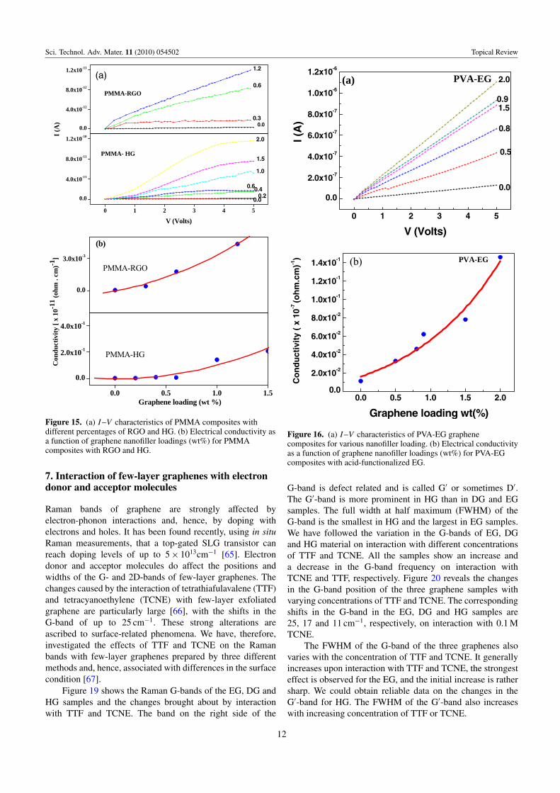
Figure 15(a) shows the typical I –V characteristicsof PMMA-graphene composites containing single-layergraphene (RGO) and HG (2–3 layers) as a filler material.The I –V curves are ohmic, with the current increasingwith the graphene content. The current is slightly higherfor PMMA-HG than PMMA-RGO composites. Figure 15(b)shows the variation of electrical conductivity in PMMA-RGOand HG composites. The conductivity increases withincreasing graphene content in both composites. Theconductivity value is two orders of magnitude higher forPMMA-RGO (10−14 �−1 cm−1) compared to PMMA-HG(10−12� −1 cm−1) composites, and PVA-EG shows higherconductivity than PMMA-EG and PMMA-HG composites.
Figure 16(a) shows the typical I –V characteristics ofPVA-EG composites containing varying weight percentagesof EG. Here, the I –V curves are more linear comparedto PMMA composites and the current increases with the
graphene content. The current is 104–105 times higher for thePVA-EG than PMMA-RGO and HG composites. Figure 14(b)plots the electrical conductivity of PVA-EG composites withvarying EG content. The conductivity increases with thegraphene content just as in the PMMA composites. Wehave not found a percolative transition with the increase ingraphene content in any studied composite.
We have also investigated the dielectric properties ofPMMA-RGO and PVA-EG composites. Figure 17(a) showsthe variation of dielectric function with frequency forPMMA-RGO composites with varying weight percentage ofRGO. The dielectric function decreases and then becomesconstant with increasing frequency. The variation of thedielectric function of PMMA-RGO composites at 1 MHz withthe graphene (RGO) content is shown in figure 17(b). Thedielectric function increases from 1 to 4 with increasing RGOcontent similarly to the electrical conductivity. Figure 18shows the variation of dielectric function with frequency forPVA-EG composites with different graphene contents. Heretoo, the dielectric function initially decreases and becomesconstant with increasing frequency. The inset in figure 18shows the variation of dielectric function at 1 MHz withEG content for PVA-EG composites. Here, the dielectricfunction increases with increasing EG content. Interestingly,the dielectric function values for PVA-EG are 10 times higherthan those for the PMMA-RGO composites.
Figure 15. (a) I –V characteristics of PMMA composites withdifferent percentages of RGO and HG. (b) Electrical conductivity asa function of graphene nanofiller loadings (wt%) for PMMAcomposites with RGO and HG.
7. Interaction of few-layer graphenes with electrondonor and acceptor molecules
Raman bands of graphene are strongly affected byelectron-phonon interactions and, hence, by doping withelectrons and holes. It has been found recently, using in situRaman measurements, that a top-gated SLG transistor canreach doping levels of up to 5 × 1013cm−1 [65]. Electrondonor and acceptor molecules do affect the positions andwidths of the G- and 2D-bands of few-layer graphenes. Thechanges caused by the interaction of tetrathiafulavalene (TTF)and tetracyanoethylene (TCNE) with few-layer exfoliatedgraphene are particularly large [66], with the shifts in theG-band of up to 25 cm−1. These strong alterations areascribed to surface-related phenomena. We have, therefore,investigated the effects of TTF and TCNE on the Ramanbands with few-layer graphenes prepared by three differentmethods and, hence, associated with differences in the surfacecondition [67].
Figure 19 shows the Raman G-bands of the EG, DG andHG samples and the changes brought about by interactionwith TTF and TCNE. The band on the right side of the
0 1 2 3 4 5
0.0
2.0x10⁻⁷
4.0x10⁻⁷
6.0x10⁻⁷
8.0x10⁻⁷
1.0x10⁻⁶
1.2x10⁻⁶
2.0
1.50.9
0.8
0.5
I (A
)
V (Volts)
0.0
PVA-EG(a)
0.0 0.5 1.0 1.5 2.00.0
2.0x10⁻²
4.0x10⁻²
6.0x10⁻²
8.0x10⁻²
1.0x10⁻¹
1.2x10⁻¹
1.4x10⁻¹
Co
nd
uct
ivit
y (
x 10
-7 (o
hm
.cm
)-1)
Graphene loading wt(%)
PVA-EG(b)
Figure 16. (a) I –V characteristics of PVA-EG graphenecomposites for various nanofiller loading. (b) Electrical conductivityas a function of graphene nanofiller loadings (wt%) for PVA-EGcomposites with acid-functionalized EG.
G-band is defect related and is called G′ or sometimes D′.The G′-band is more prominent in HG than in DG and EGsamples. The full width at half maximum (FWHM) of theG-band is the smallest in HG and the largest in EG samples.We have followed the variation in the G-bands of EG, DGand HG material on interaction with different concentrationsof TTF and TCNE. All the samples show an increase anda decrease in the G-band frequency on interaction withTCNE and TTF, respectively. Figure 20 reveals the changesin the G-band position of the three graphene samples withvarying concentrations of TTF and TCNE. The correspondingshifts in the G-band in the EG, DG and HG samples are25, 17 and 11 cm−1, respectively, on interaction with 0.1 MTCNE.
The FWHM of the G-band of the three graphenes alsovaries with the concentration of TTF and TCNE. It generallyincreases upon interaction with TTF and TCNE, the strongesteffect is observed for the EG, and the initial increase is rathersharp. We could obtain reliable data on the changes in theG′-band for HG. The FWHM of the G′-band also increaseswith increasing concentration of TTF or TCNE.
Figure 17. (a) Variation of dielectric function of PMMA-RGOcomposites with frequency for various nanofiller contents (wt%).(b) Dielectric function (at 1 MHz) as a function of graphene loading(wt%) for PMMA-RGO graphene composites.
0.0 0.2 0.4 0.6 0.8 1.0
1x101
2x101
3x101
2.01.5
0.8, 0.9
0.5
Die
lect
ric
cons
tant
Frequency (MHz)
PVA-EG
0.0
0 1 2
9
12
15
Die
lect
ric
cons
tant
@ 1
MH
z
Graphene loading (wt%)
PVA-EG
Figure 18. Variation of dielectric function with frequency forPVA-EG graphene composites having various nanofiller contents.The inset shows the dielectric function (at 1 MHz) as a function ofloading (wt%) for PVA composites with acid-functionalized EG.
Figure 21(a) shows the intensity ratio of the 2D- andG-bands, I(2D)/I(G), against the concentrations of TTF andTCNE. The 2D-band intensity decreases with the increase in
concentration of either TTF or TCNE, and the initial decreaseis sharp. The decrease in intensity is higher for EG and DGthan for HG. The intensity of the defect-related D-band alsovaries with the TTF/TCNE concentration, but in a manneropposite to that of the 2D-band, as shown in figure 21(b). Thisis because of the different origins of the 2D- and D-bands.The D-band, unlike the 2D-band, couples preferentially toelectronic states with the wave vector k such that 2q = k [68],where q is the scattering wave vector. Two scattering events,of which one is an elastic process involving defects and theother is inelastic involving a phonon, occur in the case of theD-band. In contrast, both processes are inelastic and involvephonons for the 2D-band. The I (D)/I (G) ratio increases moremarkedly for EG and DG than for HG samples, the initial risebeing sharp in all cases.
The variations in the Raman spectra and hence themagnitude of the charge-transfer interaction are the largest
for EG and the smallest for HG material. The changes inthe bandwidth, intensity and frequency caused by electrondonor and acceptor molecules occur sharply, with significantchanges at low concentrations. This is probably because of therelatively strong interaction induced by the donor and acceptormolecules of the very first layer compared to the next layers.This study shows the importance of the graphene surface indetermining doping effects through molecular charge transfer.
8. Conclusions
Graphenes with varying number of layers can be preparedusing several strategies, but definitive procedures are onlyavailable for single-layer graphene. Reduction of single-layergraphene oxide in solution allows easy manipulation andtransfer of graphene onto substrates. CVD results in singlelayers, but they are difficult to remove from the metal surface.Arc discharge of graphite in a hydrogen atmosphere yieldsgraphenes containing 2–3 layers and is suited for dopingwith boron or nitrogen. It must be noted that there is yet
no simple chemical method to produce graphene sampleswith the desired number of layers. The surface area ofgraphene depends on the number of layers and the methodof preparation, but is generally large (600–1600 m2 g−1).All graphenes seem to be ferromagnetic, independent ofthe preparation method. The electrical conductivity ofgraphene decreases with the increasing number of layersand this affects the electrical properties of polymer-graphenecomposites as well. The electrical conductivity of graphenecomposites formed with few-layer graphenes increases withincreasing graphene content, but shows no percolation,which is characteristic of single-layer graphene. Few-layergraphenes have relatively small thermopower as comparedwith single-layer graphene; they generally show n-typeconduction and field-effect transistors are readily fabricatedwith them. The best transistor characteristics are exhibitedby the graphene prepared by arc discharge of graphite inhydrogen. Few-layer graphenes with the largest surface areainteract more strongly with electron-donor and acceptormolecules through molecular charge transfer.
References
[1] Geim A K and Novoselov K S 2007 Nat. Mater. 6 183[2] Rao C N R, Sood A K, Subrahmanyam K S and Govindaraj A
2009 Angew. Chem. Int. Ed. 48 7752[3] Geim A K 2009 Science 324 1530[4] Rao C N R, Sood A K, Voggu R and Subrahmanyam K S 2010
J. Phys. Chem. Lett. 1 572[5] Allen M J, Tung V C and Kaner R B 2009 Chem. Rev. 110 132[6] Novoselov K S, Geim A K, Morozov S V, Jiang D, Katsnelson
M I, Grigorieva I V, Dubonos S V and Firsov A A 2005Nature 438 197
[7] Zhang Y, Tan J W, Stormer H L and Kim P 2005 Nature 438201
[8] Novoselov K S, Jiang Z, Zhang Y, Morozov S V, Stormer H L,Zeitler U, Maan J C, Boebinger G S, Kim P and Geim A K2007 Science 315 1379
[9] Lee C, Wei X, Kysar J W and Hone J 2008 Science 321 385[10] Dreyer D R, Park S, Bielawski C W and Ruoff R S 2010
Chem. Soc. Rev. 39 228[11] Novoselov K S, Geim A K, Morozov S V, Jiang D, Zhang Y,
Dubonos S V, Grigorieva I V and Firsov A A 2004 Science306 666
[12] Park S, An J, Jung I, Piner R D, An S J, Li X, Velamakanni Aand Ruoff R S 2009 Nano Lett. 9 1593
[13] Hummers W and Offeman R E 1958 J. Am. Chem. Soc.80 1339
[14] Choucair M, Thordarson P and Stride J A 2009 Nat. Nanotech.4 30
[15] Hernandez Y et al 2008 Nat. Nanotech. 3 563[16] Lotya M et al 2009 J. Am. Chem. Soc. 131 3611[17] Berger C et al 2004 J. Phys. Chem. B 108 19912[18] Rollings E, Gweon G-H, Zhou S Y, Mun B S, McChesney J L,
Hussain B S, Fedorov A V, First P N, de Heer W A andLanzara A 2006 J. Phys. Chem. Solids 67 2172
[19] Emtsev K V et al 2009 Nat. Mater. 8 203[20] Shelton J C, Patil H R and Blakely J M 1974 Surf. Sci. 43 493[21] Isett L C and Blakely J M 1976 Surf. Sci. 58 397[22] Eizenberg M and Blakely J M 1979 Surf. Sci. 82 228[23] Reina A, Jia X, Ho J, Nezich D, Son H, Bulovic V,
Dresselhaus M S and Kong J 2009 Nano Lett. 9 30[24] Schniepp H C, Li J-L, McAllister M J, Sai H, Herrera-Alonso
M, Adamson D H, Prud’homme R K, Car R, Saville D Aand Aksay I A 2006 J. Phys. Chem. B 110 8535
[25] Subrahmanyam K S, Vivekchand S R C, Govindaraj A andRao C N R 2008 J. Mater. Chem. 18 1517
[26] Staudenmaier L 1898 Ber. Dtsch. Chem. Ges. 31 1481[27] Stankovich S, Dikin D A, Piner R D, Kohlhaas K A,
Kleinhammes A, Jia Y, Wu Y, Nguyen S T and Ruoff R S2007 Carbon 45 1558
[28] Andersson O E, Prasad B L V, Sato H, Enoki T, Hishiyama Y,Kaburagi Y, Yoshikawa M and Bandow S 1998 Phys. Rev. B58 16387
[29] Prasad B L V, Sato H, Enoki T, Hishiyama Y, Kaburagi Y, RaoA M, Eklund P C, Oshida K and Endo M 2000 Phys. Rev. B62 11209
[30] Subrahmanyam K S, Panchakarla L S, Govindaraj A and RaoC N R 2009 J. Phys. Chem. C 113 4257
[31] Seshadri R, Govindaraj A, Aiyer H N, Sen R, Subbanna G N,Raju A R and Rao C N R 1994 Curr. Sci. 66 839
[32] Panchakarla L S, Subrahmanyam K S, Saha S K, GovindarajA, Krishnamurthy H R, Waghmare U V and Rao C N R2009 Adv. Mater. 21 4726
[33] Peigney A, Laurent Ch, Flahaut E, Bacsa R R and Rousset A2001 Carbon 39 507
[34] Ghosh A, Subrahmanyam K S, Krishna K S, Datta S,Govindaraj A, Pati S K and Rao C N R 2008 J. Phys. Chem.C 112 15704
[35] Nakada K, Fujita M, Dresselhaus G and Dresselhaus M S 1996Phys. Rev. B 54 17954
[36] Enoki T, Kawatsu N, Shibayama Y, Sato H, Kobori R,Maruyama S and Kaneko K 2001 Polyhedron 20 1311
[37] Wakabayashi K, Fujita M, Ajiki H and Sigrist M 1999 Phys.Rev. B 59 8271
[38] Enoki T and Kobayashi Y 2005 J. Mater. Chem. 15 3999[39] Enoki T and Takai K 2008 Dalton Trans. 3773[40] Enoki T, Kobayashi Y and Fukui K 2007 Int. Rev. Phys. Chem.
26 609[41] Castro E V, Peres N M R, Stauber T and Silva N A P 2008
Phys. Rev. Lett. 100 186803[42] Kusakabe K and Maruyama M 2003 Phys. Rev. B 67 092406[43] Lee H, Son Y W, Park N, Han S W and Yu J J 2005 Phys. Rev.
B 72 1745431[44] Bhowmick S and Shenoy V B 2008 J. Chem. Phys. 128 244717[45] Yazyev O V 2008 Phys. Rev. Lett. 101 037203
[46] Matte H S S R, Subrahmanyam K S and Rao C N R 2009J. Phys. Chem. C 113 9982
[47] Kopelvich Y, Dasilva R R, Torres J H S and Penicaud A 2003Phys. Rev. B 68 092408
[48] Dho J, Kim W S and Hur N H 2002 Phys. Rev. Lett. 89 027202[49] Shenoy V B and Rao C N R 2008 Phil. Trans. R. Soc. A 63 366[50] Ghosh M, Biswas K, Sundaresan A and Rao C N R 2006
J. Mater. Chem. 16 106[51] Dutta S, Lakshmi S and Pati S K 2008 Phys. Rev. B 77 073412[52] Morozov S V, Novoselov K S, Katsnelson M I, Schedin F,
Elias D C, Jaszczak J A and Geim A K 2008 Phys. Rev. Lett.100 016602
[53] Katsnelson M I and Geim A K 2008 Phil. Trans. R. Soc. 366195
[54] Ritter K A and Lyding J W 2008 Nanotechnology 19 015704[55] Son Y, Cohen M L and Louie S G 2006 Nature 444 347[56] Li X, Wang X, Zhang L, Lee S and Dai H 2008 Science 319
1229[57] Wang X, Ouyang Y, Li X, Wang H, Guo J and Dai H 2008
Phys. Rev. Lett. 100 206803[58] Meric I, Han M Y, Young A F, Ozyilmaz B, Kim P and
Shepard K L 2008 Nat. Nanotech. 3 654[59] Zuev Y M, Chang W and Kim P 2009 Phys. Rev. Lett. 102
096807[60] Late D J, Ghosh A, Subrahmanyam K S, Panchakarla L S,
Krupanidhi S B and Rao C N R 2010 Solid State Commun.150 734
[61] Prasad K E, Das B, Maitra U, Ramamurty U and Rao C N R2009 Proc. Natl Acad. Sci. USA 106 13186
[62] Ramanathan T et al 2008 Nat. Nanotech. 3 327[63] Das B, Prasad K E, Ramamurty U and Rao C N R 2009
Nanotechnology 20 125705[64] Stankovich S, Dikin D A, Dommett G H B, Kohlhaas K M,
Zimney E J and Stach E A 2006 Nature 442 282[65] Das A et al 2008 Nat. Nanotech. 3 210[66] Voggu R, Das B, Rout C S and Rao C N R 2008 J. Phys.:
Condens. Matter 20 472204[67] Subrahmanyam K S, Voggu R, Govindaraj A and Rao C N R
2009 Chem. Phys. Lett. 472 96[68] Saito R, Jorio A, Souza Filho A G, Dresselhaus G, Dresselhaus
M S and Pimenta M A 2002 Phys. Rev. Lett. 88 02740