IEEE/CSC & ESAS SUPERCONDUCTIVITY NEWS FORUM (global edition), July 2016. Page 1 of 5 A TES Bolometer for THz FT-Spectroscopy M. Kehrt, J. Beyer, C. Monte, J. Hollandt Physikalisch-Technische Bundesanstalt Abbestraße 2-12, Berlin, Germany E-Mail: [email protected]Abstract - We recently reported on a Transition Edge Sensor (TES) composite bolometer for Fourier Transform spectroscopy which was designed, built and characterized. The design is based on a superconducting thermistor with SQUID readout, SiN membrane technology and a thin film metal mesh absorber which is optimized for the spectral range from 0.1 THz to 3 THz. A noise equivalent power (NEP) of 3.8×10 -13 W/Hz 0.5 was achieved with a linear dynamic range of at least four orders of magnitude. Keywords (Index Terms) – Bolometer, absorber, TES, teraherz, spectrometer, Fourier transform Received: June 25, 2016; Accepted: July 12, 2016. Reference No. ST522; Category 4. I. INTRODUCTION AND BACKGROUND We recently reported on a Transition Edge Sensor (TES) composite bolometer for Fourier Transform spectroscopy which was designed, built and characterized [1]. Since 2009, the Physikalisch-Technische Bundesanstalt (PTB) provides calibration services for THz power as the only national metrology institute worldwide [2]. The knowledge of the optical properties of the used components is of major interest to achieve lowest uncertainties. These are obtained by the Fourier Transform (FT) spectroscopy using cooled detectors. The presented TES-bolometer is designed to replace conventional semiconductor-based bolometers in FT spectrometers operating in the frequency range from 0.1 THz to 3 THz. In the design, special emphasis was given to attaining a high and spectrally uniform absorption in this spectral range as well as on a highly linear response, in order to avoid artifacts in processing the FT spectroscopy data. The composite design allows a separate optimization of all relevant components, especially of the absorber and the thermistor. II. ABSORBER AND THERMISTOR DESIGN One approach realizing the desired spectrally flat absorption spectrum is matching the sheet resistance of the absorber to half the vacuum impedance. By using a continuous metal layer with a thickness smaller than the skin depth and a sheet resistance of R□ = 188 Ω, a theoretical maximum absorption of 0.5 can be obtained [3].
Transcript
IEEE/CSC & ESAS SUPERCONDUCTIVITY NEWS FORUM (global edition), July 2016.
Page 1 of 5
A TES Bolometer for THz FT-Spectroscopy M. Kehrt, J. Beyer, C. Monte, J. Hollandt
E-Mail: [email protected] Abstract - We recently reported on a Transition Edge Sensor (TES) composite bolometer for Fourier Transform spectroscopy which was designed, built and characterized. The design is based on a superconducting thermistor with SQUID readout, SiN membrane technology and a thin film metal mesh absorber which is optimized for the spectral range from 0.1 THz to 3 THz. A noise equivalent power (NEP) of 3.8×10⁻¹³ W/Hz0.5 was achieved with a linear dynamic range of at least four orders of magnitude.
Received: June 25, 2016; Accepted: July 12, 2016. Reference No. ST522; Category 4.
I. INTRODUCTION AND BACKGROUND We recently reported on a Transition Edge Sensor (TES) composite bolometer for Fourier Transform spectroscopy which was designed, built and characterized [1]. Since 2009, the Physikalisch-Technische Bundesanstalt (PTB) provides calibration services for THz power as the only national metrology institute worldwide [2]. The knowledge of the optical properties of the used components is of major interest to achieve lowest uncertainties. These are obtained by the Fourier Transform (FT) spectroscopy using cooled detectors. The presented TES-bolometer is designed to replace conventional semiconductor-based bolometers in FT spectrometers operating in the frequency range from 0.1 THz to 3 THz. In the design, special emphasis was given to attaining a high and spectrally uniform absorption in this spectral range as well as on a highly linear response, in order to avoid artifacts in processing the FT spectroscopy data. The composite design allows a separate optimization of all relevant components, especially of the absorber and the thermistor.
II. ABSORBER AND THERMISTOR DESIGN One approach realizing the desired spectrally flat absorption spectrum is matching the sheet resistance of the absorber to half the vacuum impedance. By using a continuous metal layer with a thickness smaller than the skin depth and a sheet resistance of R□ = 188 Ω, a theoretical maximum absorption of 0.5 can be obtained [3].
IEEE/CSC & ESAS SUPERCONDUCTIVITY NEWS FORUM (global edition), July 2016.
Page 2 of 5
A sufficiently thin continuous metal layer cannot be fabricated in high quality using materials accessible in standard thin film deposition. Therefore, the absorbers here are based on microstructured metal meshes to match the vacuum impedance.
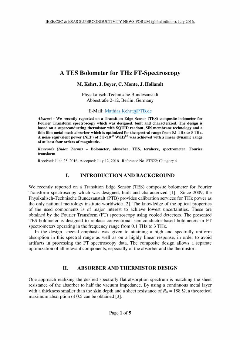
Fig. 1. Microscopic image of a microstructured metal mesh absorber. Here the design with square loops insight each mesh is shown.
In order to achieve a spectrally flat absorption the structural dimensions are much smaller than the relevant wavelengths. Two different designs were investigated systematically. One design consists of a simple mesh, the other design has additional square loops inside each mesh cell as shown in Fig. 1. Two structures, one of each design, were identified as optimum absorbers. Both structures have a strip width of 3 µm. The structure without loops in the grid has a pitch of 10 µm, the structure with loops a pitch of 35 µm. The absorbers were lithographically fabricated on 1 µm thin SiN membranes. The metal has a thickness of about 100 nm with a corresponding sheet resistance of approx. 20 Ω. The absorption α determined for both variants is spectrally flat and near its theoretical maximum of 0.5 for this approach, as illustrated in Fig. 2. The results were obtained by reflectance ρ and transmittance τ measurements by 𝛼 = 1 − 𝜌 − 𝜏. (1)
A further requirement of the bolometer is a high dynamic range in combination with a highly
Fig. 2. Spectrally flat absorption of the two selected absorber designs. Both designs are close to the theoretical absorption limit of 0.5.
IEEE/CSC & ESAS SUPERCONDUCTIVITY NEWS FORUM (global edition), July 2016.
Page 3 of 5
linear response. To achieve this, the thermistor is realized as a superconducting transition edge sensor (TES) which utilizes a steep resistive transition [4]. Our TESs are fabricated from bilayers of a superconducting (niobium) and a normal conducting (aluminium) metal with a thickness of approx. 20 nm for each layer. The critical temperature of the bilayer is reduced compared to a single layer of niobium. This ensures a superconducting operation of the leads (niobium) while the TES is in its transition range (Fig. 3.). The TES shows a superconducting transition at Tc ≈ 7.8 K with a width of approx. 20 mK. The achieved Tc is suitable for helium-cooled bolometers as intended here. Operating the TES in strong voltage biased condition a negative electrothermal feedback (nETF) extends the dynamic range [4] by ensuring that a constant sum of electrical heating power and incident radiative power stabilizes the TES at a fixed temperature inside the superconducting transition. The heating current, which is measured using an array of 16 Superconducting Quantum Interference Device (SQUID) current sensors, is directly related to the incident radiation.
Fig. 3. Resistive transition of the TES and, at higher temperature, of its leads.
Fig. 4. The TES-Bolometer, its mounting and its final setup. Left: Bolometer element with a TES in the centre, surrounded by the absorber mesh on a SiN membrane. Middle: Mounted bolometer with SQUID and wiring. Right: Assembly of filter wheel, Winston Cone, bolometer mount and radiation shield.
IEEE/CSC & ESAS SUPERCONDUCTIVITY NEWS FORUM (global edition), July 2016.
Page 4 of 5
More thermal design details can be found in [1]. Several composite bolometers consisting of TES thermistors and both types of absorber structures were fabricated in a multilayer lithographic process on SiN membranes. On the left of Fig. 4 a bolometer element with a TES in the center is shown. The thermistor in the center is surrounded by the absorber with a physical dimension of 3.3 mm in square. The mounted bolometer with the SQUID readout and wiring is shown in the middle of Fig. 4.
III. CHARACTERIZATION The complete detector was built up in a liquid helium cooled cryostat. The bolometer is shielded from the warmer surrounding inside of the cryostat by a gold plated housing. To reduce reflected FIR radiation the inner side of the housing is coated by grained SiC. The THz radiation to be detected passes a wedged diamond window and one of several cooled filters in a filter wheel and is concentrated by a Winston cone onto the bolometer (Fig. 4, right). For the electrical characterization the bolometer was operated in this environment without a radiant load by replacing one of the filters by a copper plate. The dark signal was recorded by a spectrum analyzer. The measured noise spectral density divided by the responsivity [5] leads to a noise equivalent power (NEP) of 3.8×10⁻¹³ W/Hz0.5 for typical operating conditions. Additionally, the linear response range was determined with tunable THz radiation at the Metrology Light Source (MLS), the electron storage ring of PTB [6]. To investigate a power range over several orders of magnitude two operation modes of the MLS were used: normal operating mode providing incoherent THz radiation as well as low-α mode providing coherent THz radiation up to the mW range. In normal mode of operation four different ring currents were used. In low-α mode the MLS was operated at one ring current. For a finer attenuation of the radiant power two wire grid polarizers at different angle settings were utilized. In low-α mode the bolometer was compared with a calibrated broadband THz detector [7]. Here the bolometer shows a linear response up to 330 µW as shown in Fig. 5 in lightblue squares. In normal mode of operation the calibrated detector was not sensitive enough for a comparison. But here the radiant power is known to be strictly proportional to the ring current and the TES bolometer shows a linear response according to the calculated attenuation due to the angle settings of the polarizers. To determine the missing proportionality factor the results of the highest ring current of 140 mA were extrapolated and scaled to the results obtained in low-α mode. The compiled consistent results of all measurements at both operating modes of the MLS are shown in Fig. 5. The TES bolometer provides a linear response over a range of at least four orders of magnitude.
IEEE/CSC & ESAS SUPERCONDUCTIVITY NEWS FORUM (global edition), July 2016.
Page 5 of 5
Fig. 5. The linear response range of the TES bolometer was determined to be four orders of magnitude by measurements at an electron storage ring (Metrology Light Source of PTB). Two modes of operation of the storage ring (normal mode and THz coherent synchrotron radiation CSR) with different ring currents were used to systematically vary the radiant power on the bolometer.
REFERENCES [1] M. Kehrt, C. Monte, J. Beyer, and J. Hollandt, “A highly linear superconducting bolometer for quantitative THz Fourier transform spectroscopy“, Opt. Express, 23, 11170-11182, (2015). [2] A. Steiger,M. Kehrt; C. Monte, R. Müller, “Traceable terahertz power measurement from 1 THz to 5 THz“, Opt. Express, 21, 14466-14473, (2013). [3] W. Woltersdorff, “Über die optischen Konstanten dünner Metallschichten im langwelligen Ultrarot“, Z. Phys., 91, 230–252, (1934). [4] P. L. Richards, ”Bolometers for infrared and millimeter waves”, Appl. Phys., 76, 1–24, (1994). [5] K. Irwin and G. Hilton. “Transition-edge sensors”. In C. Enss, editor, Cryogenic Particle Detection, vol. 99 of “Topics. Appl. Phys”., pp. 63–150. Springer, Berlin, Heidelberg, (2005). [6] J. Feikes, M. von Hartrott, M. Ries, et al., “Metrology Light Source: The first electron storage ring optimized for generating coherent THz radiation,” Phys. Rev. ST Accel. Beams, 14, 030705, (2011). [7] R. Müller, W. Bohmeyer, M. Kehrt, K. Lange, C. Monte, and A. Steiger, “Novel detectors for traceable THz power measurements,” J. Infrared Millim. Terahertz Waves, 35, 659-670, (2014).