A Top-Down Verilog-A Design on the Digital Phase-Locked Loop Report of the Project Assignment Presented for Ph.D Qualifying Exam By Ching-Hong Wang Advisory Committee: Steven Bibyk, Professor of the ECE Department, Advisor Bradley D. Clymer, Professor of the ECE Department Eylem Ekici, Professor of the ECE Department
Transcript
A Top-Down Verilog-A Design on the Digital Phase-Locked Loop
Report of the Project Assignment
Presented for Ph.D Qualifying Exam
By
Ching-Hong Wang
Advisory Committee:
Steven Bibyk, Professor of the ECE Department, Advisor
Bradley D. Clymer, Professor of the ECE Department
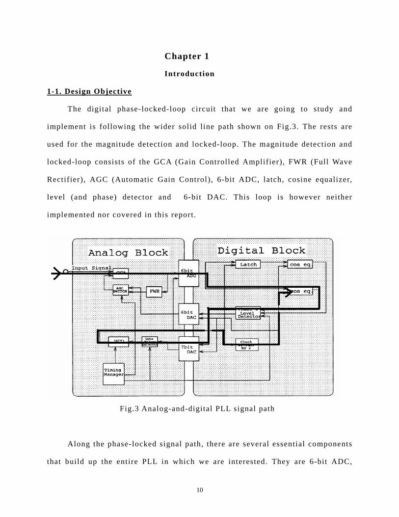
clock divider. It is very similar to a conventional phase-locked loop but replace
the charge pump block with a combination of the digital counter and 7-bit DAC.
The counter is embedded into the digital phase detector and works as the input
level for the 7-bit DAC. As the output of phase detector sends a plus or minus
signal to the counter, it will count up or down and represents the digitized level
of an input for DAC. Following sections will basically introduce the traditional
phase-locked loop circuit blocks.
Within the digital block there is a cosine equalizer that behaves as a digital
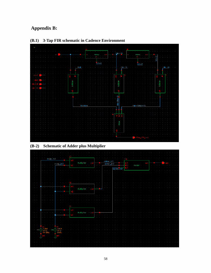
fi lter and is also called as a 3-Tap finite impulse response (3-Tap FIR) filter. The
cosine equalizer, digital phase detector and 7-bit DAC compose the function
same as that of the conventional phase frequency detector plus charge pump. We
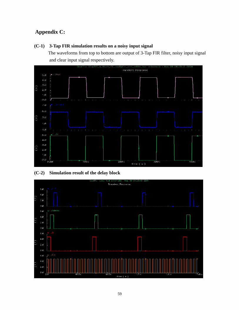
can refer to the simulation result on Appendix C-1 that shows the 3-Tap FIR filter
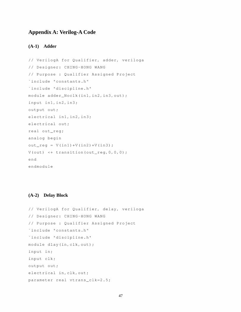
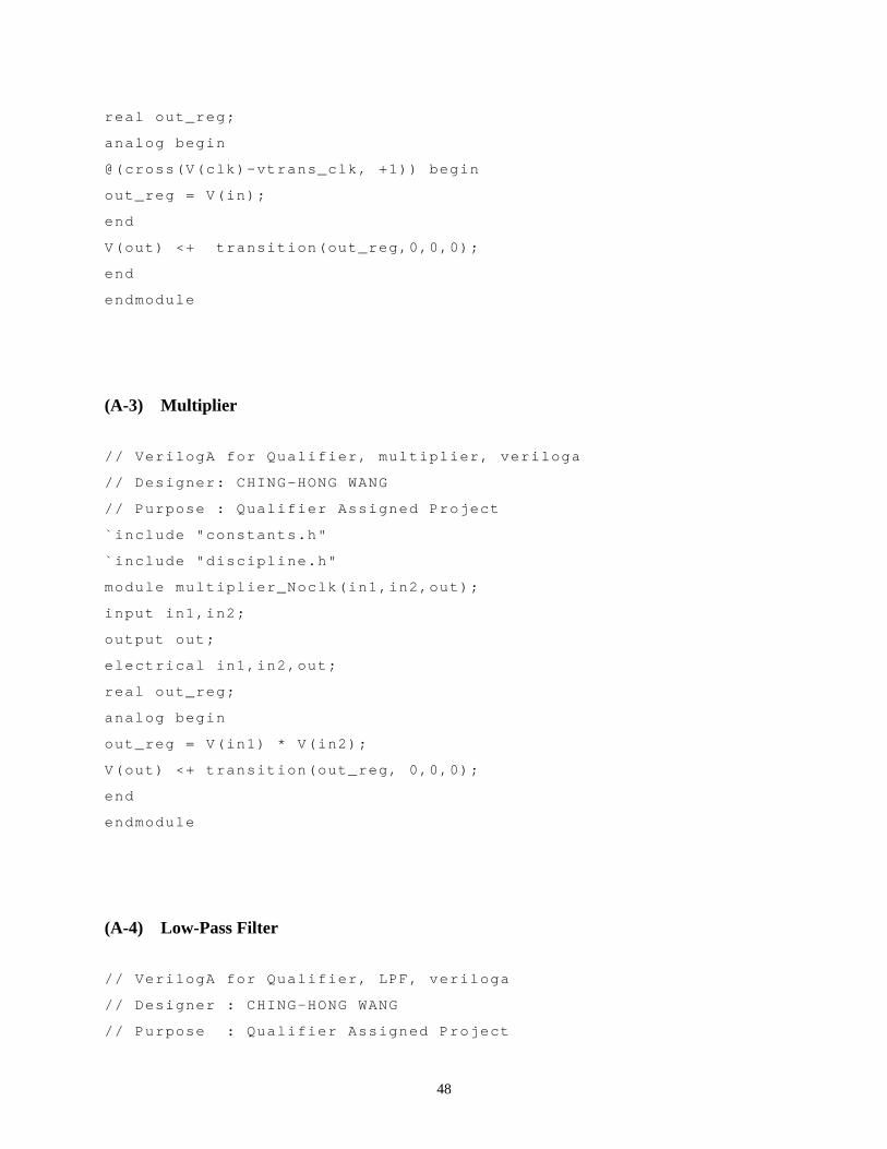
function on a noisy input signal. The 3-Tap FIR filter consists of one adder, two
delay blocks and three multipliers. Appendix A-1 is the Verilog-A code for the
adder. The delay block is modeled as the Appendix A-2 and its simulation result
is on Appendix C-2. The Verilog-A model for the multiplier is on Appendix A-3.
11
1-2. Conventional Phase-Locked loop
Depends on the different purposes, the phase-locked loop (PLL) most often
deals with signals or clocks to reduce timing jitters, suppresses clock skews,
synthesizes higher frequencies, and assists data and clock recoveries.
Traditionally there are four kinds of phase-locked loops. They are linear PLL
(LPLL), digital PLL (DPLL), all-digital PLL (ADPLL), and software PLL (SPLL)
all around the world. However, the phase-locked-loop circuit is conventionally
based on three essential components.[3]
1. Voltage-Controlled-Oscillator (VCO)
2. Loop Filter (LF)
3. Phase Detector (PD)
The phase detector first compares the differences between the input signal
and the VCO output signal. It then generates a phase error according to the
difference. Passing through the loop filter, the feedback loop will present a
control signal for the voltage-controlled oscillator to either increase or decrease
the oscillating frequency in accordance to the controlled voltage level.
Recursively, the entire phase-locked loop will be able to lock the input signal
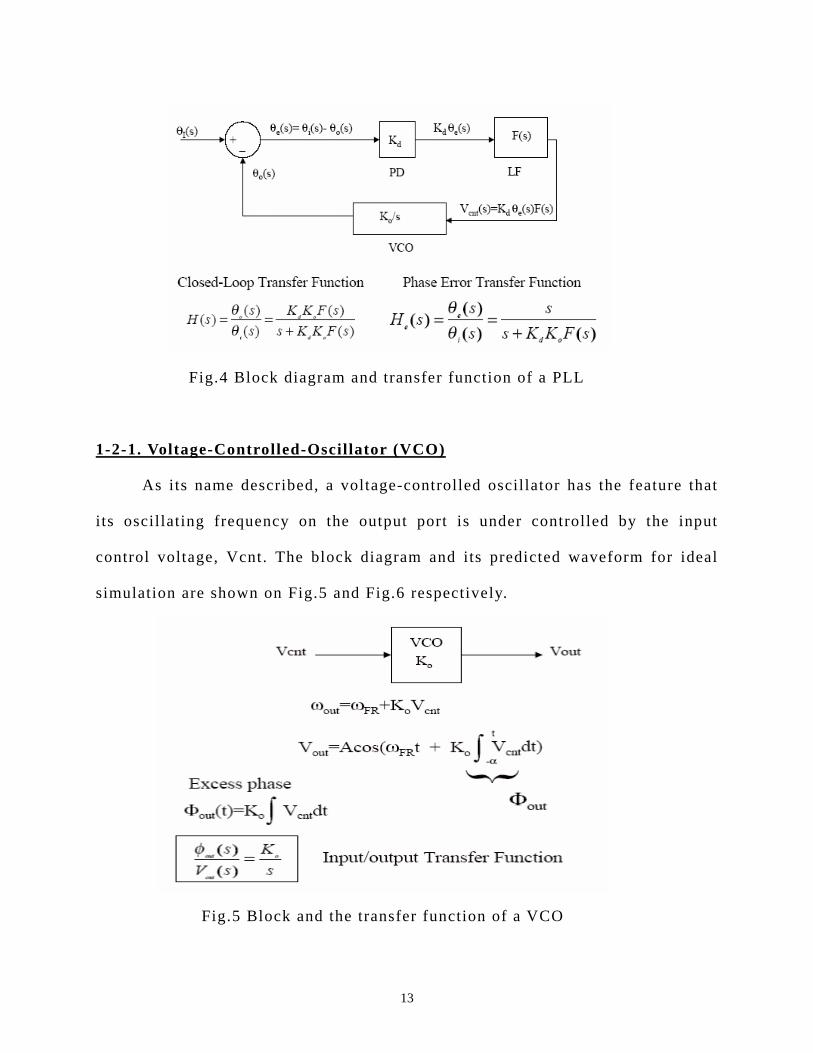
within a lock-in time. Fig.4 shows the conventional phase-locked-loop block
diagrams as well as its transfer functions.
12
Fig.4 Block diagram and transfer function of a PLL
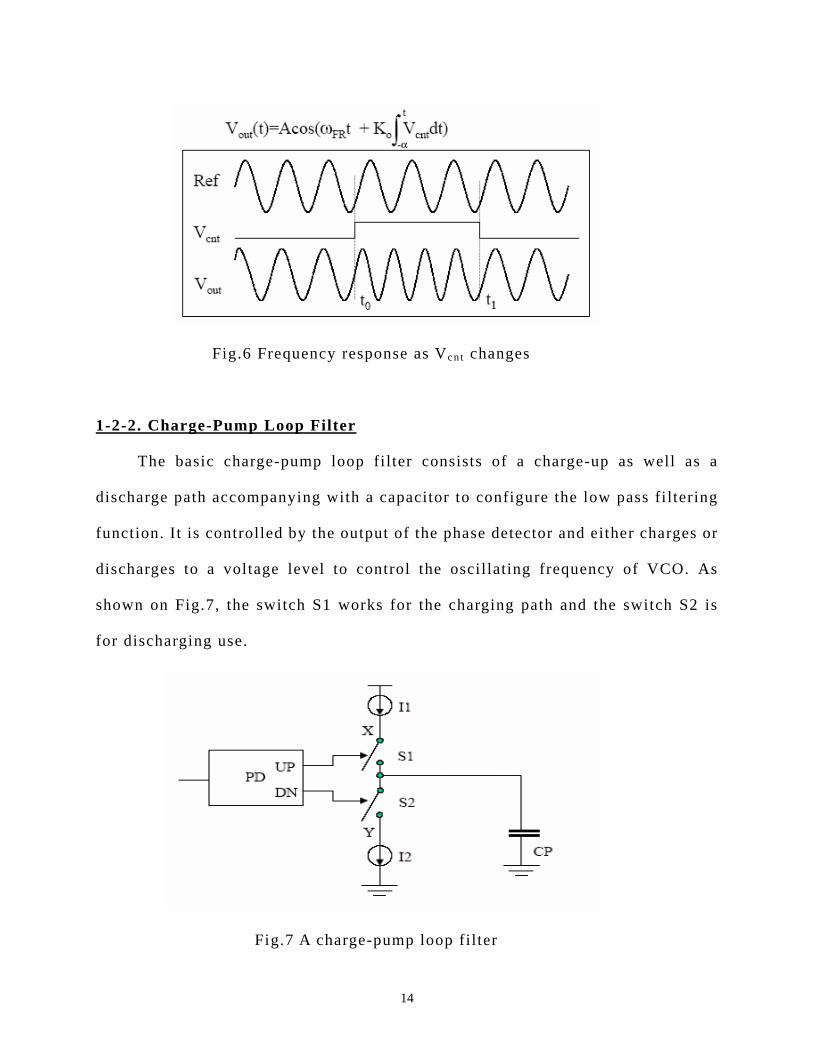
1-2-1. Voltage-Controlled-Oscillator (VCO)
As its name described, a voltage-controlled oscillator has the feature that
its oscillating frequency on the output port is under controlled by the input
control voltage, Vcnt. The block diagram and its predicted waveform for ideal
simulation are shown on Fig.5 and Fig.6 respectively.
Fig.5 Block and the transfer function of a VCO
13
Fig.6 Frequency response as Vc n t changes
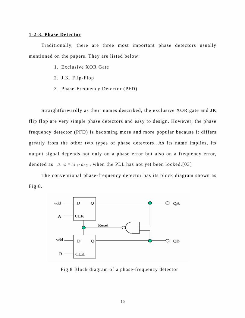
1-2-2. Charge-Pump Loop Filter
The basic charge-pump loop filter consists of a charge-up as well as a
discharge path accompanying with a capacitor to configure the low pass filtering
function. It is controlled by the output of the phase detector and either charges or
discharges to a voltage level to control the oscillating frequency of VCO. As
shown on Fig.7, the switch S1 works for the charging path and the switch S2 is
for discharging use.
Fig.7 A charge-pump loop filter
14
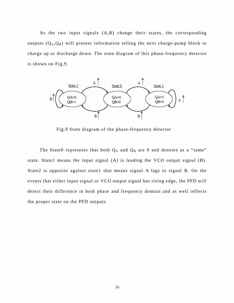
1-2-3. Phase Detector
Traditionally, there are three most important phase detectors usually
mentioned on the papers. They are listed below:
1. Exclusive XOR Gate
2. J.K. Flip-Flop
3. Phase-Frequency Detector (PFD)
Straightforwardly as their names described, the exclusive XOR gate and JK
flip flop are very simple phase detectors and easy to design. However, the phase
frequency detector (PFD) is becoming more and more popular because it differs
greatly from the other two types of phase detectors. As its name implies, its
output signal depends not only on a phase error but also on a frequency error,
denoted as Δ ω =ω 1-ω 2 , when the PLL has not yet been locked.[03]
The conventional phase-frequency detector has its block diagram shown as
Fig.8.
Fig.8 Block diagram of a phase-frequency detector
15
As the two input signals (A,B) change their states, the corresponding
outputs (QA,QB) will present information telling the next charge-pump block to
charge up or discharge down. The state diagram of this phase-frequency detector
is shown on Fig.9.
Fig.9 State diagram of the phase-frequency detector
The State0 represents that both QA and QB are 0 and denotes as a “same”
state. State1 means the input signal (A) is leading the VCO output signal (B).
State2 is opposite against state1 that means signal A lags to signal B. On the
events that either input signal or VCO output signal has rising edge, the PFD will
detect their difference in both phase and frequency domain and as well reflects
the proper state on the PFD outputs
16
Chapter 2
Matlab System-Level Design and Simulation
As mentioned previously, the modern complicated analog and mixed signal
chip designs require system level design and simulation prior to getting into
detail circuit designs. This process can assist designers evaluating their design
architectures before really struggling on some unsatisfying specifications.
Matlab, a well known powerful numerical simulation tool, is one of the
good choices to do system level design and simulation. There are two approaches
to implement the system level tasks. First, designers can use the embedded M-file
functions or model their preferred M-files to do the system simulation. The
second approach is the use of simulink, an embedded block diagram method of
Matlab, to accomplish those system level design and simulation. Although
Matlab is a nice simulation tool for our system level design, the emphasis is not
on it in this report. The reason that Matlab is not a major design technique
instead in this report is its poor compatibility with pure hardware description
languages. We will only go through the matlab design methodologies as section
2-1 and section 2-2.
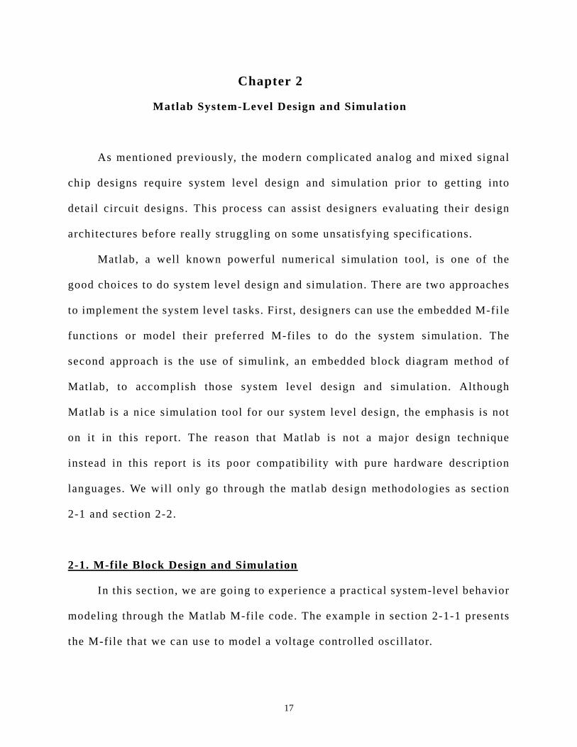
2-1. M-file Block Design and Simulation
In this section, we are going to experience a practical system-level behavior
modeling through the Matlab M-file code. The example in section 2-1-1 presents
the M-file that we can use to model a voltage controlled oscillator.
17
2-1-1. Voltage-Controlled-Oscillator
The M-file described on Fig.10 is a simple example to simulate a
voltage-controlled oscillator. It comes out the simulation result on Fig.11. Here
we use an embedded Matlab function, vco(), to model our required signal. Such
vco.m file is located under the signal processing toolbox. Fig.12 presents us in
details what the embedded function vco() should be.
% Matlab M-file, VCO Design % Designer: CHING-HONG WANG Fs = 100; t = 0:1/Fs:2; x = sin(2*pi*t); y = vco(x,10,Fs); subplot(2,1,1),plot(t,x,':') title('Control Signal') xlabel('Time (sec)'), ylabel('Voltage (V)') subplot(2,1,2),plot(t,y) title('VCO Output Response') xlabel('Time (sec)'), ylabel('Voltage (V)')
Fig.10 M-file for a voltage-controlled oscillator
Fig.11 Simulation results of a VCO designed in M-file
18
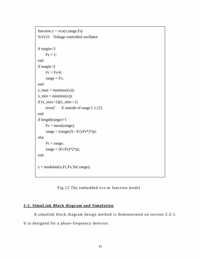
Fig.12 The embedded vco.m function model
function y = vco(x,range,Fs) %VCO Voltage controlled oscillator
nargin<3 if Fs = 1;
/4;
x(x));
range [-1,1]')
odulate(x,Fc,Fs,'fm',range);
end gin<2 if nar
Fc = Fs range = Fc;end
ax = max(max_mx_min = min(min(x)); if (x_max>1)|(x_min<-1) error(' X outside of end if length(range)>1 Fc = mean(range); range = (range(2) - Fc)/Fs*2*pi; else
c = range; F range = (Fc/Fs)*2*pi; end y = m
2-2. S muLink Block diagram and Simulationi
demonstrated on section 2-2-1.
It is d
A simulink block diagram design method is
esigned for a phase-frequency detector.
19
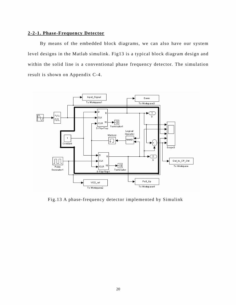
2-2-1. Phase-Frequency Detector
lock diagrams, we can also have our system
level
By means of the embedded b
designs in the Matlab simulink. Fig13 is a typical block diagram design and
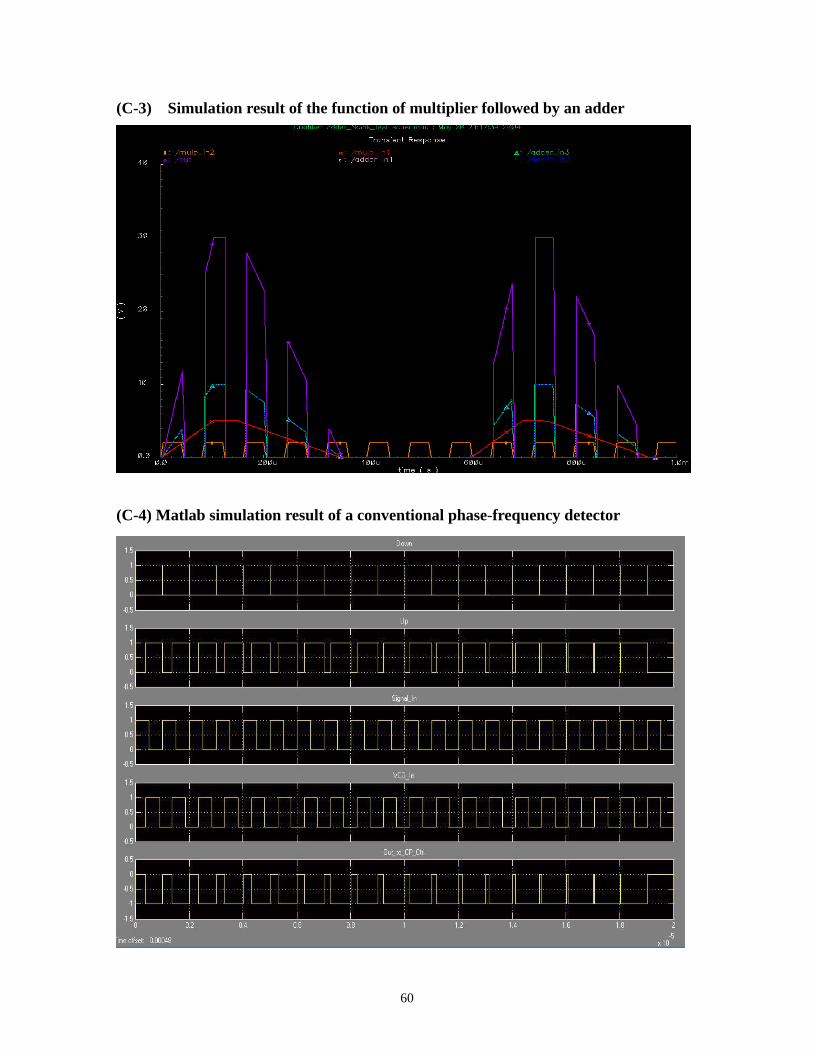
within the solid line is a conventional phase frequency detector. The simulation
result is shown on Appendix C-4.
Fig.13 A phase-frequency detector implemented by Simulink
20
Chapter 3
Verilog-A System and Simulation
erilog-A, an advanced analog and mixed signal hardware description
langu
3-1. VCO Design in Verilog-A
-Level Design
V
age that we emphasized at the beginning, plays the most important role for
our digital phase-locked loop design in this report. The compatibility with pure
HDLs as well as its system simulation ability catches our whole attentions. In
this chapter, there are two design examples demonstrating its functions. Section
3-1 is an example of designing the voltage controlled oscillator in Verilog-A. The
practical design of a phase-frequency detector in the digital block presented on
the paper [2] is studied and implemented in Verilog-A as well in section 3-2. All
the other portions not included in this chapter are covered inside the appendices.
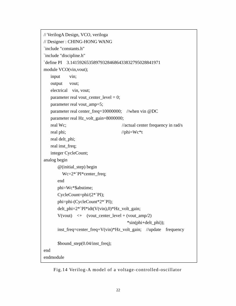
trate a voltage controlled oscillator modeled by
the V
In this section, we demons
erilog-A HDL. The detail code is shown on Fig.14. A central frequency is
predefined as 10MHz when no control voltage applies. The phase of its
sinusoidal output signal is varying and decided by the controlled voltage level.
As the control voltage level increases, the frequency of its output signal also
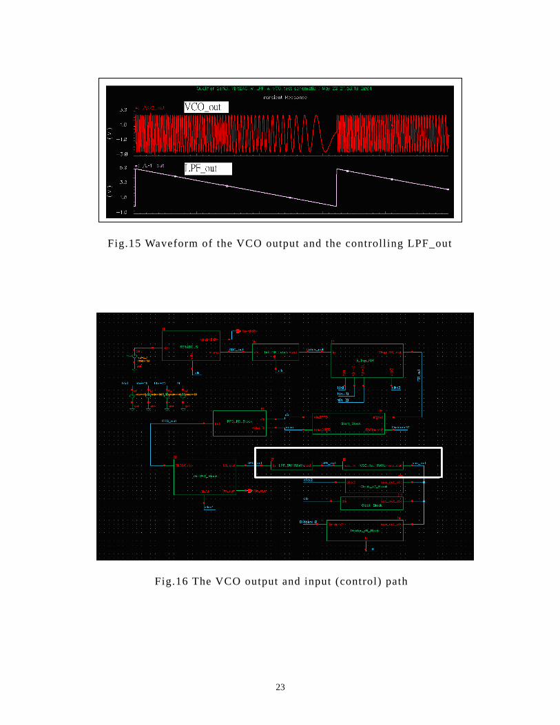
increases proportionally. Refering to Fig.15, it presents to us that a higher
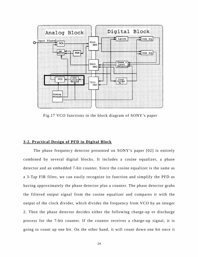
voltage level of LPF_out produces a higher oscillating frequency, VCO_out. This
is corresponding to the solid rectangular region selected on Fig.16 and Fig.17.
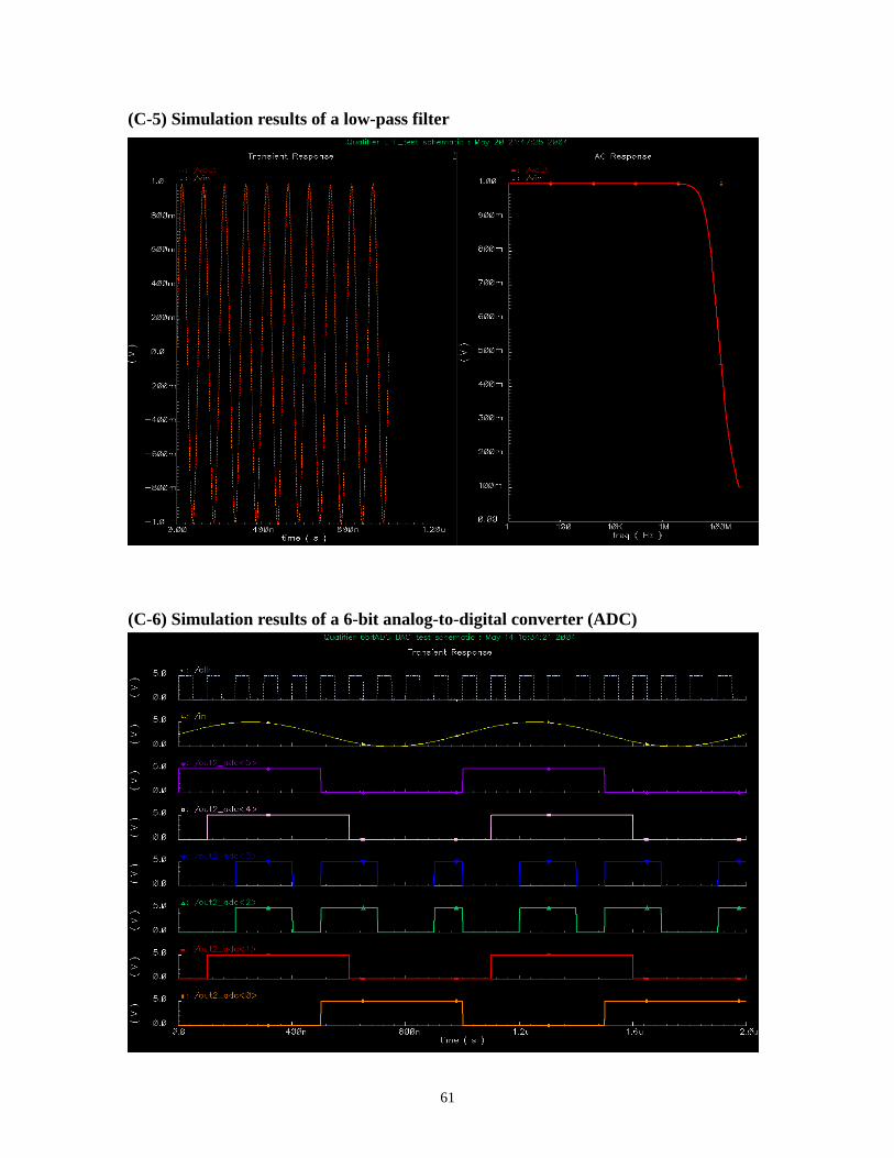
Appendix A-4 shows the Verilog-A code for a low-pass filter (LPF). The
simulation result of a LPF is on Appendix C-5.
21
Fig.14 Verilog-A model of a voltage-controlled-oscillator
// VerilogA Design, VCO, veriloga // Designer : CHING-HONG WANG `include "constants.h" `include "discipline.h" `define PI 3.141592653589793284686433832795028841971 module VCO(vin,vout); input vin; output vout; electrical vin, vout; parameter real vout_center_level = 0; parameter real vout_amp=5; parameter real center_freq=10000000; //when vin @DC
in rad/s
eq;
p/2) phi));
parameter real Hz_volt_gain=8000000; r ctual center frequencyeal Wc; //a real phi; //phi=Wc*t real delt_phi; real inst_freq; integer CycleCount; analog begin
begin @(initial_step) Wc=2*`PI*center_fr
end phi=Wc*$abstime; CycleCount=phi/(2*`PI); phi=phi-(CycleCount*2*`PI); delt_phi=2*`PI*idt(V(vin),0)*Hz_volt_gain; V(vout) <+ (vout_center_level + (vout_am *sin(phi+delt_ inst_freq=center_freq+V(vin)*Hz_volt_gain; //update frequency $bound_step(0.04/inst_freq); end
odule endm
22
Fig.15 Waveform of the VCO output and the controlling LPF_out
Fig.16 The VCO output and input (control) path
23
Fig.17 VCO functions in the block diagram of SONY’s paper
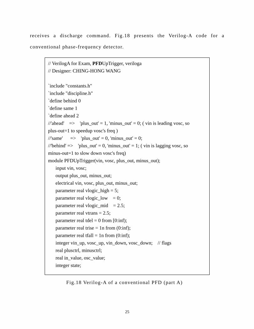
3-2. Practical Design of PFD in Digital Block
SONY’s paper [02] is entirely
comb
The phase frequency detector presented on
ined by several digital blocks. It includes a cosine equalizer, a phase
detector and an embedded 7-bit counter. Since the cosine equalizer is the same as
a 3-Tap FIR filter, we can easily recognize its function and simplify the PFD as
having approximately the phase detector plus a counter. The phase detector grabs
the fil tered output signal from the cosine equalizer and compares it with the
output of the clock divider, which divides the frequency from VCO by an integer
2. Then the phase detector decides either the following charge-up or discharge
process for the 7-bit counter. If the counter receives a charge-up signal, i t is
going to count up one bit . On the other hand, it will count down one bit once it
24
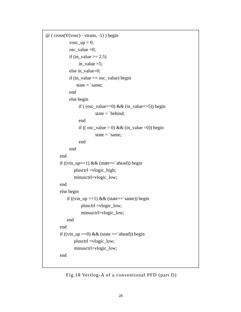
receives a discharge command. Fig.18 presents the Verilog-A code for a
conventional phase-frequency detector.
Fig.18 Verilog-A of a conventional PFD (part A)
// VerilogA for Exam, PFDUpTrigger, veriloga
plus_out' = 1, 'minus_out' = 0; ( vin is leading vosc, so
minus_out;
;
flags
// Designer: CHING-HONG WANG `include "constants.h" `include "discipline.h" `define behind 0 `define same 1 `define ahead 2 //'ahead' => 'plus-out=1 to speedup vosc's freq ) //'same' => 'plus_out' = 0, 'minus_out' = 0; //'behind' => 'plus_out' = 0, 'minus_out' = 1; ( vin is lagging vosc, so minus-out=1 to slow down vosc's freq) module PFDUpTrigger(vin, vosc, plus_out, minus_out); input vin, vosc;
minus_out; output plus_out, electrical vin, vosc, plus_out, parameter real vlogic_high = 5; parameter real vlogic_low = 0; parameter real vlogic_mid = 2.5; parameter real vtrans = 2.5;
0:inf); parameter real tdel = 0 from [ parameter real trise = 1n from (0:inf) parameter real tfall = 1n from (0:inf); integer vin_up, vosc_up, vin_down, vosc_down; // real plusctrl, minusctrl; real in_value, osc_value; integer state;
25
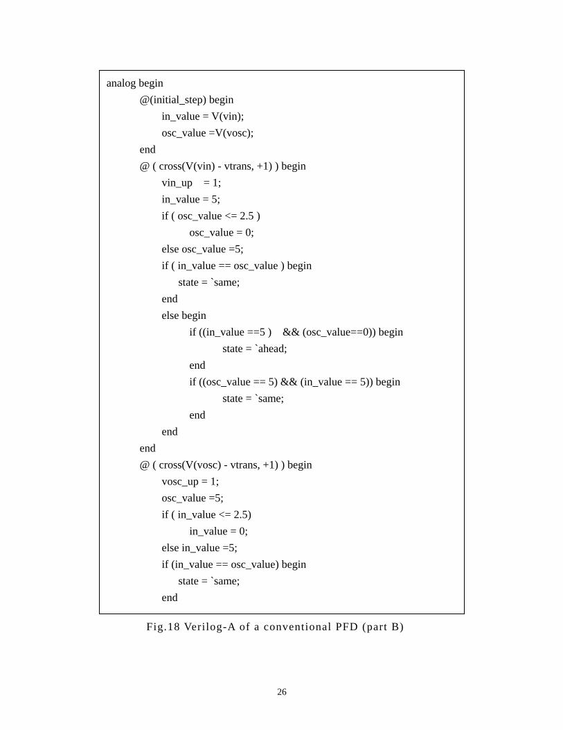
analog begin begin
2.5 )
) begin
value ==5 ) && (osc_value==0)) begin
(in_value == 5)) begin
- vtrans, +1) ) begin
2.5)
begin
@(initial_step) in_value = V(vin); osc_value =V(vosc); end @ ( cross(V(vin) - vtrans, +1) ) begin vin_up = 1; in_value = 5; if ( osc_value <= osc_value = 0; else osc_value =5; if ( in_value == osc_value state = `same;
end e gin lse be if ((in_ state = `ahead; end
== 5) && if ((osc_value state = `same; end end end @ ( cross(V(vosc) vosc_up = 1; osc_value =5; if ( in_value <= in_value = 0; else in_value =5; if (in_value == osc_value) state = `same; end
erilog-A of a conventional PFD (part B) Fig.18 V
26
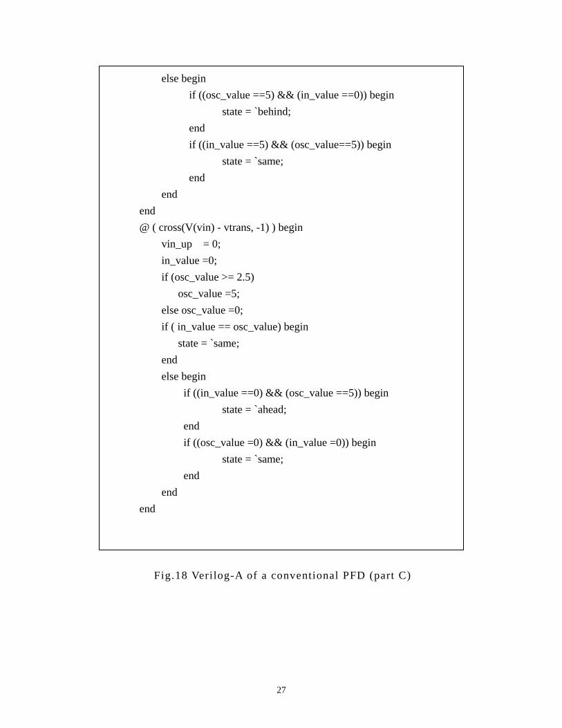
Fig.18 Verilog-A of a conventional PFD (part C)
else begin if ==5) && (in_value ==0)) begin
sc_value==5)) begin
- vtrans, -1) ) begin
begin
_value ==0) && (osc_value ==5)) begin
lue =0)) begin
((osc_value state = `behind; end
_value ==5) && (o if ((in state = `same; end end end @ ( cross(V(vin) vin_up = 0; in_value =0; if (osc_value >= 2.5) osc_value =5; else osc_value =0; if ( in_value == osc_value) state = `same; end
else begin if ((in state = `ahead; end
sc_value =0) && (in_va if ((o state = `same; end end end
27
Fig.18 Verilog-A of a conventional PFD (part D)
@ ( cross(V(vosc) - vtrans, -1) ) begin
begin
&& (in_value==5)) begin
=0)) begin
te==`ahead)) begin
==1) && (state==`same)) begin
==0) && (state ==`ahead)) begin
vosc_up = 0; osc_value =0; if (in_value >= 2.5) in_value =5; else in_value=0; if (in_value == osc_value) state = `same; end
gin else be if ( (osc_value==0) state = `behind; end
= 0) && (in_value if (( osc_value state = `same; end end end
if ((vin_up==1) && (sta plusctrl =vlogic_high; minusctrl=vlogic_low; end
egin else b if ((vin_up plusctrl =vlogic_low;
minusctrl=vlogic_low; end end if ((vin_up plusctrl =vlogic_low;
minusctrl=vlogic_low; end
28
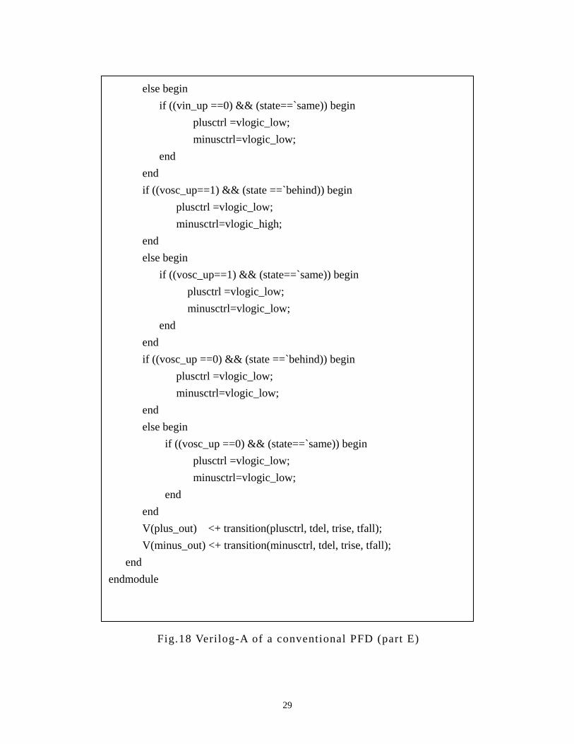
Fig.18 Verilog-A of a conventional PFD (part E)
else begin if ==0) && (state==`same)) begin
te ==`behind)) begin
_up==1) && (state==`same)) begin
==0) && (state ==`behind)) begin
==0) && (state==`same)) begin
transition(plusctrl, tdel, trise, tfall);
((vin_up plusctrl =vlogic_low;
minusctrl=vlogic_low; end end
if ((vosc_up==1) && (sta plusctrl =vlogic_low;
; minusctrl=vlogic_high end
egin else b if ((vosc plusctrl =vlogic_low;
minusctrl=vlogic_low; end end if ((vosc_up plusctrl =vlogic_low;
minusctrl=vlogic_low; end else begin if ((vosc_up plusctrl =vlogic_low;
minusctrl=vlogic_low; end end V(plus_out) <+ V(minus_out) <+ transition(minusctrl, tdel, trise, tfall); end
endmodule
29
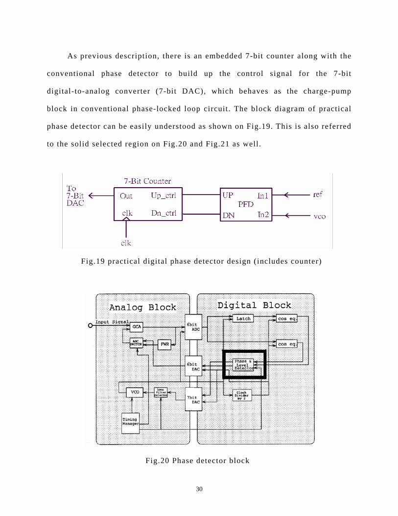
As previous description, there is an embedded 7-bit counter along with the
conventional phase detector to build up the control signal for the 7-bit
digital-to-analog converter (7-bit DAC), which behaves as the charge-pump
block in conventional phase-locked loop circuit . The block diagram of practical
phase detector can be easily understood as shown on Fig.19. This is also referred
to the solid selected region on Fig.20 and Fig.21 as well.
Fig.19 practical digital phase detector design (includes counter)
Fig.20 Phase detector block
30
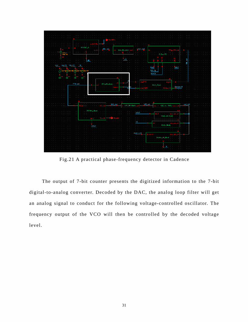
Fig.21 A practical phase-frequency detector in Cadence
he output of 7-bit counter presents the digitized information to the 7-bit
digita
T
l-to-analog converter. Decoded by the DAC, the analog loop filter will get
an analog signal to conduct for the following voltage-controlled oscillator. The
frequency output of the VCO will then be controlled by the decoded voltage
level.
31
Chapter 4
Tes s
In addition to the desi ned function blocks, it is also important to have test
bench
following
distri
aussian)
T function generators used in this report are focused on the
pseud
4-1. Random-Bit Noise Ge erator
t Bench Studie
g
es that can help verify the performances of our designs. Verilog-A provides
several commands to generate random numbers in specified distributions that
may be useful for our needs. The test benches studied in this report only provide
a starting point to experience verification processes. To generate more sets of test
benches in the future can assist and modify our design more perfectly.
Verilog-A provides functions to generate random numbers in the
bution patterns:
* Pseudo-Random
* Uniform
* Normal (G
* Exponential
* Poisson
he main
o-random, uniform and normal distributions. They are described in the
following sections.
n
vironments that a real circuit may encounter,
i t is
To realistically simulate the en
necessary to include noise generators for our simulations. The
uniform-distributed, normal-distributed (Gaussian) and pseudo-random noise
32
generators are discussed.
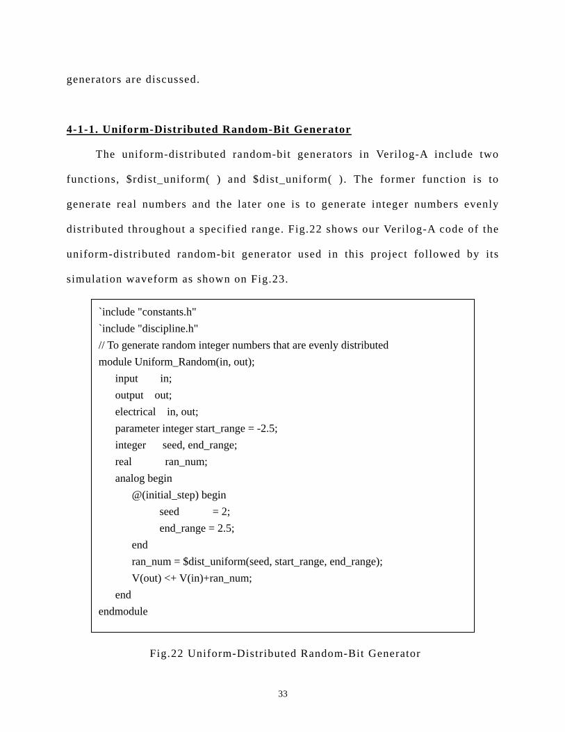
4-1-1. Uniform-Distributed Random-Bit Generator
in Verilog-A include two
funct
ig.22 Uniform-Distributed Random-Bit Generator
The uniform-distributed random-bit generators
ions, $rdist_uniform( ) and $dist_uniform( ). The former function is to
generate real numbers and the later one is to generate integer numbers evenly
distributed throughout a specified range. Fig.22 shows our Verilog-A code of the
uniform-distributed random-bit generator used in this project followed by its
simulation waveform as shown on Fig.23.
`include "constants.h" `include "discipline.h" // To generate random integer numbers that are evenly distributed
out; = -2.5;
(seed, start_range, end_range);
module Uniform_Random(in, out); input in; output out; electrical in, parameter integer start_range integer seed, end_range; real ran_num; analog begin
begin @(initial_step) seed = 2; end_range = 2.5; end
= $dist_uniform ran_num V(out) <+ V(in)+ran_num; end
endmodule
F
33
Fig.23 Waveform of the Uniform-Distributed Random-Bit Generator
-1-2. Normal-Distributed Random-Bit Generator
4
enerator in Verilog-A code
is sho
Fig.24 Normal-Distributed Random-Bit Generator
The normal-distributed (Gaussian) random-bit g
wn on Fig.24. Its simulation waveform can be apparently seen on Fig.25.
integer seed; parameter integer mean=0;
al(seed,mean,standard_deviation);
parameter integer standard_deviation=1; real ran_num; analog begin
ep) begin @(initial_st seed = 25; end
= $rdist_norm ran_num V(out) <+ V(in)+ran_num; end
34
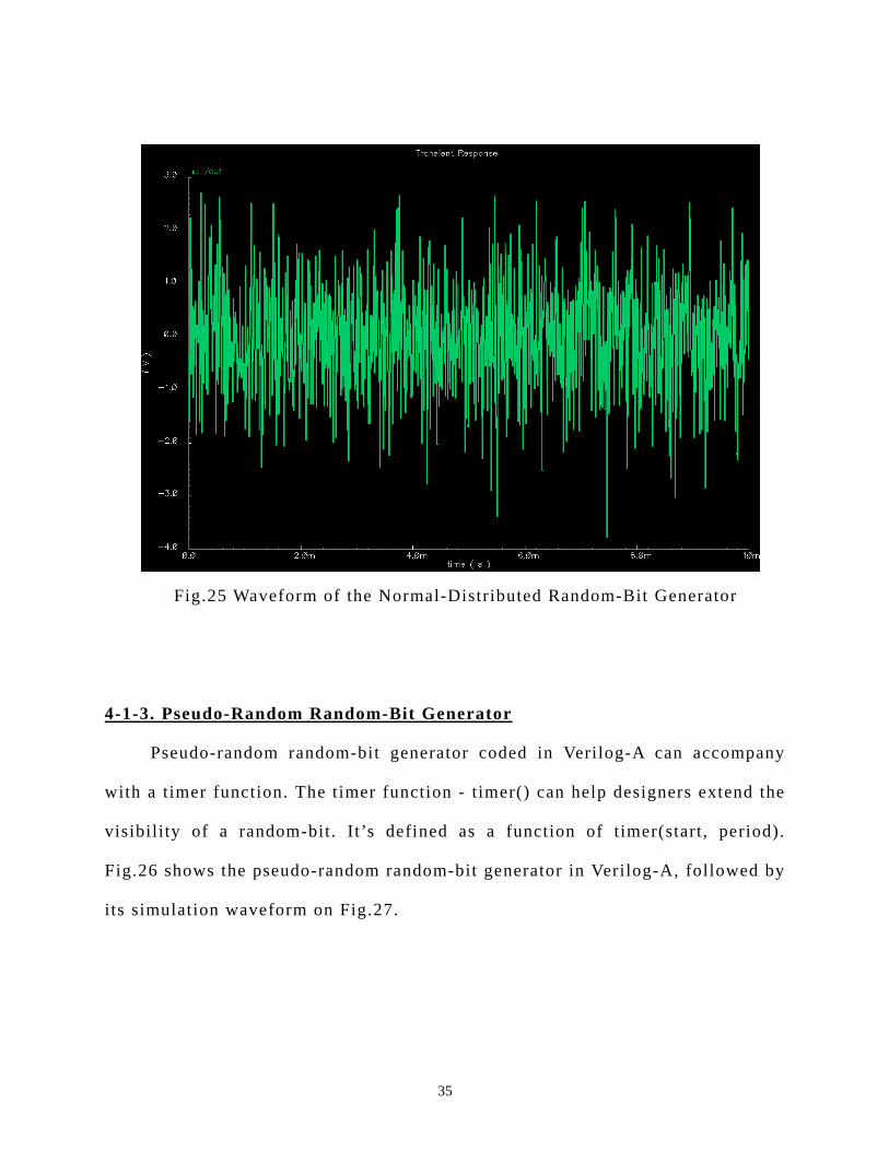
Fig.25 Waveform of the Normal-Distributed Random-Bit Generator
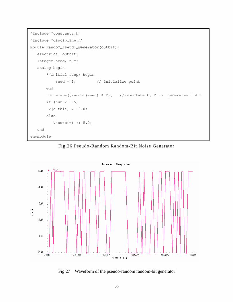
4-1-3. Pseudo-Random Random-Bit Generator
in Verilog-A can accompany
with
Pseudo-random random-bit generator coded
a timer function. The timer function - timer() can help designers extend the
visibility of a random-bit. It’s defined as a function of timer(start, period).
Fig.26 shows the pseudo-random random-bit generator in Verilog-A, followed by
its simulation waveform on Fig.27.
35
Fig.26 Pseudo-Random Random-Bit Noise Generator
Fig.27 Waveform of the pseudo-random random-bit generator
`include "constants.h"
rator(outbit);
begin
/ initialize point
e by 2 to generates 0 & 1
;
`include "discipline.h"
module Random_Pseudo_Gene
electrical outbit;
integer seed, num;
analog begin
step) @(initial_
seed = 1; /
end
abs($random(seed) % 2); //imodulat num =
if (num < 0.5)
V(outbit) <+ 0.0;
else
tbit) <+ 5.0 V(ou
end
e endmodul
36
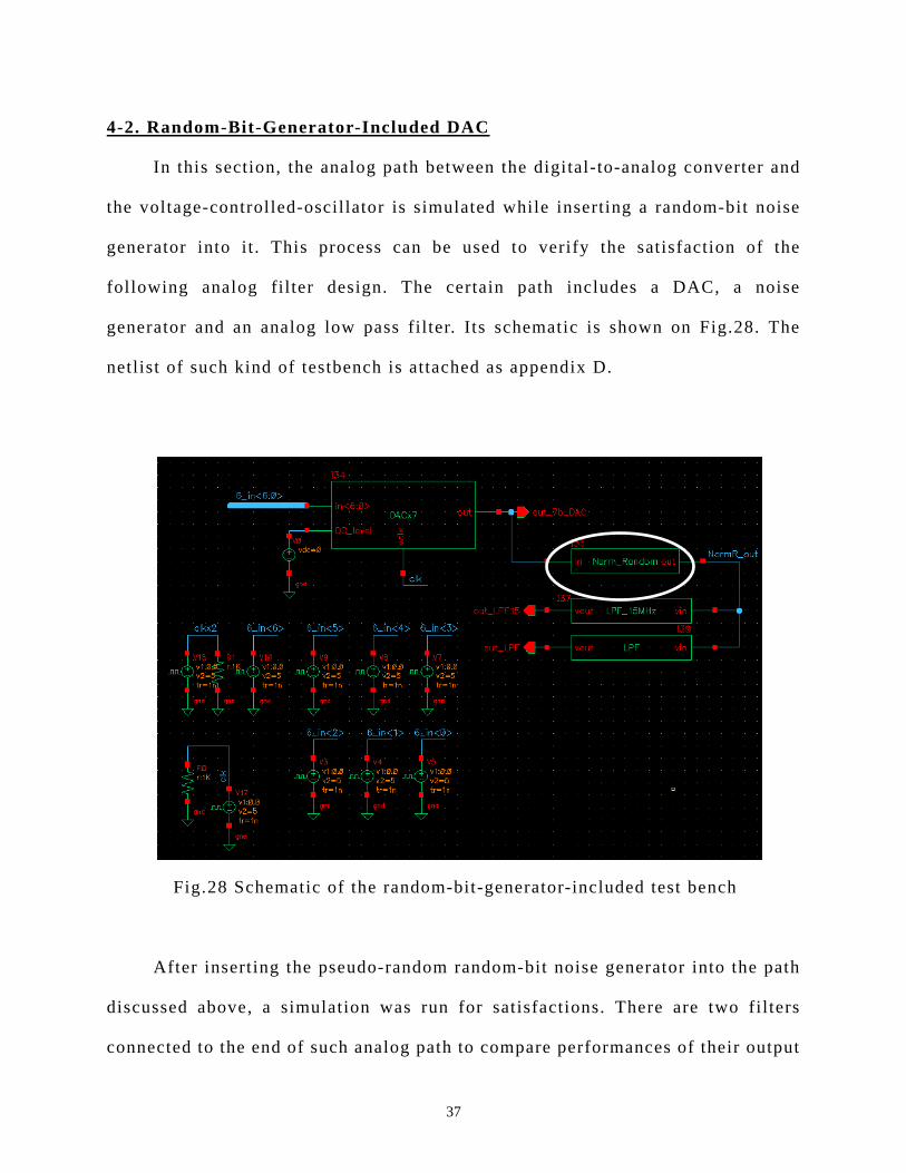
4-2. Random-Bit-Generator-Included DAC
i tal-to-analog converter and
the vo
Fig.28 Schematic of the random-bit-generator-included test bench
After inserting the pseu -random random-bit noise generator into the path
discussed
connected to the end of such analog path to compare performances of their output
In this section, the analog path between the dig
ltage-controlled-oscillator is simulated while inserting a random-bit noise
generator into it . This process can be used to verify the satisfaction of the
following analog filter design. The certain path includes a DAC, a noise
generator and an analog low pass filter. Its schematic is shown on Fig.28. The
netlist of such kind of testbench is attached as appendix D.
do
above, a simulation was run for satisfactions. There are two filters
37
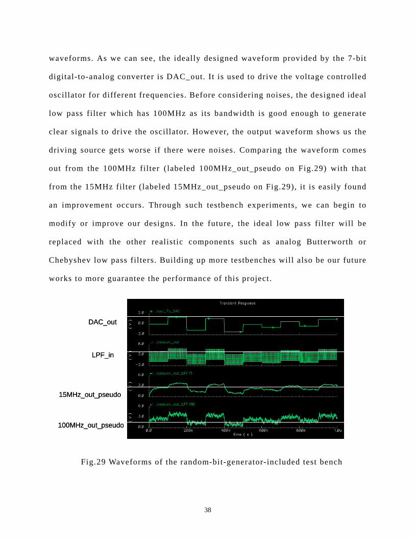
waveforms. As we can see, the ideally designed waveform provided by the 7-bit
digital-to-analog converter is DAC_out. It is used to drive the voltage controlled
oscillator for different frequencies. Before considering noises, the designed ideal
low pass fil ter which has 100MHz as its bandwidth is good enough to generate
clear signals to drive the oscillator. However, the output waveform shows us the
driving source gets worse if there were noises. Comparing the waveform comes
out from the 100MHz filter (labeled 100MHz_out_pseudo on Fig.29) with that
from the 15MHz filter (labeled 15MHz_out_pseudo on Fig.29), it is easily found
an improvement occurs. Through such testbench experiments, we can begin to
modify or improve our designs. In the future, the ideal low pass filter will be
replaced with the other realistic components such as analog Butterworth or
Chebyshev low pass filters. Building up more testbenches will also be our future
works to more guarantee the performance of this project.
Fig.29 Waveforms of the random-bit-generator-included test bench
100MHz_out_pseudo
15MHz_out_pseudo
DAC_out
LPF_in
100MHz_out_pseudo
15MHz_out_pseudo
DAC_out
LPF_in
38
Chapter 5
Entire DPLL Design and Simulation
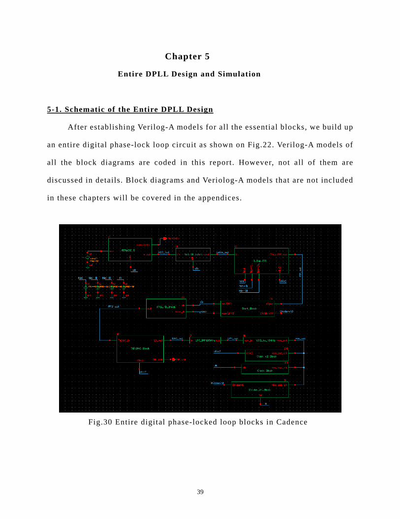
5-1. Schematic of the Entire DPLL Design
After establishing Verilog-A models for all the essential blocks, we build up
own on Fig.22. Verilog-A models of
all th
an entire digital phase-lock loop circuit as sh
e block diagrams are coded in this report. However, not all of them are
discussed in details. Block diagrams and Veriolog-A models that are not included
in these chapters will be covered in the appendices.
Fig.30 Entire digital phase-locked loop blocks in Cadence
39
5-2. S mulation Waveform of the Entire DPLL Designi
unning simulation by means of the Cadence Analog Artist simulator, we
system level Verilog-A
DPLL
R
get the simulation results presented on Fig.23 for the
circuit. As we can see, the output voltage of LPF_out is reset to zero volts
at 8.5us, after that time the correct output will begin to produce out. The
oscillating frequency, vco_out, changes its value whenever the plus or minus
signal presents. Within a certain lock-in time, we are confident that the
phase-locked loop will become stable and synchronize to the frequency of input
signal that comes in from the hard-disk.
Vin
Vref
Minus
Plus
VCO
LPF_out
PFD_out
Vin
Vref
Minus
Plus
VCO
LPF_out
PFD_ t
Fig.31 Waveform of the entire DPLL
ou
40
Chapter 6
Conclusion
According to the system- -A models and simulations presented
in th eport, we can recognize several advantages of Verilog-A. First, due to
that
level Verilog
is r
implementing system-level designs and simulations are necessary for the
modern complicated mixed signal circuits. Verilog-A becomes a very excellent
choice to accomplish this task. Second, modeling in Verilog-A the behavior
functions of a block that is going to be designed is fully compatible with Verilog,
a pure digital hardware design description language. We can take their merits
such as fast design, easy to debug in software and reusable ability in the whole
design process. The future capability for automatic synthesis is also becoming
one of the most important goals of Verilog-A. Many of the other characteristics
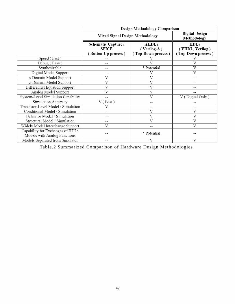
and advantages are listed in Table.2. Also a practical design of the Verilog-A
digital phase-locked-loop circuit is experienced in this report to convince
designers about the compatibilities of Verilog-A in Cadence environment as well .
41
Table.2 Summarized Comparison of Hardware Design Methodologies