A Universal Small Signal Class A Buffer www.hifisonix.com A Universal Small Signal Class A Buffer This article presents a simple, foolproof way to create a high performance Class A buffer that addresses concerns about op‐amp outputs transitioning from class A to class B operation into heavy output loads leading to signal degradation, and the production of unwanted higher order harmonics. Further, if all the stages in the small signal chain can be guaranteed to run in class A, there will be benefits to gain through the reduction of half wave signal currents in the power supply rails and the associated harmonics. 5ppm at 10V RMS into 600 Ohms is easily achievable, while at a more normal signal level of 2 VRMS into 600 Ohms, 3ppm distortion 20Hz to 20KHz is attainable. Both a high power (Iq = 110mA) and a low power (Iq=65mA) version are discussed. This buffer can also be applied as a class A headphone amplifier, where it will deliver 3V into a 32 Ohm load whilst still remaining in Class A at below 5ppm distortion 20Hz to 20KHz. Andrew C. Russell January 2011
Transcript
A Universal Small Signal Class A Buffer
www.hifisonix.com Page 1
A Universal Small Signal Class ABuffer
This article presents a simple, foolproof way to create a high performance Class A buffer that addresses concerns about op‐amp outputs transitioning from class A to class B operation into heavy output loads leading to signal degradation, and the production of unwanted higher order harmonics. Further, if all the stages in the small signal chain can be guaranteed to run in class A, there will be benefits to gain through the reduction of half wave signal currents in the power supply rails and the associated harmonics. 5ppm at 10V RMS into 600 Ohms is easily achievable, while at a more normal signal level of 2 VRMS into 600 Ohms, 3ppm distortion 20Hz to 20KHz is attainable. Both a high power (Iq = 110mA) and a low power (Iq=65mA) version are discussed. This buffer can also be applied as a class A headphone amplifier, where it will deliver 3V into a 32 Ohm load whilst still remaining in Class A at below 5ppm distortion 20Hz to 20KHz.
Andrew C. Russell
January 2011
A Universal Small Signal Class A Buffer
www.hifisonix.com Page 2
A Universal Small Signal
Class A Buffer with Short Circuit Protection
One of the criticisms leveled at IC op‐amps is the fact that beyond very small load currents (perhaps 1‐2mA) their outputs operate in class B. The generally very good distortion performance of these devices soon dissipates as the output load current increases. There are a few devices which stand out and manage to still deliver good performance with heavy output loads, but they a few and far between – examples being the LM4562 and its stable mates, some of the ADI offerings and of course the SA5534/32. However, often this performance is achieved through the use of very large amounts of feedback. I am not an anti‐feedback or zero feedback proponent, but it seems to me that what is needed is a cure for the root cause problem, rather than the treatment of the symptom which is that class B output stage.
At this point, you may be wondering why semiconductor manufacturers don’t just give audio fanatics what they want ‐ a solid class A op‐amp which would address all our concerns. Well, the applications and marketing folks that specify these things would tell us there’s no need: it takes c. 2VRMS to drive a power amp (almost any power amp you care to name) to full power with a typical input impedance of 10k Ohms and most op‐amps will be solidly in class A at these levels with the peak output current below 300uA. Any decent audio op‐amp can do that at <10 ppm distortion out to 20KHz (the SA5532/4 was doing that 30 years ago). Maybe an RIAA amp’s requirements are a bit stiffer because it has to drive a feedback network whose impedance drops precipitously as frequency increases, but there’s not many of those around, and in the big scheme of things, their days are numbered anyway. What about driving a pair of 32 Ohm headphone’s? Please see our catalog for dedicated headphone drivers is the answer you’d get. Power consumption and package costs are also a critical factor. How many class A op‐amps could they sell every year? Almost certainly not enough to make it worth it. Who would be the first to specify bigger PSU’s to accommodate the higher standing currents? We have to conclude that if we want a class A output op‐amp, we will have to ‘roll our own’. We could go ‘all discrete’ here, but that would mean added complexity, and almost certainly would not perform better than an IC op‐amp if all the specifications were considered (DC offset, noise, distortion, PSSR etc).
Fig 1 shows a very simple class A buffer that addresses all of the shortcomings of IC op‐amps for applications where greater drive current along with fidelity are required. This design is simpler than competing diamond buffer designs, and still achieves outstanding performance.
The op‐amp drives an emitter follower, Q1, which is loaded by an ~100mA constant current source (57mA in the low power version) formed by Q2, D1, D2 and R12. Q3 and R6 form a 5mA load for the driving op‐amp U1, which forces it to operate in Class A over its full output voltage range. R4 and C1 provide loop compensation, and C1 must be tailored according to the op‐amp being used (U1). For fast op‐amps, a higher value will be required in order to prevent HF oscillation. Note that this circuit is only suitable for unity gain stable op‐amps – but more of this later.
A Universal Small Signal Class A Buffer
www.hifisonix.com Page 3
Since Q1 is loaded with a current source, the current through loads being pulled –ve with respect to 0V is limited to ~100mA. In the positive direction, D3, D4 and R3 form a ‘flying clamp’ current limiter. Originally I had only D4 fitted, however, during measurement on the physical prototype (to be discussed later), this approach introduced significant amounts of distortion, starting as low as 1V RMS out, and this design error was corrected by adding an additional diode, D3, in series with D4. The resulting current limit is substantially higher on the +ve half cycle swing at ~300mA (the ‐ve half cycle swing is about 104mA). With that done, the distortion performance predicted in LTSpice was achieved.
R2 is a stopper resistor, and must be placed as close to Q1’s base as possible.
Note that R11 is just a holding resistor to aid in design – its not used in practical physical design, and in the simulator, has no effect.
IC op‐amps do not drive capacitive loads very well directly from their outputs, and well engineered designs always incorporate a 50 Ohm resistor between the op‐amp output and the load in order to isolate the op‐amp from any possible capacitive load. In this buffer design, R3 (3.3 Ohms) and R7 (10 Ohms) serves to isolate the buffer from capacitive loads on the output, and this buffer will happily drive any capacitive load without running into stability problems. Of course, if you really are after 0 Ohms output impedance, you will need to limit the input signal bandwidth by increasing either R5, C2 or both, but this is not recommended practice. For normal usage like driving hi‐fi cables or headphones, you can safely run this pre‐amp with only 6.6 Ohms series output resistance (this is R3+R7 in the Fig 1 and Fig 2 schematics), where the buffer will tolerate up to 10nF and still remain perfectly stable.
The simulator design work was done using a Linear Tech LT1115 device, but any high performance audio op‐amp will work in this circuit provided a few simple guidelines are followed:‐
1. Use a unity gain stable op‐amp for U1. You may not use de‐compensated op‐amps in this design (i.e. non unity gain stable op‐amps).
2. You can use uncompensated op‐amps like the SA5534A, but you will then have to select a suitable compensation cap (this fits directly across pins 8 and 5 on the SA5534 so don’t confuse this with C1 in the circuit diagram of Fig 1 which has a different purpose). This cap should be selected based on data sheet guidelines for unity gain operation.
3. For op‐amps that are considerably faster than the LT1115 shown here, you will need to adjust the value of C1, the loop compensation capacitor, to ensure stability. The best way to do this is to start with a high value – e.g. 220pF, and feeding a 10‐20KHz 1V pk to pk signal on the input, look at the output of the buffer and reduce the value of C1 until you get a perfect square wave. If you start to note any overshoot, that’s a sure indication that you have reduced the value of C1 too much. Note that this step (step 3) must only be done after you have completed step 2 if you are using an uncompensated op‐amp.
4. You may not use this design as it stands with Current Feedback Op‐Amps. The compensation scheme shown is not suitable for CFA’s and the buffer will oscillate and have stability problems.
A Universal Small Signal Class A Buffer
www.hifisonix.com Page 4
In the physical prototype to be dissected a little further on, I successfully used a National Semi LM4562 op‐amp without any changes to the compensation values shown.
Figure 1 – Simple, Universal Class A Buffer (High Power Version Shown)
Lower Power Class A Operation
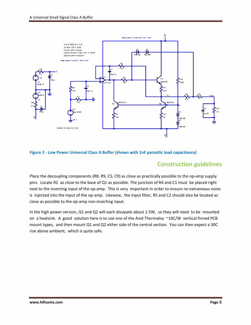
If you are unlikely to ever encounter anything below 600 Ohms, it is quite permissible to reduce the Class A standing current, and here I tried a figure of 57mA by setting R12 to 12 Ohms, and R3 to 5.6 Ohms, rather than the 6.8 Ohms and 3.3 Ohms respectively and this is shown in Fig 2. The simulated performance is as good, with 1V RMS 20KHz distortion at 3ppm, and 10V RMS into 600 Ohms coming in at 15ppm. Running at lower power of course means you can reduce the size of the heatsink considerably or even dispense with it completely if you place enough copper land down on your PCB.
A Universal Small Signal Class A Buffer
www.hifisonix.com Page 5
Figure 2 ‐ Low Power Universal Class A Buffer (shown with 1nF parasitic load capacitance)
Construction guidelines
Place the decoupling components (R8, R9, C5, C9) as close as practically possible to the op‐amp supply pins. Locate R2 as close to the base of Q1 as possible. The junction of R4 and C1 must be placed right next to the inverting input of the op‐amp. This is very important in order to ensure no extraneous noise is injected into the input of the op‐amp. Likewise, the input filter, R5 and C2 should also be located as close as possible to the op‐amp non‐inverting input.
In the high power version, Q1 and Q2 will each dissipate about 1.5W, so they will need to be mounted on a heatsink. A good solution here is to use one of the Avid Thermaloy ~10C/W vertical finned PCB mount types, and then mount Q1 and Q2 either side of the central section. You can then expect a 30C rise above ambient, which is quite safe.
A Universal Small Signal Class A Buffer
www.hifisonix.com Page 6
Figure 3 – LTSpice FFT of the Low Power Universal Buffer. 1VRMS into 600 Ohms
2nd Harmonic distortion is ‐118dB, while 3rd and 4th are below ‐130db and higher order harmonics are below ‐180dB.
Measured ‐3dB frequency response was considerably better than simulated (here ‐3dB at about 1.5MHz), but this was due to the use of a different op‐amp (LT115in the sim vs LM4562 in the physical prototype)
Figure 4 ‐ Low Power Universal Buffer Frequency Response into 600 Ohms
Figure 5 ‐ Universal Buffer Low Power Version 100KHz Square Wave Performance
1uV level ref 1V RMS
A Universal Small Signal Class A Buffer
www.hifisonix.com Page 7
Testing and Measuring the Prototype
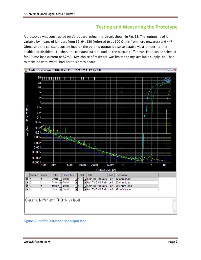
A prototype was constructed on Veroboard using the circuit shown in Fig. 13. The output load is variable by means of jumpers from 32, 64, 550 (referred to as 600 Ohms from here onwards) and 4k7 Ohms, and the constant current load on the op‐amp output is also selectable via a jumper – either enabled or disabled. Further, the constant current load on the output buffer transistor can be selected for 100mA load current or 57mA. My choice of resistors was limited to my available supply, so I had to make do with what I had for this proto board.
Figure 6 ‐ Buffer Distortion vs Output load
A Universal Small Signal Class A Buffer
www.hifisonix.com Page 8
Note that for all these measurements, a supply of +‐18V was used, and tests were done in the high power mode ‐ i.e. 104mA load current on the output follower transistor, and the op‐amp constant current load was enabled.
Fig.6 details the buffer distortion performance into various loads, along with the AP reference (this is the DARK BLUE trace in Fig. 6). Firstly, given the series output resistance of 14 Ohms and the maximum output current of 104mA, the output into 32 Ohms is just over 3V, while into 62 Ohms its around 5V and into 600 Ohms about 12VRMS. Distortion below about 2V out into all the measured loads is around 6dB higher than the AP reference. Above about 2V output, there is little real difference between the AP reference plot and the buffer output.
Figure 7 ‐ Spectrum Analysis into Various Loads
A Universal Small Signal Class A Buffer
www.hifisonix.com Page 9
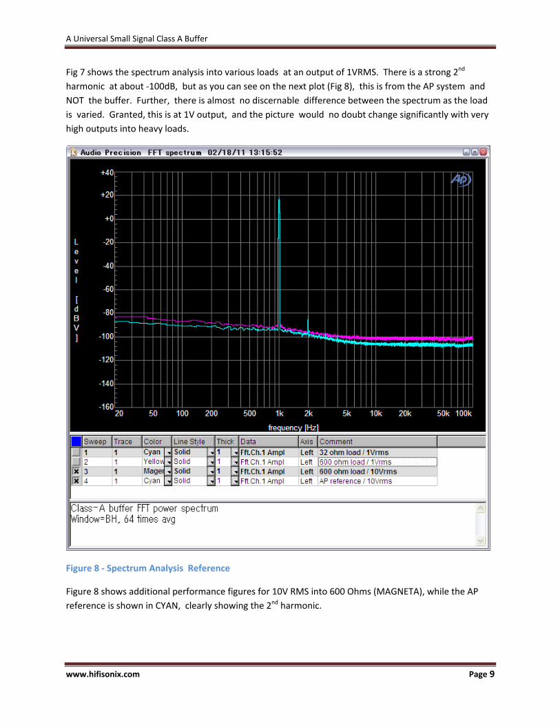
Fig 7 shows the spectrum analysis into various loads at an output of 1VRMS. There is a strong 2nd harmonic at about ‐100dB, but as you can see on the next plot (Fig 8), this is from the AP system and NOT the buffer. Further, there is almost no discernable difference between the spectrum as the load is varied. Granted, this is at 1V output, and the picture would no doubt change significantly with very high outputs into heavy loads.
Figure 8 ‐ Spectrum Analysis Reference
Figure 8 shows additional performance figures for 10V RMS into 600 Ohms (MAGNETA), while the AP reference is shown in CYAN, clearly showing the 2nd harmonic.
A Universal Small Signal Class A Buffer
www.hifisonix.com Page 10
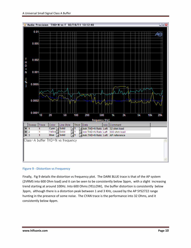
Figure 9 ‐ Distortion vs Frequency
Finally, Fig 9 details the distortion vs frequency plot. The DARK BLUE trace is that of the AP system (2VRMS into 600 Ohm load) and it can be seen to be consistently below 3ppm, with a slight increasing trend starting at around 100Hz. Into 600 Ohms (YELLOW), the buffer distortion is consistently below 3ppm, although there is a distortion peak between 1 and 3 KHz, caused by the AP SYS2722 range hunting in the presence of some noise. The CYAN trace is the performance into 32 Ohms, and it consistently below 4ppm.
A Universal Small Signal Class A Buffer
www.hifisonix.com Page 11
Conclusions
The Universal Small Signal Class A Buffer will usefully drive any load from c. 32 Ohms (and thus make a fine headphone amplifier) and higher at distortion levels well under 5ppm from 20Hz to 20KHz. It remains in class A mode into 32 Ohms, up to 3V output. Keep in mind here that normal headphone listening levels requires from c 300‐500mV. For output loads above 200 Ohms, the buffer will swing the load to over 10VRMS while still remaining in class A operation, with distortion below 5ppm all the way out to 20KHz. On 18V rails, the maximum undistorted output swing is in the region of 12V RMS into 600 Ohms.
Importantly, into heavy loads, the circuit maintains the same performance as a good op‐amp driving a light load, wherein the op‐amp output remains in class A. There is no doubt that the class A pre‐load directly on the op‐amps output helps here, although the use of the LM4562 with its outstanding linearity and loop gain plays a very significant part. The output distortion harmonics up to voltage swings within about 0.5V of the clipping level are all 2nd harmonic in this design – higher order components are below the AP SYS2722 noise floor. The buffer is stable into any capacitive load with an output resistance of c. 15 Ohms, although for normal domestic and headphone driver applications, it can be safely reduced to 6.6 Ohms (I have not tried lower output resistances, but this is easily confirmed if you have access to a scope and a square wave generator).
Figure 10 ‐ Universal Class A Buffer Proto Board
A Universal Small Signal Class A Buffer
www.hifisonix.com Page 12
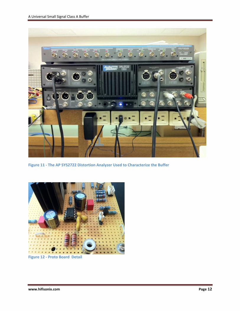
Figure 11 ‐ The AP SYS2722 Distortion Analyzer Used to Characterize the Buffer
Figure 12 ‐ Proto Board Detail
A Universal Small Signal Class A Buffer
www.hifisonix.com Page 13
Specifications
The distortion measurements below were taken on the prototype using the AP SYS2722 Audio Measurement System
Frequency Response DC to 4.5MHz (‐3dB) , 2VRMS into 600Ohms
Rise Time <0.2 us
Distortion (20Hz‐20KHz) <5ppm max (typically 3ppm) 2VRMS into 600 Ohms
2nd, 3rd and 4th and higher order harmonics all below AP SYS2772 noise floor (i.e. <<1.5ppm)
<3ppm at 1VRMS into 600 Ohms
<10ppm 10V RMS into 600 Ohms :
<5ppm 3VRMS into 32 Ohms
Noise Better than –120dB
Input Impedance 10k Ohms//100pF
Output Impedance 6.6 Ohms at 1KHz
Unconditionally stable
Supply +‐18V at 120mA per rail – High Power Version
+‐18V at 70mA per rail – Low Power Version
A Universal Small Signal Class A Buffer
www.hifisonix.com Page 1
Figure
13 ‐ Prototype Circuit as Built
Q3 and Q3 mounted on 10 degC/Wvertical mount heatsink
Link J3 to enable CC load on U1 OutputLink J1/J2 to select output loadLink J4 to change Q2 CC load from 57mAto 104mALink J5 to reduve series output isolation resistord from 14.1 Ohms to 3.3 Ohms