Page 1
A VERIOG-HDL IMPLEMENTATION OF VIRTUAL CHANNELS IN A
NETWORK-ON-CHIP ROUTER
A Thesis
by
SUNGHO PARK
Submitted to the Office of Graduate Studies ofTexas A&M University
in partial fulfillment of the requirements for the degree of
MASTER OF SCIENCE
August 2008
Major Subject: Computer Engineering
brought to you by COREView metadata, citation and similar papers at core.ac.uk
provided by Texas A&M University
Page 2
A VERIOG-HDL IMPLEMENTATION OF VIRTUAL CHANNELS IN A
NETWORK-ON-CHIP ROUTER
A Thesis
by
SUNGHO PARK
Submitted to the Office of Graduate Studies ofTexas A&M University
in partial fulfillment of the requirements for the degree of
MASTER OF SCIENCE
Approved by:
Chair of Committee, Peng LiCommittee Members, Eun Jung Kim
Gwan ChoiHead of Department, Costas N. Georghiades
August 2008
Major Subject: Computer Engineering
Page 3
iii
ABSTRACT
A Verilog-HDL Implementation of Virtual Channels in a Network-on-Chip Router.
(August 2008)
Sungho Park, B.E., Inha University
Chair of Advisory Committee: Dr. Peng Li
As the feature size is continuously decreasing and integration density is increas-
ing, interconnections have become a dominating factor in determining the overall
quality of a chip. Due to the limited scalability of system bus, it cannot meet the
requirement of current System-on-Chip (SoC) implementations where only a limited
number of functional units can be supported. Long global wires also cause many
design problems, such as routing congestion, noise coupling, and difficult timing clo-
sure. Network-on-Chip (NoC) architectures have been proposed to be an alternative
to solve the above problems by using a packet-based communication network. The
processing elements (PEs) communicate with each other by exchanging messages over
the network and these messages go through buffers in each router. Buffers are one of
the major resource used by the routers in virtual channel flow control.
In this thesis, we analyze two kinds of buffer allocation approaches, static and
dynamic buffer allocations. These approaches aim to increase throughput and mini-
mize latency by means of virtual channel flow control. In statically allocated buffer
architecture, size and organization are design time decisions and thus, do not perform
optimally for all traffic conditions. In addition, statically allocated virtual channel
consumes a waste of area and significant leakage power. However, dynamic buffer al-
location scheme claims that buffer utilization can be increased using dynamic virtual
channels. Dynamic virtual channel regulator (ViChaR), have been proposed to use
centralized buffer architecture which dynamically allocates virtual channels and buffer
Page 4
iv
slots in real-time depending on traffic conditions. This ViChaR’s dynamic buffer man-
agement scheme increases buffer utilization, but it also increases design complexity. In
this research, we reexamine performance, power consumption, and area of ViChaR’s
buffer architecture through implementation. We implement a generic router and a
ViChaR architecture using Verilog-HDL. These RTL codes are verified by dynamic
simulation, and synthesized by Design Compiler to get area and power consumption.
In addition, we get latency through Static Timing Analysis. The results show that a
ViChaR’s dynamic buffer management scheme increases the latency and power con-
sumption significantly even though it could increase buffer utilization. Therefore, we
need a novel design to achieve high buffer utilization without a loss.
Page 5
v
To my family for their love and encouragement.
Page 6
vi
ACKNOWLEDGMENTS
I would like to thank my research advisor, Dr. Eun Jung Kim, for her support,
encouragement and guidance during the period of my studies. She taught me a lot
about research and guided me through every step of my studies. I would also like to
thank chair, Dr. Peng Li, for his kindness, understanding and valuable comments. My
sincere thanks to Dr. Gwan Choi for his willingness to be on my defense committee
and his valuable comments. I would like to extend my special thanks to my colleague,
Manhee Lee. During this project, he was my partner in designing a network-on-chip
router. I thank him for his moral and technical support. Special thanks to my family
for their support and kindness. Sincere thanks to all my friends for their friendship
and support throughout the period of my studies at Texas A&M University.
Page 7
vii
TABLE OF CONTENTS
CHAPTER Page
I INTRODUCTION . . . . . . . . . . . . . . . . . . . . . . . . . . 1
II RELATED WORK . . . . . . . . . . . . . . . . . . . . . . . . . 4
A. Network-on-Chip Topology . . . . . . . . . . . . . . . . . . 4
B. Routing Strategy . . . . . . . . . . . . . . . . . . . . . . . 4
C. Dynamic Virtual Channel Allocation . . . . . . . . . . . . 5
III BACKGROUND . . . . . . . . . . . . . . . . . . . . . . . . . . 7
A. Network Property . . . . . . . . . . . . . . . . . . . . . . . 7
1. Topology . . . . . . . . . . . . . . . . . . . . . . . . . 7
2. Switching Technique . . . . . . . . . . . . . . . . . . . 8
3. Routing Protocol . . . . . . . . . . . . . . . . . . . . . 11
4. Flow Control Mechanism . . . . . . . . . . . . . . . . 12
B. Buffering in Packet Switches . . . . . . . . . . . . . . . . . 13
1. Output Queues . . . . . . . . . . . . . . . . . . . . . . 13
2. Input Queues . . . . . . . . . . . . . . . . . . . . . . . 14
3. Shared Central Queues . . . . . . . . . . . . . . . . . 14
C. Diverse Input Port Buffers . . . . . . . . . . . . . . . . . . 16
1. Single Input Queues . . . . . . . . . . . . . . . . . . . 16
2. SAFC (Statically Allocated Fully Connected) . . . . . 16
3. SAFQ (Statically Allocated Multi-Queue) . . . . . . . 16
4. SAFQ (Statically Allocated Multi-Queue) . . . . . . . 17
D. Generic NoC Router . . . . . . . . . . . . . . . . . . . . . 18
E. Dynamic Virtual Channel Regulator(ViChaR) . . . . . . . 18
1. ViChaR Configuration . . . . . . . . . . . . . . . . . . 18
2. Virtual Channel Allocator and a Switch Allocator . . 20
3. Register-Based Buffering . . . . . . . . . . . . . . . . 22
IV DESIGN FLOW . . . . . . . . . . . . . . . . . . . . . . . . . . . 23
A. Standard Cell Design . . . . . . . . . . . . . . . . . . . . . 23
1. Design Library . . . . . . . . . . . . . . . . . . . . . . 23
2. Hardware Description Language . . . . . . . . . . . . 23
B. Synthesis with Synopsys Design Compiler . . . . . . . . . . 24
Page 8
viii
CHAPTER Page
C. Design Evaluation Techniques . . . . . . . . . . . . . . . . 25
1. Throughput and Latency . . . . . . . . . . . . . . . . 25
2. Area Estimation . . . . . . . . . . . . . . . . . . . . . 25
3. Power Consumption Measurement . . . . . . . . . . . 25
V ROUTER IMPLEMENTATION . . . . . . . . . . . . . . . . . . 26
A. Asynchronous Design . . . . . . . . . . . . . . . . . . . . . 26
1. No Clock Skew . . . . . . . . . . . . . . . . . . . . . . 26
2. Low Power Consumption . . . . . . . . . . . . . . . . 26
3. Low Global Wire Delay . . . . . . . . . . . . . . . . . 26
4. Automatic Adaptation to Variation . . . . . . . . . . 27
B. An Arbiter Design . . . . . . . . . . . . . . . . . . . . . . 27
1. Basic Concept of Arbitration . . . . . . . . . . . . . . 27
2. Fixed Priority Arbiter . . . . . . . . . . . . . . . . . . 28
3. Round-Robin Arbiter . . . . . . . . . . . . . . . . . . 29
4. Matrix Arbiter . . . . . . . . . . . . . . . . . . . . . . 30
5. Tree Arbiter . . . . . . . . . . . . . . . . . . . . . . . 31
C. A Generic Router . . . . . . . . . . . . . . . . . . . . . . . 32
1. High-level View . . . . . . . . . . . . . . . . . . . . . 32
2. Buffer Architecture . . . . . . . . . . . . . . . . . . . 33
3. Virtual Channel Allocator(VA) . . . . . . . . . . . . . 36
4. Switch Allocator(SA) . . . . . . . . . . . . . . . . . . 36
5. Crossbar Switch and Other Implementation . . . . . . 39
D. A Virtual Channel Regulator . . . . . . . . . . . . . . . . 39
1. High-level View . . . . . . . . . . . . . . . . . . . . . 39
2. Buffer Architecture . . . . . . . . . . . . . . . . . . . 42
3. Virtual Channel Allocator(VA) . . . . . . . . . . . . . 46
4. Switch Allocator(SA) . . . . . . . . . . . . . . . . . . 46
5. VC/Slot Availability Tracker . . . . . . . . . . . . . . 48
6. VC Control Table . . . . . . . . . . . . . . . . . . . . 48
7. Crossbar Switch in a ViChaR . . . . . . . . . . . . . . 50
VI RESULT AND OTHER DISCUSSION . . . . . . . . . . . . . . 52
A. Area Estimation . . . . . . . . . . . . . . . . . . . . . . . . 52
1. Cell Area . . . . . . . . . . . . . . . . . . . . . . . . . 52
2. Interconnect and Total Area . . . . . . . . . . . . . . 53
B. Power Consumption Estimation . . . . . . . . . . . . . . . 54
1. Dynamic Power Consumption . . . . . . . . . . . . . . 55
Page 9
ix
CHAPTER Page
2. Cell Leakage Power Consumption . . . . . . . . . . . . 55
C. Latency Estimation . . . . . . . . . . . . . . . . . . . . . . 56
VII CONCLUSION AND FUTURE WORK . . . . . . . . . . . . . . 64
A. Conclusion . . . . . . . . . . . . . . . . . . . . . . . . . . . 64
B. Future Work . . . . . . . . . . . . . . . . . . . . . . . . . . 65
REFERENCES . . . . . . . . . . . . . . . . . . . . . . . . . . . . . . . . . . . 66
APPENDIX A . . . . . . . . . . . . . . . . . . . . . . . . . . . . . . . . . . . 69
APPENDIX B . . . . . . . . . . . . . . . . . . . . . . . . . . . . . . . . . . . 74
APPENDIX C . . . . . . . . . . . . . . . . . . . . . . . . . . . . . . . . . . . 79
VITA . . . . . . . . . . . . . . . . . . . . . . . . . . . . . . . . . . . . . . . . 82
Page 10
x
LIST OF TABLES
TABLE Page
I Total Cell Area (TSMC 180nm), G:Generic, V:ViChaR . . . . . . . . 53
II Net Interconnect Area (TSMC 180nm), G:Generic, V:ViChaR . . . . 53
III Total Area (TSMC 180nm), G:Generic, V:ViChaR . . . . . . . . . . 53
IV Dynamic Power Consumption (TSMC 180nm), G:Generic, V:ViChaR 56
V Leakage Power Consumption (TSMC 180nm), G:Generic, V:ViChaR 56
Page 11
xi
LIST OF FIGURES
FIGURE Page
1 Virtual Channel Router . . . . . . . . . . . . . . . . . . . . . . . . . 2
2 Example of Four Network Topologies . . . . . . . . . . . . . . . . . . 8
3 Store-and-Forward Switching Technique . . . . . . . . . . . . . . . . 9
4 Virtual Cut-Through Switching Technique . . . . . . . . . . . . . . . 10
5 The Concept of Virtual Channels . . . . . . . . . . . . . . . . . . . . 11
6 Unit of Resource Allocation . . . . . . . . . . . . . . . . . . . . . . . 12
7 Head-of-Line Blocking . . . . . . . . . . . . . . . . . . . . . . . . . . 14
8 Alternative Designs of Switching with Input Port Buffers . . . . . . . 15
9 Generic NoC Router Architecture . . . . . . . . . . . . . . . . . . . . 17
10 Buffer Architecture and Allocation . . . . . . . . . . . . . . . . . . . 19
11 Virtual Channel Allocation and Switch Allocation . . . . . . . . . . 21
12 Basic Synthesis Flow with Design Compiler . . . . . . . . . . . . . . 24
13 Example of Arbitration in FIFO . . . . . . . . . . . . . . . . . . . . 28
14 Example of a Fixed Priority Arbiter Code . . . . . . . . . . . . . . . 29
15 Muxed Parallel Arbiter . . . . . . . . . . . . . . . . . . . . . . . . . . 30
16 Two Fixed Priority Arbiters with a Mask . . . . . . . . . . . . . . . 30
17 Matrix Arbiter . . . . . . . . . . . . . . . . . . . . . . . . . . . . . . 31
18 Tree Arbiter . . . . . . . . . . . . . . . . . . . . . . . . . . . . . . . . 31
19 Top View of a Generic Router . . . . . . . . . . . . . . . . . . . . . . 34
Page 12
xii
FIGURE Page
20 Buffer Architecture of a Generic Router . . . . . . . . . . . . . . . . 35
21 1-bit D-Latch and Enable Signals . . . . . . . . . . . . . . . . . . . . 36
22 Virtual Channel Allocator in a Generic Router . . . . . . . . . . . . 37
23 Switch Allocator in a Generic Router . . . . . . . . . . . . . . . . . . 40
24 Crossbar Switch in a Generic Router . . . . . . . . . . . . . . . . . . 41
25 Top View of a ViChaR . . . . . . . . . . . . . . . . . . . . . . . . . . 43
26 Unified Buffer Structure(UBS) in a ViChaR . . . . . . . . . . . . . . 44
27 Limitation of a Statically Assigned Buffer Organization . . . . . . . 45
28 Virtual Channel Allocator in a ViChaR . . . . . . . . . . . . . . . . 47
29 VC/Slot Availability Tracker . . . . . . . . . . . . . . . . . . . . . . 48
30 Switch Allocator in a ViChaR . . . . . . . . . . . . . . . . . . . . . . 49
31 VC Control Table . . . . . . . . . . . . . . . . . . . . . . . . . . . . 50
32 Crossbar Switch in a ViChaR . . . . . . . . . . . . . . . . . . . . . . 51
33 Total Cell Area Comparison (TSMC 180nm) . . . . . . . . . . . . . . 54
34 Net Interconnect Area Comparison (TSMC 180nm) . . . . . . . . . . 54
35 Total Area Comparison (TSMC 180nm) . . . . . . . . . . . . . . . . 55
36 Dynamic Power Consumption Comparison (TSMC 180nm) . . . . . . 57
37 Leakage Power Consumption Comparison (TSMC 180nm) . . . . . . 57
38 Generic and ViChaR NoC Router Pipeline . . . . . . . . . . . . . . 58
39 VA Critical Path Delay in a Generic Router . . . . . . . . . . . . . . 59
40 VA Critical Path Delay in a ViChaR Router . . . . . . . . . . . . . . 60
41 SA Critical Path Delay in a Generic Router . . . . . . . . . . . . . . 62
Page 13
xiii
FIGURE Page
42 SA Critical Path Delay in a ViChaR Router . . . . . . . . . . . . . . 63
43 Verilog code of Top module in a generic router . . . . . . . . . . . . 70
44 Partial verilog code of Buffer module in a generic router . . . . . . . 71
45 Partial verilog code of a Virtual Channel Allocator in a generic router 72
46 Partial verilog code of a Switch Allocator in a generic router . . . . . 73
47 Partial verilog code of Top module in a ViChaR router . . . . . . . . 75
48 Partial verilog code of Buffer module in a ViChaR router . . . . . . . 76
49 Partial verilog code of a Virtual Channel Allocator in a ViChaR router 77
50 Partial verilog code of a Switch Allocator in a ViChaR router . . . . 78
51 Verilog code of a crossbar in a generic and ViChaR router . . . . . . 80
52 Verilog code of a round-robin arbiter in a generic and ViChaR router 81
Page 14
1
CHAPTER I
INTRODUCTION
As the technology scales down, the gate delay decreases, but the wire delay increases
relatively and this global wire delay becomes the main factor which can decide the
overall performance. Difficult timing closure becomes the main problem among many
design issues which is caused by long global wire delay. Many VLSI designers are
trying to solve this long global wire delay problem through buffer insertion. In ad-
dition, many current System-on-Chips (SoCs) use a system bus to connect several
functional units. The slave unit would comply with this system bus protocol in or-
der to be synchronized with the master unit. However, these SoC system buses can
support only limited number of functional units, and thus will face scaling problems
in heterogeneous MPSoCs (MultiProcessor System-on-Chips) or large scale CMPs
(Chip-MultiProcessors). Even though a multiple bus structure with bridge and bus
matrix structure could be the alternative plans, these solutions still do not scale well
and have the disadvantages of high power consumption. In order to solve these long
global wire delay and scalability issues, many studies suggested the use of a packet-
based communication network which is known as Network-on-Chip (NoC). This NoC
is used to connect many functional units with a universal communication network
[1, 2, 3] .
In NoC, a router sends packets from a source to a destination router through
several intermediate nodes. If the head of packet is blocked during data transmission,
the router cannot transfer the packet any more. In order to remove the blocking
problem, the researcher proposed wormhole routing method. The wormhole router
The journal model is IEEE Transactions on Automatic Control.
Page 15
2
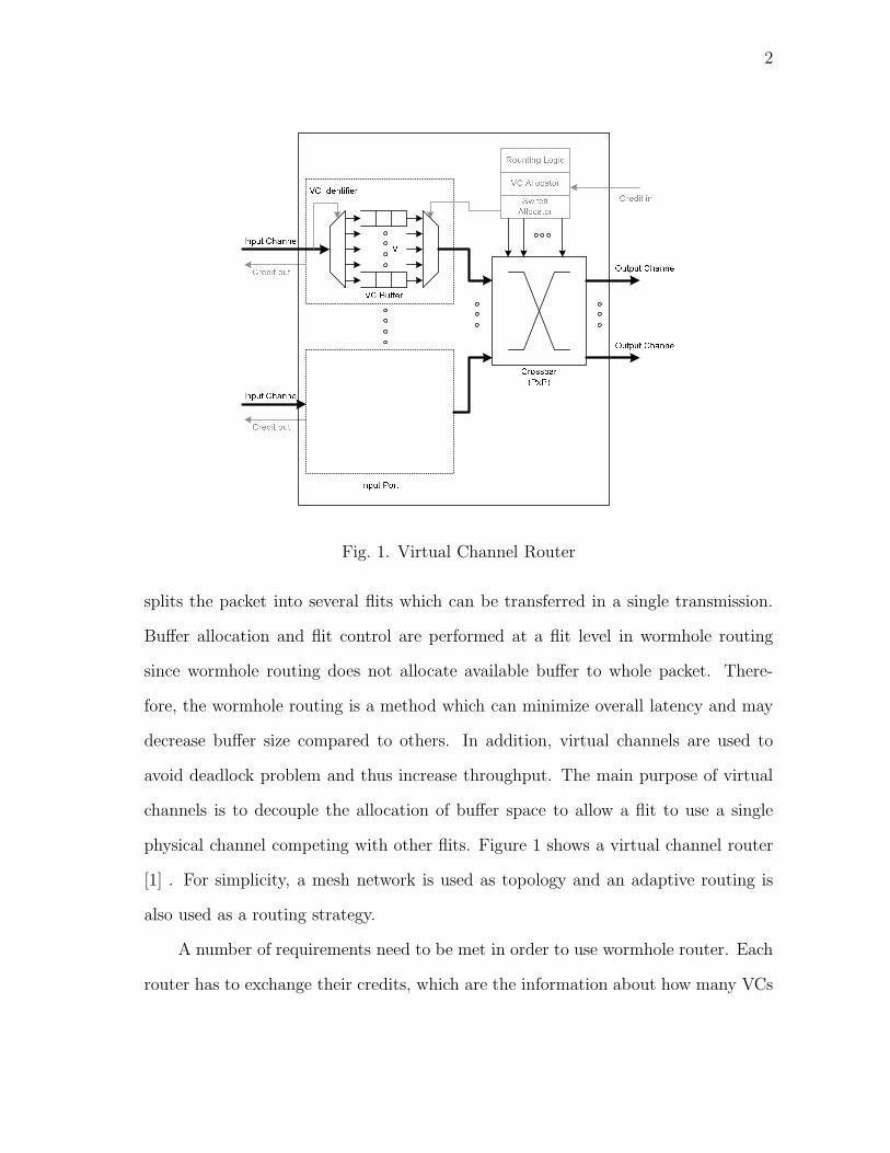
Fig. 1. Virtual Channel Router
splits the packet into several flits which can be transferred in a single transmission.
Buffer allocation and flit control are performed at a flit level in wormhole routing
since wormhole routing does not allocate available buffer to whole packet. There-
fore, the wormhole routing is a method which can minimize overall latency and may
decrease buffer size compared to others. In addition, virtual channels are used to
avoid deadlock problem and thus increase throughput. The main purpose of virtual
channels is to decouple the allocation of buffer space to allow a flit to use a single
physical channel competing with other flits. Figure 1 shows a virtual channel router
[1] . For simplicity, a mesh network is used as topology and an adaptive routing is
also used as a routing strategy.
A number of requirements need to be met in order to use wormhole router. Each
router has to exchange their credits, which are the information about how many VCs
Page 16
3
are available in the adjacent router. During establishing VCs among routers, each
router arbitrates candidate VCs with this credit information. The transmitting router
has to keep the credit information such as the number of available free buffers and
the number of available VCs from nearby routers. The receiving router also updates
the read/write pointers in internal buffer control logic when it receives the flit from
the previous router.
Buffers consume much leakage power since buffers, which are implemented with
registers, occupy large areas compared to other combinational logics [1] . From [4] the
buffers consume about 64 percent of the total router leakage power. Dynamic power
consumption is proportional to switching activity, supply voltage, and capacitance
load. Whenever the flit arrives at or departs from router, it consumes much dynamic
power depending on switch activity. Therefore, buffer design plays an important role
in implementing an energy efficient on-chip network. The goal of this thesis is to
provide a detailed explanation to implement generic and ViChaR (Virtual Channel
Regulator) structure. In Chapter II, we take a look at related work. Chapter III
presents the basic concept of virtual channels in a generic router, and Chapter IV
presents implementation methodology and Chapter V is a router implementation,
and Chapter VI is a conclusion of my work.
Page 17
4
CHAPTER II
RELATED WORK
This thesis draws on and builds on a variety of related and prior works in the area
of design of network-on-chip buffers, virtual channel allocation (VA) and switch al-
location (SA) in the router. Prior studies provide concepts and systems that will be
implemented and further refined in the course of the proposed research.
A. Network-on-Chip Topology
W. J. Dally introduced Network-on-Chip communication and especially 2D torus ar-
chitecture in [2]. Kumar et al. [5] used 2-D tile-based architecture adopting a mesh
based topology. Mesh and torus are popular NoC topologies, and they have different
features in terms of throughput, power consumption, and latency depending on rout-
ing algorithms [6]. In addition, SPIN network uses the fat tree topology in [3] and
octagon topology is proposed in [7]. Each topology has its own characteristic. Among
theses topologies, many designers like to use mesh topology because of simplicity.
B. Routing Strategy
The packet is routed through networks depending on a routing strategy. The routing
algorithms could be one of the following two strategies. Deterministic routing such
as XY routing is when the routes between given pairs of nodes are pre-programmed
and thus follow the same path between two nodes. Adaptive routing is when the
path taken by a packet may depend on other packets, and each router should know
network traffic status in order to avoid a congested region in advance [2].
Page 18
5
C. Dynamic Virtual Channel Allocation
A generic router generally uses a statistically allocated buffer which can cause the
Head-of-Line (HoL) blocking problem. [8] proposes buffer customization which de-
creases the queue blocking probability in order to improve the network performance.
A scheme called dynamic virtual channel regulator (ViChaR) is proposed in [9] . In
the ViChaR, VCs are allocated dynamically, and buffer allocation for each VC could
be different depending on network traffic. For example, many and shallow VCs are
more efficient in the light traffic, and few and deeper VCs are more efficient in heavy
traffic. In addition, on-chip network router meeting traffic demand must be designed
to have the least number of buffers since the power consumption of the buffer dom-
inates all the other logic such as VA, SA, and crossbar[9]. ViChaR proposes the
method of increasing buffer utilization and decreasing overall power consumption.
From [9] the area overhead and extra power consumption is trivial where there is a
4 percent reduction in logic area and minimal 2 percent power increase compared to
equal size generic buffer implementation. Especially, it reports a 25 percent increase
in performance with the same amount of buffering [9].
Dynamically Allocated Multi-Queue (DAMQ) buffer architecture is presented in
[10]. This DAMQ has the unified and dynamically-allocated buffer structure. The
concept of DAMQ is similar with ViChaR. DAMQ uses a fixed number of queues per
input port. But this can cause the HoL blocking problem. Therefore, ViChaR assigns
the buffer resource to each of the VCs according to the network traffic in order to
solve the HoL problem. Fully Connected Circular Buffer (FC-CB) is explained in [11].
FC-CS is basically using a Dynamically Allocated Fully Connected (DAFC) method
[12] in order to have the flexibility in diverse traffic by adapting wormhole routing
and virtual channels. Hence, this FC-CB provides a low average message latency and
Page 19
6
high throughput even under heavy traffic. However, FC-CB structure has a fixed
number of VCs and complex logic to control circular buffer and thus causes higher
dynamic power consumption.
Page 20
7
CHAPTER III
BACKGROUND
This chapter provides background information on Network-on-Chip research areas
throughout the thesis. On-chip networks share many concepts with an interconnection
network for a traditional multiprocessor system. When we categorize networks, it is
typically done by recognizing four key properties: topology, switching technique,
routing protocol, and flow control mechanism.
A. Network Property
1. Topology
Mesh and torus network topologies are selected as the best choice in a NoC [2]. These
two network topologies have simplicity of 2-D square structure. Figure 2 (a) shows
a 2-D mesh network structure [5]. It is composed of a grid of horizontal and vertical
lines with a router. This mesh topology is mostly used since delay among routers can
be predicted in a high level. A router address is computed by the number of horizontal
nodes and the number of vertical nodes. 2-D torus topology [2] is a donut-shaped
structure which is made by a 2-D mesh and connection of opposite sides as we can see
in Figure 2 (b). This topology has twice the bisection bandwidth of a mesh network
at the cost of a doubled wire demand. But the nodes should be interleaved because all
inter-node routers have the same length. In addition to the mesh and torus network
topologies, a fat-tree structure [3] is used. In M-ary fat-tree structure, the number
of connections between nodes increases with a factor M towards the root of the tree.
By wisely choosing the fatness of links, the network can be tailored to efficiently
use any bandwidth. An octagon network was proposed by [7]. Eight processors are
Page 21
8
(a) Mesh (b) Torus
(c) Binary Fat Tree (d) Octagon
Fig. 2. Example of Four Network Topologies
linked by an octagonal ring. The delays between any two nodes are no more than two
hops within the local ring. The advantage of an octagon network has scalability. For
example, if a certain node can be operated as a bridge node, more Octagon network
can be added using this bridge node. Figure 2 (c) and (d) show binary fat-tree and
octagon topologies.
2. Switching Technique
Switching mechanisms determine how network resources are allocated for data trans-
mission when the input channel is connected to the output channel selected by the
routing algorithm. There are typically four popular switching techniques: store-and-
forward, virtual cut-through, wormhole switching, and circuit switching [13]. The
first three techniques are categorized into a packet-switching method.
In a store-and-forward switching method, the entire packet has to be stored in
the buffer when a packet arrives at an intermediate router. After a packet arrives,
Page 22
9
Fig. 3. Store-and-Forward Switching Technique
the packet can be forwarded to a neighboring node which has available buffering
space, available to store the entire packet. This switching technique requires a lot
of buffering space more than the size of the largest packet. It should increase the
on-chip area. In addition to the area, it could cause large latency because a certain
packet cannot traverse to the next node until its whole packet is stored. Figure 3
shows a store-and-forward switching technique and a flow diagram.
In order to solve long latency problem in a store-and-forward switching scheme,
virtual cut-through switching [14] stores a packet at an intermediate node if next
routers are busy, while current node receives the incoming packet. But, it still requires
a lot of buffering space in the worst case. Figure 4 shows the timing diagram for a
virtual cut-through switching method.
The requirement of large buffering space can be solved using the wormhole switch-
ing method [15]. In the wormhole switching method, the packets are split to flow
control digits (flits) which are snaked along the route in a pipeline fashion. There-
fore, it does not need to have large buffers for the whole packets but has small buffers
for a few flits. A header flit build the routing path to allow other data flits to tra-
verse in the path. A disadvantage of wormhole switching is that the length of the
path is proportional to the number of flits in the packet. In addition, the header flit
is blocked by congestion, the whole chain of flits are stalled. It also blocked other
flits. This is called deadlock where network is stalled because all buffers are full and
Page 23
10
Fig. 4. Virtual Cut-Through Switching Technique
circular dependency happens between nodes. The concept of virtual channels [15] is
introduced to present deadlock-free routing in wormhole switching networks. This
method can split one physical channel into several virtual channels. Figure 5 shows
the concept of a virtual channel.
For real-time streaming data, circuit switching supports a reserved, point-to-
point connection between a source node and a target node. Circuit switching has two
phases: circuit establishment and message transmission. Before message transmis-
sion, a physical path from the source to the destination is reserved.
A header flit arrives at the destination node, and then an acknowledgement
(ACK) flit is sent back to the source node. As soon as the source node receives the
ACK signal, the source node transmits an entire message at the full bandwidth of
the path. The circuit is released by the destination node or by a tail flit. Even
though circuit switching has the overhead of circuit connection and release phase, if
a data stream is very large to amortize the overhead, circuit switching will be used
continuously. Since most Network-on-Chip systems need less buffering space and has
a low latency requirement, the wormhole switching method with a virtual channel is
the most suitable switching method.
Page 24
11
Fig. 5. The Concept of Virtual Channels
3. Routing Protocol
Routing protocol is a protocol that specifies how routers communicate with each
other to diffuse information that allows them to select routes between any two nodes
on a network. In general, routing protocol can be either deterministic or adaptive.
Deterministic routing, such as XY routing, is when the routes between given pairs of
nodes are pre-programmed and thus follow the same path between two nodes. This
routing protocol can cause a congested region in the network and poor utilization of
the network capacity. On the other hand, adaptive routing is when the path taken
by a packet may depend on other packets in order to improve performance and fault
tolerance. In adaptive router, each router should know the network traffic status in
order to avoid a congested region in advance [16].
In addition, modules which need heavy intercommunication should be placed
close to each other to minimize congestion. [16] states that adaptive routing can
support higher performance than the deterministic routing method with deadlock-free
network. However, higher performance requires a higher number of virtual channels
[17]. A higher number of virtual channels can cause long latency because of design
complexity. Therefore, if network traffic is not heavy and the in-order packet is
delivered, the deterministic routing could be selected.
Page 25
12
Fig. 6. Unit of Resource Allocation
4. Flow Control Mechanism
Figure 6 shows units of resource allocation.A message is a contiguous group of bits
that are delivered from a source node to a destination node. A packet is the basic
unit of routing and the packet is divided into flits. A flit (flow control digit) is the
basic unit of bandwidth and storage allocation. Therefore, flits do not contain any
routing or sequence information and have to follow the route for the whole packet.
A packet is composed of a head flit, body flits (data flits), and a tail flit. A head flit
allocates channel state for a packet, and a tail flit de-allocates it. The typical value
of flits is between 16 bits to 512 bits. A phit (physical transfer digit) is the unit that
can be transferred across a channel in a single clock cycle. The typical value of phit
ranges between 1 bit to 64 bits.
Flow control can be examined with the same method as the switching technique.
A role of flow control mechanism is to decide which data is serviced first when a
physical channel has many data to be transferred. In a store-and-forward and a
virtual cut-through switching method, flow control is performed at packet level, which
means that an entire packet is stored in buffers and forwarded to a neighboring router
which has available buffers. In a wormhole routing switching method, the packet is
split into flits and thus flow control executes at flit level. The first flit goes through
intermediate nodes to set up a path for the following data flit, and a tail flit closes the
Page 26
13
path passing the intermediate node. With virtual channels, the wormhole router can
solve deadlock problems [15]. Virtual channels share the same physical channel, but
these virtual channels are logically separated with different input and output buffers.
B. Buffering in Packet Switches
In crossbar switch architecture, buffering is necessary to store packet because the
packets which arrive at nodes are unscheduled and should be multiplexed by control
information. Three buffering cases happen in a NoC router. The first buffering
condition is the output port can receive only one packet at a time when two packets
arrive at the same output port at the same time. The second buffering condition is
that the next stage of network is blocked and the packet in the previous stage cannot
be routed into next router. And finally, a packet has to wait for arbitration time to
get route path in a current router, the current router must store this packet in buffer.
Therefore, the place of buffer space can be located in three parts: The Output Queue,
The Input Queue, and the Central Shared Queue.
1. Output Queues
In buffer architecture, output queues can be used if output buffers are large enough
to accept all input packets, and switch fabric runs at least N times faster than the
speed of the input lines in an N by N switch. However, since high speed switch fabric
is currently not available and output queues should have as many input ports as an
input line can support, output queue buffer architecture should make logic delay large
[18].
Page 27
14
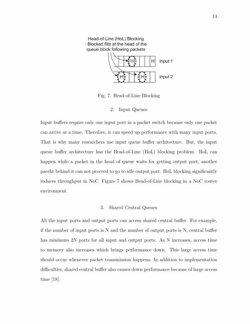
Fig. 7. Head-of-Line Blocking
2. Input Queues
Input buffers require only one input port in a packet switch because only one packet
can arrive at a time. Therefore, it can speed up performance with many input ports.
That is why many researchers use input queue buffer architecture. But, the input
queue buffer architecture has the Head-of-Line (HoL) blocking problem. HoL can
happen while a packet in the head of queue waits for getting output port, another
pacekt behind it can not proceed to go to idle output port. HoL blocking significantly
reduces throughput in NoC. Figure 7 shows Head-of-Line blocking in a NoC router
environment.
3. Shared Central Queues
All the input ports and output ports can access shared central buffer. For example,
if the number of input ports is N and the number of output ports is N, central buffer
has minimum 2N ports for all input and output ports. As N increases, access time
to memory also increases which brings performance down. This large access time
should occur whenever packet transmission happens. In addition to implementation
difficulties, shared central buffer also causes down performance because of large access
time [18].
Page 28
15
crossbarInput ports
(A) FIFO Buffers
output ports
N N/44x1
4x1
4x14x1
output ports
Input
ports
(B) SAFC (Statically
Allocated Fully Connected)
N/4
Input
ports
(C) SAMQ (Statically
Allocated Multi-Queue)
crossbar
output ports
crossbar
Input
ports
output ports
(D) DAMQ (Dynamically
Allocated Multi-Queue)
N
Fig. 8. Alternative Designs of Switching with Input Port Buffers
Page 29
16
C. Diverse Input Port Buffers
1. Single Input Queues
Figure 8 (A) shows that each input port has a single FIFO buffer and each FIFO
buffer receives packets from a previous node. The packets stored are waiting for their
order. In the figure 8 (A), crossbar switch has 4 input and output ports [18].
2. SAFC (Statically Allocated Fully Connected)
Each input port has separate FIFO queue for every output port in order to remove
the Head-of-Line (HoL) blocking problem. If packets arrive at a corresponding queue,
the packets are competing for the same output and thus the packet at the head of
line cannot block other packets. Throughput in SAFC is higher than in single input
queue since each input can transmit N packets every time. However, this SAFC has
several drawbacks. The first one is inefficient buffer utilization because N buffers are
divided by four statically allocated queues, and thus, available buffer space for each
input port is only one quarter of the buffer space. Therefore, it is mandatory to route
all packets in advance to know the destination output port. The second disadvantage
is design complexity. It is required to manage separate buffers and crossbars [18].
3. SAFQ (Statically Allocated Multi-Queue)
In SAMQ, this resolves the second disadvantage of SAFC which is a design complexity.
If packets arrive at buffers, one of the packets is forwarded to the crossbar. Therefore,
it does not need to manage N crossbars. However, SAMQ still has inefficient buffer
utilization [18]. Figure 8 (C) shows SAMQ design.
Page 30
17
Flit k
Flit 3
Flit 2
Flit 1
Flit k
Flit 3
Flit 2
Flit 1
Flit k
Flit 3
Flit 2
Flit 1
Write
Pointer
Read
Pointer
Fig. 9. Generic NoC Router Architecture
4. SAFQ (Statically Allocated Multi-Queue)
In DAMQ scheme, each input buffer uses a single buffer space. In order to increase
buffer utilization, each queue in each input port is dynamically allocated, and this
queue is maintained by a linked list. The dynamic buffer allocation significantly
increase buffer usage. The control logic is composed of head and tail pointers. When-
ever a packet arrives, the packet is stored in the location which the head pointer
directs. While a packet is stored into free buffer space, its destination output port
number will be decided. The tail pointer is responsible for pointing out location to
be sent into crossbars.
Page 31
18
D. Generic NoC Router
Generally, a NoC router has five input and output ports, each of which is for local
processing element (PE) and four directions: North, South, West, and East. Each
router also has five components: Routing Computation (RC) Unit, Virtual Channel
Allocator (VA), Switch Allocator (SA), Flit Buffers (BUF), and Crossbar as we can
see in Figure 9. When the header flit arrives at the internal flit buffer, the RC unit
sends incoming flits to one of physical channels. The Virtual Channel Allocation
unit receives the credit information from the neighboring routers, arbitrates all the
header flits which access the same VCs, and then select one of them according to the
arbitration policy. Therefore, this header flit can set up the path where the following
data and tail flits can traverse this route successfully. The transmitting router sends
the control information to the receiving router, and receiving router may update VC
ID at the internal buffer with this control information. Switch Allocation (SA) unit
arbitrates the waiting flit in all VCs accessing the crossbar and allow only one flit to
get crossbar permission. The SA operation is based on the VA stage since the flit
data in the buffer comes from the previous router in the route. The flit data pass
over the crossbar and thus can arrive at the destination node.
E. Dynamic Virtual Channel Regulator(ViChaR)
1. ViChaR Configuration
The ViChaR is composed of two main components which are the Unified Buffer
Structure (UBS) to share the internal flit buffers with all VCs simultaneously, and
the Unified Control Logic (UCL,) to control UBS and assign buffers into VCs dy-
namically according to the network traffic. UCL has the following 5 logic blocks per
port. Arriving/Departing flit pointers manage the control logic for vk flit buffers
Page 32
19
Fig. 10. Buffer Architecture and Allocation
Page 33
20
where v is the number of VC per port and k is the number of flit buffers per VC.
In Figure 10, we can compare ViChaR router buffer architecture with generic router
buffer architecture. Incoming flits of each packet in the UBS of ViChaR may not
be contiguous. The Slot Availability Tracker provides the next available flit buffer
location depending on the network condition. This allows the router to use a vari-
able number of in-flight packets per port according to the traffic. VC Control Table
remembers all in-use VCs and a detailed flit buffer location per VC in UBS. Each
output port has its own Virtual Control Table to control data flow. VC Availability
Tracker keeps track of the status of available VCs, and Token Dispenser uses the data
that VC Availability Tracker provides.
2. Virtual Channel Allocator and a Switch Allocator
Figure 11 shows a Virtual Channel Allocator and a Switch Allocator in Generic
and ViChaR architecture. A generic router can support only a fixed and statically
assigned number of VCs per input port. On the other hand, ViChaR can provide
a variable number of VCs depending on network traffic. Each input port can have
maximum vk VCs in order to increase buffer utilization in the ViChaR architecture,
and Virtual Control Table keeps track of these buffer locations. It is important to
look at each VA and SA arbiter component. Each vk:1 VA 1st arbiter in the ViChaR
could have longer delay than a v:1 VA 1st arbiter of generic router. In ViChaR [9],
they analyzed the area and power overhead of the ViChaR which are implemented in
structural Register-Transfer Level (RTL) Verilog and then synthesized in Synopsys
Design Compiler using a TSMC 90nm standard cell library.
Page 34
21
Fig. 11. Virtual Channel Allocation and Switch Allocation
Page 35
22
3. Register-Based Buffering
The flit buffers can be implemented in diverse ways. The Memory cell-based buffering
method using a SDRAM type memory cell has latency penalties, and this penalty
happen whenever the flits arrive at and depart from the buffers. ViChaR uses registers
(D-Latch) for buffering, and these D-Latches have only a few delay of control logic. We
implement flit buffers using register based buffering in the same method as ViChaR.
Page 36
23
CHAPTER IV
DESIGN FLOW
This chapter gets through design flow for implementation of virtual channels in a
network-on-chip router. Design flows are the straightforward combination of elec-
tronic design automation tools to accomplish the design of an integrated circuit. In
NoC design, design parameters are topologies, switching techniques, routing protocol,
and flow control mechanisms that we see in the previous chapter. These parameters
are modeled by Verilog-HDL (Hardware Description Language) and then synthesized
by Design Compiler to get gate level netlist. Gate level simulations is performed to
verify functionality and know gate delay.
A. Standard Cell Design
1. Design Library
Virtual channels in a network-on-Chip router are implemented by a generic standard
cell library. The library used is TSMC (Taiwan Semiconductor Manufacturing Com-
pany) 180nm technology. This synopsys design library includes timing specifications
for different operating conditions. The timing specification used is typical case ver-
sion (1.8V). The reason for choosing TSMC 180nm technology is that this library is
available in the Computer Science Department.
2. Hardware Description Language
Verilog (Hardware Description Language) is used to implement virtual channels in a
NoC router. This language supports the design, verification, and implementation of
analog, digital, and mixed-signal circuits at various levels of abstraction.
Page 37
24
Fig. 12. Basic Synthesis Flow with Design Compiler
B. Synthesis with Synopsys Design Compiler
A synthesis tool, Synopsys Design Compiler, takes an RTL hardware description, a
standard cell library, design constraints such as setup and hold time as inputs, and
produces a gate-level netlist which is a list of circuit elements and their interconnec-
tions, area (Gate Count), power consumption, timing information as outputs. The
resulting gate-level netlist is a completely structural description with standard cells.
Figure 12 shows typical synthesis flow with Design Compiler [19].
Page 38
25
C. Design Evaluation Techniques
1. Throughput and Latency
Throughput can be computed as the number of successful flits over a link or a single
physical or logical channel at a maximum speed. Latency is a time delay between a
flit start to be injected at the sending node, and this flit arrives at the target node.
These two factors are affected by congestion where many virtual channels are willing
to send flits simultaneously. In order to measure critical path delay, STA (Static
Timing Analysis) is executed.
2. Area Estimation
Through a Network-on-chip (NoC) router implementation, area information can be
extracted using ”report area” command. Gate count is independent of specific tech-
nology. Therefore, the gate count is measured by Design Compiler command.
3. Power Consumption Measurement
Dynamic power consumption is mainly dependent on switching activity in asyn-
chronous logic. On the other hand, leakage power consumption is proportional to
the area. Design Compiler has a ”report power” command which calculates dynamic
and leakage power on the basis of capacitance and estimated circuit activities.
Page 39
26
CHAPTER V
ROUTER IMPLEMENTATION
A. Asynchronous Design
A Network-on-Chip router is implemented by asynchronous design methodologies
which use implicit or explicit data valid signal instead of clock signals. Asynchronous
design has the following benefits [20]:
1. No Clock Skew
The first advantage is that asynchronous logic has no clock skew. Clock skew is
a phenomenon in synchronous circuits in which the clock signal arrives at different
components at different times. Therefore, asynchronous logic does not have to worry
about clock skew because it has no globally distributed clock.
2. Low Power Consumption
The second advantage is low power consumption. Asynchronous logic only execute in
its own operation while synchronous circuits have to be toggled by clock signal every
time which causes dynamic power consumption.
3. Low Global Wire Delay
A clock cycle of synchronous circuits depends on critical path delay. Hence, setup and
hold timing issue should be carefully controlled and the logic which has critical path
delay must be optimized considering the highest clock rate. However, the performance
of asynchronous circuits can be calculated by the speed of the circuit path currently
in operation.
Page 40
27
4. Automatic Adaptation to Variation
Combinational logic delay can be changed depending on variation such as fabrication,
temperature, and power-supply voltage. A clock cycle should be calculated consider-
ing the worst case variation, for example, low voltage and high temperature. However,
the delay of asynchronous circuits is computed by current physical properties
B. An Arbiter Design
Many input ports which are requestor want to access a common physical channel
resource. In this case, an arbiter is required to determine how the physical channel
can be shared amongst many requestors. When we think about arbitration logic, we
have to consider many factors.
1. Basic Concept of Arbitration
If many flits arrive at buffers from several virtual channels and these flits are destined
for one physical channel, an arbiter receives request signals from buffer such as FIFO
empty or full signals. These FIFO empty and full signals are generated by comparing
write pointers and read pointers. For example, if a write pointer has the same value
as a read pointer, FIFO empty signal will be generated. On the other hand, if a write
pointer has more value than a read pointers, FIFO full signal will be made. Figure
14 shows general arbitration flow in FIFO (First In First Out) based request and a
grant system. When a new flit arrives at FIFO, a write pointer gets incremented and
request signal is generated. An arbiter receive N request signals and grant only one
buffer, and this grant signal increases a read pointer of corresponding FIFO. This
type of arbitration flow is used to implement a NoC router VA and SA logic. Fairness
is a key property of an arbiter. In other words, a fair arbiter support equal service
Page 41
28
Fig. 13. Example of Arbitration in FIFO
to the different requests. In FIFO environment, requesters are served in the order
they made their requests. Even though an arbiter is fair, if traffic congestion is not
fair in a NoC environment, the system cannot be fair. Figure 13 shows a example of
arbitration in FIFO.
2. Fixed Priority Arbiter
One general arbitration scheme is a fixed priority arbiter. Each input port has its own
fixed priority level, and an arbiter grants an active request signal with the highest
priority depending on this priority level. For instance, if request[0] has the highest
priority among N requests, and request[0] is active, it will be granted regardless other
request signals. If request[0] is not active, the request signal with the next highest
priority will be granted. In other words, the current request (lower priority) only
will be served if the previous request (higher priority) has not appeared or been
served already. Therefore, fixed priority arbiter can be used where there are a few
requesters. The implementation of fixed priority arbiter can be done by the following
case statement [21].
Page 42
29
case (request[4:0])
5’b????1 : grant <= 5’b00001;
5’b???10 : grant <= 5’b00010;
5’b??100 : grant <= 5’b00100;
5’b?1000 : grant <= 5’b01000;
5’b10000 : grant <= 5’b10000;
5’b00000 : grant <= 5’b00000;
endcase
Fig. 14. Example of a Fixed Priority Arbiter Code
3. Round-Robin Arbiter
When we use a fixed priority arbiter in NoC design, there is no limit to how long a
lower priority request should wait until it receives a grant. In a round-robin arbiter,
every requester can take a turn in order because a request that was just served should
have the lowest priority on the next round of arbitration. A pointer register maintains
which request is the next one. Hence, a round-robin arbiter is a strong fairness arbiter
[21]. Figure 14 shows a example of a fixed priority arbiter code. In general, a round-
robin arbiter can use N fixed priority arbiter logic. Figure 15 shows a muxed parallel
priority arbiter. The parallel priority arbiter uses N fixed priority arbiters in parallel
for N requesters. Shift module shifts request to the right by t values before arbitration.
Therefore, multiplexer receives all possible grant signals for round-robin arbiter. At
this time, pointer should select which of the intermediate grant vectors will actually
be used. This design is fast, but the area of this design is too much because of N shift
module and fixed priority arbiters with a large number of requesters.
For good area and timing aspect, two fixed priority arbiters with a mask can be
used. In Figure 16, the lower arbiter receives all request signal and the upper arbiter
first masks all request signal before one request signal is selected by the round-robin
Page 43
30
Fig. 15. Muxed Parallel Arbiter
Fig. 16. Two Fixed Priority Arbiters with a Mask
pointer. If upper arbiter selects a grant signal, the grant signal is chosen by MUX
[21].
4. Matrix Arbiter
Matrix arbiter uses a least recently served priority scheme by maintaining a triangle
array of state bit Wij for all i < j. Wij (row i and column j) indicates that request
i takes priority over request j. Only the upper triangular portion of the matrix need
be maintained. Figure 17 shows how a single grant output is generated for a 4-input
arbiter in matrix arbitration. This arbiter ensures that a grant is generated only
Page 44
31
Fig. 17. Matrix Arbiter
Fig. 18. Tree Arbiter
if an input request with a higher priority is not asserted. The flip-flop matrix is
updated after each clock cycle to reflect the new request priorities [22]. This matrix
arbiter is a favorite arbiter for small number of inputs because it is fast, inexpensive
to implement, and provides strong fairness.
5. Tree Arbiter
With a large number of inputs, a tree arbiter organizes these inputs as a tree of smaller
arbiters. Each arbiter eagerly sends request to the upper tree before it determines
which input they will actually grant [22]. The example of tree arbiter is shown in
Figure 18.
Page 45
32
C. A Generic Router
1. High-level View
Figure 19 shows the top view of a generic router. In an implementation, the number
of input and output ports are 5, and each input port has 4 virtual channels. The
inputs are composed of 128 bits incoming flit data per input port, 4-bits data enable
signal per input port, 4-bits virtual channel status per input port, and four virtual
channel requests per input port. The outputs are composed of 128-bits outgoing flit
data per output port, 4-bits output data enable signal per output port, 4-bits current
node virtual channel status signals, and 20-bits virtual channel request signals. There
are VA (Virtual Allocator) , SA (Switch Allocator), and Flit buffers (Flitbuffer p1,
Flitbuffer p2, Flitbuffer p3, Flitbuffer p4, Flitbuffer p5). Each flit buffer is composed
of 16 buffers (4 virtual channels), and each buffer can store a 128-bits flit. A 4-
bits WE (Write Enable) signal (WE p1, WE p2, WE p3, WE p4, WE p5) comes
from each previous node and each bit indicates a WE signal for each virtual channel.
For Virtual-Channel Allocator (VA), current node receives 4-bits VC status from
each neighboring router. These bits indicate how many available virtual channels a
neighboring router has. VA top module also receives total 20 request signals from
adjacent nodes. Each neighboring node send 4 virtual channel request signals in
order to get permission to access available buffers. Each head flit has the direction
information for the following flits. Therefore, flit buffer logic can know direction
of each packet and provides this direction information into VA top module. When
virtual channel arbitration is done, VA top module sends request output signals to
5 neighboring nodes including PE (Processing Element). The details is explained in
the following section. For a Switch Allocator (SA), as soon as a current node gets the
permission of next router’s virtual channel priority and next body flits arrive at flit
Page 46
33
buffers, SA top module receives request signals from buffer module as input signals.
Therefore, if many body flits arrive at buffers, SA top module will receive many input
signal as logic level high. After switch allocation, RE (Read Enable) signal will be
generated. Each bit in a 4-bits RE signal indicates that corresponding flit will be
transferred into appropriate granted virtual channel.
2. Buffer Architecture
Buffer architecture for generic router is given in Figure 20. Flits arrive at flit buffers
with their enable signal (WE). Write pointers with WE signal decide the location
to store flits. 16-flits buffers are divided by 4 parts and each part is for each input
port and each buffer is corresponding to each virtual channel. The basic enable logic
for D-latch is shown in Figure 21. D-latch is used to use advantage of asynchronous
logic. All flit buffers are consisted of these D-latchs. In read operation, a RE (Read
Enable) signal is generated from the Switch Allocator (SW). According to RE and
read pointers, flit buffers send a flit into a crossbar module.
A packet is segmented into flits and then this packet can be delivered with this
segmentation. As we examine packet types in the previous chapter, a packet is consist
of a head flit, body flits, and a tail flit. When a head flit arrive at current node, the
routing logic decides the routing path for the following flits. With the decision of
the routing path, an output physical channel is also determined. In a generic buffer
architecture, each flit buffer can decode and recognize routing information in a head
flit. Each head flit has only one of five directions in the routing path: North, South,
West, East, or Local.
Page 47
34
Fig. 19. Top View of a Generic Router
Page 48
35
Flit_0
Flit_1
Flit_2
Flit_3
Flit_4
Flit_5
Flit_6
Flit_7
Control Logic(Read/Write Pointer)
Flit_8
Flit_9
Flit_10
Flit_11
Control Logic
(Read/Write Pointer)
Flit_12
Flit_13
Flit_14
Flit_15
Control Logic(Read/Write Pointer)
Input port1 To Crossbar
VC ID SA CTL
Control Logic
(Read/Write Pointer)
VC1_empty_p1
VC1_full_p1
VC2_empty_p1
VC2_full_p1
VC3_empty_p1
VC3_full_p1
VC4_empty_p1
VC4_full_p1
Generic Buffer Architecture
Fig. 20. Buffer Architecture of a Generic Router
Page 49
36
Fig. 21. 1-bit D-Latch and Enable Signals
3. Virtual Channel Allocator(VA)
In a router, many input ports, which are requestor, will access a common physical
channel resource. In this case, an arbiter is required to determine how the phys-
ical channel can be shared amongst many requestors. A virtual channel allocator
is composed of two stages in Figure 22. The first stage of VA receives neighboring
router’s virtual channel status and previous router’s request signals. A direction of
a head flit is used to match VC status with VC requests. The purpose of 2nd stage
is to generate virtual channel request signals with an available virtual channel of the
next router. The two fixed priority arbiter with a mask is used to implement virtual
channel arbitration logic. The basic architecture of a virtual channel block is based
on [22]. In the first stage of VA, a 4:1 arbiter reduces the number of requests from
each input VC to one output VC. Therefore, total 20 4:1 arbiters are used in the first
stage of VA. The second stage of VA selects one from the maximum 20 requests to
use one output VC, and thus total 20 20:1 arbiters are used in the second stage of
VA.
4. Switch Allocator(SA)
Once a path is set as a routing path, a virtual channel in both input and output
port is dedicated for an entire routing path. Other flits will use the remaining VCs
in a generic router. Therefore, each packet has its own a virtual channel. Then, a
Page 50
37
Fig. 22. Virtual Channel Allocator in a Generic Router
Page 51
38
switch allocator will grant the following flits when they arrive at flit buffers. If there
are multiple requests, a SA will select the winner in a round-robin fashion for each
priority level. Figure 23 (a) shows switch allocator block diagram. In the first stage
of SA, each input port has v virtual channels. It means that v input channels are
sharing one crossbar port. Thus, 1st stage switch allocator selects one request from
the input VC. In the second stage of SA, each p:1 arbiter arbitrates between winning
requests from each input port, total p input ports, for output ports. Therefore, total
P v:1 arbiters are required in the first stage and P p:1 arbiter is needed for the second
stage of SA. In a router implementation, the number of virtual channel are 4 and the
number of ports are 5. Figure 23 (b) shows detail implementations. The inputs of 1st
stage of SA are data enable signals per virtual channel. For example, sa input1 v1
is coming from virtual channel 1 data enable from the north side. Therefore, there
are total 20 inputs in the 1st stage switch allocator. The output signals of 4:1 arbiter
in the 1st stage SA is a winning flit which selects the inputs of the 2nd stage SA.
P1 vc0 en signal has 5-bits width and is coming from the direction information of a
incoming flit. Hence, a incoming flit can generate a input signal for 2nd stage of SA
with direction information. With the same method, a 2nd stage arbiter will arbitrate
and select a candidate flit and thus can generate a RE (Read Enable) signal for buffers.
In the 2nd stage, the winning flit is ORing and generates the SUCCESS signal for the
1st stage arbiter. The 1st stage arbiter receives the SUCCESS signal since this arbiter
should know whether its winning flit has permission to access crossbar or not. If a
winning flit can be forwarded to crossbar, 1st stage arbiter can go further to arbitrate
next flits. Otherwise, 1st stage arbiter would continue to generate the same signal
again. During these processes, flits in a buffer have to wait for getting admission of
the crossbar. Throughput and latency can be determined by the delay of a virtual
channel allocator and switch allocator. Therefore, we need to analyze critical path
Page 52
39
delay in these blocks.
5. Crossbar Switch and Other Implementation
The crossbar fabric module in the design is responsible for physically connecting an
input port to its destined output port, based on the grant issued by the scheduler.
In every crossbar, the cross-points are controlled by the CNTRL input of the mod-
ule. If a certain CNTRL bit is high, then the corresponding cross point is closed.
Figure 24 shows crossbar fabric implementation in a NoC router. 5-bits control sig-
nal(direction p1, direction p2, direction p3, direction p4, direction p5) is determined
by output signals of 2nd stage SA. This control signals are used by a crossbar to decide
which input ports have to be connected into output ports. According to the control
signals, a whole connection between source and target nodes is accomplished. RC
(Route Computation) logic is not implemented in thesis project since the RC module
is required to implement a whole system and RC module needs routing algorithm in
a NoC router. Therefore, without RC module, we implemented a generic router using
Verilog.
D. A Virtual Channel Regulator
1. High-level View
Figure 25 shows the top view of the virtual channel regulator (ViChaR) buffer archi-
tecture. The implementation environment is different from a generic router. Each a
number of input ports and output ports is 5. But there is no fixed virtual channel
since ViChaR distributes virtual channels according to network traffic. ViChaR uses
a Unified Buffer Structure (UBS) instead of individual FIFO buffers [9]. This UBS
allows a router to use a dynamically assigned virtual channel management scheme.
Page 53
40
Fig. 23. Switch Allocator in a Generic Router
Page 54
41
Fig. 24. Crossbar Switch in a Generic Router
Page 55
42
The main difference between a generic and ViChaR router is that ViChaR uses a
novel, tabled-based design which provides single-clock operation without overhead.
In the Figure 25, VC Control Table receives many control information such as the
number of available flit buffers, the number of available virtual channels, and the
direction information of flit packets. The ViChaR is controlled by Unified Control
Logic (UCL). UCL is composed of five parts: Arriving/Departing Flit Pointers Logic,
Slot Availability Tracker, VC Availability Tracker, VC Control Table, and Token Dis-
penser. The VC and Slot Availability Tracker is looking at all VCs in VC Control
Table and thus informs the available VCs and slots of Token Dispenser in order to
assign VCs to incoming flits, and a new flit is stored in the location which the Slot
Available Tracker points out. These two blocks are located at each flit buffer module.
The VC Control Table is shown in Figure 25. This VC Control Table contains slot
IDs of all flits currently and VC IDs in the buffers. The current location of a head
flit, data flits, and a tail flit are indicated by the VC Control Table. This location
information increases buffer utilization because of flexibility, and this removes disad-
vantages caused by statically-allocated buffer architecture. In addition, it is possible
to manage a variable number of VCs using VC Control Table. The Token dispenser
is responsible for dispensing free VCs to requesting flits. A Virtual channel Allocator
(VA) receives slot status bits and each request from the previous routers as input sig-
nals. Switch Allocator (SA) also receives available slot information from VC Control
Table as input signals. The crossbar fabric module is the same as a generic router.
2. Buffer Architecture
Buffer architecture for ViChaR is shown in Figure 26. The difference between a
generic router and ViChaR buffer architecture is that ViChaR is composed of unified
buffer structure which is controlled by unified control logic (UCL). Each input port has
Page 56
43
Fig. 25. Top View of a ViChaR
Page 57
44
Fig. 26. Unified Buffer Structure(UBS) in a ViChaR
one UBS and UCL. In a heavy traffic, increasing the number of VCs is a more effective
way of improving performance than increasing buffer depth since many packets are
contending for routing resource. On the other hand, in light traffic, increasing buffer
depth is more efficient way than increasing the number of VCs. Therefore, it is
required to dynamically allocate buffer resource into VCs according to traffic. Figure
27 shows these limitations of statically allocated buffer architecture.
Page 58
45
T D D H VC0
T D D H VC1
Two packets
blocked due to
shallow VCs
VC v
Remaining
buffer slots are
not utilized
(a) Light Traffic
Many/Shallow VCs
T D D H VC0
T D D H VC1
H VC v
(b) Heavy Traffic
Many/Shallow VCs
Inefficient Efficient
T D D
Buffer slots are
fully utilized
T D D H VC0
VC1
Both packets
accommodate
d by deep VCs
(c) Light Traffic
Few/Deep VCs
efficient
T D D H
Buffer slots are
fully utilized
T D D H VC0
VC1T D D H
Two packets
accommodate
d by deep VCs
T D D H
T D D H
Remaining
packets
blocked due
to lack of VCs
(d) Heavy Traffic
Few/Deep VCs
Inefficient
Fig. 27. Limitation of a Statically Assigned Buffer Organization
Page 59
46
3. Virtual Channel Allocator(VA)
A Unified Buffer Structure (UBS) does not have a fixed number of buffering space.
For one packet, vk buffer spaces per port are dynamically allocated according to the
traffic condition. In 1st stage of VA, virtual channel allocator receives neighboring
router’s slot status and previous router’s request signals. Therefore, total P*P vk:1
arbiters in the 1st stage VA and P P:1 arbiters in the 2nd stage VA are used to set up
the routing path. The two fixed priority arbiters with a mask are used to implement
arbitration logic. The difference between a generic router VA and ViChaR VA is
that ViChaR has much more the number of inputs than a generic router in the 1st
stage VA. However, a ViChaR router has fewer the number of inputs than a generic
router in the 2nd stage VA. Therefore, during implementation, we compared area,
power consumption, and latency of these two virtual channels. Figure 28 shows VA
implementation details in a ViChaR.
4. Switch Allocator(SA)
A Switch Allocator (SA) of ViChaR is different from that of a generic router. Once
a path is set as a routing path, a switch allocator grants the following data flits
and a tail flit. Whenever a head flit sets up the routing path and the amount of
flits, the allocated number of flits will be different according to the amount of traffic.
VC Control table provides these information about the amount of the available flits
in the buffers. In the first stage of SA, 16-bits slot availability and data enable
signal are ANDing to generate valid data signals among these inputs. These inputs
go to the input of the 1st stage SA. The first stage arbiter selects a winner, and
the winner goes to the input of the 2nd stage SA with direction information. The
second stage of SA arbitrates the inputs which access to the same direction. In order
Page 60
47
Fig. 28. Virtual Channel Allocator in a ViChaR
Page 61
48
Fig. 29. VC/Slot Availability Tracker
to measure performance, we compared the area, power consumption, timing of SA
module between a generic and ViChaR router. Figure 30 shows SA implementation
details in a ViChaR.
5. VC/Slot Availability Tracker
A VC and Slot Availability Tracker keep track of all the VCs and slots in the VC
Control Table. Based on available VC and Slot information, new incoming packets
and flits are assigned . In Figure 29, logic high indicates that VC/Slot is avail-
able, and logic low shows that VC/Slot is occupied. Both trackers have a pointer
to point out the available entry. If all VCs and Slot are used by the packets and
flits, adjacent router will not send packets and flits any more. VC/Slot Availability
Tracker is implemented by comparing write pointer and read pointer. If the value of
both pointer is the same, VC/Slot Availability value indicate logic ’1’ which means
VC/Slot Availability in each ID has a available space to store packets and flits.
6. VC Control Table
A VC Control Table is composed of Slot IDs of all flits in the buffers. Each VC ID
has space to store a entire packet: a head flit, data flits, and a tail flit. From Figure
Page 62
49
Fig. 30. Switch Allocator in a ViChaR
Page 63
50
Fig. 31. VC Control Table
31, VC 0 has a head flit in slot 0, two data flits in slot 1 and 3, and a tail flit in slot
5. This scheme increases buffer utilization since the buffer space can be dynamically
assigned according to the number of packets. For example, if 10 packets are coming
from east direction, VC Control Table will assign 10 VC rooms for the packets. VC
Control Table receives VC/slot availability signals from buffer module in order to
build tables and then generate slot availability signal for Switch Allocator module.
Also it send slot status signals for neighboring routers.
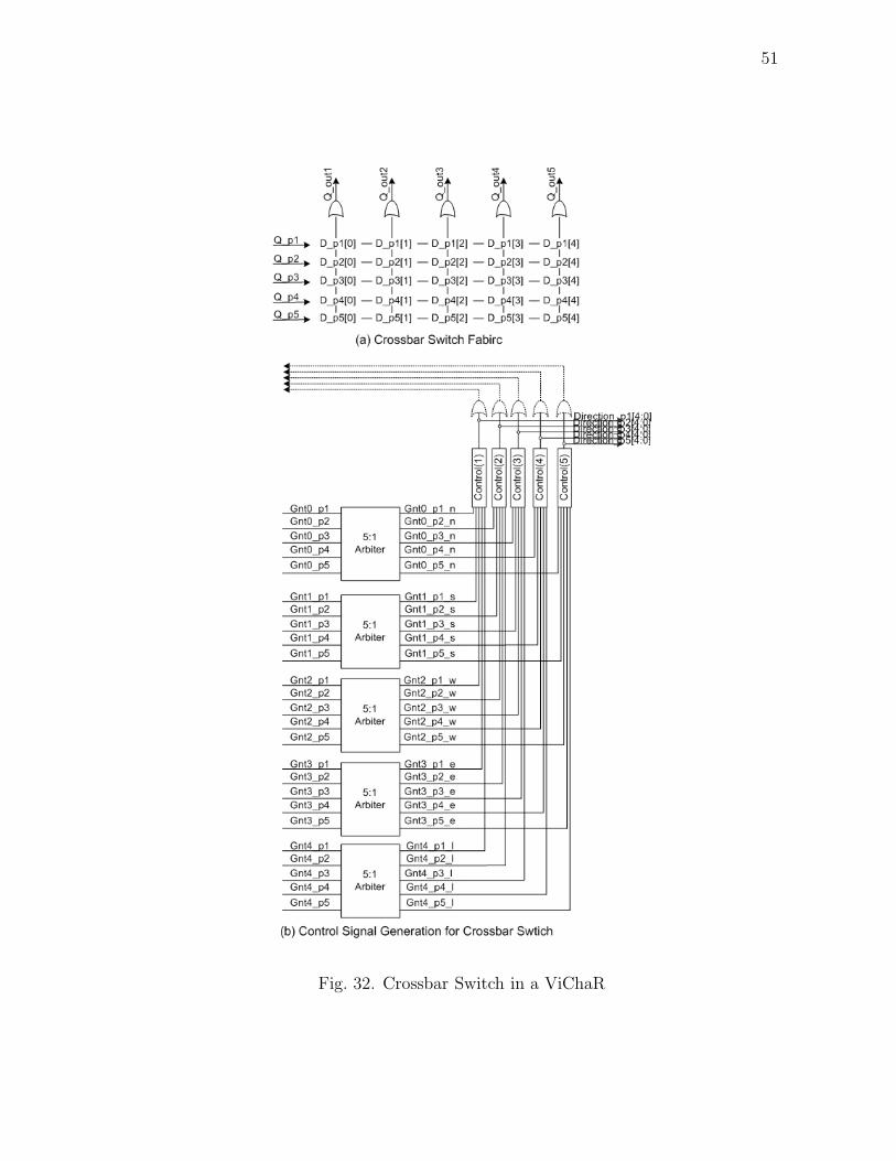
7. Crossbar Switch in a ViChaR
The crossbar fabric module in a ViChaR router is responsible for physically connect-
ing an input port to its destined output port based on the control signal from SA.
If a certain CNTRL bit is high, then the corresponding cross point is closed. 5-bits
control signals(direction p1, direction p2, direction p3, direction p4, direction p5) is
determined by output signals of 2nd stage SA. This control signals are used by cross-
bar to decide which input ports have to be connected into output ports. According
to the control signals, a whole connection between source and target nodes is accom-
plished. Figure 32 shows crossbar implementation details in a ViChaR.
Page 64
51
Fig. 32. Crossbar Switch in a ViChaR
Page 65
52
CHAPTER VI
RESULT AND OTHER DISCUSSION
This chapter presents performance and cost measurement for a generic router and
ViChaR implementations presented in previous chapter. In order to analyze area,
power consumption and performance, these two router architectures are implemented
in structural Register-Transfer Level (RTL) Verilog and then synthesized in a Syn-
opsys Design Compiler using TSMC 180nm standard cell library. We set up the
synthesis environment using an operating voltage of 1.8V (typical voltage) and a
clock frequency of 100MHz. The router has 5 input and output ports, 4 VCs per
input port, 4 flits per VC, and 128 bits per flit. The area, power consumption, and
critical path delay is extracted from synthesized results.
A. Area Estimation
We estimated area of a generic and a ViChaR router, and investigate how it is affected
by implementing dynamically allocated buffer architecture in a ViChaR. The area
consumed by a router is divided by cell area and interconnect area.
1. Cell Area
The Cell area is composed of combinational and non-combinational area, and the
number of gate count can be calculated by the Gate Count formula. The total cell
area of a generic router and a ViChaR are shown in Table I and Figure 33. In total
cell area estimation, VA of a generic router has much more area than VA of a ViChaR
since the 2nd stage arbiters in a generic router has more the number of inputs than
that of a ViChaR. In arbitration logic, as the number of input increases, the area also
increase. On the other hand, SA of a ViChaR has more area than SA of a generic
Page 66
53
Table I. Total Cell Area (TSMC 180nm), G:Generic, V:ViChaR
Total Cell Area VA G VA V SA G SA V Buffer G Buffer V Total G Total V
Combinational Area 11196 9443 1465 3492 35197 31425 47858 46251
Non-Combin. Area 7040 6233 66 1540 11146 10560 18252 18333
Total Cell Area 18236 15567 1531 5032 46343 41985 66110 64584
Percentage 27.5% 24.9% 2.3% 8% 70.2% 67.1% 100% 100%
Table II. Net Interconnect Area (TSMC 180nm), G:Generic, V:ViChaR
Interconnect Area VA G VA V SA G SA V Buffer G Buffer V Total G Total V
Net Intercon. Area 145 77 14 32 696 696 855 805
Percentage 16.9% 9.5% 1.6% 3.9% 81.5% 86.6% 100% 100%
router because the 1st stage arbiters in a ViChaR has much more input signals than
a generic router. The buffer area of a ViChaR is almost the same as that of a generic
router.
2. Interconnect and Total Area
Table II and Figure 34 show net interconnect area. Interconnect area has similar
tendency with total cell area. The interconnect area of a VA module in a generic
router is greater than that of ViChaR. On the other hand, the interconnect area of a
SA module in a ViChaR is greater than a generic router. Therefore, Total area has
Table III. Total Area (TSMC 180nm), G:Generic, V:ViChaR
Total Area VA G VA V SA G SA V Buffer G Buffer V Total G Total V
Total Area 18381 15644 1545 5064 47039 47681 66965 65389
Percentage 27.4% 24.7% 2.3% 8% 70.2% 67.3% 100% 100%
Page 67
54
0
10000
20000
30000
40000
50000
60000
70000
Generic ViChaR Generic ViChaR Generic ViChaR Generic ViChaR
VA SA Buffer Total
Ga
te
Co
un
t
Axis Title
Total Cell Area
Combin. Area
Non-Combin. Area
Total Cell Area
Fig. 33. Total Cell Area Comparison (TSMC 180nm)
0
100
200
300
400
500
600
700
800
900
Generic ViChaR Generic ViChaR Generic ViChaR Generic ViChaR
VA SA Buffer Total
Ga
te
Co
un
t
Net Intercon. Area
Fig. 34. Net Interconnect Area Comparison (TSMC 180nm)
also the same trend as total cell area and net interconnect area. The total area of a
generic router and a ViChaR are shown in Table III and Figure 35.
B. Power Consumption Estimation
Power consumption is another important parameter in a NoC router design. First,
we look into dynamic power consumption which is determined by switching activity,
and then we will consider leakage power consumption.
Page 68
55
0
10000
20000
30000
40000
50000
60000
70000
Ge
ne
ric
ViC
ha
R
Ge
ne
ric
ViC
ha
R
Ge
ne
ric
ViC
ha
R
Ge
ne
ric
ViC
ha
R
VA SA Buffer Total
Ga
te
Co
un
t
Total Area
Total Area
Fig. 35. Total Area Comparison (TSMC 180nm)
1. Dynamic Power Consumption
Design Compiler reports dynamic power consumption in each module. Cell internal
power consumption is corresponding to dynamic power in the cell when switching
activity happens. Net switching power is the power consumed when switching a net
from one state to another one. From Table IV and Figure 36, we can conclude that dy-
namic power consumption in buffers is dominant in the total power consumption since
D-latch consumes many dynamic power and has many switching activities. In addi-
tion, a virtual channel allocator also consumes similar dynamic power consumption
compared to buffers. This dynamic power consumption depends on Design Compiler
algorithm. Therefore, in order to improve correctness, we dumped switching activ-
ity through dynamic simulation and then import these switching activity into power
calculation.
2. Cell Leakage Power Consumption
From Table V and Figure 37, cell leakage power consumption is proportional to
total area which we look into in the previous section. Therefore, leakage power
Page 69
56
Table IV. Dynamic Power Consumption (TSMC 180nm), G:Generic, V:ViChaR
Dynamic Power VA G VA V SA G SA V Buffer G Buffer V Total G Total V
Cell Internal(mW) 80.46 85.95 13.93 28.72 87.29 155.07 181.68 269.74
Net Switching (mW) 70.53 93.84 12.23 32.21 35.26 68.38 118.03 195.432
Total Dynamic (mW) 151.0 180.8 26.16 60.93 122.55 223.46 299.7 465.17
Table V. Leakage Power Consumption (TSMC 180nm), G:Generic, V:ViChaR
Leakage Power VA G VA V SA G SA V Buffer G Buffer V Total G Total V
Cell Internal(nW) 381.3 328.57 43.67 103.8 1991.2 1980.8 2416.19 2413.21
consumption in buffer module is dominant in the total leakage power consumption.
Future technology will suffer from increased cell-leakage. Therefore, the leakage power
also will become an important part of the a NoC router.
C. Latency Estimation
The latency can be described as the time passing from a source node to a destination
node through intermediate nodes. In this thesis, we measure critical path delay inside
a router. The critical path delay is important factor to decide performance such as
throughput. Critical path delay can be determined by the delay of virtual channel
allocator (VA) and switch allocator (SA). Figure 38 shows the pipeline stages of both
a generic router and the ViChaR router. [16] presents that the critical path is not
changed and the performance is not affected by modifying VA and SA. Through our
implementation, the critical path is not changed, but critical path delay is significantly
affected by modified VA and SA. In order to compute critical path delay, we do Static
Timing Analysis (STA) using Design Compiler. Figure 39 shows the VA delay in a
generic router. The delay of from a vc0 p1 request input signal to 2nd stage VA
Page 70
57
0
50
100
150
200
250
Generic ViChaR Generic ViChaR Generic ViChaR
VA SA Buffer
Po
we
r C
on
sum
pti
on
(mW
)
Dynamic Power Consumption
Cell Internal(mW)
Net Switching(mW)
Total Dynamic(mW)
Fig. 36. Dynamic Power Consumption Comparison (TSMC 180nm)
0200400600800
1000
1200
1400
1600
1800
2000
Generic ViChaR Generic ViChaR Generic ViChaR
VA SA Buffer
nW
Cell Leakage(nW)
Cell Leakage(nW)
Fig. 37. Leakage Power Consumption Comparison (TSMC 180nm)
Page 71
58
Fig. 38. Generic and ViChaR NoC Router Pipeline
output signal is 4.28ns. Figure 40 shows the VA delay in a ViChaR router. The delay
of from p1 request to outp1 en is 4.14ns. The delay(3.06ns) of 1st stage VA arbiter
in a ViChaR is larger than that of 1st stage VA arbiter in a generic router (0.92ns)
because the number of input in a ViChaR router increases. On the other hand, the
delay(1.08ns) of 2nd stage VA arbiter in a ViChaR is smaller than that (3.36ns) of a
2nd stage VA arbiter in a generic router because the number of input in a ViChaR
router increases.
Figure 41 shows the delay of a switch allocator in a generic router, and Figure
42 shows the delay of switch allocator in a ViChaR router. In the SA module timing
analysis, the delay of 2nd stage arbiter between a generic router and a ViChaR router
is almost the same, but the delay of 1st stage arbiter is quite different. The 1st stage
arbiter in a ViChaR router has more inputs than the 1st stage arbiter in a generic
router. Therefore, the delay (0.96ns) of a 1st stage arbiter in a generic router is
shorter than the delay (3.02ns) of a 1st stage arbiter in a ViChaR router. In other
words, this delay will decrease performance of the ViChaR. The delay of 2nd stage
Page 72
59
Startpoint: vc0_p1_request(input port)
Endpoint: arbiter_top/VA_top/VA_2nd_v1_p1/gnt0
(rising edge-triggered flip-flop clocked by clock')
Point Incr Path
----------------------------------------------------------------------------------------------------------
clock (input port clock) (rise edge) 0.00 0.00
input external delay 0.00 0.00 f
vc0_p1_request (in) 0.00 0.00 f
arbiter_top/vc0_p1_request (arbiter_top) 0.00 0.00 f
arbiter_top/VA_top/vc0_p1_request (VA_top) 0.00 0.00 f
arbiter_top/VA_top/U589/Y (OAI21X1) 0.05 0.05 r
arbiter_top/VA_top/U127/Y (INVX2) 0.06 0.11 f
arbiter_top/VA_top/VA_1st_p1_1/req0 (arbiter_21) 0.00 0.11 f
arbiter_top/VA_top/VA_1st_p1_1/U31/Y (INVX2) 0.08 0.19 r
arbiter_top/VA_top/VA_1st_p1_1/U30/Y (OAI22X1) 0.12 0.31 f
arbiter_top/VA_top/VA_1st_p1_1/U25/Y (NOR2X1) 0.20 0.52 r
arbiter_top/VA_top/VA_1st_p1_1/U24/Y (OAI21X1) 0.11 0.62 f
arbiter_top/VA_top/VA_1st_p1_1/U23/Y (INVX2) 0.06 0.68 r
arbiter_top/VA_top/VA_1st_p1_1/gnt0 (arbiter_21) 0.00 0.68 r
arbiter_top/VA_top/U266/Y (INVX2) 0.09 0.77 f
arbiter_top/VA_top/U1063/Y (NOR2X1) 0.16 0.92 r
arbiter_top/VA_top/VA_2nd_v1_p1/req0 (arbiter_20_19) 0.00 0.92 r
arbiter_top/VA_top/VA_2nd_v1_p1/U175/Y (AOI22X1) 0.12 1.05 f
arbiter_top/VA_top/VA_2nd_v1_p1/U174/Y (OAI21X1) 0.12 1.17 r
arbiter_top/VA_top/VA_2nd_v1_p1/U173/Y (INVX2) 0.06 1.23 f
arbiter_top/VA_top/VA_2nd_v1_p1/U172/Y (OAI21X1) 0.12 1.35 r
arbiter_top/VA_top/VA_2nd_v1_p1/U168/Y (NOR2X1) 0.14 1.49 f
arbiter_top/VA_top/VA_2nd_v1_p1/U167/Y (OAI21X1) 0.18 1.67 r
arbiter_top/VA_top/VA_2nd_v1_p1/U162/Y (NOR2X1) 0.15 1.82 f
arbiter_top/VA_top/VA_2nd_v1_p1/U161/Y (OAI21X1) 0.12 1.94 r
arbiter_top/VA_top/VA_2nd_v1_p1/U160/Y (INVX2) 0.06 2.00 f
arbiter_top/VA_top/VA_2nd_v1_p1/U159/Y (OAI21X1) 0.15 2.15 r
arbiter_top/VA_top/VA_2nd_v1_p1/U154/Y (NOR2X1) 0.15 2.30 f
arbiter_top/VA_top/VA_2nd_v1_p1/U153/Y (OAI21X1) 0.09 2.39 r
arbiter_top/VA_top/VA_2nd_v1_p1/U152/Y (INVX2) 0.07 2.46 f
arbiter_top/VA_top/VA_2nd_v1_p1/U151/Y (OAI21X1) 0.13 2.59 r
arbiter_top/VA_top/VA_2nd_v1_p1/U150/Y (INVX2) 0.04 2.63 f
arbiter_top/VA_top/VA_2nd_v1_p1/U148/Y (NAND2X1) 0.13 2.76 r
arbiter_top/VA_top/VA_2nd_v1_p1/U147/Y (AOI21X1) 0.13 2.89 f
arbiter_top/VA_top/VA_2nd_v1_p1/U146/Y (OAI21X1) 0.12 3.01 r
arbiter_top/VA_top/VA_2nd_v1_p1/U145/Y (AOI21X1) 0.11 3.11 f
arbiter_top/VA_top/VA_2nd_v1_p1/U144/Y (INVX2) 0.10 3.22 r
arbiter_top/VA_top/VA_2nd_v1_p1/U139/Y (NOR2X1) 0.77 3.99 f
arbiter_top/VA_top/VA_2nd_v1_p1/U138/Y (OAI21X1) 0.24 4.22 r
arbiter_top/VA_top/VA_2nd_v1_p1/U137/Y (INVX2) 0.05 4.28 f
arbiter_top/VA_top/VA_2nd_v1_p1/gnt0 (arbiter_20_19)
Fig. 39. VA Critical Path Delay in a Generic Router
Page 73
60
Startpoint: p1_request (input port)
Endpoint: output_p1_en (output port)
Path Group: (none)
Path Type: max
Point Incr Path
-----------------------------------------------------------------------------------------------------------------
input external delay 0.00 0.00 r
p1_request (in) 0.00 0.00 r
arbiter_top/p1_request (arbiter_top) 0.00 0.00 r
arbiter_top/VA_top/p1_request (VA_top) 0.00 0.00 r
arbiter_top/VA_top/U81/Y (INVX2) 0.07 0.07 f
arbiter_top/VA_top/U686/Y (BUFX2) 0.19 0.25 f
arbiter_top/VA_top/U352/Y (NOR2X1) 0.17 0.43 r
arbiter_top/VA_top/VA_1st_p1_1/req0 (arbiter_16_1_24) 0.00 0.43 r
arbiter_top/VA_top/VA_1st_p1_1/U139/Y (AOI22X1) 0.12 0.55 f
arbiter_top/VA_top/VA_1st_p1_1/U138/Y (OAI21X1) 0.12 0.67 r
arbiter_top/VA_top/VA_1st_p1_1/U137/Y (INVX2) 0.06 0.73 f
arbiter_top/VA_top/VA_1st_p1_1/U136/Y (OAI21X1) 0.15 0.88 r
arbiter_top/VA_top/VA_1st_p1_1/U131/Y (NOR2X1) 0.15 1.03 f
arbiter_top/VA_top/VA_1st_p1_1/U130/Y (INVX2) 0.10 1.13 r
arbiter_top/VA_top/VA_1st_p1_1/U125/Y (NOR2X1) 0.12 1.25 f
arbiter_top/VA_top/VA_1st_p1_1/U124/Y (OAI21X1) 0.14 1.39 r
arbiter_top/VA_top/VA_1st_p1_1/U123/Y (AOI21X1) 0.11 1.49 f
arbiter_top/VA_top/VA_1st_p1_1/U121/Y (NAND2X1) 0.14 1.64 r
arbiter_top/VA_top/VA_1st_p1_1/U120/Y (AOI21X1) 0.13 1.76 f
arbiter_top/VA_top/VA_1st_p1_1/U119/Y (OAI21X1) 0.12 1.89 r
arbiter_top/VA_top/VA_1st_p1_1/U118/Y (AOI21X1) 0.11 1.99 f
arbiter_top/VA_top/VA_1st_p1_1/U117/Y (INVX2) 0.10 2.09 r
arbiter_top/VA_top/VA_1st_p1_1/U167/Y (OR2X2) 0.19 2.28 r
arbiter_top/VA_top/VA_1st_p1_1/U166/Y (INVX2) 0.37 2.65 f
arbiter_top/VA_top/VA_1st_p1_1/U62/Y (NAND3X1) 0.21 2.86 r
arbiter_top/VA_top/VA_1st_p1_1/U58/Y (INVX2) 0.05 2.91 f
arbiter_top/VA_top/VA_1st_p1_1/U57/Y (AOI22X1) 0.08 2.99 r
arbiter_top/VA_top/VA_1st_p1_1/U56/Y (NOR2X1) 0.07 3.06 f
arbiter_top/VA_top/VA_1st_p1_1/gnt5 (arbiter_16_1_24) 0.00 3.06 f
arbiter_top/VA_top/U666/Y (NOR2X1) 0.07 3.13 r
arbiter_top/VA_top/U662/Y (NAND3X1) 0.05 3.18 f
arbiter_top/VA_top/U112/Y (OR2X2) 0.14 3.33 f
arbiter_top/VA_top/VA_2nd_p1/req0 (arbiter_5_9) 0.00 3.33 f
arbiter_top/VA_top/VA_2nd_p1/U36/Y (AOI22X1) 0.12 3.45 r
arbiter_top/VA_top/VA_2nd_p1/U35/Y (OAI21X1) 0.11 3.56 f
arbiter_top/VA_top/VA_2nd_p1/U34/Y (INVX2) 0.09 3.65 r
arbiter_top/VA_top/VA_2nd_p1/U33/Y (NAND3X1) 0.05 3.70 f
arbiter_top/VA_top/VA_2nd_p1/U32/Y (INVX2) 0.11 3.81 r
arbiter_top/VA_top/VA_2nd_p1/U27/Y (OAI21X1) 0.07 3.88 f
arbiter_top/VA_top/VA_2nd_p1/U26/Y (OAI21X1) 0.06 3.94 r
arbiter_top/VA_top/VA_2nd_p1/U25/Y (AND2X1) 0.08 4.03 r
arbiter_top/VA_top/VA_2nd_p1/gnt1 (arbiter_5_9) 0.00 4.03 r
arbiter_top/VA_top/U366/Y (NOR2X1) 0.07 4.09 f
arbiter_top/VA_top/U365/Y (NAND3X1) 0.04 4.14 r
arbiter_top/VA_top/output_p1_en (VA_top) 0.00 4.14 r
Fig. 40. VA Critical Path Delay in a ViChaR Router
Page 74
61
arbiter in a ViChaR router determines the minimum clock period and affect pipeline
depth or the clock frequency.
Page 75
62
Startpoint: output1_v1_en[0]
Endpoint: dpsram_top/reg_dpsram_port1/RE_edge_reg[0]
Path Group: clock
Path Type: max
Point Incr Path
---------------------------------------------------------------------------------------------------------------------
-
arbiter_top/VA_top/output1_v1_en[0] (VA_top) 0.00 0.00 f
arbiter_top/U237/Y (INVX2) 0.06 0.06 r
arbiter_top/U503/Y (NAND2X1) 0.05 0.11 f
arbiter_top/U502/Y (NOR2X1) 0.06 0.17 r
arbiter_top/U491/Y (NAND3X1) 0.09 0.26 f
arbiter_top/SA_top/sa_input1_v1 (SA_top) 0.00 0.26 f
arbiter_top/SA_top/SA_1st_stage_p1/req0 (arbiter_4_5_4) 0.00 0.26 f
arbiter_top/SA_top/SA_1st_stage_p1/U31/Y (INVX2) 0.09 0.35 r
arbiter_top/SA_top/SA_1st_stage_p1/U30/Y (OAI22X1) 0.13 0.48 f
arbiter_top/SA_top/SA_1st_stage_p1/U25/Y (NOR2X1) 0.20 0.68 r
arbiter_top/SA_top/SA_1st_stage_p1/U22/Y (OAI21X1) 0.07 0.75 f
arbiter_top/SA_top/SA_1st_stage_p1/U21/Y (OAI21X1) 0.07 0.82 r
arbiter_top/SA_top/SA_1st_stage_p1/U20/Y (AND2X1) 0.14 0.96 r
arbiter_top/SA_top/SA_1st_stage_p1/gnt1 (arbiter_4_5_4) 0.00 0.96 r
arbiter_top/SA_top/U260/Y (NOR2X1) 0.07 1.03 f
arbiter_top/SA_top/U259/Y (NAND3X1) 0.11 1.14 r
arbiter_top/SA_top/U258/Y (NOR2X1) 0.12 1.26 f
arbiter_top/SA_top/U71/Y (INVX2) 0.07 1.33 r
arbiter_top/SA_top/U246/Y (NOR2X1) 0.06 1.39 f
arbiter_top/SA_top/U244/Y (AOI22X1) 0.11 1.50 r
arbiter_top/SA_top/U243/Y (NAND3X1) 0.12 1.62 f
arbiter_top/SA_top/SA_2nd_stage_S/req0 (arbiter_5_3) 0.00 1.62 f
arbiter_top/SA_top/SA_2nd_stage_S/U36/Y (AOI22X1) 0.14 1.76 r
arbiter_top/SA_top/SA_2nd_stage_S/U35/Y (OAI21X1) 0.11 1.87 f
arbiter_top/SA_top/SA_2nd_stage_S/U34/Y (INVX2) 0.09 1.96 r
arbiter_top/SA_top/SA_2nd_stage_S/U33/Y (NAND3X1) 0.05 2.01 f
arbiter_top/SA_top/SA_2nd_stage_S/U32/Y (INVX2) 0.11 2.12 r
arbiter_top/SA_top/SA_2nd_stage_S/U31/Y (OAI21X1) 0.09 2.21 f
arbiter_top/SA_top/SA_2nd_stage_S/U30/Y (INVX2) 0.09 2.30 r
arbiter_top/SA_top/SA_2nd_stage_S/gnt0 (arbiter_5_3) 0.00 2.30 r
arbiter_top/SA_top/U296/Y (NOR2X1) 0.07 2.37 f
arbiter_top/SA_top/U295/Y (NAND3X1) 0.13 2.50 r
arbiter_top/SA_top/U294/Y (AND2X1) 0.08 2.58 r
arbiter_top/SA_top/RE_p1[0] (SA_top) 0.00 2.58 r
Fig. 41. SA Critical Path Delay in a Generic Router
Page 76
63
Startpoint: p1_request (input port)
Endpoint: dpsram_top/reg_dpsram_port1/RE_edge_reg[0]
Path Group: clock
Path Type: max
Point Incr Path
----------------------------------------------------------------------------------------------------------------------
clock (input port clock) (rise edge) 0.00 0.00
input external delay 0.00 0.00 r
p1_request (in) 0.00 0.00 r
arbiter_top/p1_request (arbiter_top) 0.00 0.00 r
arbiter_top/SA_top/p1_request (SA_top) 0.00 0.00 r
arbiter_top/SA_top/U682/Y (INVX2) 0.19 0.19 f
arbiter_top/SA_top/U280/Y (NOR2X1) 0.18 0.38 r
arbiter_top/SA_top/SA_1st_stage_p1/req0 (arbiter_16_5_4)
arbiter_top/SA_top/SA_1st_stage_p1/U139/Y (AOI22X1) 0.12 0.50 f
arbiter_top/SA_top/SA_1st_stage_p1/U138/Y (OAI21X1) 0.12 0.62 r
arbiter_top/SA_top/SA_1st_stage_p1/U137/Y (INVX2) 0.06 0.69 f
arbiter_top/SA_top/SA_1st_stage_p1/U136/Y (OAI21X1) 0.15 0.83 r
arbiter_top/SA_top/SA_1st_stage_p1/U131/Y (NOR2X1) 0.15 0.99 f
arbiter_top/SA_top/SA_1st_stage_p1/U130/Y (INVX2) 0.10 1.08 r
arbiter_top/SA_top/SA_1st_stage_p1/U125/Y (NOR2X1) 0.12 1.20 f
arbiter_top/SA_top/SA_1st_stage_p1/U124/Y (OAI21X1) 0.14 1.34 r
arbiter_top/SA_top/SA_1st_stage_p1/U123/Y (AOI21X1) 0.11 1.45 f
arbiter_top/SA_top/SA_1st_stage_p1/U121/Y (NAND2X1) 0.14 1.59 r
arbiter_top/SA_top/SA_1st_stage_p1/U120/Y (AOI21X1) 0.13 1.72 f
arbiter_top/SA_top/SA_1st_stage_p1/U119/Y (OAI21X1) 0.12 1.84 r
arbiter_top/SA_top/SA_1st_stage_p1/U118/Y (AOI21X1) 0.11 1.95 f
arbiter_top/SA_top/SA_1st_stage_p1/U117/Y (INVX2) 0.10 2.05 r
arbiter_top/SA_top/SA_1st_stage_p1/U167/Y (OR2X2) 0.19 2.24 r
arbiter_top/SA_top/SA_1st_stage_p1/U166/Y (INVX2) 0.37 2.60 f
arbiter_top/SA_top/SA_1st_stage_p1/U62/Y (NAND3X1) 0.21 2.82 r
arbiter_top/SA_top/SA_1st_stage_p1/U58/Y (INVX2) 0.05 2.87 f
arbiter_top/SA_top/SA_1st_stage_p1/U57/Y (AOI22X1) 0.08 2.95 r
arbiter_top/SA_top/SA_1st_stage_p1/U56/Y (NOR2X1) 0.08 3.02 f
arbiter_top/SA_top/SA_1st_stage_p1/gnt5 (arbiter_16_5_4)
arbiter_top/SA_top/U98/Y (INVX2) 0.11 3.14 r
arbiter_top/SA_top/U391/Y (OAI22X1) 0.08 3.22 f
arbiter_top/SA_top/U390/Y (NOR2X1) 0.07 3.28 r
arbiter_top/SA_top/U389/Y (NAND3X1) 0.05 3.33 f
arbiter_top/SA_top/U23/Y (OR2X2) 0.15 3.48 f
arbiter_top/SA_top/SA_2nd_stage_E/req0 (arbiter_5_1)
arbiter_top/SA_top/SA_2nd_stage_E/U36/Y (AOI22X1) 0.12 3.61 r
arbiter_top/SA_top/SA_2nd_stage_E/U35/Y (OAI21X1) 0.11 3.72 f
arbiter_top/SA_top/SA_2nd_stage_E/U34/Y (INVX2) 0.09 3.80 r
arbiter_top/SA_top/SA_2nd_stage_E/U33/Y (NAND3X1) 0.05 3.86 f
arbiter_top/SA_top/SA_2nd_stage_E/U32/Y (INVX2) 0.11 3.97 r
arbiter_top/SA_top/SA_2nd_stage_E/U31/Y (OAI21X1) 0.09 4.06 f
arbiter_top/SA_top/SA_2nd_stage_E/U30/Y (INVX2) 0.05 4.11 r
arbiter_top/SA_top/SA_2nd_stage_E/gnt0 (arbiter_5_1)
arbiter_top/SA_top/U675/Y (NOR2X1) 0.06 4.17 f
arbiter_top/SA_top/U673/Y (NAND3X1) 0.10 4.27 r
arbiter_top/SA_top/U677/Y (INVX2) 0.22 4.49 f
arbiter_top/SA_top/U672/Y (NOR2X1) 0.08 4.57 r
arbiter_top/SA_top/RE_p1[0] (SA_top) 0.00 4.57 r
arbiter_top/RE_p1[0] (arbiter_top) 0.00 4.57 r
dpsram_top/RE_p1[0] (dpsram_top) 0.00 4.57 r
dpsram_top/reg_dpsram_port1/RE[0] (dpsram_4) 0.00 4.57 r
Fig. 42. SA Critical Path Delay in a ViChaR Router
Page 77
64
CHAPTER VII
CONCLUSION AND FUTURE WORK
A. Conclusion
In this thesis, a generic router and a ViChaR router are reexamined through imple-
mentation using a hardware description language called Verilog. A Design Compiler
is used to synthesize RTL (Register Transfer Level) code and then area, power con-
sumption, and logic delay is extracted from generated code. With the simulation
results the following question which ViChaR claimed is answered:
1) In a ViChaR router, does the critical path delay of a switch allocator affect
pipeline depth or clock frequency? Yes, the delay of a switch allocator in a ViChaR
router increases clock frequency. (77% increase)
2) Compared to a generic router, does a ViChaR router increase power consump-
tion? Yes, hardware such as VC Control Table and VC/Slot Availability Tracker
increase dynamic and leakage power consumption.(35% increase)
3) Does a ViChaR router have higher design complexity? Yes, many control
signal for VC Control Table should be managed in time.
We implement buffer module to store data packets, a virtual channel allocator
(VA) and a switch allocator (SA), a crossbar switch in a generic router. In addition, we
implement VC Control Table and VC/Slot Availability Tracket for a ViChaR router.
With the implementation, we find that the increased number of input in a ViChaR
switch allocator influence clock frequency and affect pipeline depth. Therefore, the
performance in a ViChaR router should be decreased.
Page 78
65
B. Future Work
Our future plan for this thesis project is to find the best solution for dynamic buffer
architecture. This buffer structure should avoid HoL blocking problem, increase buffer
utilization compared to previous design, decrease arbitration time, and also decrease
control table size compare to ViChaR. Finally, these implementation can be verified
by further process such as gate level design, pre or post simulation, layout and man-
ufacturing steps. This work will require many constraints to get post layout design
library.
Page 79
66
REFERENCES
[1] L. Benini and G. De Micheli, “Networks on chips: A new SoC paradigm,”
Computer, vol. 35, no. 1, pp. 70–78, 2002.
[2] W. J. Dally and B. Towles, “Route packets, not wires: On-chip inteconnection
networks,” in DAC ’01: Proceedings of the 38th Conference on Design Automa-
tion, Jun. 2001, pp. 684–689.
[3] P. Guerrier and A. Greiner, “A generic architecture for on-chip packet-switched
interconnections,” in DATE ’00: Proceedings of the Conference on Design, Au-
tomation and Test in Europe, Mar. 2000, pp. 250–256.
[4] X. Chen and L. Peh, “Leakage power modeling and optimization in interconnec-
tion networks,” in ISLPED ’03: Proceedings of the 2003 International Sympo-
sium on Low Power Electronics and Design, Aug. 2003, pp. 90–95.
[5] S. Kumar, A. Jantsch, M. Millberg, J. Oberg, J. Soininen, M. Forsell, K. Tien-
syria, and A. Hemani, “A network on chip architecture and design methodology,”
in ISVLSI ’02: Proceedings of the IEEE Computer Society Annual Symposium
on VLSI, Apr. 2002, pp. 117–122.
[6] M. Mirza-Aghatabar, S. Koohi, S. Hessabi, and M. Pedram, “An empirical in-
vestigation of mesh and torus NoC topologies under different routing algorithms
and traffic models,” in DSD ’07: Proceedings of the 10th Euromicro Confer-
ence on Digital System Design Architectures, Methods and Tools, Aug. 2007,
pp. 19–26.
[7] F. Karim, A. Nguyen, S. Dey, and R. Rao, “On-chip communication architecture
Page 80
67
for OC-768 network processors,” in DAC ’01: Proceedings of the 38th Conference
on Design Automation, Jun. 2001, pp. 678–683.
[8] J. Hu, U. Y. Ogras, and R. Marculescu, “System-level buffer allocation for
application-specific networks-on-chip router design,” IEEE Trans. on CAD of
Integrated Circuits and Systems, vol. 25, no. 12, pp. 2919–2933, Jan. 2006.
[9] C. A. Nicopoulos, D. Park, J. Kim, N. Vijaykrishnan, M. S. Yousif, and C. R. Das,
“ViChaR: A dynamic virtual channel regulator for network-on-chip routers,” in
MICRO ’39: Proceedings of the 39th Annual IEEE/ACM International Sympo-
sium on Microarchitecture, Dec. 2006, pp. 333–346.
[10] Y. Tamir and G. L. Frazier, “High-performance multi-queue buffers for VLSI
communications switches,” SIGARCH Comput. Archit. News, vol. 16, no. 2, pp.
343–354, 1988.
[11] N. Ni, M. Pirvu, and L. Bhuyan, “Circular buffered switch design with wormhole
routing and virtual channels,” in ICCD ’98: Proceedings of the International
Conference on Computer Design, Oct. 1998, pp. 466–473.
[12] J. Ding and L. N. Bhuyan, “Evaluation of multi-queue buffered multistage in-
terconnection networks under uniform and non-uniform traffic patterns,” Inter-
national Journal of System Science, vol. 28, no. 11, pp. 1115–1128, 1997.
[13] L. M. Ni and P. K. McKinley, “A survey of wormhole routing techniques in
direct networks,” Computer, vol. 26, no. 2, pp. 62–76, 1993.
[14] P. Kernani and L. Kleinrock, “Virtual cut-through: A new computer commu-
nication switching technique,” Computer Network, vol. 3, no. 2, pp. 267–286,
1979.
Page 81
68
[15] Z. Lu and A. Jantsch, “Flit ejection in on-chip wormhole-switched networks
with virtual channels,” in NORCHIP ’04: Proceedings of the 2004 IEEE/ACM
International Conference on Norchip, Nov. 2004, pp. 273–276.
[16] W. J. Dally and H. Aoki, “Deadlock-free adaptive routing in multicomputer
networks using virtual channels,” IEEE Trans. Parallel Distrib. Syst., vol. 4, no.
4, pp. 466–475, Jun. 1993.
[17] S. Ramany and D. Eager, “The interaction between virtual channel flow control
and adaptive routing in wormhole networks,” in ICS ’94: Proceedings of the 8th
International Conference on Supercomputing, Jul. 1994, pp. 136–145.
[18] Y. Tamir and G. L. Frazier, “Dynamically-allocated multi-queue buffers for VLSI
communication switches,” IEEE Trans. Comput., vol. 41, no. 6, pp. 725–737,
1992.
[19] Synopsys Design Compiler, “Design and testing of VLSI circuits,” http://www.
seas.gwu.edu/∼vlsi/ece128/refs.html; accessed June 8, 2008.
[20] R. U. R. Mocho, G. H. Sartori, R. P. Ribas, and A. I. Reis, “Asynchronous
circuit design on reconfigurable devices,” in SBCCI ’06: Proceedings of the 19th
Annual Symposium on Integrated Circuits and Systems Design, Aug. 2006, pp.
20–25.
[21] M. Weber, “Arbiters: Design ideas and coding styles,” http://www.siliconlogic.
com/sle asic fpga engineering papers.asp; accessed June 8, 2008.
[22] R. Mullins, A. West, and S. Moore, “Low-latency virtual-channel routers for
on-chip networks,” in ISCA ’04: Proceedings of the 31st Annual International
Symposium on Computer Architecture, Jun. 2004, pp. 188–197.
Page 82
69
APPENDIX A
VERILOG CODES IN A GENERIC ROUTER
Page 83
70
`timescale 1ns/1ps
module Router (
clock, rst,Data_p1, Data_p2, Data_p3, Data_p4, Data_p5, Data_p1_v1_enable,Data_p1_v2_enable, Data_p1_v3_enable, Data_p1_v4_enable, Data_p2_v1_enable, Data_p2_v2_enable,
:Data_p4_v3_enable, Data_p4_v4_enable, Data_p5_v1_enable, Data_p5_v2_enable, Data_p5_v3_enable, Data_p5_v4_enable, VC_status_p1, VC_status_p2, VC_status_p3, VC_status_p4, VC_status_p5, vc0_p1_request, vc1_p1_request, vc2_p1_request, vc3_p1_request,
:vc0_p5_request, vc1_p5_request, vc2_p5_request, vc3_p5_request, out1_v1_enable_out, out1_v2_enable_out, out1_v3_enable_out, out1_v4_enable_out,
:out5_v1_enable_out, out5_v2_enable_out, out5_v3_enable_out, out5_v4_enable_out, Q_out1, Q_out2, Q_out3, Q_out4, Q_out5
);//Main parts in the top module
crossbar crossbar(.clock(clock), .rst(rst),.Q_p1(Q_p1), .Q_p2(Q_p2), .Q_p3(Q_p3), .Q_p4(Q_p4), .Q_p5(Q_p5),.Q_out1(Q_out1), .Q_out2(Q_out2), .Q_out3(Q_out3), .Q_out4(Q_out4), .Q_out5(Q_out5),.direction_p1(direction_p1), .direction_p2(direction_p2), .direction_p3(direction_p3),.direction_p4(direction_p4), .direction_p5(direction_p5));
dpsram_top dpsram_top(.clock(clock), .rst(rst),.WE_p1(WE_p1), .WE_p2(WE_p2), .WE_p3(WE_p3), .WE_p4(WE_p4), .WE_p5(WE_p5),.RE_p1(RE_p1), .RE_p2(RE_p2), .RE_p3(RE_p3), .RE_p4(RE_p4), .RE_p5(RE_p5),.Data_p1(Data_p1), .Data_p2(Data_p2), .Data_p3(Data_p3), .Data_p4(Data_p4), .Data_p5(Data_p5),.Q_p1(Q_p1), .Q_p2(Q_p2), .Q_p3(Q_p3), .Q_p4(Q_p4), .Q_p5(Q_p5),.Q_p1(Q_p1), .Q_p2(Q_p2), .Q_p3(Q_p3), .Q_p4(Q_p4), .Q_p5(Q_p5),.direction_vc0_p1(direction_vc0_p1), .direction_vc1_p1(direction_vc1_p1), .direction_vc2_p1(direction_vc2_p1), .direction_vc3_p1(direction_vc3_p1),
:.direction_vc2_p5(direction_vc2_p5), .direction_vc3_p5(direction_vc3_p5) );
arbiter_top arbiter_top(.clock(clock), .rst(rst),.Data_p1_v1_enable(Data_p1_v1_enable), .Data_p1_v2_enable(Data_p1_v2_enable),.Data_p1_v3_enable(Data_p1_v3_enable), .Data_p1_v4_enable(Data_p1_v4_enable),
:.Data_p5_v1_enable(Data_p5_v1_enable), .Data_p5_v2_enable(Data_p5_v2_enable),.Data_p5_v3_enable(Data_p5_v3_enable), .Data_p5_v4_enable(Data_p5_v4_enable),
.direction_vc0_p1(direction_vc0_p1), .direction_vc0_p2(direction_vc0_p2),
.direction_vc0_p3(direction_vc0_p3), .direction_vc0_p4(direction_vc0_p4),
.direction_vc0_p5(direction_vc0_p5), :
.direction_vc3_p5(direction_vc3_p5),
.VC_status_p1(VC_status_p1), .VC_status_p2(VC_status_p2), .VC_status_p3(VC_status_p3),
.VC_status_p4(VC_status_p4), .VC_status_p5(VC_status_p5),
.vc0_p1_request(vc0_p1_request), .vc1_p1_request(vc1_p1_request),:
.vc2_p5_request(vc2_p5_request), .vc3_p5_request(vc3_p5_request),
.out1_v1_enable(out1_v1_enable_out), .out1_v2_enable(out1_v2_enable_out),:
.out5_v3_enable(out5_v3_enable_out), .out5_v4_enable(out5_v4_enable_out),
.direction_p1(direction_p1), .direction_p2(direction_p2), .direction_p3(direction_p3),
.direction_p4(direction_p4), .direction_p5(direction_p5),
.RE_p1(RE_p1), .RE_p2(RE_p2), .RE_p3(RE_p3), .RE_p4(RE_p4), .RE_p5(RE_p5) );
endmodule
Fig. 43. Verilog code of Top module in a generic router
Page 84
71
//This is the part of Buffer modulealways @(WE or rst) beginif(!rst) write_pointer_v1 = 4'd0;else if(WE == 4'h1) write_pointer_v1 = #1 write_pointer_v1 + 1'b1;else;
endalways @(WE or rst) beginif(!rst) write_pointer_v2 = 4'd0;else if(WE == 4'h2) write_pointer_v2 = #1 write_pointer_v2 + 1'b1;else;
endalways @(WE or rst) beginif(!rst) write_pointer_v3 = 4'd0;else if(WE == 4'h4) write_pointer_v3 = #1 write_pointer_v3 + 1'b1;else;
endalways @(WE or rst) beginif(!rst) write_pointer_v4 = 4'd0;else if(WE == 4'h8) write_pointer_v4 = #1 write_pointer_v4 + 1'b1;else;
end
always @(negedge rst or posedge clock) beginif(!rst) read_pointer_v1 = 5'h0;else if(RE_edge == 4'h1) read_pointer_v1 = read_pointer_v1 + 1'b1;else;
endalways @(negedge rst or posedge clock) beginif(!rst) read_pointer_v2 = 5'h0;else if(RE_edge == 4'h2) read_pointer_v2 = read_pointer_v2 + 1'b1;else;
endalways @(negedge rst or posedge clock) beginif(!rst) read_pointer_v3 = 5'h0;else if(RE_edge == 4'h4) read_pointer_v3 = read_pointer_v3 + 1'b1;else;
endalways @(negedge rst or posedge clock) beginif(!rst) read_pointer_v4 = 5'h0;else if(RE_edge == 4'h8) read_pointer_v4 = read_pointer_v4 + 1'b1;else;
end
Fig. 44. Partial verilog code of Buffer module in a generic router
Page 85
72
//This is parts of VA in generic routerwire [3:0] select_vc0_p1;assign select_vc0_p1 = (direction_vc0_p1 == 3'd1) ? VC_status_p1 :
(direction_vc0_p1 == 3'd2) ? VC_status_p2 :(direction_vc0_p1 == 4'd3) ? VC_status_p3 :(direction_vc0_p1 == 4'd4) ? VC_status_p4 :(direction_vc0_p1 == 4'd5) ? VC_status_p5 :
4'h0;
wire [3:0] request_vc0_p1;assign request_vc0_p1[3] = vc0_p1_request & select_vc0_p1[3];assign request_vc0_p1[2] = vc0_p1_request & select_vc0_p1[2];assign request_vc0_p1[1] = vc0_p1_request & select_vc0_p1[1];assign request_vc0_p1[0] = vc0_p1_request & select_vc0_p1[0];
//input port1arbiter VA_1st_p1_1(
.clock(clock),
.rst(rst),
.req3(request_vc0_p1[3]),
.req2(request_vc0_p1[2]),
.req1(request_vc0_p1[1]),
.req0(request_vc0_p1[0]),
.gnt3(gnt3_p1_1),
.gnt2(gnt2_p1_1),
.gnt1(gnt1_p1_1),
.gnt0(gnt0_p1_1)););
assign gnt3_p1_1_north = (direction_vc0_p1 == 3'h1) ? gnt3_p1_1 : 1'b0;assign gnt2_p1_1_north = (direction_vc0_p1 == 3'h1) ? gnt2_p1_1 : 1'b0;assign gnt1_p1_1_north = (direction_vc0_p1 == 3'h1) ? gnt1_p1_1 : 1'b0;assign gnt0_p1_1_north = (direction_vc0_p1 == 3'h1) ? gnt0_p1_1 : 1'b0;
assign gnt3_p1_1_south = (direction_vc0_p1 == 3'h2) ? gnt3_p1_1 : 1'b0;assign gnt2_p1_1_south = (direction_vc0_p1 == 3'h2) ? gnt2_p1_1 : 1'b0;assign gnt1_p1_1_south = (direction_vc0_p1 == 3'h2) ? gnt1_p1_1 : 1'b0;assign gnt0_p1_1_south = (direction_vc0_p1 == 3'h2) ? gnt0_p1_1 : 1'b0;
assign gnt3_p1_1_west = (direction_vc0_p1 == 3'h3) ? gnt3_p1_1 : 1'b0;assign gnt2_p1_1_west = (direction_vc0_p1 == 3'h3) ? gnt2_p1_1 : 1'b0;assign gnt1_p1_1_west = (direction_vc0_p1 == 3'h3) ? gnt1_p1_1 : 1'b0;assign gnt0_p1_1_west = (direction_vc0_p1 == 3'h3) ? gnt0_p1_1 : 1'b0;
assign gnt3_p1_1_east = (direction_vc0_p1 == 3'h4) ? gnt3_p1_1 : 1'b0;assign gnt2_p1_1_east = (direction_vc0_p1 == 3'h4) ? gnt2_p1_1 : 1'b0;assign gnt1_p1_1_east = (direction_vc0_p1 == 3'h4) ? gnt1_p1_1 : 1'b0;assign gnt0_p1_1_east = (direction_vc0_p1 == 3'h4) ? gnt0_p1_1 : 1'b0;
assign gnt3_p1_1_local = (direction_vc0_p1 == 3'h5) ? gnt3_p1_1 : 1'b0;assign gnt2_p1_1_local = (direction_vc0_p1 == 3'h5) ? gnt2_p1_1 : 1'b0;assign gnt1_p1_1_local = (direction_vc0_p1 == 3'h5) ? gnt1_p1_1 : 1'b0;assign gnt0_p1_1_local = (direction_vc0_p1 == 3'h5) ? gnt0_p1_1 : 1'b0;
Fig. 45. Partial verilog code of a Virtual Channel Allocator in a generic router
Page 86
73
//This is parts of VA in generic router
//1st stagearbiter_4_5 SA_1st_stage_p1(
.clock(clock),
.rst(rst),
.enable(enable_p1),
.req3(sa_input1_v4),
.req2(sa_input1_v3),
.req1(sa_input1_v2),
.req0(sa_input1_v1),
.gnt3(mux4_p1),
.gnt2(mux3_p1),
.gnt1(mux2_p1),
.gnt0(mux1_p1));
wire [4:0] p1_vc0_en;assign p1_vc0_en = (direction_vc0_p1 == 3'h1) ? 5'd1 :
(direction_vc0_p1 == 3'h2) ? 5'd2 :(direction_vc0_p1 == 3'h3) ? 5'd4 :(direction_vc0_p1 == 3'h4) ? 5'd8 :(direction_vc0_p1 == 3'h5) ? 5'd16 : 5'd0;
assign RE_p1 = {sa_input1_v4 & enable_p1, sa_input1_v3 & enable_p1, sa_input1_v2 & enable_p1, sa_input1_v1 & enable_p1};assign RE_p2 = {sa_input2_v4 & enable_p2, sa_input2_v3 & enable_p2, sa_input2_v2 & enable_p2, sa_input2_v1 & enable_p2};assign RE_p3 = {sa_input3_v4 & enable_p3, sa_input3_v3 & enable_p3, sa_input3_v2 & enable_p3, sa_input3_v1 & enable_p3};assign RE_p4 = {sa_input4_v4 & enable_p4, sa_input4_v3 & enable_p4, sa_input4_v2 & enable_p4, sa_input4_v1 & enable_p4};assign RE_p5 = {sa_input5_v4 & enable_p5, sa_input5_v3 & enable_p5, sa_input5_v2 & enable_p5, sa_input5_v1 & enable_p5};
Fig. 46. Partial verilog code of a Switch Allocator in a generic router
Page 87
74
APPENDIX B
VERILOG CODES FOR A VICHAR ROUTER
Page 88
75
`timescale 1ns/1ps
module Router (clock, rst,Data_p1, Data_p2, Data_p3, Data_p4, Data_p5, Data_p1_en, Data_p2_en, Data_p3_en, Data_p4_en, Data_p5_en, slot_status_p1, slot_status_p2, slot_status_p3, slot_status_p4, slot_status_p5, p1_request,p2_request, p3_request, p4_request, p5_request, output_p1_en, output_p2_en, output_p3_en, output_p4_en, output_p5_en, Q_p1, Q_p2, Q_p3, Q_p4, Q_p5 );
//This is main part of top module in a ViChaRcrossbar crossbar(.clock(clock), .rst(rst),.Q_p1(Q_p1), .Q_p2(Q_p2), .Q_p3(Q_p3), .Q_p4(Q_p4), .Q_p5(Q_p5),.Q_out1(Q_out1), .Q_out2(Q_out2), .Q_out3(Q_out3), .Q_out4(Q_out4),.Q_out5(Q_out5), .crossbar_p1(crossbar_p1), .crossbar_p2(crossbar_p2),.crossbar_p3(crossbar_p3), .crossbar_p4(crossbar_p4), .crossbar_p5(crossbar_p5) );
dpsram_top dpsram_top(.clock(clock), .rst(rst),
.WE_p1(p1_request), .WE_p2(p2_request), .WE_p3(p3_request), .WE_p4(p4_request), .WE_p5(p5_request), .slot_availability_p1(slot_availability_p1), .slot_availability_p2(slot_availability_p2), .slot_availability_p3(slot_availability_p3),.slot_availability_p4(slot_availability_p4), .slot_availability_p5(slot_availability_p5),.slot_availability_p4(slot_availability_p4), .slot_availability_p5(slot_availability_p5),.direction_p1(direction_p1), .direction_p2(direction_p2), .direction_p3(direction_p3),.direction_p4(direction_p4), .direction_p5(direction_p5),.RE_p1(RE_p1), .RE_p2(RE_p2), .RE_p3(RE_p3), .RE_p4(RE_p4), .RE_p5(RE_p5),.Data_p1(Data_p1), .Data_p2(Data_p2), .Data_p3(Data_p3), .Data_p4(Data_p4),.Data_p5(Data_p5), .Q_p1(Q_p1), .Q_p2(Q_p2), .Q_p3(Q_p3), .Q_p4(Q_p4), .Q_p5(Q_p5) );
arbiter_top arbiter_top(.clock(clock), .rst(rst),.slot_status_p1(slot_status_p1), .slot_status_p2(slot_status_p2), .slot_status_p3(slot_status_p3),.slot_status_p4(slot_status_p4), .slot_status_p5(slot_status_p5), .slot_availability_p1(slot_availability_p1), .slot_availability_p2(slot_availability_p2),.slot_availability_p3(slot_availability_p3), .slot_availability_p4(slot_availability_p4),.slot_availability_p5(slot_availability_p5), .direction_p1(direction_p1), .direction_p2(direction_p2),.direction_p3(direction_p3), .direction_p4(direction_p4), .direction_p5(direction_p5),.p1_request(p1_request), .p2_request(p2_request), .p3_request(p3_request),.p4_request(p4_request), .p5_request(p5_request), .Data_p1_en(Data_p1_en),.Data_p2_en(Data_p2_en), .Data_p3_en(Data_p3_en), .Data_p4_en(Data_p4_en),.Data_p5_en(Data_p5_en), .output_p1_en(output_p1_en), .output_p2_en(output_p2_en),.output_p3_en(output_p3_en), .output_p4_en(output_p4_en), .output_p5_en(output_p5_en),.crossbar_p1(crossbar_p1), .crossbar_p2(crossbar_p2), .crossbar_p3(crossbar_p3),.crossbar_p4(crossbar_p4), .crossbar_p5(crossbar_p5),.RE_p1(RE_p1), .RE_p2(RE_p2), .RE_p3(RE_p3), .RE_p4(RE_p4), .RE_p5(RE_p5));
endmodule
Fig. 47. Partial verilog code of Top module in a ViChaR router
Page 89
76
assign slot_availability = {~slot_15_available, ~slot_14_available, ~slot_13_available, ~slot_12_available, ~slot_11_available, ~slot_10_available, ~slot_9_available, ~slot_8_available, ~slot_7_available, ~slot_6_available, ~slot_5_available, ~slot_4_available, ~slot_3_available, ~slot_2_available, ~slot_1_available, ~slot_0_available};
always @(rst or WE or write_pointer or RE_edge) beginif(!rst) begin
slot_0_available = 1'b1;slot_1_available = 1'b1;slot_2_available = 1'b1;slot_3_available = 1'b1;slot_4_available = 1'b1;slot_5_available = 1'b1;slot_6_available = 1'b1;slot_7_available = 1'b1;slot_8_available = 1'b1;slot_9_available = 1'b1;slot_10_available = 1'b1;slot_11_available = 1'b1;slot_12_available = 1'b1;slot_13_available = 1'b1;slot_14_available = 1'b1;slot_15_available = 1'b1;
end else beginif(RE_edge[0] == 1'b1 && WE != 1'b1 ) slot_0_available = 1'b1;else if(RE_edge[1] == 1'b1 && WE != 1'b1 ) slot_1_available = 1'b1;else if(RE_edge[2] == 1'b1 && WE != 1'b1 ) slot_2_available = 1'b1;else if(RE_edge[3] == 1'b1 && WE != 1'b1 ) slot_3_available = 1'b1;else if(RE_edge[4] == 1'b1 && WE != 1'b1 ) slot_4_available = 1'b1;else if(RE_edge[4] == 1'b1 && WE != 1'b1 ) slot_4_available = 1'b1;else if(RE_edge[5] == 1'b1 && WE != 1'b1 ) slot_5_available = 1'b1;else if(RE_edge[6] == 1'b1 && WE != 1'b1 ) slot_6_available = 1'b1;else if(RE_edge[7] == 1'b1 && WE != 1'b1 ) slot_7_available = 1'b1;else if(RE_edge[8] == 1'b1 && WE != 1'b1 ) slot_8_available = 1'b1;else if(RE_edge[9] == 1'b1 && WE != 1'b1 ) slot_9_available = 1'b1;else if(RE_edge[10] == 1'b1 && WE != 1'b1 ) slot_10_available = 1'b1;else if(RE_edge[11] == 1'b1 && WE != 1'b1 ) slot_11_available = 1'b1;else if(RE_edge[12] == 1'b1 && WE != 1'b1 ) slot_12_available = 1'b1;else if(RE_edge[13] == 1'b1 && WE != 1'b1 ) slot_13_available = 1'b1;else if(RE_edge[14] == 1'b1 && WE != 1'b1 ) slot_14_available = 1'b1;else if(RE_edge[15] == 1'b1 && WE != 1'b1 ) slot_15_available = 1'b1;else if(WE && write_pointer[3:0] == 4'd1) slot_0_available = 1'b0; else if(WE && write_pointer[3:0] == 4'd2) slot_1_available = 1'b0;else if(WE && write_pointer[3:0] == 4'd3) slot_2_available = 1'b0;else if(WE && write_pointer[3:0] == 4'd4) slot_3_available = 1'b0;else if(WE && write_pointer[3:0] == 4'd5) slot_4_available = 1'b0;else if(WE && write_pointer[3:0] == 4'd6) slot_5_available = 1'b0;else if(WE && write_pointer[3:0] == 4'd7) slot_6_available = 1'b0;else if(WE && write_pointer[3:0] == 4'd8) slot_7_available = 1'b0;else if(WE && write_pointer[3:0] == 4'd9) slot_8_available = 1'b0;else if(WE && write_pointer[3:0] == 4'd10) slot_9_available = 1'b0;else if(WE && write_pointer[3:0] == 4'd11) slot_10_available = 1'b0;else if(WE && write_pointer[3:0] == 4'd12) slot_11_available = 1'b0;else if(WE && write_pointer[3:0] == 4'd13) slot_12_available = 1'b0;else if(WE && write_pointer[3:0] == 4'd14) slot_13_available = 1'b0;else if(WE && write_pointer[3:0] == 4'd15) slot_14_available = 1'b0;else if(WE && write_pointer[3:0] == 4'd0) slot_15_available = 1'b0;else;end
end
Fig. 48. Partial verilog code of Buffer module in a ViChaR router
Page 90
77
wire [15:0] request_in1_out1;assign request_in1_out1[15] = p1_request & status_p1[15];assign request_in1_out1[14] = p1_request & status_p1[14];assign request_in1_out1[13] = p1_request & status_p1[13];assign request_in1_out1[12] = p1_request & status_p1[12];assign request_in1_out1[11] = p1_request & status_p1[11];assign request_in1_out1[10] = p1_request & status_p1[10];assign request_in1_out1[9] = p1_request & status_p1[9];assign request_in1_out1[8] = p1_request & status_p1[8];assign request_in1_out1[7] = p1_request & status_p1[7];assign request_in1_out1[6] = p1_request & status_p1[6];assign request_in1_out1[5] = p1_request & status_p1[5];assign request_in1_out1[4] = p1_request & status_p1[4];assign request_in1_out1[3] = p1_request & status_p1[3];assign request_in1_out1[2] = p1_request & status_p1[2];assign request_in1_out1[1] = p1_request & status_p1[1];assign request_in1_out1[0] = p1_request & status_p1[0];
//input port1arbiter_16_1 VA_1st_p1_1(
.clock(clock),
.rst(rst),
.req15(request_in1_out1[15]),
.req14(request_in1_out1[14]),
.req13(request_in1_out1[13]),
.req12(request_in1_out1[12]),
.req11(request_in1_out1[11]),
.req10(request_in1_out1[10]),
.req9(request_in1_out1[9]),.req9(request_in1_out1[9]),
.req8(request_in1_out1[8]),
.req7(request_in1_out1[7]),
.req6(request_in1_out1[6]),
.req5(request_in1_out1[5]),
.req4(request_in1_out1[4]),
.req3(request_in1_out1[3]),
.req2(request_in1_out1[2]),
.req1(request_in1_out1[1]),
.req0(request_in1_out1[0]),
.gnt15(p1_1_15), .gnt14(p1_1_14),
.gnt13(p1_1_13),
.gnt12(p1_1_12),
.gnt11(p1_1_11),
.gnt10(p1_1_10),
.gnt9(p1_1_9),
.gnt8(p1_1_8),
.gnt7(p1_1_7),
.gnt6(p1_1_6),
.gnt5(p1_1_5),
.gnt4(p1_1_4),
.gnt3(p1_1_3),
.gnt2(p1_1_2),
.gnt1(p1_1_1),
.gnt0(p1_1_0));
assign gnt_p1_1 = p1_1_15 | p1_1_14 | p1_1_13 | p1_1_12 | p1_1_11 | p1_1_10 | p1_1_9 | p1_1_8 | p1_1_7 | p1_1_6 | p1_1_5 | p1_1_4 | p1_1_3 | p1_1_2 | p1_1_1 | p1_1_0 ;
Fig. 49. Partial verilog code of a Virtual Channel Allocator in a ViChaR router
Page 91
78
assign p1_en[15] = slot_availability_p1[15] & Data_p1_en;assign p1_en[14] = slot_availability_p1[14] & Data_p1_en;assign p1_en[13] = slot_availability_p1[13] & Data_p1_en;assign p1_en[12] = slot_availability_p1[12] & Data_p1_en;assign p1_en[11] = slot_availability_p1[11] & Data_p1_en;assign p1_en[10] = slot_availability_p1[10] & Data_p1_en;assign p1_en[9] = slot_availability_p1[9] & Data_p1_en;assign p1_en[8] = slot_availability_p1[8] & Data_p1_en;assign p1_en[7] = slot_availability_p1[7] & Data_p1_en;assign p1_en[6] = slot_availability_p1[6] & Data_p1_en;assign p1_en[5] = slot_availability_p1[5] & Data_p1_en;assign p1_en[4] = slot_availability_p1[4] & Data_p1_en;assign p1_en[3] = slot_availability_p1[3] & Data_p1_en;assign p1_en[2] = slot_availability_p1[2] & Data_p1_en;assign p1_en[1] = slot_availability_p1[1] & Data_p1_en;assign p1_en[0] = slot_availability_p1[0] & Data_p1_en;
//1st stagearbiter_16_5 SA_1st_stage_p1(
.clock(clock), .rst(rst), .enable(enable_p1),
.req15(p1_en[15]), .req14(p1_en[14]),.req15(p1_en[15]), .req14(p1_en[14]),
.req13(p1_en[13]), .req12(p1_en[12]),
.req11(p1_en[11]), .req10(p1_en[10]),
.req9(p1_en[9]), .req8(p1_en[8]),
.req7(p1_en[7]), .req6(p1_en[6]),
.req5(p1_en[5]), .req4(p1_en[4]),
.req3(p1_en[3]), .req2(p1_en[2]),
.req1(p1_en[1]), .req0(p1_en[0]),
.gnt15(p1_1st[15]), .gnt14(p1_1st[14]),
.gnt13(p1_1st[13]), .gnt12(p1_1st[12]),
.gnt11(p1_1st[11]), .gnt10(p1_1st[10]),
.gnt9(p1_1st[9]), .gnt8(p1_1st[8]),
.gnt7(p1_1st[7]), .gnt6(p1_1st[6]),
.gnt5(p1_1st[5]), .gnt4(p1_1st[4]),
.gnt3(p1_1st[3]), .gnt2(p1_1st[2]),
.gnt1(p1_1st[1]), .gnt0(p1_1st[0]) );
assign gnt0_p1 = |(direction_p1 & p1_1st);assign gnt1_p1 = |(direction_p2 & p1_1st);assign gnt2_p1 = |(direction_p3 & p1_1st);assign gnt3_p1 = |(direction_p4 & p1_1st);assign gnt4_p1 = |(direction_p5 & p1_1st);
Fig. 50. Partial verilog code of a Switch Allocator in a ViChaR router
Page 92
79
APPENDIX C
OTHER VERILOG CODES FOR A GENERIC AND VICHAR ROUTER
Page 93
80
`timescale 1ns/1ps
/************************Crossbar
***********************/
module crossbar (
clock,, rst,Q_p1, Q_p2, Q_p3, Q_p4, Q_p5, //inputcrossbar_p1, crossbar_p2, crossbar_p3, crossbar_p4, crossbar_p5, //inputQ_out1, Q_out2, Q_out3, Q_out4, Q_out5 //output
);
parameter width = 128;parameter addr = 5;
input clock;input rst;
input [width-1:0] Q_p1, Q_p2, Q_p3, Q_p4, Q_p5;input [4:0] crossbar_p1, crossbar_p2, crossbar_p3, crossbar_p4, crossbar_p5;output [width-1:0] Q_out1, Q_out2, Q_out3, Q_out4, Q_out5;
wire [width-1:0] Q_out1, Q_out2, Q_out3, Q_out4, Q_out5;
//Northassign Q_out1 = (crossbar_p1[0])? Q_p1 :
(crossbar_p2[0])? Q_p2 :(crossbar_p3[0])? Q_p3 :(crossbar_p3[0])? Q_p3 :
(crossbar_p4[0])? Q_p4:(crossbar_p5[0])? Q_p5 : 128'h0;
//Southassign Q_out2 = (crossbar_p1[1])? Q_p1 :
(crossbar_p2[1])? Q_p2 :(crossbar_p3[1])? Q_p3 :
(crossbar_p4[1])? Q_p4 : (crossbar_p5[1])? Q_p5 : 128'h0;
//Westassign Q_out3 = (crossbar_p1[2])? Q_p1 :
(crossbar_p2[2])? Q_p2 : (crossbar_p3[2])? Q_p3 :
(crossbar_p4[2])? Q_p4 :(crossbar_p5[2])? Q_p5 : 128'h0;
//Eastassign Q_out4 = (crossbar_p1[3])? Q_p1 :
(crossbar_p2[3])? Q_p2 :(crossbar_p3[3])? Q_p3 :
(crossbar_p4[3])? Q_p4 : (crossbar_p5[3])? Q_p5 : 128'h0;
//Localassign Q_out5 = (crossbar_p1[4])? Q_p1 :
(crossbar_p2[4])? Q_p2 :(crossbar_p3[4])? Q_p3 :
(crossbar_p4[4])? Q_p4 : (crossbar_p5[4])? Q_p5 : 128'h0;
endmodule
Fig. 51. Verilog code of a crossbar in a generic and ViChaR router
Page 94
81
module arbiter(clock,rst,req3,req2,req1,req0,gnt3,gnt2,gnt1,gnt0);
parameter [4:0] N = 5'd4;
input clock;input rst;
input req3;input req2;input req1;input req0;
output gnt3;output gnt2;output gnt1;output gnt0;
reg [N-1:0] pointer_reg;
wire [N-1:0] req;assign req = {req3, req2, req1, req0};
wire [N-1:0] gnt;assign gnt3 = gnt[3];assign gnt3 = gnt[3];assign gnt2 = gnt[2];assign gnt1 = gnt[1];assign gnt0 = gnt[0];
wire [N-1:0] req_masked;wire [N-1:0] mask_higher_pri_regs;wire [N-1:0] gnt_masked;assign req_masked = req & pointer_reg;assign mask_higher_pri_regs[N-1:1] = mask_higher_pri_regs[N-2:0] | req_masked[N-2:0]; assign mask_higher_pri_regs[0] = 1'b0;assign gnt_masked[N-1:0] = req_masked[N-1:0] & ~mask_higher_pri_regs[N-1:0];
wire [N-1:0] unmask_higher_pri_regs;wire [N-1:0] gnt_unmasked;assign unmask_higher_pri_regs[N-1:1] = unmask_higher_pri_regs[N-2:0] | req[N-2:0]; assign unmask_higher_pri_regs[0] = 1'b0;assign gnt_unmasked[N-1:0] = req[N-1:0] & ~unmask_higher_pri_regs[N-1:0];
wire no_req_masked;assign no_req_masked = ~(|req_masked);assign gnt = ({N{no_req_masked}} & gnt_unmasked) | gnt_masked;
always @(negedge rst or posedge clock) beginif(!rst) begin
pointer_reg <= {N{1'b1}};end else begin
if(|req_masked) pointer_reg <= mask_higher_pri_regs;else if(|req) pointer_reg <= unmask_higher_pri_regs;else pointer_reg <= pointer_reg;
endend
endmodule
Fig. 52. Verilog code of a round-robin arbiter in a generic and ViChaR router
Page 95
82
VITA
Sungho Park
Education
• Master of Science, Computer Engineering,
Texas A&M University, 2008
• Bachelor of Engineering, Electronic Engineering, Inha University,
South Korea, 2001
Professional Work Experience
• Full-time Design Engineer, System-LSI Division,
Samsung Electronics, 2001-2006
Contact Address
• Permanent mailing address: 336 Harvey R. Bright Building College Station,
TX 77843-3112
• E-mail : [email protected] , [email protected]