PETER R. CAPPELLO and KENNETH STEIGLITZ Princeton University
Parallel counters (unary-to-binary converters) are the principal component of a Dadda multiplier. We specify a design first for a pipelined parallel counter, and then for a complete multiplier. As a result of its structural regularity, the layout is suitable for use in a VLSI implementation.
We analyze the complexity of the resulting design using a VLSI model of computation, showing that it is optimal with respect to both its period and latency. In this sense the design compares favorably with other recent VLSI multiplier designs.
Categories and Subject Descriptors: B.2.1 [Arithmetic and Logic Structures]: Design Styles-- parallel; pipeline; C.5.4 [Computer System Implementation]: VLSI Systems
General Terms: Algorithms, Design, Performance
Additional Key Words and Phrases: multiplier, VLSI, layout, complexity
1. INTRODUCTION
T h e r e has b e e n cons ide rab le in t e re s t in app ly ing VLSI t echno logy to the task of in teger mu l t i p l i c a t i on [21]. Lower b o u n d s for th is p r o b l e m have b e e n p r e s e n t e d on the a rea [24], a r ea - t ime p roduc t [1, 4], a n d da t a ra te [24]. U p p e r b o u n d s have also appea red for the a r ea - t ime p r o d u c t (e.g., [4, 13, 17, 18]).
T h e s e b o u n d s are asympto t ic , a n d before we go fu r the r we shou ld po i n t ou t t h a t i t is i m p o r t a n t to cons ider careful ly the m e a n i n g of such b o u n d s in our context , and especial ly the effect of us ing e i the r the Fas t F ou r i e r T r a n s f o r m (FFT) or the Discre te Four i e r T r a n s f o r m (D F T) as a s u b a l g o r i t h m for mul t ip l i - cat ion. Des igns t h a t do use the D F T or F F T can have good a s y m p t o t i c proper t ies , b u t are genera l ly prac t ica l on ly for very long word lengths . U p p e r b o u n d s ob t a ined this way are viewed as be ing m a i n l y of theore t i ca l in te res t . T h e des ign
ACM Transactions on Computer Systems, Vol. 1, No. 2, May 1983, Pages 157-174.
158 P.R. Cappello and K. Steiglitz
proposed in this paper does not use the FFT or DFT, and appears to be quite practical in the sense that the constants in the asymptotic upper bounds are relatively small.
The following remark appears in [4]: "We do not know if there is any practical design having A T 2" = o(n 1+2") for ~ ~ [0, 1]." Brent and Kung go on to present a design and show that their lower bound is tight to within log factors, but they deem their design to be primarily of theoretical interest because it multiplies via the DFT. Preparata and Vuillemin [18] give an A T 2 optimal (O(n2)) multiplier using the cube-connected cycles topology; it uses the FFT. Preparata [17] im- proves this theoretical result by achieving the A T 2 lower bound with a simpler topology: the two-dimensional mesh. This design is interesting because such a mesh can be embedded in the plane without long edges, but the design uses the DFT. It m a y be practical for sufficiently large integers. Jackson, Kaiser, and McDonald [11] and Lyon [14], on the other hand, describe a practical multiplier, but its area is O(n) and its time is O(n) so that its A T 2" = O(n '+2") ~ o(n~+2").
Luk, in direct response to the remark of Brent and Kung for a = 1, presents a multiplier layout with T = O(log2n) [13]. He states: "The A T 2 measure of this multiplier layout is nearly optimal, being O(n21og4n); so it answers the question posed by Brent-Kung that the existence of a practical multiplier having A T 2 = o(n 3) measure." The multiplier design presented by Luk is recursive, performing an n-bit multiply via four n/2-bit multiplies and two additions. Its A T 2 complexity is O(n21ogGn). His design employs the shuffle-exchange network. Reference was made to an alternate design where an n-bit multiply would be obtained by recursively performing three n/2-bit multiplies (see [2]). Luk stated that this design had an A T 2 complexity of O(n21og4n). It was not presented, however, because the layout is less regular.
The purpose of this paper is to present and analyze a VLSI layout for a multiplier that also has A T 2 = o(n3). The model we use here is the one used by [4, 13, 17, 18], the s y n c h r o n o u s model of VLSI [3, 4, 23]. The design we present has time and period that are asymptotically optimal (T = O(log n) and P = O(1)); its A T 2 measure is O(n21og3n). Because its period is O(1), it is potentially useful in applications that require both fast response and high throughput. A VLSI measure that favors fast response and high throughput without ignoring area is A P 2 T 2. Under this measure, a lower bound for n-bit multiplication is ~2(n21og2n), and the scheme presented has complexity O(n21og3n). Moreover, the architecture falls under the rubric of a Dadda scheme [8]. Such architectures are already used in some high-speed computers, attesting to their practicality in demanding situations. The layouts given for the parallel counter and overall multiplier are structurally regular, and so are suitable for a VLSI implementation. Table I summarizes the practicality and asymptotics of the designs mentioned above.
The remainder of the paper is organized as follows. Section 2 defines some terms used in the paper. Section 3 presents a design for a parallel counter (which we call a unary-to-binary converter). In Section 4 we review the Dadda scheme for K-ary addition. Then we present a Dadda design for K-ary addition that employs the unary-to-binary design presented in the previous section. In Section 5 we present a layout for a multiplier using the K-ary adder of Section 4. This is followed by some historical and concluding remarks.
ACM Transact ions on Computer Systems, Vol. 1, No. 2, May 1983.
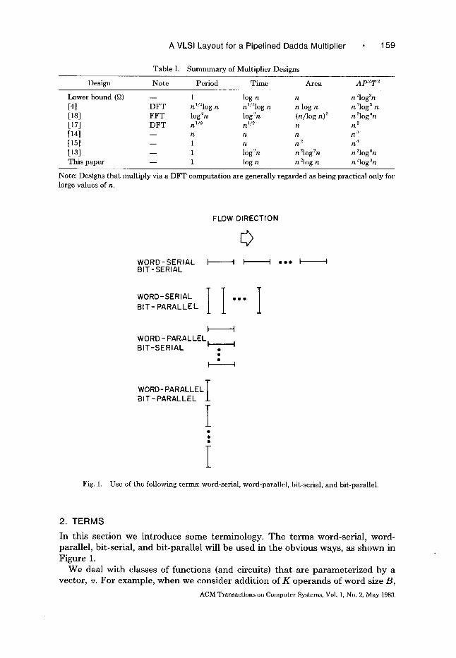
A VLSI Layout for a Pipelined Dadda Mult ipl ier
Table I. S u m m m a r y of Mult ipl ier Designs
159
Design Note Period T i m e Area A P 2 T ~
Lower bound (~) -- 1 log n n n210g2n [4] D F T n'/210g n nl/2log n n log n n~log 5 n [18] F F T logZn log2n (n/ log n) 2 nZlog4n [17] D F T n ' /2 n ]/2 n n ~
[14] - - n n n n '~ [15] -- 1 n n 2 n 4 [ 13] - - 1 log 2n n Clog 2n n 2log 6n Th i s paper - - 1 log n n 2log n n 21og:~n
Note: Designs tha t mult iply via a D F T computa t ion are generally regarded as being practical only for large values of n.
Fig. 1.
FLOW DIRECTION
WORD-SERIAL I I I I •,, I I
BIT-SERIAL
sE, ,AL [ I... I BIT - PARALLEL
WORD - PARALLEL BIT-SERIAL I
I
WORD- PARALLEL T BIT-PARALLEL .L
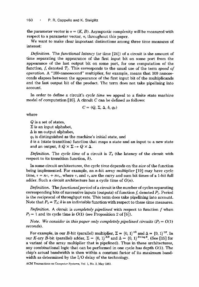
Use of the following terms: word-serial, word-parallel, bit-serial, and bit-paralleL
2. TERMS In this section we introduce some terminology. The t e rms word-serial, word- parallel, bit-serial, and bit-parallel will be used in the obvious ways, as shown in Figure 1.
We deal with classes of functions (and circuits) tha t are paramete r ized by a vector, 7r. For example, when we consider addit ion of K operands of word size B,
ACM Transactions on Computer Systems, Vol. 1, No. 2, May 1983.
160 P.R. Cappello and K. Steiglitz
the parameter vector is ~r = (K, B). Asymptotic complexity will be measured with respect to a parameter vector, % throughout this paper.
We want to make clear impor tant distinctions among three t ime measures of interest:
Definition. The functional latency (or t ime [24]) of a circuit is the amount of t ime separating the appearance of the first input bit on some port f rom the appearance of the last ou tput bit on some port, for one computa t ion of the function, f, denoted Tf. This corresponds to the usual use of the t e rm speed of operation. A "100-nanosecond" multiplier, for example, means tha t 100 nanose- conds elapses between the appearance of the first input bit of the multiplicands and the last ou tput bit of the product. The t e rm does not take pipelining into account.
In order to define a circuit 's cycle time we appeal to a finite s tate machine model of computat ion [10]. A circuit C can be defined as follows:
C = ( Q , Z , A , 8, qo)
where
Q is a set of states, E is an input alphabet, A is an output alphabet, q0 is distinguished as the machine 's initial state, and 8 is a {state transition) function tha t maps a state and an input to a new state and an output, 8:Q × Z --* Q × A.
Definition. The cycle time of a circuit is T8 (the latency of the circuit with respect to its transit ion function, 8).
In some circuit architectures, the cycle t ime depends on the size of the function being implemented. For example, an n-bi t array multiplier [19] m ay have cycle time, ~ = nTc + nTs, where rc and Ts are the carry and sum bit t imes of a 1-bit full adder. Such a circuit archi tecture has a cycle t ime of O(n).
Definition. The functionalperiod of a circuit is the number of cycles separating corresponding bits of successive inputs {outputs) of function f, denoted Pf. Per iod is the reciprocal of th roughput rate. This te rm does take pipelining into account. Note tha t P8 = Ts; 8 is an indivisible function with respect to these t ime measures.
Definition. A circuit is completely pipelined with respect to function f when Pf = 1 and its cycle t ime is O(1) (see Proposi t ion 2 of [6]).
Note. We consider in this paper only completely pipelined circuits (Pf = O(1) seconds).
For example, in our B-bit {parallel) multiplier, E = (0, 1} 2s and A = (0, 1} 2B. In our K-cry B-bit (parallel) adder, E = {0, 1} KR and h = {0, 1} B+logg. (See [15] for a variant of the array multiplier tha t is pipelined). Thus in these architectures, any combinational logic tha t can be performed in one cycle has dep th O(1). Th e chip's actual bandwidth is then within a constant factor of its maximum band- width as determined by the I /O delay of She technology.
ACM Transactions on Computer Systems, Vol. 1, No. 2, May 1983.
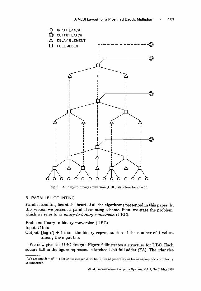
A VLSI Layout for a Pipelined Dadda Multiplier 161
Fig. 2. A u n a r y - t o - b i n a r y c o n v e r s i o n ( U B C ) s t r u c t u r e for B = 15.
3. PARALLEL COUNTING
Parallel counting lies at the heart of all the algorithms presented in this paper. In this section we present a parallel counting scheme. First, we state the problem, which we refer to as unary-to-binary conversion (UBC).
Problem: Unary-to-binary conversion (UBC) Input: B bits Output: [log BJ + 1 bits-- the binary representation of the number of 1 values
among the input bits
We now give the UBC design. 1 Figure 2 illustrates a structure for UBC. Each square (I-3) in the figure represents a latched 1-bit full adder (FA}. The triangles
W e a s s u m e B = 2 A" - 1 fo r s o m e i n t e g e r K w i t h o u t loss o f g e n e r a l i t y as f a r a s a s y m p t o t i c c o m p l e x i t y is c o n c e r n e d .
ACM Transact ions on Compute r Systems, Vol. 1, No. 2, May 1983.
162 .P.R. Cappello and K. Steiglitz
: i
t , i I i
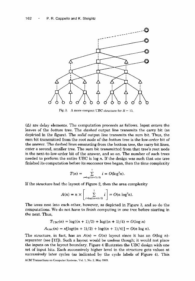
Fig. 3. A more compact UBC structure for B = 15.
(A) are delay elements. The computat ion proceeds as follows. Input enters the leaves of the b o t t o m tree. The d a s h e d output line t ransmits the carry bit (as depicted in the figure). The s o l i d output line t ransmits the sum bit. Thus, the sum bit t ransmit ted from the root node of the b o t t o m t ree is the low-order bit of the answer. The dashed lines emanat ing from the bo t tom tree, the carry bit lines, enter a second, smaller tree. The sum bit t ransmit ted from tha t tree 's root node is the next-to-low-order bit of the answer, and so on. Th e number of such trees needed to perform the entire UBC is log n. If the design was such tha t one tree finished its computat ion before its successor tree began, then the t ime complexi ty
1
T ( n ) = ~ i = O(log2n). i=log( (n+ l) /2)
If the s t ructure had the layout of Figure 2, then the area complexity
A ( n ) = n x F~ i = O ( n log2n). i=log( (n+ l) /2)
The trees nest into each other, however, as depicted in Figure 3, and so do the computations. We do not have to finish computing in one tree before starting in the next. Thus,
AvBc(n) = n[log((n + 1)/2) + log((n + 1)/4)] = O ( n log n).
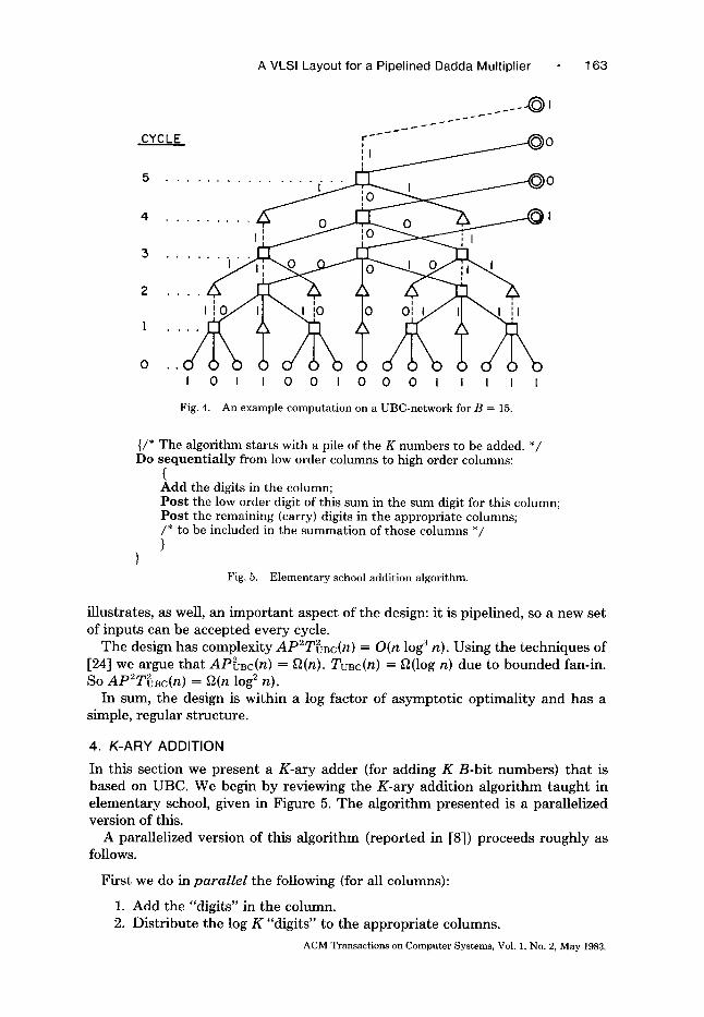
The structure, in fact, has an A ( n ) = O(n) layout since it has an O(log n)- separator (see [12]). Such a layout would be useless though; it would not place the inputs on the layout boundary. Figure 4 illustrates the UBC design with one set of input bits. Each successively higher level in the s t ructure gets values at successively later cycles (as indicated by the cycle labels of Figure 4). This
A C M T r a n s a c t i o n s o n C o m p u t e r S y s t e m s , V o l . 1, N o . 2, M a y 1983.
A VLSI Layout for a Pipelined Dadda Multiplier 163
CYCLE F . . . . . . . . ~ - ~ ) o
5 . . . . . . . . . . . ~ 0
4 . . . . . . . i ~ 1
3 . . . . . . . I ' " I
I . . . . 1"°'g/ II " ' ~ I ° o o ! ) ~ / i I " , < i l
o & I 0 I I 0 0 I 0 0 0 I I I
Fig. 4. An example computation on a UBC-network for B = 15.
{/* The algorithm starts with a pile of the K numbers to be added. */ Do sequentially from low order columns to high order columns:
( Add the digits in the column; Post the low order digit of this sum in the sum digit for this column; Post the remaining (carry) digits in the appropriate columns; /* to be included in the summation of those columns */ )
) Fig. 5. Elementary school addition algorithm.
illustrates, as well, an impor tant aspect of the design: it is pipelined, so a new set of inputs can be accepted every cycle.
The design has complexity APZT~Bc(n) = O(n log 3 n). Using the techniques of [24] we argue tha t AP~sc (n ) = ~2(n). Tvsc(n) = ~2(1og n) due to bounded fan-in. So A p 2 T ~ c ( n ) = ~2(n log 2 n).
In sum, the design is within a log factor of asymptot ic optimali ty and has a simple, regular structure.
4. K-ARY ADDITION
In this section we present a K-ary adder (for adding K B-bit numbers) tha t is based on UBC. We begin by reviewing the K-ary addition algori thm taught in e lementary school, given in Figure 5. The algori thm presented is a paraUelized version of this.
A parallelized version of this algorithm (reported in [8]) proceeds roughly as follows.
First we do in para l l e l the following (for all columns):
1. Add the "digits" in the column. 2. Distr ibute the log K "digits" to the appropriate columns.
ACM Transactions on Computer Systems, Vol. 1, No. 2, May 1983.
164 P.R. Cappello and K. Steiglitz
COLUMN 6 5 4 3 2 I
5 = 0 0 0 0 I 0 I - I0 - I I I 0 I I 0
I m 0 0 0 0 0 0 I -13 -= I I I 0 0 I I
12 " 0 0 0 I I 0 0 3 0 " 0 0 I I I I 0
COLUMN
6 5 4 3 2 1 0
ANSWER 0 0 1 I 0 0
BINARY ADD I I[ ,i II ,] I' I' I
BIT ~ ~ ~ ~ DISTRIBUTION OI OI II O0 OI I0 I
UBC A A A A A A A
010 010 OII I00 010 OII O0 I O,ST., UT, I
OBC A A A A A A A INPUT BITS 01OIOO OIOIOO 01OIOI OOOOII I10OII 01OIOI IOIIOO
6 5 4 3 2 1 0
Fig. 6. K-ary addition for K = 6, B = 7, sum = 25~() =- 0110012.
{ r e p e a t un t i l columns contain 2 bits
d o for all columns { perform UBC on the column; Distribute the sum bits; /* create new columns */ }
sum (-- carry-lookahead binary-addition; }
Fig. 7. A parallel K-ary addition algorithm.
T h e s e "d ig i t s " n o w c o n s t i t u t e new c o l u m n s to be a d d e d . W e h a v e r e d u c e d o u r K - a r y a d d i t i o n p r o b l e m to a log K - a r y a d d i t i o n p r o b l e m . T h e p r o c e s s is r e p e a t e d un t i l a b i n a r y a d d i t i o n p r o b l e m r e m a i n s . W e use a c a r r y - l o o k a h e a d b i n a r y a d d e r for t h e f ina l add i t i on .
W e p r o p o s e t h a t a V L S I i m p l e m e n t a t i o n of th i s a l g o r i t h m e m p l o y t h e U B C - n e t w o r k des ign of t h e p r e v i o u s sec t ion , a n d t h e a d d e r o f B r e n t a n d K u n g [5]. F i g u r e 6 shows t h e s t r u c t u r e a n d an e x a m p l e . F i g u r e 7 is a r e s t a t e m e n t o f t h e a l g o r i t h m t h a t a s s u m e s a b i n a r y n u m b e r r e p r e s e n t a t i o n .
ACM Transactions on Computer Systems, Vol. 1, No. 2, May 1983.
A VLSI Layout for a Pipelined Dadda Multiplier 165
We now analyze the period, latency, and area complexity of this design using the synchronous model of VLSI computation [3, 4].
Since the UBCs and binary adder [5] are completely pipelined, the entire K- ary B-bit adder is completely pipelined: Pg-add = 1 cycle.
The latency of this algorithm is the sum of the time to do the following.
1. Repeat block, which is the sum of the time for doing UBCs and bit distribution ("column" recreation).
2. B-bit parallel binary addition.
The asymptotic latency is
0 ( ~ ) log ~¢. log K) (UBC) Tadd(K, B ) =
fl(K)
+ ~ O(1) (Bit distribution) i~l
+ O(log B) (Binary addition)
= O ( l o g KB)
where fl(n) is a function that grows slower than log n, but is not a constant. See Appendix.
The area complexity is taken as the product of the width and length of the structure:
A a d d ( K , B) = O(KB) (Base) ~_F /~(~) ~ ) X / O ~ i__~ 1 log log K (UBC)
+ O | ~ log log K (Bit distribution) -1
+ O(log B) (Binary addition)
= O ( K B log KB)
The design has complexity AP2T2add(K, B) = O(KB log a KB). Using the techniques of [24], we argue that AP~dd(K, B) = ~(KB). Tadd(K, B) = ~2(log KB) due to bounded fan-in. So AP2T~dd(K, B) = £(KB log 2 KB).
Again, the design is within a log factor of asymptotic optimality and has a simple, regular structure.
5. BINARY MULTIPLICATION
In this section we present a binary multiplier. The algorithm, based on K-ary addition, is suggested by the following definition of binary multiplication. 2
B--1 x X y = Y, 2 b X x b X y (1)
b=0
We work with positive n u m b e r s wi thout loss of generality, a s suming two's comp lemen t ar i thmet ic . The s t ruc tures described here require a smal l modification to compute a product with 2B correct bits.
ACM Transactions on Computer Systems, Vol. 1, No. 2, May 1983.
166 P.R. Cappello and K. Steiglitz
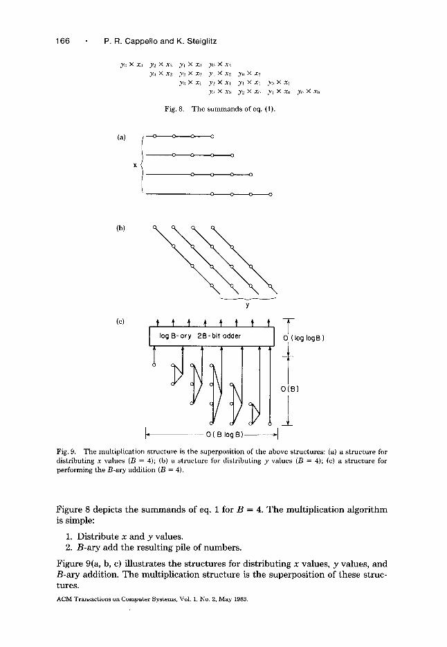
y3 X X:l y2 X X:I y , × x:~ y[) × x:~
y:~ X x~ y2 × x.-, y , × x2 y . × x._,
y:~ × x~ y2 X x, y~ X x~
y:~ x xo y., x x .
yo x x~ y~ x x .
Fig . 8. The summands of eq. (1).
y . x xo
(a) ~ 0 0
"I o °o
0
0 0
0 0
0 0
(b)
Y
(c) t t ~ ~ ~ t t J log B-ory 2B-bit odder T
0 (log IogB )
O(B)
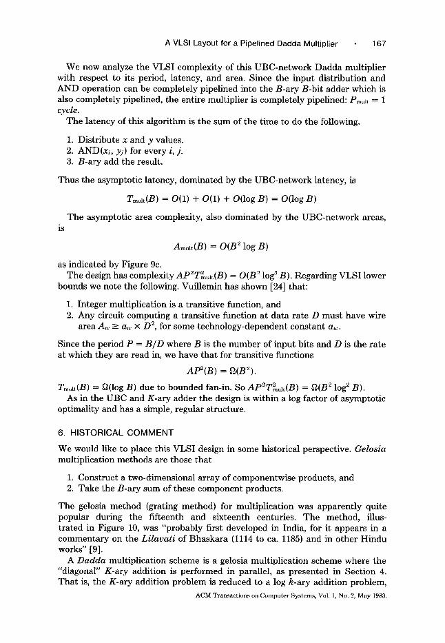
A_ ., O( B logB) ~]
Fig. 9. The multiplication structure is the superposition of the above structures: (a) a s t r u c t u r e fo r
distributing x values (B = 4); (b) a s t r u c t u r e fo r d i s t r i b u t i n g y v a l u e s (B = 4); (c) a s t r u c t u r e fo r
performing the B-ary addition (B = 4).
Figure 8 depicts the summands of eq. 1 for B = 4. The multiplication algorithm is simple:
1. Distribute x and y values. 2. B-ary add the resulting pile of numbers.
Figure 9(a, b, c) illustrates the structures for distributing x values, y values, and B-ary addition. The multiplication structure is the superposition of these struc- tures.
ACM Transact ions on Computer Systems, Vol. 1, No. 2, May 1983.
A VLSI Layout for a Pipelined Dadda Multiplier 167
We now analyze the VLSI complexity of this UBC-network Dadda multiplier with respect to its period, latency, and area. Since the input distribution and AND operation can be completely pipelined into the B-ary B-bit adder which is also completely pipelined, the entire multiplier is completely pipelined: Pmuit - - 1 cycle.
The latency of this algorithm is the sum of the time to do the following.
1. Distribute x and y values. 2. AND(xi, yj) for every i, j . 3. B-ary add the result.
Thus the asymptotic latency, dominated by the UBC-network latency, is
is
T mul t (B ) = O ( 1 ) -I- O ( 1 ) -4- O(log B) = O(log B )
The asymptotic area complexity, also dominated by the UBC-network areas,
A m u l t ( B ) = O(B z log B)
as indicated by Figure 9e. The design has complexity APZT2olt(B) = O(B 2 log3 B). Regarding VLSI lower
bounds we note the following. Vuillemin has shown [24] that:
1. Integer multiplication is a transitive function, and 2. Any circuit computing a transitive function at data rate D must have wire
area Aw >- aw x D 2, for some teehnology-dependent constant aw.
Since the period P = B I D where B is the number of input bits and D is the rate at which they are read in, we have that for transitive functions
AP2(B) = ~2(B2).
Tmult(B) = ~(log B) due to bounded fan-in. So APZT2ult(B) = ~2(B 2 log 2 B). As in the UBC and K-ary adder the design is within a log factor of asymptotic
optimality and has a simple, regular structure.
6. HISTORICAL COMMENT
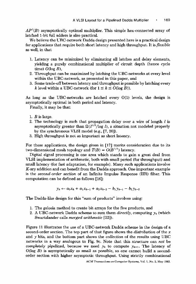
We would like to place this VLSI design in some historical perspective. Gelosia multiplication methods are those that
1. Construct a two-dimensional array of componentwise products, and 2. Take the B-ary sum of these component products.
The gelosia method (grating method) for multiplication was apparently quite popular during the fifteenth and sixteenth centuries. The method, illus- trated in Figure 10, was "probably first developed in India, for it appears in a commentary on the Lilavati of Bhaskara (1114 to ca. 1185) and in other Hindu works" [9].
A Dadda multiplication scheme is a gelosia multiplication scheme where the "diagonal" K-ary addition is performed in parallel, as presented in Section 4. That is, the K-ary addition problem is reduced to a log k-ary addition problem,
ACM Transactions on Computer Systems, Vol. 1, No. 2, May 1983.
168 P.R. Cappel lo and K. Steiglitz
GELOSIA METHOD
MULTIPLICAND
0 D
0 rv"
6
0
7/, 7
7
o / /7 / ,
/
/ , / . / , S
2
9
S /7
6
2
4
n - w _1 n
D
IN GRATING ABOVE, ADDITIONS ARE PERFORMED DIAGONALLY
6789 x 1254= 8377626
Fig. 10. Gelosia method for multiplication (after [9]). (In the grating illustrated above, addit ions are performed diagonally.
and that is reduced to a loglog k-ary addition problem, and so on, until a binary addition problem remains. In order to achieve asymptotic optimality with respect to period and latency, this approach requires performing the following:
1. Unary-to-binary conversions asymptotically optimally, and 2. Final binary addition asymptotically optimally.
The adder in [5] does the latter, the UBC-network of Section 3 does the former. And, what is important for VLSI implementation, they do them with simple, regular, compact layouts.
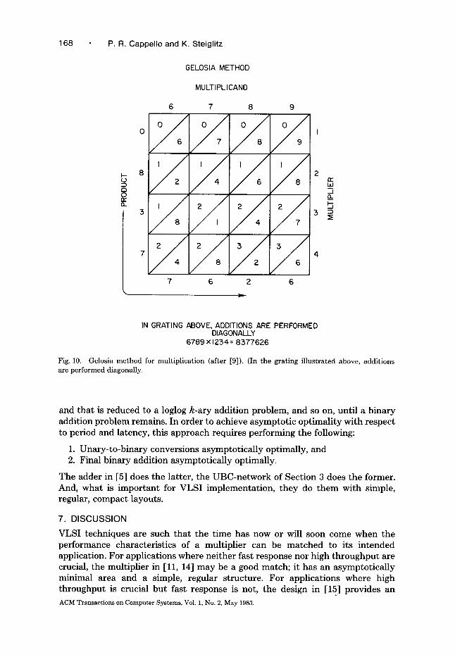
7. D ISCUSSION
VLSI techniques are such that the time has now or will soon come when the performance characteristics of a multiplier can be matched to its intended application. For applications where neither fast response nor high throughput are crucial, the multiplier in [11, 14] may be a good match; it has an asymptotically minimal area and a simple, regular structure. For applications where high throughput is crucial but fast response is not, the design in [15] provides an ACM Transactions on Computer Systems, Vol. 1, No. 2, May 1983.
A VLSI Layout for a Pipelined Dadda Multiplier 169
AP2(B) asymptotically optimal multiplier. This simple hex-connected array of latched 1-bit full adders is also practical.
We believe the UBC-network Dadda design presented here is a practical design for applications that require both short latency and high throughput. It is flexible as well, in that
1. Latency can be minimized by eliminating all latches and delay elements, yielding a purely combinational multiplier of circuit depth (hence cycle time) O(log B),
2. Throughput can be maximized by latching the UBC-networks at every level within the UBC-network, as presented in this paper, and
3. Some trade-off between latency and throughput is possible by latching every k level within a UBC-network (for 1 __ k __ O(log B)).
As long as the UBC-networks are latched every asymptotically optimal in both period and latency.
Finally, it may be that:
O(1) levels, the design is
1. B is large. 2. The technology is such that propagation delay over a wire of length l is
asymptotically greater than ~(ll/2/log l), a situation not modeled properly by the synchronous VLSI model (e.g., [7, 20]).
3. High throughput is not as important as short latency.
For these applications, the design given in [17] merits consideration due to its two-dimensional mesh topology and T(B) = O(B 1/2) latency.
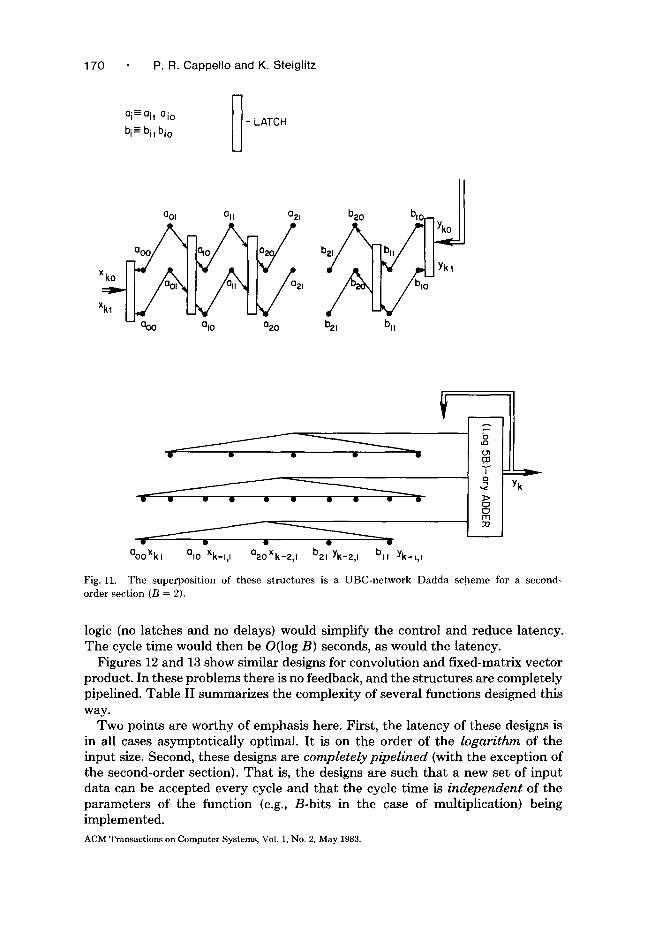
Digital signal processing is one area which stands to gain a great deal from VLSI implementation of arithmetic, both with small period (for throughput} and small latency (for fast adaptation, for example). Many such applications involve K-ary addition and can benefit from the Dadda approach. One important example is the second-order section of an Infinite Impulse Response (IIR) filter. This computation can be defined as follows [16]:
y k <--- a o X k + a l x k - 1 + a 2 X k - 2 - - b l y k - 1 - - b 2 y k - 2
The Dadda-like design for this "sum of products" involves using:
1. The gelosia method to create bit arrays for the five products, and 2. A UBC-network Dadda scheme to sum them directly, computing yh (which
Swartzlander calls merged arithmetic [22]).
Figure 11 illustrates the use of a UBC-network Dadda scheme in the design of a second-order section. The top part of that figure shows the distribution of the x and y bits, and the bottom part shows the collection of the results using UBC networks in a way analogous to Fig. 9c. Note that this structure can not be completely pipelined, because we need yk to compute yk+l. The latency of O(log B) is asymptotically as small as possible, so one cannot build a second- order section with higher asymptotic throughput. Using strictly combinational
ACM Transactions on Computer Systems, Vol. 1, No. 2, May 1983.
170 P.R. Cappello and K. Steiglitz
ai-= air Oio ~ - bi= bil bio
LATCH
H 001 OI I 021 b20 b=or-t II
LF / u,,v LIV %o alo aao b21 bH
aooXkl °lO Xk-i# °2oXk-2,t b21 Yk-2,i btl Yk-l , i
4_. I
,~ Yk O O rrl
Fig. 11. The superposition of these structures is a UBC-network Dadda scheme for a second- order section (B = 2).
logic (no latches and no delays) would simplify the control and reduce latency. The cycle time would then be O(log B) seconds, as would the latency.
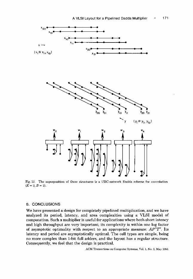
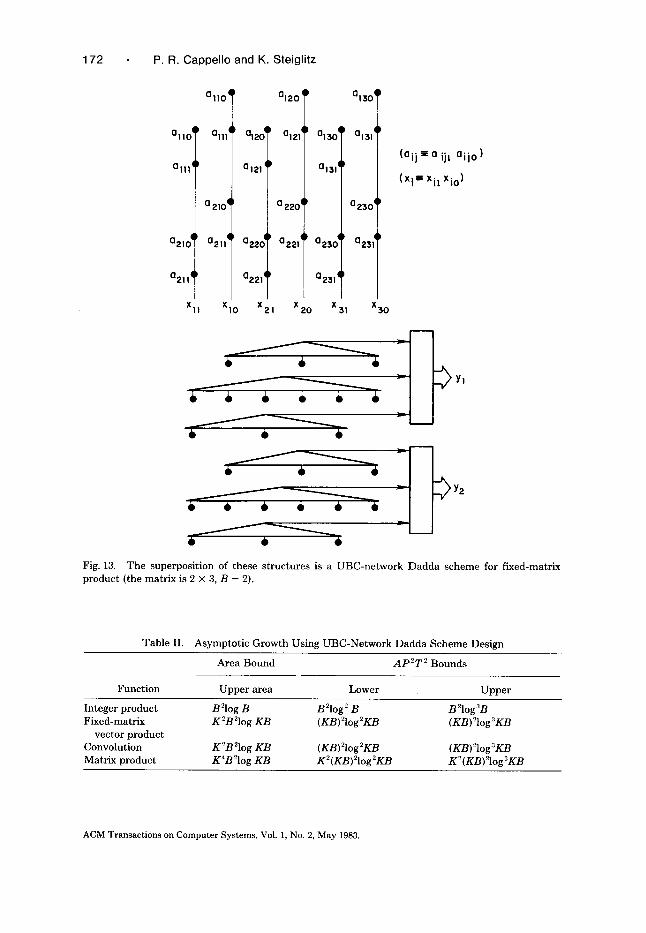
Figures 12 and 13 show similar designs for convolution and fixed-matrix vector product. In these problems there is no feedback, and the structures are completely pipelined. Table II summarizes the complexity of several functions designed this way.
Two points are worthy of emphasis here. First, the latency of these designs is in all cases asymptotically optimal. It is on the order of the logarithm of the input size. Second, these designs are completely pipelined {with the exception of the second-order section). That is, the designs are such that a new set of input data can be accepted every cycle and that the cycle time is independent of the parameters of the function (e.g., B-bits in the case of multiplication) being implemented.
ACM Transact ions on Computer Systems, Vol. 1, No. 2, May 1983.
A VLSI Layout for a Pipelined Dadda Multiplier 1 71
X O 0 ; A A
XOI ¢ ~-
XIO -~ C
Xl l " X ~
(xi~ xil Xio)
A A
A C =- =-- --=
X 2 0 : - , , A A
Yoo Yol Ylo Yu Y2o YZl
Y (Y i --= Y i l Y io )
iltillit Fig. 12. The superposition of these structures is a UBC-network Dadda scheme for convolution (K= 3, B = 2).
8. C O N C L U S I O N S
We have presented a design for complete ly pipelined multiplication, and we have analyzed its period, latency, and area complexit ies using a VLSI model of computat ion. Such a mult ipl ier is useful for applicat ions where bo th shor t la tency and high th roughpu t are very important ; its complexi ty is within one log factor of asymptot ic opt imal i ty with respect to an appropr ia te measure: A P 2 T 2. I ts la tency and period are asymptot ica l ly optimal. T h e cell types are simple, being no more complex than 1-bit full adders, and the layout has a regular s tructure. Consequently, we feel tha t the design is practical.
ACM Transactions on Computer Systems, Vol. 1, No. 2, May 1983.
172 P.R. Cappello and K. Steiglitz
0110 q
0111 q
02,o ~
02114
Xll
0110 i
al l l q
0 210 !
02114
Xlo
0120 i
0120 q 0121
3121
0 2204
3220~ 0221 ~ I
:1221 t
X21 Xzo
0130 i
01311
023o q
Q231 i
X31
0130i I
01311D
0230 i P
a231T X30
(ai j .=- a ij| a i jo )
( x i i x i l Xio)
_1
• • • • • • / Fig. 13. The superposition of these structures is a UBC-network Dadda scheme for fixed-matrix product (the matrix is 2 x 3, B = 2).
Table II. Asymptotic Growth Using UBC-Network Dadda Scheme Design
Area Bound ApeT 2 Bounds
Function Upper area Lower Upper
Integer product B Slog B B 210ge B B 210g3B Fixed-matrix K2B210g KB (KB)210g2KB (KB)210g3KB
ACM Transactions on Computer Systems, Vol. 1, No. 2, May 1983.
A VLSI Layout for a Pipelined Dadda Multiplier 173
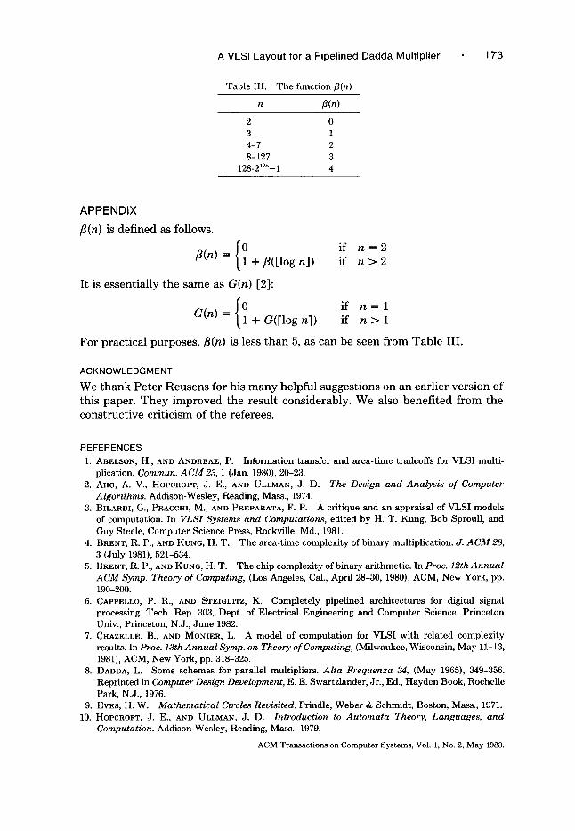
Table III. The function fl(n)
n fi(n)
2 0 3 1 4-7 2 8-127 3
128-212s-1 4
APPENDIX
f l (n) is defined as follows.
{0 if n = 2 f l (n) = + fi([log n J) if n > 2
It is essentially the same as G(n) [2]:
{0 if n = l G ( n ) = + G(rlog n]) i f n > 1
For practical purposes, f l (n) is less than 5, as can be seen from Table III.
ACKNOWLEDGMENT
We thank Peter Reusens for his many helpful suggestions on an earlier version of this paper. They improved the result considerably. We also benefi ted from the constructive criticism of the referees.
REFERENCES 1. ABELSON, H., AND ANDREAE, P. Information transfer and area-time tradeoffs for VLSI multi-
plication. Commun. ACM 23, 1 (Jan. 1980), 20-23. 2. AHO, A. V., HOPCROFT, J. E., AND ULLMAN, Z. D. The Design and Analysis of Computer
Algorithms. Addison-Wesley, Reading, Mass., 1974. 3. BILARDI, G., PRACCHI, M., AND PREPARATA, F.P. A critique and an appraisal of VLSI models
of computation. In VLSI Systems and Computations, edited by H. T. Kung, Bob Sproull, and Guy Steele, Computer Science Press, Rockville, Md., 1981.
4. BRENT, R. P., AND KUNG, H.W. The area-time complexity of binary multiplication. J. ACM 28, 3 (July 1981), 521-534.
5. BRENT, R. P., AND KUNG, S . T . The chip complexity of binary arithmetic. In Proc. 12th Annual ACM Syrup. Theory of Computing, (Los Angeles, Cal., April 28-30, 1980), ACM, New York, pp. 190-200.
6. CAPPELLO, P. a. , AND STEIGLITZ, K. Completely pipelined architectures for digital signal processing. Tech. Rep. 303, Dept. of Electrical Engineering and Computer Science, Princeton Univ., Princeton, N.J., June 1982.
7. CHAZELLE, B., AND MONIER, L. A model of computation for VLSI with related complexity results. In Proc. 13th Annual Syrup. on Theory of Computing, (Milwaukee, Wisconsin, May 11-13, 1981), ACM, New York, pp. 318-325.
8. DADDA, L. Some schemes for parallel multipliers. Alta Frequenza 34, (May 1965), 349-356. Reprinted in Computer Design Development, E. E. Swartzlander, Jr., Ed., Hayden Book, Rochelle Park, N.J., 1976.
9. EVES, H.W. Mathematical Circles Revisited. Prindle, Weber & Schmidt, Boston, Mass., 1971. 10. HOPCROFT, J. E., AND ULLMAN, J. D. Introduction to Automata Theory, Languages, and
ACM Transactions on Computer Systems, Vol. 1, No. 2, May 1983.
174 P.R. Cappello and K. Steiglitz
11. JACKSON, L. B., KAISER, S. F., AND McDONALD, H.S . An approach to the implementation of digital filters. IEEE Trans. Audio and Electro-Acoustic, A U.16 (Sept. 1968), 413-421.
12. LEISERSON, C.E. Area-efficient graph layouts (for VLSI). In Proc. IEEE 21st Annual Syrup. Foundations of Computer Science. Syracuse, N.Y., 1980.
13. LUK, W.K. A regular layout for parallel multiplier of O(log 2 n) time. In VLSI Systems and Computations, H. T. Kung, Bob Sproull, and Guy Steele, Eds., Computer Science Press, Rockville, Md., 1981.
14. LYON, R. F. Two's complement pipeline multipliers. IEEE Trans. Comm., COM-24, 4 (April 1976), 418-425.
15. MCCANNY, J. V., MCWHIRTER, J. G., ROBERTS, J. B. G., DAY, D. J., AND THORP, T.L. Bit level systolic arrays. In Proc. 15th Asilomar Conf. on Circuits, Systems, & Computers, Nov. 1981.
16. OPPENHEIM, A. V., AND SCHAFER, R.W. Digital Signal Processing. Prentice-Hall, Englewood Cliffs, N.J., 1975.
17. PREPARATA, F . P . A mesh-connected area-time optimal VLSI integer multiplier. In VLSI Systems and Computations, H. T. Kung, Bob Sproull, and Guy Steele, Eds., Computer Science Press, RockviUe, Md., 1981.
18. PREPARATA, F. P., AND VUILLEMIN, J.E. The cube-connected-cycles: A versatile network for parallel computation. Commun. ACM 24, 5 (May 1981), 300-309.
19. RABINER, L. R., AND GOLD, B. Theory and Application of Digital Signal Processing, Prentice- Hall, Englewood Cliffs, N.J., 1975.
20. RAMACHANDRAN, V. On driving many long wires in a VLSI layout. Tech. Rep. 300, Department of Electrical Engineering and Computer Science, Princeton, Univ., Princeton, N.J., April 1982.
21. REUSENS, P., KU, W., AND MAO, V. Fixed-point high-speed multipliers in VLSI. In VLSI Systems and Computations, H. T. Kung, Bob Sproull, and Guy Steele, Eds., Computer Science Press, Rockville, Md., 1981.
22. SWARTZLANDER, E. E., JR., Merged arithmetic for signal processing. In Proc. IEEE 4th Syrup. Computer Arithmetic, Santa Monica, Calif., 1978.
23. THOMPSON, C. D. Area-time complexity for VLSI. In Proc. 11th Annual Symp. Theory of Computing, (Atlanta, Georgia, April 3O-May 2, 1979), ACM, New York, pp. 81-88.
24. VUILLEMIN, J. A combinatorial limit to the computing power of VLSI circuits. In Proc. IEEE 21st Annual Symposium of Foundations of Computer Science. Syracuse, N.Y., 1980.
Received October 1981; revised June 1982; accepted November 1982
ACM Transactions on Computer Systems, Vol. 1, No. 2, May 1983.