Aalborg Universitet Prediction of Short-Circuit-Related Thermal Stress in Aged IGBT Modules Bahman, Amir Sajjad; Iannuzzo, Francesco; Uhrenfeldt, Christian; Blaabjerg, Frede; Munk- Nielsen, Stig Published in: Proceedings of IEEE Energy Conversion Congress and Exposition (ECCE), 2016 DOI (link to publication from Publisher): 10.1109/ECCE.2016.7855365 Publication date: 2016 Document Version Accepted author manuscript, peer reviewed version Link to publication from Aalborg University Citation for published version (APA): Bahman, A. S., Iannuzzo, F., Uhrenfeldt, C., Blaabjerg, F., & Munk-Nielsen, S. (2016). Prediction of Short- Circuit-Related Thermal Stress in Aged IGBT Modules. In Proceedings of IEEE Energy Conversion Congress and Exposition (ECCE), 2016 IEEE Press. https://doi.org/10.1109/ECCE.2016.7855365 General rights Copyright and moral rights for the publications made accessible in the public portal are retained by the authors and/or other copyright owners and it is a condition of accessing publications that users recognise and abide by the legal requirements associated with these rights. ? Users may download and print one copy of any publication from the public portal for the purpose of private study or research. ? You may not further distribute the material or use it for any profit-making activity or commercial gain ? You may freely distribute the URL identifying the publication in the public portal ? Take down policy If you believe that this document breaches copyright please contact us at [email protected] providing details, and we will remove access to the work immediately and investigate your claim. Downloaded from vbn.aau.dk on: October 29, 2021
Transcript
Aalborg Universitet
Prediction of Short-Circuit-Related Thermal Stress in Aged IGBT Modules
Bahman, Amir Sajjad; Iannuzzo, Francesco; Uhrenfeldt, Christian; Blaabjerg, Frede; Munk-Nielsen, StigPublished in:Proceedings of IEEE Energy Conversion Congress and Exposition (ECCE), 2016
DOI (link to publication from Publisher):10.1109/ECCE.2016.7855365
Publication date:2016
Document VersionAccepted author manuscript, peer reviewed version
Link to publication from Aalborg University
Citation for published version (APA):Bahman, A. S., Iannuzzo, F., Uhrenfeldt, C., Blaabjerg, F., & Munk-Nielsen, S. (2016). Prediction of Short-Circuit-Related Thermal Stress in Aged IGBT Modules. In Proceedings of IEEE Energy Conversion Congressand Exposition (ECCE), 2016 IEEE Press. https://doi.org/10.1109/ECCE.2016.7855365
General rightsCopyright and moral rights for the publications made accessible in the public portal are retained by the authors and/or other copyright ownersand it is a condition of accessing publications that users recognise and abide by the legal requirements associated with these rights.
? Users may download and print one copy of any publication from the public portal for the purpose of private study or research. ? You may not further distribute the material or use it for any profit-making activity or commercial gain ? You may freely distribute the URL identifying the publication in the public portal ?
Take down policyIf you believe that this document breaches copyright please contact us at [email protected] providing details, and we will remove access tothe work immediately and investigate your claim.
Abstract— In this paper, the thermal stress on bond wires of aged IGBT modules under short-circuit conditions has been studied with respect to different solder delamination levels. To ensure repeatable test conditions, ad-hoc DBC (direct bond copper) samples with delaminated solder layers have been purposely fabricated. The temperature distribution produced by such abnormal conditions has been modelled first by means of FEM simulations and then experimentally validated by means of a non-destructive testing technique including an ultra-fast infrared camera. Results demonstrate a significant imbalance in the surface temperature distribution which confirms the hypothesis that short-circuit events produce significantly uneven stresses on bond wires.
Insulated Gate Bipolar Transistor (IGBT) modules are widely used in many high-power applications, e.g. wind turbines, ships and trains [1]-[3]. Due to the high fabrication costs of IGBT modules as well as maintenance costs in the application, higher lifetime is required and stringent reliability constraints are assigned to meet the trend in the sustainability of power electronic systems. Besides, the current trend in the IGBT module fabrication is to achieve greater power density, higher switching frequency and smaller volume. This trend induces more dynamic loading and higher operating temperatures, thus making more fatigue and a higher failure rate if not designed properly [4].
Generally speaking, power semiconductor devices account for 20% of total failures occurring in power converter systems [5], [6]. It has been proven that ageing of bond wires and solder fatigue caused by power cycling are the dominant failure mechanisms in IGBT modules [7]. Indeed, IGBT failures are not directly caused by solder fatigue, but rather by bond wire lift-off, which has a wear-out nature which is developing gradually during operation [8]. Therefore, both mechanisms are coupled, since the solder joint degradation under the chip produces a local temperature increase that can accelerate the bond wire lift-off. On top of that, due to the harsh environmental conditions IGBT modules operate in, abnormal situations happen frequently, causing random and severe thermal and mechanical stresses. The corresponding stresses significantly affect the reliability of the IGBT module, ending up in a large uncertainty in the lifetime estimation. Therefore,
understanding and prediction of the current, temperature and strain distributions in such cases are important for a reliable design [9].
In the past research works, thermal stresses on IGBT modules have been mostly investigated under normal operating conditions such as thermal cycling and power cycling [10]-[14]. However, abnormal operations like short-circuit or overloads are critical and should be considered if a confident life-time prediction is targeted. The problem becomes more severe in presence of an aged part such as delaminated solder in an IGBT module [15]. The well-known techniques such as derating or redundancy of devices are not a solution as they considerably increases the product cost, but a Design-For-Reliability (DFR) approach can increase the confidence level on the expected life-time and therefore reduce the design margin by taking into account the effects of abnormal operations [7]. One condition to correctly adopt such an approach, though, is to take into account the mixed failure mechanisms from the very beginning of the design process [16].
To this aim, this paper investigates the thermal stress generated in short-circuit condition on bond wires of aged IGBT modules. Finite-Element Method (FEM) simulations are applied to extract the temperature profiles at the surface of the IGBT chip for different solder joint delamination levels. The most thermal stressed bond wires are identified and the thermal stresses on them are estimated, which are caused by thermal expansion mismatch in the silicon/aluminum interface. Mixed ageing and short-circuit experiments are hard to be done, especially because the given ageing levels are hardly achievable in a systematic way. Consequently, an ad-hoc set of DBC (direct bond copper) samples at different delamination levels has been purposely developed and experiments have been carried out on them to validate the predicted phenomenon.
II. MODELING THE AGEING OF THE IGBT MODULE IN SHORT-CIRCUIT CONDITION
A. Ageing mechanisms in the IGBT module
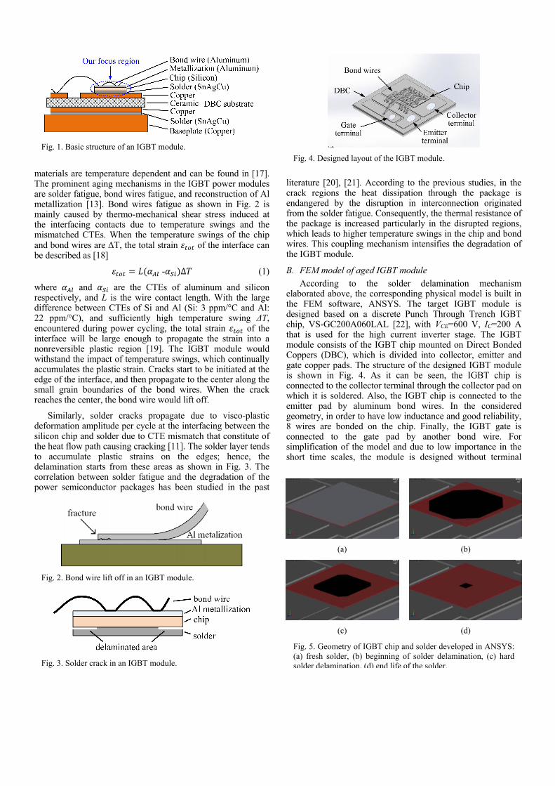
The IGBT module is characterized by semiconductor chips bonded to metal conductors with thick parallel aluminum bond wires on an insulating dielectric layer by means of solder. The IGBT module as shown in Fig. 1 has a multi-layer structure consisting of different materials with different Coefficient of Thermal Expansion (CTE). The thermal properties of the
materials are temperature dependent and can be found in [17]. The prominent aging mechanisms in the IGBT power modules are solder fatigue, bond wires fatigue, and reconstruction of Al metallization [13]. Bond wires fatigue as shown in Fig. 2 is mainly caused by thermo-mechanical shear stress induced at the interfacing contacts due to temperature swings and the mismatched CTEs. When the temperature swings of the chip and bond wires are ΔT, the total strain of the interface can be described as [18]
= ( - )∆ (1)
where and are the CTEs of aluminum and silicon respectively, and L is the wire contact length. With the large difference between CTEs of Si and Al (Si: 3 ppm/°C and Al: 22 ppm/°C), and sufficiently high temperature swing ΔT, encountered during power cycling, the total strain of the interface will be large enough to propagate the strain into a nonreversible plastic region [19]. The IGBT module would withstand the impact of temperature swings, which continually accumulates the plastic strain. Cracks start to be initiated at the edge of the interface, and then propagate to the center along the small grain boundaries of the bond wires. When the crack reaches the center, the bond wire would lift off.
Similarly, solder cracks propagate due to visco-plastic deformation amplitude per cycle at the interfacing between the silicon chip and solder due to CTE mismatch that constitute of the heat flow path causing cracking [11]. The solder layer tends to accumulate plastic strains on the edges; hence, the delamination starts from these areas as shown in Fig. 3. The correlation between solder fatigue and the degradation of the power semiconductor packages has been studied in the past
literature [20], [21]. According to the previous studies, in the crack regions the heat dissipation through the package is endangered by the disruption in interconnection originated from the solder fatigue. Consequently, the thermal resistance of the package is increased particularly in the disrupted regions, which leads to higher temperature swings in the chip and bond wires. This coupling mechanism intensifies the degradation of the IGBT module.
B. FEM model of aged IGBT module
According to the solder delamination mechanism elaborated above, the corresponding physical model is built in the FEM software, ANSYS. The target IGBT module is designed based on a discrete Punch Through Trench IGBT chip, VS-GC200A060LAL [22], with VCE=600 V, IC=200 A that is used for the high current inverter stage. The IGBT module consists of the IGBT chip mounted on Direct Bonded Coppers (DBC), which is divided into collector, emitter and gate copper pads. The structure of the designed IGBT module is shown in Fig. 4. As it can be seen, the IGBT chip is connected to the collector terminal through the collector pad on which it is soldered. Also, the IGBT chip is connected to the emitter pad by aluminum bond wires. In the considered geometry, in order to have low inductance and good reliability, 8 wires are bonded on the chip. Finally, the IGBT gate is connected to the gate pad by another bond wire. For simplification of the model and due to low importance in the short time scales, the module is designed without terminal
Fig. 1. Basic structure of an IGBT module.
Fig. 2. Bond wire lift off in an IGBT module.
Fig. 3. Solder crack in an IGBT module.
Fig. 4. Designed layout of the IGBT module.
(a)
(b)
(c)
(d)
Fig. 5. Geometry of IGBT chip and solder developed in ANSYS: (a) fresh solder, (b) beginning of solder delamination, (c) hard solder delamination, (d) end life of the solder.
leads and baseplate.
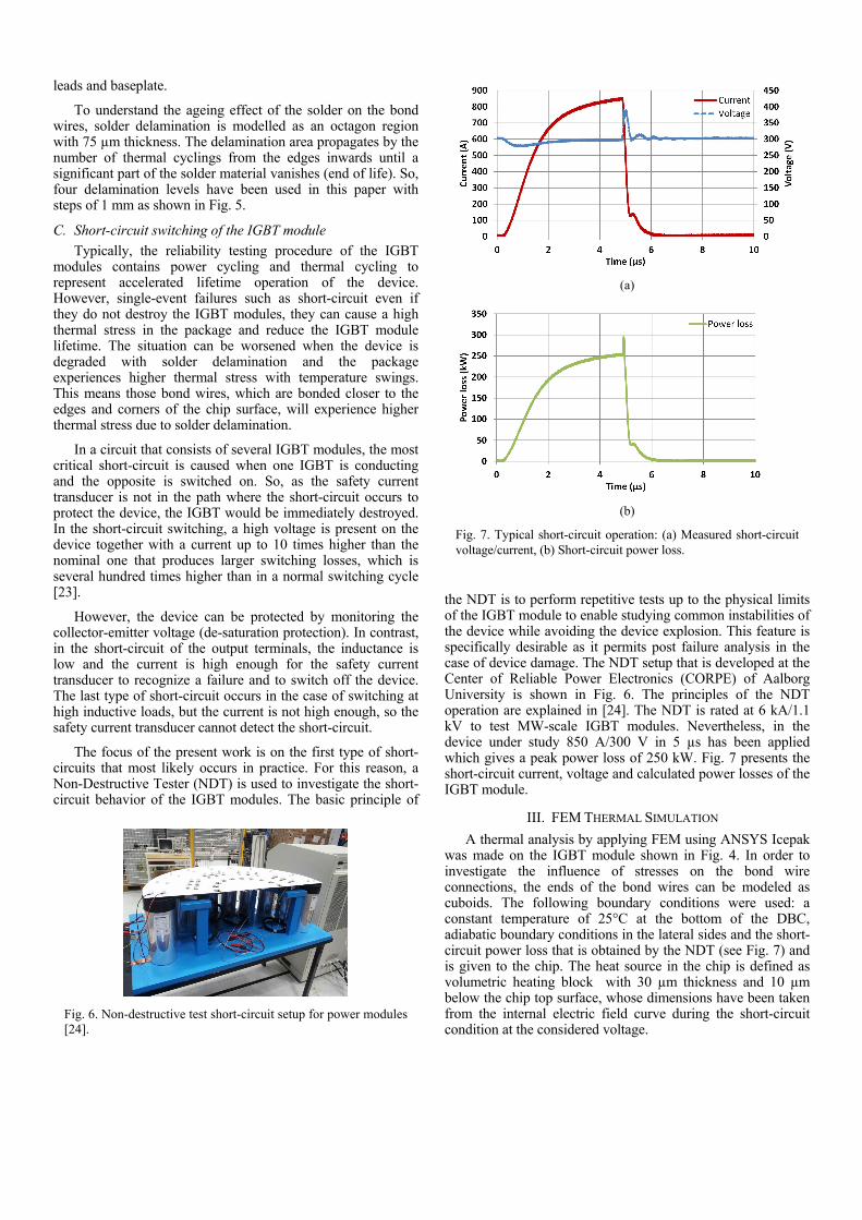
To understand the ageing effect of the solder on the bond wires, solder delamination is modelled as an octagon region with 75 µm thickness. The delamination area propagates by the number of thermal cyclings from the edges inwards until a significant part of the solder material vanishes (end of life). So, four delamination levels have been used in this paper with steps of 1 mm as shown in Fig. 5.
C. Short-circuit switching of the IGBT module
Typically, the reliability testing procedure of the IGBT modules contains power cycling and thermal cycling to represent accelerated lifetime operation of the device. However, single-event failures such as short-circuit even if they do not destroy the IGBT modules, they can cause a high thermal stress in the package and reduce the IGBT module lifetime. The situation can be worsened when the device is degraded with solder delamination and the package experiences higher thermal stress with temperature swings. This means those bond wires, which are bonded closer to the edges and corners of the chip surface, will experience higher thermal stress due to solder delamination.
In a circuit that consists of several IGBT modules, the most critical short-circuit is caused when one IGBT is conducting and the opposite is switched on. So, as the safety current transducer is not in the path where the short-circuit occurs to protect the device, the IGBT would be immediately destroyed. In the short-circuit switching, a high voltage is present on the device together with a current up to 10 times higher than the nominal one that produces larger switching losses, which is several hundred times higher than in a normal switching cycle [23].
However, the device can be protected by monitoring the collector-emitter voltage (de-saturation protection). In contrast, in the short-circuit of the output terminals, the inductance is low and the current is high enough for the safety current transducer to recognize a failure and to switch off the device. The last type of short-circuit occurs in the case of switching at high inductive loads, but the current is not high enough, so the safety current transducer cannot detect the short-circuit.
The focus of the present work is on the first type of short-circuits that most likely occurs in practice. For this reason, a Non-Destructive Tester (NDT) is used to investigate the short-circuit behavior of the IGBT modules. The basic principle of
the NDT is to perform repetitive tests up to the physical limits of the IGBT module to enable studying common instabilities of the device while avoiding the device explosion. This feature is specifically desirable as it permits post failure analysis in the case of device damage. The NDT setup that is developed at the Center of Reliable Power Electronics (CORPE) of Aalborg University is shown in Fig. 6. The principles of the NDT operation are explained in [24]. The NDT is rated at 6 kA/1.1 kV to test MW-scale IGBT modules. Nevertheless, in the device under study 850 A/300 V in 5 µs has been applied which gives a peak power loss of 250 kW. Fig. 7 presents the short-circuit current, voltage and calculated power losses of the IGBT module.
III. FEM THERMAL SIMULATION
A thermal analysis by applying FEM using ANSYS Icepak was made on the IGBT module shown in Fig. 4. In order to investigate the influence of stresses on the bond wire connections, the ends of the bond wires can be modeled as cuboids. The following boundary conditions were used: a constant temperature of 25°C at the bottom of the DBC, adiabatic boundary conditions in the lateral sides and the short-circuit power loss that is obtained by the NDT (see Fig. 7) and is given to the chip. The heat source in the chip is defined as volumetric heating block with 30 µm thickness and 10 µm below the chip top surface, whose dimensions have been taken from the internal electric field curve during the short-circuit condition at the considered voltage.
Fig. 6. Non-destructive test short-circuit setup for power modules [24].
The FEM simulations are carried out for 1 second with varying time steps that start with smaller time steps and end in longer steps to reduce the simulation time. The short-circuit power loss is injected to the heat source for 5 μs. Two cases with fresh solder and hard solder delamination have been compared and it is shown in Fig. 8. As assumed, in the model with solder delamination the outmost corners of the IGBT chip are the most stressed ones. The delamination area propagates by the number of thermal cyclings from the edges inwards until a significant part of the solder material vanishes (end of life) [12]. Solder delamination induces an inhomogeneous temperature field, which causes an increased stress in the regions above the delaminated area (including the chip surface).
For a better explanation, three bond wire foot positions have been selected (highlighted in Fig. 8) and their temperature profiles are extracted. As it is observed in Fig. 9, the peak temperature is identical for all cases, since the heat up is almost adiabatically due to the time frame of the power loss. However, after 1 ms, the generated heat propagates to the solder layer. In the delaminated solder condition, both bond wire foot positions at the edge and center show higher temperature response due to higher thermal resistance of the IGBT module. The reason originates from the delamination propagating from corners, hence the last remaining solder material is under the center of the IGBT chip. So, unlike to the fresh solder condition that the center bond wire experiences a higher thermal stress, in the delaminated solder condition, edge bond wire is stressed considerably higher than the center bond wire. Moreover, in
the time intervals after 1 ms, all of bond wires in the aged module (delaminated) are stressed up to 70% higher than the case of a fresh device. That in the case of large short-circuit currents, they may lift off immediately. On the other hand, the cooling system is not effective in short time scales due to the thermal capacitance of several layers underneath the IGBT chip. This analysis for the case of short-circuit can be generalized for the cases of normal thermal cycling with large dynamic loading in real applications.
IV. EXPERIMENTAL VALIDATION AND ANALYSIS
A. IGBT module assembly
In order to validate the simulation results, some IGBT test samples have been fabricated with the layout shown in Fig. 4. To model the solder delamination, IGBT chips have been soldered on the DBC with reduced solder areas. In order to hinder the surface-tension-driven spreading of the solder during reflow, a solder mask has been used [25] and in the layouts with delaminated solder, octagon footprints with different sizes smaller than the chip have been designed as shown in Fig. 10. The solder alloy used for the module is a commercially available Sn96.5Ag3.0Cu0.5 with a thickness of 75 µm. The soldering process used to prepare the samples consists of many phases, where the pressure and temperature are controlled in a vapor phase soldering machine to obtain the designed joint quality in respect to voids content and surface adhesion particularly with less solder amount [26].
(a)
(b)
Fig. 9. Temperature profile at different bond wire foot positions (see Fig. 8): (a) IGBT module with fresh solder; (b) IGBT module with delaminated solder.
(a)
(b)
Fig. 8. Temperature distribution at the surface of IGBT chip at time = 20 ms: (a) Fresh solder; (b) Delaminated solder.
Wire bonding is an important step in the present work. First, if some parts of the IGBT chips are not completely soldered to the DBC, they will be a risk of break if high force and time are used in the bonding process. However, the solder mask supports the chips in the regions without solder material. On the other hand, the samples will be tested in the short-circuit condition and the IGBTs are switched with high current, so heavy aluminum bond wires – 500 µm – have been used. In order to verify the soldering patterns, Scanning Acoustic Microscope (SAM) images of the samples have been taken which are shown in Fig. 11. In order to avoid any influence of inhomogeneous bond wire structure on the results, SAM images have been made from the back side of the IGBT modules. Compared with the typical solder delamination process occurring in thermal cyclings, e.g. in [12], the fabricated IGBT modules can represent realistic cases with different delamination sizes. The fabricated IGBT module is shown in the Fig. 12.
B. Short-circuit testing
The fabricated IGBT modules are now ready to be tested in the short-circuit switching condition. In order to prevent the device catastrophic failure in the short-circuit condition, NDT is used. Fig. 13 shows the laboratory setup used for the test. To measure the temperature of the IGBT module, an infrared camera FLIR X8400sc is used to obtain the temperature distribution on the chip surface. The test samples are black painted to reduce the error in the thermal imaging originated from radiation. A monitoring unit, based on the Altera Cyclone IV FPGA is used to command the driving signals for the IGBTs and NDT. The infrared camera is triggered with the gate driver signal, and a delay time is adjusted to the camera to capture the images in the intended times of the short-circuit switching. Using this method, images with 1 µs time frame accuracy can be obtained by repeating the short-circuits and
(a)
(b)
(c)
(d)
Fig. 10. Fabricated layouts with solder mask patterns: (a) fresh solder = 0%, (b) beginning of solder delamination = 20%, (c) hard solder delamination = 50%, (d) end of life for the solder.
(a)
(b)
(c)
(d)
Fig. 11. Chip solder edge delamination observed in the Scanning Acoustic Microscope (SAM): (a) fresh solder, (b) beginning of solder delamination, (c) hard solder delamination, (d) end of life for the solder.
Fig 12. Fabricated IGBT for short-circuit test.
Fig. 13. Laboratory test setup for measuring the chip temperature during short-circuit.
triggering the camera in different time scales. A LeCroy HDO6054-MS oscilloscope is used for acquisition of the current/voltage waveforms. A user interface computer is connected to the FPGA via an RS-232 bus and to the infrared camera via an Ethernet link.
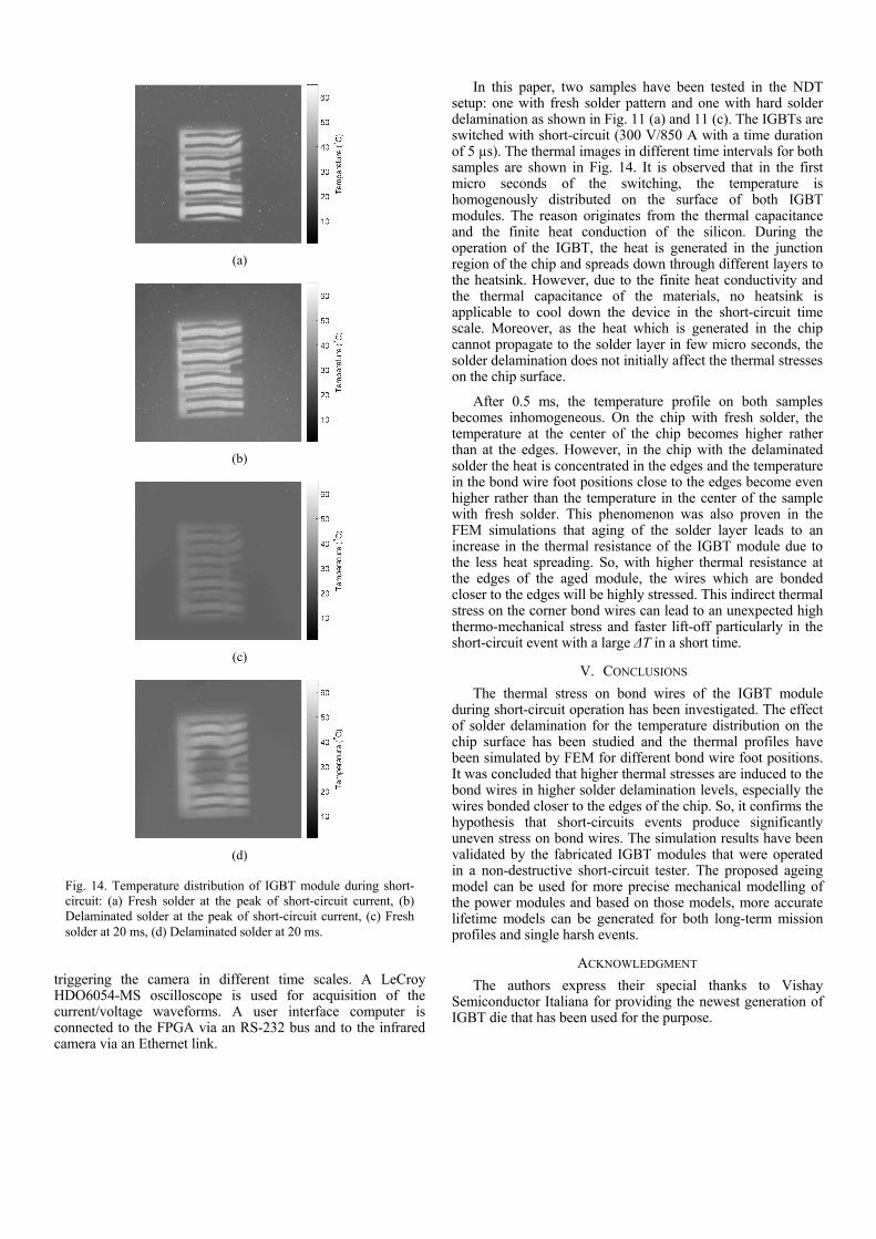
In this paper, two samples have been tested in the NDT setup: one with fresh solder pattern and one with hard solder delamination as shown in Fig. 11 (a) and 11 (c). The IGBTs are switched with short-circuit (300 V/850 A with a time duration of 5 µs). The thermal images in different time intervals for both samples are shown in Fig. 14. It is observed that in the first micro seconds of the switching, the temperature is homogenously distributed on the surface of both IGBT modules. The reason originates from the thermal capacitance and the finite heat conduction of the silicon. During the operation of the IGBT, the heat is generated in the junction region of the chip and spreads down through different layers to the heatsink. However, due to the finite heat conductivity and the thermal capacitance of the materials, no heatsink is applicable to cool down the device in the short-circuit time scale. Moreover, as the heat which is generated in the chip cannot propagate to the solder layer in few micro seconds, the solder delamination does not initially affect the thermal stresses on the chip surface.
After 0.5 ms, the temperature profile on both samples becomes inhomogeneous. On the chip with fresh solder, the temperature at the center of the chip becomes higher rather than at the edges. However, in the chip with the delaminated solder the heat is concentrated in the edges and the temperature in the bond wire foot positions close to the edges become even higher rather than the temperature in the center of the sample with fresh solder. This phenomenon was also proven in the FEM simulations that aging of the solder layer leads to an increase in the thermal resistance of the IGBT module due to the less heat spreading. So, with higher thermal resistance at the edges of the aged module, the wires which are bonded closer to the edges will be highly stressed. This indirect thermal stress on the corner bond wires can lead to an unexpected high thermo-mechanical stress and faster lift-off particularly in the short-circuit event with a large ΔT in a short time.
V. CONCLUSIONS
The thermal stress on bond wires of the IGBT module during short-circuit operation has been investigated. The effect of solder delamination for the temperature distribution on the chip surface has been studied and the thermal profiles have been simulated by FEM for different bond wire foot positions. It was concluded that higher thermal stresses are induced to the bond wires in higher solder delamination levels, especially the wires bonded closer to the edges of the chip. So, it confirms the hypothesis that short-circuits events produce significantly uneven stress on bond wires. The simulation results have been validated by the fabricated IGBT modules that were operated in a non-destructive short-circuit tester. The proposed ageing model can be used for more precise mechanical modelling of the power modules and based on those models, more accurate lifetime models can be generated for both long-term mission profiles and single harsh events.
ACKNOWLEDGMENT
The authors express their special thanks to Vishay Semiconductor Italiana for providing the newest generation of IGBT die that has been used for the purpose.
(a)
(b)
(c)
(d)
Fig. 14. Temperature distribution of IGBT module during short-circuit: (a) Fresh solder at the peak of short-circuit current, (b) Delaminated solder at the peak of short-circuit current, (c) Fresh solder at 20 ms, (d) Delaminated solder at 20 ms.
REFERENCES [1] J. L. Hudgins, “Power electronic devices in the future,” IEEE J. Emerg.
Sel. Topics Power Electron., vol. 1, no. 1, pp. 11–17, Mar. 2013.
[2] F. Blaabjerg and K. Ma, “Future on power electronics for wind turbine systems,” IEEE J. Emerg. Sel. Topics Power Electron., vol. 1, no. 3, pp. 139–152, Sep. 2013.
[3] J. Flicker, R. Kaplar, B. Yang, M. Marinella, and J. Granata, “Insulated gate bipolar transistor reliability testing protocol for PV inverter applications,” Prog. Photovolt., Res. Appl., vol. 22, no. 9, pp. 970–983, Sep. 2014.
[4] Y. Li Yang, P. A. Agyakwa, C. M. Johnson, "Physics-of-Failure Lifetime Prediction Models for Bond wire Interconnects in Power Electronic Modules," IEEE Trans. Device and Materials Reliability, vol.13, no.1, pp. 9-17, March 2013.
[5] S. Yang, A. Bryant, P. Mawby, D. Xiang, L. Ran, and P. Tavner, “An industry-based survey of reliability in power electronic converters,” IEEE Trans. Industry Appl., vol. 47, no. 3, pp. 3151-3157, 2009.
[6] U. M. Choi, F. Blaabjerg, and K. B. Lee, “Study and Handling Methods of Power IGBT Module Failures in Power Electronic Converter Systems,” IEEE Trans. Power Electron., vol. 30, no. 5, pp. 2517-2533, May. 2015.
[7] H. Wang, M. Liserre , F. Blaabjerg , P. Rimmen , J. B. Jacobsen , T. Kvisgaard , J. Landkildehus “Transitioning to physics-of-failure as a reliability driver in power electronics,” IEEE J. Emerg. Sel. Topics Power Electron., vol. 2, no. 1, pp. 97–114, Mar. 2014.
[8] B. Czerny, G. Khatibi, “Interface reliability and lifetime prediction of heavy aluminum bond wires,” Microelectron. Reliab., Vol. 58, pp. 65-72, March 2016.
[9] Y. Li Yang, P. A. Agyakwa, C. M. Johnson, "Physics-of-Failure Lifetime Prediction Models for Bond wire Interconnects in Power Electronic Modules," IEEE Trans. Device and Materials Reliability, vol.13, no.1, pp. 9-17, Mar. 2013.
[10] A. S. Bahman, K. Ma, P. Ghimire, F. Iannuzzo, F. Blaabjerg, "A 3D Lumped Thermal Network Model for Long-term Load Profiles Analysis in High Power IGBT Modules," IEEE J. Emerg. Sel. Topics Power Electron., in press, DOI: 10.1109/JESTPE.2016.2531631, 2016.
[11] F. Dugal, M. Ciappa, “Study of thermal cycling and temperature aging on PbSnAg die attach solder joints for high power modules” Microelectron, Reliab., Vol. 54, pp. 1856-1861, 2014
[12] O. Schilling, M. Schäfer, K. Mainka, M. Thoben, F. Sauerland, “Power cycling testing and FE modelling focussed on Al bond wire fatigue in high power IGBT modules,” Microelectron. Reliab., Vol. 52, pp. 2347-2352, 2012.
[13] K. B. Pedersen, P. K. Kristensen, V. Popok, K. Pedersen, "Degradation Assessment in IGBT Modules Using Four-Point Probing Approach," IEEE Trans. Power Electron., vol.30, no.5, pp. 2405-2412, May 2015.
[14] M. Musallam, Y. Chunyan, C. Bailey, M. Johnson, "Mission Profile-Based Reliability Design and Real-Time Life Consumption Estimation in Power Electronics," IEEE Trans. Power Electron., vol.30, no.5, pp. 2601-2613, May 2015.
[15] J. P. Sommer, T. Licht, H. Berg, K. Appelhoff, B. Michel, "Solder Fatigue at High-Power IGBT Modules," in Proc. of CIPS 2006, pp. 1-6, 2006.
[16] O. Hyunseok, H. Bongtae, P. McCluskey, H. Changwoon, B. D. Youn, "Physics-of-Failure, Condition Monitoring, and Prognostics of Insulated Gate Bipolar Transistor Modules: A Review," IEEE Trans. Power Electron., vol.30, no.5, pp. 2413-2426, May 2015.
[17] J. F. Shackelford and W. Alexander, Materials Science and Engineering Handbook, Ed. James, F. Shackelford & W. Alexander Boca Raton: CRC Press LLC, 2001.
[18] M. Ciappa, “Selected failure mechanisms of modern power modules,” Microelectron. Reliab., vol. 42, no. 4-5, pp. 653-667, Jan. 2002.
[19] A. S. Bahman, F. Iannuzzo, F. Blaabjerg, “Mission-profile-based stress analysis of bond-wires in SiC power modules”, Microelectron. Reliab., in press, 2016.
[20] G. Mitic, R. Beinert, P. Klofac, H.J. Schultz, G. Lefranc, “Reliability of AlN substrates and their solder joints in IGBT power modules, Microelectron. Reliab., Vol. 39, Issue 6, pp. 1159-1164, 1999.
[21] A. Hamidi, N. Beck, K. Thomas, E. Herr, “Reliability and lifetime evaluation of different bond wireing technologies for high power IGBT modules,” Microelectron. Reliab., Vol. 39, Issue 6, pp. 1153-1158, 1999.
[23] B. Nagl, J. Nicolics and W. Gschohsmann, "Analysis of thermomechanically related failures of traction IGBT power modules at short circuit switching," in Proc. of ESTC 2010, pp. 1-6, 2010.
[24] R. Wu, L. Smirnova, F. Iannuzzo, H. Wang and F. Blaabjerg, "Investigation on the short-circuit behavior of an aged IGBT module through a 6 kA/1.1 kV non-destructive testing equipment," in Proc. of IECON 2014 , pp. 3367-3373, 2014.
[25] Mega Electronics, “Dry Film Soldermask,” 500-195-2 datasheet, 2009.
[26] A. S. Bahman, F. Blaabjerg, A. Dutta, A. Mantooth, "Electrical parasitics and thermal modeling for optimized layout design of high power SiC modules," in Proc. of APEC 2016, pp. 3012-3019, 2016.