ABSTRACT Title of Document: SINGLE-EVENT GATE RUPTURE IN POWER MOSFETS: A NEW RADIATION HARDNESS ASSURANCE APPROACH Jean-Marie Lauenstein, Ph.D. Candidate, 2011 Directed By: Professor Neil Goldsman, Department of Electrical and Computer Engineering Almost every space mission uses vertical power metal-semiconductor-oxide field-effect transistors (MOSFETs) in its power-supply circuitry. These devices can fail catastrophically due to single-event gate rupture (SEGR) when exposed to energetic heavy ions. To reduce SEGR failure risk, the off-state operating voltages of the devices are derated based upon radiation tests at heavy-ion accelerator facilities. Testing is very expensive. Even so, data from these tests provide only a limited guide to on-orbit performance. In this work, a device simulation-based method is developed to measure the response to strikes from heavy ions unavailable at accelerator facilities but posing potential risk on orbit. This work is the first to show that the present derating factor, which was established from non-radiation reliability concerns, is appropriate to reduce on-orbit SEGR failure risk when applied to data acquired from ions with appropriate penetration range. A second important outcome of this study is the
Transcript
ABSTRACT
Title of Document: SINGLE-EVENT GATE RUPTURE IN POWER MOSFETS: A NEW RADIATION HARDNESS ASSURANCE APPROACH
Jean-Marie Lauenstein, Ph.D. Candidate, 2011
Directed By: Professor Neil Goldsman, Department of Electrical and Computer Engineering
Almost every space mission uses vertical power metal-semiconductor-oxide
field-effect transistors (MOSFETs) in its power-supply circuitry. These devices can
fail catastrophically due to single-event gate rupture (SEGR) when exposed to
energetic heavy ions. To reduce SEGR failure risk, the off-state operating voltages of
the devices are derated based upon radiation tests at heavy-ion accelerator facilities.
Testing is very expensive. Even so, data from these tests provide only a limited guide
to on-orbit performance.
In this work, a device simulation-based method is developed to measure the
response to strikes from heavy ions unavailable at accelerator facilities but posing
potential risk on orbit. This work is the first to show that the present derating factor,
which was established from non-radiation reliability concerns, is appropriate to
reduce on-orbit SEGR failure risk when applied to data acquired from ions with
appropriate penetration range. A second important outcome of this study is the
demonstration of the capability and usefulness of this simulation technique for
augmenting SEGR data from accelerator beam facilities.
The mechanisms of SEGR are two-fold: the gate oxide is weakened by the
passage of the ion through it, and the charge ionized along the ion track in the silicon
transiently increases the oxide electric field. Most hardness assurance methodologies
consider the latter mechanism only. This work demonstrates through experiment and
simulation that the gate oxide response should not be neglected. In addition, the
premise that the temporary weakening of the oxide due to the ion interaction with it,
as opposed to due to the transient oxide field generated from within the silicon, is
validated. Based upon these findings, a new approach to radiation hardness assurance
for SEGR in power MOSFETs is defined to reduce SEGR risk in space flight
projects.
Finally, the potential impact of accumulated dose over the course of a space
mission on SEGR susceptibility is explored. SEGR evaluation of gamma-irradiated
power MOSFETs suggests a non-significant SEGR susceptibility enhancement due to
accumulated dose from gamma rays. During SEGR testing, an unexpected enhanced
dose effect from heavy-ion irradiation was detected. We demonstrate that this effect
could be due to direct ionization by two or more ions at the same channel location.
The probability on-orbit for such an occurrence is near-zero given the low heavy-ion
fluence over a typical mission lifetime, and did not affect SEGR susceptibility.
The results of this work can be used to bound the risk of SEGR in power
MOSFETs considered for insertion into spacecraft and instruments.
SINGLE-EVENT GATE RUPTURE IN POWER MOSFETS: A NEW RADIATION HARDNESS ASSURANCE APPROACH
By
Jean-Marie Lauenstein
Dissertation submitted to the Faculty of the Graduate School of the University of Maryland, College Park, in partial fulfillment
of the requirements for the degree of Doctor of Philosophy
2011
Advisory Committee: Professor Neil Goldsman, Chair Professor Martin Peckerar Associate Professor Pamela Abshire Professor John Melngailis Professor Aris Christou
First and foremost, I extend my utmost appreciation and thanks to my advisor,
Professor Neil Goldsman, for his support, guidance, instruction, friendship, and
device-physics intuition. He led me into the deep, carrying the lantern to show me
the way.
I am thankful to my dissertation committee members, Professors Pamela
Abshire, Martin Peckerar, John Melngailis, and Aris Christou, for their time and
service.
This work was supported in part by the National Aeronautics and Space
Administration’s (NASA) Electronic Parts and Packaging Program, NASA Flight
Projects, the Defense Threat Reduction Agency under IACRO10-4977I, and the
NASA Goddard Space Flight Center Internal Research and Development Program.
This work was conducted in part using the resources of the Department of Electrical
and Computer Engineering at the University of Maryland, College Park, MD,
CoolCAD Electronics, College Park, MD, the Advanced Computing Center for
Research and Education at Vanderbilt University, Nashville, TN, and International
Rectifier Corporation, El Segundo, CA.
Special thanks for helpful technical discussions with and encouragement from
Raymond L. Ladbury, Sandra Liu, Max Zafrani, Jeffrey L. Titus, Kenneth A. LaBel,
Akin Akturk, Siddarth Potbhare, Jack Shue, Leif Z. Scheick, Timothy Oldham,
Michael Xapsos, Christian Poivey, Fredrik Sturesson, Véronique Ferlet-Cavrois,
iv
Robert A. Reed, Robert A. Weller, Ron Schrimpf, Kenneth F. Galloway, and Art F.
Witulski.
Assistance with experimental testing from Hak S. Kim and Anthony M. Phan is
gratefully acknowledged. Thank you to Ken LaBel for providing the latitude and
support to conduct these experiments. Technical assistance from Stephen Cox,
Timothy Irwin, Donald Hawkins, Martha O’Bryan, Donna Cochran, Stephen Brown,
Tom Ward, and Yevgeniy Gerashchenko is also acknowledged and appreciated.
Sometimes in our life, we are fortunate to find ourselves surrounded by
individuals who take on an unspoken role of mentor to us. I am blessed to have been
shepherded first into the radiation environment community by Janet Barth, then the
radiation effects community by Ray Ladbury and the power MOSFET world by Jack
Shue. I am particularly thankful for Ray’s open door, through which he never tired of
me entering at times seemingly daily.
Finally, my friends and family formed a tremendous support system through
this process. I am particularly grateful to Sue Kovalsky, Roxanne Corrado, Dee
Thorne, and Heather Podesek, who together rose to become extended family in their
unwavering care week in and week out.
v
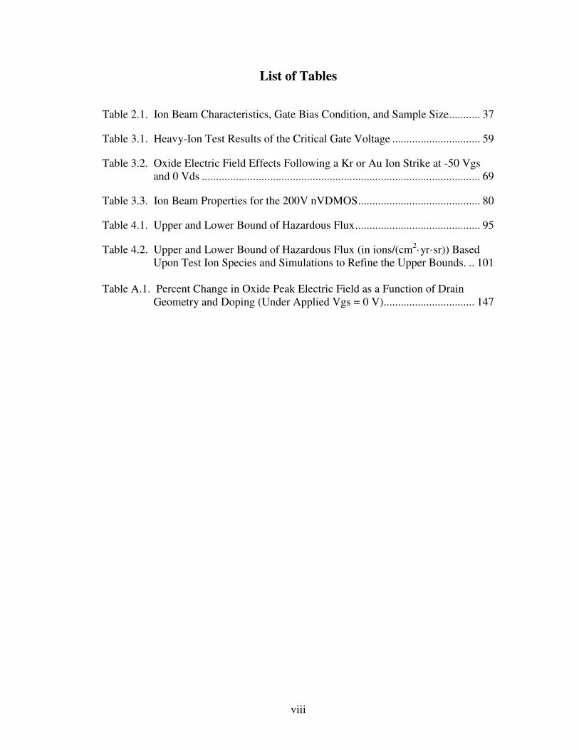
Table of Contents
Dedication ii Acknowledgments....................................................................................................... iii Table of Contents ......................................................................................................... v
List of Tables ............................................................................................................ viii List of Figures ............................................................................................................. ix
1.6 Deficiencies in Methodologies for Evaluating and Mitigating SEGR Susceptibility in Power MOSFETs ................................................................. 23
1.6.1 Limitations of Heavy-Ion Testing ............................................................. 23
1.6.2 Deficiencies of the LET Metric ................................................................ 26
Chapter 3: Studies of Ion Species Effects in SEGR Susceptibility of Power MOSFETs ................................................................................................ 54
3.2 Verification of the Titus-Wheatley Formula of the Critical Oxide Electric Field for SEGR ............................................................................................... 55
3.2.3 Implication for Simulation Methods of SEGR Prediction ........................ 61
3.3 Validation of the Experimental Method to Isolate the Critical Oxide Field for Gate Rupture ................................................................................................... 62
3.4 Two-Photon Absorption Laser Tests to Reveal the Criticality of Gate-Oxide Damage for SEGR .......................................................................................... 71
3.4.5 Next Steps ................................................................................................. 77
3.5 Relative Roles of Heavy-Ion Interactions with the Oxide, Epilayer, and Substrate .......................................................................................................... 77
3.5.3 Discussion and Implication for SEGR Hardness Assurance in Power MOSFETs ................................................................................................. 85
Chapter 4: A New Hardness Assurance Approach for Bounding the On-Orbit Risk of SEGR .................................................................................................. 90
4.1 Applying the SEE Response Curve to the Two-Dimensional Heavy-Ion Environment for a Space Mission ................................................................... 90
4.2 Applying SEGR Simulation Methods to Narrow the Bounds of the Hazardous Flux ................................................................................................................. 99
4.3 Proposed Methods for Further Refinement of the Upper Bound of Hazardous Flux ............................................................................................................... 102
4.4 Step-by-Step: The New SEGR Hardness Assurance Approach Summarized ... ....................................................................................................................... 103
Chapter 5: Improvement of Our Understanding of How Accumulated Dose Affects SEGR Susceptibility .............................................................................. 107
Chapter 6: Conclusion and Future Work ................................................................ 134
6.1 Accomplishments of this Research ............................................................... 134
6.2 Discussion of the Role of the Ion Species in SEGR ..................................... 137
6.3 Future Work .................................................................................................. 142
6.3.1 Determination of the Angle-Dependence on the Oxide Response to Heavy-Ion Strikes, and Subsequent Angular-Response Mapping of SEGR Susceptibility........................................................................................... 142
6.3.2 Enhancement of Our Understanding of the Oxide Damage Mechanisms Important for SEGR ................................................................................ 143
Appendix A ............................................................................................................... 146
Table 2.1. Ion Beam Characteristics, Gate Bias Condition, and Sample Size ........... 37
Table 3.1. Heavy-Ion Test Results of the Critical Gate Voltage ............................... 59
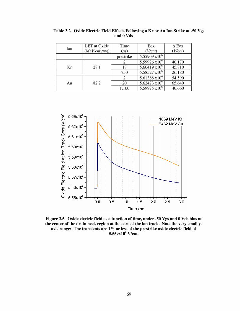
Table 3.2. Oxide Electric Field Effects Following a Kr or Au Ion Strike at -50 Vgs and 0 Vds .................................................................................................. 69
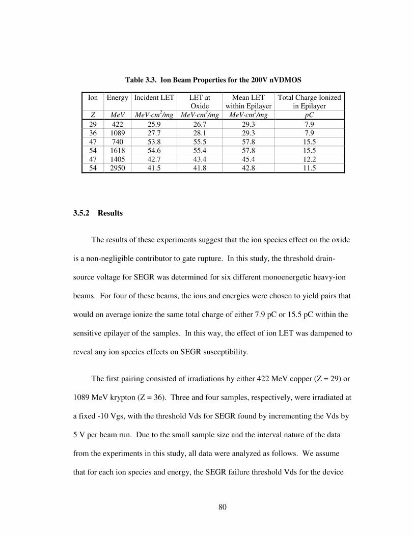
Table 3.3. Ion Beam Properties for the 200V nVDMOS ........................................... 80
Table 4.1. Upper and Lower Bound of Hazardous Flux ............................................ 95
Table 4.2. Upper and Lower Bound of Hazardous Flux (in ions/(cm2·yr·sr)) Based Upon Test Ion Species and Simulations to Refine the Upper Bounds. .. 101
Table A.1. Percent Change in Oxide Peak Electric Field as a Function of Drain Geometry and Doping (Under Applied Vgs = 0 V) ................................ 147
ix
List of Figures
Figure 1.1. Illustration of a n-type VDMOSFET. ........................................................ 2
Figure 1.2. Stripe (left) and HEXFET® (right) cell topologies with gate (G) and source (S) regions labeled. ............................................................................................ 2
Figure 1.3. The space radiation environment ............................................................... 5
Figure 1.4 Illustration showing device response to an ion strike to the drain neck region. ......................................................................................................................... 17
Figure 1.5. Integral Flux vs. LET for various orbits during solar minimum with 100 mils Al shielding ......................................................................................................... 21
Figure 2.1. Ion LET as a function of penetration depth into silicon .......................... 36
Figure 2.2. A: Flowchart depicting test procedure, after [42]; ................................. 38
Figure 2.3. Single-event effect response curves for the 200V nVDMOS showing energy dependence at the higher LET ........................................................................ 41
Figure 2.7. Simulated SEGR threshold Vds as a function of Vgs for Au ions versus SOAs defined from derating the 200V nVDMOS test data. ....................................... 47
Figure 2.8. Single-event effect response curves for the 500V pVDMOS showing ... 48
Figure 2.9. Simulated SEGR threshold Vds as a function of Vgs for simulated Au ion strikes versus 0.75 derating factor applied to test and simulated SEE response curves for the 500V pVDMOS ............................................................................................... 49
Figure 3.1. A: Flowchart depicting test procedure, after [42]. B: Test circuit diagram. C. TAMU operator control room with test equipment. D. Test board with DUT in line with beam. .............................................................................................. 57
Figure 3.2. Critical Vgs for SEGR as a function of ion species. ............................... 61
x
Figure 3.3. Electric field in the gate oxide and silicon epilayer beneath prior to a Au-ion strike (left) and at 20 ps following the strike (right) – the time at which the maximum change in the oxide field occurred. ............................................................ 65
Figure 3.4 (on following pages). Effects of Au ion strike at 0 Vds and -50 Vgs on: A. Electric field; B-C. Electrostatic potential; D. Electron density; and E. Hole density. Time elapsed: 1) prestrike; 2) 2 ps; 3) 20 ps (time of maximum transient electric field); 4) 1 ns. .............................................................................................................. 65
Figure 3.5. Oxide electric field as a function of time, under -50 Vgs and 0 Vds bias at the center of the drain neck region at the core of the ion track ................................... 69
Figure 3.6. Sample prepared for backside TPA laser testing. Top: Frontside showing the die wire-bonded to the package. Bottom: Backside showing drilled window in the package to expose the well-polished back surface of the drain substrate. ..................................................................................................................... 73
Figure 3.7. Laser test board with sample mounted (top). Board is placed on a stage beneath a 100X microscope objective used to focus the laser beam. Circuit diagram for the test board is shown at the bottom. ................................................................... 74
Figure 3.8. Ion LET as a function of penetration depth. Vertical dashed lines demarcate the epilayer region. .................................................................................... 79
Figure 3.9. SEGR response curve for Cu versus Kr irradiation. ................................ 82
Figure 3.10. SEGR response curve for silver versus xenon, at incident LETs of 54 MeV·cm2/mg............................................................................................................... 83
Figure 3.11. SEGR response curves for 1405 MeV silver versus 2950 MeV xenon ions. ............................................................................................................................. 84
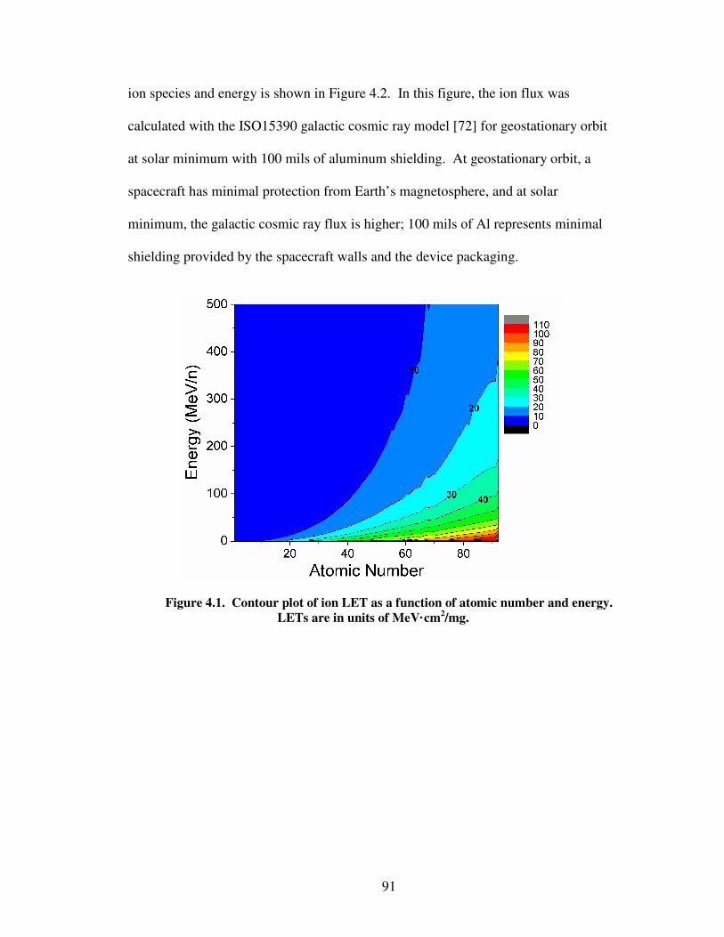
Figure 4.1. Contour plot of ion LET as a function of atomic number and energy. LETs are in units of MeV·cm2/mg.............................................................................. 91
Figure 4.2. Heavy-ion flux at geostationary orbit as a function of ion species and energy. ......................................................................................................................... 92
Figure 4.3A-C (next page). A portion of the heavy-ion spectrum showing the hardness assurance provided by derating the SEE response curve for Br (A), Ag (B), or Au (C). .................................................................................................................... 93
Figure 4.4. Reverse-integral flux over both ion atomic number and LET, at geostationary orbit during solar minimum behind 100 mils Al shielding. ................. 97
Figure 4.5. Upper bound of hazardous flux (per steradian of vulnerability) at geostationary orbit during solar minimum behind 100 mils Al shielding, as a function of test ion species and incident LET. Panel A shows the solution to (9); panel B
xi
shows the final result after removing non-physical combinations of ion species and LETs. ........................................................................................................................... 98
Figure 4.6. Refined upper bound of hazardous flux (per steradian of vulnerability) at geostationary orbit during solar minimum behind 100 mils Al shielding, as a function of test ion species and incident LET. ........................................................................ 101
Figure 5.1. Bias circuit during gamma-irradiation of the 500V nVDMOS samples.................................................................................................................................... 114
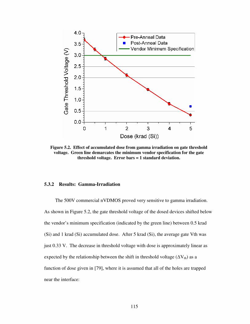
Figure 5.2. Effect of accumulated dose from gamma irradiation on gate threshold voltage ....................................................................................................................... 115
Figure 5.3. Subthreshold IV curves as a function of total accumulated dose .......... 118
Figure 5.4. Total gate threshold voltage shift as a function of dose (Vth, red line) is a sum of the shift due to oxide trapped charge (Vot, blue line) and interface trapped charge (Vit, green line). ............................................................................................ 119
Figure 5.5. Two samples mounted on the test board ready in turn to be aligned in the ion beam. ................................................................................................................... 121
Figure 5.6. Mean threshold drain-source voltage (Vds) at which gate rupture occurred, as a function of prior accumulated dose from gamma rays ...................... 123
Figure 5.7. Pristine sample failure threshold Vds versus dosed sample threshold Vds. Blue and red columns reflect the range of failure Vds values within the 90% CL. .. 123
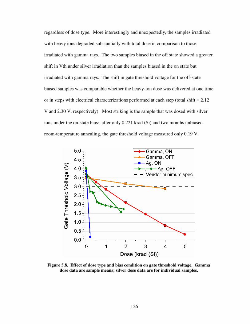
Figure 5.8. Effect of dose type and bias condition on gate threshold voltage ......... 126
Figure 5.9. IV curves showing the different characteristics in the subthreshold current introduced by silver ion irradiation versus gamma irradiation. ................................ 128
Figure A.0.1. Breakdown voltage curves showing the effect of increased epilayer doping. ...................................................................................................................... 148
1
Chapter 1: Introduction
1.1 Importance of Power MOSFETs in Space Missions
Power metal-oxide-semiconductor field-effect transistors (MOSFETs) were
developed in the 1970s to enable high-speed switching, simpler drive circuitry, and
the handling of power spikes in inductive switching circuits [1]. These devices most
commonly have a vertical structure (Figure 1.1) in which current flows out of the
drain substrate region upward through the drain epitaxial region, then laterally across
the channel to the source. This structure permits blocking of high drain-source
voltages by providing a large depletion region in the epitaxial layer when biased in
the off state. The doping and thickness of this epitaxial layer determine the
breakdown voltage of the device. Typical values may include 3x10¹⁵ ions/cm3 and 15
µm for a 100V device, 1x10¹⁵ ions/cm3 and 26 µm for a 200 V device, and 4x10¹⁴
ions/cm3 and 40 µm for a 400 V device [2, 3]. Power MOSFETs typically have high
gate bias ratings of ±20V, necessitating a gate oxide thickness of approximately 100
nm. The channel length is determined by the width of diffused body region relative
to that of the source region, and typically measures 1 µm – 2 µm [4]. This process is
therefore referred to as a vertical double-diffused power MOSFET (VDMOS). To
achieve high currents, thousands to millions of cells are placed in parallel in either a
hexagonal configuration or a striped configuration (Figure 1.2); single-cell stripline
geometries also exist.
2
Figure 1.1. Illustration of a n-type VDMOSFET. The drain region comprises both the
highly-doped substrate region (blue, near the bottom of the structure) and the lightly-
doped epilayer region (white). Current flows upward from the drain substrate, across
the channels (labeled) and out the highly-doped sources (blue, near the top of the
structure). Modified with permission from: International Rectifier Corporation
Application Note AN1084.
Figure 1.2. Stripe (left) and HEXFET® (right) cell topologies with gate (G) and source
(S) regions labeled. From [5]; reprinted with permission.
The benefits of power MOSFETs afforded over other power devices have made
their use in space missions ubiquitous. Spacecraft components commonly relying on
power MOSFETs include power supply electronics where the MOSFETs serve as
3
shunt regulators to maintain steady bus voltages; battery charge assemblies where
they serve as part of buck or boost converters; momentum wheel assemblies for
spacecraft attitude control where they serve as power switches; and power converters
in which they serve as choppers to provide appropriate DC voltages to the payload
and spacecraft circuitry [6, 7]. Power MOSFETs perform many vital functions within
a single mission, making their reliability within the harsh space radiation environment
essential to mission success.
The heavy-ion environment in space poses a risk of a potentially catastrophic
failure of the gate dielectric, known as single-event gate rupture (SEGR). This
research seeks to evaluate and refine current methods for estimating and reducing
SEGR risk in space flight projects. As part of this effort, the relative importance of
the mechanisms contributing to SEGR is revealed through experiment and simulation.
In this introductory chapter, an overview of the space radiation environment and its
effects on microelectronics is provided. In addition, SEGR failure mechanisms and
the methods commonly used to mitigate SEGR are presented.
1.2 Overview of the Space Radiation Environment
All of the natural elements of the periodic table occur in space as energetic ions.
Together with electrons and high-energy photons, these protons, helium ions, and
other heavier ions compose the space radiation environment. These particles
originate from the sun during solar particle events, and from outside the solar system
as galactic cosmic rays thought to stem in part from supernova explosions [8]. Some
of these particles become trapped in planetary magnetic fields, forming radiation belts
4
that vary in composition and flux over time and location within the planetary
magnetosphere. These transient and trapped particles may contribute to power
MOSFET performance degradation over time; furthermore, the transient heavier ions
can cause irreversible catastrophic failure of these devices. It is therefore important
to understand the environment in which these devices will be used to evaluate the
probabilities of these radiation effects during the mission lifetime.
The solar wind, a plasma consisting of protons, electrons, and other ionized
gases, flows out from the sun continuously at speeds upwards to a million miles per
hour [9]. The solar wind interacts with Earth’s magnetic field, compressing it on the
sunward side and preventing closure of field lines from Earth’s polar caps, sweeping
them into a tail that may extend more than 1000 Earth-radii into the night-side [9]
(Figure 1.3). Within 4-5 Earth-radii, Earth’s magnetic field remains fairly dipolar
[10], and can trap or deflect solar and galactic energetic particles.
5
Figure 1.3. The space radiation environment. Solar wind shapes Earth’s magnetic field
lines. After: Nikkei Science, Inc. of Japan, by K. Endo.
Solar particle events include solar flares which are electron-rich events lasting
on the scale of hours, and coronal mass ejections (CMEs) which are days-long
eruptions of proton-rich plasma accelerated to energies as high as GeVs/nucleon [8,
10]. Although ions heavier than helium form only about 0.1% of the composition of
CMEs, these are the particles likely to cause destructive failures in power MOSFETs.
In addition, the composition of galactic cosmic rays (GCRs) includes about 1% of
ions heavier than helium and can have energies as high as 1011 GeV, with peak
energies of about 1 GeV ner nucleon [8, 9]. These high energies render shielding
ineffective in protecting the power MOSFET from GCRs.
6
Earth’s inner magnetic field provides protection from many of the solar and
GCR charged particles by deflecting or trapping them according to the Lorentz Force
Law (1).
)( BvEF ×+= q (1)
The trapped particle gyrates around the field line, bouncing between poles due
to the convergence of magnetic field lines at the poles. Within the radius of gyration,
the magnetic field is stronger closer to Earth; the particles therefore slowly drift either
eastward (electrons) or westward (protons and positive ions) around Earth. This
motion forms the inner belt of protons and an electron belt having both inner and
outer zones. The trapped particles have energies varying from less than 1 keV up to
hundreds of MeV. If the solar or galactic cosmic ray particles have enough
momentum, they can penetrate through the magnetic field, reaching even low-altitude
spacecraft electronics. In addition, at the polar regions of Earth, the geomagnetic
field lines are more perpendicular to the surface of Earth, resulting in even lower-
energy particles penetrating deeper toward Earth as they follow the field lines. Figure
4 shows the flux versus linear energy transfer (LET – the electronic stopping power,
dE/dx, normalized to the material density) spectrum for several different Earth orbits,
demonstrating the protective nature of the geomagnetic field. A more detailed
description of the trapped radiation environment may be found in [8-11] and
references therein.
The cyclical activity of the sun impacts the radiation hazard to power
MOSFETs and other electronics by contributing to and modulating the radiation
7
environment. The level of solar activity varies on a cycle of an approximately 11
years, which also correleates roughly with the number of sun spots [9]. More
frequent and intense solar particle events occur during the decline of the 7-year solar
sunspot maximum, with quieter activity marking the 4-year solar minimum. The
cycle of activity modulates the galactic cosmic ray and trapped radiation fluxes.
During the period of solar maximum, the proton belt experiences losses from
increased collisions with Earth’s atmosphere which heats and expands in altitude.
This loss mechanism is beneficial for power MOSFETs flying in low Earth orbits
because at these low altitudes, protons are the primary source of total ionizing dose
degradation of electrical characteristics such as the gate threshold voltage and drain-
source breakdown voltage. At higher Earth orbits, the electron contribution to this
degradation increases during solar maximum due to solar activity being the key
source of electrons.
The solar wind provides some attenuation to the flux of galactic cosmic rays:
during solar maximum, the more intense solar wind and solar magnetic field help to
deflect galactic cosmic rays according to (1), decreasing the near-Earth flux of
particles with energies below 10 GeV/nucleon as compared to solar minimum levels
[8]. Due to the higher energies of the galactic cosmic rays as compared to solar
particles, the less-protective solar minimum period can therefore be worse for
destructive failures in power MOSFETs despite the reduction in solar particle events.
Finally, although the frequency and intensity of solar particle events is greater during
the declining phase of solar maximum, a significant solar particle event may occur at
any time in the cycle. The resulting solar wind turbulence can further compress the
8
geomagnetic field, temporarily removing its ion-deflecting protection from higher-
orbiting spacecraft, and increasing exposure of low-Earth orbit spacecraft to the
trapped radiation belts [12].
1.3 Summary of Radiation Effects on Microelectronics
The space radiation environment can damage microelectronic components in
both an immediate and a cumulative fashion. The accumulation of dose during the
course of the mission may result in performance degradation over time; the devices
must therefore be evaluated to ensure that they will perform adequately over the
entire lifetime of the mission. Conversely, component errors or failures may occur
almost instantly upon a strike from a single energetic ion – a single-event effect.
These errors or failures must be mitigated at the device, circuit, or system level. Both
total dose and single-event effects necessitate careful evaluation of each component
selected for use in the spacecraft electronics in order to prevent either costly
overdesign or unexpected risk to the mission success. Power MOSFETs are
particularly susceptible to total ionizing dose effects (due to their thick dielectrics)
and both transient and catastrophic single event effects.
1.3.1 Total Dose
Dose is defined as the amount of energy deposited per unit mass of material.
Photons, electrons, and ions all deposit energy in a device when incident upon it.
Most of the energy loss to space electronics is in the form of ionizing energy loss in
which electron-hole pairs are formed along the track of the particle or photon. A
much smaller portion of the energy loss occurs in the form of displacement damage,
9
in which a collision (or coulombic interaction) displaces a lattice atom, forming an
interstitial atom and a vacancy referred to as a Frenkel defect or pair [13, 14]. If the
initially displaced recoil atom has enough energy, it too can displace other atoms,
resulting in a cluster or a tree of clusters of defects. These defects may be electrically
active, forming traps or generation-recombination centers that decrease minority-
carrier lifetime and majority-carrier density and mobility [15]. Trapping centers near
the intrinsic Fermi level can result in increased leakage current in reverse-biased p-n
junctions [14]. Displacement damage is more important in bipolar devices; although
in MOS devices such as power MOSFETs, damage to the silicon can degrade charge
mobility, and displacement damage in the gate oxide may play a role in single-event
gate rupture [16].
In contrast, degradation of MOSFETs by ionizing radiation occurs as a result of
charge buildup in the dielectrics. The passage of radiation through the dielectric
generates electron-hole pairs. The number of pairs produced per unit dose can be
determined from the material density and energy required to create an electron-hole
pair for that material [17]. The unit commonly used in space radiation physics is the
rad, an abbreviation for radiation absorbed dose. One rad equals 6.25x10¹³ eV of
absorbed radiation energy per gram of material; this unit is therefore material
dependent, requiring that the material always be indicated with the unit (e.g., rad
(Si)).
Irradiation of the gate oxide initiates a series of events resulting in trapped
charges that impact the device gate threshold voltage. The initial density of electron-
hole pair formation is determined by the electronic stopping power, or linear energy
10
transfer (LET) of the material for the incident particle and thus varies depending on
incident particle type and energy [18]. Depending on the strength of the electric field
in the oxide and on the density of pair formation, a number of electron-hole pairs will
recombine within a picosecond via columnar or geminate recombination mechanisms
[19, 20]. Because the electron mobility in silicon dioxide is much greater than that of
holes, a gate bias transports the free electrons out of the oxide within picoseconds
[21]. A charge imbalance thus develops due to the remaining holes that survived
initial recombination. This imbalance causes an initial negative shift in the threshold
voltage [12].
In n-type MOS devices, the presence of a positive gate bias causes the holes in
the oxide to move toward the Si/SiO2 interface. The motion is highly temperature
dependent [21] and is characterized by polaron hopping [18]. A polaron is the
combination of a hole or electron and its strain field (the distortion of the lattice due
to the coulombic interaction with the charge carrier); the lattice distortion from the
hole results in a self-trapping [22]. The time to reach the interface varies as the fourth
power of the thickness of the oxide (tox4), and is due to a phenomenon whereby the
further a hole travels, the greater the chance that it enters a state from which it is
harder to leave [18].
As the holes near the interface, there is an increased likelihood of becoming
deeply trapped due to the greater density of oxygen vacancies (Si-Si bonds) near the
interface [13]. These trapped holes can anneal out over long time periods: they can
be neutralized by thermally excited electrons promoted from the valence band of the
oxide [12]. Alternatively, holes trapped close to the interface can be neutralized by
11
tunneling electrons from the silicon. The hole remains trapped but is neutralized by
an electron added to the adjacent neutral Si atom, forming a dipole with the hole [18].
The final effect of radiation on the gate oxide is the formation of interface traps.
These are composed of a Si atom bound to three other Si atoms, with the fourth bond
dangling into the oxide to form an amphoteric defect [23]. These traps form slowly
compared with the bulk oxide traps; they are charged positively or negatively
depending on their location with respect to the intrinsic Fermi level. In n-type
MOSFETs, they are primarily negatively charged, but change as the energy bands
bend depending upon the applied bias [24]. Because interface traps do not anneal out
at room temperature, they persist even as the oxide traps slowly neutralize; they
therefore can accumulate over the duration of the space mission [23]. The
mechanism by which radiation forms interface traps is controversial; a discussion can
be found in [23] and is generally described here: Given a Si atom at the interface
bound to three other Si atoms and a hydrogen atom, this bond to the hydrogen atom
gets broken by either the hole or another hydrogen ion freed during the hole transport
through the oxide (in this latter case, the freed hydrogen ion breaks the bond to form
Comparison of these bounds based upon Br, Ag, or Au SEGR data shows that
the heavier the ion used to define a SEE response curve and hence the safe-operating
area for the device, the lower the hazardous flux and the narrower the range between
upper and lower bounds. If LET were the only metric used to identify on-orbit risk,
the potentially hazardous flux would be 1.40x10⁻³ ions/(cm2·yr·sr), the integral flux
96
for all species with LET ≥ 40 MeV·cm2/mg. Table 4.1 suggests that this value would
under-predict the true geosynchronous-orbit hazard.
Following this example, the following algorithm defines the upper bound of
potentially hazardous flux (ФUB) when biasing a device at the limit of the safe
operating area defined by a given ion species, Zi, having a given mission LET
requirement, LETi:
.dLETdZ)LET,Z(dLETdZ)LET,Z( )LET ,(Z 921
119
iLET92
1iZiLET
0iiUB ∫ ∫ ∫ ∫+=Φ∆+ +
φφ (9)
The first term in (9) captures all flux of ions with energies yielding LETs above the
mission LET requirement (this integral encompasses the known hazardous flux and
the portion of unknown hazardous flux in which the species is lighter than the test
ion, but has a higher LET). The second term includes the unknown hazardous flux in
which the ion species is heavier than the test ion, but the LET is less than the mission
LET requirement (and hence less than the test LET). Note that for now, we do not
make any assumptions about the lower limit of the hazardous LET for these heavier
ion species.
In Figure 4.4, we re-plot the differential flux of ions at geostationary orbit
shown in Figure 4.2 as the reverse-integral flux as a function of ion species and LET.
In this plot (Figure 4.4), the flux has been reverse-integrated over both ion species
and LET, such that for any given species and LET, the flux shown is the total flux for
97
that atomic number and LET plus that of all higher atomic numbers and LETs1. From
this reverse-integral flux plot, it is then easy to extract the upper bounds of hazardous
flux for any combination of test ion species and LET; we show the resulting initial
plot of upper bounds in Figure 4.5A. Figure 4.5A includes non-physical
combinations of species and LETs, that is, the upper bound of hazardous flux for ion
species at LETs higher than are physically possible. We eliminate these
combinations, and our final solution of (9) is the plot in Figure 4.5B. In Figure 4.5B,
we have labeled the points corresponding to the ion species (Br, Ag, and Au) used in
our example above for a mission LET requirement of 40 MeV·cm2/mg (see Figure
4.3 and Table 4.1).
Figure 4.4. Reverse-integral flux over both ion atomic number and LET, at
geostationary orbit during solar minimum behind 100 mils Al shielding.
1 To calculate the reverse-integral flux over both Z and LET, we have worked with the output of the ISO15390 galactic cosmic ray model and the SRIM-based LET spectrum calculation within the OMERE v.3.4.6.1 software package [64].
98
A.
B.
Figure 4.5. Upper bound of hazardous flux (per steradian of vulnerability) at
geostationary orbit during solar minimum behind 100 mils Al shielding, as a function of
test ion species and incident LET. Panel A shows the solution to (9); panel B shows the
final result after removing non-physical combinations of ion species and LETs.
99
Further refinement of (9) and hence a reduction of the upper bound of hazardous
flux would require more detailed studies to identify the relative importance of ion
species versus energy deposition, as well as the angular response, for the specific
device under consideration. We have already incorporated our knowledge from
chapter 3 suggesting that for comparable energy deposition in the epilayer, the
heavier ion will induce SEGR at a lower threshold bias; this incorporation led to
regions of unknown risk in the flux vs. Z vs. energy (or LET) matrix describing the
space environment. We now adapt the simulation methods we developed in chapter 2
to reduce the amount of flux that composes this unknown risk by examining for what
incident LET a heavier ion will have the same SEGR threshold as a lighter 40
MeV·cm2/mg TAMU test ion. Such a determination cannot be made at accelerator
facilities commonly used for single-event effect evaluation because a heavier ion such
as gold would require acceleration to 100 – 200 MeV/u!
4.2 Applying SEGR Simulation Methods to Narrow the Bounds of the Hazardous
Flux
We refine the upper bound of hazardous flux using the methods developed in
chapter 2. Recall that in chapter 2, we extracted the geometry and doping profile of a
power MOSFET from a small set of test data, and successfully developed a predictive
SEGR response model of the device. We demonstrated how such models could be
used to obtain additional SEGR data without performing further expensive accelerator
beam tests. For the 500 V p-type power MOSFET examined in chapter 2, we have
100
both simulated and experimental data defining a SEE response curve for 21 MeV/n
xenon with an incident LET near 40 MeV·cm2/mg (Figure 2.8). We now wish to
identify the maximum energy a heavier ion can deposit before causing SEGR when
the device is biased on this SEE response curve for xenon; i.e., the energy at which
that heavier ion would yield the same SEE response as that of xenon, for a particular
Vgs. Toward this end, we simulate gold ion strikes of various energies while biasing
the model at 0 Vgs and -100 Vds. This bias was the highest magnitude before SEGR
occurred under xenon irradiation. We find that a simulated gold ion strike having an
incident LET of 25 MeV·cm2/mg results in SEGR, but that simulations for an
incident LET of 20 MeV·cm2/mg show a transient maximum oxide electric field
below that required for SEGR.
We repeat this simulation experiment in the 200 V nVDMOS model, setting the
bias at 0 Vgs and 100 Vds, the simulated threshold for SEGR under 40 MeV·cm2/mg
silver irradiation (Figure 2.6). Again, we find that at 25 MeV·cm2/mg, the gold ion
induces a transient maximum oxide electric field just greater than that required for
SEGR, but that at 20 MeV·cm2/mg, no SEGR occurs. In both devices, we therefore
find that for LETs at or below half our test ion LET, gold ions (Z=79) will not cause
SEGR when the device is biased at the maximum safe Vds determined by our test ion.
We can thus incorporate our SEGR simulation methodology with our method
for defining the heavy-ion hazardous environment for a power MOSFET under
consideration for a space mission. As an initial conservative reduction of the upper
bound of hazardous flux, we assume that for any given test species and LET, only
those heavier species having LETs greater than half the test LET may pose a hazard.
101
We therefore raise the lower limit of integration over LET in the second term of (9)
from 0 to ½ LETi. The result of this refinement of the upper bound of hazardous flux
is shown in Figure 4.6.
Figure 4.6. Refined upper bound of hazardous flux (per steradian of
vulnerability) at geostationary orbit during solar minimum behind 100 mils Al
shielding, as a function of test ion species and incident LET.
As an example, for both the 500 V commercial pVDMOS and the radiation-
hardened 200 V nVDMOS, the risk of SEGR when biased at 0 Vgs and a Vds within
the safe-operating area for a mission LET requirement of 40 MeV·cm2/mg would
now be bounded according to the hazardous flux values given in Table 4.2.
Table 4.2. Upper and Lower Bound of Hazardous Flux (in ions/(cm2·yr·sr)) Based
Upon Test Ion Species and Simulations to Refine the Upper Bounds.
simulators solve the Poisson, charge-continuity, and current equations in the silicon
using finite-element techniques. In the absence of detailed geometry and doping
profile information, it becomes important to understand how modifications to these
properties affect the model calibration to experimental SEGR data. A brief analysis
of the impact of adjustments to the drain neck width or epilayer doping concentration
is provided here for the 500V pVDMOS model presented in Chapter 2. Simulations
of SEGR were performed using Synopsys Sentaurus Device [59].
Table A.1 demonstrates the effects of changes to the drain neck width and
epilayer doping on the transient peak electric field across the oxide. In this table, the
values of the peak field resulting from krypton, xenon, or gold ion strikes are shown
for the calibrated 500V pVDMOS model. The total drain neck width is then
narrowed by 2 µm, or widened by 2 µm or 4 µm, and the percent change in the peak
electric field across the oxide is noted for each ion. Similarly, the epilayer doping
concentration is increased or decreased from the calibrated model value by about
30%. In each case, the simulations were run under 0 Vgs and the Vds at which SEGR
occurred for the given ion species and energy (see Figures 2.8 and 2.9 in Chapter 2).
Changes in the drain neck width have a greater impact on the oxide transient
electric field than do adjustments to the epilayer doping. As reported previously [46],
a narrower drain neck region results in a lower peak electric field forming across the
oxide. Of the three ions simulated, the transient field resulting from krypton is most
147
sensitive to changes in the drain neck width. Experimentally, samples irradiated with
krypton showed greater part-to-part variability of the threshold drain voltage at which
SEGR occurred [60], suggesting that the lower LET (and hence less charge ionization
in the epilayer) may be responsible for this sensitivity. Simulations in this study
demonstrated a weaker relationship between Vds and the peak transient field across
the oxide for 22 MeV/u krypton than for 21 MeV/u xenon or higher-energy gold.
Significant adjustments to the epilayer doping concentration had only a small
effect on the peak transient electric field. In contrast, these adjustments strongly
affect the drain-source breakdown voltage (BVdss). As plotted in Figure A.1, the
higher doping concentration shown in Table A.1 reduced the breakdown voltage to
below the rated 500 V. Actual devices are designed to break down along the die
edges in the field termination region before breakdown occurs within a cell, whereas
simulated breakdown occurs within the single cell modeled. The epilayer doping
profile therefore should be adjusted to slightly exceed the measured BVdss of the
tested device. The softer simulated breakdown curve results from increasing thermal
charge generation (Shockley-Read-Hall generation) within the cell as the depletion
region expands with increasing reverse drain-source bias.
Table A.1. Percent Change in Oxide Peak Electric Field as a Function of Drain
Geometry and Doping (Under Applied Vgs = 0 V)
Neck Width Epilayer Doping
Ion Vds (V)
Baseline Eox (V/cm)
-2 µm (%)
+2 µm (%)
+4 µm (%)
-1x10¹⁴ /cm3 (%)
+1x10¹⁴ /cm3
(%)
Kr -450 5.3 x 10⁶ -15.9 12.5 20.4 -1.0 1.1 Xe -95 4.3 x 10⁶ -15.1 7.4 10.7 -0.1 5.6 Au -70 3.6 x 10⁶ -13.8 7.1 9.8 -0.9 -0.1
148
Figure A.0.1. Breakdown voltage curves showing the effect of increased epilayer
doping. Actual device breakdown curve (black curve) is shown for comparison to the
models.
149
Bibliography
[1] B. J. Baliga, Power semiconductor devices. Boston: PWS Pub. Co., 1996.
[2] L. E. Selva, G. M. Swift, W. A. Taylor, and L. D. Edmonds, "On the role of energy deposition in triggering SEGR in power MOSFETs," Nuclear Science,
IEEE Transactions on, vol. 46, pp. 1403-1409, 1999.
[3] J. L. Titus, L. S. Jamiolkowski, and C. F. Wheatley, "Development of cosmic ray hardened power MOSFET's," Nuclear Science, IEEE Transactions on,
vol. 36, pp. 2375-2382, 1989.
[4] B. J. Baliga, Fundamentals of Power Semiconductor Devices. New York: Springer Science + Business Media, LLC, 2008.
[5] A. Murray, H. Davis, J. Cao, K. Spring, and T. McDonald, "New power MOSFET technology with extreme ruggedness and ultra-low Rds(on) qualified to Q101 for automotive applications," International Rectifier Corporation White Paper. www.irf.com/technical-info/whitepaper/q101fets.pdf.
[6] G. J. Brucker, P. Measel, D. Oberg, J. Wert, and T. Criswell, "SEU Sensitivity of Power Converters with MOSFETs in Space," Nuclear Science, IEEE
Transactions on, vol. 34, pp. 1792-1795, 1987.
[7] M. R. Patel, Spacecraft power systems. Boca Raton: CRC Press, 2005.
[8] S. Bourdarie and M. Xapsos, "The Near-Earth Space Radiation Environment," Nuclear Science, IEEE Transactions on, vol. 55, pp. 1810-1832, 2008.
[9] A. S. Jursa, Handbook of geophysics and the space environment. Springfield, Va.: Air Force Geophysics Laboratory, Air Force Systems Command National Technical Information Service [distributor], 1985.
[10] M. Xapsos, "Modeling the Space Radiation Environment and Effects on Microelectronic Devices and Circuits, Section II: Modeling the Space Radiation Environment," Ponte Vedra Beach, FL, Proc. 2006 IEEE NSREC Short Course, July 17, 2006.
[11] P. Buehler, "Radiation Belts," in Proceedings of the ESA Workshop on Space
Weather, ESA WPP-155, Noordwijk, The Netherlands, November 11-13, 1998.
150
[12] J. R. Schwank, "Radiation Effects in Commercial Electronics, Section II: Basic Mechanisms of Radiation Effects in the Natural Space Radiation Environment," Tucson, AZ, Proc. 1994 IEEE NSREC Short Course, July 18, 1994.
[13] A. G. Holmes-Siedle and L. Adams, Handbook of radiation effects, 2nd ed. Oxford ; New York: Oxford University Press, 2002.
[14] C. Leroy and P.-G. Rancoita, "Particle interaction and displacement damage in silicon devices operated in radiation environments," Reports on Progress in
Physics, vol. 70, pp. 493-625, 2007.
[15] G. C. Messenger, "A summary review of displacement damage from high energy radiation in silicon semiconductors and semiconductor devices," Nuclear Science, IEEE Transactions on, vol. 39, pp. 468-473, 1992.
[16] M. J. Beck, B. R. Tuttle, R. D. Schrimpf, D. M. Fleetwood, and S. T. Pantelides, "Atomic Displacement Effects in Single-Event Gate Rupture," Nuclear Science, IEEE Transactions on, vol. 55, pp. 3025-3031, 2008.
[17] A. Holmes-Siedle and L. Adams, Handbook of radiation effects, 2nd ed. New York: Oxford University Press, 2002.
[18] T. R. Oldham and F. B. McLean, "Total ionizing dose effects in MOS oxides and devices," Nuclear Science, IEEE Transactions on, vol. 50, pp. 483-499, 2003.
[19] T. R. Oldham, "Recombination along the tracks of heavy charged particles in SiO[sub 2] films," Journal of Applied Physics, vol. 57, pp. 2695-2702, 1985.
[20] L. Onsager, "Initial Recombination of Ions," Physical Review, vol. 54, p. 554, 1938.
[21] R. C. Hughes, "Hole mobility and transport in thin SiO[sub 2] films," Applied
Physics Letters, vol. 26, pp. 436-438, 1975.
[22] C. Kittel, Introduction to solid state physics / Charles Kittel, 8th ed. New York :: Wiley, 2004.
[23] T. R. Oldham and F. B. McLean, "Total ionizing dose effects in MOS oxides and devices," IEEE Transactions on Nuclear Science, vol. 50, pp. 483-499, June 2003 2003.
[24] J. R. Schwank, "Basic mechanisms of radiation effects in the natural space environment," in IEEE Nuclear and Space Radiation Effects Conference Short
Course, Tucson, AZ, 1994, pp. II-1 - II-109.
151
[25] R. D. Schrimpf, P. J. Wahle, R. C. Andrews, D. B. Cooper, and K. F. Galloway, "Dose-rate effects on the total-dose threshold-voltage shift of power MOSFETs," Nuclear Science, IEEE Transactions on, vol. 35, pp. 1536-1540, 1988.
[26] D. L. Blackburn, J. M. Benedetto, and K. F. Galloway, "The Effect of Ionizing Radiation on the Breakdown Voltage of Power MOSFETS," Nuclear
Science, IEEE Transactions on, vol. 30, pp. 4116-4121, 1983.
[27] R. D. Pugh, A. H. Johnston, and K. F. Galloway, "Characteristics of the Breakdown Voltage of Power MOSFETs after Total Dose Irradiation," Nuclear Science, IEEE Transactions on, vol. 33, pp. 1460-1464, 1986.
[28] JEDEC, "References and Terms and Definitions for Radiation Hardness Assurance," in preperation, 2009.
[29] T. A. Fischer, "Heavy-Ion-Induced, Gate-Rupture in Power MOSFETs," Nuclear Science, IEEE Transactions on, vol. 34, pp. 1786-1791, 1987.
[30] T. F. Wrobel, "On Heavy Ion Induced Hard-Errors in Dielectric Structures," Nuclear Science, IEEE Transactions on, vol. 34, pp. 1262-1268, 1987.
[31] M. Allenspach, J. R. Brews, I. Mouret, R. D. Schrimpf, and K. F. Galloway, "Evaluation of SEGR threshold in power MOSFETs," Nuclear Science, IEEE
Transactions on, vol. 41, pp. 2160-2166, 1994.
[32] M. Allenspach, C. Dachs, G. H. Johnson, R. D. Schrimpf, E. Lorfevre, J. M. Palau, J. R. Brews, K. F. Galloway, J. L. Titus, and C. F. Wheatley, "SEGR and SEB in n-channel power MOSFETs," Nuclear Science, IEEE
Transactions on, vol. 43, pp. 2927-2931, 1996.
[33] G. Busatto, A. Porzio, F. Velardi, F. Iannuzzo, A. Sanseverino, and G. Curro, "Experimental and Numerical investigation about SEB/SEGR of Power MOSFET," Microelectronics and Reliability, vol. 45, pp. 1711-1716, 2005.
[34] G. H. Johnson, K. F. Galloway, R. D. Schrimpf, J. L. Titus, C. F. Wheatley, M. Allenspach, and C. Dachs, "A physical interpretation for the single-event-gate-rupture cross-section of n-channel power MOSFETs," Nuclear Science,
IEEE Transactions on, vol. 43, pp. 2932-2937, 1996.
[35] J. L. Titus and C. F. Wheatley, "Experimental studies of single-event gate rupture and burnout in vertical power MOSFETs," Nuclear Science, IEEE
Transactions on, vol. 43, pp. 533-545, 1996.
[36] J. L. Titus, C. F. Wheatley, D. I. Burton, I. Mouret, M. Allenspach, J. Brews, R. Schrimpf, K. Galloway, and R. L. Pease, "Impact of oxide thickness on SEGR failure in vertical power MOSFETs; development of a semi-empirical
152
expression," Nuclear Science, IEEE Transactions on, vol. 42, pp. 1928-1934, 1995.
[37] C. F. Wheatley, J. L. Titus, D. I. Burton, and D. R. Carley, "SEGR response of a radiation-hardened power MOSFET technology," Nuclear Science, IEEE
Transactions on, vol. 43, pp. 2944-2951, 1996.
[38] J. R. Brews, M. Allenspach, R. D. Schrimpf, K. F. Galloway, J. L. Titus, and C. F. Wheatley, "A conceptual model of a single-event gate-rupture in power MOSFETs," Nuclear Science, IEEE Transactions on, vol. 40, pp. 1959-1966, 1993.
[39] M. N. Darwish, M. A. Shibib, M. R. Pinto, and J. L. Titus, "Single event gate rupture of power DMOS transistors," in Electron Devices Meeting, 1993.
IEDM '93. Technical Digest., International, 1993, pp. 671-674.
[40] N. Boruta, G. K. Lum, H. O'Donnell, L. Robinette, M. R. Shaneyfelt, and J. R. Schwank, "A new physics-based model for understanding single-event gate rupture in linear devices," Nuclear Science, IEEE Transactions on, vol. 48, pp. 1917-1924, 2001.
[41] J. L. Titus, C. F. Wheatley, K. M. Van Tyne, J. F. Krieg, D. I. Burton, and A. B. Campbell, "Effect of ion energy upon dielectric breakdown of the capacitor response in vertical power MOSFETs," Nuclear Science, IEEE Transactions
on, vol. 45, pp. 2492-2499, 1998.
[42] M. J. Beck, Y. S. Puzyrev, N. Sergueev, K. Varga, R. D. Schrimpf, D. M. Fleetwood, and S. T. Pantelides, "The Role of Atomic Displacements in Ion-Induced Dielectric Breakdown," Nuclear Science, IEEE Transactions on, vol. 56, pp. 3210-3217, 2009.
[43] A. A. Milgram, "Ion-induced electrical breakdown in metal-oxide-silicon capacitors," Journal of Applied Physics, vol. 67, pp. 1461-1470, 1990.
[44] G. Busatto, G. Currò, F. Iannuzzo, A. Porzio, A. Sanseverino, and F. Velardi, "Experimental study about gate oxide damages in patterned MOS capacitor irradiated with heavy ions," Microelectronics Reliability, vol. 49, pp. 1033-1037, 2009.
[45] G. K. Lum, N. Boruta, J. M. Baker, L. Robinette, M. R. Shaneyfelt, J. R. Schwank, P. E. Dodd, and J. A. Felix, "New experimental findings for single-event gate rupture in MOS capacitors and linear devices," Nuclear Science,
IEEE Transactions on, vol. 51, pp. 3263-3269, 2004.
[46] J. L. Titus, S. Yen-Sheng, M. W. Savage, R. V. Mickevicius, and C. F. Wheatley, "Simulation study of single-event gate rupture using radiation-hardened stripe cell power MOSFET structures," Nuclear Science, IEEE
Transactions on, vol. 50, pp. 2256-2264, 2003.
153
[47] "Test Methods for Semiconductor Devices," United States Department of Defense, Nov, 2006.
[48] K. Sahu, "EEE-INST-002: Instructions for EEE Parts Selection, Screening, Qualification,and Derating," NASA/TP-2003-212242, 2003.
[49] L. Scheick and L. Selva, "Sensitivity to LET and Test Conditions for SEE Testing of Power MOSFETs," in 2009 IEEE Radiation Effects Data
Workshop, 2009, pp. 82-93.
[50] J. L. Titus and C. F. Wheatley, "SEE characterization of vertical DMOSFETs: an updated test protocol," Nuclear Science, IEEE Transactions on, vol. 50, pp. 2341-2351, 2003.
[51] J. L. Titus, C. F. Wheatley, M. Allenspach, R. D. Schrimpf, D. I. Burton, J. R. Brews, K. F. Galloway, and R. L. Pease, "Influence of ion beam energy on SEGR failure thresholds of vertical power MOSFETs," Nuclear Science,
IEEE Transactions on, vol. 43, pp. 2938-2943, 1996.
[52] A. J. Tylka, J. H. Adams, Jr., P. R. Boberg, B. Brownstein, W. F. Dietrich, E. O. Flueckiger, E. L. Petersen, M. A. Shea, D. F. Smart, and E. C. Smith, "CREME96: A Revision of the Cosmic Ray Effects on Micro-Electronics Code," Nuclear Science, IEEE Transactions on, vol. 44, pp. 2150-2160, 1997.
[53] J. L. Titus, C. F. Wheatley, T. H. Wheatley, W. A. Levinson, D. I. Burton, J. L. Barth, R. A. Reed, K. A. LaBel, J. W. Howard, and K. M. van Tyne, "Prediction of early lethal SEGR failures of VDMOSFETs for commercial space systems'," Nuclear Science, IEEE Transactions on, vol. 46, pp. 1640-1651, 1999.
[54] L. Z. Scheick and L. E. Selva, "Effect of Dose History on SEGR Properties of Power MOSFETS," Nuclear Science, IEEE Transactions on, vol. 54, pp. 2568-2575, 2007.
[55] J. JESD57, "Test Procedure for the Management of Single-Event Effects in Semiconductor Devices from Heavy Ion Radiation (JC-13.4)," EWJEDEC, 2500 Wilson Blvd, Arlington, VA, 22201-3834, 1996.
[56] L. E. Selva, L. Z. Scheick, S. McClure, T. Miyahira, S. M. Guertin, S. K. Shah, L. D. Edmonds, and J. D. Patterson, "Catastrophic SEE in high-voltage power MOSFETs," 2003, pp. 113-120.
[57] J. L. Titus, C. F. Wheatley, J. E. Gillberg, and D. I. Burton, "A study of ion energy and its effects upon an SEGR-hardened stripe-cell MOSFET technology [space-based systems]," Nuclear Science, IEEE Transactions on,
vol. 48, pp. 1879-1884, 2001.
154
[58] S. Liu, "Worst-Case Test Conditions of SEGR for Power DMOSFETs," Nuclear Science, IEEE Transactions on, vol. 57, pp. 279-287, 2010.
[59] Synopsys, Sentaurus Device User Guide: Synopsys Inc, 700 East Middlefield Rd, Mountain View, CA 94043, 2007.
[60] J. L. Titus, "Test Report: Microsemi Power MOSFET (MSAFX11P50A) (Single Event Effects/Survivability)," http://radhome.gsfc.nasa.gov/radhome/papers/T021907_MSAFX11P50A.pdf Mar 2007 2007.
[61] J. F. Ziegler and J. P. Biersack, "The Stopping and Range of Ions in Matter," http://www.srim.org.
[62] O. Fageeha, J. Howard, and R. C. Block, "Distribution of radial energy deposition around the track of energetic charged particles in silicon," Journal
of Applied Physics, vol. 75, pp. 2317-2321, 1994.
[63] C. F. Wheatley, J. L. Titus, and D. I. Burton, "Single-event gate rupture in vertical power MOSFETs; an original empirical expression," Nuclear Science,
IEEE Transactions on, vol. 41, pp. 2152-2159, 1994.
[64] R. J. Larsen, M. L. Marx, and B. Cooil, Statistics for Applied Problem Solving
and Decision Making. Albany: Duxbury Press, 1997.
[65] S. Liu, private communication, Jan 2011.
[66] D. McMorrow, W. T. Lotshaw, J. S. Melinger, S. P. Buchner, and R. L. Pease, "Subbandgap Laser-Induced Single Event Effects: Carrier Generation via Two-Photon Absorption," Ieee Transactions on Nuclear Science, vol. 49, pp. 3002-3008, 2002.
[67] S. Liu, J. M. Lauenstein, V. Ferlet-Cavrois, R. Marec, F. Hernandez, L. Scheick, F. Bezerra, N. Sukhaseum, L. Coquelet, M. Muschitiello, H. Cao, D. Carrier, M. Brisbois, R. Mangeret, R. Ecoffet, K. A. LaBel, M. Zafrani, and P. Sherman, "Effects of Ion Species on SEB Failure Voltage of Power DMOSFET," to be presented, IEEE Nuclear and Space Radiation Effects
Conference Las Vegas, NV, July 25-29, 2011.
[68] P. F. Peyrard, T. Beutier, O. Serres, C. Chatry, R. Ecoffet, G. Rolland, D. Boscher, S. Bourdarie, C. Inguimbert, P. Calvel, and R. Mangeret, "A toolkit for space environment," in Radiation and Its Effects on Components and
Systems, 2003. RADECS 2003. Proceedings of the 7th European Conference
on, 2003, pp. 639-641.
[69] P. R. Bevington, Data Reduction and Error Analysis for the Physical
Sciences. New York: McGraw-Hill, 1969.
155
[70] R. Ladbury, "Statistical Properties of SEE Rate Calculation in the Limits of Large and Small Event Counts," Nuclear Science, IEEE Transactions on, vol. 54, pp. 2113-2119, 2007.
[71] D. S. Sivia and J. Skilling, Data Analysis: A Bayesian Tutorial, 2nd ed. New York: Oxford University Press, 2006.
[72] ISO_15390:2004, "Space environment (natural and artificial) -- Galactic cosmic ray model," Geneva, Switzerland: ISO, 2004.
[74] J. R. Srour, C. J. Marshall, and P. W. Marshall, "Review of displacement damage effects in silicon devices," Nuclear Science, IEEE Transactions on,
vol. 50, pp. 653-670, 2003.
[75] D. L. Blackburn, T. C. Robbins, and K. F. Galloway, "VDMOS Power Transistor Drain-Source Resistance Radiation Dependence," Nuclear Science,
IEEE Transactions on, vol. 28, pp. 4354-4359, 1981.
[76] F. Faccio, B. Allongue, G. Blanchot, C. Fuentes, S. Michelis, S. Orlandi, and R. Sorge, "TID and Displacement Damage Effects in Vertical and Lateral Power MOSFETs for Integrated DC-DC Converters," Nuclear Science, IEEE
Transactions on, vol. 57, pp. 1790-1797, 2010.
[77] A. Candelori, M. Ceschia, A. Paccagnella, J. Wyss, D. Bisello, and G. Ghidini, "Thin oxide degradation after high-energy ion irradiation," Nuclear
Science, IEEE Transactions on, vol. 48, pp. 1735-1743, 2001.
[78] M. Lenzlinger and E. H. Snow, "Fowler-Nordheim Tunneling into Thermally Grown SiO[sub 2]," Journal of Applied Physics, vol. 40, pp. 278-283, 1969.
[79] J. M. McGarrity, "Considerations for Hardening MOS Devices and Circuits for Low Radiation Doses," Nuclear Science, IEEE Transactions on, vol. 27, pp. 1739-1744, 1980.
[80] J. R. Srour and K. Y. Chiu, "MOS Hardening Approaches for Low-Temperature Applications," Nuclear Science, IEEE Transactions on, vol. 24, pp. 2140-2146, 1977.
[81] T. R. Oldham, Ionizing Radiation Effects in MOS Oxides. River Edge, NJ: World Scientific Publishing Col, 1999.
[82] N. S. Saks, M. G. Ancona, and J. A. Modolo, "Radiation Effects in MOS Capacitors with Very Thin Oxides at 80°K," Nuclear Science, IEEE
Transactions on, vol. 31, pp. 1249-1255, 1984.
156
[83] P. S. Winokur, "Radiation-Induced Interface Traps," in Ionizing Radiation
Effects in MOS Devices and Circuits, T. P. Ma and P. V. Dressendorfer, Eds. New York: John Wiley and Sons, Inc., 1989, pp. 193-255.
[84] P. J. McWhorter and P. S. Winokur, "Simple Technique for Separating the Effects of Interface Traps and Trapped-Oxide Charge in Metal-Oxide-Semiconductor Transistors," Applied Physics Letters, vol. 48, pp. 133-135, 1986.
[85] A. Haran, M. Murat, and J. Barak, "Charge yield and track structure effects on total ionizing dose measurements," Ieee Transactions on Nuclear Science, vol. 55, pp. 2098-2105, 2008.
[86] J. A. Felix, M. R. Shaneyfelt, J. R. Schwank, S. M. Dalton, P. E. Dodd, and J. B. Witcher, "Enhanced degradation in power MOSFET devices due to heavy ion irradiation," Ieee Transactions on Nuclear Science, vol. 54, pp. 2181-2189, Dec 2007.
[87] M. R. Shaneyfelt, J. A. Felix, P. E. Dodd, J. R. Schwank, S. M. Dalton, J. Baggio, V. Ferlet-Cavrois, P. Paillet, and E. W. Blackmore, "Enhanced Proton and Neutron Induced Degradation and Its Impact on Hardness Assurance Testing," Nuclear Science, IEEE Transactions on, vol. 55, pp. 3096-3105, 2008.
[88] D. Grafham, "Improved Power MOSFETs Boost Efficiency in a 3.5kW Single Phase PFC," Advanced Power Technology Application Note APT0101, 2001.
[89] D. A. Grant and J. Gowar, Power MOSFETS : theory and applications. New York: Wiley, 1989.
[90] M. Murat, A. Akkerman, and J. Barak, "Ion Track Structure and Dynamics in SiO2," Nuclear Science, IEEE Transactions on, vol. 55, pp. 2113-2120, 2008.
[91] A. Akkerman and J. Barak, "Ion-track structure and its effects in small size volumes of silicon," Nuclear Science, IEEE Transactions on, vol. 49, pp. 3022-3031, 2002.
[92] "Space Product Assurance: Radiation Hardness Assurance," European Space Agency, ESA-TEC-QE/2009/22. Issue 1, May, 2009.
[93] R. C. Hughes, "High field electronic properties of SiO2," Solid-State
Electronics, vol. 21, pp. 251-258, 1978.
[94] T. R. Oldham, "Charge Generation and Recombination in Silicon Dioxide from Heavy Charged Particles," Harry Diamond Laboratories, Adelphi, MD, HDL-TR-1985, April 1982.
157
[95] S. R. Anderson, R. D. Schrimpf, K. F. Galloway, and J. L. Titus, "Exploration of Heavy Ion Irradiation Effects on Gate Oxide Reliability in Power MOSFETs," Microelectronics and Reliability, vol. 35, pp. 603-608, 1995.
[96] F. W. Sexton, D. M. Fleetwood, M. R. Shaneyfelt, P. E. Dodd, G. L. Hash, L. P. Schanwald, R. A. Loemker, K. S. Krisch, M. L. Green, B. E. Weir, and P. J. Silverman, "Precursor Ion Damage and Angular Dependence of Single Event Gate Rupture in Thin Oxides," Ieee Transactions on Nuclear Science, vol. 45, pp. 2509-2517, 1998.
[97] S. R. Messenger, E. A. Burke, M. A. Xapsos, G. P. Summers, R. J. Walters, J. Insoo, and T. Jordan, "NIEL for heavy ions: an analytical approach," Nuclear
Science, IEEE Transactions on, vol. 50, pp. 1919-1923, 2003.
[98] M. A. Xapsos, E. A. Burke, F. F. Badavi, L. W. Townsend, J. W. Wilson, and I. Jun, "NIEL Calculations for High-Energy Heavy Ions," Ieee Transactions
on Nuclear Science, vol. 51, pp. 3250-3254, 2004.
[99] D. Jiles, Introduction to the Electronic Properties of Materials, 2nd ed. Cheltenham, UK: Nelson Thornes Ltd., 2001.
[100] R. E. Newnham, Properties of Materials: Anisotropy, Symmetry, Structure. New York: Oxford University Press inc., 2005.
[101] L. W. Massengill, B. K. Choi, D. M. Fleetwood, R. D. Schrimpf, K. F. Galloway, M. R. Shaneyfelt, T. L. Meisenheimer, P. E. Dodd, J. R. Schwank, R. S. Johnson, and G. Lucovsky, "Heavy-Ion-Induced Breakdown in Ultra-Thin Gate Oxides and High-k Dielectrics," Ieee Transactions on Nuclear