AC 2007-2485: PRACTICAL DESIGN PROJECTS UTILIZING COMPLEXPROGRAMMABLE LOGIC DEVICES (CPLD)
Samuel Lakeou, University of the District of ColumbiaSamuel Lakeou received a BSEE (1974) and a MSEE (1976) from the University of Grenoble(Universite Joseph Fourier), and a PhD in Electrical Engineering from the Ecole Nationaled’Electronique et de Radioelectricite de Grenoble of the National Polytechnic Institute ofGrenoble, France, in 1978. He is currently a Professor and Chair of the department of electricalengineering at UDC. He was formerly staff member at the New Products Laboratory of RCA’sConsumer Electronics Division in Indianapolis, IN (1984-86).
Tinh Dinh, University of the District of ColumbiaGraduating Senior in Electrical Engineering
Abiyu Negede, University of the DIstrict of ColumbiaGraduating Senior in Electrical Engineering
This paper describes the use of programmable logic-based design in junior/senior project applications in electrical and computer engineering programs. It is shown that a variety of projects can be conceived using a complex programmable logic device (CPLD) as a central controller of analog to digital (ADC) and digital to analog (DAC) components for interfacing with a number of sensors and transducers including an ultrasonic ranger, a temperature sensor and an RC servo. The flexibility of the CPLD-based design and its cost effectiveness are highlighted with design and programming examples used in actual projects assigned to junior and senior electrical engineering and computer engineering students. II. Programmable logic basics
A. Typical Design Methodology
A slew of programmable logic devices have existed for several decades, initially in form of programmable and reprogrammable read-only-memories (ROM-EEPROM) and later in form of programmable logic devices (PLD) and field programmable gate arrays (FPGA). A variety of applications such as programmable industrial controllers and dedicated special purpose circuits have used these programmable devices. The most recent advances in programmable logic have produced an even more elaborate method which allows programming of desired interconnections between pre-built modules such as registers and complex logic circuits, including embedded microprocessors and digital filters modules. In their modern day configuration, FPGA’s offer the highest level of logic density (up to eight million “system gates”). By contrast, the so called, programmable logic devices (CPLD), with lower circuit densities (up to 10,000 logic gates) and very predictable timing characteristics, are better suited for critical control circuit design applications. A typical configuration of a CPLD-based circuit design is depicted in Fig. 1. This configuration allows for a variety of circuit design assignments which integrate “analog” and “digital” signals as well as sensors, actuators and transducers. In this depiction, the central “intelligent” component is the CPLD, which decides on actions to take based on the information sensed by the sensor-to-voltage transducers such as temperature, pressure etc… sensors. The signals provided by the transducers are digitized by the ADC and fed to the CPLD for processing. In addition, digital signals can be sensed directly by the CPLD through its input output (I/O) bus lines. Various actuators can also be controlled by digital control of a DAC.
Process control
Clock CPLD
Analog to Digital
Converter (ADC)
Digital to Analog
Converter
(DAC)
Sensor to Voltage
Transducers
Actuators
Direct digital input output
(I/O) bus
Fig. 1 Typical CPLD-Based Controller Circuit
A typical circuit design employing a CPLD requires the following steps, as depicted in the design flow of Fig. 2 :
a) Design entry; b) Design Simulation; c) Design synthesis; and d) Device programming.
“Design Entry” provides a description of the required circuit based on the design specifications. The simplest design entry is achieved through schematic capture of the circuit from a library of components provided by the design tools such as the Integrated Synthesis Environment (ISE)1 from Xilinx Inc. Schematic capture is well suited for simple logic circuits. Clock-based sequential circuits can be entered with finite state machine (FSM) description of the circuit. The most versatile and practical entry describes the circuit with the help of a hardware description
language (HDL) such as VHDL or Verilog. Most design tools allow for a design entry that can combine all three entry possibilities describing selected portions of the overall design with either of the three design entries.
Design Entry:
‚ Schematic Capture
‚ FSM
‚ HDL
Design
Simulation
Design Synthesis
&
Implementation
Device
Programming
Circuit
Prototype
Board
Fig. 2 Typical CPLD based design flow
“Design Simulation” is an essential step in the design flow for detecting discrepancies in the design with respect to the specifications. Many design tools provide sophisticated simulation programs such as the Modelsim2 from Mentor Graphics Inc. integrated in the ISE of Xilinx. “Design Synthesis and Implementation” is performed to convert the design definition performed at the design entry level to generate the logical or physical representation for the targeted silicon device, map and “place and route” the design. At this stage, the design is ready to be programmed onto a target CPLD. The programming of the CPLD is then performed by downloading the programming file onto the specified target CPLD chip. After the programming is completed, the programmed CPLD can be transferred onto a circuit breadboard and interfaced with external components for final test. B. Typical CPLD Based Design Components
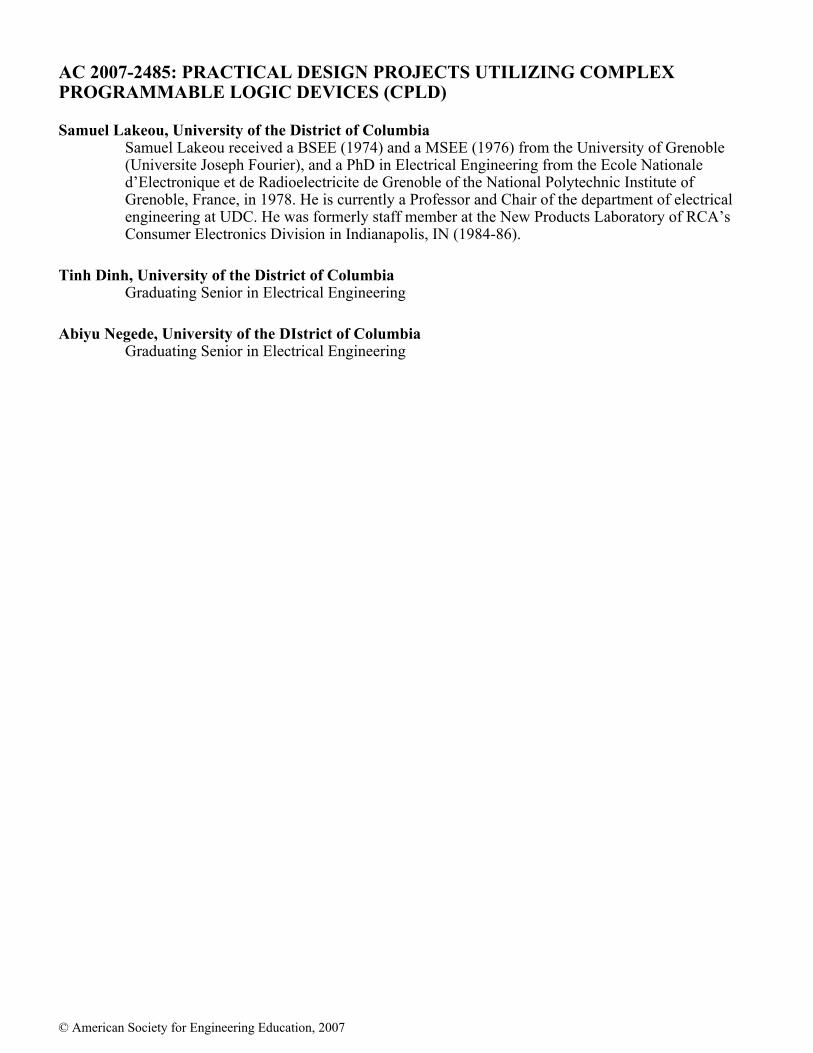
There are a variety of evaluation boards3 available on the market for PLD and FPGA’s in particular. However, a typical CPLD based requires no more than the design tools such as the ISE1 of Xilinx, a programming cable, a CPLD chip and a plastic leaded chip carrier (PLCC) packaged chip holder. Fig. 3 illustrates the basic components of a CPLD-based design system.
. a) PC with Integrated Synthesis Environment (ISE)
b) Programming Cable c) PLCC Adapter Socket d) Prototype Board
Fig. 3 Basic CPLD-Based design tools
III. Design Examples
A. Design of a Programmable Controller of an Ultrasonic Sonar Transducer and a
RC Servo:
In this design, an ultrasonic sonar transducer (UST) is placed on a radio controlled (RC) servo for target detection in a 180o angle sweep. The presence of a target triggers an alarm signal. The block diagram of the design is shown in Fig. 4.
The RC servo’s clockwise and anticlockwise movements are controlled by generating a 5-V, pulse width modulated (PWM) signal. A periodic signal with pulse widths of 1ms, 1.5ms and 2ms to provide a 180o sweep for target detection. A voltage proportional to the distance between target and the UST is continuously converted by an analog to digital (ADC) and fed to the CPLD. The CPLD selected for this project Xilinx’x XC9572XL4 . When a critical distance indicating the imminent presence of a target is sensed, the CPLD will decide to sound an alarm. The CPLD must also provide all the necessary control signals for operating the selected ADC, ADC0809 shown in Fig 5 and its associated timing diagram of Fig 6.
Fig. 4 Block diagram of a an UST controller circuit
IN0IN1IN2IN3IN4IN5IN6IN7STARTALEABC
CLOCKY0Y1Y2Y3Y4Y5Y6Y7
EOCOE
ADC 0809
Signal recieved from UST
Start pin connected from CPLD
500 kHz
8 bits outputs connected to CPLD
Fig. 5 ADC required control (note that the INVERTER and AND gates are “programmed”
in the CPLD
ADC0809
500kHz
ALARM
CPLD
XC 9572
RC Servo &
UST
Target
CLOCK
Fig. 6 Timing diagram of the ADC0809
The design entry of the design was done with VHDL. The VHDL code generates 3 different pulse widths (PW) to a 50 Hz, 5V pulse. A 5 MHz clock is used for generating through programmed frequency dividers, the various PWM signals as well as the clock, the start signal and address latch enable (ALE) signal for the ADC. A portion of the VHDL code written through ISE is shown in Fig. 7.
Fig. 7 VHDL (excerpt) code describing the UST controller circuit
When the voltage generated by the UST generates an analog voltage at 2.5 V an alarm signal will be generated. If the target object is not removed, the alarm will sound again in 2 second and off again. The sweep is stopped until the object is removed. The top level block representation of the design is displayed in Fig. 8. The block shows 8 inputs received from ADC0809, the main clock source, Clk (5 Mhz), the end of conversion signal (EOC) of the ADC, the ‘stop’ signal used to freeze the position of the servo, the clock signal of the ADC, ADCLK (500 kHz), an alarm output signal, Buzz, the output enable (OE) and start (START) of the ADC, and the control signal of the RC servo.
Fig. 8 Final block of UST and RC Servo controller
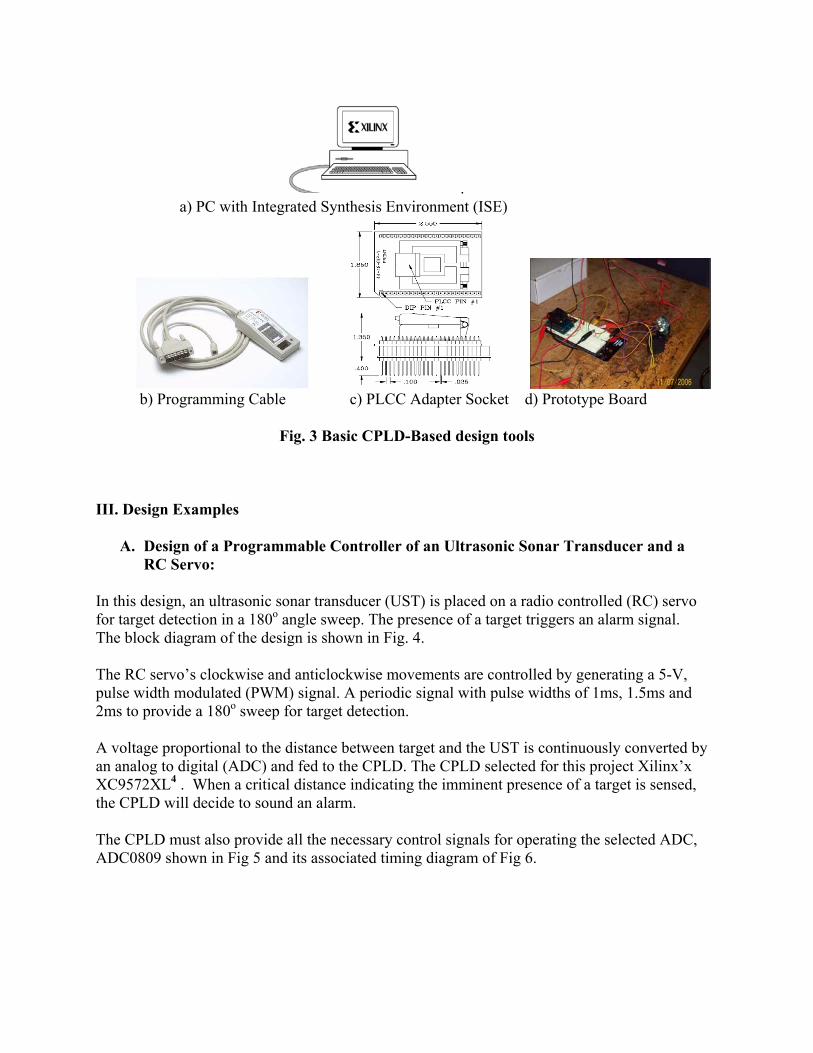
The prototype of the finished project is shown in Fig. 9.
Fig. 9 Prototype board built with CPLD XC9572
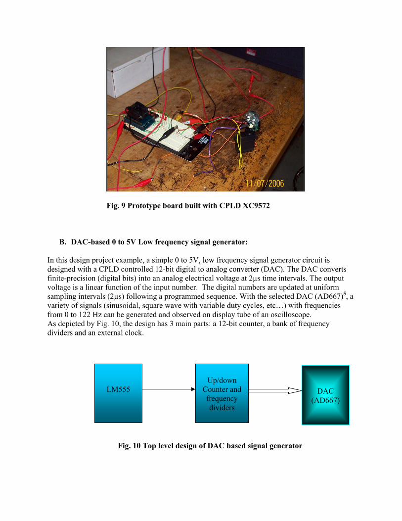
B. DAC-based 0 to 5V Low frequency signal generator:
In this design project example, a simple 0 to 5V, low frequency signal generator circuit is designed with a CPLD controlled 12-bit digital to analog converter (DAC). The DAC converts finite-precision (digital bits) into an analog electrical voltage at 2µs time intervals. The output voltage is a linear function of the input number. The digital numbers are updated at uniform sampling intervals (2µs) following a programmed sequence. With the selected DAC (AD667)5, a variety of signals (sinusoidal, square wave with variable duty cycles, etc…) with frequencies from 0 to 122 Hz can be generated and observed on display tube of an oscilloscope. As depicted by Fig. 10, the design has 3 main parts: a 12-bit counter, a bank of frequency dividers and an external clock.
DAC (AD667)
Up/down
Counter and frequency
dividers
LM555
Fig. 10 Top level design of DAC based signal generator
The maximum frequency of the clock corresponding to the sampling frequency of the DAC should be 500 kHz. An external timer, a 555 timer was designed for generating the clock. Fig. 11 shows the basic circuit of the timer.
762
3
4 851
LM555
0.01 uF
C
Rb
Ra
+5V
Output
Fig. 11 Clock generator circuit
The values of Ra and Rb and C are calculated with the standard formulas:
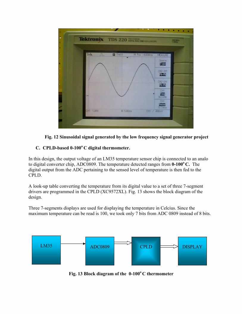
Yielding the values: Ra = 820 kµ, Rb = 1 Mµ, C = 1 pF The 12 bit up/down counter counts from 0 to 4095 then back from 4094 until it reaches 0 again. This procedure will repeat automatically as long as the clock is applied to this counter. The counter block of the design provides a conversion activation signal to the AD667. A settling time of about 70ns is required before the start of each conversion. The frequency divider portion of the design provides a range of frequencies which can be selected with an 8 -1 multiplexer. The design followed the typical design flow outlined earlier. The Design entry was performed with a description of the circuit with VHDL. Fig. 16 shows a 30Hz sinusoidal signal generated by the circuit.
Fig. 12 Sinusoidal signal generated by the low frequency signal generator project
C. CPLD-based 0-100o C digital thermometer.
In this design, the output voltage of an LM35 temperature sensor chip is connected to an analo to digital converter chip, ADC0809. The temperature detected ranges from 0-100
o C. The
digital output from the ADC pertaining to the sensed level of temperature is then fed to the CPLD. A look-up table converting the temperature from its digital value to a set of three 7-segment drivers are programmed in the CPLD (XC9572XL). Fig. 13 shows the block diagram of the design. Three 7-segments displays are used for displaying the temperature in Celcius. Since the maximum temperature can be read is 100, we took only 7 bits from ADC 0809 instead of 8 bits.
ADC0809
CPLD DISPLAY
LM35
Fig. 13 Block diagram of the 0-100o C thermometer
The simulation of the three 7-segment driver signals is shown in Fig. 14. The signals a[6:0] represent the 7-bit outputs carrying the digital values of the temperature. D1[6:0], D2[6:0] and D3[6:0] represent the driver signals.
Fig. 14 Simulation of the 7-segment driver signals of the thermometer
The top level circuit block of the thermometer is shown in Fig. 15.
Fig. 15 Top level thermometer block
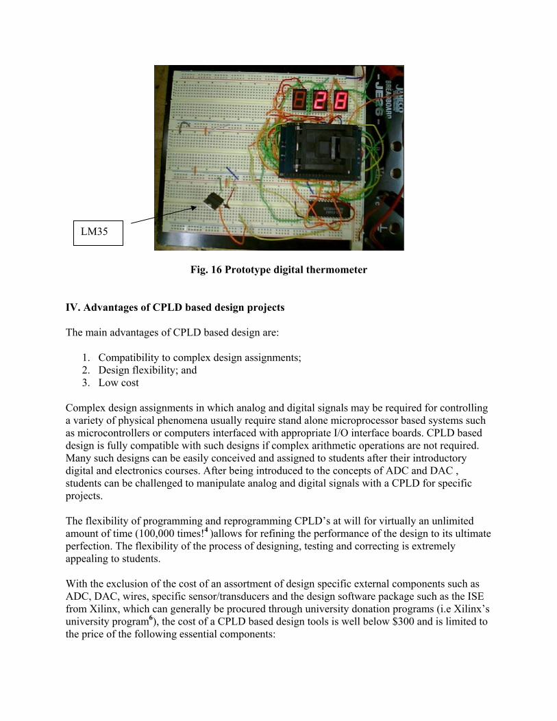
A circuit prototype board, as shown in Fig. 16. was built and was successfully tested.
LM35
Fig. 16 Prototype digital thermometer
IV. Advantages of CPLD based design projects
The main advantages of CPLD based design are:
1. Compatibility to complex design assignments; 2. Design flexibility; and 3. Low cost
Complex design assignments in which analog and digital signals may be required for controlling a variety of physical phenomena usually require stand alone microprocessor based systems such as microcontrollers or computers interfaced with appropriate I/O interface boards. CPLD based design is fully compatible with such designs if complex arithmetic operations are not required. Many such designs can be easily conceived and assigned to students after their introductory digital and electronics courses. After being introduced to the concepts of ADC and DAC , students can be challenged to manipulate analog and digital signals with a CPLD for specific projects. The flexibility of programming and reprogramming CPLD’s at will for virtually an unlimited amount of time (100,000 times!4 )allows for refining the performance of the design to its ultimate perfection. The flexibility of the process of designing, testing and correcting is extremely appealing to students. With the exclusion of the cost of an assortment of design specific external components such as ADC, DAC, wires, specific sensor/transducers and the design software package such as the ISE from Xilinx, which can generally be procured through university donation programs (i.e Xilinx’s university program6), the cost of a CPLD based design tools is well below $300 and is limited to the price of the following essential components:
a) Programming cable such as the parallel cable III or IV from Xilinx (~ $135) b) CPLD chip ($5-10); and c) PLCC packaged chip holder ($ 181 for 44 pin holder)
V. Conclusion
CPLD based design was introduced in the programs of electrical engineering and computer engineering at the University of the District of Columbia for the past few semesters. More recently, in the fall 06 semester, the first of a sequence of two senior project courses was dedicated to three mini-projects assigned all involving CPLD-based design. The outcome of the projects was very encouraging. Students who have completed the sequence of two required courses in digital design and two electronics courses were very pleased to see that they can handle a complex design assignment in a relatively short time. The ease with which they construct a working prototype of their design gives them added impetus to their design experience. References:
1. ISE 8.2i Software Manuals and Help (http://www.xilinx.com/support/sw_manuals/xilinx82/) 2. Modelsim SE (http://www.mentor.com/products/fv/digital_verification/modelsim_se/index.cfm) 3. Xilinx development boards (http://www.xilinx.com/products/devboards/) 4. XC9572XL in-system programmable CPLD data sheet
(http://direct.xilinx.com/bvdocs/publications/ds065.pdf) 5. AD667, Microprocessor-compatible 12-bit DAC (http://www.analog.com/en/prod/0,2877,AD667,00.html) 6. Xilinx University Program (http://www.xilinx.com/univ/)