Accelerated life-test methods and results for implantable electronic devices with adhesive encapsulation Xuechen Huang 1,2 & Petcharat May Denprasert 2 & Li Zhou 1 & Adriana Nicholson Vest 1 & Sam Kohan 2 & Gerald E. Loeb 1,2 Published online: 24 May 2017 # Springer Science+Business Media New York 2017 Abstract We have developed and applied new methods to estimate the functional life of miniature, implantable, wireless electronic devices that rely on non-hermetic, adhesive encapsulants such as epoxy. A comb pattern board with a high density of interdigitated electrodes (IDE) could be used to detect incipient failure from water vapor condensation. Inductive coupling of an RF magnetic field was used to pro- vide DC bias and to detect deterioration of an encapsulated comb pattern. Diodes in the implant converted part of the received energy into DC bias on the comb pattern. The capac- itance of the comb pattern forms a resonant circuit with the inductor by which the implant receives power. Any moisture affects both the resonant frequency and the Q-factor of the resonance of the circuitry, which was detected wirelessly by its effects on the coupling between two orthogonal RF coils placed around the device. Various defects were introduced into the comb pattern devices to demonstrate sensitivity to failures and to correlate these signals with visual inspection of failures. Optimized encapsulation procedures were validat- ed in accelerated life tests of both comb patterns and a func- tional neuromuscular stimulator under development. Strong adhesive bonding between epoxy and electronic circuitry proved to be necessary and sufficient to predict 1 year pack- aging reliability of 99.97% for the neuromuscular stimulator. Keywords Accelerated life test . Non-hermetic packaging . Encapsulation . Wireless . Implantable 1 Introduction A long functional lifetime is critical for clinical applications of most implantable medical devices. This is usually evalu- ated by accelerated life-testing in which failure modes that might occur after years of normal use are revealed more quickly by increasing the temperature and duty cycle. One common source of failures is the device packaging that is designed to protect the electronic components from body fluids and protects the body from the electronic components (Stieglitz 2010). Hermetic packages employing exotic met- al and ceramic technologies have few long-term failure modes but tend to result in relatively expensive, bulky and rigid devices that must be implanted surgically. For appli- cations requiring treatment for months to years rather than decades, such packaging is unnecessary. Polymeric encap- sulation was used with considerable success in the early days of pacemakers and spinal cord stimulators. Non- hermetic encapsulated devices can be inexpensive and reli- able, permitting small and elongated shapes that can be im- planted via minimally invasive procedures (Kim et al. 2009, Stieglitz 2010). However, this type of encapsulation may still fail within months to years due to diffusion and con- densation of water vapor and corrosion of electronic com- ponents (Hassler et al. 2011, Wang et al. 2013). Its integrity depends on conformal layer adhesion to component sur- faces rather than a diffusion barrier (Vanhoestenberghe and Donaldson 2013). Such adhesion can fail over time as a result of various stressors, so it is important to test such devices under actual use conditions, but it may be imprac- tical to do so for the design life of the device. The alternative is to introduce higher than usual aging factors (such as tem- perature, voltage, pressure, usage level, etc., or combina- tions thereof) to cause test units to fail more rapidly than under usual conditions (Nelson 1980, Escobar and Meeker * Xuechen Huang [email protected]1 Department of Biomedical Engineering, University of Southern California, Los Angeles, CA, USA 2 General Stim Inc., Los Angeles, CA, USA Biomed Microdevices (2017) 19: 46 DOI 10.1007/s10544-017-0189-9
Transcript
Accelerated life-test methods and results for implantableelectronic devices with adhesive encapsulation
Xuechen Huang1,2 & Petcharat May Denprasert2 & Li Zhou1& Adriana Nicholson Vest1 &
Sam Kohan2& Gerald E. Loeb1,2
Published online: 24 May 2017# Springer Science+Business Media New York 2017
Abstract We have developed and applied new methods toestimate the functional life of miniature, implantable, wirelesselectronic devices that rely on non-hermetic, adhesiveencapsulants such as epoxy. A comb pattern board with a highdensity of interdigitated electrodes (IDE) could be used todetect incipient failure from water vapor condensation.Inductive coupling of an RF magnetic field was used to pro-vide DC bias and to detect deterioration of an encapsulatedcomb pattern. Diodes in the implant converted part of thereceived energy into DC bias on the comb pattern. The capac-itance of the comb pattern forms a resonant circuit with theinductor by which the implant receives power. Any moistureaffects both the resonant frequency and the Q-factor of theresonance of the circuitry, which was detected wirelessly byits effects on the coupling between two orthogonal RF coilsplaced around the device. Various defects were introducedinto the comb pattern devices to demonstrate sensitivity tofailures and to correlate these signals with visual inspectionof failures. Optimized encapsulation procedures were validat-ed in accelerated life tests of both comb patterns and a func-tional neuromuscular stimulator under development. Strongadhesive bonding between epoxy and electronic circuitryproved to be necessary and sufficient to predict 1 year pack-aging reliability of 99.97% for the neuromuscular stimulator.
Keywords Accelerated life test . Non-hermetic packaging .
Encapsulation .Wireless . Implantable
1 Introduction
A long functional lifetime is critical for clinical applicationsof most implantable medical devices. This is usually evalu-ated by accelerated life-testing in which failure modes thatmight occur after years of normal use are revealed morequickly by increasing the temperature and duty cycle. Onecommon source of failures is the device packaging that isdesigned to protect the electronic components from bodyfluids and protects the body from the electronic components(Stieglitz 2010). Hermetic packages employing exotic met-al and ceramic technologies have few long-term failuremodes but tend to result in relatively expensive, bulky andrigid devices that must be implanted surgically. For appli-cations requiring treatment for months to years rather thandecades, such packaging is unnecessary. Polymeric encap-sulation was used with considerable success in the earlydays of pacemakers and spinal cord stimulators. Non-hermetic encapsulated devices can be inexpensive and reli-able, permitting small and elongated shapes that can be im-planted via minimally invasive procedures (Kim et al. 2009,Stieglitz 2010). However, this type of encapsulation maystill fail within months to years due to diffusion and con-densation of water vapor and corrosion of electronic com-ponents (Hassler et al. 2011, Wang et al. 2013). Its integritydepends on conformal layer adhesion to component sur-faces rather than a diffusion barrier (Vanhoestenbergheand Donaldson 2013). Such adhesion can fail over time asa result of various stressors, so it is important to test suchdevices under actual use conditions, but it may be imprac-tical to do so for the design life of the device. The alternativeis to introduce higher than usual aging factors (such as tem-perature, voltage, pressure, usage level, etc., or combina-tions thereof) to cause test units to fail more rapidly thanunder usual conditions (Nelson 1980, Escobar and Meeker
2006). It is also important, however, to avoid introducingfailure modes that may be specific to the test methods, suchas adding connections to energizing and monitoringinstrumentation.
The most commonly used acceleration factor is elevatedtemperature, but many components including the polymericencapsulant may have limited operating temperature ranges,such as its glass transition temperature. An alternative is todetect incipient failure at an early stage by using a highlysensitive test device. Rather than waiting for water to con-dense, corrode and cause circuit failure, a more sensitiveBcomb pattern^ consisting of many closely interdigitated ele-ments is used detect initial water molecule diffusion and con-densation. Traditionally, the encapsulated comb pattern deviceis made with two wire connections to an external powersource for DC bias voltage and to an impedance spectrometerto monitor package performance (Bierwagen et al. 2003). ADC bias applied across the comb pattern results in a uniformlyhigh voltage stress (V/cm) over a large test area. Moisturebetween the electrodes of the comb pattern greatly increasesthe capacitance and reduces the resistance between them. Thecombination of elevated temperature, elevated voltage stress,and high sensitivity to incipient failure provides an acceleratedvalidation of encapsulants.
Connecting external leads to the comb pattern may be diffi-cult or impossible without changing the structure and fabrica-tion procedure of the clinical device, which can lead to inaccu-rate extrapolation of lifetime and reliability (Yacobi et al. 2002).Furthermore, lead connection may not even be possible for thenext generation of devices that use bi-directional wireless trans-mission of power and data (Loeb et al. 2001, Zhou et al. 2016).Some implantable devices such as RF identification (RFID)Bbiochips^, video cameras, photonic stimulators and drug de-livery pumps may not normally have any externalized electricalconnections (Gensler et al. 2012, Koulaouzidis et al. 2015). Weutilized non-contact methods to detect changes in the resonanceof tuned inductor-capacitor circuits, which have long been usedin radio engineering, intracranial pressure monitors (Chubbuck1977) and other applications (Ong and Grimes 2000).
In this study, we have developed and tested wireless accel-erated life-testing methods to evaluate the epoxy packagingperformance of a wireless neuromuscular microstimulatorcalled NuStim™, which is designed to exercise the pelvicfloor muscle in stress urinary incontinence patients for up toone year (Huang et al. 2017). The ceramic circuit board in themicrostimulator was replaced by the comb pattern board toincrease sensitivity to incipient failure mechanisms. The de-vices were stressed by increased temperature, voltage and du-ty cycle in saline. We developed a non-contact method tomeasure the resonant frequency and quality factor of the ca-pacitive comb pattern connected to the same inductive coilthat normally receives power. Comb pattern devices with dif-ferent known defects were tracked over time to validate
sensitivity to failure mechanisms. Different cleaning and fab-rication procedures were compared during the study. Failurerates under these accelerated conditions were extrapolatedmathematically to estimate package reliability under normaluse conditions for the microstimulator.
2 Design and methods
2.1 Comb pattern
The comb pattern device (Fig. 1a) used the same constructionas the microstimulator (Fig. 1b) described elsewhere (Huanget al. 2017). The package consists of a thin-wall borosilicateglass sleeve that was filled with a low permeability epoxy(Epotek #302-3 M, Epoxy Technology Inc.). The comb pat-tern was printed on an aluminum oxide ceramic substrate(2.4 mm width × 3 mm length) by photolithography(deposited layers of gold over nickel, gold, and titanium-tungsten) with the spacing between the electrodes about25 μm, as shown in Fig. 2a. The surface mount discrete com-ponents were placed on the ceramic PCB board by hotplatesoldering at 230 °C (solder paste: WS488-SAC305, AIM sol-der, CA, USA). The external radio frequency power was re-ceived by a machined ferrite core with wound coil (26.5 turnsof 0.003″ insulated copper). The complete electronic assem-bly was cleaned thoroughly as described below and slippedinto a clean glass capillary. The epoxy was de-gassed in avacuum chamber, drawn into a syringe, and centrifuged tofurther remove bubbles. Then the epoxy was injected througha plastic tube slipped over the subassembly while applying avacuum to the other end. The epoxy was cured at 40 °C and230 psi to accelerate polymer crosslinking and prevent dis-solved air from forming bubbles. After overnight curing, theplastic tube and excess epoxy was cut away and the electrodesurfaces exposed cleanly by abrasive buffing.
The interdigitated electrodes of the comb pattern functionas a capacitor C that was connected in parallel with the wind-ing coil L to achieve inductive power transmission and encap-sulation failure detection (Fig. 2b). The capacitor C and theinductive coil L in parallel resonate at a frequency fSRF, deter-mined by:
f SRF ¼ 1
2πffiffiffiffiffiffiLC
p ð1Þ
The value of capacitance C depends on the dielectric prop-erties of the material between the electrodes. Any condensedmoisture present will substantially increase C because the di-electric constant of water (ɛ = 80.4) is much larger than epoxy(ɛ = 3.6). This will change the self-resonant frequency of thecircuit. Condensed moisture will also greatly reduce the resis-tance between the electrodes of the comb pattern by providing
46 Page 2 of 12 Biomed Microdevices (2017) 19: 46
a conductive liquid path between them. This can be detectedby a decrease in the quality factor (Q factor) of the circuitbased on the equation for a RLC parallel circuit,
Q ¼ R
ffiffiffiffiCL
r¼ f SRF
Δ fð2Þ
The Q factor can be computed by dividing the self-resonantfrequency fSRF by the bandwidthΔf, whereΔf is identified bya 3db decrease in the amplitude of a received RF signal.
The comb pattern device has the functionality to introduceDC bias voltage as an accelerating stressor. The comb patternboard is separated into two capacitors C1 and C2 in parallel asshown in the schematic (Fig. 2b). The introduced Zener diodes(GDZT2R8.2, RohmSemiconductor) do not affect the resonantfrequency of the circuit, which is mainly determined by theparallel C1 and C2. One side of the comb pattern C1 is con-nected to the inductive coil terminals directly to receive the ACsignal. The other half of the comb pattern C2 is connected inseries with the Zener diodes to introduce a DC voltage biasbetween the capacitor electrodes. A high voltage sinusoidalAC signal is generated across C1 and C2 branches equallyduring resonance. The Zener diodes provide half-wave rectifi-cation that is limited to the reverse-bias breakdown voltage ofthe Zener diodes (8VDC each, in-series total 16VDC). C2 in-tegrates the difference between high forward current throughthe Zeners when the positive phase of the received AC wave-form exceeds their forward bias and the low reverse current
during the negative phase until they reach their negativeZener threshold. This results in a bias voltage (measurementdescribed in Results) that provides the desired voltage stressacross the interleaved electrodes that form C2. Epoxy withdissolved and condensed water form virtual resistors R1 andR2 between the capacitor electrodes shown in the schematic.
A total of 12 comb pattern devices with three differentcommon defects during fabrication process were made todemonstrate sensitivity to failures. 1) Bubble defects wereinduced intentionally in the epoxy injection step withundegassed epoxy and injection without a vacuum. 2)Finger print oil was introduced after final cleaning by swipinga cotton swab contaminated with finger oil over the surface ofthe comb pattern before encapsulation. 3) Contamination by acyanoacrylate adhesive (normally used to mount the PCB andcontrol the terminations of the coil) was applied by hand.
Preliminary work had suggested that epoxy adhesion wasadversely affected by using deionized water instead of dis-tilled water in the final rinsing step of the PCB cleaning pro-cess before epoxy encapsulation. Two groups of 20 combpattern devices each were constructed to evaluate the differ-ences using the following cleaning procedures (Table 1) be-fore epoxy encapsulation (as described above): 1) The combpatterns designated BDeion. Clean^were flushed by isopropylalcohol (IPA) for 30s and brushed if there was visible debrisleft on the board., then rinsed with deionized water for 30s anddried in the oven for 2 h, and 2) The comb patterns designatedBDist. Clean^ were placed in separate clean vials for
Fig. 2 a Comb pattern ceramicPCB board with IDE. bSchematic of comb pattern board.C1 and C2 represent thecapacitors circled by red andblack dotted lines in the PCBboard. R1 and R2 representvirtual resistance in parallel withcapacitors. L1 is the winding coilon ferrite. Z1 and Z2 are Zenerdiodes
Fig. 1 Design of comb patterndevice compared to clinicalNuStim microstimulator. a Combpattern device before epoxyfilling. b Microstimulator afterencapsulation
Biomed Microdevices (2017) 19: 46 Page 3 of 12 46
ultrasound cleaning with IPA (10 min.) and distilled water(10 min.), then dried in the oven for 2 h.
2.2 Functional device
After the studies of comb pattern devices, 9 functionalmicrostimulators were fabricated and encapsulated accordingto the final cleaning procedure as shown in Table 1, whichincluded some further improvements. Before the coil windingprocedure, any loose particulates from the machined ferriteswere removed by sonicating in detergent for 10 min. (1%detergent in distilled water, Detergent 8, Alconox, NY,USA) and then rinsed with distilled water to flush out residualdetergent. The PCB was placed on the ferrite using the sameepoxy adhesive as for encapsulation instead of cyanoacrylate.The functional device was cleaned before the wire bonding bythe same cleaning procedure as for the final subassembly. Thefinal subassembly was rinsed after ultrasonic cleaning by dis-tilled water to flush out any contaminants from the ultrasonicbath.
2.3 Wireless detection
The bandwidth and resonant frequency of the LC circuit ofthe comb pattern devices were detected wirelessly by theconcentric, orthogonal, inductive coil pair shown in Fig. 3a.The coils were carefully aligned to minimize direct induc-tive coupling between the transmitter and receiving coils byfinding the null orientation at all test frequencies. The func-tion generator (Tektronix AFG3102 Dual Channel Functiongenerator) generated a sinusoidal sweep frequency 16–24 MHz at 10 Vp-p to provide power to the transmitter coil.The device under test was inserted at 45 degrees into thecenter of both coils. The output voltage of the receiver coilwas recorded on the oscilloscope to determine resonant fre-quency and bandwidth. When the frequency of the
transmitted magnetic field equals the resonant frequencyof the device under test, it induces a maximal circulatingcurrent in the LC circuit. The induced current flow in thecoil of the device under test creates its own magnetic field,which is picked up by the receiving coil of the test system.The self-resonant frequency (green trace in Fig. 3b) of a
Fig. 3 a Two coil wireless query system for resonant frequency andbandwidth detection. The powering coil (2 turns of 18 AWG insulatedcopper wire, 37.5 mm in diameter) and the detecting coil (30 turns 22AWG insulated copper wire, 35 mm in diameter) were placedorthogonally to minimize direct electromagnetic coupling betweenthem. The test article was placed at 45° angle between them so that itcoupled to both coils. bOscillogram of self-resonant frequency and band-width (green trace) as measured in wireless detection, sweeping from 16to 24 MHz. Generated bias DC voltage (yellow trace) on the diodes asmeasured by needle probes is correlated to device’s resonant properties
comb pattern device was measured by the receiving coil asdisplayed on oscilloscope, which was ~20.7 MHz with~1 MHz bandwidth before encapsulation. The bias DCvoltage (yellow trace in Fig. 3b) was also measured duringwireless detection and was found to be correlated with themeasured resonant properties of the device under test.Instead of directly probing the comb pattern capacitor,which is the summation of the both the capacitor outputand the bias, the bias DC voltage was measured directlyusing fine needle probes between Zener diodes. The biasDC voltage tended to drop substantially when the self-resonant frequency and/or Q factor of the device was affect-ed by moisture applied on the bare comb pattern board.
2.4 Wireless powering
The comb pattern devices were powered inductively duringaccelerated life-testing by a custom transmitter coil drivenby a class E power amplifier. The external power sourceproduced a 20 MHz continuous electromagnetic field atleast 10 A/m strength up to 10 cm distance from the planeof the coil. The design of this RF powering system andmethods to measure and optimize power output were sim-ilar to those described previously for the microstimulator(Vest et al. 2016). When the devices were around 20 MHz,Q factor at 15, and placed at various distances above the RFtransmitter, the measured Zener-regulated bias DC voltageas displayed on oscilloscope was stable at ~11.5 VDC fordistances up to 10 cm and tilt angles to 45° from vertical.The bias DC voltage is not regulated at the ideal voltage(16 V) due to component frequency characteristics. Duringthe accelerated life-testing, the resonant frequency and Qfactor would drop due to comb pattern capacitance andresistance changes, which decreased the DC bias voltage.The data points in Fig. 4 were acquired by adding differentvalues of capacitors or resistors in parallel with C2 and R2in the bare comb pattern board, respectively, to shift theresonant frequency or Q factor independently. Fig. 4a plotsvalue of the bias DC voltage as a function of self-resonantfrequency when the Q factor was maintained at 15.5 ± 0.4(mean ± standard deviation). The bias DC voltage depen-dency on Q factor is shown in Fig. 4b when the self-resonant frequency was maintained at 20.0 ± 0.4 MHz(mean ± standard deviation). By measuring the self-resonance frequency and calculating the Q factor, the biasDC voltage can be conservatively estimated using the fittedcurves. For example, if one device had self-resonant fre-quency at about 19 MHz, the bias voltage would be about7 V and 4.7 V when Q factor was about 15 and 10, respec-tively, based on the fitted curve. It is important to note thatshifts of this magnitude for resonant frequency and Q werealways associated with rapid further shifts that led to devicefailure as defined below.
2.5 Accelerated life-testing
After initial baseline measurement, all comb pattern de-vices were positioned vertically inside a saline tank at50 °C for accelerated life-testing (Fig. 5a) and were re-moved at regular intervals for wireless detection (Fig. 3a)of their resonant properties. A saline tank was placed overthe transmitter coil, and the devices were powered contin-uously via inductive coupling. Its temperature was moni-tored by an electromagnetically shielded thermocouple andregulated by a circulating water bath with accuracy of±1 °C.
If the measured resonant properties of comb pattern de-vices met the criteria for incipient failure (resonantfrequency ≤ 17 MHz), the devices were examined carefullyunder a microscope to identify possible failure mecha-nisms. As indicated by the fitted curve in Fig.4, when theresonant frequency was around 17 MHz with Q factorabout 7, the voltage stress on the comb pattern droppedbelow 0.5 V, which would be insufficient to drive mostelectrolysis reactions. From the preliminary experiments,whenever the self-resonant frequency was lower than17 MHz or there was no detectable resonant frequency,there were visible gross failures including ionic dissolution,galvanic corrosion and dendrite formation, bridging, andshort-circuits between comb pattern traces.
Data was collected for one year in accelerated life-test-ing. The time to failure of the device was derived from theresonant properties measurement that met failure criteria.An exponential distribution with constant failure rate wasassumed for the failure times of two groups of comb patterndevices (Deion. Clean and Dist. Clean groups) (Minnikantiet al. 2014). This was used to extrapolate the reliability ofepoxy encapsulation of the microstimulators for 1 year at37 °C, based on differences in the magnitude and distribu-tion of voltage stress levels between the two types of de-vice. One year of data collection in accelerated life-testingpredicts a much longer lifetime than the one year of inter-mittent use required for the intended clinical application ofthe neurostimulator.
The acceleration model used in the paper had three com-bined accelerating factors of temperature, voltage stressand duty cycle. Each individual accelerating factor wasassumed to be independent and to contribute to the accel-eration multiplicatively (Escobar and Meeker 2006). Theaccelerated life test was performed at 50 °C, below theglass transition temperature of the epoxy to avoid excessivethermal expansion and glass breakage. The aging factorwas determined by an empirical estimation of Arrhenius’Law, for which every 10 °C elevation results in twice ac-celeration of all chemical reactions (Hukins et al. 2008).The calculated acceleration factor was thus about 2.4 timesfaster in 50 °C compared to human body environment at
Biomed Microdevices (2017) 19: 46 Page 5 of 12 46
37 °C. The inverse power relation was used for non-thermalacceleration due to voltage stress:
AF ¼ Ea
Eu
� �β
where the acceleration factor AF is the ratio between theaccelerated voltage stress level and the normal voltagestress level. β =1 assumes that increased voltage stressmagnitude has positive, linear acceleration for the devicefailure. The effects of duty cycle were also estimated fromthe continuous stress in the accelerated life tester (24 h/d)divided by the maximal daily treatment prescription (2 h/d).
The functional microstimulators were powered in theaccelerated life-testing by a separate RF transmittertuned to the operating frequency of the microstimulatorat 6.78 MHz. Rather than placing the devices into salinetank directly as done with the comb pattern devices,each functional microstimulator was loaded into a testvial of saline equipped with Pt-Ir electrodes to captureits output pulses and a light emitting diode (LED) toprovide a visual monitor of its functionality (Fig. 5b).The vials were then placed into heated water bath at50 °C above the RF transmitter. The microstimulatorwas powered continuously with 20 ms long bursts ofRF every 33 ms, generating the maximal stimulus out-put through the LED of ~3 μC @ 30 pps with peakvoltage of 15 V. If and when the LED ceased blinking,
the device was removed from the test vial and examinedfor failure analysis.
3 Results
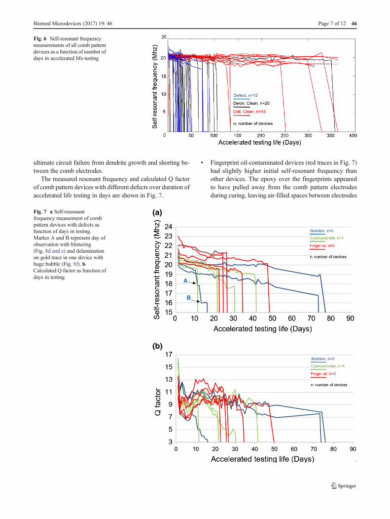
Measured self-resonant frequency of all comb pattern devicesas a function of accelerated life-testing in days is shown inFig. 6. Details regarding the failure rates for each type ofdeliberately introduced defect in the comb patterns are shownin Fig. 7. Each trace corresponds to the measurements overtime for one device, with color codes to indicate classificationaccording to details of fabrication that were intended to affectreliability. Generally, all devices experienced the same threephases but differed in the rate at which they progressed be-tween phases depending on fabrication classification. In phase1, self-resonant frequency around 20MHz dropped within thefirst couple days of soaking, representing water vapor diffu-sion into the epoxy encapsulant with dielectric change. Inphase 2, if there were no voids or unbounded cavities for watervapor condensation, the measurements were stable with onlyslight fluctuations that appeared to be related to environmentaltemperature changes. In phase 3, self-resonant frequency firstdropped below 17 MHz, with wide bandwidth and low Qfactor due to condensation of moisture, then progressed rap-idly towards undetectable resonant frequency, shown as asharp decline in the plot, representing metal corrosion and
Fig. 5 a Accelerated life testsystem for both comb patterndevices and the microstimulator.b Accelerated life-testing vial forthe microstimulator to convertstimulation pulses into visiblelight flashes. The rubber tube actsas an O-ring to force the outputstimulation current through thesurrounding saline and into the Pt/Ir wire electrodes, which do nottouch the output electrodes of themicrostimulator
Fig. 4 a Measured bias DCvoltage as self-resonant frequencychanges. b Measured bias DCvoltage as Q factor changes
46 Page 6 of 12 Biomed Microdevices (2017) 19: 46
ultimate circuit failure from dendrite growth and shorting be-tween the comb electrodes.
The measured resonant frequency and calculated Q factorof comb pattern devices with different defects over duration ofaccelerated life testing in days are shown in Fig. 7.
& Fingerprint oil-contaminated devices (red traces in Fig. 7)had slightly higher initial self-resonant frequency thanother devices. The epoxy over the fingerprints appearedto have pulled away from the comb pattern electrodesduring curing, leaving air-filled spaces between electrodes
`
A
B
(a)
(b)
Fig. 7 a Self-resosnantfrequency measurment of combpattern devices with defects asfunction of days in testing.Marker A and B represent day ofobservation with blistering(Fig. 8d and e) and delaminationon gold trace in one device withhuge bubble (Fig. 8f). bCalculated Q factor as function ofdays in testing
Fig. 6 Self-resonant frequencymeasurements of all comb patterndevices as a function of number ofdays in accelerated life-testing
Biomed Microdevices (2017) 19: 46 Page 7 of 12 46
that had lower dielectric constant than the epoxy.Compared with other devices, the finger print oil contam-inated devices usually failed most quickly due to directwater vapor condensation in the void and dendrite forma-tion between electrodes (Fig. 8a).
& Cyanoacrylate-contaminated devices (green traces inFig. 7) tended to initiate corrosion on the edge of thePCB where the low-viscosity adhesive could seep ontothe comb pattern before curing. This was associated withunreliable adhesion, corrosion, dendritic short circuits andundetectable self-resonant frequency (Fig. 8b). The dam-age could expand even after electrical function ceased(Fig. 8c).
& Bubble-defect devices (blue traces in Fig. 7) usually lastedlonger in accelerated life-testing than other devices, exceptfor one device with a huge bubble over the comb patternthat left only a thin layer of epoxy on the electrodes aftercuring. Water vapor condensation could be found in thebubble after 10 days of soaking (Fig. 8d). Optical micros-copy revealed blistering on the gold electrode (Fig. 8e)with progressive delamination (Fig. 8e) that was correlat-ed with resonant frequency measurements (markers A andB on Fig. 7a, respectively).
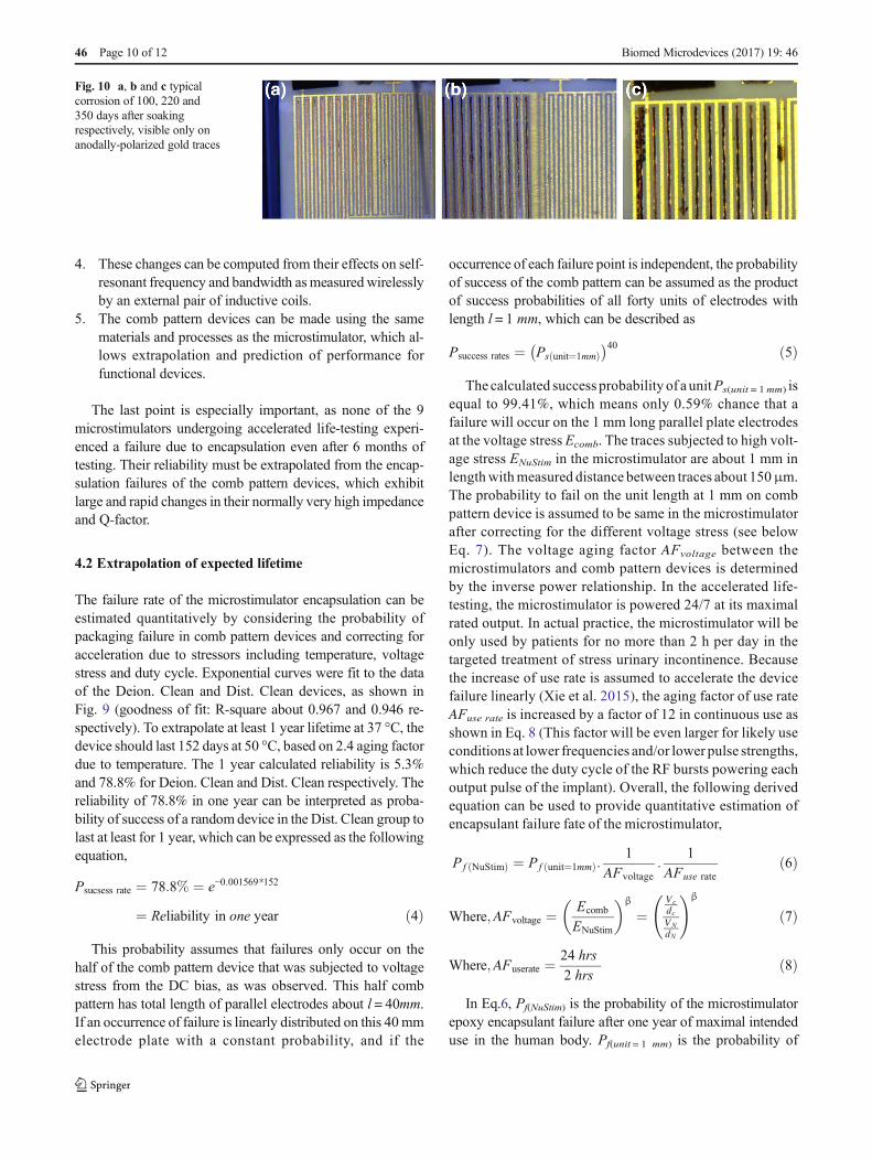
The percentages of surviving devices in the Deion.Clean and Dist. Clean groups are plotted over time inFig. 9. The Deion. Clean group had a total of 20 devicessubjected to the soaking test, whereas the Dist. Clean grouphad 13 devices after excluding 7 devices that failed fromunrelated manufacturing problems. In the Deion. Cleangroup, about 50% of devices failed after 30 days and 90%failed after 100 days. In the Dist. Clean group, about 54%(7 of the 13 devices) were still working after more than365 days in the accelerated life-testing. The survivingcomb pattern devices had stable self-resonant frequenciesaround 19 MHz with Q factor ~ 9, which was estimated togenerate 4.2 V voltage stress (see Fig. 5). Corrosion usuallystarted on the gold trace (Fig. 10a) and gradually increasedover time (Fig. 10b). Eventually, the epoxy barrier betweencomb pattern traces broke in at least one location, which ledto functional failure (Fig. 10c).
All 9 functional microstimulators were stressed contin-uously in the accelerated life-testing chamber. The survivalrate over time is shown in Fig. 9. Two devices failed after119 and 155 days; the other 7 devices were still functioningnormally after >180 days at 50 °C (equal to ~14 months at37 °C). The two failed devices were subjected to failureanalysis by applying various test signals to their outputelectrodes. Neither failure was related to epoxy encapsulantfailure. One device had no visible corrosion but had no self-resonant frequency; this is most likely caused by a coldsolder joint where the copper wire is attached to the ceramic
PCB. A procedure to pretin the copper wire before solder-ing to the PCB was added to alleviate this problem. Theother failed device had the characteristic appearance ofBpurple plague^ around one end of the gold bondwire toan aluminum pad on the programmable unijunction transis-tor in the stimulation circuit (Blish et al. 2007). This is aclassic example of interfacial intermetallic compound(IMC) formation when such bonds are poorly made andsubjected to high current flow.
4 Discussion
4.1 Interpretation of test data
The measured self-resonant frequency and calculated Qfactor of the comb pattern devices are both sensitive indi-cators of encapsulant performance. They are related toeach other, but Q factor provides additional information.In the first several days of testing, capacitance increasesas absorbed water vapor increases the dielectric constantof the epoxy encapsulant, which decreases self-resonantfrequency (Fig. 7a) and should increase Q factor (Fig. 7b).Instead, the Q factor decreases as the result of significantdecrease in resistance based on Eq. 2, which is related toan increase of epoxy conductivity from water vapor dis-solved in it (Bierwagen et al. 2003). As more water vapordiffuses through the epoxy, the Q factor then increases,which represents an increase of capacitance due to theexpected dielectric change from water vapor with no fur-ther change in resistance between traces. When water va-por reaches saturation, the measured Q factor becomesstable, indicating stable capacitance and resistance. Ifthe adhesive bonding is damaged, the resistance betweenelectrodes drops significantly, as indicated by a rapid de-crease of Q factor. The comb pattern circuity is not anideal RLC parallel circuit as shown in Eq. 2. The circuithas additional resistance introduced by the winding coilwire and impedance from the Zener diodes, which com-plicates the equivalent circuit. Rather than providingquantitative measurements, the circuit allows qualitativeevaluation of resistance and capacitance changes fromwater vapor diffusion and condensation.
One objective of this study is to determine and optimizethe long-term reliability of the epoxy encapsulation for awireless microstimulator. Instead of relying on long-termfunctional testing of complete devices, a comb pattern ispreferable for accelerated identification of failure modes inseveral ways:
1. It has a large area of high density of closely spaced con-ductors that are vulnerable to water condensation.
46 Page 8 of 12 Biomed Microdevices (2017) 19: 46
2. High voltage stress can be applied to accelerate incidenceof failure without introducing electrical connections thatmight change failure susceptibility.
3. Water vapor diffusion, condensation and corrosion aredetected as changes of capacitance and resistance to pro-vide an early indication of incipient device failure.
Fig. 9 Number of survived devices in deionized clean group (Deion.clean), distilled clean group (Dist. Clean) and neurostimulator group asa function of accelerated testing days (normalized to number of devices
starting soaking). The x-axis in green represents expected life in monthsat 37 °C, assuming only Arrhenius temperature acceleration
corrosioncorrosioncorrosion
BAA
(a)
(d) (e) (f)
(b) (c)Fig. 8 a Typical corrosion onIDE with finger print oilcontamination. b Typicalcorrosion on IDE with adhesivecontamination. c Increasedcorrosion area over time. d and eThe giant bubble filled with waterand blisters forming on the goldtraces. Markers A: opticalmicroscopy correlated withmeasured resonant frequency inFig. 7a. f Further delaminationformed along the gold trace.Marker B: optical microscopywas correlated with measuredresonant frequency in Fig. 7a
Biomed Microdevices (2017) 19: 46 Page 9 of 12 46
4. These changes can be computed from their effects on self-resonant frequency and bandwidth asmeasured wirelesslyby an external pair of inductive coils.
5. The comb pattern devices can be made using the samematerials and processes as the microstimulator, which al-lows extrapolation and prediction of performance forfunctional devices.
The last point is especially important, as none of the 9microstimulators undergoing accelerated life-testing experi-enced a failure due to encapsulation even after 6 months oftesting. Their reliability must be extrapolated from the encap-sulation failures of the comb pattern devices, which exhibitlarge and rapid changes in their normally very high impedanceand Q-factor.
4.2 Extrapolation of expected lifetime
The failure rate of the microstimulator encapsulation can beestimated quantitatively by considering the probability ofpackaging failure in comb pattern devices and correcting foracceleration due to stressors including temperature, voltagestress and duty cycle. Exponential curves were fit to the dataof the Deion. Clean and Dist. Clean devices, as shown inFig. 9 (goodness of fit: R-square about 0.967 and 0.946 re-spectively). To extrapolate at least 1 year lifetime at 37 °C, thedevice should last 152 days at 50 °C, based on 2.4 aging factordue to temperature. The 1 year calculated reliability is 5.3%and 78.8% for Deion. Clean and Dist. Clean respectively. Thereliability of 78.8% in one year can be interpreted as proba-bility of success of a random device in the Dist. Clean group tolast at least for 1 year, which can be expressed as the followingequation,
Psucsess rate ¼ 78:8% ¼ e−0:001569*152
¼ Reliability in one year ð4Þ
This probability assumes that failures only occur on thehalf of the comb pattern device that was subjected to voltagestress from the DC bias, as was observed. This half combpattern has total length of parallel electrodes about l = 40mm.If an occurrence of failure is linearly distributed on this 40mmelectrode plate with a constant probability, and if the
occurrence of each failure point is independent, the probabilityof success of the comb pattern can be assumed as the productof success probabilities of all forty units of electrodes withlength l = 1 mm, which can be described as
Psuccess rates ¼ Ps unit¼1mmð Þ� �40 ð5Þ
The calculated success probability of a unitPs(unit = 1mm) isequal to 99.41%, which means only 0.59% chance that afailure will occur on the 1 mm long parallel plate electrodesat the voltage stress Ecomb. The traces subjected to high volt-age stress ENuStim in the microstimulator are about 1 mm inlengthwithmeasured distance between traces about 150μm.The probability to fail on the unit length at 1 mm on combpattern device is assumed to be same in the microstimulatorafter correcting for the different voltage stress (see belowEq. 7). The voltage aging factor AFvoltage between themicrostimulators and comb pattern devices is determinedby the inverse power relationship. In the accelerated life-testing, the microstimulator is powered 24/7 at its maximalrated output. In actual practice, the microstimulator will beonly used by patients for no more than 2 h per day in thetargeted treatment of stress urinary incontinence. Becausethe increase of use rate is assumed to accelerate the devicefailure linearly (Xie et al. 2015), the aging factor of use rateAFuse rate is increased by a factor of 12 in continuous use asshown in Eq. 8 (This factor will be even larger for likely useconditions at lower frequencies and/or lower pulse strengths,which reduce the duty cycle of the RF bursts powering eachoutput pulse of the implant). Overall, the following derivedequation can be used to provide quantitative estimation ofencapsulant failure fate of the microstimulator,
Pf NuStimð Þ ¼ Pf unit¼1mmð Þ:1
AFvoltage:
1
AFuse rateð6Þ
Where;AFvoltage ¼ Ecomb
ENuStim
� �β
¼VcdcVNdN
!β
ð7Þ
Where;AFuserate ¼ 24 hrs2 hrs
ð8Þ
In Eq.6, Pf(NuStim) is the probability of the microstimulatorepoxy encapsulant failure after one year of maximal intendeduse in the human body. Pf(unit = 1 mm) is the probability of
Fig. 10 a, b and c typicalcorrosion of 100, 220 and350 days after soakingrespectively, visible only onanodally-polarized gold traces
46 Page 10 of 12 Biomed Microdevices (2017) 19: 46
failure of the comb pattern, which is 0.59%. The aging factorof voltage AFvoltage is 1.64, where voltage stress Ecomb =168 V/mm with Vc = 4.2 V and dc = 25 μm, and voltage stressENuStim = 100 V/mm with Vc = 15 V and dc = 150 μm, withassumption ofβ = 1 indicating a linear effect of voltage stress.
The quantitative estimation of the microstimulator failurerate at one year Pf(NuStim) is about 0.03% based on considerationof aging factors from temperature, voltage stress and use rate.This estimated rate is surprisingly low but further supported bythe observed result in the microstimulator accelerated life-test-ing, which had no devices failed due to encapsulation after180 days testing at elevated temperature and maximal output.All devices (excluding the two that failed for other reasons)have functioned for the equivalent of >1 year at 37 °C (theoriginal design goal for the clinical application) despite contin-uous powering. This conclusion must be tempered by the rela-tively small number of devices tested to date, which results in arelatively large statistical uncertainty about actual reliability.The accelerated life-test methods described herein now needto be applied systematically to larger samples of devices.According to parametric binomial statistics, 36 comb patterndevice samples with 4 failures occurring over 152 days in ac-celerated life-testing would demonstrate the claimed reliabilityat a 90% confidence level (Guo et al. 2013). The much higherreliability extrapolated for the microstimulators would require amuch larger sample and/or a much longer test period to confirmempirically. Conversely, failures occurring more frequentlywould suggest failure modes different from those related tothe epoxy encapsulation in the comb pattern devices.
Non-hermetic encapsulation relies on adhesive bonding tothe component surfaces that is maintained by electrostatic at-traction and mechanical interlocking (Yacobi et al. 2002). Thecleaning procedure is a critical step for encapsulation perfor-mance because even a monolayer of a surface contaminantcan prevent the necessary bonds from forming. The majorcontaminant residue left on a populated circuit board is fluxin the solder paste. It is formulated from many ionic and or-ganic compounds that include reactive species. The solderingproblem can be managed by using water soluble solder paste.The deionized water was not as effective as distilled water toclean the subassembly. Deionization removes ions such assodium and chloride but may leave or even introduce non-ionic contaminants. Deionized water is typically shipped andstored in plastic bottles, from which oligomers, catalysts, andplasticizers may leech. Water distilled and stored in glass bot-tles should be used for final rinses to prevent contaminantsfrom coating surfaces after the water evaporates away. Thefully cured epoxy Epotek 302-3M has high chemical stability,strong dielectric properties, low water uptake and slow diffu-sion rate; it was found to be a reliable encapsulant (Birkelundet al. 2011). Low permeability itself cannot prevent watervapor diffusion throughout a device as small as themicrostimulator, but it tends to be associated with low water
absorption; such absorption and swelling can produce me-chanical stresses that may disrupt chemical adhesion, leavingvoids for water condensation. Strong adhesion betweenencapsulant and active circuitry can reliably prevent watervapor condensation and corrosion for many years(Donaldson 1991). Although the epoxy thermal expansionwould induce extra pressure, thereby improving adhesionand decreasing the likelihood of delamination, it is negligiblein this study due to the small cross-sectional area of the epoxyabove the PCB and the low thermal expansion coefficient.
Although the comb pattern device has been made to mimicthe fabrication process of the functional wirelessmicrostimulator, there are still several differences that mayaffect the encapsulation performance in various ways. First,the microstimulator has more discrete components and com-plicated structure than the comb pattern device, which hasonly two Zener diodes on the PCB located away from thesensitive interdigitated electrodes. Compared to the unbrokenflat surface of the comb pattern, the microstimulator might besubjected to residual stress due to non-uniform shrinkage andshear forces from epoxy curing, which could introduce poten-tial voids for water vapor condensation. Although hybrid dis-crete electronic components are generally not vulnerable towater vapor, these components and their solder joints are sus-ceptible to liquid water that might condense in a void betweencomponents and circuit board or a cavity within a component.The cleaning procedure is sufficient to get rid of contamina-tion on the board when components are placed and solderedproperly. The controlled low rate of epoxy infiltration andcuring under pressure can help epoxy penetration into cavitiesand compress any residual bubbles to provide a defect-freeencapsulation (Loos and Springer 1983). Second, wire-bonding in microelectronic circuits is another vulnerabilitywith its own failure modes, which were not present in thecomb pattern devices. The thermosonic gold wire-bondingto aluminum pads in the microstimulator inevitably formsintermetallic compounds at the junction that tend to have poorelectrical conductivity, the source of the purple-plague failureof one device. Wire-bond quality is controlled by propercleaning procedure before bonding and the settings of thewire-bonding machine. Our cleaning procedure used ultra-sound with solvents to clean the pad surface, resulting in me-chanically acceptable wire-bonds with a breaking force of 7 to12 g. The thickness and resistance of the intermetallic com-pound at the gold-aluminum junction needs to be minimizedby providing an appropriate substrate temperature duringbonding (Breach and Wulff 2004, Xu et al. 2010).
5 Conclusion
We have evaluated the functional long-term reliability of min-iature, implantable, wireless electronic devices that rely on
Biomed Microdevices (2017) 19: 46 Page 11 of 12 46
non-hermetic, epoxy encapsulants. The lifetime was measuredby an encapsulated comb pattern with high density of inter-digitated electrodes that was used to detect incipient failures.The capacitance of the comb pattern forms a resonant circuitwith the inductor by which the implant receives power. Anymoisture affects both the resonant frequency and the Q-factorof the resonance, which was detected wirelessly by its effectson the coupling between two orthogonal RF coils placedaround the device. Inductive coupling of an RF magnetic fieldwas used in the accelerated life-testing to provide DC bias.Strong adhesive bonding between epoxy and electronic circu-ity proved to be necessary for package reliability; this can beachieved by proper cleaning and encapsulation procedures.Comb pattern devices were estimated to have 78.8% reliabil-ity for one year, which extrapolated to 1 year reliability of99.97% for the neuromuscular stimulator after accountingfor various stressors in the accelerated life-test. This is consis-tent with the results from accelerated life-testing of a smallsample of the microstimulators, in which there were noencapsulant failures even beyond 6 months of continuous out-put at elevated temperature.
Acknowledgements The authors would like to thank engineers RayPeck, Sisi Shi, and Longpeng Jiao for help in design and manufacturing.The project is funded by General Stim Inc.
References
G.Bierwagen, D. Tallman, J. Li, L. He, C. Jeffcoate, EIS studies of coatedmetals in accelerated exposure. Prog Org Coat 46(2), 149–158(2003)
K. Birkelund, L. Nørgaard, E.V. Thomsen, Enhanced polymeric encap-sulation for MEMS based multi sensors for fisheries research.Sensors Actuators A Phys. 170(1), 196–201 (2011)
R.C. Blish, S. Li, H. Kinoshita, S. Morgan, A.F. Myers, Gold–aluminumintermetallic formation kinetics. IEEE Trans. Device Mater. Reliab.7(1), 51–63 (2007)
C. Breach, F. Wulff, New observations on intermetallic compound for-mation in gold ball bonds: General growth patterns and identifica-tion of two forms of au 4 al. Microelectron. Reliab. 44(6), 973–981(2004)
J. G. Chubbuck, Intracranial pressure monitor, Google Patents (1977)P. Donaldson, Aspects of silicone rubber as an encapsulant for neurolog-
ical prostheses. Med. Biol. Eng. Comput. 29(1), 34–39 (1991)Escobar, L. A. and W. Q. Meeker. "A review of accelerated test models."
Statistical science: 552–577 (2006)H. Gensler, R. Sheybani, P.-Y. Li, R.L. Mann, E. Meng, An implantable
MEMS micropump system for drug delivery in small animals.Biomed. Microdevices 14(3), 483–496 (2012)
H. Guo, E. Pohl, A. Gerokostopoulos, Determining the right sample sizefor your test: theory and application. 2013 Annual Reliability andMaintainability Symposium, Available from http://www.reliasoft.com/pubs/2013_RAMS_determining_right_sample_size.pdf.Accessed on 5 June 2014 (2013)
C. Hassler, T. Boretius, T. Stieglitz, Polymers for neural implants. J.Polym. Sci. B Polym. Phys. 49(1), 18–33 (2011)
D. Hukins, A. Mahomed, S. Kukureka, Accelerated aging for testingpolymeric biomaterials and medical devices. Med. Eng. Phys.30(10), 1270–1274 (2008)
S. Kim, R. Bhandari, M. Klein, S. Negi, L. Rieth, P. Tathireddy, M.Toepper, H. Oppermann, F. Solzbacher, Integrated wireless neuralinterface based on the Utah electrode array. Biomed. Microdevices11(2), 453–466 (2009)
A. Koulaouzidis, D.K. Iakovidis, A. Karargyris, E. Rondonotti, Wirelessendoscopy in 2020: Will it still be a capsule?World J. Gastroenterol.21(17), 5119–5130 (2015)
G.E. Loeb, R.A. Peck, W.H. Moore, K. Hood, BION™ system for dis-tributed neural prosthetic interfaces. Med. Eng. Phys. 23(1), 9–18(2001)
A.C. Loos, G.S. Springer, Curing of epoxy matrix composites. J.Compos. Mater. 17(2), 135–169 (1983)
S. Minnikanti, G. Diao, J.J. Pancrazio, X. Xie, L. Rieth, F. Solzbacher, N.Peixoto, Lifetime assessment of atomic-layer-deposited Al2O3–Parylene C bilayer coating for neural interfaces using acceleratedage testing and electrochemical characterization. Acta Biomater.10(2), 960–967 (2014)
W. Nelson, Accelerated life testing-step-stress models and data analyses.IEEE Trans. Reliab. 29(2), 103–108 (1980)
K.G. Ong, C.A. Grimes, A resonant printed-circuit sensor for remotequery monitoring of environmental parameters. Smart Mater.Struct. 9(4), 421 (2000)
T. Stieglitz, Manufacturing, assembling and packaging of miniaturizedneural implants. Microsyst. Technol. 16(5), 723–734 (2010)
A. Vanhoestenberghe, N. Donaldson, Corrosion of silicon integrated cir-cuits and lifetime predictions in implantable electronic devices. J.Neural Eng. 10(3), 031002 (2013)
A.N. Vest, L. Zhou, X. Huang, V. Norekyan, Y. Bar-Cohen, R.H. Chmait,G.E. Loeb, Design and testing of a transcutaneous RF rechargingsystem for a fetal Micropacemaker. IEEE Trans Biomed CircuitsSyst 11(2), 336–346 (2016)
P. Wang, S. Lachhman, D. Sun, S.Majerus, M.S. Damaser, C.A. Zorman,P.-L. Feng,W. Ko,Non-hermetic micropackage for chronic implant-able systems (International Symposium on Microelectronics,International Microelectronics Assembly and Packaging Society,2013)
X. Xie, L. Rieth, R. Caldwell, S. Negi, R. Bhandari, R. Sharma, P.Tathireddy, F. Solzbacher, Effect of bias voltage and temperatureon lifetime of wireless neural interfaces with Al2O3 and parylenebilayer encapsulation. Biomed. Microdevices 17(1), 1–8 (2015)
H. Xu, C. Liu, V.V. Silberschmidt, S. Pramana, T.J. White, Z. Chen, M.Sivakumar, V. Acoff, A micromechanism study of thermosonic goldwire bonding on aluminum pad. J. Appl. Phys. 108(11), 113517(2010)
X. Huang, K. Zheng, S. Kohan, M. Denprasert, L. Liao, G.E. Loeb,Neurostimulation strategy for stress urinary incontinence(Transactions on Neural Systems and Rehabilitation Engineering,IEEE, 2017)
B. Yacobi, S. Martin, K. Davis, A. Hudson,M. Hubert, Adhesive bondingin microelectronics and photonics. J. Appl. Phys. 91(10), 6227–6262 (2002)
L. Zhou, A.N. Vest, R.A. Peck, J.P. Sredl, X. Huang, Y. Bar-Cohen, M.J.Silka, J.D. Pruetz, R.H. Chmait, G.E. Loeb, Minimally invasiveimplantable fetal micropacemaker: Mechanical testing and technicalrefinements. Med Biol Eng Comput 54(12), 1819–1830 (2016)
46 Page 12 of 12 Biomed Microdevices (2017) 19: 46