4
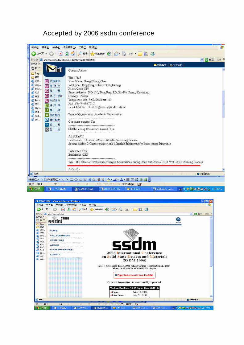
Accepted by 2006 ssdm conference
Accepted by 2006 ssdm conference
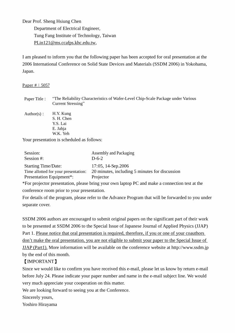
Dear Prof. Sheng Hsiung ChenDepartment of Electrical Engineer,Tung Fang Institute of Technology, [email protected],
I am pleased to inform you that the following paper has been accepted for oral presentation at the2006 International Conference on Solid State Devices and Materials (SSDM 2006) in Yokohama,Japan.
Paper #:5057
Paper Title : “The Reliability Characteristics of Wafer-Level Chip-Scale Package under VariousCurrent Stressing”
Author(s) : H.Y. KungS. H. ChenY.S. LaiE. JahjaW.K. Yeh
Your presentation is scheduled as follows:
Session: Assembly and PackagingSession #: D-6-2
Starting Time/Date: 17:05, 14-Sep.2006Time allotted for your presentation: 20 minutes, including 5 minutes for discussionPresentation Equipment*: Projector
*For projector presentation, please bring your own laptop PC and make a connection test at theconference room prior to your presentation.For details of the program, please refer to the Advance Program that will be forwarded to you underseparate cover.
SSDM 2006 authors are encouraged to submit original papers on the significant part of their workto be presented at SSDM 2006 to the Special Issue of Japanese Journal of Applied Physics (JJAP)Part 1. Please notice that oral presentation is required, therefore, if you or one of your coauthorsdon’t make the oral presentation, you are not eligible to submit your paper to the Special Issue ofJJAP (Part1). More information will be available on the conference website at http://www.ssdm.jpby the end of this month.【IMPORTANT】
Since we would like to confirm you have received this e-mail, please let us know by return e-mailbefore July 24. Please indicate your paper number and name in the e-mail subject line. We wouldvery much appreciate your cooperation on this matter.We are looking forward to seeing you at the Conference.Sincerely yours,Yoshiro Hirayama
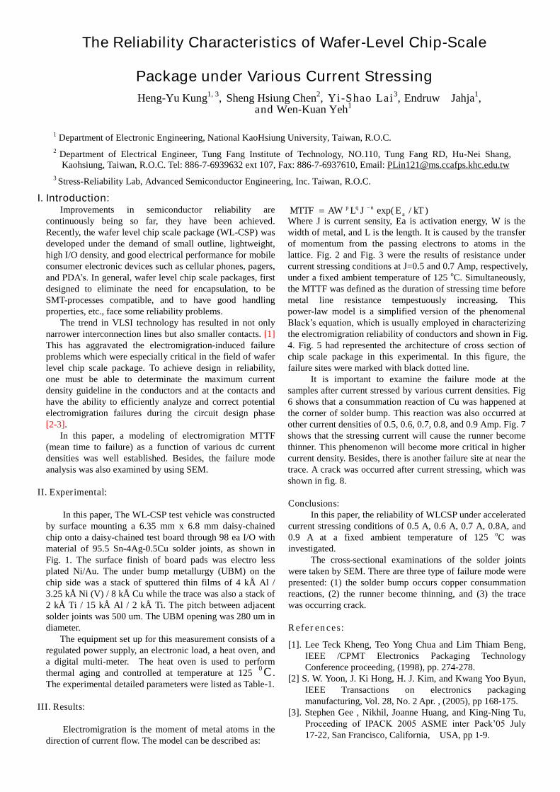
The Reliability Characteristics of Wafer-Level Chip-Scale
Package under Various Current StressingHeng-Yu Kung1, 3, Sheng Hsiung Chen2, Yi-Shao Lai3, Endruw Jahja1,
and Wen-Kuan Yeh1
1 Department of Electronic Engineering, National KaoHsiung University, Taiwan, R.O.C.2 Department of Electrical Engineer, Tung Fang Institute of Technology, NO.110, Tung Fang RD, Hu-Nei Shang,
Kaohsiung, Taiwan, R.O.C. Tel: 886-7-6939632 ext 107, Fax: 886-7-6937610, Email: [email protected] Stress-Reliability Lab, Advanced Semiconductor Engineering, Inc. Taiwan, R.O.C.
I. Introduction:Improvements in semiconductor reliability are
continuously being so far, they have been achieved.Recently, the wafer level chip scale package (WL-CSP) wasdeveloped under the demand of small outline, lightweight,high I/O density, and good electrical performance for mobileconsumer electronic devices such as cellular phones, pagers,and PDA’s.In general, wafer level chip scale packages, firstdesigned to eliminate the need for encapsulation, to beSMT-processes compatible, and to have good handlingproperties, etc., face some reliability problems.
The trend in VLSI technology has resulted in not onlynarrower interconnection lines but also smaller contacts. [1]This has aggravated the electromigration-induced failureproblems which were especially critical in the field of waferlevel chip scale package. To achieve design in reliability,one must be able to determinate the maximum currentdensity guideline in the conductors and at the contacts andhave the ability to efficiently analyze and correct potentialelectromigration failures during the circuit design phase[2-3].
In this paper, a modeling of electromigration MTTF(mean time to failure) as a function of various dc currentdensities was well established. Besides, the failure modeanalysis was also examined by using SEM.
II. Experimental:
In this paper, The WL-CSP test vehicle was constructedby surface mounting a 6.35 mm x 6.8 mm daisy-chainedchip onto a daisy-chained test board through 98 ea I/O withmaterial of 95.5 Sn-4Ag-0.5Cu solder joints, as shown inFig. 1. The surface finish of board pads was electro lessplated Ni/Au. The under bump metallurgy (UBM) on thechip side was a stack of sputtered thin films of 4 kÅ Al /3.25 kÅ Ni (V) / 8 kÅ Cu while the trace was also a stack of2 kÅ Ti / 15 kÅ Al / 2 kÅ Ti. The pitch between adjacentsolder joints was 500 um. The UBM opening was 280 um indiameter.
The equipment set up for this measurement consists of aregulated power supply, an electronic load, a heat oven, anda digital multi-meter. The heat oven is used to performthermal aging and controlled at temperature at 125 C0 .The experimental detailed parameters were listed as Table-1.
III. Results:
Electromigration is the moment of metal atoms in thedirection of current flow. The model can be described as:
)/exp( kTEJLAWMTTF anqp
Where J is current sensity, Ea is activation energy, W is thewidth of metal, and L is the length. It is caused by the transferof momentum from the passing electrons to atoms in thelattice. Fig. 2 and Fig. 3 were the results of resistance undercurrent stressing conditions at J=0.5 and 0.7 Amp, respectively,under a fixed ambient temperature of 125 oC. Simultaneously,the MTTF was defined as the duration of stressing time beforemetal line resistance tempestuously increasing. Thispower-law model is a simplified version of the phenomenalBlack’s equation, which is usually employed in characterizing the electromigration reliability of conductors and shown in Fig.4. Fig. 5 had represented the architecture of cross section ofchip scale package in this experimental. In this figure, thefailure sites were marked with black dotted line.
It is important to examine the failure mode at thesamples after current stressed by various current densities. Fig6 shows that a consummation reaction of Cu was happened atthe corner of solder bump. This reaction was also occurred atother current densities of 0.5, 0.6, 0.7, 0.8, and 0.9 Amp. Fig. 7shows that the stressing current will cause the runner becomethinner. This phenomenon will become more critical in highercurrent density. Besides, there is another failure site at near thetrace. A crack was occurred after current stressing, which wasshown in fig. 8.
Conclusions:In this paper, the reliability of WLCSP under accelerated
current stressing conditions of 0.5 A, 0.6 A, 0.7 A, 0.8A, and0.9 A at a fixed ambient temperature of 125 oC wasinvestigated.
The cross-sectional examinations of the solder jointswere taken by SEM. There are three type of failure mode werepresented: (1) the solder bump occurs copper consummationreactions, (2) the runner become thinning, and (3) the tracewas occurring crack.
References:
[1]. Lee Teck Kheng, Teo Yong Chua and Lim Thiam Beng,IEEE /CPMT Electronics Packaging TechnologyConference proceeding, (1998), pp. 274-278.
[2] S. W. Yoon, J. Ki Hong, H. J. Kim, and Kwang Yoo Byun,IEEE Transactions on electronics packagingmanufacturing, Vol. 28, No. 2 Apr. , (2005), pp 168-175.
[3]. Stephen Gee , Nikhil, Joanne Huang, and King-Ning Tu,Proceeding of IPACK 2005 ASME inter Pack’05 July 17-22, San Francisco, California, USA, pp 1-9.
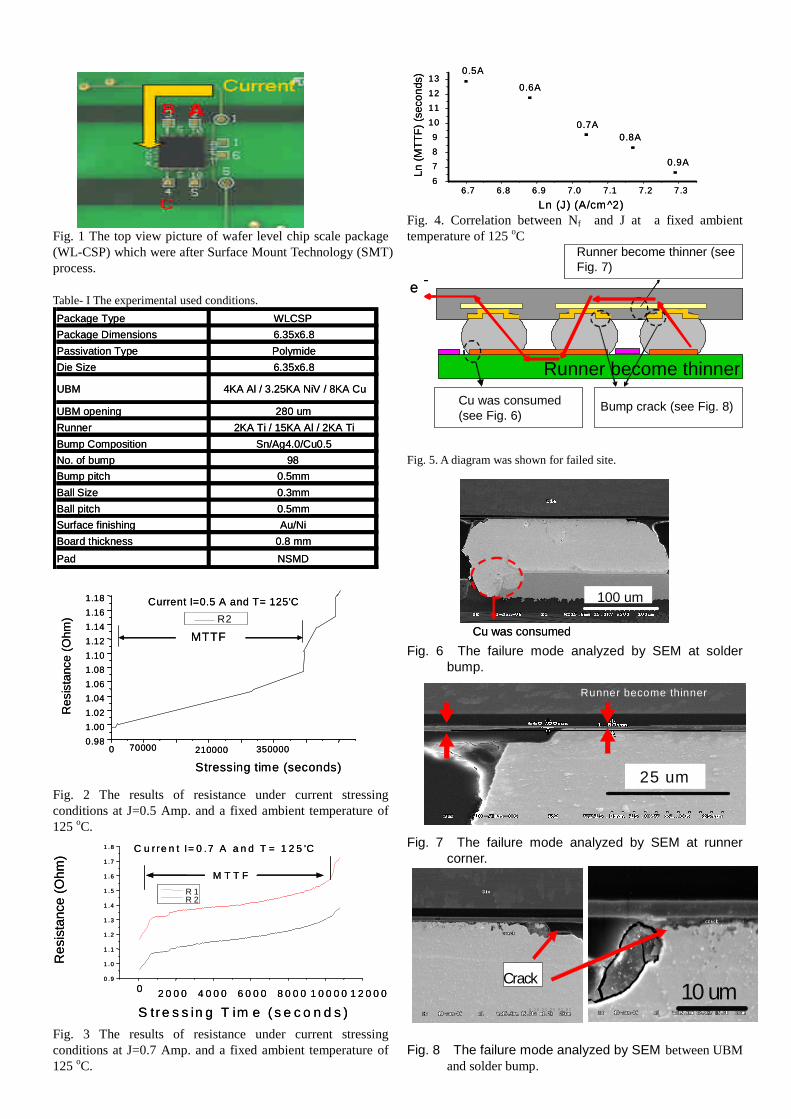
Fig. 1 The top view picture of wafer level chip scale package(WL-CSP) which were after Surface Mount Technology (SMT)process.
Table- I The experimental used conditions.
Fig. 2 The results of resistance under current stressingconditions at J=0.5 Amp. and a fixed ambient temperature of125 oC.
Fig. 3 The results of resistance under current stressingconditions at J=0.7 Amp. and a fixed ambient temperature of125 oC.
Fig. 4. Correlation between Nf and J at a fixed ambienttemperature of 125 oC
Fig. 5. A diagram was shown for failed site.
Fig. 6 The failure mode analyzed by SEM at solderbump.
Fig. 7 The failure mode analyzed by SEM at runnercorner.
Fig. 8 The failure mode analyzed by SEM between UBMand solder bump.
6.7 6.8 6.9 7.0 7.1 7.2 7.36
7
8
9
10
11
12
130.5A
0.6A
0.7A0.8A
0.9A
Ln(M
TT
F)
(sec
onds
)
Ln (J) (A/cm^2)6.7 6.8 6.9 7.0 7.1 7.2 7.3
6
7
8
9
10
11
12
130.5A
0.6A
0.7A0.8A
0.9A
Ln(M
TT
F)
(sec
onds
)
Ln (J) (A/cm^2)
100 um
Cu was consumed
100 um100 um
Cu was consumed
25 um
Runner become thinner
25 um
Runner become thinner
Crack10 um
Crack10 um
MTTF
0 70000 3500000.98
1.00
1.02
1.04
1.06
1.08
1.10
1.12
1.14
1.16
1.18
Res
ista
nce
(Ohm
)
Stressing time (seconds)
R2
Current I=0.5 A and T= 125'C
210000
MTTF
0 70000 3500000.98
1.00
1.02
1.04
1.06
1.08
1.10
1.12
1.14
1.16
1.18
Res
ista
nce
(Ohm
)
Stressing time (seconds)
R2
Current I=0.5 A and T= 125'C
210000
Res
ista
nce
(Ohm
)
0 2 0 0 0 4 0 0 0 6 0 0 0 8 0 0 0 1 0 0 0 0 1 2 0 0 0
0 .9
1 .0
1 .1
1 .2
1 .3
1 .4
1 .5
1 .6
1 .7
1 .8
R 1R 2
C u r re n t I= 0 .7 A a n d T = 1 2 5 'C
S tr e s s in g T im e ( s e c o n d s )
M T T F
Res
ista
nce
(Ohm
)
0 2 0 0 0 4 0 0 0 6 0 0 0 8 0 0 0 1 0 0 0 0 1 2 0 0 0
0 .9
1 .0
1 .1
1 .2
1 .3
1 .4
1 .5
1 .6
1 .7
1 .8
R 1R 2
C u r re n t I= 0 .7 A a n d T = 1 2 5 'C
S tr e s s in g T im e ( s e c o n d s )
M T T F
Package Type WLCSP
Package Dimensions 6.35x6.8
Passivation Type Polymide
Die Size 6.35x6.8
UBM 4KA Al / 3.25KA NiV / 8KA Cu
UBM opening 280 um
Runner 2KA Ti / 15KA Al / 2KA Ti
Bump Composition Sn/Ag4.0/Cu0.5
No. of bump 98Bump pitch 0.5mm
Ball Size 0.3mm
Ball pitch 0.5mm
Surface finishing Au/Ni
Board thickness 0.8 mm
Pad NSMD
Runner become thinner (seeFig. 7)
e -
Bump crack (see Fig. 8)Cu was consumed(see Fig. 6)
Runner become thinner
Runner become thinner (seeFig. 7)
e -
Bump crack (see Fig. 8)Cu was consumed(see Fig. 6)
Runner become thinner


