134
Intel Integrated Graphics Device OpRegion Specification Driver Programmer’s Reference Manual October 1st, 2008 Revision 1.0 Technical queries: [email protected] www.intellinuxgraphics.org

Intel Integrated Graphics Device OpRegion Specification Driver Programmer’s Reference Manual October 1st, 2008 Revision 1.0 Technical queries: [email protected] www.intellinuxgraphics.org

2
Creative Commons License
You are free:
to Share – to copy, distribute, display, and perform the work
Under the following conditions:
Attribution. You must attribute the work in the manner specified by the author or licensor (but not in any way that suggests that they endorse you or your use of the work).
No Derivative Works. You may not alter, transform, or build upon this work.
INFORMATION IN THIS DOCUMENT IS PROVIDED IN CONNECTION WITH INTEL PRODUCTS. NO LICENSE, EXPRESS OR IMPLIED, BY ESTOPPEL OR OTHERWISE, TO ANY INTELLECTUAL PROPERTY RIGHTS IS GRANTED BY THIS DOCUMENT. EXCEPT AS PROVIDED IN INTEL'S TERMS AND CONDITIONS OF SALE FOR SUCH PRODUCTS, INTEL ASSUMES NO LIABILITY WHATSOEVER AND INTEL DISCLAIMS ANY EXPRESS OR IMPLIED WARRANTY, RELATING TO SALE AND/OR USE OF INTEL PRODUCTS INCLUDING LIABILITY OR WARRANTIES RELATING TO FITNESS FOR A PARTICULAR PURPOSE, MERCHANTABILITY, OR INFRINGEMENT OF ANY PATENT, COPYRIGHT OR OTHER INTELLECTUAL PROPERTY RIGHT. UNLESS OTHERWISE AGREED IN WRITING BY INTEL, THE INTEL PRODUCTS ARE NOT DESIGNED NOR INTENDED FOR ANY APPLICATION IN WHICH THE FAILURE OF THE INTEL PRODUCT COULD CREATE A SITUATION WHERE PERSONAL INJURY OR DEATH MAY OCCUR. Intel may make changes to specifications and product descriptions at any time, without notice. Designers must not rely on the absence or characteristics of any features or instructions marked "reserved" or "undefined." Intel reserves these for future definition and shall have no responsibility whatsoever for conflicts or incompatibilities arising from future changes to them. The information here is subject to change without notice. Do not finalize a design with this information. Designers must not rely on the absence or characteristics of any features or instructions marked "reserved" or "undefined." Intel reserves these for future definition and shall have no responsibility whatsoever for conflicts or incompatibilities arising from future changes to them.
Intel and the Intel logo are trademarks or registered trademarks of Intel Corporation or its subsidiaries in the United States and other countries.
*Other names and brands may be claimed as the property of others.
Copyright © 2008, Intel Corporation. All rights reserved.
3
Contents
1 Introduction ....................................................................................................................... 11 1.1 Terminology..........................................................................................................11 1.2 Reference Documents.......................................................................................... 12 1.3 Overview............................................................................................................... 12 1.4 Motivation ............................................................................................................. 13
2 IGD OpRegion Overview ..................................................................................................14 2.1 Introduction...........................................................................................................14 2.2 OpRegion Layout ................................................................................................. 15
2.2.1 OpRegion Header................................................................................. 17 2.2.1.1 Signature ............................................................................. 17 2.2.1.2 Size...................................................................................... 18 2.2.1.3 IGD OpRegion Version........................................................ 19 2.2.1.4 System BIOS Version.......................................................... 21 2.2.1.5 Video BIOS Version............................................................. 21 2.2.1.6 Graphics Driver Version ...................................................... 22 2.2.1.7 Supported Mailboxes........................................................... 24 2.2.1.8 Driver Model ........................................................................ 25
2.3 OpRegion Initialization ......................................................................................... 26 2.3.1 ASLS — ASL Storage........................................................................... 27
2.4 SCI Invocation ......................................................................................................28 2.4.1 SWSCI — Software SCI Register......................................................... 29
3 IGD OpRegion Mailboxes .................................................................................................31 3.1 Mailbox #1: Public ACPI Methods Mailbox .......................................................... 31
3.1.1 Driver Ready .........................................................................................33 3.1.2 Notification Status .................................................................................34 3.1.3 Current Event........................................................................................35 3.1.4 Supported Display Devices ID List ....................................................... 37 3.1.5 Currently Attached Display Devices List............................................... 38 3.1.6 Currently Active Display Devices List ................................................... 40 3.1.7 Next Active Display Devices List .......................................................... 41 3.1.8 ASL Sleep Timeout ............................................................................... 42 3.1.9 Toggle Table Index ............................................................................... 43 3.1.10 Current Hotplug Enable Indicator ......................................................... 44 3.1.11 Current Lid State Indicator.................................................................... 45 3.1.12 Current Docking State Indicator ........................................................... 46 3.1.13 Sx State Resume.................................................................................. 47 3.1.14 ASL Supported Events (EVTS)............................................................. 48 3.1.15 Current OS Notification (CNOT) ........................................................... 50 3.1.16 Driver Status (NRDY) ........................................................................... 51
3.2 Mailbox #2: SWSCI Mailbox................................................................................. 52

4
3.2.1 SWSCI Command................................................................................. 53 3.2.1.1 Command Mode.................................................................. 54 3.2.1.2 Status Mode ........................................................................ 54
3.2.2 SWSCI Parameters .............................................................................. 55 3.2.3 SWSCI Driver Sleep Timeout ............................................................... 55
3.3 Mailbox #3: ASLE Support ................................................................................... 56 3.3.1 Driver Readiness .................................................................................. 57 3.3.2 ASLE Interrupt Command..................................................................... 58 3.3.3 Technology Enabled Indicator .............................................................. 60 3.3.4 Current ALS Luminance Reading......................................................... 61 3.3.5 Requested Backlight Brightness........................................................... 62 3.3.6 Panel Fitting (PFIT)............................................................................... 62 3.3.7 Current Brightness Level ...................................................................... 64 3.3.8 Backlight Brightness Level Duty Cycle Mapping Table ........................ 65 3.3.9 Current Panel Fitting Mode................................................................... 66 3.3.10 Enabled Panel Fitting Modes................................................................ 68 3.3.11 Panel LUT and Identifier ....................................................................... 69 3.3.12 Requested PWM Frequency and Minimum Brightness........................ 70 3.3.13 Color Correction Default Values ........................................................... 71
4 Video BIOS Table .............................................................................................................73 4.1 Background ..........................................................................................................73 4.2 Requirements Summary.......................................................................................74 4.3 VBT Retrieval Methods ........................................................................................ 74 4.4 OpRegion Method ................................................................................................ 75
5 Legacy and Exception Handling ....................................................................................... 76 5.1 No ACPI OpRegion Support................................................................................. 76 5.2 Partial Mailbox support......................................................................................... 76 5.3 Invalid VBT ........................................................................................................... 77
6 Public ACPI Methods ........................................................................................................ 78 6.1 ACPI Requirements..............................................................................................78 6.2 Intel Requirements ...............................................................................................80 6.3 Driver Readiness.................................................................................................. 82 6.4 Display Enumeration ............................................................................................82
6.4.1 Background........................................................................................... 82 6.4.2 System BIOS Display Re-enumeration Triggers .................................. 83 6.4.3 Requirements........................................................................................ 83 6.4.4 Display Enumeration Types.................................................................. 84
6.4.4.1 Operating System Initiated Enumeration ............................ 84 6.4.4.2 System BIOS/Graphics Driver Initiated Enumeration ......... 85 6.4.4.3 User Initiated Enumeration.................................................. 85
6.4.5 Typical Enumeration Flow .................................................................... 86 6.4.6 EDID Reporting..................................................................................... 87
6.5 Display Switch ......................................................................................................87 6.5.1 Background........................................................................................... 87 6.5.2 Requirements Summary ....................................................................... 88 6.5.3 Typical Display Switch Flow ................................................................. 89
7 SWSCI Communication .................................................................................................... 90

5
7.1 SWSCI - The Transport Layer.............................................................................. 90 7.1.1 Software SCI Register .......................................................................... 91
7.1.1.1 Register Interface Service ................................................... 91 7.1.1.2 SMI or SCI Select ................................................................ 92 7.1.1.3 Control Flow on SCI ............................................................ 92
7.2 SWSCI – The Communication Protocol ............................................................... 92 7.2.1 OpRegion Fields ...................................................................................93
7.2.1.1 SCIC .................................................................................... 93 7.2.1.2 PARM .................................................................................. 93
7.2.2 Protocol Overview................................................................................. 94 7.2.2.1 Interface Function................................................................94 7.2.2.2 Interface Sub-Function ........................................................ 94 7.2.2.3 Interface Exit Result ............................................................ 95 7.2.2.4 Interface Override Policy ..................................................... 95
7.2.3 Protocol Descriptions............................................................................ 97 7.2.3.1 Function Description............................................................ 97 7.2.3.2 Sub Function Description .................................................... 97
7.2.4 Protocol Function Details...................................................................... 98 7.2.4.1 Supported Calls ................................................................... 98 7.2.4.2 Requested System Callbacks ............................................. 99 7.2.4.3 Get Boot Display Preferences ...........................................101 7.2.4.4 Get Panel Details............................................................... 105 7.2.4.5 Get TV Standard................................................................ 107
7.2.4.5.1 TV Standard ...................................................... 108 7.2.4.5.2 Video Connector................................................ 110
7.2.4.6 Get Internal Graphics Settings .......................................... 110 7.2.4.7 Get Spread Spectrum Clocks............................................113 7.2.4.8 Supported Callbacks .........................................................114 7.2.4.9 BIOS Post Completion Notification.................................... 116 7.2.4.10 Pre-Hires Set Mode...........................................................117 7.2.4.11 Post-Hires Set Mode ......................................................... 118 7.2.4.12 Display Switch ................................................................... 119 7.2.4.13 Set TV-Standard................................................................ 121 7.2.4.14 Adapter Power State Notification ...................................... 122 7.2.4.15 Display Power State Notification ....................................... 123 7.2.4.16 Set Boot Display Preference ............................................. 125 7.2.4.17 Set Panel Preference ........................................................ 127 7.2.4.18 Switch to Full-Screen ........................................................ 129 7.2.4.19 APM Complete .................................................................. 130 7.2.4.20 Set Spread Spectrum Clocks ............................................131 7.2.4.21 Post VBE/PM Set Power State Notification....................... 132 7.2.4.22 Set PAVP Data .................................................................. 133

6
Figures Figure 2-1 OVER – Bit Field Definition .............................................................................20 Figure 3-1 CEVT – Current Event: Bit Field Definition...................................................... 36 Figure 3-2 CLID – Current Lid State Indicator: Bit Field Definition .................................. 45 Figure 6-1 Display Enumeration Flow............................................................................... 86 Figure 6-2 Display Switch Flow......................................................................................... 89
Tables Table 1-1 Driver and BIOS Communication Methods ...................................................... 13 Table 2-1 OpRegion Memory Layout................................................................................16 Table 2-2 OpRegion Header Layout.................................................................................17 Table 2-3 Signature Field of OpRegion Header ............................................................... 17 Table 2-4 Signature Field of OpRegion Header Details ................................................... 18 Table 2-5 Size Field of OpRegion Header........................................................................ 18 Table 2-6 Size Field of OpRegion Header Details............................................................ 19 Table 2-7 Version Field of OpRegion Header................................................................... 19 Table 2-8 IGD OpRegion Version Field of OpRegion Header Details.............................. 20 Table 2-9 OVER – Version Field Example ....................................................................... 20 Table 2-10 BIOS Version Field of OpRegion Header....................................................... 21 Table 2-11 System BIOS Version Field of OpRegion Header Details.............................. 21 Table 2-12 Video BIOS Version Field of OpRegion Header............................................. 21 Table 2-13 Video BIOS Version Field of OpRegion Header Details ................................ 22 Table 2-14 Graphics Driver Version Field of OpRegion Header ...................................... 22 Table 2-15 Graphics Driver Version Field of OpRegion Header Details .......................... 23 Table 2-16 Supported Mailboxes Field of OpRegion Header........................................... 24 Table 2-17 Supported Mailboxes Field of OpRegion Header Details............................... 24 Table 2-18 Driver Model Field of OpRegion Header ........................................................ 25 Table 2-19 Driver Model Field of OpRegion Header Details ............................................ 26 Table 2-20 ASL Storage ...................................................................................................27 Table 2-21 ASLS Storage Register Layout....................................................................... 28 Table 2-22 SWSCI Register..............................................................................................29 Table 2-23 SWSCI Register Layout.................................................................................. 30 Table 3-1 Mailbox #1 - Public ACPI Methods: Table of Fields ......................................... 31 Table 3-2 Driver Ready..................................................................................................... 33 Table 3-3 Driver Ready Details......................................................................................... 33 Table 3-4 Notification Status.............................................................................................34 Table 3-5 Notification Status Details................................................................................. 34 Table 3-6 Current Event....................................................................................................35 Table 3-7 Current Event Details........................................................................................ 35 Table 3-8 CEVT - Current Event : Valid Values................................................................ 36 Table 3-9 Supported Display Devices .............................................................................. 37 Table 3-10 Supported Display Devices Details ................................................................ 37 Table 3-11 ACPI ID Layout ...............................................................................................37 Table 3-12 Currently Attached Display Devices ............................................................... 38 Table 3-13 Currently Attached Display Devices Details ................................................... 39 Table 3-14 Currently Active Display Devices.................................................................... 40

7
Table 3-15 Currently Active Display Devices Details ....................................................... 40 Table 3-16 Next Active Display Devices........................................................................... 41 Table 3-17 Next Active Display Devices Details............................................................... 41 Table 3-18 ASL Sleep Timeout......................................................................................... 42 Table 3-19 ASL Sleep Timeout Details............................................................................. 42 Table 3-20 Toggle Table Index ......................................................................................... 43 Table 3-21 Toggle Table Index Details ............................................................................. 43 Table 3-22 Current Hotplug Enable Indicator ................................................................... 44 Table 3-23 Current Hotplug Enable Indicator Details ....................................................... 44 Table 3-24 Current Lid State............................................................................................. 45 Table 3-25 Current Lid State Details................................................................................. 45 Table 3-26 CLID – Table of Valid Values ......................................................................... 46 Table 3-27 Current Docking State .................................................................................... 46 Table 3-28 Current Docking State Details ........................................................................ 47 Table 3-29 Sx State Resume............................................................................................47 Table 3-30 Sx State Resume Details................................................................................ 48 Table 3-31 ASL Supported Events ...................................................................................48 Table 3-32 ASL Supported Events Details ....................................................................... 49 Table 3-33 EVTS – ASL Supported Events: Valid Values................................................ 49 Table 3-34 Current OS Notification................................................................................... 50 Table 3-35 Current OS Notification Details....................................................................... 50 Table 3-36: CNOT - Current OS Notification: Value Values............................................. 50 Table 3-37 Driver Status ...................................................................................................51 Table 3-38 Driver Status Details ....................................................................................... 52 Table 3-39: NRDY-Driver Status: Valid Values ................................................................ 52 Table 3-40 Mailbox #2 - SWSCI : Table of Fields............................................................. 53 Table 3-41 SWSCI Command .......................................................................................... 53 Table 3-42 SWSCI Parameters ........................................................................................55 Table 3-43 SWSCI Driver Sleep Timeout ......................................................................... 55 Table 3-44 Mailbox #3 - ASLE Support: Table of Fields................................................... 56 Table 3-45 Driver Readiness ............................................................................................ 57 Table 3-46 Driver Readiness Details ................................................................................ 58 Table 3-47 ASLE Command Details .................................................................................59 Table 3-48 Technology Enabled Details........................................................................... 60 Table 3-49 ALS Luminance Details .................................................................................. 61 Table 3-50 Requested Backlight Brightness Details ........................................................ 62 Table 3-51 Panel fitting .....................................................................................................63 Table 3-52 Panel Fitting Details........................................................................................ 63 Table 3-53 Current Brightness Level ................................................................................ 64 Table 3-54 Current Brightness Level Detail...................................................................... 64 Table 3-55 Backlight Brightness Level Duty Cycle Mapping ............................................ 65 Table 3-56 Backlight Brightness Duty Cycle Mapping Table Detail ................................. 66 Table 3-57 Current Panel Fitting Mode............................................................................. 66 Table 3-58 Current Panel Fitting Mode Details................................................................. 67 Table 3-59 Enabled Panel Fitting Modes.......................................................................... 68 Table 3-60 Enabled Panel Fitting Modes Detail ............................................................... 68 Table 3-61 Panel and LUT Identifier ................................................................................. 69 Table 3-62 Panel Identifier Detail......................................................................................70 Table 3-63 Requested PWM Frequency .......................................................................... 70 Table 3-64 Requested PWM Frequency and Minimum Brightness Details ..................... 71 Table 3-65 Color Correction Default Values Details......................................................... 72
8
Table 4-1 Video BIOS Table ............................................................................................. 73 Table 4-2 Video BIOS Table Requirements Summary..................................................... 74 Table 6-1 ACPI Video Extension Requirements............................................................... 78 Table 6-2 Intel Requirements for System BIOS & Graphics Driver .................................. 80 Table 7-1 SWSCI Register................................................................................................91 Table 7-2 Function Call Exit Result................................................................................... 91 Table 7-3 Function Call Exit Result................................................................................... 92 Table 7-4 SCI Command Field ......................................................................................... 93 Table 7-5 SCI Parameters ................................................................................................ 94 Table 7-6 Protocol Interface Function Codes ................................................................... 94 Table 7-7 Function Call Exit Result................................................................................... 94 Table 7-8 Function Call Exit Result................................................................................... 95 Table 7-9 SCI Command Fields........................................................................................96 Table 7-10 Protocol Interface Function Codes ................................................................. 97 Table 7-11 Protocol Interface Sub-function Codes........................................................... 97 Table 7-12 SWSCI Mailbox, SCIC Offset ......................................................................... 98 Table 7-13 SWSCI Mailbox, SCIC Offset ......................................................................... 99 Table 7-14 SWSCI Mailbox, SCIC Offset ......................................................................... 99 Table 7-15 SWSCI Mailbox, SCIC Offset .......................................................................100 Table 7-16 SWSCI Mailbox, PARM Offset – Bit Mask of Requested Callbacks ............ 100 Table 7-17 SWSCI Mailbox, SCIC Offset .......................................................................101 Table 7-18 SWSCI Mailbox, PARM Offset – Display Port Device Type Mask ............... 102 Table 7-19 SWSCI Mailbox, SCIC Offset .......................................................................102 Table 7-20 SWSCI Mailbox, PARM Offset – Boot Display Preference .......................... 103 Table 7-21 SWSCI Mailbox, SCIC Offset .......................................................................105 Table 7-22 SWSCI Mailbox, PARM Offset – Display Port Device Type Mask ............... 105 Table 7-23 SWSCI Mailbox, SCIC Offset .......................................................................105 Table 7-24 SWSCI Mailbox, PARM Offset – Panel Details ............................................ 106 Table 7-25 SWSCI Mailbox, SCIC Offset .......................................................................107 Table 7-26 SWSCI Mailbox, PARM Offset – TV Number ............................................... 107 Table 7-27 SWSCI Mailbox, SCIC Offset .......................................................................107 Table 7-28 SWSCI Mailbox, PARM Offset – Return the TV Standard ........................... 108 Table 7-29 S-Video/Composite/SCART Standard Formats ........................................... 108 Table 7-30 Component/D-connector Standard Formats ................................................ 109 Table 7-31 Video Connector ...........................................................................................110 Table 7-32 SWSCI Mailbox, SCIC Offset .......................................................................110 Table 7-33 SWSCI Mailbox, SCIC Offset .......................................................................111 Table 7-34 SWSCI Mailbox, PARM Offset – GMCH Configuration................................ 111 Table 7-35 DVMT Graphics Memory Size’s Per Version .............................................. 112 Table 7-36 DVMT 4.0 Options ........................................................................................113 Table 7-37 SWSCI Mailbox, SCIC Offset .......................................................................113 Table 7-38 SWSCI Mailbox, SCIC Offset .......................................................................113 Table 7-39 SWSCI Mailbox, PARM Offset – Spread Spectrum Clock ........................... 114 Table 7-40 SWSCI Mailbox, SCIC Offset .......................................................................114 Table 7-41 SWSCI Mailbox, SCIC Offset .......................................................................115 Table 7-42 SWSCI Mailbox, PARM Offset – Bit Mask of Requested Callbacks ............ 115 Table 7-43 SWSCI Mailbox, SCIC Offset .......................................................................116 Table 7-44 SWSCI Mailbox, SCIC Offset .......................................................................117 Table 7-45 SWSCI Mailbox, SCIC Offset .......................................................................117 Table 7-46 SWSCI Mailbox, PARM Offset – Mode Information ..................................... 117 Table 7-47 SWSCI Mailbox, SCIC Offset .......................................................................118 Table 7-48 SWSCI Mailbox, SCIC Offset .......................................................................118
9
Table 7-49 SWSCI Mailbox, PARM Offset – Mode Information ..................................... 118 Table 7-50 SWSCI Mailbox, SCIC Offset .......................................................................119 Table 7-51 SWSCI Mailbox, SCIC Offset .......................................................................119 Table 7-52 SWSCI Mailbox, PARM Offset – Display Switch Information....................... 120 Table 7-53 SWSCI Mailbox, SCIC Offset .......................................................................121 Table 7-54 SWSCI Mailbox, SCIC Offset .......................................................................121 Table 7-55 SWSCI Mailbox, PARM Offset – TV Format ................................................ 121 Table 7-56 SWSCI Mailbox, SCIC Offset – TV Format .................................................. 122 Table 7-57 SWSCI Mailbox, SCIC Offset .......................................................................122 Table 7-58 SWSCI Mailbox, PARM Offset – Adapter Power State ................................ 122 Table 7-59 SWSCI Mailbox, SCIC Offset .......................................................................123 Table 7-60 SWSCI Mailbox, SCIC Offset .......................................................................123 Table 7-61 SWSCI Mailbox, PARM Offset – Display Power State................................. 124 Table 7-62 SWSCI Mailbox, SCIC Offset .......................................................................124 Table 7-63 SWSCI Mailbox, SCIC Offset .......................................................................125 Table 7-64 SWSCI Mailbox, PARM Offset – TV Format ................................................ 126 Table 7-65 SWSCI Mailbox, SCIC Offset .......................................................................127 Table 7-66 SWSCI Mailbox, SCIC Offset .......................................................................127 Table 7-67 SWSCI Mailbox, PARM Offset – Panel Preference ..................................... 128 Table 7-68 SWSCI Mailbox, SCIC Offset .......................................................................128 Table 7-69 SWSCI Mailbox, SCIC Offset .......................................................................129 Table 7-70 SWSCI Mailbox, PARM Offset – Internal Graphics Preference ................... 129 Table 7-71 SWSCI Mailbox, SCIC Offset .......................................................................129 Table 7-72 SWSCI Mailbox, SCIC Offset .......................................................................130 Table 7-73 SWSCI Mailbox, PARM Offset – Internal Graphics Preference ................... 130 Table 7-74 SWSCI Mailbox, SCIC Offset .......................................................................130 Table 7-75 SWSCI Mailbox, SCIC Offset .......................................................................131 Table 7-76 SWSCI Mailbox, PARM Offset – Internal Graphics Preference ................... 131 Table 7-77 SWSCI Mailbox, SCIC Offset .......................................................................131 Table 7-78 SWSCI Mailbox, SCIC Offset .......................................................................132 Table 7-79 SWSCI Mailbox, PARM Offset – Internal Graphics Preference ................... 132 Table 7-80 SWSCI Mailbox, SCIC Offset – Internal Graphics Preference..................... 132 Table 7-81 SWSCI Mailbox, SCIC Offset .......................................................................133 Table 7-82 SWSCI Mailbox, PARM Offset......................................................................133 Table 7-83 SWSCI Mailbox, SCIC Offset .......................................................................133 Table 7-84 SWSCI Mailbox, SCIC Offset .......................................................................134
10
Revision History Revision Number
Description Author Revision Date
1.0 Initial release jbarnes 8/4/2008
Introduction
11
1 Introduction
1.1 Terminology Term Description
ACPI Advanced Configuration and Power Interface
ADD Advanced Digital Display
AML ACPI Machine Language
ASL ACPI Source Language
ASLS ASL Storage Register
ASLE ASL Event
BIOS Basic Input/Output System
BMP BIOS Modification Program – Use to update BIOS data and features in object code without recompiling
C-Spec Component Specification
DDC Display Data Channel – VESA standard used to retrieve EDID data from a monitor
EFP External Flat Panel
EDID Extended Display Identification Data – monitor data that describes the monitor characteristics
GMCH Graphics Memory Controller Hub
IBV Independent BIOS Vendor
LDDM Longhorn Device Driver Model
LFP Local Flat Panel, normally used on mobile platforms only
MBI Modular BIOS Interface
NVS Non Volatile Storage
OEM Original Equipment Manufacturer
POST Power On Self-Test – chipset initialization code
Introduction
12
Term Description
SBIOS See System BIOS
SDVO Serial Digital Video Out
SCI System Control Interrupt
SMM System Management Mode
SPD Serial Presence Data
SWSCI Software SCI
SSRW Software Scratch Read Write
SMI System Management Interrupt
SMM System Management Mode
System BIOS Software built into the platform, often in flash RAM
1.2 Reference Documents Document Revision Document No./
Location
Advanced Configuration and Power Interface Specification
2.0c, 3.0 http://www.acpi.info/
RS – ACPI _DOD IDs for Intel® Integrated Graphics Software Interface Specification
0.52 http://www.intel.com/
1.3 Overview The Intel graphics driver stack is composed of several different modules: kernel drivers, user level drivers, the video BIOS, system BIOS, and pre-programmed firmware tables. Communication between these various components is complex and varied. The kernel and user level drivers communicate through well defined APIs and ABIs, provided by the operating system. Historically, interaction with the video BIOS and system BIOS has been less standardized, involving several ACPI video extension revisions and numerous platform-specific interfaces, reducing driver portability and reliability, and increasing complexity. This specification describes a scheme intended to replace those obtuse and incompatible methods with a single, well defined, ACPI-based mechanism.
Introduction
13
1.4 Motivation As mentioned in the overview, communication between video drivers and the system firmware has been highly platform-dependent in the past, involving several different methods, described in Table 1-1 Driver and BIOS Communication Methods .
Table 1-1 Driver and BIOS Communication Methods
Interface Description Function
SMI System management interrupt
Invokes SMM code to interact with system firmware.
INT 10h Software interrupt 10h Invokes a real mode software interrupt to communicate with the video BIOS.
MBI Modular BIOS interface Used to communicate information to the graphics driver.
Video BIOS shadow
Memory range at 0xc0000 Location of Video BIOS and memory for inter-module communication.
With the development of new technologies and implementation techniques in deployed operating systems, it has become increasingly difficult to use the above methods for reliable intermodule communication. Several limitations are evident:
1. SMIs have several major problems, exacerbated by recent advances in processor technology
2. INT 10h is not always possible (due to LT or OS restrictions)
3. MBI is not always present and provides limited functionality
4. The video BIOS shadow is not always available
SMIs are particularly problematic since they switch the processor into system management mode (SMM), which has a high context switch cost (1). The transition to SMM is also invisible to the OS and may involve large amounts of processing before resuming normal operation. This can lead to bad behavior like video playback skipping, network packet loss due to timeouts, and missed deadlines for OS timers, which require high precision.
Additionally, changes made to the video hardware during SMM processing can ultimately affect system stability. Certain changes (for instance changing pipe configuration or clock settings) may be incompatible with subsequent programming done by the OS video driver, causing the system to hang. For this reason, it makes sense for a single piece of software to control the video hardware. This ensures consistency and correctness, and simplifies the process of finding and fixing problems when they occur.
1 In typical SMM flows, the interrupted processor sends an SMI to every other processor in the system. Actual SMM processing won’t occur until all other processors have responded to the interrupt and acknowledged the original processor’s SMI. As processor counts increase, this “rendezvous” time can become a significant problem, exacerbating the processing delay issues described above.

IGD OpRegion Overview
14
2 IGD OpRegion Overview
2.1 Introduction Due to the problems outlined in section 1.4 of this document, the ACPI IGD OpRegion interface is intended to replace the various intermodule communication schemes described above, particularly the INT 10h and SMI mechanisms.
However, any replacement must preserve the advantages of the SMM deployment model, namely that OEMs and IBVs can provide proprietary code linked into the platform at build time, which allows for platform differentiation and flexibility.
In platforms supporting the ACPI IGD OpRegion method, the SMI mechanism for the graphics driver-to-system firmware communication is replaced by the System Control Interrupt (SCI) mechanism. It retains the advantages of the SMI/SMM deployment model, but has none of the disadvantages.
IGD OpRegion Overview
15
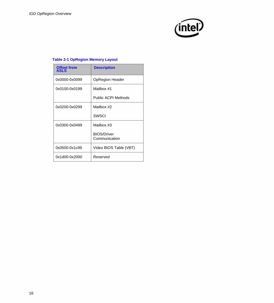
2.2 OpRegion Layout The following table describes the layout of the 8kb OpRegion. Details on each segment can be found below. The OpRegion itself is located somewhere in the low 32 bit memory space. See ASLS — ASL Storage for details on locating the OpRegion.
IGD OpRegion Overview
16
Table 2-1 OpRegion Memory Layout
Offset from ASLS
Description
0x0000-0x0099 OpRegion Header
0x0100-0x0199 Mailbox #1
Public ACPI Methods
0x0200-0x0299 Mailbox #2
SWSCI
0x0300-0x0499 Mailbox #3
BIOS/Driver Communication
0x0500-0x1c99 Video BIOS Table (VBT)
0x1d00-0x2000 Reserved
IGD OpRegion Overview
17
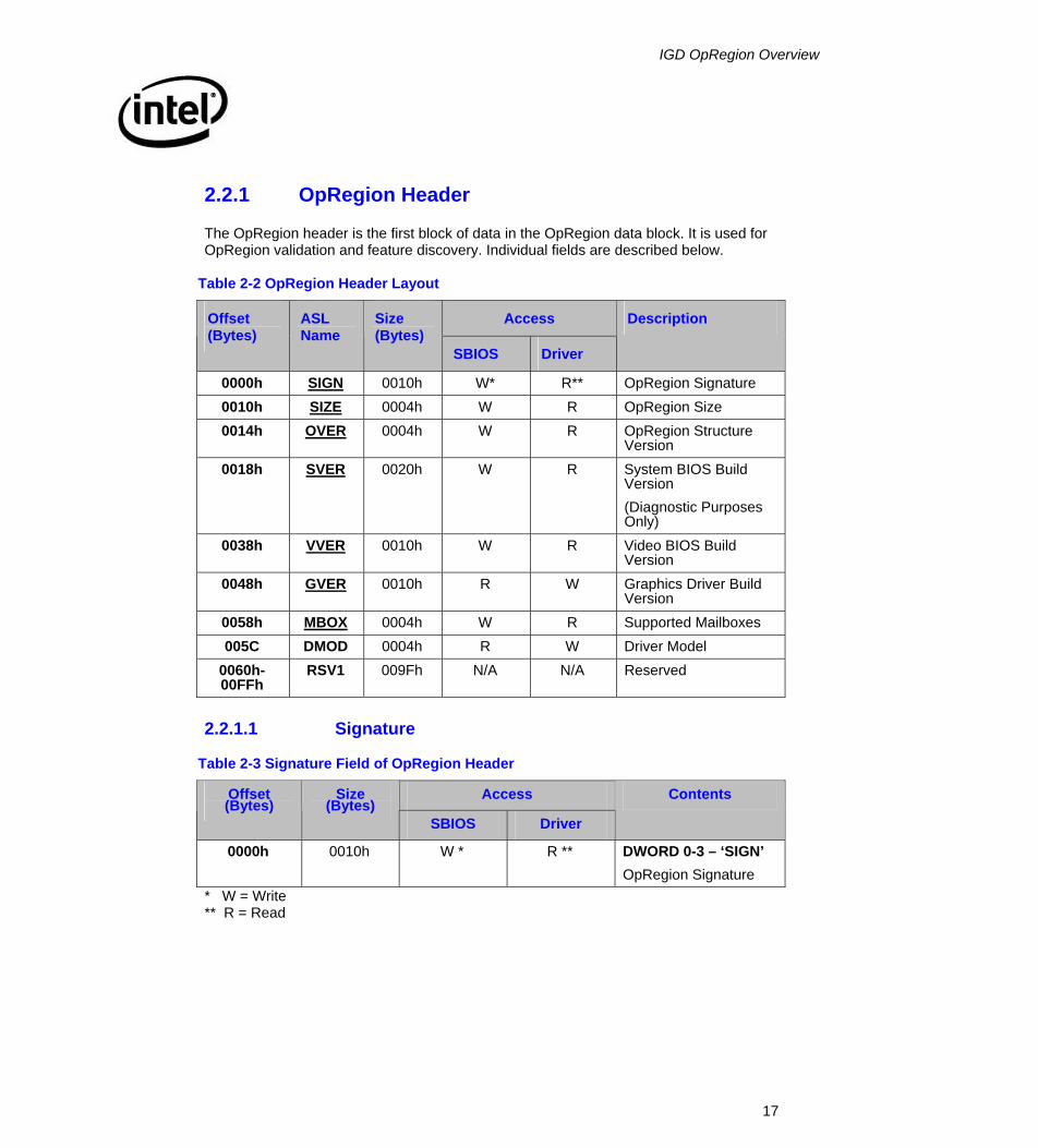
2.2.1 OpRegion Header
The OpRegion header is the first block of data in the OpRegion data block. It is used for OpRegion validation and feature discovery. Individual fields are described below.
Table 2-2 OpRegion Header Layout
Access Offset (Bytes)
ASL Name
Size (Bytes)
SBIOS Driver
Description
0000h SIGN 0010h W* R** OpRegion Signature 0010h SIZE 0004h W R OpRegion Size 0014h OVER 0004h W R OpRegion Structure
Version 0018h SVER 0020h W R System BIOS Build
Version (Diagnostic Purposes Only)
0038h VVER 0010h W R Video BIOS Build Version
0048h GVER 0010h R W Graphics Driver Build Version
0058h MBOX 0004h W R Supported Mailboxes 005C DMOD 0004h R W Driver Model
0060h-00FFh
RSV1 009Fh N/A N/A Reserved
2.2.1.1 Signature
Table 2-3 Signature Field of OpRegion Header
Access Offset (Bytes)
Size (Bytes)
SBIOS Driver
Contents
0000h 0010h W * R ** DWORD 0-3 – ‘SIGN’ OpRegion Signature
* W = Write ** R = Read
IGD OpRegion Overview
18
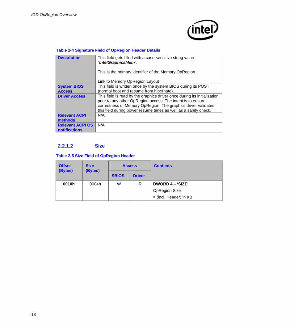
Table 2-4 Signature Field of OpRegion Header Details
Description This field gets filled with a case-sensitive string value “IntelGraphicsMem”. This is the primary identifier of the Memory OpRegion. Link to Memory OpRegion Layout
System BIOS Access
This field is written once by the system BIOS during its POST (normal boot and resume from hibernate).
Driver Access This field is read by the graphics driver once during its initialization, prior to any other OpRegion access. The intent is to ensure correctness of Memory OpRegion. The graphics driver validates this field during power resume times as well as a sanity check.
Relevant ACPI methods
N/A
Relevant ACPI OS notifications
N/A
2.2.1.2 Size
Table 2-5 Size Field of OpRegion Header
Access Offset (Bytes)
Size (Bytes)
SBIOS Driver
Contents
0010h 0004h W R DWORD 4 – ‘SIZE’ OpRegion Size = (incl. Header) in KB

IGD OpRegion Overview
19
Table 2-6 Size Field of OpRegion Header Details
Description This field is filled with the size, in KB, of the entire OpRegion structure (including header). The size field should match the structure definition corresponding to its version indicated by OVER. If the size field is invalid, graphics driver will stop using OpRegion for any purpose and revert back to legacy methods of interacting with system firmware.
System BIOS Access
This field is written once by the system BIOS during its POST (normal boot and resume from hibernate).
Driver Access This field is read by the graphics driver once during its initialization while in the process of Memory OpRegion validation. The intent is to make sure the Memory OpRegion is correct. The graphics driver validates this field during power resume times as well as a sanity check.
Relevant ACPI Methods
N/A
Relevant ACPI OS Notifications
N/A
2.2.1.3 IGD OpRegion Version
Table 2-7 Version Field of OpRegion Header
Access Offset (Bytes)
Size (Bytes)
SBIOS Driver
Contents
0014h 0004h W R DWORD 5 – ‘OVER’ OpRegion Structure Version
IGD OpRegion Overview
20
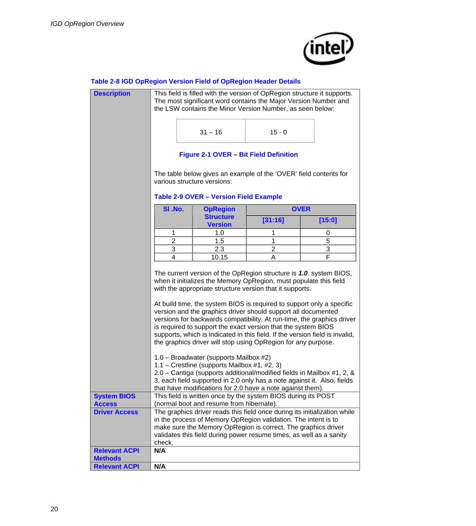
Table 2-8 IGD OpRegion Version Field of OpRegion Header Details
Description This field is filled with the version of OpRegion structure it supports. The most significant word contains the Major Version Number and the LSW contains the Minor Version Number, as seen below:
Figure 2-1 OVER – Bit Field Definition
The table below gives an example of the ‘OVER’ field contents for various structure versions:
Table 2-9 OVER – Version Field Example
OVER Sl .No. OpRegion Structure Version [31:16] [15:0]
1 1.0 1 0 2 1.5 1 5 3 2.3 2 3 4 10.15 A F
The current version of the OpRegion structure is 1.0. system BIOS, when it initializes the Memory OpRegion, must populate this field with the appropriate structure version that it supports.
At build time, the system BIOS is required to support only a specific version and the graphics driver should support all documented versions for backwards compatibility. At run-time, the graphics driver is required to support the exact version that the system BIOS supports, which is indicated in this field. If the version field is invalid, the graphics driver will stop using OpRegion for any purpose.
1.0 – Broadwater (supports Mailbox #2) 1.1 – Crestline (supports Mailbox #1, #2, 3) 2.0 – Cantiga (supports additional/modified fields in Mailbox #1, 2, & 3, each field supported in 2.0 only has a note against it. Also, fields that have modifications for 2.0 have a note against them).
System BIOS Access
This field is written once by the system BIOS during its POST (normal boot and resume from hibernate).
Driver Access The graphics driver reads this field once during its initialization while in the process of Memory OpRegion validation. The intent is to make sure the Memory OpRegion is correct. The graphics driver validates this field during power resume times, as well as a sanity check.
Relevant ACPI Methods
N/A
Relevant ACPI N/A
15 - 0 31 – 16
IGD OpRegion Overview
21
OS Notifications
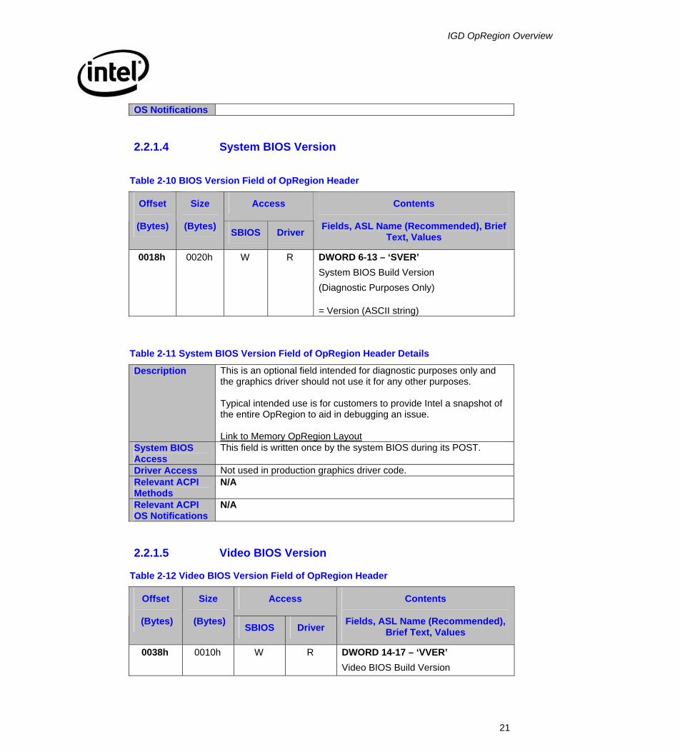
2.2.1.4 System BIOS Version
Table 2-10 BIOS Version Field of OpRegion Header
Access Offset
(Bytes)
Size
(Bytes) SBIOS Driver
Contents
Fields, ASL Name (Recommended), Brief Text, Values
0018h 0020h W R DWORD 6-13 – ‘SVER’ System BIOS Build Version (Diagnostic Purposes Only)
= Version (ASCII string)
Table 2-11 System BIOS Version Field of OpRegion Header Details
Description This is an optional field intended for diagnostic purposes only and the graphics driver should not use it for any other purposes.
Typical intended use is for customers to provide Intel a snapshot of the entire OpRegion to aid in debugging an issue. Link to Memory OpRegion Layout
System BIOS Access
This field is written once by the system BIOS during its POST.
Driver Access Not used in production graphics driver code. Relevant ACPI Methods
N/A
Relevant ACPI OS Notifications
N/A
2.2.1.5 Video BIOS Version
Table 2-12 Video BIOS Version Field of OpRegion Header
Access Offset
(Bytes)
Size
(Bytes) SBIOS Driver
Contents
Fields, ASL Name (Recommended), Brief Text, Values
0038h 0010h W R DWORD 14-17 – ‘VVER’ Video BIOS Build Version

IGD OpRegion Overview
22
Access Offset
(Bytes)
Size
(Bytes) SBIOS Driver
Contents
Fields, ASL Name (Recommended), Brief Text, Values
= Version (ASCII string)
Table 2-13 Video BIOS Version Field of OpRegion Header Details
Description This field is filled with the version of video BIOS (when IGD is primary or secondary) and the intent is for Intel CUI control panel application to display the video BIOS version. This could also be used for diagnostic purposes to aid debugging. Link to Memory OpRegion Layout
System BIOS Access
This field is written once by the system BIOS during its POST (normal boot and resume from hibernate).
Driver Access The graphics driver reads this field upon request from Intel CUI to determine video BIOS information.
Relevant ACPI Methods
N/A
Relevant ACPI OS Notifications
N/A
2.2.1.6 Graphics Driver Version
Table 2-14 Graphics Driver Version Field of OpRegion Header
Access Offset
(Bytes)
Size
(Bytes) SBIOS Driver
Contents
Fields, ASL Name (Recommended), Brief Text,
Values
0048h 0010h R W DWORD 18-21 – ‘GVER’ Graphics Driver Build Version = Version (ASCII string)
IGD OpRegion Overview
23
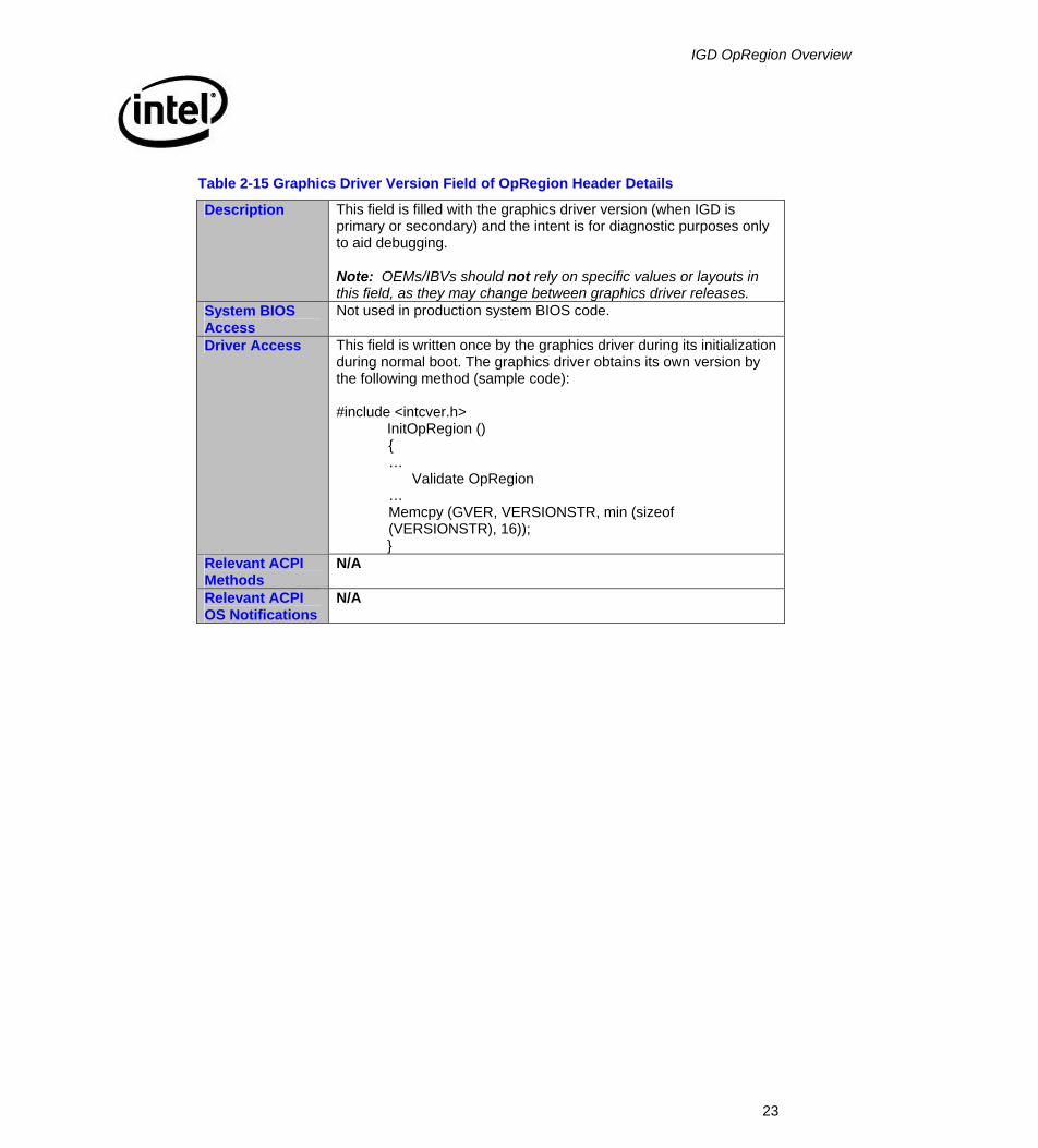
Table 2-15 Graphics Driver Version Field of OpRegion Header Details
Description This field is filled with the graphics driver version (when IGD is primary or secondary) and the intent is for diagnostic purposes only to aid debugging.
Note: OEMs/IBVs should not rely on specific values or layouts in this field, as they may change between graphics driver releases.
System BIOS Access
Not used in production system BIOS code.
Driver Access This field is written once by the graphics driver during its initialization during normal boot. The graphics driver obtains its own version by the following method (sample code):
#include <intcver.h>
InitOpRegion () { …
Validate OpRegion … Memcpy (GVER, VERSIONSTR, min (sizeof (VERSIONSTR), 16)); }
Relevant ACPI Methods
N/A
Relevant ACPI OS Notifications
N/A
IGD OpRegion Overview
24
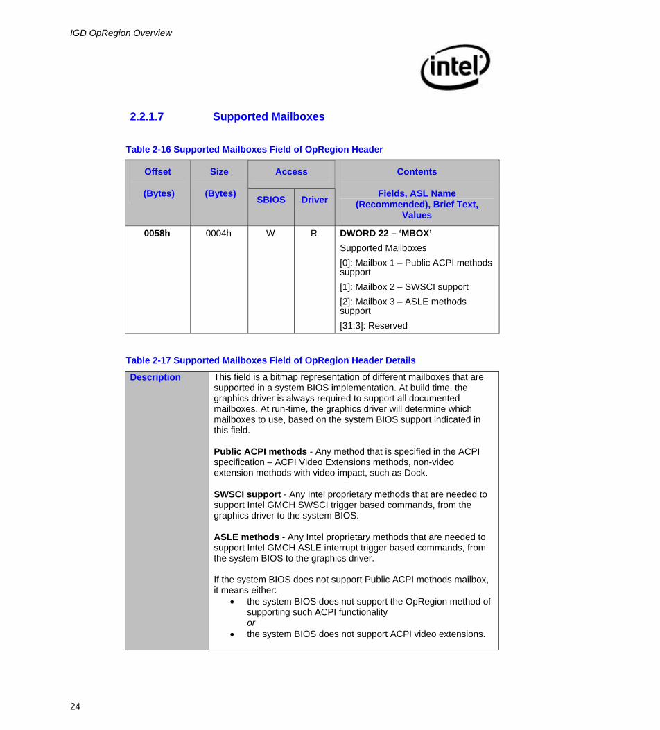
2.2.1.7 Supported Mailboxes
Table 2-16 Supported Mailboxes Field of OpRegion Header
Access Offset
(Bytes)
Size
(Bytes) SBIOS Driver
Contents
Fields, ASL Name (Recommended), Brief Text,
Values
0058h 0004h W R DWORD 22 – ‘MBOX’ Supported Mailboxes [0]: Mailbox 1 – Public ACPI methods support [1]: Mailbox 2 – SWSCI support [2]: Mailbox 3 – ASLE methods support [31:3]: Reserved
Table 2-17 Supported Mailboxes Field of OpRegion Header Details
Description This field is a bitmap representation of different mailboxes that are supported in a system BIOS implementation. At build time, the graphics driver is always required to support all documented mailboxes. At run-time, the graphics driver will determine which mailboxes to use, based on the system BIOS support indicated in this field.
Public ACPI methods - Any method that is specified in the ACPI specification – ACPI Video Extensions methods, non-video extension methods with video impact, such as Dock.
SWSCI support - Any Intel proprietary methods that are needed to support Intel GMCH SWSCI trigger based commands, from the graphics driver to the system BIOS.
ASLE methods - Any Intel proprietary methods that are needed to support Intel GMCH ASLE interrupt trigger based commands, from the system BIOS to the graphics driver.
If the system BIOS does not support Public ACPI methods mailbox, it means either:
• the system BIOS does not support the OpRegion method of supporting such ACPI functionality or
• the system BIOS does not support ACPI video extensions.
IGD OpRegion Overview
25
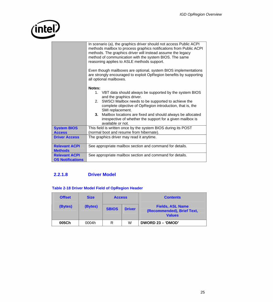
In scenario (a), the graphics driver should not access Public ACPI methods mailbox to process graphics notifications from Public ACPI methods. The graphics driver will instead assume the legacy method of communication with the system BIOS. The same reasoning applies to ASLE methods support.
Even though mailboxes are optional, system BIOS implementations are strongly encouraged to exploit OpRegion benefits by supporting all optional mailboxes.
Notes:
1. VBT data should always be supported by the system BIOS and the graphics driver.
2. SWSCI Mailbox needs to be supported to achieve the complete objective of OpRegion introduction, that is, the SMI replacement.
3. Mailbox locations are fixed and should always be allocated irrespective of whether the support for a given mailbox is available or not.
System BIOS Access
This field is written once by the system BIOS during its POST (normal boot and resume from hibernate).
Driver Access The graphics driver may read it anytime.
Relevant ACPI Methods
See appropriate mailbox section and command for details.
Relevant ACPI OS Notifications
See appropriate mailbox section and command for details.
2.2.1.8 Driver Model
Table 2-18 Driver Model Field of OpRegion Header
Access Offset
(Bytes)
Size
(Bytes) SBIOS Driver
Contents
Fields, ASL Name (Recommended), Brief Text,
Values
005Ch 0004h R W DWORD 23 – ‘DMOD’

IGD OpRegion Overview
26
Table 2-19 Driver Model Field of OpRegion Header Details
Description This field indicates the type or model of graphics driver currently loaded. The graphics driver will update this field once the driver is successfully loaded. The BIOS can read this field to make a decision based on the type of graphics driver loaded. On driver unload, the graphics driver needs to make DMOD = 0, to indicate to the system BIOS that no graphics driver is loaded now.
Note: This field is supported from OpRegion Version(refer OVER) = 2.0 onwards.
Valid Values 00h - The graphics driver is not loaded. 01h - The XPDM driver is loaded. 02h - The WDDM driver is loaded. 03h - The Linux driver is loaded All other values are reserved.
System BIOS Access
The system BIOS can read this field any time.
Driver Access The graphics driver will write to this field on driver load/unload. Relevant ACPI Methods
See appropriate mailbox section and command for details.
Relevant ACPI OS Notifications
See appropriate mailbox section and command for details.
2.3 OpRegion Initialization At boot time, the system firmware is responsible for creating the ACPI IGD OpRegion and loading its base address into the appropriate chipset register. SCI handlers are written in ASL and compiled and linked into the system firmware. Additionally, SCI methods are executed in OS context, rather than SMM context, eliminating the SMI/SMM problems outlined above.
Once the OpRegion has been allocated and initialized, the system firmware is responsible for writing its base address into the ASLS register of the GMCH.
IGD OpRegion Overview
27
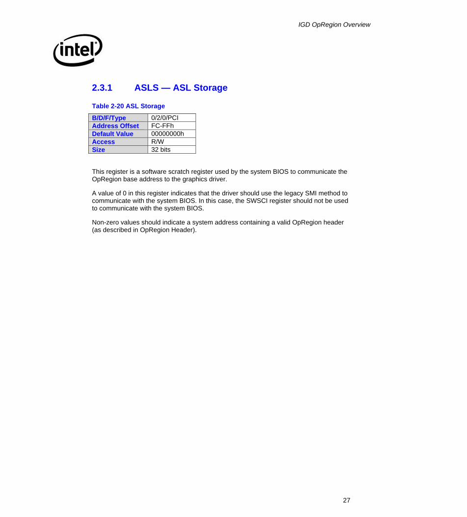
2.3.1 ASLS — ASL Storage
Table 2-20 ASL Storage
B/D/F/Type 0/2/0/PCI Address Offset FC-FFh Default Value 00000000h Access R/W Size 32 bits
This register is a software scratch register used by the system BIOS to communicate the OpRegion base address to the graphics driver.
A value of 0 in this register indicates that the driver should use the legacy SMI method to communicate with the system BIOS. In this case, the SWSCI register should not be used to communicate with the system BIOS.
Non-zero values should indicate a system address containing a valid OpRegion header (as described in OpRegion Header).
IGD OpRegion Overview
28
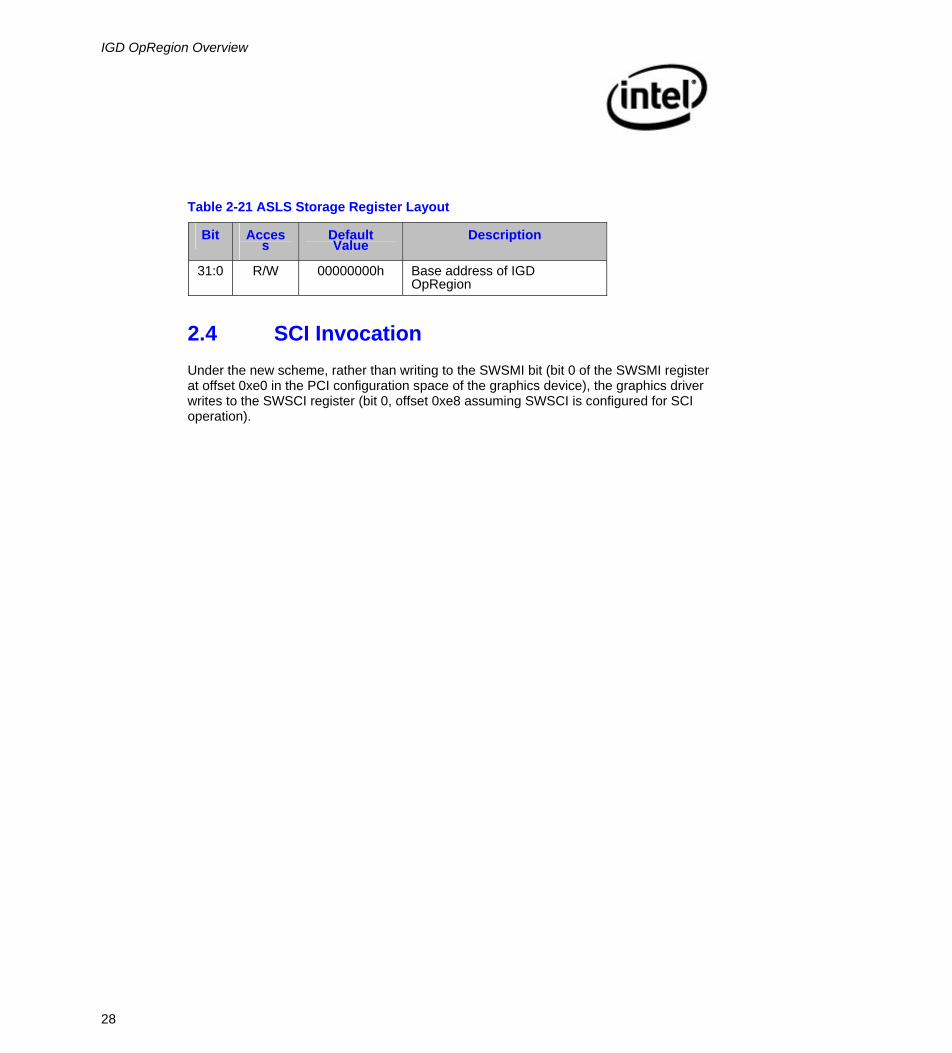
Table 2-21 ASLS Storage Register Layout
Bit Access
Default Value
Description
31:0 R/W 00000000h Base address of IGD OpRegion
2.4 SCI Invocation Under the new scheme, rather than writing to the SWSMI bit (bit 0 of the SWSMI register at offset 0xe0 in the PCI configuration space of the graphics device), the graphics driver writes to the SWSCI register (bit 0, offset 0xe8 assuming SWSCI is configured for SCI operation).
IGD OpRegion Overview
29
2.4.1 SWSCI — Software SCI Register
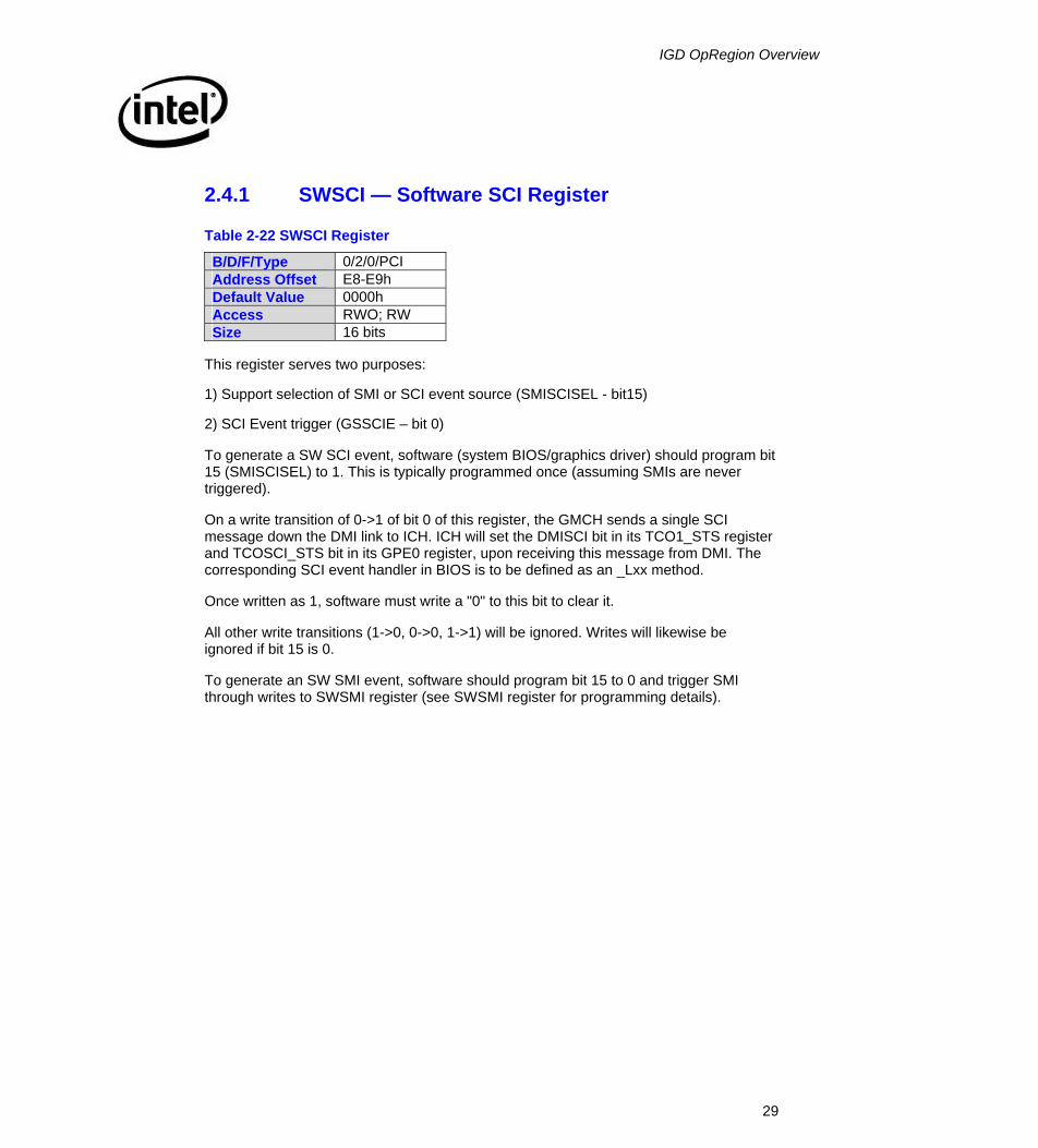
Table 2-22 SWSCI Register
B/D/F/Type 0/2/0/PCI Address Offset E8-E9h Default Value 0000h Access RWO; RW Size 16 bits
This register serves two purposes:
1) Support selection of SMI or SCI event source (SMISCISEL - bit15)
2) SCI Event trigger (GSSCIE – bit 0)
To generate a SW SCI event, software (system BIOS/graphics driver) should program bit 15 (SMISCISEL) to 1. This is typically programmed once (assuming SMIs are never triggered).
On a write transition of 0->1 of bit 0 of this register, the GMCH sends a single SCI message down the DMI link to ICH. ICH will set the DMISCI bit in its TCO1_STS register and TCOSCI_STS bit in its GPE0 register, upon receiving this message from DMI. The corresponding SCI event handler in BIOS is to be defined as an _Lxx method.
Once written as 1, software must write a "0" to this bit to clear it.
All other write transitions (1->0, 0->0, 1->1) will be ignored. Writes will likewise be ignored if bit 15 is 0.
To generate an SW SMI event, software should program bit 15 to 0 and trigger SMI through writes to SWSMI register (see SWSMI register for programming details).
IGD OpRegion Overview
30
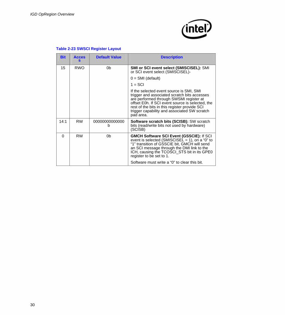
Table 2-23 SWSCI Register Layout
Bit Access
Default Value Description
15 RWO 0b SMI or SCI event select (SMISCISEL): SMI or SCI event select (SMISCISEL)- 0 = SMI (default) 1 = SCI If the selected event source is SMI, SMI trigger and associated scratch bits accesses are performed through SWSMI register at offset E0h. If SCI event source is selected, the rest of the bits in this register provide SCI trigger capability and associated SW scratch pad area.
14:1 RW 00000000000000b
Software scratch bits (SCISB): SW scratch bits (read/write bits not used by hardware) (SCISB)
0 RW 0b GMCH Software SCI Event (GSSCIE): If SCI event is selected (SMISCISEL = 1), on a “0” to “1” transition of GSSCIE bit, GMCH will send an SCI message through the DMI link to the ICH, causing the TCOSCI_STS bit in its GPE0 register to be set to 1. Software must write a “0” to clear this bit.

IGD OpRegion Mailboxes
31
3 IGD OpRegion Mailboxes This section contains descriptions of the mailboxes supported by the IGD OpRegion specification.
Note: The available mailboxes may vary from platform to platform, so make no assumptions about the availability of any given mailbox.
3.1 Mailbox #1: Public ACPI Methods Mailbox This mailbox supports ACPI events that result in Public ASL method execution, either in GFX scope or outside of GFX scope with graphics implications, such as docking/undocking events. A public method is one that’s documented in the ACPI specification.
All fields in this mailbox are either mandatory or optional. Optional fields are indicated as Diagnostic fields and are for debug or diagnostic purposes only. It is strongly recommended that optional fields are supported. Any invalid entry in the mandatory fields may result either unavailability of the feature or the graceful unloading of the graphics driver.
Table 3-1 Mailbox #1 - Public ACPI Methods: Table of Fields
Access Offset
(Bytes)
ASL Name
Size
(Bytes) SBIOS Driver
Description
0100h DRDY 0004h R* W** Driver Readiness 0104h
CSTS 0004h R/W R/W STATUS
0108h CEVT
0004h R/W R Current Event
010Ch RSV2 0014h N/A N/A Reserved
0120h DIDL
0020h R R/W Supported Display Devices ID List (_DOD)
0140h CPDL
0020h R R/W Currently Attached (or Present) Display Devices List
0160h CADL
0020h R R/W Currently Active Display Devices List (_DCS)
0180h
NADL 0020h
R/W
R/W
Next Active Devices List (_DGS use)
01A0h ASLP
0004h R W ASL Sleep Time Out
IGD OpRegion Mailboxes
32
Access Offset
(Bytes)
ASL Name
Size
(Bytes) SBIOS Driver
Description
01A4h
TIDX 0004h R/W R Toggle Table Index
01A8h CHPD
0004h R R/W Current Hotplug Enable Indicator
01Ach CLID
0004h R/W R Current Lid State Indicator
01B0h CDCK
0004h R/W R Current Docking State Indicator
01B4h SXSW
0004h R/W W Request ASL to issue Display Switch notification on Sx State resume
01B8h EVTS
0004h R/W R Events Supported by ASL (Diagnostic purpose only)
01BC CNOT
0004h R/W R/W Current OS Notification (Diagnostic purpose oly)
01C0 NRDY
0004h R R/W Driver Status (Diagnostic purpose only)
01C4h-01FFh
RSV3 0040h R/W R/W Reserved
* R = Read ** W = Write
Notes:
• The access level specified in this table for the SBIOS and driver is only a suggested guideline. Neither the graphics driver nor the operating system will enforce the guideline.
• Fields labeled ‘ Diagnostic Purposes Only’ are used for debugging purposes. Intel recommends that the OEMs/IBVs support these fields always. Unsupported diagnostic purposes fields do not, in any way, modify or change the behavior of the ACPI OpRegion’s published functionality.
• All entries in this header are DWORD aligned in regards to their physical addresses. This also means all addresses accessed by the system BIOS are DWORD aligned. The translated virtual address, provided to the graphics driver by the OS, can be set at any alignment.
The individual mailbox fields are detailed in the upcoming subsections.
IGD OpRegion Mailboxes
33
3.1.1 Driver Ready
Table 3-2 Driver Ready
Access Offset
(Bytes)
Size
(Bytes) SBIOS Driver
Contents
Fields, ASL Name (Recommended), Brief Text,
Values
0100h 0004h R W DWORD 0 – ‘DRDY’ Driver Readiness
Table 3-3 Driver Ready Details
Description This field indicates whether the graphics driver is ready to process ACPI video extension notifications from the system BIOS. The graphics driver may not be ready, for example, during initialization and resume. If the graphics driver is not ready, the driver may optionally indicate the reason why the graphics driver is not ready in the NRDY field. The authors of the graphics driver are strongly encouraged to provide a reason for not being ready.
The system BIOS ASL code has several options if the graphics driver is loaded but not ready:
• Fail the ACPI event processing gracefully without further graphics notifications. Where OS notifications are mandatory, they still need to be issued, such as Lid event.
• Sleep/Poll DRDY for driver readiness, timeout if the driver is not ready after a specified interval of time.
Note: If the graphics driver is not yet loaded, but the OSPM is ready, the system BIOS can fail ACPI video extensions gracefully.
Valid Values Bit Range[31:0]
Driver Readiness 0h - The driver not ready for video extensions calls 1h - The driver is ready for video extensions calls 2h-FFFFFFFFh – Reserved
System BIOS Access
This field is read by the system BIOS before: a) sending any notifications to the driver or b) handling ACPI video extensions.
Driver Access This field is set by the graphics driver after the successful loading, initialization and resume from sleep states (S3 & S4).
The graphics driver resets the field to 00h in cases of entering power management sleep states (S3 & S4). The graphics driver must also use this field to indicate the system BIOS in other cases where it is not ready to handle the ACPI video extension events. In
IGD OpRegion Mailboxes
34
all such cases, it is advisable that the driver set the information through NRDY, describing why the driver is not ready.
Relevant ACPI Methods
All ACPI video extensions methods. See ACPI specification ‘Video Extensions’ for details.
Relevant ACPI OS Notifications
All ACPI video extensions notifications. See ACPI specification ‘Video Extensions’ for details.
3.1.2 Notification Status
Table 3-4 Notification Status
Access Offset
(Bytes)
Size
(Bytes) SBIOS Driver
Contents
Fields, ASL Name (Recommended), Brief Text, Values
0104h 0004h R/W R/W DWORD 1 – ‘CSTS’ STATUS
Table 3-5 Notification Status Details
Description This field (Bit0 – Bit2) provides a graphics notification progress indicator. This serves as a handshake mechanism between the system BIOS ASL code and the graphics driver to process a specific graphics notification.
Valid Values Bit Range[31:0]
CSTS Field 0h – Success(Driver) 1h – Failure (Driver) 2h – Pending, Transaction (Driver) 3h – Dispatched, Transaction (ASL) 4h – FFFFFFFFh – Reserved
System BIOS Access
Writes: The system BIOS can only write a ‘Dispatched’ value to this field. This write should be done prior to any graphics notification issued by the system BIOS ASL code and only if the current status is success or failure.
Reads: The system BIOS can read this field anytime. The system BIOS sleeps or polls this field for a ‘success’ or ’failure’ status before issuing another notification or exiting the method.
Driver Access Writes: The graphics driver should initiate writes to this field only if the value is ‘dispatched’. Subsequent write values can be ‘pending’, followed by ‘success’ or ‘failure’. If the graphics driver writes ‘failure’, the driver may optionally indicate the reason of failure through the NRDY field. The authors of the graphics driver are strongly encouraged to provide a reason for the failure. Reads: The graphics driver can read this field any time. This field is typically read by the graphics driver on any graphics notification

IGD OpRegion Mailboxes
35
from the system BIOS ASL code or OSPM. The driver determines the origin of the driver call to be ASL if the value read back is ‘dispatched’. The driver would then acknowledge receipt of the notification by setting ‘Pending’ status before processing the notification. Upon completion, The driver would either set ‘success’ or ‘failure’. The driver shall not process the ASL notification if CSTS != Dispatched.
Relevant ACPI Methods
All ACPI video extensions methods. See ACPI specification ‘Video Extensions’ for details.
Relevant ACPI OS Notifications
All ACPI video extensions notifications. See ACPI specification ‘Video Extensions’ for details.
3.1.3 Current Event
Table 3-6 Current Event
Access
Offset
(Bytes)
Size
(Bytes)
SBIOS Driver
Contents
Fields, ASL Name (Recommended), Brief Text, Values
0108h 0004h R/W R DWORD 2 – ‘CEVT’ Current Event
Table 3-7 Current Event Details
Description This field indicates which current ACPI video extensions event trigger is being serviced. ASL sets this field to an appropriate value in response to a user activity of:
a. ACPI display switch key press b. Lid open/close c. Docking station (or port replicator) attach or detach
The intent of notifying the driver of the event is for the driver to apply appropriate persistence if necessary.
Display Switch Hotkey Press
Lid Open or Close
Dock or Undock
IGD OpRegion Mailboxes
36
Figure 3-1 CEVT – Current Event: Bit Field Definition
Valid Values Bit Range[31:0]
Event Description Value
No Event 0000h
Display Switch Hotkey Press Event 0001h
Lid Open or Close Event 0002h
Dock or Undock Event 0004h
Reserved 0008h - FFFFh
Table 3-8 CEVT - Current Event : Valid Values
Note: The bitwise flags in this field are exclusive. That is, only one bit should ever be set at any given time.
System BIOS Access
Writes: The system BIOS can write only one event value at a time.
Reads: The system BIOS can read this field any time, if required. The intent is for the system BIOS to serialize or block any potential back-to-back user event triggers.
Note: The system BIOS needs to update CEVT for Notify (VGA,0x80) only because this notification is overloaded for multiple ACPI events (hotkey, lid, dock) in XP.
Driver Access Writes: The graphics driver cannot write to this field.
Reads: The graphics driver typically reads this field in response to an OS call to switch displays or re-enumerate display devices so that it can apply appropriate persistence.
Relevant ACPI Methods
All ACPI video extensions methods. See ACPI specification ‘Video Extensions’ for details.
Relevant ACPI OS Notifications
Notify (VGA, 0x80) – Graphics display device switch

IGD OpRegion Mailboxes
37
3.1.4 Supported Display Devices ID List
Table 3-9 Supported Display Devices
Access Offset
(Bytes)
Size
(Bytes) SBIOS Driver
Contents
Fields, ASL Name (Recommended), Brief Text, Values
0120h 0020h R R/W DWORD 8-15 – ‘DIDL’ Supported Display Devices ID List (_DOD)
Table 3-10 Supported Display Devices Details
Description This field indicates which display devices are supported by the platform, and therefore enumerable by the graphics driver. A maximum of eight devices are assumed supportable on a given platform and enumerable by the graphics driver. The graphics driver detects or determines devices during its initialization and prior to the first monitor enumeration call it receives from the OS. The system BIOS uses this list (as is) to package a list of IDs and returns that list in _DOD method invocation. In the event of _DOD getting invoked by the OSPM prior to the graphics driver initializing this list, (that is, all IDs are 0), System BIOS _DOD method should return no enumerable connectors to the OSPM.
For description on _DOD ID formats, refer to “RS – ACPI _DOD ID’s for Intel® Integrated Graphics Software Interface Specification” document or “ACPI 3.0 Specification”.
The following table provides the layout of the ACPI ID list-based fields in this document, including CPDL, CADL, NADL, and DIDL.
If there are fewer than eight IDs, the graphics driver should terminate the list with 0 after the last ID.
Table 3-11 ACPI ID Layout
DWORD Offset
Description
0 ACPI ID 0 1 ACPI ID 1 2 ACPI ID 2 3 ACPI ID 3 4 ACPI ID 4 5 ACPI ID 5 6 ACPI ID 6 7 ACPI ID 7
IGD OpRegion Mailboxes
38
System BIOS Access
Writes: The system BIOS cannot write to these fields. Reads: The system BIOS can read this field anytime, if required. The intent is for the system BIOS to package this list without modification, when its _DOD method is invoked by OSPM.
Driver Access Writes: The graphics driver writes to this field once during its initialization, after determining the platform-supported connectors. Reads: The graphics driver can typically read this field as a sanity check during a monitor enumeration call from the OS.
Relevant ACPI Methods
_DOD
Relevant ACPI OS Notifications
Notify (VGA, 0) – Graphics device enumeration Notify (VGA, 0x81) – Some OS implementations cause serious side effects, so system BIOS implementations are advised to avoid this. Notify (\_SB.PCI0, 0) – PCI bus 0 wide enumeration
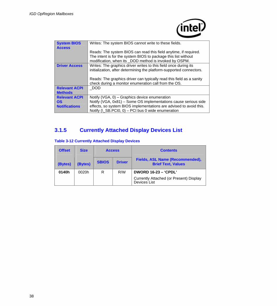
3.1.5 Currently Attached Display Devices List
Table 3-12 Currently Attached Display Devices
Access Offset
(Bytes)
Size
(Bytes) SBIOS Driver
Contents
Fields, ASL Name (Recommended), Brief Text, Values
0140h 0020h R R/W DWORD 16-23 – ‘CPDL’ Currently Attached (or Present) Display Devices List
IGD OpRegion Mailboxes
39
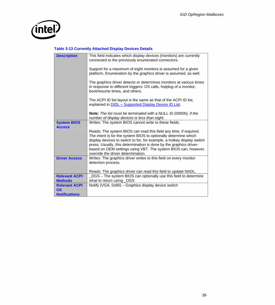
Table 3-13 Currently Attached Display Devices Details
Description This field indicates which display devices (monitors) are currently connected to the previously enumerated connectors. Support for a maximum of eight monitors is assumed for a given platform. Enumeration by the graphics driver is assumed, as well.
The graphics driver detects or determines monitors at various times in response to different triggers: OS calls, hotplug of a monitor, boot/resume times, and others.
The ACPI ID list layout is the same as that of the ACPI ID list, explained in DIDL – Supported Display Device ID List. Note: The list must be terminated with a NULL ID (0000h), if the number of display devices is less than eight.
System BIOS Access
Writes: The system BIOS cannot write to these fields.
Reads: The system BIOS can read this field any time, if required. The intent is for the system BIOS to optionally determine which display devices to switch to for, for example, a hotkey display switch press. Usually, this determination is done by the graphics driver-based on OEM settings using VBT. The system BIOS can, however, override the driver determination.
Driver Access Writes: The graphics driver writes to this field on every monitor detection process.
Reads: The graphics driver can read this field to update NADL.
Relevant ACPI Methods
_DGS – The system BIOS can optionally use this field to determine what to return using _DGS
Relevant ACPI OS Notifications
Notify (VGA, 0x80) – Graphics display device switch
IGD OpRegion Mailboxes
40
3.1.6 Currently Active Display Devices List
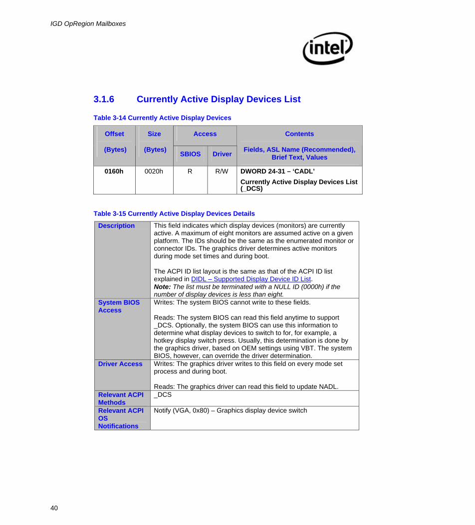
Table 3-14 Currently Active Display Devices
Access Offset
(Bytes)
Size
(Bytes) SBIOS Driver
Contents
Fields, ASL Name (Recommended), Brief Text, Values
0160h 0020h R R/W DWORD 24-31 – ‘CADL’ Currently Active Display Devices List (_DCS)
Table 3-15 Currently Active Display Devices Details
Description This field indicates which display devices (monitors) are currently active. A maximum of eight monitors are assumed active on a given platform. The IDs should be the same as the enumerated monitor or connector IDs. The graphics driver determines active monitors during mode set times and during boot.
The ACPI ID list layout is the same as that of the ACPI ID list explained in DIDL – Supported Display Device ID List. Note: The list must be terminated with a NULL ID (0000h) if the number of display devices is less than eight.
System BIOS Access
Writes: The system BIOS cannot write to these fields.
Reads: The system BIOS can read this field anytime to support _DCS. Optionally, the system BIOS can use this information to determine what display devices to switch to for, for example, a hotkey display switch press. Usually, this determination is done by the graphics driver, based on OEM settings using VBT. The system BIOS, however, can override the driver determination.
Driver Access Writes: The graphics driver writes to this field on every mode set process and during boot.
Reads: The graphics driver can read this field to update NADL.
Relevant ACPI Methods
_DCS
Relevant ACPI OS Notifications
Notify (VGA, 0x80) – Graphics display device switch

IGD OpRegion Mailboxes
41
3.1.7 Next Active Display Devices List
Table 3-16 Next Active Display Devices
Access Offset
(Bytes)
Size
(Bytes) SBIOS Driver
Contents
Fields, ASL Name (Recommended), Brief Text, Values
0180h 0020h R/W W DWORD 32-39 – ‘NADL’ Next Active Devices List (_DGS use)
Table 3-17 Next Active Display Devices Details
Description This field indicates which display the driver should switch to when a hotkey or lid event display switch event occurs. A maximum of eight monitors are assumed able to be switched to on a given platform. The IDs should be the same as the enumerated monitor or connector IDs. The graphics driver determines which monitors to switch to, based on selected toggle table (1 of 4) indicated by ‘TIDX’ by ASL code.
The graphics driver should update this field after a display change, hotplug, or unplug. ASL can override the driver selection if ASL maintains the toggle table internally, outside the VBT-based toggle tables.
The ACPI ID list layout is the same as that of the ACPI ID list, explained in DIDL – Supported Display Device ID List. Note: The list must be terminated with a NULL ID (0000h) if the number of display devices is less than eight.
System BIOS Access
Writes: The system BIOS should write to these fields to override the driver-determined next device list.
Reads: The system BIOS can read this field anytime to support _DGS. The system BIOS can either use this list as is to determine which display devices to switch to say for, for example, a hotkey display switch press or override it with its own.
Driver Access • Writes: The graphics driver writes to this field on every mode set process, any change in attached display devices, and during boot/resume.
• Reads: The graphics driver can read this field as a sanity check on display switch call from the OS.
Relevant ACPI Methods
_DGS
Relevant ACPI OS Notifications
Notify (VGA, 0x80) – Graphics display device switch
IGD OpRegion Mailboxes
42
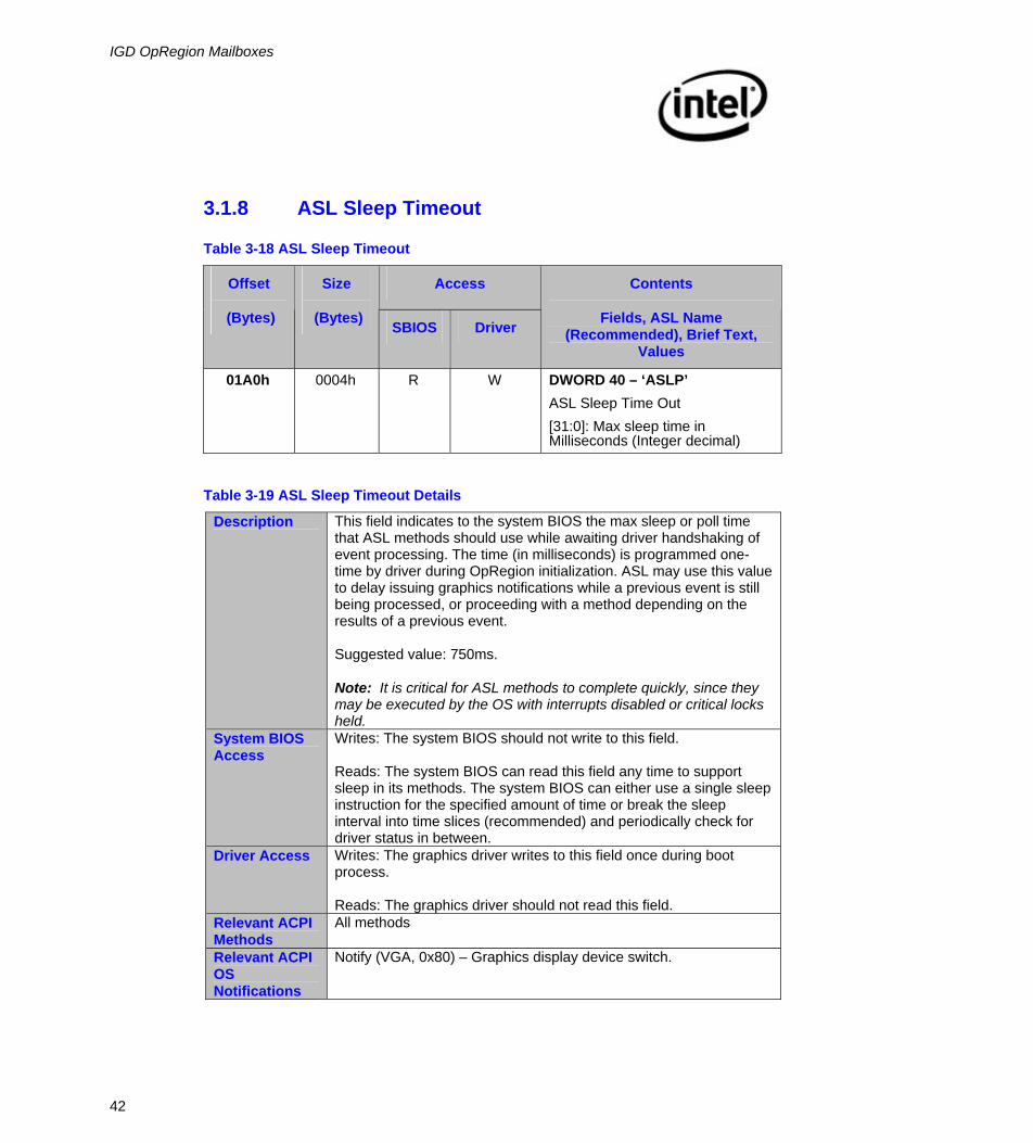
3.1.8 ASL Sleep Timeout
Table 3-18 ASL Sleep Timeout
Access Offset
(Bytes)
Size
(Bytes) SBIOS Driver
Contents
Fields, ASL Name (Recommended), Brief Text,
Values
01A0h 0004h R W DWORD 40 – ‘ASLP’ ASL Sleep Time Out [31:0]: Max sleep time in Milliseconds (Integer decimal)
Table 3-19 ASL Sleep Timeout Details
Description This field indicates to the system BIOS the max sleep or poll time that ASL methods should use while awaiting driver handshaking of event processing. The time (in milliseconds) is programmed one-time by driver during OpRegion initialization. ASL may use this value to delay issuing graphics notifications while a previous event is still being processed, or proceeding with a method depending on the results of a previous event.
Suggested value: 750ms. Note: It is critical for ASL methods to complete quickly, since they may be executed by the OS with interrupts disabled or critical locks held.
System BIOS Access
Writes: The system BIOS should not write to this field.
Reads: The system BIOS can read this field any time to support sleep in its methods. The system BIOS can either use a single sleep instruction for the specified amount of time or break the sleep interval into time slices (recommended) and periodically check for driver status in between.
Driver Access Writes: The graphics driver writes to this field once during boot process.
Reads: The graphics driver should not read this field.
Relevant ACPI Methods
All methods
Relevant ACPI OS Notifications
Notify (VGA, 0x80) – Graphics display device switch.
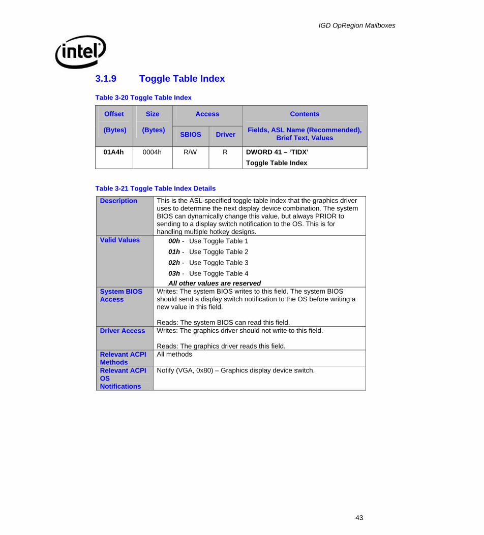
IGD OpRegion Mailboxes
43
3.1.9 Toggle Table Index
Table 3-20 Toggle Table Index
Access Offset
(Bytes)
Size
(Bytes) SBIOS Driver
Contents
Fields, ASL Name (Recommended), Brief Text, Values
01A4h
0004h R/W R DWORD 41 – ‘TIDX’ Toggle Table Index
Table 3-21 Toggle Table Index Details
Description This is the ASL-specified toggle table index that the graphics driver uses to determine the next display device combination. The system BIOS can dynamically change this value, but always PRIOR to sending to a display switch notification to the OS. This is for handling multiple hotkey designs.
Valid Values 00h - Use Toggle Table 1 01h - Use Toggle Table 2 02h - Use Toggle Table 3 03h - Use Toggle Table 4 All other values are reserved
System BIOS Access
Writes: The system BIOS writes to this field. The system BIOS should send a display switch notification to the OS before writing a new value in this field.
Reads: The system BIOS can read this field.
Driver Access Writes: The graphics driver should not write to this field.
Reads: The graphics driver reads this field. Relevant ACPI Methods
All methods
Relevant ACPI OS Notifications
Notify (VGA, 0x80) – Graphics display device switch.
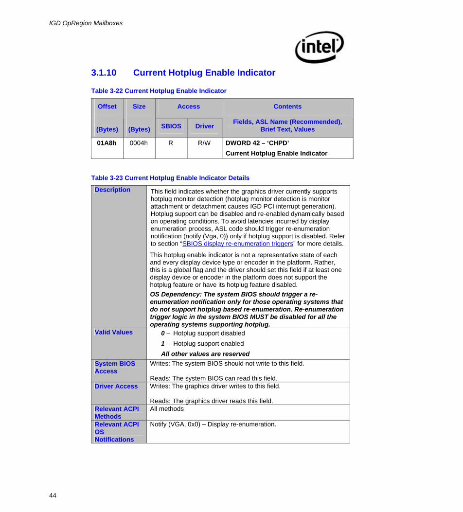
IGD OpRegion Mailboxes
44
3.1.10 Current Hotplug Enable Indicator
Table 3-22 Current Hotplug Enable Indicator
Access Offset
(Bytes)
Size
(Bytes) SBIOS Driver
Contents
Fields, ASL Name (Recommended), Brief Text, Values
01A8h 0004h R R/W DWORD 42 – ‘CHPD’ Current Hotplug Enable Indicator
Table 3-23 Current Hotplug Enable Indicator Details
Description This field indicates whether the graphics driver currently supports hotplug monitor detection (hotplug monitor detection is monitor attachment or detachment causes IGD PCI interrupt generation). Hotplug support can be disabled and re-enabled dynamically based on operating conditions. To avoid latencies incurred by display enumeration process, ASL code should trigger re-enumeration notification (notify (Vga, 0)) only if hotplug support is disabled. Refer to section “SBIOS display re-enumeration triggers” for more details.
This hotplug enable indicator is not a representative state of each and every display device type or encoder in the platform. Rather, this is a global flag and the driver should set this field if at least one display device or encoder in the platform does not support the hotplug feature or have its hotplug feature disabled. OS Dependency: The system BIOS should trigger a re-enumeration notification only for those operating systems that do not support hotplug based re-enumeration. Re-enumeration trigger logic in the system BIOS MUST be disabled for all the operating systems supporting hotplug.
Valid Values 0 – Hotplug support disabled 1 – Hotplug support enabled All other values are reserved
System BIOS Access
Writes: The system BIOS should not write to this field.
Reads: The system BIOS can read this field. Driver Access Writes: The graphics driver writes to this field.
Reads: The graphics driver reads this field.
Relevant ACPI Methods
All methods
Relevant ACPI OS Notifications
Notify (VGA, 0x0) – Display re-enumeration.
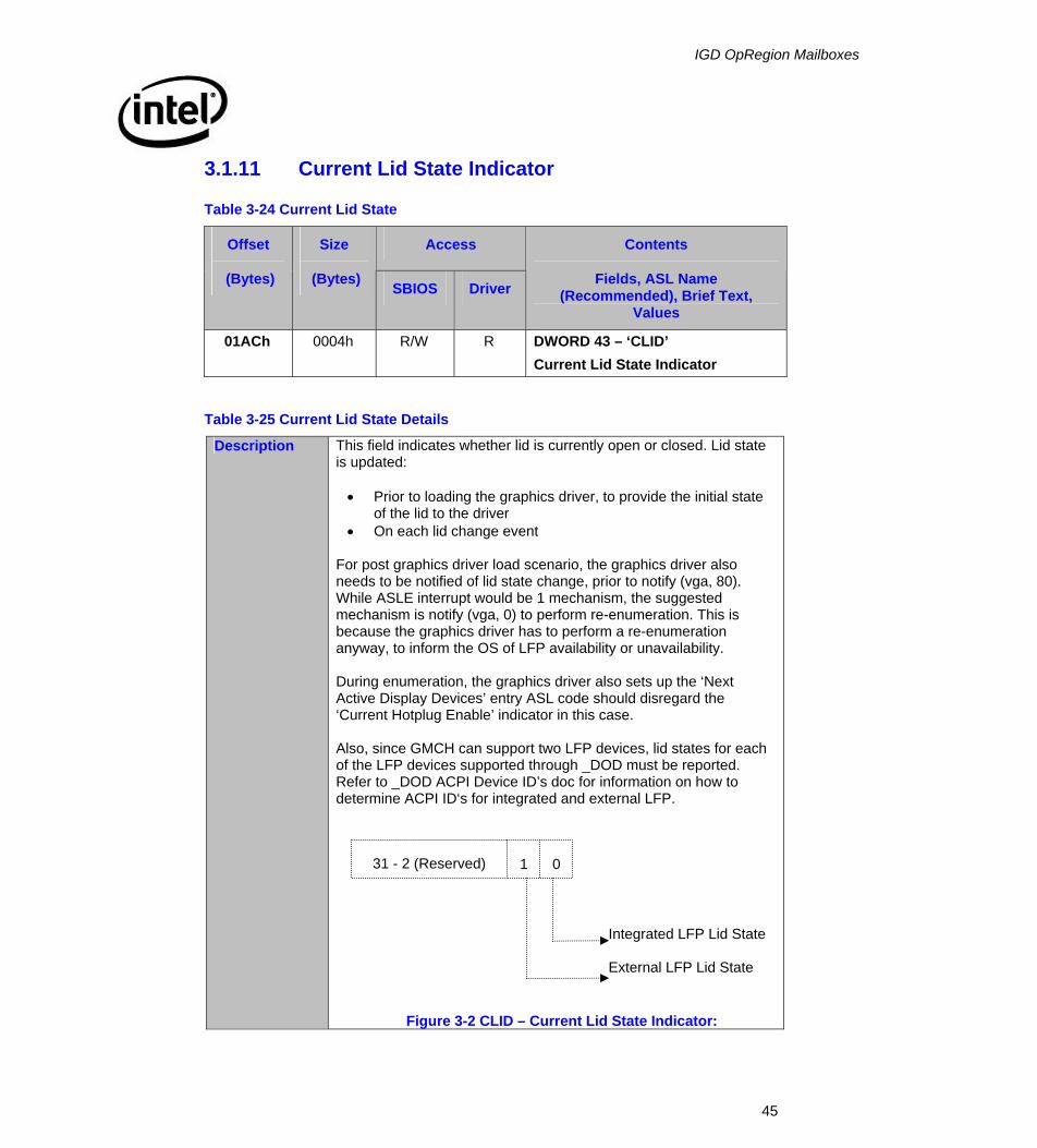
IGD OpRegion Mailboxes
45
3.1.11 Current Lid State Indicator
Table 3-24 Current Lid State
Access Offset
(Bytes)
Size
(Bytes) SBIOS Driver
Contents
Fields, ASL Name (Recommended), Brief Text,
Values
01ACh 0004h R/W R DWORD 43 – ‘CLID’ Current Lid State Indicator
Table 3-25 Current Lid State Details
Description This field indicates whether lid is currently open or closed. Lid state is updated:
• Prior to loading the graphics driver, to provide the initial state
of the lid to the driver • On each lid change event
For post graphics driver load scenario, the graphics driver also needs to be notified of lid state change, prior to notify (vga, 80). While ASLE interrupt would be 1 mechanism, the suggested mechanism is notify (vga, 0) to perform re-enumeration. This is because the graphics driver has to perform a re-enumeration anyway, to inform the OS of LFP availability or unavailability.
During enumeration, the graphics driver also sets up the ‘Next Active Display Devices’ entry ASL code should disregard the ‘Current Hotplug Enable’ indicator in this case.
Also, since GMCH can support two LFP devices, lid states for each of the LFP devices supported through _DOD must be reported. Refer to _DOD ACPI Device ID’s doc for information on how to determine ACPI ID‘s for integrated and external LFP.
Integrated LFP Lid State
External LFP Lid State
Figure 3-2 CLID – Current Lid State Indicator:
0 1 31 - 2 (Reserved)

IGD OpRegion Mailboxes
46
Bit Field Definition
Per Bit Field Interpretation
0 – LFP is closed 1 – LFP is open
Valid Values Table 3-26 CLID – Table of Valid Values
Description Value
All LFP lids are closed 0000h
Only internal LFP open 0001h
Only external LFP open 0002h
Both internal & external LFPs are open 0003h
Reserved 0004h - FFFFh
System BIOS Access
Writes: The system BIOS updates this field on lid events.
Reads: The system BIOS can read this field Driver Access Writes: The graphics driver should not write to this field.
Reads: The graphics driver reads this field.
Relevant ACPI Methods
All methods
Relevant ACPI OS Notifications
Notify (VGA, 0x80) - Graphics display switch Notify (VGA, 0x0) - Display re-enumeration
3.1.12 Current Docking State Indicator
Table 3-27 Current Docking State
Access Offset
(Bytes)
Size
(Bytes) SBIOS Driver
Contents
Fields, ASL Name (Recommended), Brief Text, Values
01B0h 0004h R/W R DWORD 43 – ‘CDCK’ Current Docking State Indicator
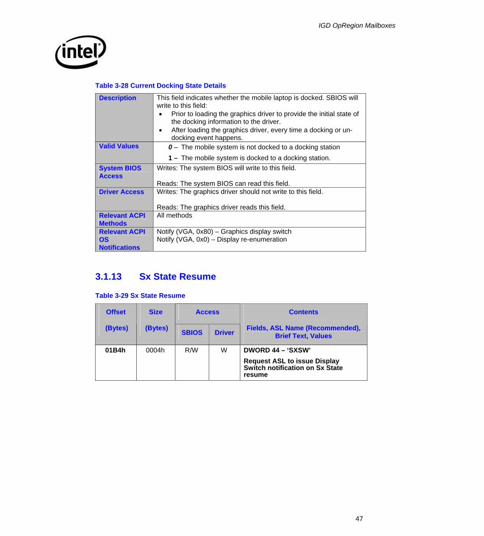
IGD OpRegion Mailboxes
47
Table 3-28 Current Docking State Details
Description This field indicates whether the mobile laptop is docked. SBIOS will write to this field: • Prior to loading the graphics driver to provide the initial state of
the docking information to the driver. • After loading the graphics driver, every time a docking or un-
docking event happens. Valid Values 0 – The mobile system is not docked to a docking station
1 – The mobile system is docked to a docking station. System BIOS Access
Writes: The system BIOS will write to this field.
Reads: The system BIOS can read this field. Driver Access Writes: The graphics driver should not write to this field.
Reads: The graphics driver reads this field.
Relevant ACPI Methods
All methods
Relevant ACPI OS Notifications
Notify (VGA, 0x80) – Graphics display switch Notify (VGA, 0x0) – Display re-enumeration
3.1.13 Sx State Resume
Table 3-29 Sx State Resume
Access Offset
(Bytes)
Size
(Bytes) SBIOS Driver
Contents
Fields, ASL Name (Recommended), Brief Text, Values
01B4h 0004h R/W W DWORD 44 – ‘SXSW’ Request ASL to issue Display Switch notification on Sx State resume
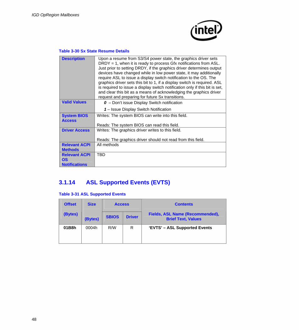
IGD OpRegion Mailboxes
48
Table 3-30 Sx State Resume Details
Description Upon a resume from S3/S4 power state, the graphics driver sets DRDY = 1, when it is ready to process Gfx notifications from ASL. Just prior to setting DRDY, if the graphics driver determines output devices have changed while in low power state, it may additionally require ASL to issue a display switch notification to the OS. The graphics driver sets this bit to 1, if a display switch is required. ASL is required to issue a display switch notification only if this bit is set, and clear this bit as a means of acknowledging the graphics driver request and preparing for future Sx transitions.
Valid Values 0 – Don’t issue Display Switch notification 1 – Issue Display Switch Notification
System BIOS Access
Writes: The system BIOS can write into this field.
Reads: The system BIOS can read this field. Driver Access Writes: The graphics driver writes to this field.
Reads: The graphics driver should not read from this field.
Relevant ACPI Methods
All methods
Relevant ACPI OS Notifications
TBD
3.1.14 ASL Supported Events (EVTS)
Table 3-31 ASL Supported Events
Access Offset
(Bytes)
Size
(Bytes) SBIOS Driver
Contents
Fields, ASL Name (Recommended), Brief Text, Values
01B8h 0004h R/W R ‘EVTS’ – ASL Supported Events

IGD OpRegion Mailboxes
49
Table 3-32 ASL Supported Events Details
Description It indicates the events supported in ASL code. This field is for driver information (diagnostic purposes) only.
Valid Values Bit Range[31:0] Table 3-33 EVTS – ASL Supported Events: Valid Values
Bit Range[31:0]
Details
Bit[31:3] Reserved Bit[2] Dock/Undock
This bit contains information on if Dock/Undock event bit is supported or not.
0 = Event not supported 1 = Event supported
Bit[1] Lid Open/Close This bit contains information on if Lid
Open/Close event bit is supported or not. 0 = Event not supported 1 = Event supported
Bit[0] Display switch Hotkey press This bit contains information on if Display
switch hotkey press event bit is supported or not.
0 = Event not supported 1 = Event supported
System BIOS Access
Writes: The system BIOS POST or ASL code can write to this field. Reads: The system BIOS POST or ASL code can read this field.
Driver Access Writes: The graphics driver should not write to this field.
Reads: The graphics driver reads from this field. Relevant ACPI Methods
All methods
Relevant ACPI OS Notifications
None

IGD OpRegion Mailboxes
50
3.1.15 Current OS Notification (CNOT)
Table 3-34 Current OS Notification
Access Offset
(Bytes)
Size
(Bytes) SBIOS Driver
Contents
Fields, ASL Name (Recommended), Brief Text,
Values
01BCh 0004h R/W R/W ‘CNOT’ – Current OS Notification
Table 3-35 Current OS Notification Details
Description It indicates what OS notification is about to be issued to service the current event.
Valid Values Bit Range[31:0]
Table 3-36: CNOT - Current OS Notification: Value Values
Bit Range[31:0]
Details
Bit[31:5] Reserved Bit[4] Undocked State
This bit contains information on if the Undocked State is about to be issued by OS to service the current event
0 = No Service 1 = Currently servicing this event
Bit[3] Docked State This bit contains information on if the
Docked State is about to be issued by OS to service the current event
0 = No Service 1 = Currently servicing this event
Bit[2] Lid State This bit contains information on if the Lid
State is about to be issued by OS to service the current event
0 = No Service 1 = Currently servicing this event
Bit[1] Re-enumerate This bit contains information on if the Re-
enumerate State is about to be issued by OS to service the current event
0 = No Service 1 = Currently servicing this event
Bit[0] Display Switch This bit contains information on if the

IGD OpRegion Mailboxes
51
Undocked State is about to be issued by OS to service the current event
0 = No Service 1 = Currently servicing this event
Note: Only one bit can be selected at a time. System BIOS Access
Writes: The system BIOS POST or ASL code can write to this field. Reads: The system BIOS POST or ASL code can read this field.
Driver Access Writes: The graphics driver should write to this field.
Reads: The graphics driver reads from this field. Relevant ACPI Methods
All methods
Relevant ACPI OS Notifications
None
3.1.16 Driver Status (NRDY)
Table 3-37 Driver Status
Access Offset
(Bytes)
Size
(Bytes) SBIOS Driver
Contents
Fields, ASL Name (Recommended), Brief Text, Values
01C0h 0004h R R/W ‘NRDY’ – Driver Status
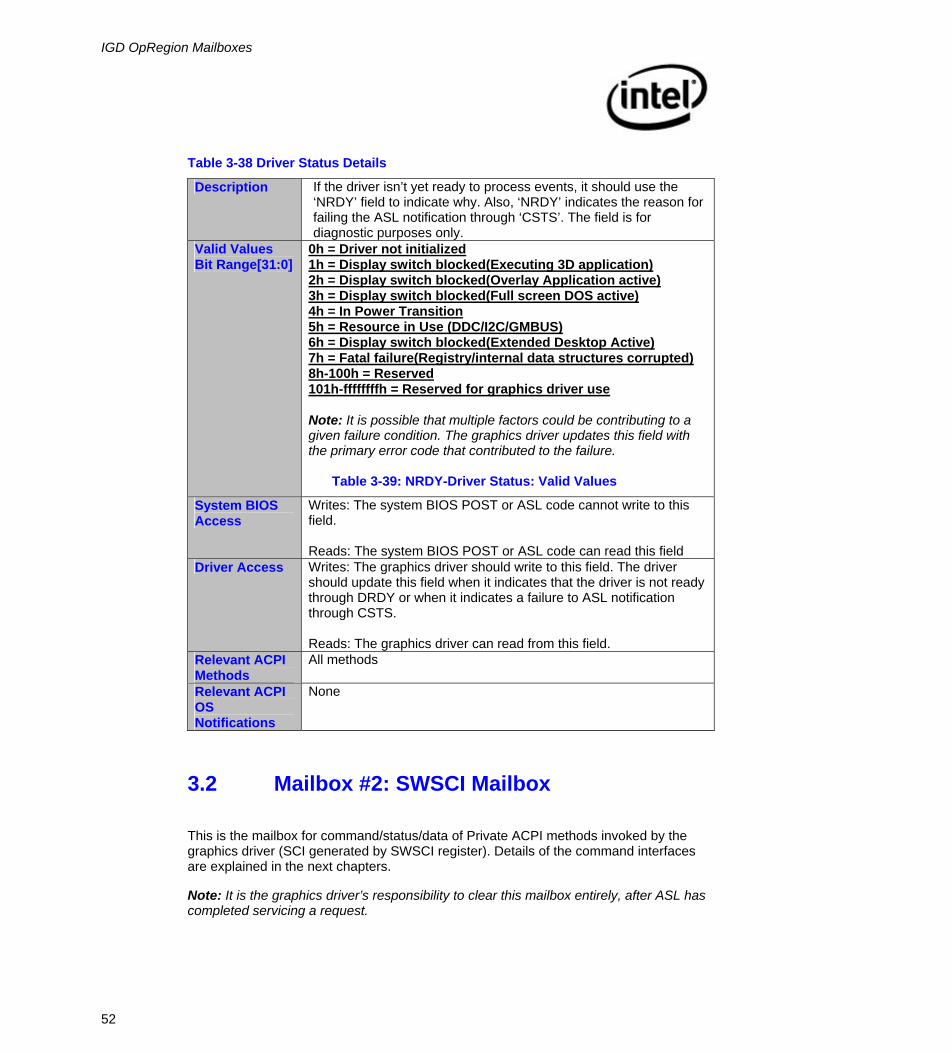
IGD OpRegion Mailboxes
52
Table 3-38 Driver Status Details
Description If the driver isn’t yet ready to process events, it should use the ‘NRDY’ field to indicate why. Also, ‘NRDY’ indicates the reason for failing the ASL notification through ‘CSTS’. The field is for diagnostic purposes only.
Valid Values Bit Range[31:0]
0h = Driver not initialized 1h = Display switch blocked(Executing 3D application) 2h = Display switch blocked(Overlay Application active) 3h = Display switch blocked(Full screen DOS active) 4h = In Power Transition 5h = Resource in Use (DDC/I2C/GMBUS) 6h = Display switch blocked(Extended Desktop Active) 7h = Fatal failure(Registry/internal data structures corrupted) 8h-100h = Reserved 101h-ffffffffh = Reserved for graphics driver use Note: It is possible that multiple factors could be contributing to a given failure condition. The graphics driver updates this field with the primary error code that contributed to the failure.
Table 3-39: NRDY-Driver Status: Valid Values
System BIOS Access
Writes: The system BIOS POST or ASL code cannot write to this field. Reads: The system BIOS POST or ASL code can read this field
Driver Access Writes: The graphics driver should write to this field. The driver should update this field when it indicates that the driver is not ready through DRDY or when it indicates a failure to ASL notification through CSTS.
Reads: The graphics driver can read from this field.
Relevant ACPI Methods
All methods
Relevant ACPI OS Notifications
None
3.2 Mailbox #2: SWSCI Mailbox
This is the mailbox for command/status/data of Private ACPI methods invoked by the graphics driver (SCI generated by SWSCI register). Details of the command interfaces are explained in the next chapters.
Note: It is the graphics driver’s responsibility to clear this mailbox entirely, after ASL has completed servicing a request.
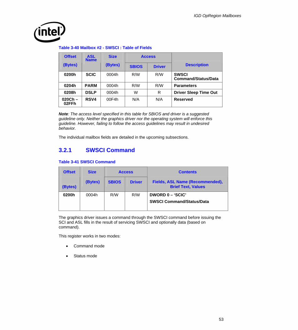
IGD OpRegion Mailboxes
53
Table 3-40 Mailbox #2 - SWSCI : Table of Fields
Access Offset
(Bytes)
ASL Name
Size
(Bytes) SBIOS Driver
Description
0200h SCIC 0004h R/W R/W SWSCI Command/Status/Data
0204h PARM 0004h R/W R/W Parameters 0208h DSLP 0004h W R Driver Sleep Time Out
020Ch –02FFh
RSV4 00F4h N/A N/A Reserved
Note: The access level specified in this table for SBIOS and driver is a suggested guideline only. Neither the graphics driver nor the operating system will enforce this guideline. However, failing to follow the access guidelines may result in undesired behavior.
The individual mailbox fields are detailed in the upcoming subsections.
3.2.1 SWSCI Command
Table 3-41 SWSCI Command
Access Offset
(Bytes)
Size
(Bytes) SBIOS Driver
Contents
Fields, ASL Name (Recommended), Brief Text, Values
0200h 0004h R/W R/W DWORD 0 – ‘SCIC’ SWSCI Command/Status/Data
The graphics driver issues a command through the SWSCI command before issuing the SCI and ASL fills in the result of servicing SWSCI and optionally data (based on command).
This register works in two modes:
• Command mode
• Status mode

IGD OpRegion Mailboxes
54
3.2.1.1 Command Mode
In this mode, the graphics driver sends command to the ASL code. The following bit definition is defined for the SCIC command mode.
SWSCI Command (Bit 0 = 1) – The graphics driver sets this bit before triggering the SWSCI through the PCI configuration register. This bit is checked by the ASL code for authentication purposes – to make sure that the caller is in fact the graphics driver. Reserved fields are set to 0.
3.2.1.2 Status Mode
In this mode, the ASL has executed the command requested by the graphics driver in the command mode and the status is given by the ASL. The following bit definition is defined for the SCIC status mode.
SWSCI Status (Bit 0 = 0) – ASL clears the bit 0 (SWSCI status) and then updates the appropriate result and exit codes, after completion of the service request is given in the command mode. Reserved fields are set to 0.
0 (Reseved)
4 – 1 Function
Code
7 – 5 (Reserved
)
31-16 (Reserved)
15 – 8 Sub-Function
Code
0 (Reserved)
4 – 1 (Reserved)
7 – 5 Result
31-16 (Reserved)
15 – 8 Exit Code

IGD OpRegion Mailboxes
55
3.2.2 SWSCI Parameters
Table 3-42 SWSCI Parameters
Access Offset
(Bytes)
Size
(Bytes) SBIOS Driver
Contents
Fields, ASL Name (Recommended), Brief Text, Values
0204h 0004h R/W R/W DWORD 1 – ‘PARM’ Parameters [31:0]: Parameter
This field is used by both the graphics driver and ASL code to pass on parameters that are used in command as well as in status mode of SCIC field.
3.2.3 SWSCI Driver Sleep Timeout
Table 3-43 SWSCI Driver Sleep Timeout
Access Offset
(Bytes)
Size
(Bytes) SBIOS Driver
Contents
Fields, ASL Name (Recommended), Brief Text,
Values
0204h 0004h W R DWORD 1 – ‘DSLP’ Driver Sleep Time Out [31:0]: Driver Sleep Time Out Value
This field is written once by the system BIOS, during initialization with a time out value of the SCI handler to respond back. The driver has to poll for the SCI’s response for the maximum time out period specified by this field. On timeout, the driver has to consider this a failure and return back the failure status.

IGD OpRegion Mailboxes
56
3.3 Mailbox #3: ASLE Support This is the mailbox for communicating all driver features related information between the driver and the SBIOS. Details of the commands interfaces are explained in the next chapters.
Table 3-44 Mailbox #3 - ASLE Support: Table of Fields
Access Offset
(Bytes)
ASL Name
Size
(Bytes) SBIOS Driver
Description
0300h ARDY 0004h R W Driver Readiness 0304h ASLC 0004h R/W R/W ASLE Interrupt
Command/Status 0308h TCHE 0004h R/W R/W Technology Enabled Indicator 030Ch ALSI 0004h W R Current ALS Luminance
Reading (in Lux) 0310h BCLP 0004h W R Requested Backlight
Brightness 0314h PFIT 0004h W R Panel Fitting State or Request 0318h CBLV 0004h R/W W Current Brightness Level 031Ch BCLM 0028h W R Backlight Brightness Levels
Duty Cycle Mapping Table 0344h CPFM 0004h W R Current Panel Fitting Mode 0348h EPFM 0004h W R Enabled Panel Fitting Modes 034Ch PLUT 004Ah W R Panel LUT & Identifier 0396h PFMB 0004h W R PWM Frequency and Minimum
Brightness 0400h CCDV 0004h W R Color Correction Default
Values
Notes:
• The access level specified in this table for the SBIOS and driver is a suggested guideline only. Neither the graphics driver nor the operating system will enforce the guideline.
• Fields labeled ‘Diagnostic Purposes Only’ are used for debugging purposes. Intel recommends the OEMs/IBVs to support these fields always. Unsupported diagnostic purposes fields do not, in any way, modify or change the behavior of the ACPI OpRegion’s published functionality.
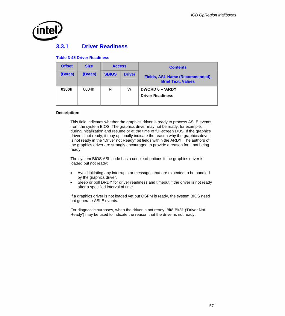
IGD OpRegion Mailboxes
57
3.3.1 Driver Readiness
Table 3-45 Driver Readiness
Access Offset
(Bytes)
Size
(Bytes) SBIOS Driver Contents
Fields, ASL Name (Recommended), Brief Text, Values
0300h 0004h R W DWORD 0 – ‘ARDY’ Driver Readiness
Description:
This field indicates whether the graphics driver is ready to process ASLE events from the system BIOS. The graphics driver may not be ready, for example, during initialization and resume or at the time of full-screen DOS. If the graphics driver is not ready, it may optionally indicate the reason why the graphics driver is not ready in the “Driver not Ready” bit fields within the ARDY. The authors of the graphics driver are strongly encouraged to provide a reason for it not being ready. The system BIOS ASL code has a couple of options if the graphics driver is loaded but not ready: • Avoid initiating any interrupts or messages that are expected to be handled
by the graphics driver. • Sleep or poll DRDY for driver readiness and timeout if the driver is not ready
after a specified interval of time
If a graphics driver is not loaded yet but OSPM is ready, the system BIOS need not generate ASLE events. For diagnostic purposes, when the driver is not ready, Bit8-Bit31 (‘Driver Not Ready’) may be used to indicate the reason that the driver is not ready.
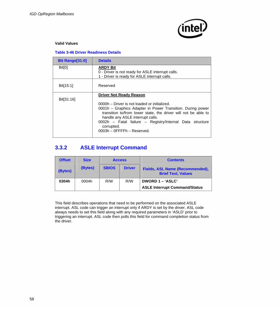
IGD OpRegion Mailboxes
58
Valid Values
Table 3-46 Driver Readiness Details
Bit Range[31:0] Details Bit[0] ARDY Bit
0 - Driver is not ready for ASLE interrupt calls. 1 - Driver is ready for ASLE interrupt calls.
Bit[15:1]
Reserved
Bit[31:16]
Driver Not Ready Reason 0000h – Driver is not loaded or initialized. 0001h – Graphics Adapter in Power Transition. During power
transition to/from lower state, the driver will not be able to handle any ASLE interrupt calls.
0002h – Fatal failure – Registry/Internal Data structure corrupted.
0003h – 0FFFFh – Reserved.
3.3.2 ASLE Interrupt Command
Access Offset
(Bytes)
Size
(Bytes) SBIOS Driver
Contents
Fields, ASL Name (Recommended), Brief Text, Values
0304h 0004h R/W R/W DWORD 1 – ‘ASLC’ ASLE Interrupt Command/Status
This field describes operations that need to be performed on the associated ASLE interrupt. ASL code can trigger an interrupt only if ARDY is set by the driver. ASL code always needs to set this field along with any required parameters in ‘ASLD’ prior to triggering an interrupt. ASL code then polls this field for command completion status from the driver.
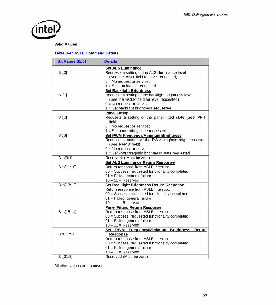
IGD OpRegion Mailboxes
59
Valid Values
Table 3-47 ASLE Command Details
Bit Range[31:0] Details Bit[0]
Set ALS Luminance Requests a setting of the ALS illuminance level
(See the ‘ASLI’ field for level requested) 0 = No request or serviced 1 = Set Luminance requested
Bit[1]
Set Backlight Brightness Requests a setting of the backlight brightness level
(See the ‘BCLP’ field for level requested) 0 = No request or serviced 1 = Set backlight brightness requested
Bit[2]
Panel Fitting Requests a setting of the panel fitted state (See ‘PFIT’
field) 0 = No request or serviced 1 = Set panel fitting state requested
Bit[3] Set PWM Frequency/Minimum Brightness Requests a setting of the PWM freq/min brightness state
(See ‘PFMB’ field) 0 = No request or serviced 1 = Set PWM freq/min brightness state requested
Bits[9:4] Reserved. ( Must be zero) Bits[11:10]
Set ALS Luminance Return Response Return response from ASLE interrupt. 00 = Success, requested functionality completed 01 = Failed, general failure 10 – 11 = Reserved
Bits[13:12] Set Backlight Brightness Return Response Return response from ASLE interrupt. 00 = Success, requested functionality completed 01 = Failed, general failure 10 – 11 = Reserved
Bits[15:14]
Panel Fitting Return Response Return response from ASLE interrupt. 00 = Success, requested functionality completed 01 = Failed, general failure 10 – 11 = Reserved
Bits[17:16]
Set PWM Frequency/Minimum Brightness Return Response
Return response from ASLE interrupt. 00 = Success, requested functionality completed 01 = Failed, general failure 10 – 11 = Reserved
Bit[31:8] Reserved (Must be zero) All other values are reserved.
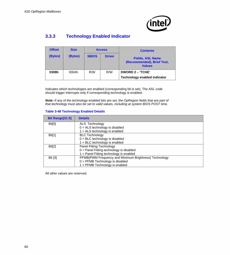
IGD OpRegion Mailboxes
60
3.3.3 Technology Enabled Indicator
Access Offset
(Bytes)
Size
(Bytes) SBIOS Driver Contents
Fields, ASL Name (Recommended), Brief Text,
Values
0308h 0004h R/W R/W DWORD 2 – ‘TCHE’ Technology enabled indicator
Indicates which technologies are enabled (corresponding bit is set). The ASL code should trigger interrupts only if corresponding technology is enabled.
Note: If any of the technology enabled bits are set, the OpRegion fields that are part of that technology must also be set to valid values, including at system BIOS POST time.
Table 3-48 Technology Enabled Details
Bit Range[31:0] Details Bit[0] ALS Technology
0 = ALS technology is disabled 1 = ALS technology is enabled
Bit[1] BLC Technology 0 = BLC technology is disabled 1 = BLC technology is enabled
Bit[2] Panel Fitting Technology 0 = Panel Fitting technology is disabled 1 = Panel Fitting technology is enabled
Bit [3] PFMB(PWM Frequency and Minimum Brightness) Technology 0 = PFMB Technology is disabled 1 = PFMB Technology is enabled
All other values are reserved.

IGD OpRegion Mailboxes
61
3.3.4 Current ALS Luminance Reading
The ‘ALSI’ field contains the current ALS luminance reading.
Note: This field shall be set prior to the ASLE interrupt requesting a luminance change.
Access Offset
(Bytes)
Size
(Bytes) SBIOS Driver Contents
Fields, ASL Name (Recommended), Brief Text, Values
030Ch 0004h W R DWORD 3 – ‘ALSI’ Current ALS Illuminance reading (in lux)
Valid Values
Table 3-49 ALS Luminance Details
Bit Range[31:0] Details Bit[31-0]
0000h – Current reading below sensor range FFFFh – Current reading above sensor range 1 ~ FFFEh – Current Illuminance reading
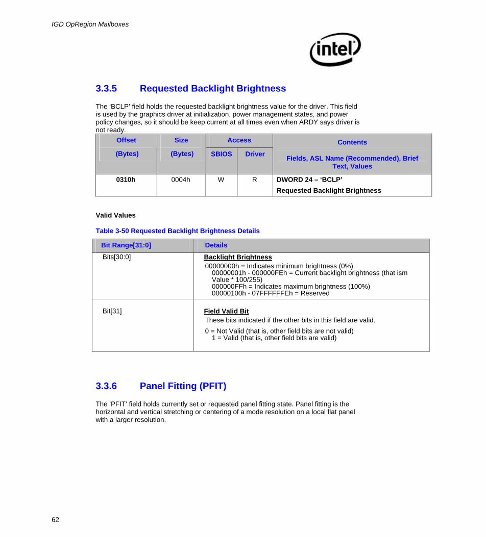
IGD OpRegion Mailboxes
62
3.3.5 Requested Backlight Brightness
The ‘BCLP’ field holds the requested backlight brightness value for the driver. This field is used by the graphics driver at initialization, power management states, and power policy changes, so it should be keep current at all times even when ARDY says driver is not ready.
Access Offset
(Bytes)
Size
(Bytes) SBIOS Driver Contents
Fields, ASL Name (Recommended), Brief Text, Values
0310h 0004h W R DWORD 24 – ‘BCLP’ Requested Backlight Brightness
Valid Values
Table 3-50 Requested Backlight Brightness Details
Bit Range[31:0] Details Bits[30:0] Backlight Brightness
00000000h = Indicates minimum brightness (0%) 00000001h - 000000FEh = Current backlight brightness (that ism Value * 100/255) 000000FFh = Indicates maximum brightness (100%) 00000100h - 07FFFFFFEh = Reserved
Bit[31]
Field Valid Bit These bits indicated if the other bits in this field are valid. 0 = Not Valid (that is, other field bits are not valid)
1 = Valid (that is, other field bits are valid)
3.3.6 Panel Fitting (PFIT)
The ‘PFIT’ field holds currently set or requested panel fitting state. Panel fitting is the horizontal and vertical stretching or centering of a mode resolution on a local flat panel with a larger resolution.

IGD OpRegion Mailboxes
63
Table 3-51 Panel fitting
Access Offset
(Bytes)
Size
(Bytes) SBIOS Driver Contents
Fields, ASL Name (Recommended), Brief Text, Values
0314h 0004h W R Panel Fitting current state or request
Valid Values
Table 3-52 Panel Fitting Details
Bit Range[31:0] Details
Bit [0] Centering Centers a smaller mode resolution within a larger local flat panel resolution. 0 = Centering not requested
1 = Center Mode on Panel
Bit [1] Text Mode stretching Stretch text modes whenever they are set and can be stretched. 0 = Do not stretch text modes
1 = Stretch text modes
Bit[2] Graphics Mode stretching Stretch graphics modes whenever they are set and can be stretched. 0 = Do not stretch graphics modes
1 = Stretch graphics modes
Bits[30:3] Reserved (Must be zero)
Bit[31] Field Valid Bit These bits indicated if the other bits in this field are valid. 0 = Not Valid (that is, other field bits are not valid)
1 = Valid (that is, other field bits are valid)
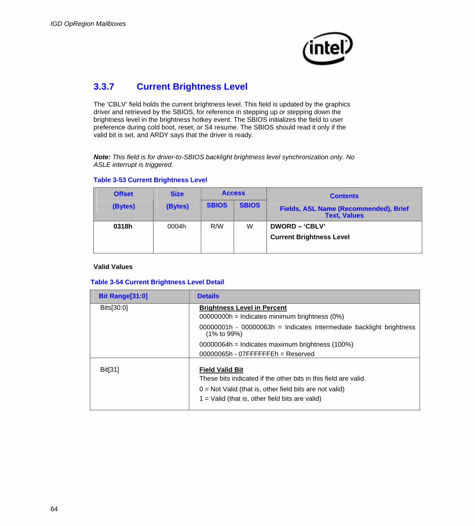
IGD OpRegion Mailboxes
64
3.3.7 Current Brightness Level
The ‘CBLV’ field holds the current brightness level. This field is updated by the graphics driver and retrieved by the SBIOS, for reference in stepping up or stepping down the brightness level in the brightness hotkey event. The SBIOS initializes the field to user preference during cold boot, reset, or S4 resume. The SBIOS should read it only if the valid bit is set, and ARDY says that the driver is ready.
Note: This field is for driver-to-SBIOS backlight brightness level synchronization only. No ASLE interrupt is triggered.
Table 3-53 Current Brightness Level
Access Offset
(Bytes)
Size
(Bytes) SBIOS SBIOS Contents
Fields, ASL Name (Recommended), Brief Text, Values
0318h 0004h R/W W DWORD – ‘CBLV’ Current Brightness Level
Valid Values
Table 3-54 Current Brightness Level Detail
Bit Range[31:0] Details Bits[30:0] Brightness Level in Percent
00000000h = Indicates minimum brightness (0%) 00000001h - 00000063h = Indicates Intermediate backlight brightness
(1% to 99%) 00000064h = Indicates maximum brightness (100%) 00000065h - 07FFFFFFEh = Reserved
Bit[31]
Field Valid Bit These bits indicated if the other bits in this field are valid. 0 = Not Valid (that is, other field bits are not valid) 1 = Valid (that is, other field bits are valid)
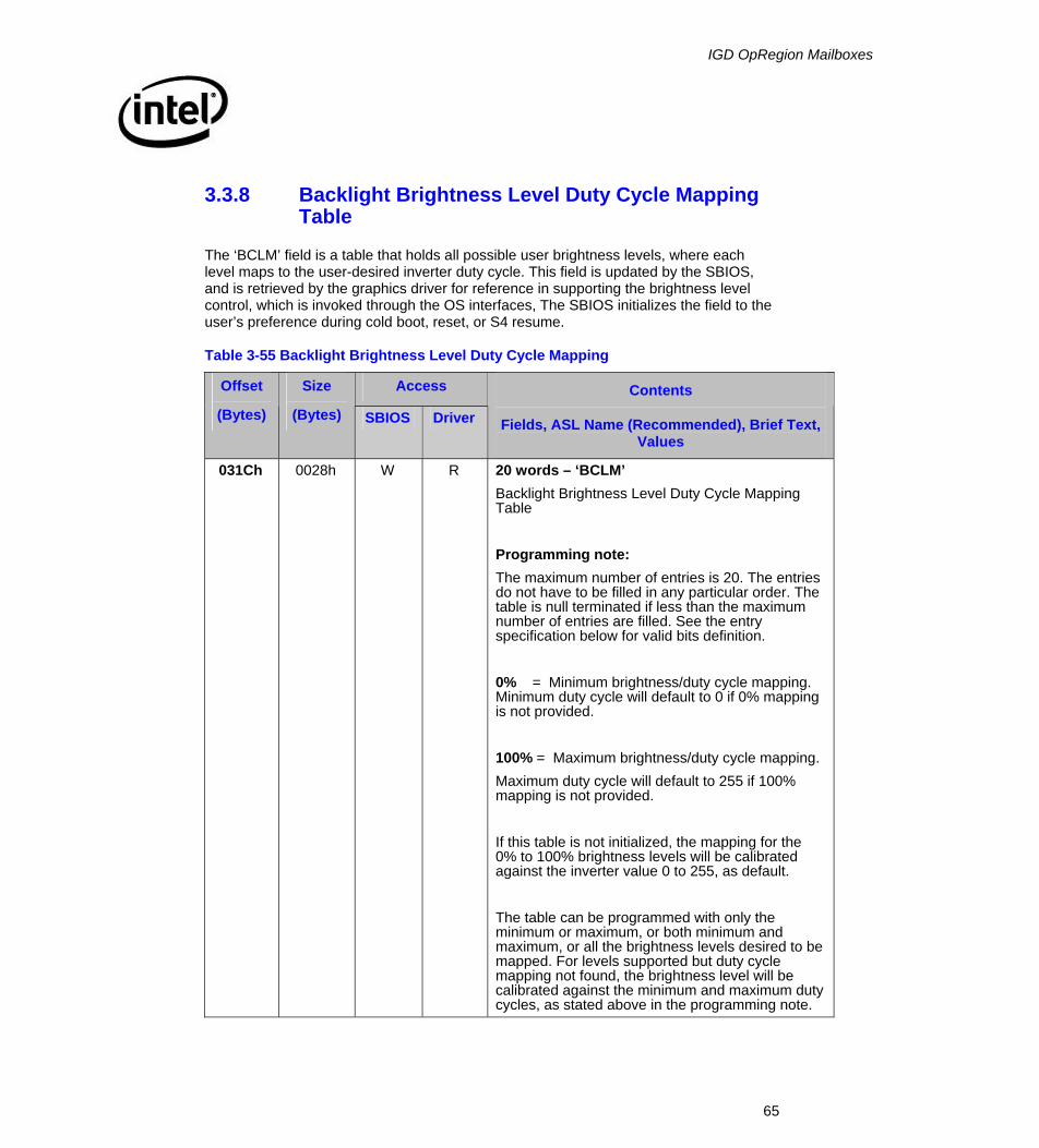
IGD OpRegion Mailboxes
65
3.3.8 Backlight Brightness Level Duty Cycle Mapping Table
The ‘BCLM’ field is a table that holds all possible user brightness levels, where each level maps to the user-desired inverter duty cycle. This field is updated by the SBIOS, and is retrieved by the graphics driver for reference in supporting the brightness level control, which is invoked through the OS interfaces, The SBIOS initializes the field to the user’s preference during cold boot, reset, or S4 resume.
Table 3-55 Backlight Brightness Level Duty Cycle Mapping
Access Offset
(Bytes)
Size
(Bytes) SBIOS Driver
Contents
Fields, ASL Name (Recommended), Brief Text, Values
031Ch 0028h W R 20 words – ‘BCLM’ Backlight Brightness Level Duty Cycle Mapping Table Programming note: The maximum number of entries is 20. The entries do not have to be filled in any particular order. The table is null terminated if less than the maximum number of entries are filled. See the entry specification below for valid bits definition. 0% = Minimum brightness/duty cycle mapping. Minimum duty cycle will default to 0 if 0% mapping is not provided. 100% = Maximum brightness/duty cycle mapping. Maximum duty cycle will default to 255 if 100% mapping is not provided. If this table is not initialized, the mapping for the 0% to 100% brightness levels will be calibrated against the inverter value 0 to 255, as default. The table can be programmed with only the minimum or maximum, or both minimum and maximum, or all the brightness levels desired to be mapped. For levels supported but duty cycle mapping not found, the brightness level will be calibrated against the minimum and maximum duty cycles, as stated above in the programming note.
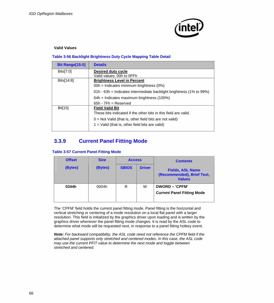
IGD OpRegion Mailboxes
66
Valid Values
Table 3-56 Backlight Brightness Duty Cycle Mapping Table Detail
Bit Range[15:0] Details Bits[7:0] Desired duty cycle
Valid values: 00h to 0FFh Bits[14:8] Brightness Level in Percent
00h = Indicates minimum brightness (0%) 01h - 63h = Indicates Intermediate backlight brightness (1% to 99%) 64h = Indicates maximum brightness (100%) 65h - 7Fh = Reserved
Bit[15] Field Valid Bit These bits indicated if the other bits in this field are valid. 0 = Not Valid (that is, other field bits are not valid) 1 = Valid (that is, other field bits are valid)
3.3.9 Current Panel Fitting Mode
Table 3-57 Current Panel Fitting Mode
Access Offset
(Bytes)
Size
(Bytes) SBIOS Driver Contents
Fields, ASL Name (Recommended), Brief Text,
Values
0344h 0004h R W DWORD – ‘CPFM’ Current Panel Fitting Mode
The ‘CPFM’ field holds the current panel fitting mode. Panel fitting is the horizontal and vertical stretching or centering of a mode resolution on a local flat panel with a larger resolution. This field is initialized by the graphics driver upon loading and is written by the graphics driver whenever the panel fitting mode changes. It is read by the ASL code to determine what mode will be requested next, in response to a panel fitting hotkey event.
Note: For backward compatibility, the ASL code need not reference the CPFM field if the attached panel supports only stretched and centered modes. In this case, the ASL code may use the current PFIT value to determine the next mode and toggle between stretched and centered.

IGD OpRegion Mailboxes
67
Valid Values
Table 3-58 Current Panel Fitting Mode Details
Bit Range[31:0]
Details
Bit [0] Centered mode (will not be set if any other mode is set) 0 = Current mode is not centered. 1 = Current mode is centered.
Bit [1] Stretched Text Mode 0 = Current mode is not stretched text. 1 = Current mode is stretched text.
Bit[2] Stretched Graphics Mode 0 = Current mode is not stretched graphics. 1 = Current mode is stretched graphics.
Bit[3] Aspect Ratio Mode (will not be set if any other mode is set)
0 = Current mode is not aspect ratio. 1 = Current mode is aspect ratio.
Bits[30:4] Reserved (Must be zero) Bit[31] Field Valid Bit
These bits indicated if the other bits in this field are valid. 0 = Not Valid (that is, other field bits are not valid) 1 = Valid (that is, other field bits are valid)
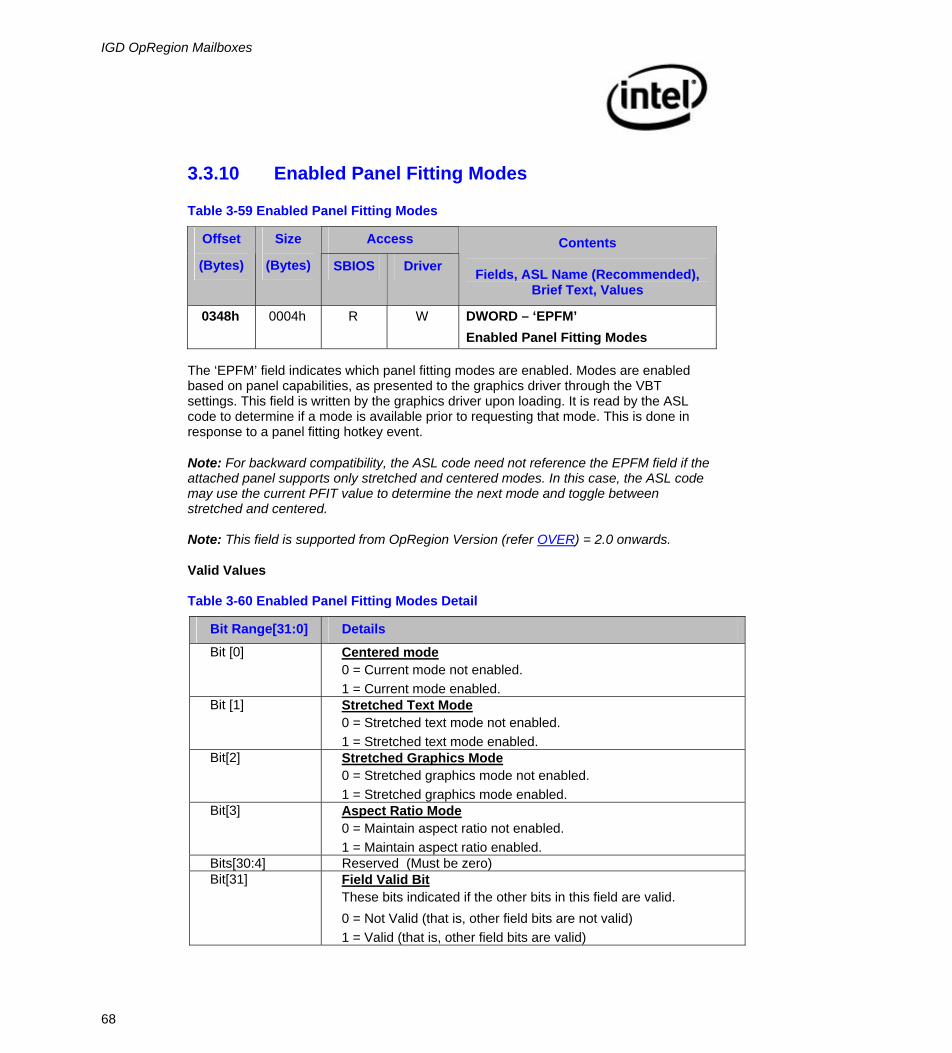
IGD OpRegion Mailboxes
68
3.3.10 Enabled Panel Fitting Modes
Table 3-59 Enabled Panel Fitting Modes
Access Offset
(Bytes)
Size
(Bytes) SBIOS Driver Contents
Fields, ASL Name (Recommended), Brief Text, Values
0348h 0004h R W DWORD – ‘EPFM’ Enabled Panel Fitting Modes
The ‘EPFM’ field indicates which panel fitting modes are enabled. Modes are enabled based on panel capabilities, as presented to the graphics driver through the VBT settings. This field is written by the graphics driver upon loading. It is read by the ASL code to determine if a mode is available prior to requesting that mode. This is done in response to a panel fitting hotkey event. Note: For backward compatibility, the ASL code need not reference the EPFM field if the attached panel supports only stretched and centered modes. In this case, the ASL code may use the current PFIT value to determine the next mode and toggle between stretched and centered. Note: This field is supported from OpRegion Version (refer OVER) = 2.0 onwards. Valid Values
Table 3-60 Enabled Panel Fitting Modes Detail
Bit Range[31:0] Details Bit [0] Centered mode
0 = Current mode not enabled. 1 = Current mode enabled.
Bit [1] Stretched Text Mode 0 = Stretched text mode not enabled. 1 = Stretched text mode enabled.
Bit[2] Stretched Graphics Mode 0 = Stretched graphics mode not enabled. 1 = Stretched graphics mode enabled.
Bit[3] Aspect Ratio Mode 0 = Maintain aspect ratio not enabled. 1 = Maintain aspect ratio enabled.
Bits[30:4] Reserved (Must be zero) Bit[31] Field Valid Bit
These bits indicated if the other bits in this field are valid. 0 = Not Valid (that is, other field bits are not valid) 1 = Valid (that is, other field bits are valid)

IGD OpRegion Mailboxes
69
3.3.11 Panel LUT and Identifier
For EDID-less panels, the OEM has the responsibility of loading the right LUT for the panel.
For any type of panel, an SBIOS ACPI OpRegion based approach is possible where the SBIOS indicates the LCD panel identifier and the LUT (optionally) through the OpRegion mailbox #3 (ASLE communication mailbox). Because the first and last row of LUT will be 0 and 255 respectively, they need not be stored in a mailbox. This translates to 7x9 = 63 bytes of mailbox space. A header will be there for the panel identifier and LUT. This will be followed by the 10 byte panel identifier and an optional LUT of 63 bytes. The panel identifier is of the same format as used by EDID 1.3.
Note: PLUT is supported from OpRegion Version (refer OVER) = 2.0 onwards.
Table 3-61 Panel and LUT Identifier
Access Offset
(Bytes)
Size
(Bytes) SBIOS Driver
Contents
Fields, ASL Name (Recommended), Brief Text, Values
034Ch 0001h R/W R LUT Header 034Dh 000Ah R/W R Panel Identifier 0357h 003Fh R/W R LUT Table of 7x9 – Rows indicates old gray
levels, column indicates new gray levels.
Valid Values LUT Header: LUT Header details
Bit Range[7:0] Details Bits[0] Use System BIOS Panel Identifier
If this bit is set, and the panel is non-EDID, the identifier in next byte will be used while building the fake EDID.
Bit[1]
Override EDID Panel Identifier If this bit is set and panel has EDID, this will create a fake EDID which has the panel identifier from next byte and timings information from the actual EDID.
Bit[2] LUT Valid If this bit is set, the LUT table is valid
Bit[3] Overwrite registry LUT (if any) If this bit is set, overwrite the LUT data from the registry (if any)
Bit[4:7] Reserved
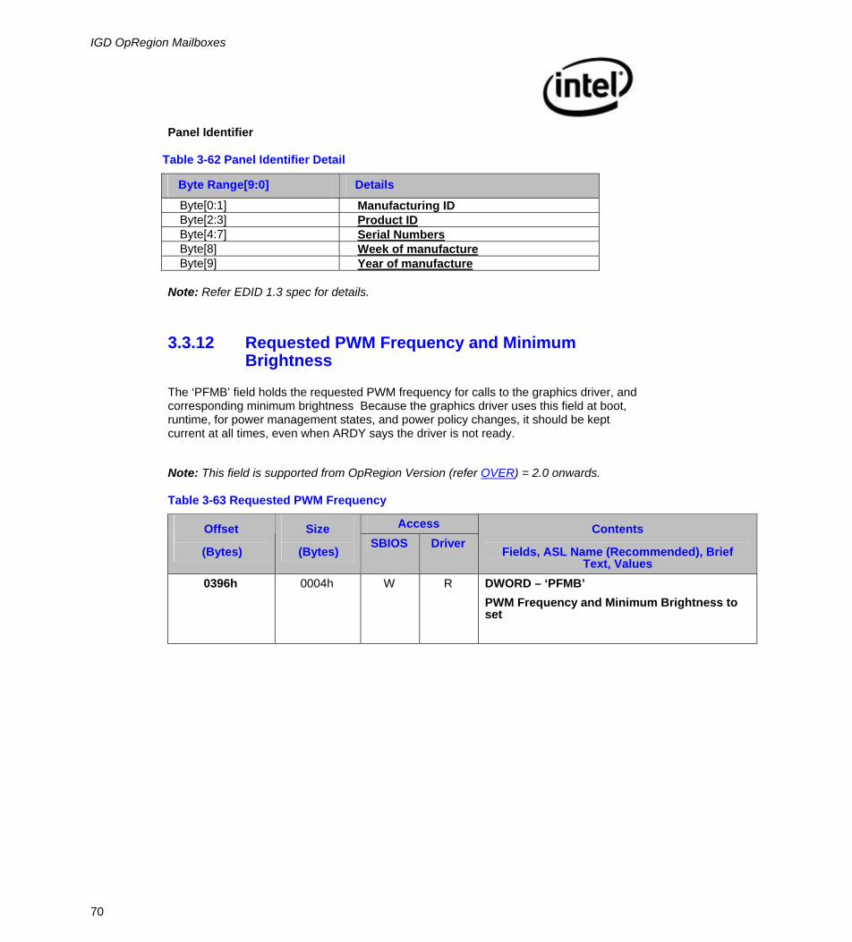
IGD OpRegion Mailboxes
70
Panel Identifier
Table 3-62 Panel Identifier Detail
Byte Range[9:0] Details Byte[0:1] Manufacturing ID Byte[2:3] Product ID Byte[4:7] Serial Numbers Byte[8] Week of manufacture Byte[9] Year of manufacture
Note: Refer EDID 1.3 spec for details.
3.3.12 Requested PWM Frequency and Minimum Brightness
The ‘PFMB’ field holds the requested PWM frequency for calls to the graphics driver, and corresponding minimum brightness Because the graphics driver uses this field at boot, runtime, for power management states, and power policy changes, it should be kept current at all times, even when ARDY says the driver is not ready.
Note: This field is supported from OpRegion Version (refer OVER) = 2.0 onwards.
Table 3-63 Requested PWM Frequency
Access Offset
(Bytes)
Size
(Bytes) SBIOS Driver
Contents
Fields, ASL Name (Recommended), Brief Text, Values
0396h 0004h W R DWORD – ‘PFMB’ PWM Frequency and Minimum Brightness to set
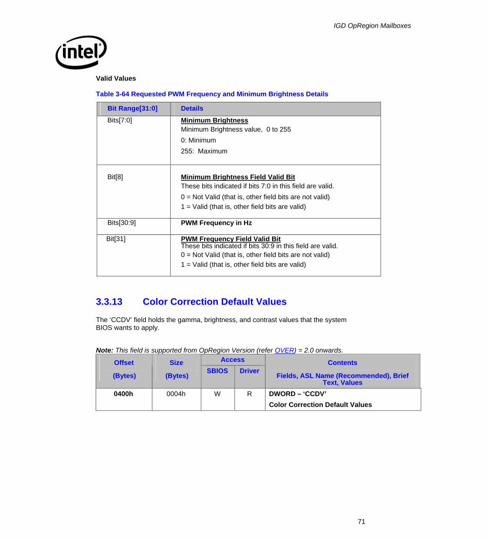
IGD OpRegion Mailboxes
71
Valid Values
Table 3-64 Requested PWM Frequency and Minimum Brightness Details
Bit Range[31:0] Details Bits[7:0] Minimum Brightness
Minimum Brightness value, 0 to 255 0: Minimum 255: Maximum
Bit[8]
Minimum Brightness Field Valid Bit These bits indicated if bits 7:0 in this field are valid. 0 = Not Valid (that is, other field bits are not valid) 1 = Valid (that is, other field bits are valid)
Bits[30:9] PWM Frequency in Hz
Bit[31] PWM Frequency Field Valid Bit These bits indicated if bits 30:9 in this field are valid. 0 = Not Valid (that is, other field bits are not valid) 1 = Valid (that is, other field bits are valid)
3.3.13 Color Correction Default Values
The ‘CCDV’ field holds the gamma, brightness, and contrast values that the system BIOS wants to apply.
Note: This field is supported from OpRegion Version (refer OVER) = 2.0 onwards.
Access Offset
(Bytes)
Size
(Bytes) SBIOS Driver
Contents
Fields, ASL Name (Recommended), Brief Text, Values
0400h 0004h W R DWORD – ‘CCDV’ Color Correction Default Values

IGD OpRegion Mailboxes
72
Valid Values
Table 3-65 Color Correction Default Values Details
Bit Range[31:0] Details Bits[6:0] Gamma Value
This value indicates actual gamma value * 10. Range of the value is from 10 to 50. (for actual gamma range from 0.1 to 0.5)
Bit[7] Gamma Field Valid Indicates whether there is a valid Gamma value specified or not. = 0 Gamma Value not specified = 1 Gamma Value specified Note: If this bit is not set to ‘1’, the system BIOS should ignore the Gamma value, that is Bit[6:0]
Bit[14:8] Brightness Value This value indicates actual brightness value + 60. The range of the value is from 0 to 160. (for actual brightness range from -60 to 100)
Bit[15] Brightness Field Valid Indicates whether there is a valid Brightness value specified or not. = 0 Brightness Value not specified = 1 Brightness Value specified Note: If this bit is not set to ‘1’, the system BIOS should ignore the Brightness
value, that is Bit[14:8] Bits[22:16] Contrast Value
This value contains the actual contrast value. The range of the value is 40 to 100. Bit[23] Contrast Field Valid
Indicates whether there is a valid Contrast value specified or not. = 0 Contrast Value not specified = 1 Contrast Value specified Note: If this bit is not set to ‘1’, the system BIOS should ignore the Contrast value,
that is Bit[22:16] Bit[31:24] Reserved
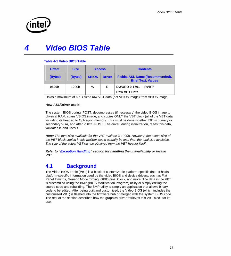
Video BIOS Table
73
4 Video BIOS Table Table 4-1 Video BIOS Table
Access Offset
(Bytes)
Size
(Bytes) SBIOS Driver
Contents
Fields, ASL Name (Recommended), Brief Text, Values
0500h 1200h W
R DWORD 0-1791 – ’RVBT’ Raw VBT Data
Holds a maximum of 6 KB sized raw VBT data (not VBIOS image) from VBIOS image. How ASL/Driver use it: The system BIOS during, POST, decompresses (if necessary) the video BIOS image to physical RAM, scans VBIOS image, and copies ONLY the VBT block (all of the VBT data including its header) to OpRegion memory. This must be done whether IGD is primary or secondary VGA, and after VBIOS POST. The driver, during initialization, reads this data, validates it, and uses it. Note: The total size available for the VBT mailbox is 1200h. However, the actual size of the VBT block copied in this mailbox could actually be less than the total size available. The size of the actual VBT can be obtained from the VBT header itself. Refer to “Exception Handling” section for handling the unavailability or invalid VBT.
4.1 Background The Video BIOS Table (VBT) is a block of customizable platform-specific data. It holds platform-specific information used by the video BIOS and device drivers, such as Flat Panel Timings, Generic Mode Timing, GPIO pins, Clock, and more. The data in the VBT is customized using the BMP (BIOS Modification Program) utility or simply editing the source code and rebuilding. The BMP utility is simply an application that allows binary code to be edited. After being built and customized, the Video BIOS (which includes the customized VBT) is flashed into the firmware hub or merged with the system BIOS code. The rest of the section describes how the graphics driver retrieves this VBT block for its use.
Video BIOS Table
74
4.2 Requirements Summary The following table lists the VBT fetching requirements for the system BIOS and graphics drivers supporting the OpRegion model.
Table 4-2 Video BIOS Table Requirements Summary
Requirement System BIOS Graphics Driver
OpRegion Model VBT Fetch method support
Yes Yes
Legacy Model methods support No Yes (for legacy chipsets only)
VBT Region in OpRegion Yes Yes
VBT Region Accessibility Write once by the system BIOS Read
Communication with Video BIOS
No No
VBT Fetching Method Scan/Copy from FWH to VBT Region in OpRegion
Get from VBT Region in OpRegion
VBT Fetch in Primary & Secondary VGA IGD adapter modes
Yes Yes
VBT Fetch Time During system BIOS POST During Driver Initialization
VBT Fetch during S-state transitions
S5->S0 and S4->S0 (Support scenario where user may discard hibernate data and boot normally)
S5->S0
VBT Modification at run-time No (just loaded once by system BIOS)
No
4.3 VBT Retrieval Methods The system BIOS needs to implement a VBT retrieval method that conforms to this specification – OpRegion Method. However, the graphics drivers need to support both the OpRegion method, as well as legacy methods, because the graphics driver stack being a unified driver stack, needs to be backwards compatible with legacy implementations. The following subsection describes the OpRegion VBT retrieval method only.
Video BIOS Table
75
4.4 OpRegion Method In the OpRegion model, the driver retrieves the VBT block using a single method, regardless of whether IGD is a primary or secondary VGA device. This is accomplished by obtaining the VBT block using the Memory OpRegion VBT region that is set up with the VBT block by the system BIOS during its POST.

Legacy and Exception Handling
76
5 Legacy and Exception Handling This section identifies some of the potential failure scenarios and recommends the course of action described below.
5.1 No ACPI OpRegion Support The following failure scenarios result in non-ACPI OpRegion framework:
• ‘0’ in ASLS register means that the ACPI OpRegion is not supported in the platform or
• Non-zero in ASLS register but an invalid signature (SIGN) in OpRegion Header In this case, the graphics driver should attempt to use legacy methods, if available. Refer to the appropriate subsections below for instructions on handling the worst case failure scenarios.
5.2 Partial Mailbox support Technically, this is not a failure scenario, as per the description of mailbox support field () in the OpRegion Header. So, this section details handling the case of unsupported mailboxes.
a) No support for mailbox #1: Public ACPI Methods (MBOX[0] = 0)
The graphics driver reverts back to legacy methods of interacting with system firmware. However, if the legacy methods involve SMI, the graphics driver may need to disable the features that are dependent on the public ACPI methods. Basically, the worst case scenario is to run the graphics driver on reduced feature mode.
b) No support for mailbox #2: SWSC I (MBOX[1] = 0)
The SWSCI feature will not be available for the graphics driver. This means that some of the features in mobile platforms may not be available or feature set customizations may not be working.
For example, BIOS boot display persistence may not work because the feature to update the CMOS value is not available.
c) No support for mailbox #3 : Power conservation functionality (MBOX[2] = 0) The graphics driver reverts back to legacy methods of interacting with system firmware. However, if the legacy methods involve SMI, the graphics driver may need to disable the features that are dependent on the power conservation. Basically, the worst case scenario is to run the graphics driver on reduced feature mode.

Legacy and Exception Handling
77
5.3 Invalid VBT Even though the VBT is defined as mandatory in the Memory OpRegion, the failure could be because of corruption or an invalid VBT header. The impact of unavailability of VBT will be handled differently between desktop and mobile platforms, as explained below:
Desktop: The graphics driver uses the default values for the features and parameters otherwise customized through VBT. This could result in graphics subsystem behavior different from that of the OEM-customized platform behavior. Mobile: As some mobile platforms are totally dependent on the VBT for driving the local flat panels, depending on the current configuration and attached display devices, it may either be unloaded or switch to a different display device with an error log generated. In cases possible, like for example an EDID-based LFP, the graphics driver may handle it like a desktop system, as explained above. The VBT override through INF will still happen if the driver default values are assumed.

Public ACPI Methods
78
6 Public ACPI Methods Public ACPI methods with video implications fall under two categories:
1) ACPI Video Extensions - provides video-specific mechanisms for the purpose of:
• Enhancing video drivers with ACPI capabilities • Involving drivers, system ACPI BIOS, and OS together in the event or decision
process
2) ACPI Platform support with video implications – provides mechanisms that have platform-wide impact, including video, such as reporting: • Lid state change • Dock or undock event
6.1 ACPI Requirements Refer to ACPI Video Extensions 1.0b/2.0c/3.0 specification for ACPI requirements. The following table merely highlights all the display methods, as mentioned in the ACPI 1.0b/2.0c/3.0 specification.
Table 6-1 ACPI Video Extension Requirements
ACPI Video Extensions
Method Adapter/ Display
Description ACPI Spec Support/ Requirement
_DOS Adapter Enable/Disable output device switching
>=1, R
_DOD Adapter Enumerate all devices >=1, R
_ROM Adapter Get ROM data >=1, O
_GPD Adapter Get POST device >=2, R (if _VPO implemented)
_SPD Adapter Set POST device >=2, R (if _VPO implemented)
_VPO Adapter Video POST options >=2, R (if system supports changing POST VGA device)

Public ACPI Methods
79
ACPI Video Extensions
Method Adapter/ Display
Description ACPI Spec Support/ Requirement
_ADR Output-specific Unique ID for an output >=1, R
_BCL Output-specific Query supported brightness levels
>=1, O (1), R (>=2)
_BCM Output-specific Set brightness level >=1, R if _BCL supported
_BQC Output-specific Query current brightness level
=3, R(?) if _BCL supported
_DDC Output-specific Return EDID >=1, O
_DCS Output-specific Return status >=1, R
_DGS Output-specific Query graphics state >=1, O
_DSS Output-specific Device set state >=1, O
ACPI Non-Video Extensions – LID support
_LID Other Report lid state >=1, O
ACPI Non-Video Extensions – ALS support
_ALC Other Current ambient light color chromaticity
3, O
_ALI Other Current ambient light brightness 3, O
_ALP Other Ambient light sensor polling frequency
3, O
_ALR Other Return mapping of Ambient light brightness to display brightness
3, O
_ALT Other Ambient light color temp 3, O Method – Refers to an ACPI object or method 1 – ACPI 1.0b specification method 2 – ACPI 2.0c specification method 3 – ACPI 3.0 specification method R – Required method O – Optional method
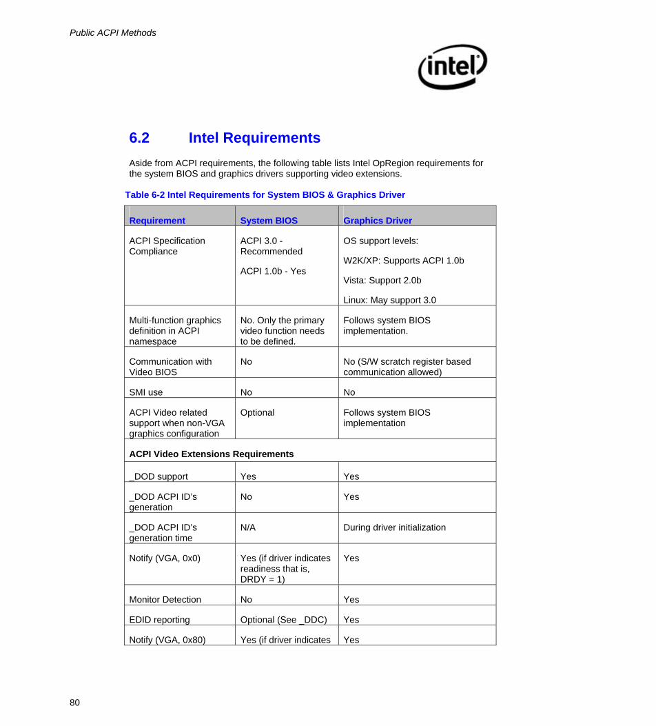
Public ACPI Methods
80
6.2 Intel Requirements Aside from ACPI requirements, the following table lists Intel OpRegion requirements for the system BIOS and graphics drivers supporting video extensions.
Table 6-2 Intel Requirements for System BIOS & Graphics Driver
Requirement System BIOS Graphics Driver
ACPI Specification Compliance
ACPI 3.0 - Recommended
ACPI 1.0b - Yes
OS support levels:
W2K/XP: Supports ACPI 1.0b
Vista: Support 2.0b
Linux: May support 3.0
Multi-function graphics definition in ACPI namespace
No. Only the primary video function needs to be defined.
Follows system BIOS implementation.
Communication with Video BIOS
No No (S/W scratch register based communication allowed)
SMI use No No
ACPI Video related support when non-VGA graphics configuration
Optional Follows system BIOS implementation
ACPI Video Extensions Requirements
_DOD support Yes Yes
_DOD ACPI ID’s generation
No Yes
_DOD ACPI ID’s generation time
N/A During driver initialization
Notify (VGA, 0x0)
Yes (if driver indicates readiness that is, DRDY = 1)
Yes
Monitor Detection No Yes
EDID reporting Optional (See _DDC) Yes
Notify (VGA, 0x80) Yes (if driver indicates Yes
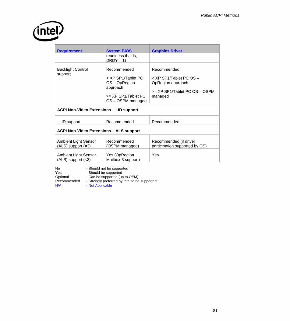
Public ACPI Methods
81
Requirement System BIOS Graphics Driver
readiness that is, DRDY = 1)
Backlight Control support
Recommended
< XP SP1/Tablet PC OS – OpRegion approach
>= XP SP1/Tablet PC OS – OSPM managed
Recommended
< XP SP1/Tablet PC OS – OpRegion approach
>= XP SP1/Tablet PC OS – OSPM managed
ACPI Non-Video Extensions – LID support
_LID support Recommended Recommended
ACPI Non-Video Extensions – ALS support
Ambient Light Sensor (ALS) support (=3)
Recommended (OSPM managed)
Recommended (if driver participation supported by OS)
Ambient Light Sensor (ALS) support (<3)
Yes (OpRegion Mailbox-3 support)
Yes
No - Should not be supported Yes - Should be supported Optional - Can be supported (up to OEM) Recommended - Strongly preferred by Intel to be supported N/A - Not Applicable
Public ACPI Methods
82
6.3 Driver Readiness The driver may not be ready (OpRegion[DRDY] = 0) for ACPI notifications from the system BIOS in the following scenarios:
• Overlay playback is in progress and the VBT option indicates not to perform
display detection or display switching • 3D app is running and VBT option indicates not to perform display detection
or display switching • The driver is not loaded or yet to initialize the adapter or is processing an
adapter power state transition • The system in FSDOS and VBT option is to block display switching • GMBUS ports/GPIO/I2C pins that are required for any communication with
monitors or attached encoders are unavailable: o Ports are locked for trusted graphics operation o Another process is currently using these ports such as the driver is in the
middle of an MCCS transaction.
The system BIOS should always check if OpRegion[DRDY] = 1 condition before issuing any non-critical graphics notification. However, the system BIOS can continue to access OpRegion under such conditions, for example, to update Lqd State. OS notifications that translate to calls into the graphics driver are:
• Notify(0) – Display Enumeration • Notify(0x80) – Display switch
Certain OS notifications that translate into graphics driver calls are critical in nature (system-wide implications) and therefore should be issued regardless of driver readiness. These include reporting:
• Lid events • Dock or Undock events
6.4 Display Enumeration
6.4.1 Background
ACPI-based display enumeration is a process by which the ACPI system BIOS, the ACPI OS, and the graphics driver work together to determine display output devices attached to the Intel graphics adapter. This requires both the system BIOS and graphics driver to support ACPI 1.0b video extensions and for the graphics driver to provide a one-time static list of device IDs.
Public ACPI Methods
83
6.4.2 System BIOS Display Re-enumeration Triggers
The system BIOS-initiated enumeration is required in following scenarios: • Hotkey display switching – if hotplug is currently enabled, this notify is not
required. Refer to the ‘Current Hotplug Enable’ indicator for details. • Lid event based display switching – A lid closure or open does not generate
a hotplug interrupt. Therefore, such events need to be communicated to the graphics driver prior to display switching process. Refer to ‘Current Lid State’ indicator for further details.
• Dock/Undock events – Dock designs typically do not support hotplug of monitors. This is just one reason why re-enumeration is mandatory (regardless of ‘Current Hotplug Enable’ indicator setting).
6.4.3 Requirements
Relevant ACPI 1.0b Video Extension Display Specific Methods per IGD Display Device (function) defined in ACPI namespace are:
• _DOD (Mandatory) – Enumerate connectors • _DOS (Optional) – Enable or disable display switching
Relevant ACPI 1.0b Video Extension ASL Objects/Methods per output device packaged using _DOD in IGD ACPI namespace are:
• _ADR – Per graphics output device, provides 1 unique ID per output device packaged using _DOD
• _DDC (Optional and not recommended) – Report EDID
Relevant ACPI 1.0b Video Extensions ASL->OS notification codes in graphics device scope are:
• 0x0 – Notify OS to perform display enumeration
Relevant OpRegion fields for the system BIOS if the system BIOS issues notify(0) are:
• DRDY • CSTS • CHPD • CNOT • ASLP
Relevant OpRegion fields for the system BIOS _DOD method are:
• DIDL
Relevant OpRegion fields for the system BIOS _DOS method are:
None
Public ACPI Methods
84
Relevant OpRegion fields for the system BIOS _DDC method are:
None
Relevant OpRegion fields for the graphics driver are:
• CSTS (if the system BIOS triggered notification) • DIDL • CPDL • NADL
If the system BIOS initiates enumeration of its own accord, it should do so only if the driver is ready, that is, OpRegion[DRDY] = 1.
6.4.4 Display Enumeration Types
There are three broad types for triggering the display enumeration process, all of which are detailed below:
• Operating System initiated enumeration • System BIOS or graphics driver initiated enumeration • User initiated enumeration
6.4.4.1 Operating System Initiated Enumeration
The ACPI kernel can initiate enumeration of its own accord under the following circumstances:
• During OS boot prior to graphics driver load – ACPI OS evaluates _DOD method
prior to graphics driver load. This is not a typical case, but in the event _DOD is invoked prior to driver load, _DOD should return 0 as the number of packaged devices.
• During OS boot after graphics driver load – ACPI OS evaluates _DOD method
and using the returned attachable display device ID list, calls the graphics driver to determine what display devices are actually attached (and EDID info). A special case of enumeration is in response to a dock or undock OS notification from the system BIOS where the ACPI OS may additionally translate this notification into _DOD evaluation and a call to the graphics driver, to provide EDID for its display devices.
Public ACPI Methods
85
6.4.4.2 System BIOS/Graphics Driver Initiated Enumeration
The system BIOS can also notify the ACPI OS to explicitly perform display device re-enumeration. Enumeration may be triggered by ASL additionally to process, say a hotkey display switch press or coming out a low power state (The OS does not automatically perform display re-enumeration in this case). This notification causes the OS to evaluate _DOD and call the graphics driver to obtain EDIDs for the enumerated display devices.
Refer to “Re-enumeration ACPI notification Issues” for the correct notification method to be used by the ASL code.
Note: The system BIOS notification to the OS should only occur if the graphics driver is ready (OpRegion[DRDY] = 1) to process that notification. In the event that the graphics driver is not ready (DRDY = 0), the system BIOS should not issue Notify (VGA, 0) to the OS.
The graphics driver can also instruct the OS (Videoport/ACPI driver) to call back the driver to re-enumerate display devices. See DDK “VideoPortEnumerateChildren ()” for details. This can happen any time the graphics driver “detects” a change in attached display devices either in response to a hotplug/unplug interrupt or periodic polling of attached display devices. The OS notification is performed so that the OS and the graphics driver are in sync as to what display devices are attached. Synchronization is necessary for plug and play and power management, involving such display devices. This OS API, when invoked, results in _DOD evaluation and a call into the graphics driver for the OS to obtain EDID information for the enumerated display devices.
6.4.4.3 User Initiated Enumeration
The user can also initiate re-enumeration in an OS-specific way. This should cause _DOD to be evaluated by the ACPI OS along with a call to the graphics driver for the OS to obtain EDID information for the enumerated display devices.

Public ACPI Methods
86
6.4.5 Typical Enumeration Flow
The diagram below illustrates a typical display enumeration process.
Figure 6-1 Display Enumeration Flow
OS Display Server
Intel Graphics
Driver
Gfx Display H/W (Intel)
ACPI ASL(IBV/OEM)
Memory OpRegion(Intel)
6. Display server calls graphics driver monitor detection function
5. ASL packages ID’s and returns package to display server
2. _DOS = 2, disable display change
8. Graphics driver performs I2C cycles to fetch EDID or performs other means of device detection.
3. _DOD, get attached devices
11. Display server creates monitor
structures
Enumeration initiated by 1) User2) OS during driver load3) ASL (e.g. display switch hotkey)
Step 1
12. _DOS = 0, enable display change
10. Graphics driver either indicates Monitor w/ EDID presence or Monitor w/o EDID presence or No monitor
9. Graphics driver updates relevant fields incl. completion status in OpRegion.
4. ASL reads memory opregion fields to obtain ID’s
7. Graphics driver indicates status = pending in OpRegion.
Public ACPI Methods
87
6.4.6 EDID Reporting
Operating systems typically rely on the graphics driver to provide description of monitor, typically through EDID. On non-ACPI aware OSs, if the OS does not expose a mechanism for the graphics driver to report EDID, the system BIOS can optionally expose _DDC method. However, this is discouraged.
6.5 Display Switch The ACPI display switch can only be initiated by the system BIOS. It may be initiated in response to the user pressing a display switch hotkey or to the user opening or closing a lid.
6.5.1 Background
The ACPI-based hotkey/lid display switch is a process by which the ACPI system BIOS, the ACPI OS and the graphics driver work together to determine the next display combination to switch to and perform the actual switch to the next display combination. This requires both the system BIOS and the graphics driver to support ACPI 1.0b video extensions and OEM customizable VBT toggle table that provides the supported display device combinations to which they can be switched.
Relevant ACPI 1.0b Video Extension ASL Methods per output display device enumerated using _DOD are:
• _DGS – per output display device packaged by _DOD and enumerated as a valid output device by the graphics driver
• _DOS – graphics device scope
Relevant ACPI 1.0b Video Extensions ASL->OS notification codes in graphics device scope are:
• 0x00 – Notify OS to perform display device re-enumeration • 0x80 – Notify OS to perform display switching
Relevant Memory OpRegion fields are:
• ‘DIDL’ - Supported Display Devices List • ‘CPDL’ - Currently Attached Display Devices List • ‘CADL’ - Currently Active Display Devices List • ‘TIDX’ - Toggle Table Index • ‘NADL’ - Next Active Devices List
A typical display switch flow is depicted in Figure 6-1 Display Enumeration Flow.
Public ACPI Methods
88
6.5.2 Requirements Summary
System BIOS-required changes:
• Relevant ACPI 1.0b Video Extensions ASL->OS notification codes in graphics device scope are:
• 0x80 – Notify OS to perform display switch
• Relevant graphics driver (XPDM) entry points are: • HwVidStartIO() sub functions
• IOCTL_VIDEO_VALIDATE_CHILD_STATE_CONFIGURATION • IOCTL_VIDEO_SET_CHILD_STATE • IOCTL_VIDEO_GET_CHILD_STATE
• Relevant OpRegion fields for system BIOS if system BIOS issues notify(0) are:
• Relevant OpRegion fields for system BIOS _DOS method are:
• Relevant OpRegion fields for system BIOS _DGS method are:
• Relevant OpRegion fields for system BIOS _DCS method are:
• Relevant OpRegion fields for system BIOS _DSS method are:

Public ACPI Methods
89
6.5.3 Typical Display Switch Flow
The diagram below illustrates a typical display switch flow.
Figure 6-2 Display Switch Flow
SWSCI Communication
90
7 SWSCI Communication Video drivers needs to communicate with the system BIOS for various reasons, like:
• Querying Platform/Chipset Capabilities: The driver communicates with the system BIOS to query the platform for chipset specific information, which is usually not available through the PCI configuration space.
• Event Notification: Informing the platform system BIOS on occurrence of display-related events like power management, display switching, mode setting, and others.
The platform can provide unique solution on occurrence of these events. Some of the currently provided platform unique solutions using this information are:
• OEM platform provides an intermediate hardware through which the display device (CRT/Panel) is connected. The power management information is essential to perform that hardware’s power management.
An OEM platform can use this information to provide unique platform solution, not limited to those mentioned above.
• Persisting Display Environment: To maintain the post-OS and pre-OS boot display environment similar, display information needs to be persisted. The post-OS display environment information is stored in non-volatile memory (such as CMOS, Flash, and others) by the driver, with help from the system BIOS. During the next boot, the system BIOS can use this data to set up its pre-OS boot display environment.
To facilitate this communication, protocol and the media are defined as follows:
• Communication Transport Media – the media/transport layer which is o used by the driver to trigger the communication start
used by the system BIOS to identify the communication request and report back the status of the communication.
In the ACPI OpRegion environment, the transport layer used is the SCI interrupt. The next subsections provide details.
• Communication Protocol – the protocol the driver and the system BIOS use to communicate. The protocol is defined in the following subsections.
7.1 SWSCI - The Transport Layer The driver uses SCI interrupt as the communication transport media to communicate with the system BIOS. The details, regarding hardware register for triggering SCI and also the format of programming, will be mentioned in the following topics.
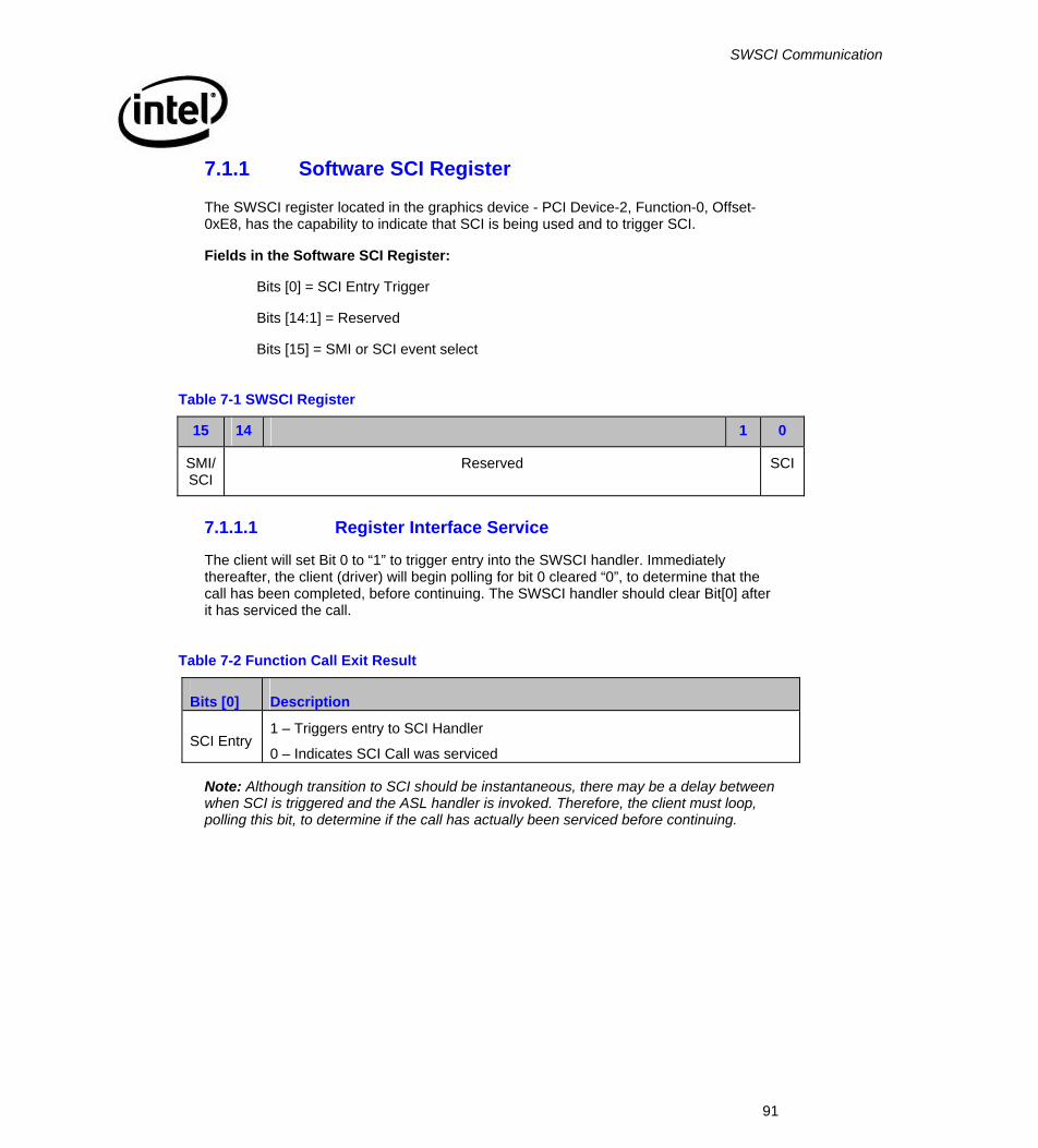
SWSCI Communication
91
7.1.1 Software SCI Register
The SWSCI register located in the graphics device - PCI Device-2, Function-0, Offset-0xE8, has the capability to indicate that SCI is being used and to trigger SCI.
Fields in the Software SCI Register:
Bits [0] = SCI Entry Trigger
Bits [14:1] = Reserved
Bits [15] = SMI or SCI event select
Table 7-1 SWSCI Register
15 14 1 0
SMI/ SCI
Reserved SCI
7.1.1.1 Register Interface Service
The client will set Bit 0 to “1” to trigger entry into the SWSCI handler. Immediately thereafter, the client (driver) will begin polling for bit 0 cleared “0”, to determine that the call has been completed, before continuing. The SWSCI handler should clear Bit[0] after it has serviced the call.
Table 7-2 Function Call Exit Result
Bits [0] Description
SCI Entry 1 – Triggers entry to SCI Handler
0 – Indicates SCI Call was serviced
Note: Although transition to SCI should be instantaneous, there may be a delay between when SCI is triggered and the ASL handler is invoked. Therefore, the client must loop, polling this bit, to determine if the call has actually been serviced before continuing.
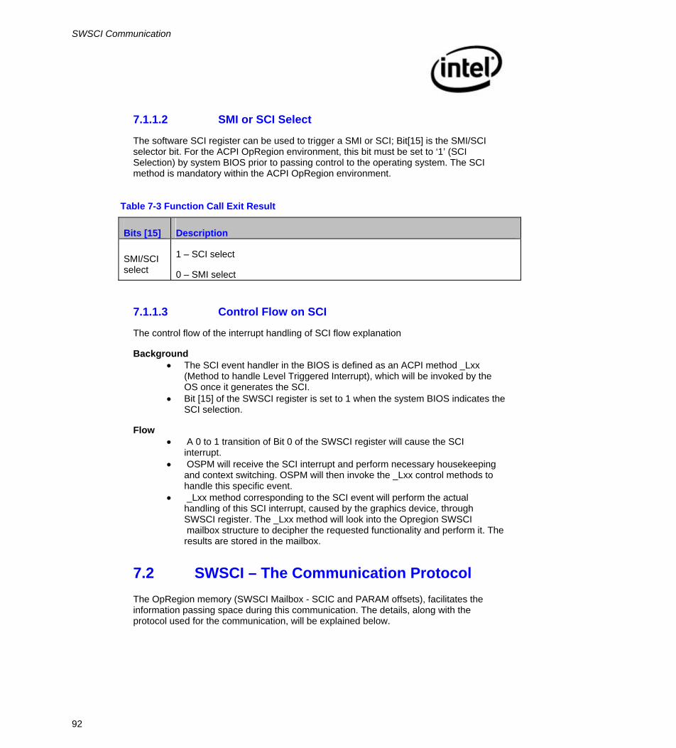
SWSCI Communication
92
7.1.1.2 SMI or SCI Select
The software SCI register can be used to trigger a SMI or SCI; Bit[15] is the SMI/SCI selector bit. For the ACPI OpRegion environment, this bit must be set to ‘1’ (SCI Selection) by system BIOS prior to passing control to the operating system. The SCI method is mandatory within the ACPI OpRegion environment.
Table 7-3 Function Call Exit Result
Bits [15] Description
SMI/SCI select
1 – SCI select
0 – SMI select
7.1.1.3 Control Flow on SCI
The control flow of the interrupt handling of SCI flow explanation
Background • The SCI event handler in the BIOS is defined as an ACPI method _Lxx
(Method to handle Level Triggered Interrupt), which will be invoked by the OS once it generates the SCI.
• Bit [15] of the SWSCI register is set to 1 when the system BIOS indicates the SCI selection.
Flow • A 0 to 1 transition of Bit 0 of the SWSCI register will cause the SCI
interrupt. • OSPM will receive the SCI interrupt and perform necessary housekeeping
and context switching. OSPM will then invoke the _Lxx control methods to handle this specific event.
• _Lxx method corresponding to the SCI event will perform the actual handling of this SCI interrupt, caused by the graphics device, through SWSCI register. The _Lxx method will look into the Opregion SWSCI mailbox structure to decipher the requested functionality and perform it. The results are stored in the mailbox.
7.2 SWSCI – The Communication Protocol The OpRegion memory (SWSCI Mailbox - SCIC and PARAM offsets), facilitates the information passing space during this communication. The details, along with the protocol used for the communication, will be explained below.
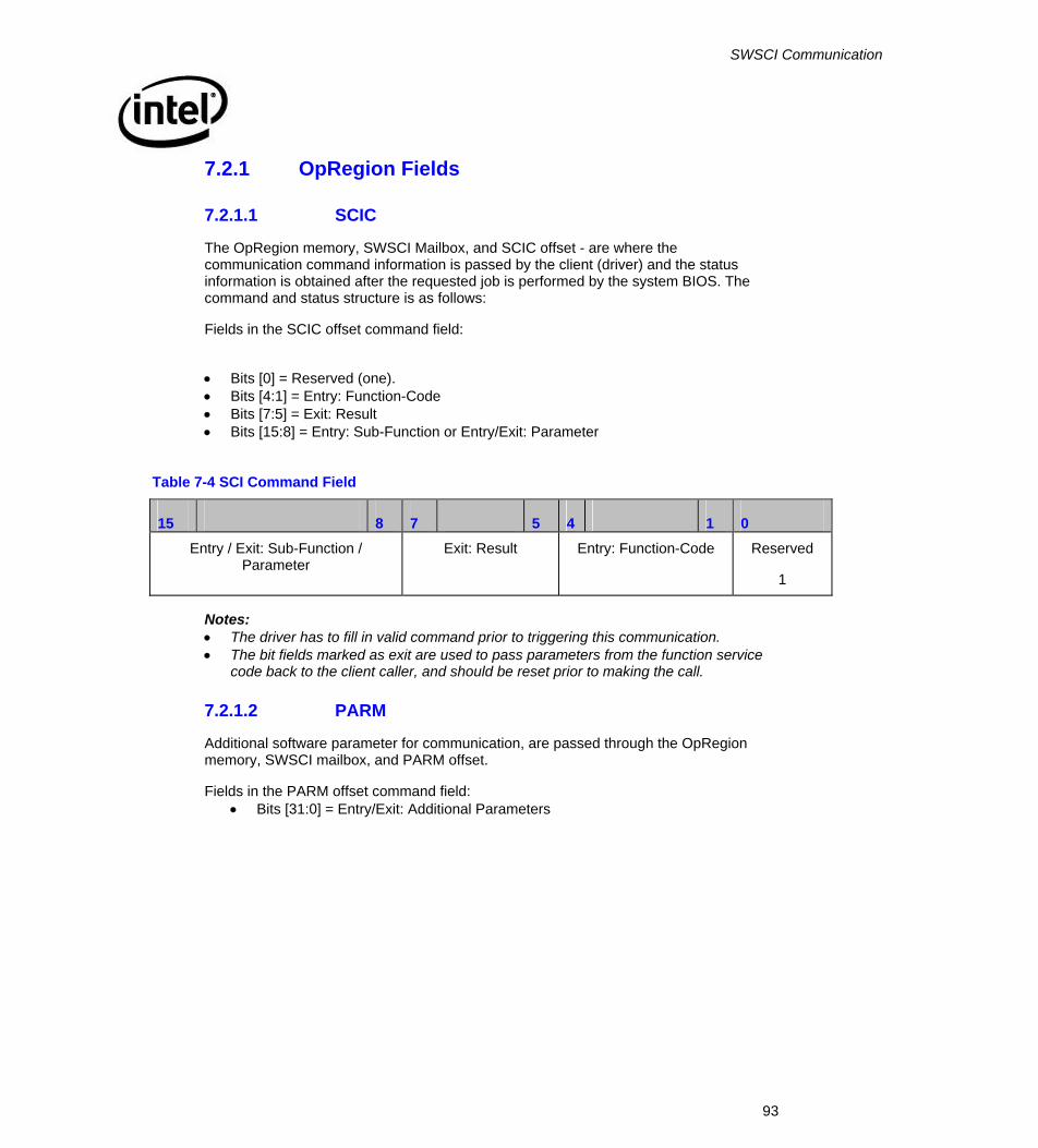
SWSCI Communication
93
7.2.1 OpRegion Fields
7.2.1.1 SCIC
The OpRegion memory, SWSCI Mailbox, and SCIC offset - are where the communication command information is passed by the client (driver) and the status information is obtained after the requested job is performed by the system BIOS. The command and status structure is as follows:
Fields in the SCIC offset command field:
• Bits [0] = Reserved (one). • Bits [4:1] = Entry: Function-Code • Bits [7:5] = Exit: Result • Bits [15:8] = Entry: Sub-Function or Entry/Exit: Parameter
Table 7-4 SCI Command Field
15 8 7 5 4 1 0 Entry / Exit: Sub-Function /
Parameter Exit: Result Entry: Function-Code Reserved
1
Notes: • The driver has to fill in valid command prior to triggering this communication. • The bit fields marked as exit are used to pass parameters from the function service
code back to the client caller, and should be reset prior to making the call.
7.2.1.2 PARM
Additional software parameter for communication, are passed through the OpRegion memory, SWSCI mailbox, and PARM offset.
Fields in the PARM offset command field: • Bits [31:0] = Entry/Exit: Additional Parameters

SWSCI Communication
94
Table 7-5 SCI Parameters
31 0
Additional Parameters
7.2.2 Protocol Overview
7.2.2.1 Interface Function
The entry function is specified in bits [4:1] of the SCIC offset of SWSCI mailbox, and contains the Function-Code for the function call the client wishes to use.
Table 7-6 Protocol Interface Function Codes
Bits [4:1] Description System Requirements Client-Caller Requirements
0-3 Reserved Reserved Reserved
4 Get BIOS Data Some Functions Required Required
5 Reserved Reserved Reserved
6 System BIOS Callbacks Optional
Required if “Requested System Callbacks” indicates implemented
7~15 Reserved Reserved Reserved
7.2.2.2 Interface Sub-Function
Every function call may include sub-functions, which is specific to the functions being invoked. On entry, the client must fill in the subfunction.
Fields in SCIC offset of SWSCI mailbox,
Table 7-7 Function Call Exit Result
Bits [15:8] Description
Subfunction Functional Information or Data Parameters In/Out
Note: On completion, the SCI handler will fill in any return parameters.

SWSCI Communication
95
7.2.2.3 Interface Exit Result
After completing the requested function, the exit result of the communication will be set by the system BIOS. The exit result will contain the success or failure of the interface call.
Fields in SCIC offset of SWSCI mailbox:
Table 7-8 Function Call Exit Result
Bits [7:5] Value Description
1 Success: indicates to the client, that the call was successfully completed.
0 Failure, Generic, Unsupported or Unknown cause
2 Failure, Invalid Parameter
4 Failure, Critical
Exit Result
6 Failure, Non-Critical
Note: This bit is set to all “0” by the client, before the client performs the call. This ensures that the caller clearly understands the return value, and it will be distinguishable from the return value of an incorrect or non-existent SWSCI Handler.
7.2.2.4 Interface Override Policy
Background:
In many circumstances, there are multiple sources of configuration settings, which come from the platform to the graphics software stack from different places. These include:
• Default settings (such as, in the code) • Platform configuration information (such as, in VBT object inside the firmware) • Non-volatile settings (such as, in the RTC CMOS) • OS storage (such as, file or registry) • Run-time user interface changes (such as, CUI)
Typically, the policy for determining which of these settings is applied is derived from the order in which they are processed, as listed above. For example, during driver initialization, a non-volatile memory setting may be overridden by a user setting retrieved by the driver from the OS Registry. If there were no registry setting, then the non-volatile memory setting would persist. Whenever a user interface change is made that is synchronized in the driver, the non-volatile memory and the registry should be updated accordingly. For example, a boot display device setting made by the user through the Intel Common User Interface is passed to the driver and stored in the registry, and the
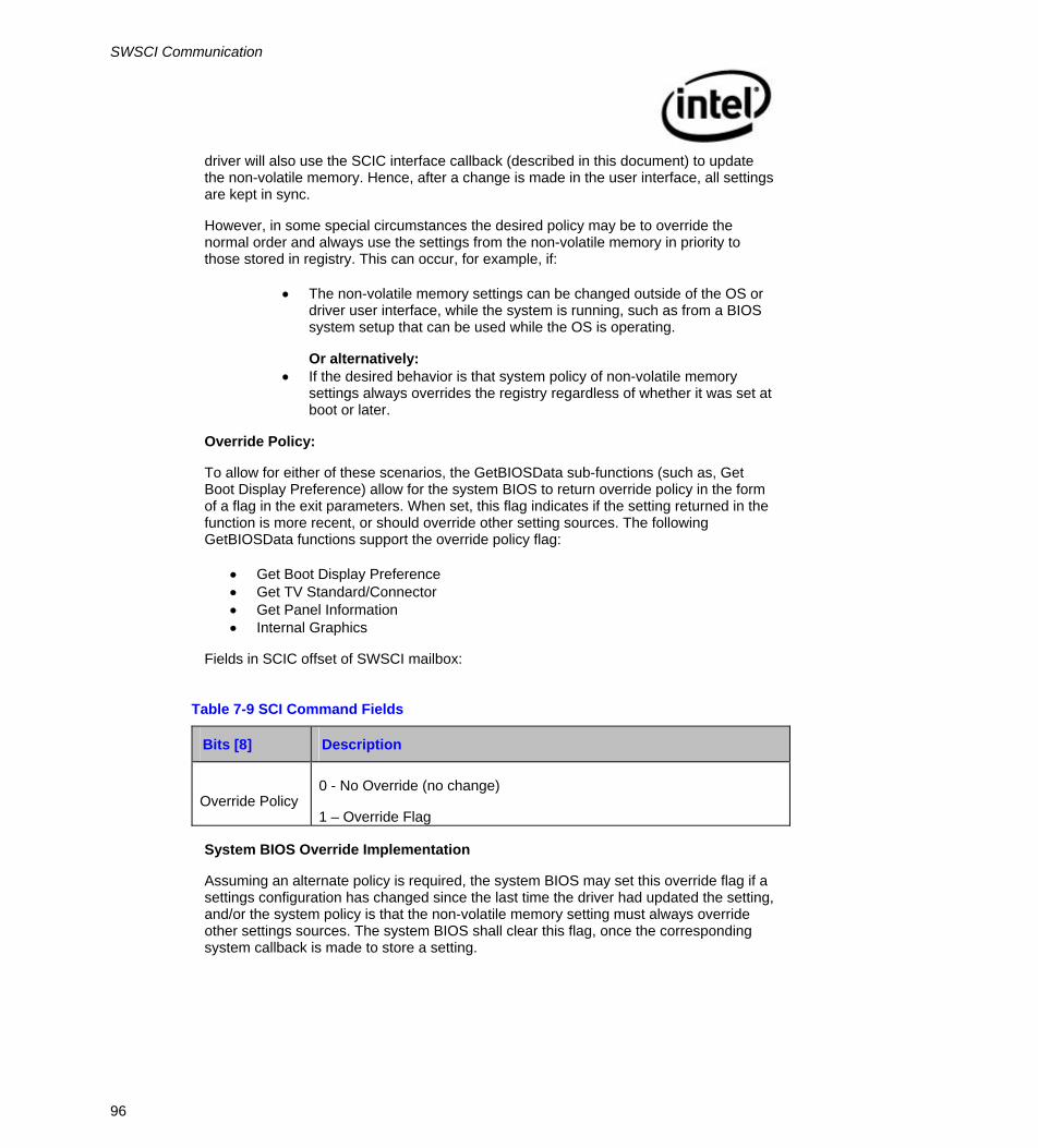
SWSCI Communication
96
driver will also use the SCIC interface callback (described in this document) to update the non-volatile memory. Hence, after a change is made in the user interface, all settings are kept in sync.
However, in some special circumstances the desired policy may be to override the normal order and always use the settings from the non-volatile memory in priority to those stored in registry. This can occur, for example, if:
• The non-volatile memory settings can be changed outside of the OS or
driver user interface, while the system is running, such as from a BIOS system setup that can be used while the OS is operating.
Or alternatively: • If the desired behavior is that system policy of non-volatile memory
settings always overrides the registry regardless of whether it was set at boot or later.
Override Policy:
To allow for either of these scenarios, the GetBIOSData sub-functions (such as, Get Boot Display Preference) allow for the system BIOS to return override policy in the form of a flag in the exit parameters. When set, this flag indicates if the setting returned in the function is more recent, or should override other setting sources. The following GetBIOSData functions support the override policy flag:
• Get Boot Display Preference • Get TV Standard/Connector • Get Panel Information • Internal Graphics
Fields in SCIC offset of SWSCI mailbox:
Table 7-9 SCI Command Fields
Bits [8] Description
Override Policy 0 - No Override (no change)
1 – Override Flag
System BIOS Override Implementation
Assuming an alternate policy is required, the system BIOS may set this override flag if a settings configuration has changed since the last time the driver had updated the setting, and/or the system policy is that the non-volatile memory setting must always override other settings sources. The system BIOS shall clear this flag, once the corresponding system callback is made to store a setting.
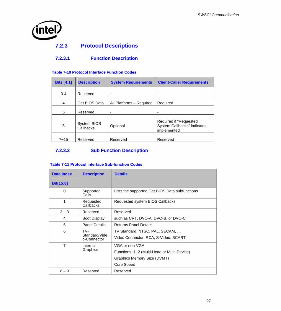
SWSCI Communication
97
7.2.3 Protocol Descriptions
7.2.3.1 Function Description
Table 7-10 Protocol Interface Function Codes
Bits [4:1] Description System Requirements Client-Caller Requirements
0-4 Reserved - -
4 Get BIOS Data All Platforms – Required Required
5 Reserved - -
6 System BIOS Callbacks Optional
Required if “Requested System Callbacks” indicates implemented
7~15 Reserved Reserved Reserved
7.2.3.2 Sub Function Description
Table 7-11 Protocol Interface Sub-function Codes
Data Index
Bit[15:8]
Description Details
0 Supported Calls
Lists the supported Get BIOS Data subfunctions
1 Requested Callbacks
Requested system BIOS Callbacks
2 – 3 Reserved Reserved 4 Boot Display such as CRT, DVO-A, DVO-B, or DVO-C 5 Panel Details Returns Panel Details 6 TV-
Standard/Video-Connector
TV Standard: NTSC, PAL, SECAM, … Video Connector: RCA, S-Video, SCART
7 Internal Graphics
VGA or non-VGA Functions: 1, 2 (Multi-Head or Multi-Device) Graphics Memory Size (DVMT) Core Speed
8 – 9 Reserved Reserved
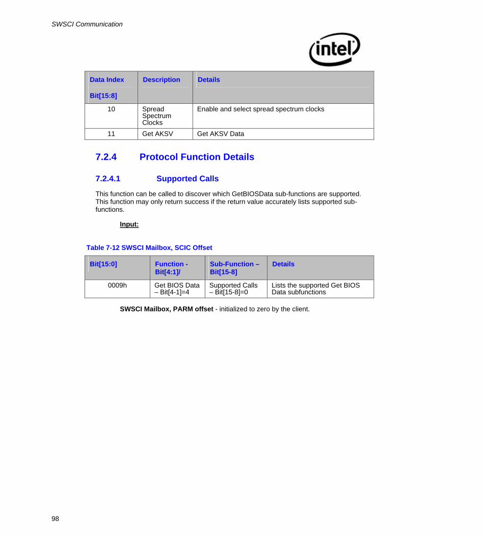
SWSCI Communication
98
Data Index
Bit[15:8]
Description Details
10 Spread Spectrum Clocks
Enable and select spread spectrum clocks
11 Get AKSV Get AKSV Data
7.2.4 Protocol Function Details
7.2.4.1 Supported Calls
This function can be called to discover which GetBIOSData sub-functions are supported. This function may only return success if the return value accurately lists supported sub-functions.
Input:
Table 7-12 SWSCI Mailbox, SCIC Offset
Bit[15:0] Function - Bit[4:1]/
Sub-Function – Bit[15-8]
Details
0009h Get BIOS Data – Bit[4-1]=4
Supported Calls – Bit[15-8]=0
Lists the supported Get BIOS Data subfunctions
SWSCI Mailbox, PARM offset - initialized to zero by the client.
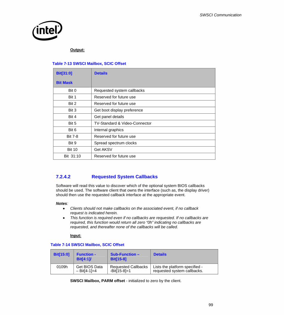
SWSCI Communication
99
Output:
Table 7-13 SWSCI Mailbox, SCIC Offset
Bit[31:0]
Bit Mask
Details
Bit 0 Requested system callbacks Bit 1 Reserved for future use Bit 2 Reserved for future use Bit 3 Get boot display preference Bit 4 Get panel details Bit 5 TV-Standard & Video-Connector Bit 6 Internal graphics
Bit 7-8 Reserved for future use Bit 9 Spread spectrum clocks Bit 10 Get AKSV
Bit 31:10 Reserved for future use
7.2.4.2 Requested System Callbacks
Software will read this value to discover which of the optional system BIOS callbacks should be used. The software client that owns the interface (such as, the display driver) should then use the requested callback interface at the appropriate event.
Notes: • Clients should not make callbacks on the associated event, if no callback
request is indicated herein. • This function is required even if no callbacks are requested. If no callbacks are
required, this function would return all zero “0h” indicating no callbacks are requested, and thereafter none of the callbacks will be called.
Input:
Table 7-14 SWSCI Mailbox, SCIC Offset
Bit[15:0] Function - Bit[4:1]/
Sub-Function – Bit[15-8]
Details
0109h Get BIOS Data – Bit[4-1]=4
Requested Callbacks -Bit[15-8]=1
Lists the platform specified - requested system callbacks.
SWSCI Mailbox, PARM offset - initialized to zero by the client.
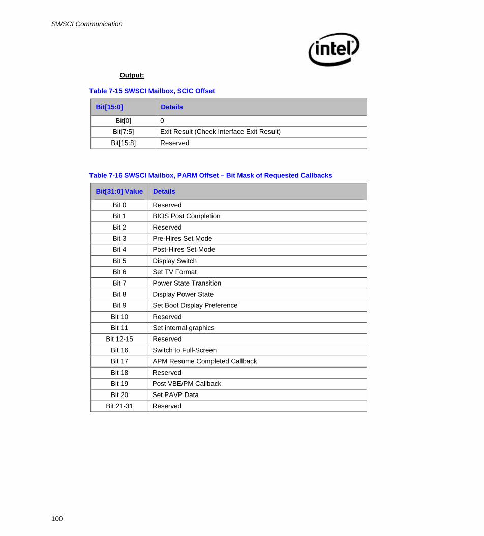
SWSCI Communication
100
Output:
Table 7-15 SWSCI Mailbox, SCIC Offset
Bit[15:0] Details
Bit[0] 0 Bit[7:5] Exit Result (Check Interface Exit Result)
Bit[15:8] Reserved
Table 7-16 SWSCI Mailbox, PARM Offset – Bit Mask of Requested Callbacks
Bit[31:0] Value Details
Bit 0 Reserved Bit 1 BIOS Post Completion Bit 2 Reserved Bit 3 Pre-Hires Set Mode Bit 4 Post-Hires Set Mode Bit 5 Display Switch Bit 6 Set TV Format Bit 7 Power State Transition Bit 8 Display Power State Bit 9 Set Boot Display Preference Bit 10 Reserved Bit 11 Set internal graphics
Bit 12-15 Reserved Bit 16 Switch to Full-Screen Bit 17 APM Resume Completed Callback Bit 18 Reserved Bit 19 Post VBE/PM Callback Bit 20 Set PAVP Data
Bit 21-31 Reserved

SWSCI Communication
101
7.2.4.3 Get Boot Display Preferences
Assuming the GMCH’s internal graphics are enabled, this field will indicate which display device will be the primary boot display device. Only this display will show the video BIOS POST and OS boot screen. Other display devices will be unaffected.
Note that the system BIOS setup may offer the end-user selection using other terms, such as “CRT”, “Local Flat Panel”, “External Flat-Panel”, “Television”, “External Flat-Panel #2”, and so on. With the exception of the Integrated CRT, or Integrated LVDS, these options typically do not have a fixed relationship to Display-Ports, and are platform-implementation-specific – the caller: VBIOS or driver, will pass-in the known supported associations in the Display Port Device Type Mask.
In the case where one display port can support multiple displays (such as from a DVI/TV combination encoder, or “Combo Codec”), the input fields for the “Port Display Device Type” masks will indicate all of the display types supported by the encoder on the display port, on an individual basis.
If the system BIOS returns a Dual-Display Simultaneous (Twin/Clone) configuration, the selection of Primary Boot Display Device may be returned using PARM bits [15:13]. The primary display is the one from which the simultaneous mode and timings (in the case of Dual-Display Twin) are derived. This field does not need to be saved, or returned if ability to select a different primary device is not required. In that case, a value of zero ‘0’ (use defaults) can be passed.
Input:
Table 7-17 SWSCI Mailbox, SCIC Offset
Bit[15:0] Function - Bit[4:1]/
Sub-Function – Bit[15-8]
Details
0409h Get BIOS Data – Bit[4-1]=4
Get Boot Display Preference -Bit[15-8]=4
Returns the display boot display preference.
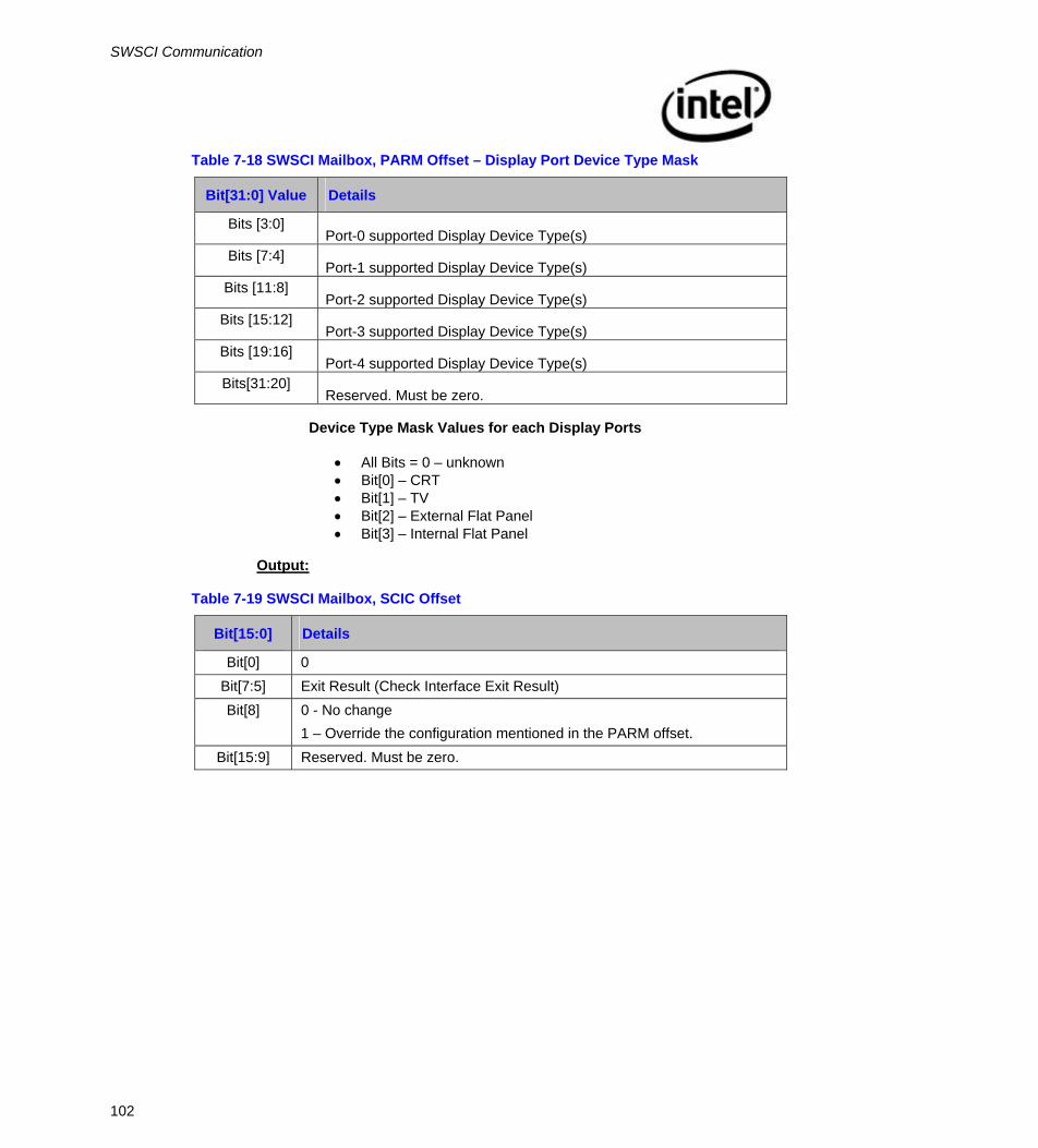
SWSCI Communication
102
Table 7-18 SWSCI Mailbox, PARM Offset – Display Port Device Type Mask
Bit[31:0] Value Details
Bits [3:0] Port-0 supported Display Device Type(s)
Bits [7:4] Port-1 supported Display Device Type(s)
Bits [11:8] Port-2 supported Display Device Type(s)
Bits [15:12] Port-3 supported Display Device Type(s)
Bits [19:16] Port-4 supported Display Device Type(s)
Bits[31:20] Reserved. Must be zero.
Device Type Mask Values for each Display Ports
• All Bits = 0 – unknown • Bit[0] – CRT • Bit[1] – TV • Bit[2] – External Flat Panel • Bit[3] – Internal Flat Panel
Output:
Table 7-19 SWSCI Mailbox, SCIC Offset
Bit[15:0] Details
Bit[0] 0 Bit[7:5] Exit Result (Check Interface Exit Result) Bit[8] 0 - No change
1 – Override the configuration mentioned in the PARM offset. Bit[15:9] Reserved. Must be zero.
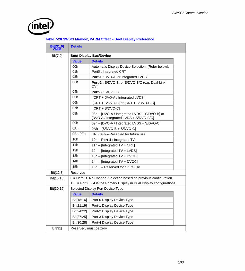
SWSCI Communication
103
Table 7-20 SWSCI Mailbox, PARM Offset – Boot Display Preference
Bit[31:0] Value
Details
Bit[7:0] Boot Display Bus/Device Value Details 00h Automatic Display Device Selection. (Refer below). 01h Port0 : Integrated CRT 02h Port-1 : DVO-A, or Integrated LVDS 03h Port-2 : S/DVO-B, or S/DVO-B/C (e.g. Dual-Link
DVI) 04h Port-3 : S/DVO-C 05h [CRT + DVO-A / Integrated LVDS] 06h [CRT + S/DVO-B] or [CRT + S/DVO-B/C] 07h [CRT + S/DVO-C] 08h 08h – [DVO-A / Integrated LVDS + S/DVO-B] or
[DVO-A / Integrated LVDS + S/DVO-B/C] 09h 09h – [DVO-A / Integrated LVDS + S/DVO-C] 0Ah 0Ah – [S/DVO-B + S/DVO-C] 0Bh-0Fh 0A ~ 0Fh – Reserved for future use. 10h 10h – Port-4 : Integrated TV 11h 11h – [Integrated TV + CRT] 12h 12h – [Integrated TV + LVDS] 13h 13h – [Integrated TV + DVOB] 14h 14h – [Integrated TV + DVOC] 15h 15h ~ – Reserved for future use
Bit[12:8] Reserved Bit[15:13] 0 = Default. No Change. Selection based on previous configuration.
1~5 = Port 0 ~ 4 is the Primary Display in Dual Display configurations Bit[30:16] Selected Display Port Device Type
Value Details Bit[18:16] Port-0 Display Device Type Bit[21:19] Port-1 Display Device Type Bit[24:22] Port-2 Display Device Type Bit[27:25] Port-3 Display Device Type Bit[30:28] Port-4 Display Device Type
Bit[31] Reserved, must be zero

SWSCI Communication
104
Notes: • If S/DVO-B/C are ganged together, for example, to support Dual-Link DVI, then
DVO-B (3) will be indicated. • If Integrated LVDS is supported in place of DVO-A, then DVO-A (2) will be
indicated. • The flag may be set if a configuration is changed and the system policy is that
the new setting must override any other stored settings for example, set through the user interface. The system BIOS shall clear this flag if the System Callback: Set Boot Display Preference is subsequently used to store a preference.
Automatic Display Device Selection
When the Automatic Option is selected, using Boot Display Type 0, then the actual boot display is determined, based on the attached displays, according to this order:
• Internal Flat-Panel o If LFP Encoder (such as LVDS LCD, or All-In One Desktop TMDS LCD)
is present o And LCD Lid is not closed (Notebook LCD)
• CRT o If VGA CRT present and attached
• External Flat Panel o If EFP Encoder (such as TMDS DVI) is present o And EFP Display is attached
• TV o If TV Encoder is present o And TV is attached

SWSCI Communication
105
7.2.4.4 Get Panel Details
Assuming GMCH internal graphics is enabled this will indicate if Flat Panel Scaling (such as using the VCH) will be enabled, and which panel is used, from a list of known available panel types. It is assumed that the parameters for all of these known panel types are already coded in the Video BIOS or VBT. This function indicates which display types are actually installed.
This function is optional, and is required only for platforms with an internal flat-panel (such as Mobile Notebooks or All-in-one Desktops). The function should return an Exit Result “0” (Failure, Unsupported) if the platform does not support this option.
Input:
Table 7-21 SWSCI Mailbox, SCIC Offset
Bit[15:0] Function - Bit[4:1]/
Sub-Function – Bit[15-8]
Details
0509h Get BIOS Data – Bit[4-1]=4
Get Panel Preference -Bit[15-8]=5
Returns the Panel Details.
Table 7-22 SWSCI Mailbox, PARM Offset – Display Port Device Type Mask
Bit[31:0] Value
Details
Bit[3:0] Panel Number
The sequential index of Panel, starting at 0 and counting upwards from the first integrated Internal Flat-Panel Display Encoder present, and then from the first external Display Encoder (such as S/DVO-B then S/DVO-C) which supports Internal Flat-Panels.
Bit[31:4] Reserved. Must be zero.
Table 7-23 SWSCI Mailbox, SCIC Offset
Bit[15:0] Details
Bit[0] 0 Bit[7:5] Exit Result (Check Interface Exit Result) Bit[8] 0 - No Change
1 – Override the configuration mentioned in the PARM offset. Bit[15:9] Reserved. Must be zero
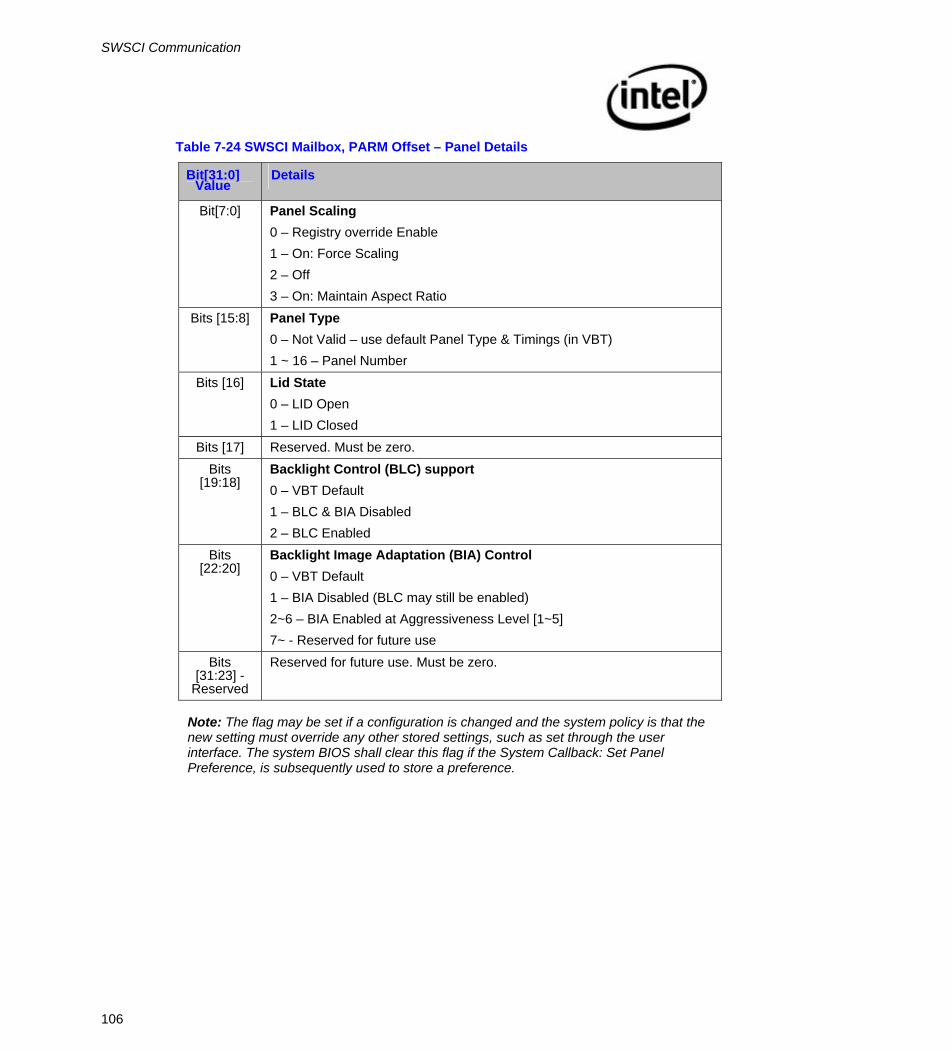
SWSCI Communication
106
Table 7-24 SWSCI Mailbox, PARM Offset – Panel Details
Bit[31:0] Value
Details
Bit[7:0] Panel Scaling 0 – Registry override Enable 1 – On: Force Scaling 2 – Off 3 – On: Maintain Aspect Ratio
Bits [15:8] Panel Type 0 – Not Valid – use default Panel Type & Timings (in VBT) 1 ~ 16 – Panel Number
Bits [16] Lid State 0 – LID Open 1 – LID Closed
Bits [17] Reserved. Must be zero. Bits
[19:18] Backlight Control (BLC) support 0 – VBT Default 1 – BLC & BIA Disabled 2 – BLC Enabled
Bits [22:20]
Backlight Image Adaptation (BIA) Control 0 – VBT Default 1 – BIA Disabled (BLC may still be enabled) 2~6 – BIA Enabled at Aggressiveness Level [1~5] 7~ - Reserved for future use
Bits [31:23] -
Reserved
Reserved for future use. Must be zero.
Note: The flag may be set if a configuration is changed and the system policy is that the new setting must override any other stored settings, such as set through the user interface. The system BIOS shall clear this flag if the System Callback: Set Panel Preference, is subsequently used to store a preference.
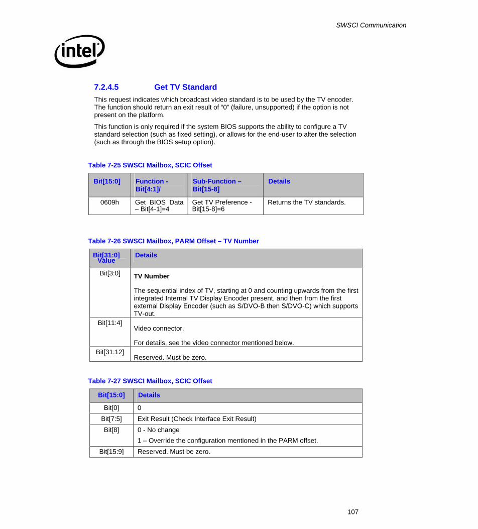
SWSCI Communication
107
7.2.4.5 Get TV Standard This request indicates which broadcast video standard is to be used by the TV encoder. The function should return an exit result of “0” (failure, unsupported) if the option is not present on the platform.
This function is only required if the system BIOS supports the ability to configure a TV standard selection (such as fixed setting), or allows for the end-user to alter the selection (such as through the BIOS setup option).
Table 7-25 SWSCI Mailbox, SCIC Offset
Bit[15:0] Function - Bit[4:1]/
Sub-Function – Bit[15-8]
Details
0609h Get BIOS Data – Bit[4-1]=4
Get TV Preference -Bit[15-8]=6
Returns the TV standards.
Table 7-26 SWSCI Mailbox, PARM Offset – TV Number
Bit[31:0] Value
Details
Bit[3:0] TV Number
The sequential index of TV, starting at 0 and counting upwards from the first integrated Internal TV Display Encoder present, and then from the first external Display Encoder (such as S/DVO-B then S/DVO-C) which supports TV-out.
Bit[11:4] Video connector.
For details, see the video connector mentioned below. Bit[31:12]
Reserved. Must be zero.
Table 7-27 SWSCI Mailbox, SCIC Offset
Bit[15:0] Details
Bit[0] 0 Bit[7:5] Exit Result (Check Interface Exit Result) Bit[8] 0 - No change
1 – Override the configuration mentioned in the PARM offset. Bit[15:9] Reserved. Must be zero.
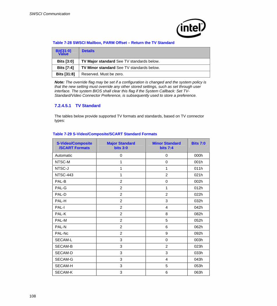
SWSCI Communication
108
Table 7-28 SWSCI Mailbox, PARM Offset – Return the TV Standard
Bit[31:0] Value
Details
Bits [3:0] TV Major standard See TV standards below. Bits [7:4] TV Minor standard See TV standards below.
Bits [31:8] Reserved. Must be zero.
Note: The override flag may be set if a configuration is changed and the system policy is that the new setting must override any other stored settings, such as set through user interface. The system BIOS shall clear this flag if the System Callback: Set TV-Standard/Video Connector Preference, is subsequently used to store a preference.
7.2.4.5.1 TV Standard
The tables below provide supported TV formats and standards, based on TV connector types:
Table 7-29 S-Video/Composite/SCART Standard Formats
S-Video/Composite /SCART Formats
Major Standard bits 3:0
Minor Standard bits 7:4
Bits 7:0
Automatic 0 0 000h
NTSC-M 1 0 001h
NTSC-J 1 1 011h
NTSC-443 1 2 021h
PAL-B 2 0 002h
PAL-G 2 1 012h
PAL-D 2 2 022h
PAL-H 2 3 032h
PAL-I 2 4 042h
PAL-K 2 8 082h
PAL-M 2 5 052h
PAL-N 2 6 062h
PAL-Nc 2 9 092h
SECAM-L 3 0 003h
SECAM-B 3 2 023h
SECAM-D 3 3 033h
SECAM-G 3 4 043h
SECAM-H 3 5 053h
SECAM-K 3 6 063h

SWSCI Communication
109
Table 7-30 Component/D-connector Standard Formats
Component/D-connector Formats
Major Standard bits 3:0
Minor Standard bits 7:4
Bits 7:0
SMPTE240M 1080i59 4 6 064h
SMPTE240M 1080i60 4 7 074h
BT1358_31 576p@50Hz 5 D 0D5h
BT6564_33576i@50Hz 5 5 055h
SMPTE295M 1080i50 7 5 057h
SMPTE295M 1080p50 7 D 0D7h
SMPTE296M 720p59 8 E 0E8h
SMPTE296M 720p60 8 F 0F8h
SMPTE296M 720p50 8 D 0D8h
HDTV_STD_CEA_7702_480p60 9 E 0E9h
HDTV_STD_CEA_7702_480p59 9 F 0F9h
HDTV_STD_CEA_7703_720p60 C E 0ECh
HDTV_STD_CEA_7703_720p59 C F 0FCh
HDTV_STD_CEA_7703_1080p60 D E 0EDh
HDTV_STD_CEA_7703_1080p59 D F 0FDh
HDTV_STD_CEA_7703_1080i60 E E 0EEh
HDTV_STD_CEA_7703_1080i59 E F 0FEh
HDTV_STD_CEA_7702_480i60 A 7 07Ah
HDTV_STD_CEA_7702_480i59 A 8 08Ah

SWSCI Communication
110
7.2.4.5.2 Video Connector
The video connector field indicates the type of connector attached to the specified TV encoder (TV number):
Table 7-31 Video Connector
Video Connector
TV Standard Table
Meaning
00h 1 Automatic (such as determined by registry, codec jumper/strap)
01h 1 Composite (such as RCA jack)
02h 2 Component (such as YPrPb/D-Connector)
03h 1 Both Composite & RGB
04h 1 S-video
05h 1 SCART with Composite Only
06h 2 SCART with Composite & RGB
07h 1 SCART with Composite & S-video
40h 2 SMPTE253_Component RGB (RGB-H/V)
7.2.4.6 Get Internal Graphics Settings
Assuming GMCH internal graphics is enabled (meaning device #2 is present) this field will return the current configuration information.
Note: The speed setting may differ from the value fused into the product. Typically it will be less than the originally intended setting.
Input:
Table 7-32 SWSCI Mailbox, SCIC Offset
Bit[15:0] Function - Bit[4:1]/
Sub-Function – Bit[15-8] Details
0709h Get BIOS Data – Bit[4-1]=4
Get internal graphics settings -Bit[15-8]=7
Returns the internal graphic setting.
SWSCI Mailbox, PARM offset – Initialized to zero by client

SWSCI Communication
111
Table 7-33 SWSCI Mailbox, SCIC Offset
Bit[15:0] Details
Bit[0] 0 Bit[7:5] Exit result (Check Interface Exit Result) Bit[8] 0 – No change
1 – Override the configuration mentioned in the PARM offset. Bit[15:9] Reserved. Must be zero.
Table 7-34 SWSCI Mailbox, PARM Offset – GMCH Configuration
Bit[31:0] Value
Details
Bit [0] GMCH VGA Mode 0 = Non-VGA 1 = VGA
Bit [1] FN, Device #2 should use 1 or 2 functions 0 = 1 Function (Single or Multi-Head) 1 = 2 Functions (Multi-Function)
Bit [2] Memory Type 0 – Pre-Allocated Memory 1 – Local Memory
Bit [3] SR/RD RAM Local memory self refresh 0 – Not Supported 1 – Self Refresh supported in power state S3,D3-Cold.
Bit [4] GMCH S3 State 0 = D3-Cold (default) 1 = D3-Hot
Bit[7:5] Pre-Allocated Graphics Memory Row 0 – Not Supported. UnKnown 1 – Row#0 3 – Row#1 5 – Row#2 7 – Row#3
Bit [10:8] Reserved. Bit [31:21] Current Graphics Core Speed (in MHz)
When multiple speeds are supported by the GMCH, this field will be the “Core-Clock High” speed.
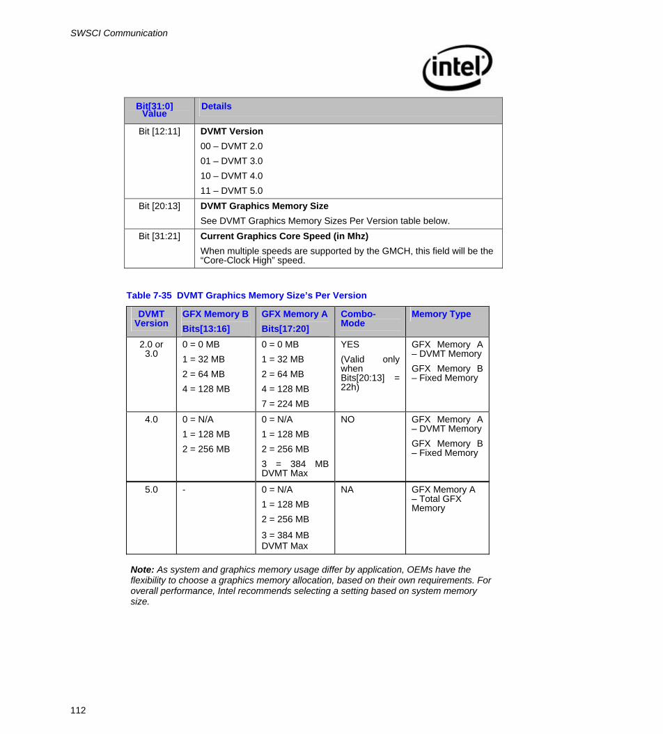
SWSCI Communication
112
Bit[31:0] Value
Details
Bit [12:11] DVMT Version 00 – DVMT 2.0 01 – DVMT 3.0 10 – DVMT 4.0 11 – DVMT 5.0
Bit [20:13] DVMT Graphics Memory Size See DVMT Graphics Memory Sizes Per Version table below.
Bit [31:21] Current Graphics Core Speed (in Mhz) When multiple speeds are supported by the GMCH, this field will be the “Core-Clock High” speed.
Table 7-35 DVMT Graphics Memory Size’s Per Version
DVMT Version
GFX Memory B Bits[13:16]
GFX Memory A Bits[17:20]
Combo-Mode
Memory Type
2.0 or 3.0
0 = 0 MB 1 = 32 MB 2 = 64 MB 4 = 128 MB
0 = 0 MB 1 = 32 MB 2 = 64 MB 4 = 128 MB 7 = 224 MB
YES (Valid only when Bits[20:13] = 22h)
GFX Memory A – DVMT Memory GFX Memory B – Fixed Memory
4.0 0 = N/A 1 = 128 MB 2 = 256 MB
0 = N/A 1 = 128 MB 2 = 256 MB 3 = 384 MB DVMT Max
NO GFX Memory A – DVMT Memory GFX Memory B – Fixed Memory
5.0 - 0 = N/A 1 = 128 MB 2 = 256 MB
3 = 384 MB DVMT Max
NA GFX Memory A – Total GFX Memory
Note: As system and graphics memory usage differ by application, OEMs have the flexibility to choose a graphics memory allocation, based on their own requirements. For overall performance, Intel recommends selecting a setting based on system memory size.
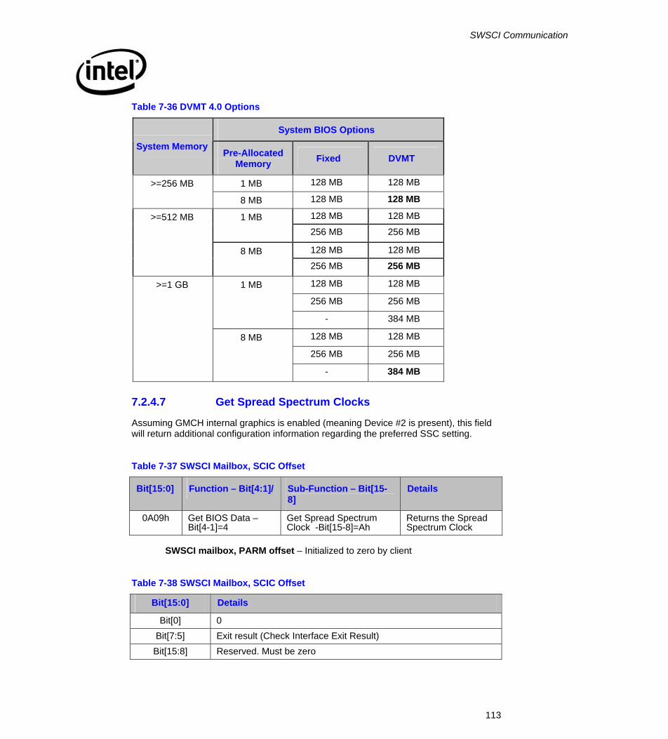
SWSCI Communication
113
Table 7-36 DVMT 4.0 Options
System BIOS Options
System Memory Pre-Allocated
Memory Fixed DVMT
1 MB 128 MB 128 MB >=256 MB
8 MB 128 MB 128 MB
128 MB 128 MB 1 MB
256 MB 256 MB
128 MB 128 MB
>=512 MB
8 MB 256 MB 256 MB
128 MB 128 MB
256 MB 256 MB
1 MB
- 384 MB
128 MB 128 MB
256 MB 256 MB
>=1 GB
8 MB
- 384 MB
7.2.4.7 Get Spread Spectrum Clocks
Assuming GMCH internal graphics is enabled (meaning Device #2 is present), this field will return additional configuration information regarding the preferred SSC setting.
Table 7-37 SWSCI Mailbox, SCIC Offset
Bit[15:0] Function – Bit[4:1]/ Sub-Function – Bit[15-8]
Details
0A09h Get BIOS Data – Bit[4-1]=4
Get Spread Spectrum Clock -Bit[15-8]=Ah
Returns the Spread Spectrum Clock
SWSCI mailbox, PARM offset – Initialized to zero by client
Table 7-38 SWSCI Mailbox, SCIC Offset
Bit[15:0] Details
Bit[0] 0 Bit[7:5] Exit result (Check Interface Exit Result) Bit[15:8] Reserved. Must be zero

SWSCI Communication
114
Table 7-39 SWSCI Mailbox, PARM Offset – Spread Spectrum Clock
Bit[31:0] Value
Details
Bit [0] SSC enabled 0 – SSC disabled 1 – SSC enabled
Bit [2:1] SSC Frequency 0 – Auto configuration. Use VBT or default settings 1 – SSC-Clock1 2 – SSC-Clock2 3 – SSC-Clock3
Bit [31:3] Reserved. Must be zero.
7.2.4.8 Supported Callbacks
This function can be called to discover which callbacks are supported. This does not mean the callback is requested – clients should use the GetBIOSData Requested System Callbacks function to discover that information.
Note: This function is itself new and may return an error code if unimplemented, such as on an older platform. This function shall only return success if the return value accurately lists supported callbacks.
Table 7-40 SWSCI Mailbox, SCIC Offset
Bit[15:0] Function - Bit[4:1]/ Sub-Function – Bit[15-8]
Details
000Dh System BIOS Callbacks – Bit[4-1]=6
Supported Callbacks -Bit[15-8]=0
Provides the supported callbacks.
SWSCI Mailbox, PARM offset - initialized to zero by the client.

SWSCI Communication
115
Table 7-41 SWSCI Mailbox, SCIC Offset
Bit[15:0] Details
Bit[0] 0 Bit[7:5] Exit Result (Check Interface Exit Result)
Bit[15:8] Reserved
Table 7-42 SWSCI Mailbox, PARM Offset – Bit Mask of Requested Callbacks
Bit[31:0] Value
Details
Bit [0] BIOS Post Completion Notification
Bit [1] Reserved
Bit [2] Pre-Hires Set Mode
Call before setting a new mode
Bit [3] Post-Hires Set Mode
Call after setting a new mode
Bit [4] Display Switch
Called when a display switch transition is occurring
Bit [5] Set TV Format
Set NTSC, PAL, SECAM or Other Setup option (Non-Volatile)
Bit [6] Adapter Power State
Called for Adapter PCI PM State Transition: Dx to D0 or D0 to Dx
Bit [7] Display Power State
Called for VESA VBE/PM
Bit [8] Set Boot Display
Sets the BIOS Setup-option (Non-Volatile) affecting boot-time Display preference
Bit [9] Set Panel Details
Sets the BIOS Setup-option (Non-Volatile) affecting boot-time Panel preference
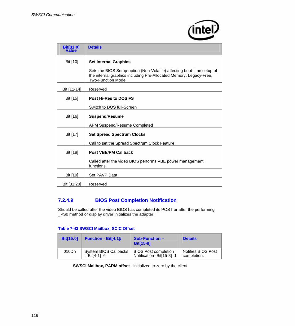
SWSCI Communication
116
Bit[31:0] Value
Details
Bit [10] Set Internal Graphics
Sets the BIOS Setup-option (Non-Volatile) affecting boot-time setup of the internal graphics including Pre-Allocated Memory, Legacy-Free, Two-Function Mode
Bit [11-14] Reserved
Bit [15] Post Hi-Res to DOS FS
Switch to DOS full-Screen
Bit [16] Suspend/Resume
APM Suspend/Resume Completed
Bit [17] Set Spread Spectrum Clocks
Call to set the Spread Spectrum Clock Feature
Bit [18] Post VBE/PM Callback
Called after the video BIOS performs VBE power management functions
Bit [19] Set PAVP Data
Bit [31:20] Reserved
7.2.4.9 BIOS Post Completion Notification
Should be called after the video BIOS has completed its POST or after the performing _PS0 method or display driver initializes the adapter.
Table 7-43 SWSCI Mailbox, SCIC Offset
Bit[15:0] Function - Bit[4:1]/ Sub-Function – Bit[15-8]
Details
010Dh System BIOS Callbacks – Bit[4-1]=6
BIOS Post completion Notification -Bit[15-8]=1
Notifies BIOS Post completion.
SWSCI Mailbox, PARM offset - initialized to zero by the client.
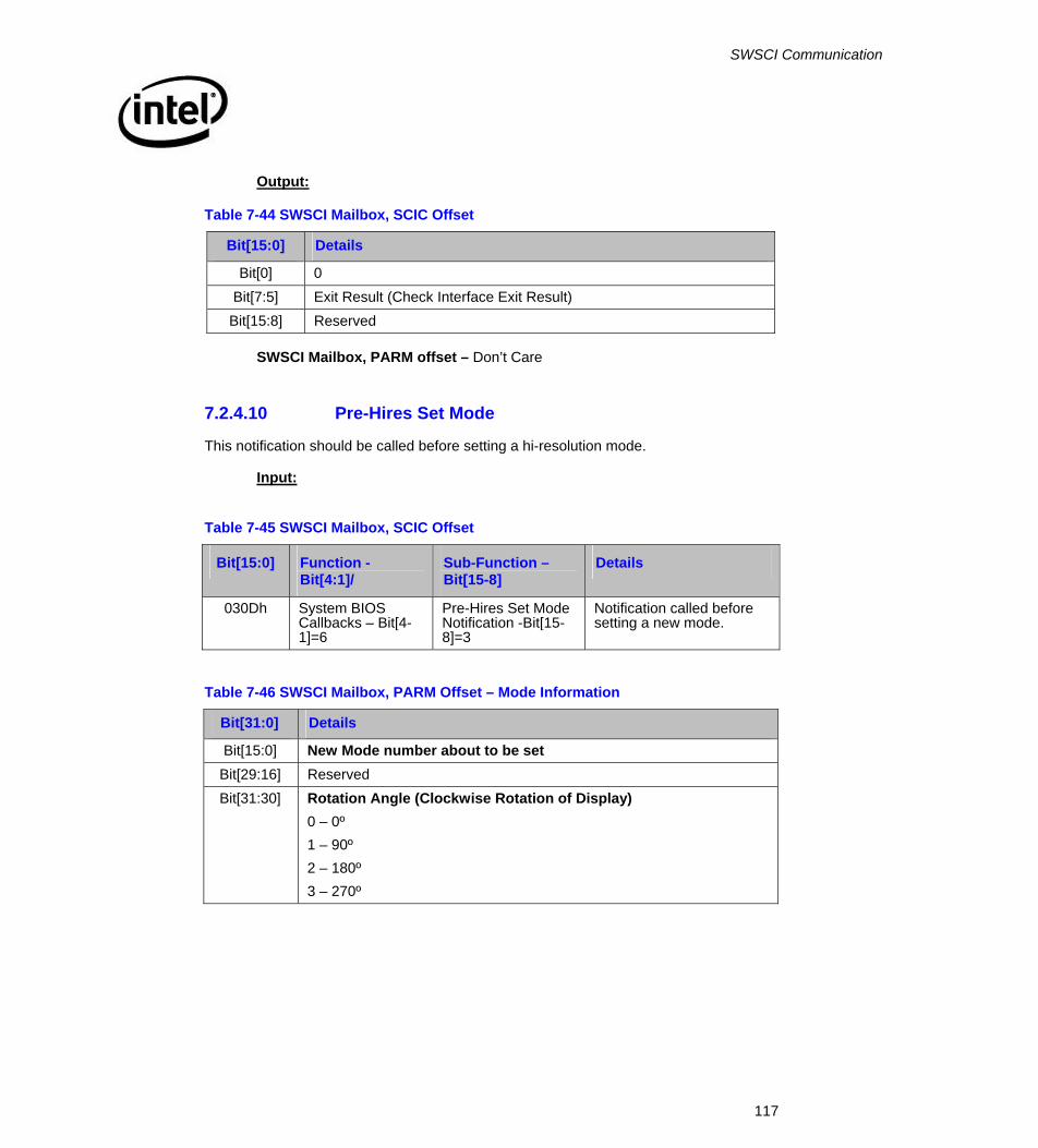
SWSCI Communication
117
Output:
Table 7-44 SWSCI Mailbox, SCIC Offset
Bit[15:0] Details
Bit[0] 0 Bit[7:5] Exit Result (Check Interface Exit Result) Bit[15:8] Reserved
SWSCI Mailbox, PARM offset – Don’t Care
7.2.4.10 Pre-Hires Set Mode
This notification should be called before setting a hi-resolution mode.
Input:
Table 7-45 SWSCI Mailbox, SCIC Offset
Bit[15:0] Function - Bit[4:1]/
Sub-Function – Bit[15-8]
Details
030Dh System BIOS Callbacks – Bit[4-1]=6
Pre-Hires Set Mode Notification -Bit[15-8]=3
Notification called before setting a new mode.
Table 7-46 SWSCI Mailbox, PARM Offset – Mode Information
Bit[31:0] Details
Bit[15:0] New Mode number about to be set Bit[29:16] Reserved Bit[31:30] Rotation Angle (Clockwise Rotation of Display)
0 – 0º 1 – 90º 2 – 180º 3 – 270º

SWSCI Communication
118
Table 7-47 SWSCI Mailbox, SCIC Offset
Bit[15:0] Details
Bit[0] 0 Bit[7:5] Exit Result (Check Interface Exit Result) Bit[15:8] Reserved
SWSCI Mailbox, PARM offset – Don’t Care
7.2.4.11 Post-Hires Set Mode
This notification should be called after setting a hi-resolution mode.
Input:
Table 7-48 SWSCI Mailbox, SCIC Offset
Bit[15:0] Function - Bit[4:1] Sub-Function – Bit[15-8]
Details
040Dh System BIOS Callbacks – Bit[4-1]=6
Post-Hires Set Mode Notification -Bit[15-8]=3
Notification called after setting a new mode.
Table 7-49 SWSCI Mailbox, PARM Offset – Mode Information
Bit[31:0] Details
Bit[15:0] New Mode number about to be set Bit[29:16] Mode Bit Definition
Text Mode Bit[23:16] – Number of character columns Bit[29:24] – Active Display Page
Graphics Mode Bit[29:16] – Reserved. Must be zero. Bit[31:30] Rotation Angle (Clockwise Rotation of Display)
0 – 0º 1 – 90º 2 – 180º 3 – 270º
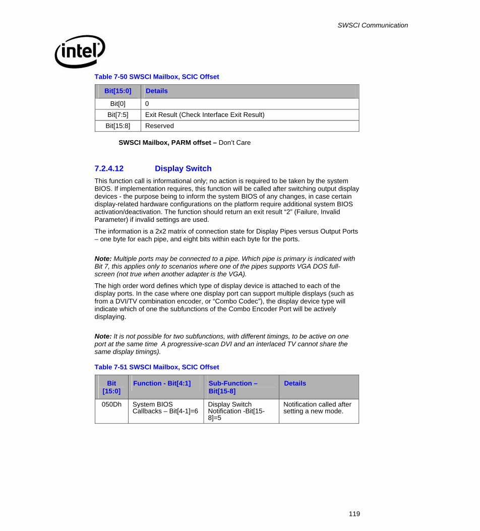
SWSCI Communication
119
Table 7-50 SWSCI Mailbox, SCIC Offset
Bit[15:0] Details
Bit[0] 0 Bit[7:5] Exit Result (Check Interface Exit Result)
Bit[15:8] Reserved
SWSCI Mailbox, PARM offset – Don’t Care
7.2.4.12 Display Switch This function call is informational only; no action is required to be taken by the system BIOS. If implementation requires, this function will be called after switching output display devices - the purpose being to inform the system BIOS of any changes, in case certain display-related hardware configurations on the platform require additional system BIOS activation/deactivation. The function should return an exit result “2” (Failure, Invalid Parameter) if invalid settings are used.
The information is a 2x2 matrix of connection state for Display Pipes versus Output Ports – one byte for each pipe, and eight bits within each byte for the ports.
Note: Multiple ports may be connected to a pipe. Which pipe is primary is indicated with Bit 7, this applies only to scenarios where one of the pipes supports VGA DOS full-screen (not true when another adapter is the VGA).
The high order word defines which type of display device is attached to each of the display ports. In the case where one display port can support multiple displays (such as from a DVI/TV combination encoder, or “Combo Codec”), the display device type will indicate which of one the subfunctions of the Combo Encoder Port will be actively displaying.
Note: It is not possible for two subfunctions, with different timings, to be active on one port at the same time A progressive-scan DVI and an interlaced TV cannot share the same display timings).
Table 7-51 SWSCI Mailbox, SCIC Offset
Bit [15:0]
Function - Bit[4:1] Sub-Function – Bit[15-8]
Details
050Dh System BIOS Callbacks – Bit[4-1]=6
Display Switch Notification -Bit[15-8]=5
Notification called after setting a new mode.
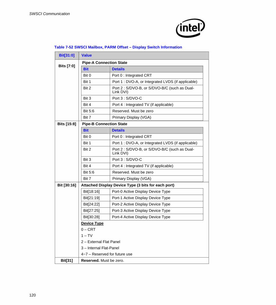
SWSCI Communication
120
Table 7-52 SWSCI Mailbox, PARM Offset – Display Switch Information
Bit[31:0] Value
Bits [7:0] Pipe-A Connection State
Bit Details Bit 0 Port 0 : Integrated CRT Bit 1 Port 1 : DVO-A, or Integrated LVDS (if applicable) Bit 2 Port 2 : S/DVO-B, or S/DVO-B/C (such as Dual-
Link DVI) Bit 3 Port 3 : S/DVO-C Bit 4 Port 4 : Integrated TV (if applicable) Bit 5:6 Reserved. Must be zero Bit 7 Primary Display (VGA)
Bits [15:8] Pipe-B Connection State Bit Details Bit 0 Port 0 : Integrated CRT Bit 1 Port 1 : DVO-A, or Integrated LVDS (if applicable) Bit 2 Port 2 : S/DVO-B, or S/DVO-B/C (such as Dual-
Link DVI) Bit 3 Port 3 : S/DVO-C Bit 4 Port 4 : Integrated TV (if applicable) Bit 5:6 Reserved. Must be zero Bit 7 Primary Display (VGA)
Bit [30:16] Attached Display Device Type (3 bits for each port) Bit[18:16] Port-0 Active Display Device Type Bit[21:19] Port-1 Active Display Device Type Bit[24:22] Port-2 Active Display Device Type Bit[27:25] Port-3 Active Display Device Type Bit[30:28] Port-4 Active Display Device Type
Device Type 0 – CRT 1 – TV 2 – External Flat Panel 3 – Internal Flat-Panel 4~7 – Reserved for future use
Bit[31] Reserved. Must be zero.
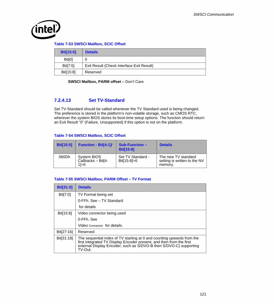
SWSCI Communication
121
Table 7-53 SWSCI Mailbox, SCIC Offset
Bit[15:0] Details
Bit[0] 0 Bit[7:5] Exit Result (Check Interface Exit Result) Bit[15:8] Reserved
SWSCI Mailbox, PARM offset – Don’t Care
7.2.4.13 Set TV-Standard
Set TV-Standard should be called whenever the TV Standard used is being changed. The preference is stored in the platform’s non-volatile storage, such as CMOS RTC, wherever the system BIOS stores its boot-time setup options. The function should return an Exit Result “0” (Failure, Unsupported) if this option is not on the platform.
Table 7-54 SWSCI Mailbox, SCIC Offset
Bit[15:0] Function - Bit[4:1]/ Sub-Function – Bit[15-8]
Details
060Dh System BIOS Callbacks – Bit[4-1]=6
Set TV Standard -Bit[15-8]=6
The new TV standard setting is written to the NV memory.
Table 7-55 SWSCI Mailbox, PARM Offset – TV Format
Bit[31:0] Details
Bit[7:0] TV Format being set 0-FFh. See – TV Standard for details
Bit[15:8] Video connector being used 0-FFh. See Video Connector for details.
Bit[27:16] Reserved Bit[31:18] The sequential index of TV starting at 0 and counting upwards from the
first integrated TV Display Encoder present, and then from the first external Display Encoder, such as S/DVO-B then S/DVO-C) supporting TV-Out.

SWSCI Communication
122
Table 7-56 SWSCI Mailbox, SCIC Offset – TV Format
Bit[15:0] Details
Bit[0] 0 Bit[7:5] Exit Result (Check Interface Exit Result)
Bit[15:8] Reserved
SWSCI Mailbox, PARM offset – Don’t Care
7.2.4.14 Adapter Power State Notification
Adapter Power State Notification should be called before the adapter (implies child devices and displays are already in a lower power state) is about to be placed in a lower power State (D0 -> Dx), and after the adapter is placed in a higher power state (such as (Dx -> D0) such as by APM/ACPI).
Table 7-57 SWSCI Mailbox, SCIC Offset
Bit[15:0] Function - Bit[4:1]/ Sub-Function – Bit[15-8]
Details
070Dh System BIOS Callbacks – Bit[4-1]=6
Set Adapter Power State Notification -Bit[15-8]=7
Notification called after setting the adapter to the new power state.
Table 7-58 SWSCI Mailbox, PARM Offset – Adapter Power State
Bit[31:0] Details
Bit[7:0] Power State 00h = D0 01h = D1 02h = D2 04h = D3 (Cold or Hot) 08h = D4 (Hibernate Notification)
Bit[31:8] Reserved
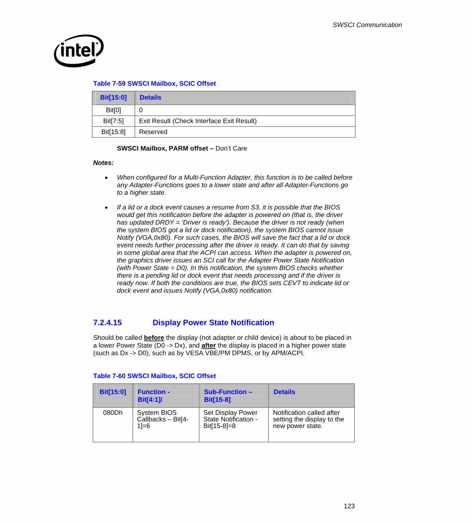
SWSCI Communication
123
Table 7-59 SWSCI Mailbox, SCIC Offset
Bit[15:0] Details
Bit[0] 0 Bit[7:5] Exit Result (Check Interface Exit Result) Bit[15:8] Reserved
SWSCI Mailbox, PARM offset – Don’t Care
Notes:
• When configured for a Multi-Function Adapter, this function is to be called before any Adapter-Functions goes to a lower state and after all Adapter-Functions go to a higher state.
• If a lid or a dock event causes a resume from S3, it is possible that the BIOS would get this notification before the adapter is powered on (that is, the driver has updated DRDY = ‘Driver is ready’). Because the driver is not ready (when the system BIOS got a lid or dock notification), the system BIOS cannot issue Notify (VGA,0x80). For such cases, the BIOS will save the fact that a lid or dock event needs further processing after the driver is ready. It can do that by saving in some global area that the ACPI can access. When the adapter is powered on, the graphics driver issues an SCI call for the Adapter Power State Notification (with Power State = D0). In this notification, the system BIOS checks whether there is a pending lid or dock event that needs processing and if the driver is ready now. If both the conditions are true, the BIOS sets CEVT to indicate lid or dock event and issues Notify (VGA,0x80) notification.
7.2.4.15 Display Power State Notification
Should be called before the display (not adapter or child device) is about to be placed in a lower Power State (D0 -> Dx), and after the display is placed in a higher power state (such as Dx -> D0), such as by VESA VBE/PM DPMS, or by APM/ACPI.
Table 7-60 SWSCI Mailbox, SCIC Offset
Bit[15:0] Function - Bit[4:1]/
Sub-Function – Bit[15-8]
Details
080Dh System BIOS Callbacks – Bit[4-1]=6
Set Display Power State Notification -Bit[15-8]=8
Notification called after setting the display to the new power state.

SWSCI Communication
124
Table 7-61 SWSCI Mailbox, PARM Offset – Display Power State
Bit[31:0] Details
Bit[7:0] 00h = Port-0 : Integrated CRT 01h = Port-1 : DVO-A or Integrated LVDS 02h = Port-2 : S/DVO-B or S/DVO-B/C (such as Dual-Link DVI) 04h = Port-3 : S/DVO-C 08h = Port-4 : Integrated TV
Bit[15:8] 00h = On 01h = Standby 02h = Suspend 04h = Off 08h = Reduced on
Bit [30:16] Port Display Device Type (3 bits for each port) Bit[18:16] Port-0 Display Device Type Bit[21:19] Port-1 Display Device Type Bit[24:22] Port-2 Display Device Type Bit[27:25] Port-3 Display Device Type Bit[30:28] Port-4 Display Device Type
Device Type 0 – CRT 1 – TV 2 – External Flat Panel 3 – Internal Flat-Panel 4~7 – Reserved for future use
Bit [31] Reserved
Table 7-62 SWSCI Mailbox, SCIC Offset
Bit[15:0] Details
Bit[0] 0 Bit[7:5] Exit Result (Check Interface Exit Result) Bit[15:8] Reserved
SWSCI Mailbox, PARM offset – Don’t Care
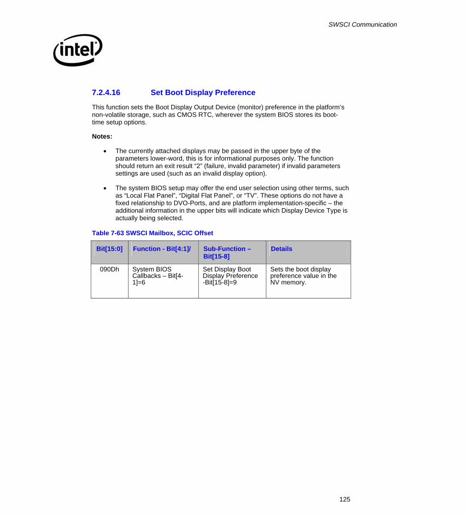
SWSCI Communication
125
7.2.4.16 Set Boot Display Preference
This function sets the Boot Display Output Device (monitor) preference in the platform’s non-volatile storage, such as CMOS RTC, wherever the system BIOS stores its boot-time setup options.
Notes:
• The currently attached displays may be passed in the upper byte of the parameters lower-word, this is for informational purposes only. The function should return an exit result “2” (failure, invalid parameter) if invalid parameters settings are used (such as an invalid display option).
• The system BIOS setup may offer the end user selection using other terms, such as “Local Flat Panel”, “Digital Flat Panel”, or “TV”. These options do not have a fixed relationship to DVO-Ports, and are platform implementation-specific – the additional information in the upper bits will indicate which Display Device Type is actually being selected.
Table 7-63 SWSCI Mailbox, SCIC Offset
Bit[15:0] Function - Bit[4:1]/ Sub-Function – Bit[15-8]
Details
090Dh System BIOS Callbacks – Bit[4-1]=6
Set Display Boot Display Preference -Bit[15-8]=9
Sets the boot display preference value in the NV memory.
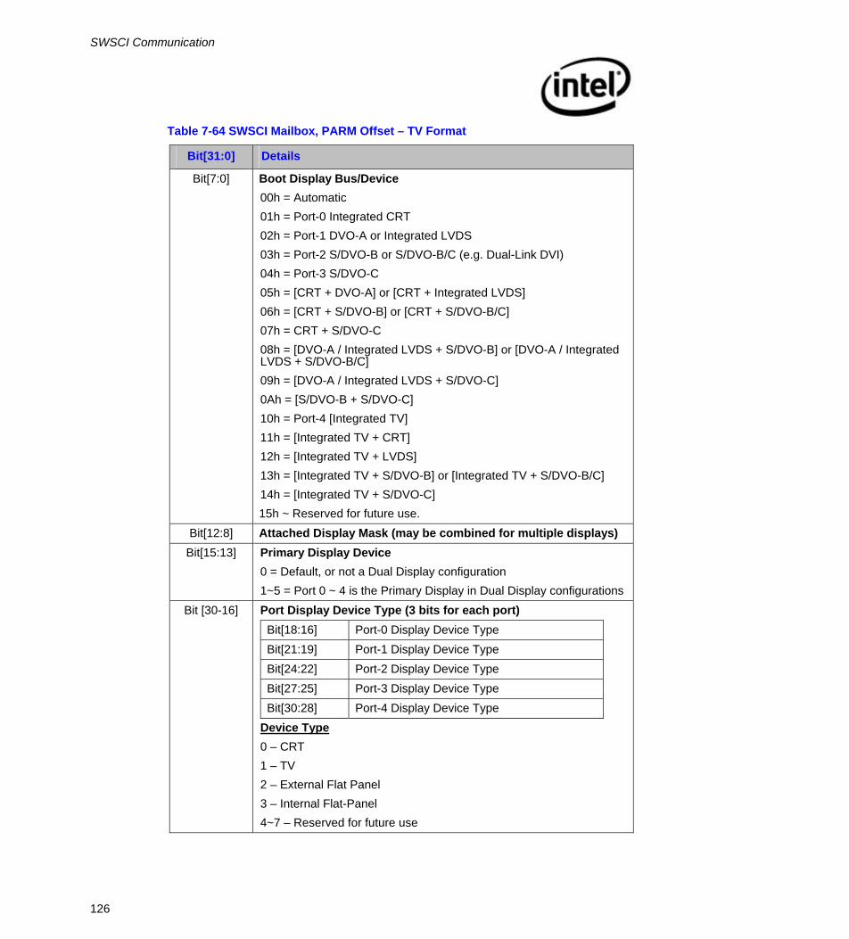
SWSCI Communication
126
Table 7-64 SWSCI Mailbox, PARM Offset – TV Format
Bit[31:0] Details
Bit[7:0] Boot Display Bus/Device 00h = Automatic 01h = Port-0 Integrated CRT 02h = Port-1 DVO-A or Integrated LVDS 03h = Port-2 S/DVO-B or S/DVO-B/C (e.g. Dual-Link DVI) 04h = Port-3 S/DVO-C 05h = [CRT + DVO-A] or [CRT + Integrated LVDS] 06h = [CRT + S/DVO-B] or [CRT + S/DVO-B/C] 07h = CRT + S/DVO-C 08h = [DVO-A / Integrated LVDS + S/DVO-B] or [DVO-A / Integrated LVDS + S/DVO-B/C] 09h = [DVO-A / Integrated LVDS + S/DVO-C] 0Ah = [S/DVO-B + S/DVO-C] 10h = Port-4 [Integrated TV] 11h = [Integrated TV + CRT] 12h = [Integrated TV + LVDS] 13h = [Integrated TV + S/DVO-B] or [Integrated TV + S/DVO-B/C] 14h = [Integrated TV + S/DVO-C] 15h ~ Reserved for future use.
Bit[12:8] Attached Display Mask (may be combined for multiple displays) Bit[15:13] Primary Display Device
0 = Default, or not a Dual Display configuration 1~5 = Port 0 ~ 4 is the Primary Display in Dual Display configurations
Bit [30-16] Port Display Device Type (3 bits for each port) Bit[18:16] Port-0 Display Device Type Bit[21:19] Port-1 Display Device Type Bit[24:22] Port-2 Display Device Type Bit[27:25] Port-3 Display Device Type Bit[30:28] Port-4 Display Device Type
Device Type 0 – CRT 1 – TV 2 – External Flat Panel 3 – Internal Flat-Panel 4~7 – Reserved for future use

SWSCI Communication
127
Bit[31:0] Details
Bit [31] Extended Desktop Configuration 0 = Single Display or Dual-Display Twin/Clone 1 = Dual-Display Extended Desktop
Table 7-65 SWSCI Mailbox, SCIC Offset
Bit[15:0] Details
Bit[0] 0 Bit[7:5] Exit result (Check Interface Exit Result) Bit[15:8] Reserved
SWSCI Mailbox, PARM offset – Don’t care.
Note: If Dual-Link Mode is used then S/DVO-B will be indicated
7.2.4.17 Set Panel Preference
This function sets the Flat Panel Scaling preference in the platform’s non-volatile storage, such as CMOS RTC, wherever the system BIOS stores its boot-time setup options.
This function is optional, and is required only for platforms with an internal flat-panel, such as mobile notebooks or all-in-one desktops. The function should return an Exit Result of “0” (failure, unsupported), if not supported on the platform.
Table 7-66 SWSCI Mailbox, SCIC Offset
Bit[15:0] Function - Bit[4:1]/ Sub-Function – Bit[15-8]
Details
0A0Dh System BIOS Callbacks – Bit[4-1]=6
Set Panel Preference -Bit[15-8]=A
Sets the panel preference value in the NV memory.
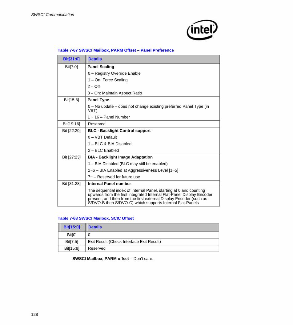
SWSCI Communication
128
Table 7-67 SWSCI Mailbox, PARM Offset – Panel Preference
Bit[31:0] Details
Bit[7:0] Panel Scaling 0 – Registry Override Enable 1 – On: Force Scaling 2 – Off 3 – On: Maintain Aspect Ratio
Bit[15:8] Panel Type 0 – No update – does not change existing preferred Panel Type (in VBT) 1 ~ 16 – Panel Number
Bit[19:16] Reserved Bit [22:20] BLC - Backlight Control support
0 – VBT Default 1 – BLC & BIA Disabled 2 – BLC Enabled
Bit [27:23] BIA - Backlight Image Adaptation 1 – BIA Disabled (BLC may still be enabled) 2~6 – BIA Enabled at Aggressiveness Level [1~5] 7~ – Reserved for future use
Bit [31:28] Internal Panel number The sequential index of Internal Panel, starting at 0 and counting
upwards from the first integrated Internal Flat-Panel Display Encoder present, and then from the first external Display Encoder (such as S/DVO-B then S/DVO-C) which supports Internal Flat-Panels
Table 7-68 SWSCI Mailbox, SCIC Offset
Bit[15:0] Details
Bit[0] 0 Bit[7:5] Exit Result (Check Interface Exit Result) Bit[15:8] Reserved
SWSCI Mailbox, PARM offset – Don’t care.

SWSCI Communication
129
7.2.4.18 Switch to Full-Screen
This function is provided to override the display selection when entering DOS full-screen. This call is made after the switch has completed.
This SCI notification is optional only if the platform does not support Hi-Res to Full Screen mode transition, or vice-versa. Otherwise, the system BIOS should implement both of these functions: Pre-Hires Set Mode and Post-Hires Set Mode.
Table 7-69 SWSCI Mailbox, SCIC Offset
Bit[15:0] Function - Bit[4:1]/ Sub-Function – Bit[15-8]
Details
100Dh System BIOS Callbacks – Bit[4-1]=6
Notify System BIOS on Switch to FSDOS-Bit[15-8]=10h
Notifies the system BIOS of any switch to the FSDOS.
Table 7-70 SWSCI Mailbox, PARM Offset – Internal Graphics Preference
Bit[31:0] Details
Bit[7:0] Switch 0 – Switched to DOS Full-Screen 1 – Switched to Native Hi-Res 2~ – Reserved
Bit[31:8] Reserved. Must be zero.
Table 7-71 SWSCI Mailbox, SCIC Offset
Bit[15:0] Details
Bit[0] 0 Bit[7:5] Exit Result (Check Interface Exit Result)
Bit[15:8] Reserved
SWSCI Mailbox, PARM offset – Don’t care.
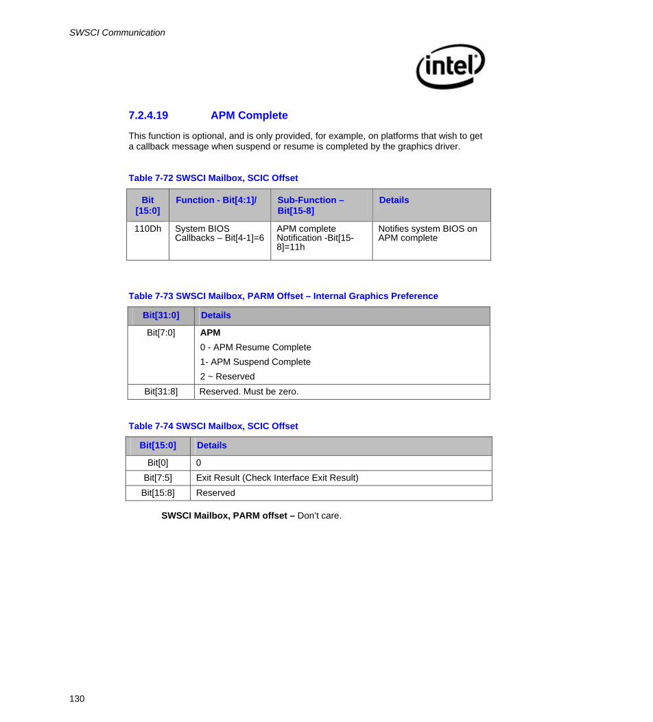
SWSCI Communication
130
7.2.4.19 APM Complete
This function is optional, and is only provided, for example, on platforms that wish to get a callback message when suspend or resume is completed by the graphics driver.
Table 7-72 SWSCI Mailbox, SCIC Offset
Bit [15:0]
Function - Bit[4:1]/ Sub-Function – Bit[15-8]
Details
110Dh System BIOS Callbacks – Bit[4-1]=6
APM complete Notification -Bit[15-8]=11h
Notifies system BIOS on APM complete
Table 7-73 SWSCI Mailbox, PARM Offset – Internal Graphics Preference
Bit[31:0] Details
Bit[7:0] APM 0 - APM Resume Complete 1- APM Suspend Complete 2 ~ Reserved
Bit[31:8] Reserved. Must be zero.
Table 7-74 SWSCI Mailbox, SCIC Offset
Bit[15:0] Details
Bit[0] 0 Bit[7:5] Exit Result (Check Interface Exit Result)
Bit[15:8] Reserved
SWSCI Mailbox, PARM offset – Don’t care.
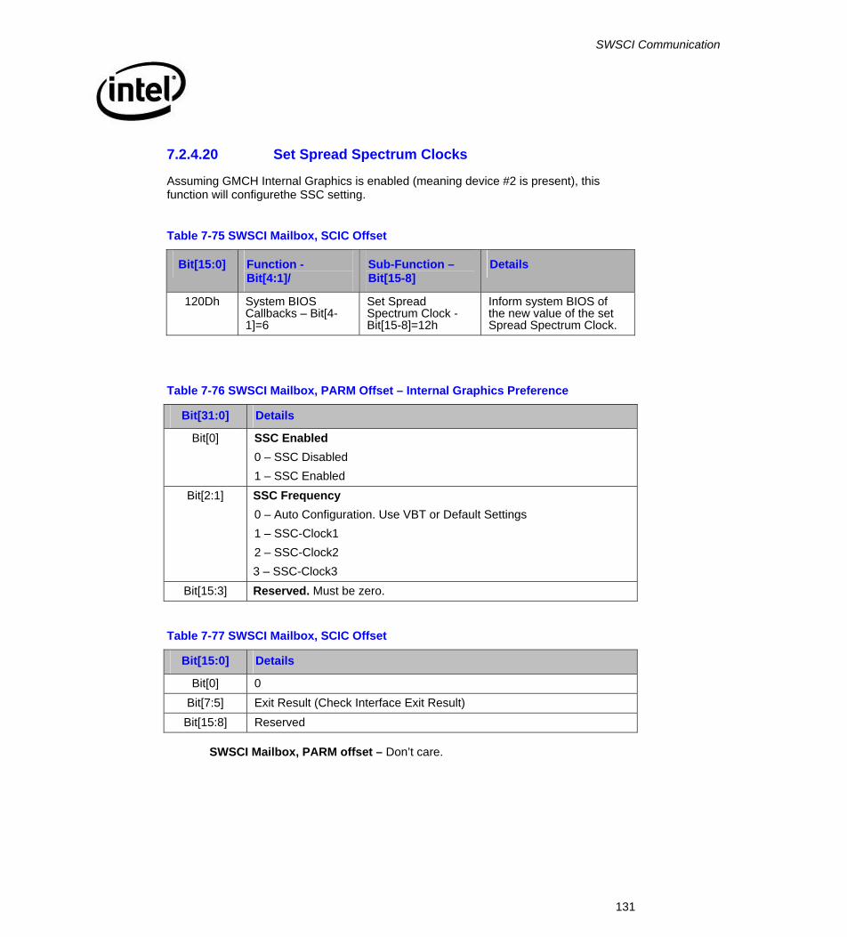
SWSCI Communication
131
7.2.4.20 Set Spread Spectrum Clocks
Assuming GMCH Internal Graphics is enabled (meaning device #2 is present), this function will configurethe SSC setting.
Table 7-75 SWSCI Mailbox, SCIC Offset
Bit[15:0] Function - Bit[4:1]/
Sub-Function – Bit[15-8]
Details
120Dh System BIOS Callbacks – Bit[4-1]=6
Set Spread Spectrum Clock -Bit[15-8]=12h
Inform system BIOS of the new value of the set Spread Spectrum Clock.
Table 7-76 SWSCI Mailbox, PARM Offset – Internal Graphics Preference
Bit[31:0] Details
Bit[0] SSC Enabled 0 – SSC Disabled 1 – SSC Enabled
Bit[2:1] SSC Frequency 0 – Auto Configuration. Use VBT or Default Settings 1 – SSC-Clock1 2 – SSC-Clock2 3 – SSC-Clock3
Bit[15:3] Reserved. Must be zero.
Table 7-77 SWSCI Mailbox, SCIC Offset
Bit[15:0] Details
Bit[0] 0 Bit[7:5] Exit Result (Check Interface Exit Result) Bit[15:8] Reserved
SWSCI Mailbox, PARM offset – Don’t care.
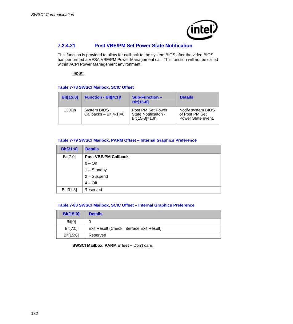
SWSCI Communication
132
7.2.4.21 Post VBE/PM Set Power State Notification
This function is provided to allow for callback to the system BIOS after the video BIOS has performed a VESA VBE/PM Power Management call. This function will not be called within ACPI Power Management environment.
Input:
Table 7-78 SWSCI Mailbox, SCIC Offset
Bit[15:0] Function - Bit[4:1]/ Sub-Function – Bit[15-8]
Details
130Dh System BIOS Callbacks – Bit[4-1]=6
Post PM Set Power State Notificaiton -Bit[15-8]=13h
Notify system BIOS of Post PM Set Power State event.
Table 7-79 SWSCI Mailbox, PARM Offset – Internal Graphics Preference
Bit[31:0] Details
Bit[7:0] Post VBE/PM Callback 0 – On 1 – Standby 2 – Suspend 4 – Off
Bit[31:8] Reserved
Table 7-80 SWSCI Mailbox, SCIC Offset – Internal Graphics Preference
Bit[15:0] Details
Bit[0] 0 Bit[7:5] Exit Result (Check Interface Exit Result) Bit[15:8] Reserved
SWSCI Mailbox, PARM offset – Don’t care.
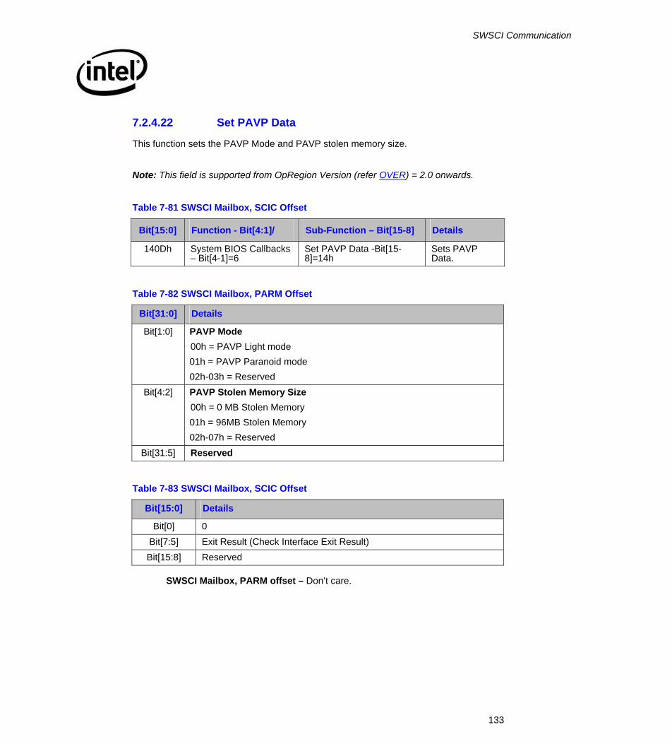
SWSCI Communication
133
7.2.4.22 Set PAVP Data
This function sets the PAVP Mode and PAVP stolen memory size.
Note: This field is supported from OpRegion Version (refer OVER) = 2.0 onwards.
Table 7-81 SWSCI Mailbox, SCIC Offset
Bit[15:0] Function - Bit[4:1]/ Sub-Function – Bit[15-8] Details
140Dh System BIOS Callbacks – Bit[4-1]=6
Set PAVP Data -Bit[15-8]=14h
Sets PAVP Data.
Table 7-82 SWSCI Mailbox, PARM Offset
Bit[31:0] Details
Bit[1:0] PAVP Mode 00h = PAVP Light mode 01h = PAVP Paranoid mode 02h-03h = Reserved
Bit[4:2] PAVP Stolen Memory Size 00h = 0 MB Stolen Memory 01h = 96MB Stolen Memory 02h-07h = Reserved
Bit[31:5] Reserved
Table 7-83 SWSCI Mailbox, SCIC Offset
Bit[15:0] Details
Bit[0] 0 Bit[7:5] Exit Result (Check Interface Exit Result)
Bit[15:8] Reserved
SWSCI Mailbox, PARM offset – Don’t care.
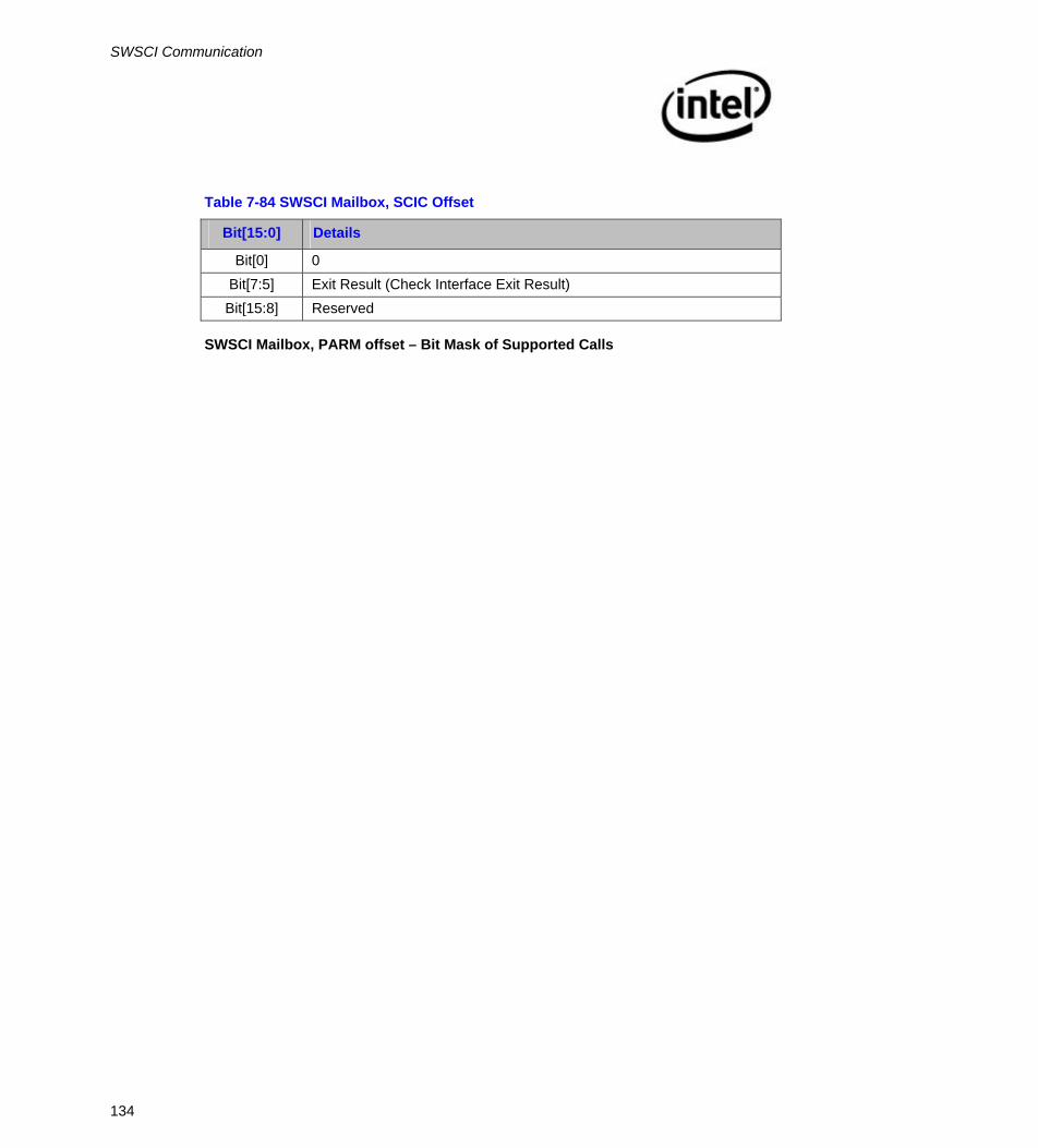
SWSCI Communication
134
Table 7-84 SWSCI Mailbox, SCIC Offset
Bit[15:0] Details
Bit[0] 0 Bit[7:5] Exit Result (Check Interface Exit Result) Bit[15:8] Reserved
SWSCI Mailbox, PARM offset – Bit Mask of Supported Calls


![[MS-RDPEGDI]: Remote Desktop Protocol: Graphics Device ... · Remote Desktop Protocol: Graphics Device Interface (GDI) Acceleration Extensions Intellectual Property Rights Notice](https://static.documents.pub/doc/80x56/5f288d906ae189393340920c/ms-rdpegdi-remote-desktop-protocol-graphics-device-remote-desktop-protocol.jpg)


