September 29, 2015 11:8 World Scientific Review Volume - 9.75in x 6.5in active˙meta page 1 Chapter 1 Active Metamaterials Michael D. Singh and Marek S. Wartak * Department of Physics and Computer Science, Wilfrid Laurier University, Waterloo, Ontario, Canada [email protected]† The outstanding properties of metamaterials open the door of opportunity for a number of exciting practical applications. Fascinating applications such as: per- fect lenses that break the diffraction limit of conventional lenses, optical quantum storage, and invisibility cloaking. These dramatic new technological advance- ments are being severely hindered by the significant loss effects of metamaterials. Overcoming loss limitations is currently one of the most important topics in meta- materials research. Presented in the paper are loss reduction schemes regarding: the geometric shape of metamaterial components, parameter manipulation, and parametric amplification. Active gain is then discussed with experimental and theoretical approaches involving loss compensation of active metamaterials. Next, surface plasmons are introduced discussing the intriguing concepts of spasers and metamaterial lasing spasers. Finally, we move to the opposite direction and con- sider increasing losses in metamaterials to create near perfect metamaterial ab- sorbers that can find applications in the solar cell industry as well as other fields of science. 1. Introduction The properties exhibited by a substance which is found in nature is determined by the chemical elements and bonds that form the structure. By precisely arranging the elements of a structure, an artificial material can be created. This artificially engineered material, a material that is beyond a naturally occurring one, is known as a metamaterial (”meta” - Greek word for beyond). 1 Since a metamaterial is artificially produced and to the best of our knowledge cannot be found in nature, it exhibits exotic and potentially advantageous properties that we can utilize. The electromagnetic properties of any medium are determined by two funda- mental parameters: electric permittivity () and magnetic permeability (μ). The square-root of the product of the two parameters defines the refractive index of a material * Author footnote. † Affiliation footnote. 1
Transcript
September 29, 2015 11:8 World Scientific Review Volume - 9.75in x 6.5in active˙meta page 1
Chapter 1
Active Metamaterials
Michael D. Singh and Marek S. Wartak∗
Department of Physics and Computer Science,Wilfrid Laurier University, Waterloo, Ontario, Canada
The outstanding properties of metamaterials open the door of opportunity for anumber of exciting practical applications. Fascinating applications such as: per-fect lenses that break the diffraction limit of conventional lenses, optical quantumstorage, and invisibility cloaking. These dramatic new technological advance-ments are being severely hindered by the significant loss effects of metamaterials.Overcoming loss limitations is currently one of the most important topics in meta-materials research. Presented in the paper are loss reduction schemes regarding:the geometric shape of metamaterial components, parameter manipulation, andparametric amplification. Active gain is then discussed with experimental andtheoretical approaches involving loss compensation of active metamaterials. Next,surface plasmons are introduced discussing the intriguing concepts of spasers andmetamaterial lasing spasers. Finally, we move to the opposite direction and con-sider increasing losses in metamaterials to create near perfect metamaterial ab-sorbers that can find applications in the solar cell industry as well as other fieldsof science.
1. Introduction
The properties exhibited by a substance which is found in nature is determined by
the chemical elements and bonds that form the structure. By precisely arranging
the elements of a structure, an artificial material can be created. This artificially
engineered material, a material that is beyond a naturally occurring one, is known
as a metamaterial (”meta” - Greek word for beyond).1 Since a metamaterial is
artificially produced and to the best of our knowledge cannot be found in nature,
it exhibits exotic and potentially advantageous properties that we can utilize.
The electromagnetic properties of any medium are determined by two funda-
mental parameters: electric permittivity (ε) and magnetic permeability (µ). The
square-root of the product of the two parameters defines the refractive index of a
material
∗Author footnote.†Affiliation footnote.
1
September 29, 2015 11:8 World Scientific Review Volume - 9.75in x 6.5in active˙meta page 2
2 Michael D. Singh and Marek S. Wartak
n =√εµ (1)
A material simultaneously having negative electric permittivity and negative
magnetic permeability is a metamaterial. Since both ε and µ are negative, the
product of the two is a positive real number. Interestingly, this means that the
refractive index is a real negative number. To illustrate why the refractive index
becomes a negative number, see this simple example (for a more complete discussion,
see [2])
Let, ε = −1 and µ = −1
n =√εµ
n =√
(−1)(−1)
n =√
(−1)√
(−1)
n = i× in = −1
Thus, metamaterials are characterized by having a negative index of refraction,
and are often referred to as negative index materials.
In recent years the field of metamaterials has received remarkable attention
with the number of published papers growing exponentially. This is due to unusual
properties of such systems (see [3] for a recent review) and also important practical
applications like perfect lenses [4], invisibility cloaking [5], [6], slow light [7], and
enhanced optical nonlinearities [8]. Parallel to theoretical developments there has
been spectacular experimental progress [9].
The full exploitation of metamaterials suffers due to the existence of losses which
at present are orders of magnitude that are too large for practical applications and
are considered as an important factor limiting practical applications of metama-
terials. For example, detailed analytical studies show that losses limit the super-
resolution of a theoretical super-lens [10]. There was some controversy about the
possibilities of eliminating losses [11] but as shown by Webb and Thylen [12] it is
possible to completely eliminate losses in metamaterials.
In recent years there has been several reports [13], [14], [15] about possible com-
pensation of losses in metamaterials by introducing gain elements. For example, We-
gener et al [14] formulated a simple model where gain is represented by a fermionic
two-level system which is coupled via a local-field to a single bosonic resonance
representing the plasmonic resonance of metamaterial. Also recently, Fang et al
[15] described a model where gain system is modelled by generic four-level atomic
system. They conducted numerical analysis using FDTD technique. Two geome-
tries were considered. In the magnetic one, the gain material is introduced in the
gap region of the split-ring resonators (SRR). The system has a magnetic resonance
September 29, 2015 11:8 World Scientific Review Volume - 9.75in x 6.5in active˙meta page 3
Active Metamaterials 3
frequency at 100THz. Some other reports of the design and analysis of active
metamaterials are by Yuan et al [16] and Sivan et al [17].
2. Metamaterial Structures
The idea of left-handed materials was first introduced theoretically by Vesalgo in
his theoretical work [18], but it was not until Pendry et al [19] in 1999 when the
scientific world took notice. Their work demonstrated a practical way of fabricating
the once theoretical metamaterials by using a split-ring resonator structure. Since
then metamaterial research has been a highly popular and significant research area.
Currently the two most prominent metamaterial structures which effectively achieve
simultaneous negative electric permittivity and magnetic permeability are split-ring
resonator (SRR) structures and fishnet structures.20
2.1. Split-ring Resonator Structures
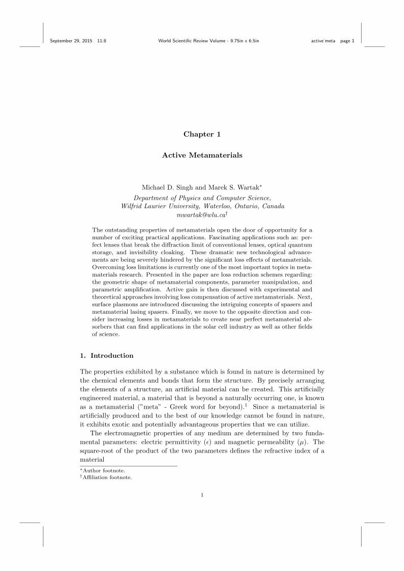
A split-ring resonator consists of a pair of concentric non-magnetic metallic rings,
with slit separations on opposite sides (see Fig. 1). One can generate a magnetic
resonance by inducing rotational currents within the SRR. As shown in [19], a
negative permeability can be realized in a periodic array of SRRs. A negative electric
permittivity can be achieved by using ultra-thin metallic wires, at all frequencies
below the plasma frequency.19 Thus a periodic array of SRRs consisting of non-
magnetic metallic nanowires can achieve simultaneous negative electric permittivity
and magnetic permeability, given the correct parameters, as shown in [21].
Fig. 1. A split-ring resonator structure.
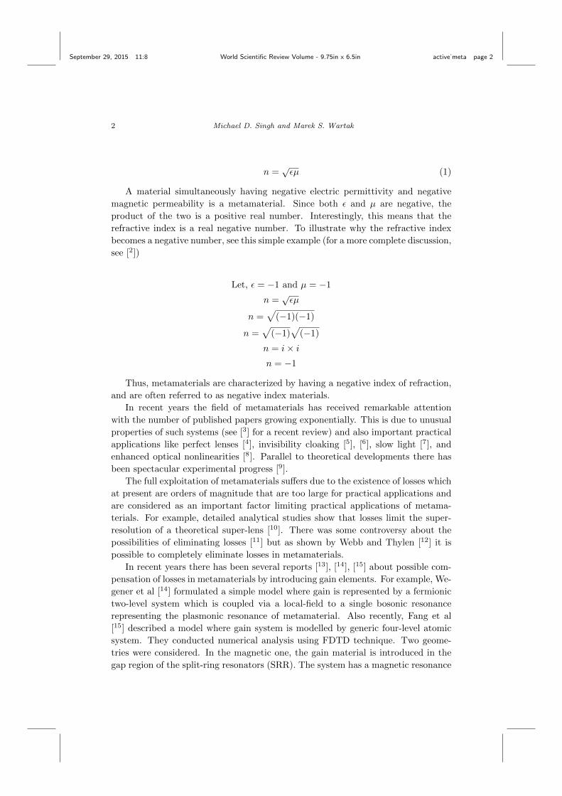
2.2. Fishnet Structures
A fishnet metamaterial structure is made of two very thin metallic layers, separated
by a thin dielectric slab, with periodically arrayed rectangular holes.22 This can be
seen in Fig. 2(a).
The goal is to achieve a simultaneously negative: electric permittivity and mag-
netic permeability, for a given frequency of incident light wave. A negative perme-
September 29, 2015 11:8 World Scientific Review Volume - 9.75in x 6.5in active˙meta page 4
4 Michael D. Singh and Marek S. Wartak
ability can be achieved if a strong magnetic resonance is formed at a frequency, ωm.23
Such a process can be described and analyzed using an inductance-capacitance (LC)
circuit where,
ωm =1√LC
(2)
For an incident optical signal, an (LC) circuit is formed in the fishnet structure
by the wire-dielectric-wire configuration that runs parallel to the incident magnetic
field whilst simultaneously inducing anti-parallel currents in the metallic layers on
either side of the dielectric slab.22 These two processes allow for the formation of
a magnetic field and ultimately a negative permeability through a strong magnetic
resonance between the incident and induced magnetic field.
A negative electric permittivity can be achieved through a system of parallel
wires separated by a dielectric slab. These parallel wires essentially exhibit plas-
monic behaviour similar to that of Drude metals.22,23 The permittivity then can
be represented by,
ε(ω) = 1−ω2p
ω2(3)
where ωp is the plasma frequency which can be tuned by changing the distance
between the wires (i.e., by changing the thickness of the dielectric slab). Thus from
equation 3, a slab thickness corresponding to an ωp value such that, ωp > ω, will
result in a negative electric permittivity (ε < 0). By viewing Fig. 2, it can be clearly
seen that parallel wires are separated by a dielectric slab in a fishnet structure, hence
providing a perfect environment for a negative electric permittivity.
Fig. 2. A fishnet structure with metallic layers on either side of a dielectric slab.
3. Applications
The growing popularity of metamaterial research can likely be attributed to the fas-
cinating potential applications. Among others, metamaterials have been proposed
September 29, 2015 11:8 World Scientific Review Volume - 9.75in x 6.5in active˙meta page 5
Active Metamaterials 5
to be capable of: storing light, breaking the diffraction limit or in other words;
achieving super-resolution, making objects invisible, and becoming nearly perfect
absorbers (optical black holes).
3.1. Photon Storage
Photon storage is of particular interest for storing qubits in memory for quantum
computing, i.e., quantum optical memory. Stopping light or even slowing it down
can provide a major technological boost in quantum electronics. Storing light has
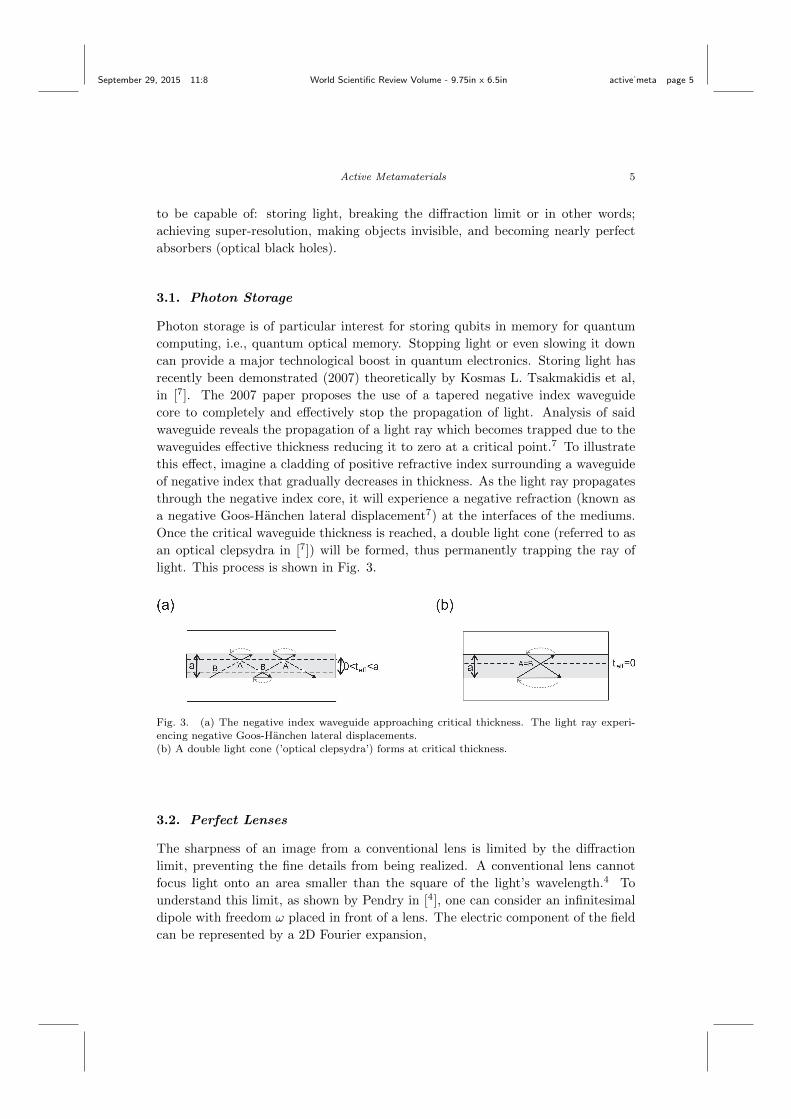
recently been demonstrated (2007) theoretically by Kosmas L. Tsakmakidis et al,
in [7]. The 2007 paper proposes the use of a tapered negative index waveguide
core to completely and effectively stop the propagation of light. Analysis of said
waveguide reveals the propagation of a light ray which becomes trapped due to the
waveguides effective thickness reducing it to zero at a critical point.7 To illustrate
this effect, imagine a cladding of positive refractive index surrounding a waveguide
of negative index that gradually decreases in thickness. As the light ray propagates
through the negative index core, it will experience a negative refraction (known as
a negative Goos-Hanchen lateral displacement7) at the interfaces of the mediums.
Once the critical waveguide thickness is reached, a double light cone (referred to as
an optical clepsydra in [7]) will be formed, thus permanently trapping the ray of
light. This process is shown in Fig. 3.
Fig. 3. (a) The negative index waveguide approaching critical thickness. The light ray experi-
(b) A double light cone (’optical clepsydra’) forms at critical thickness.
3.2. Perfect Lenses
The sharpness of an image from a conventional lens is limited by the diffraction
limit, preventing the fine details from being realized. A conventional lens cannot
focus light onto an area smaller than the square of the light’s wavelength.4 To
understand this limit, as shown by Pendry in [4], one can consider an infinitesimal
dipole with freedom ω placed in front of a lens. The electric component of the field
can be represented by a 2D Fourier expansion,
September 29, 2015 11:8 World Scientific Review Volume - 9.75in x 6.5in active˙meta page 6
6 Michael D. Singh and Marek S. Wartak
~E(~r, t) =∑
σ,kx,ky
~Eσ(kx, ky)× exp(ikzz + ikxx+ ikyy − iωt) (4)
Using Maxwell’s equations and choosing z to be the axis of the lens,
kz =
√ω2
c2− k2
x − k2y , where
ω2
c2> k2
x + k2y (5)
It is shown in [4] for large values of the transverse wave vector, that propagating
waves are limited to: k2x + k2
y <ω2
c2 such that,
kmax =ω2
c2(6)
then the maximum attainable resolution of an image is,
Rmax =2π
kmax=
2πc
ω=
2πc
2πf= λ , where ω = 2πf (7)
Thus it can clearly be seen that the maximum area one can focus light onto is
equal to λ2.
J. B. Pendry proposed in [4] that this limit in the optical range of a classical
lens can be surpassed using a negative index material (metamaterial).
As shown earlier, the refractive index of a medium will become negative if its
electric permittivity and magnetic permeability are simultaneously negative. How-
ever the impedance of the medium defined by,
Z =
√µµ0
εε0(8)
will remain positive.4 Moreover, if one selects values of ε = −1 and µ = −1,
the medium matches that of a vacuum space allowing for zero reflection at the
interface between vacuum and the negative index medium. At both boundaries of
the medium (entering and exiting the medium), the impedance match allows the
light to stay unchanged. The transmission coefficient of the negative index medium
turns out to be,
T = e−id√ω2c−2−k2x−k2y (9)
where d is the thickness of the metamaterial slab. This slab can prevent the
decay of evanescent waves by amplifying them, as shown in [4]. Sparing the intensive
details, after some analysis the transmission coefficient of the S-polarized waves
when the limit of ε and µ each approach −1 is taken, one obtains,
September 29, 2015 11:8 World Scientific Review Volume - 9.75in x 6.5in active˙meta page 7
Active Metamaterials 7
Ts = e−ikzd (10)
and similarly taking the same limit for P-polarized waves,
Tp = e−ikzd (11)
Thus amplification of evanescent waves is achievable using a negative index
medium. More importantly, the propagating waves as well as the evanescent waves
can contribute to the resolution of the image.4 This should be a point of emphasis
that theoretically speaking, a metamaterial lens can focus light onto an area smaller
than the square of the light’s wavelength.
Quite interestingly, it was proposed that the earlier mentioned limit can even be
broken using a thin slab of silver, which alone is not capable of achieving a negative
refractive index, only rather a negative electric permittivity given the correct design
parameters.
If one considers the dimensions of the silver slab to be smaller than the incident
light wavelength, known as the electrostatic limit where,
ω << c0
√k2x + k2
y (12)
the transmission coefficient of said slab, as shown in [4], is completely inde-
pendent of µ. Following the analysis in [4], the transmission coefficient in the
electrostatic limit turns out to be,
limk2x+k2y→∞
T =4εeikzd
(ε+ 1)2 − (ε− 1)2e2ikzd(13)
It can clearly be seen that the transmission is dependent on the electric permit-
tivity and independent of the magnetic permeability. Thus even a metal such as
silver, with a negative electric permittivity, can achieve image focusing beyond the
classical limit.
3.3. Invisibility
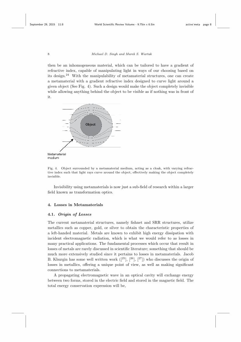
The prospect of making objects appear invisible is a fascinating idea that once
seemed to be of science fiction. Invisibility now appear to be a real possibility with
the advent of the field of metamaterials.
Typically, we are able to manipulate light with homogeneous materials such as
lenses to magnify and focus light to produce images.24 These homogeneous materials
generally have a uniform refractive index throughout. However, since metamaterials
consist of sub-wavelength elements to achieve their characteristic negative ε and µ,
one can arrange those elements in a way to produce a varying ε and µ, resulting
in a varying refractive index throughout the device. This metamaterial device will
September 29, 2015 11:8 World Scientific Review Volume - 9.75in x 6.5in active˙meta page 8
8 Michael D. Singh and Marek S. Wartak
then be an inhomogeneous material, which can be tailored to have a gradient of
refractive index, capable of manipulating light in ways of our choosing based on
its design.24 With the manipulability of metamaterial structures, one can create
a metamaterial with a gradient refractive index designed to curve light around a
given object (See Fig. 4). Such a design would make the object completely invisible
while allowing anything behind the object to be visible as if nothing was in front of
it.
Fig. 4. Object surrounded by a metamaterial medium, acting as a cloak, with varying refrac-tive index such that light rays curve around the object, effectively making the object completely
invisible.
Invisibility using metamaterials is now just a sub-field of research within a larger
field known as transformation optics.
4. Losses in Metamaterials
4.1. Origin of Losses
The current metamaterial structures, namely fishnet and SRR structures, utilize
metallics such as copper, gold, or silver to obtain the characteristic properties of
a left-handed material. Metals are known to exhibit high energy dissipation with
incident electromagnetic radiation, which is what we would refer to as losses in
many practical applications. The fundamental processes which occur that result in
losses of metals are rarely discussed in scientific literature; something that should be
much more extensively studied since it pertains to losses in metamaterials. Jacob
B. Khurgin has some well written work ([25], [26], [27]) who discusses the origin of
losses in metallics, offering a unique point of view, as well as making significant
connections to metamaterials.
A propagating electromagnetic wave in an optical cavity will exchange energy
between two forms, stored in the electric field and stored in the magnetic field. The
total energy conservation expression will be,
September 29, 2015 11:8 World Scientific Review Volume - 9.75in x 6.5in active˙meta page 9
Active Metamaterials 9
EE + EH = Etotal (14)
Substituting EE = 1/2εE2 and EH = 1/2µH2 to obtain,
1/2εE2 + 1/2µH2 = Etotal (15)
where E and H are the electric and magnetic field magnitudes, ε is the electric
permittivity, and µ is the magnetic permeability.
If free carriers are introduced (i.e., electrons), such as in a metal, it can be shown
that a third form of energy will enter the system in the form of carrier kinetic energy
(see [26], [27]). Equation 14 then becomes,
EE + EH + Ek = Etotal (16)
Subsequently, substituting Ek = 1/2ε0(ω2p/ω
2)E2, where ε0 is vacuum permit-
tivity, ω and ωp is the frequency and plasma frequency, respectively, to obtain,
1/2εE2 + 1/2µH2 + 1/2ε0(ω2p/ω
2)E2 = Etotal (17)
It can then be shown that the electric field energy, EE , is much greater than
the magnetic field energy, EH . In fact, for a confinement scale close to the plasma
wavelength, λp = 2πc/ωp, the magnetic field energy almost vanishes.25 Thus the
majority of the energy will be exchanged between the electric field and the kinetic
motion of electrons.25 It means that half of the time, nearly all of the energy of the
propagating electromagnetic field is stored in the form of carrier kinetic energy. This
kinetic energy eventually gets dissipated throughout the metal due to scattering by
defects and phonons at a rate of 2γ, where γ is the damping rate.26
4.2. Limitations of Loss Compensation
So far, reducing losses experienced by metamaterials has proven to be quite a chal-
lenging task. However, this has not deterred theorists and experimentalists alike
from attempting to achieve low-loss metamaterials which would unleash a plethora
of extraordinary technologies. As mentioned earlier, the main problem is the high
dissipative loss that occurs due to metallic layers used in the fabrication of a meta-
material device.
One technique to compensate metal loss in metamaterial, and currently probably
the most promising, is to introduce an active gain medium with sufficient pumping
parameters to achieve full compensation and even lasing.28 Loss compensation of a
metamaterial device through active gain media has been experimentally successful
through meticulous fabrication, which is discussed in Section 6. However, according
to Khurgin et al in [29], the only successful demonstration of internal miniature lasers
September 29, 2015 11:8 World Scientific Review Volume - 9.75in x 6.5in active˙meta page 10
10 Michael D. Singh and Marek S. Wartak
in plasmonic waveguides, so far, has been the ones which operate with optical pulses
rather than continuous signals and are always larger than half of the wavelength in
each structure in at least one direction.29
Currently, to the best of our knowledge, the only detailed theoretical analysis
of a gain integrated plasmonic waveguide was performed by Khurgin et al in [29].
They show that there appears to be general limitations for loss compensation and
lasing using active gain media. These apparent limitations should be studied much
more extensively and understood before attempting to create a loss compensation or
lasing environment. A review of the work by Khurgin et al in [29] will be presented.
Analysis on two different practical plasmonic waveguides with semiconductor
gain materials - one with a silver waveguide and one with a gold waveguide - re-
vealed two interesting findings. The first, pertains to tightly confining plasmonic
waveguides such that the confinement is much less than half the wavelength, the
modal loss was found to inevitably approach the loss of the metal itself, indepen-
dent of the geometry of the structure. The second shows that the current densities
necessary to achieve complete loss compensation approach unsustainable levels.
If one assumes that the total energy of light is stored in the kinetic energy of
carriers for half of a full oscillation, as shown Section 4.1. above, then the expression
for modal loss can be represented by,
γeff = γ(1− n−2eff ) (18)
where γ is the damping rate, and neff is the effective refractive index.
Calculations can be carried out and then γ and neff can be plotted as functions
of effective waveguide thickness. These plots can be seen in [29], showing that once
neff reaches a value of approximately 1.5, the modal loss is commensurate with the
metal loss i.e., 1014/s. The calculations assumed no specific geometry and therefore
the results are independent of geometry.
To compensate for this modal loss, the modal gain per second was represented
by,
g(ω) = B√~ω − Egap(fc(ω)− fv(ω))Γ (19)
where fc and fv are the Fermi-factors that depend on carrier density in the
conduction and valence bands, and B is the stimulated emission coefficient. The
confinement factor is expressed as,
Γ = 2qs
∫ da
0
e−2qsxdx (20)
where the thickness of the active layer was chosen to be da = 12qs, allowing for
a confinement factor value to be obtained.
The transparency carrier density, when g(ω) = γeff (ω), was then plotted as a
function of waveguide thickness yielding a reasonable range of: 1018 − 1019cm−3.
September 29, 2015 11:8 World Scientific Review Volume - 9.75in x 6.5in active˙meta page 11
Active Metamaterials 11
However, such transparency density range requires extremely high current densities,
i.e., 100 kA cm−2 for silver waveguides and 300 kA cm−2 for gold, at effective
waveguide thickness deff < 0.25. These current densities are at minimum two
orders of magnitude higher than threshold current densities in high powered double
heterostructure semiconductor lasers. The current density expression used in [29],
Jtr =4edaε
3/2s
cλ2BFp
∫ ∞Egap
√~ω − Egapfc(ω)(1− fv(ω))dω (21)
includes Purcells factor,
Fp = 1 + πΓqskxk3sω
(dkxdω
)(22)
which can get large due to the reduced group velocity and tight confinement
which resulted in decreased recombination times by orders of magnitude. See [29]
for specific numbers.
The current densities necessary to sustain full compensation and then lasing
seem to be impractically high. However it should be emphasized that though these
current densities seem to be unsustainable for continuous pumping, they are achiev-
able through optical pulsed pumping.
With all this said, it seems that more extensive research should be done in this
area to validate the work in [29]. There is much to learn about plasmonics and many
more configurations and new materials to explore.
5. Loss Reduction Schemes
Techniques for reducing loss in these left-handed materials are imperative in the field
of metamaterials. Many proposed techniques attempt to optimize the geometric
design of a given metamaterial in order to minimize energy dissipation.
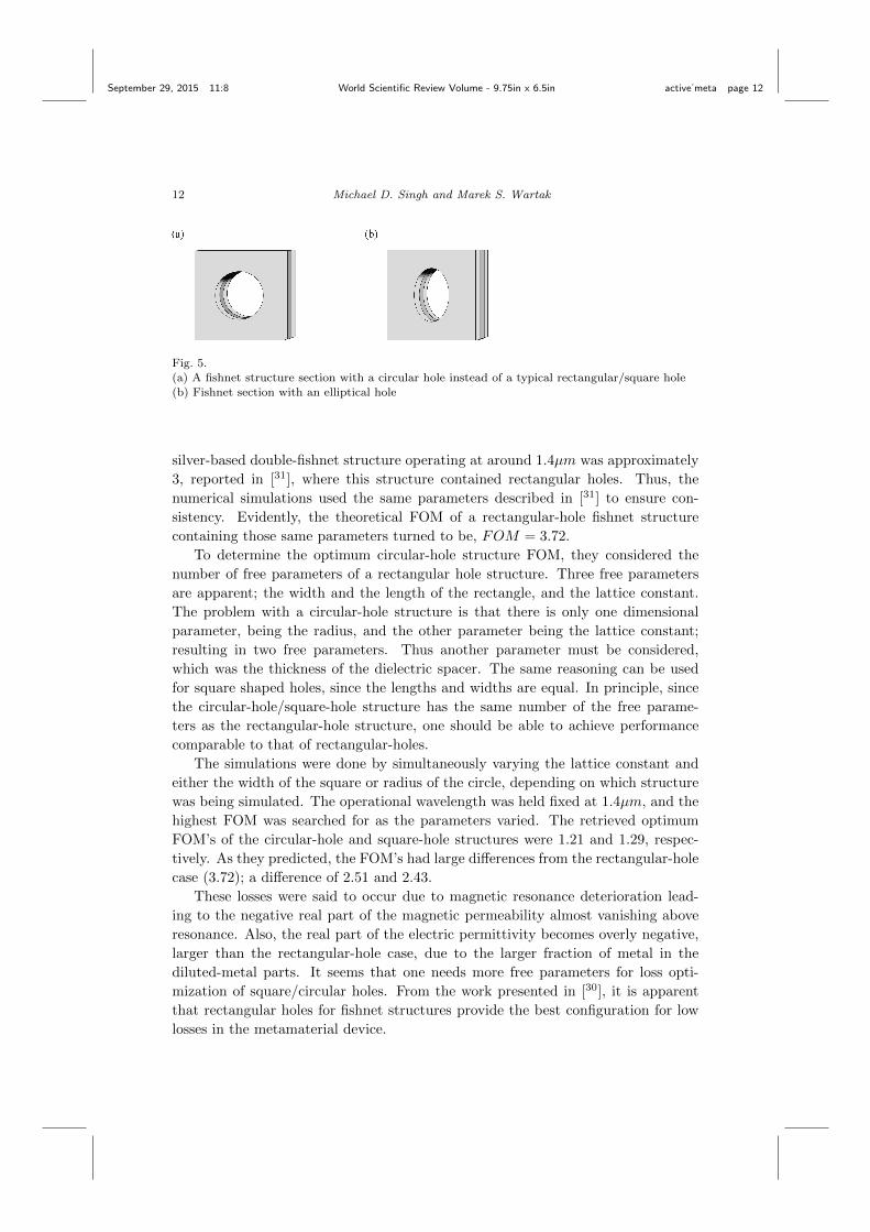
5.1. Effects of Different Hole Shapes
The double-fishnet structure currently seems to be the most effective fabrication of a
metamaterial device. As such, exploring various design characteristics of the fishnet
structures can provide useful information regarding loss reduction. In Fig. 2, the
holes of the fishnet structure are shown to be of square or rectangular nature. One
can also design a fishnet to have circular or elliptical holes (See Fig. 5). Another
design characteristic is the dielectric spacer thickness, as alluded to in the previous
section. The authors in [30] numerically analyze the effects on the figure of merit
(FOM) of a fishnet structure containing different shaped holes. The main finding
was that differing hole shapes can have a large impact on losses.
As a standard of comparison, Dolling et al in [30], used the highest experimen-
tally verified FOM. At the time of their writing, the highest achieved FOM of a
September 29, 2015 11:8 World Scientific Review Volume - 9.75in x 6.5in active˙meta page 12
12 Michael D. Singh and Marek S. Wartak
Fig. 5.(a) A fishnet structure section with a circular hole instead of a typical rectangular/square hole
(b) Fishnet section with an elliptical hole
silver-based double-fishnet structure operating at around 1.4µm was approximately
3, reported in [31], where this structure contained rectangular holes. Thus, the
numerical simulations used the same parameters described in [31] to ensure con-
sistency. Evidently, the theoretical FOM of a rectangular-hole fishnet structure
containing those same parameters turned to be, FOM = 3.72.
To determine the optimum circular-hole structure FOM, they considered the
number of free parameters of a rectangular hole structure. Three free parameters
are apparent; the width and the length of the rectangle, and the lattice constant.
The problem with a circular-hole structure is that there is only one dimensional
parameter, being the radius, and the other parameter being the lattice constant;
resulting in two free parameters. Thus another parameter must be considered,
which was the thickness of the dielectric spacer. The same reasoning can be used
for square shaped holes, since the lengths and widths are equal. In principle, since
the circular-hole/square-hole structure has the same number of the free parame-
ters as the rectangular-hole structure, one should be able to achieve performance
comparable to that of rectangular-holes.
The simulations were done by simultaneously varying the lattice constant and
either the width of the square or radius of the circle, depending on which structure
was being simulated. The operational wavelength was held fixed at 1.4µm, and the
highest FOM was searched for as the parameters varied. The retrieved optimum
FOM’s of the circular-hole and square-hole structures were 1.21 and 1.29, respec-
tively. As they predicted, the FOM’s had large differences from the rectangular-hole
case (3.72); a difference of 2.51 and 2.43.
These losses were said to occur due to magnetic resonance deterioration lead-
ing to the negative real part of the magnetic permeability almost vanishing above
resonance. Also, the real part of the electric permittivity becomes overly negative,
larger than the rectangular-hole case, due to the larger fraction of metal in the
diluted-metal parts. It seems that one needs more free parameters for loss opti-
mization of square/circular holes. From the work presented in [30], it is apparent
that rectangular holes for fishnet structures provide the best configuration for low
losses in the metamaterial device.
September 29, 2015 11:8 World Scientific Review Volume - 9.75in x 6.5in active˙meta page 13
Active Metamaterials 13
5.2. Loss Reduction via Geometric Tailoring
It has been proposed that ohmic losses can be reduced by geometrically tailoring a
metamaterial structure. This section will be an overview of the proposed technique
in [32].
5.2.1. Ohmic Loss in Left-Handed Materials
Ohmic loss of a metamaterial is the power dissipation resulting in heat production
due to resistance in the metallic layers of the structure.32 In the high frequency
range, the dominant loss component in a metamaterial is ohmic loss. Precisely mod-
ifying the geometric details of the structure can significantly change the amount of
ohmic loss experienced. In this way, field concentration and current distribution
will be affected with different curvatures and precise dimensional changes.32 A ge-
ometric tailoring technique is computationally demonstrated in [32] for split-ring
resonator (SRR) structures, however it should also be applicable to other metama-
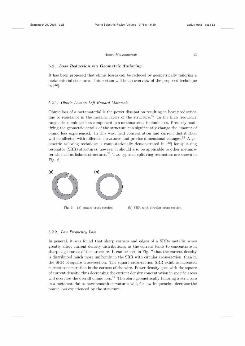
terials such as fishnet structures.32 Two types of split-ring resonators are shown in
Fig. 6.
Fig. 6. (a) square cross-section (b) SRR with circular cross-section
5.2.2. Low Frequency Loss
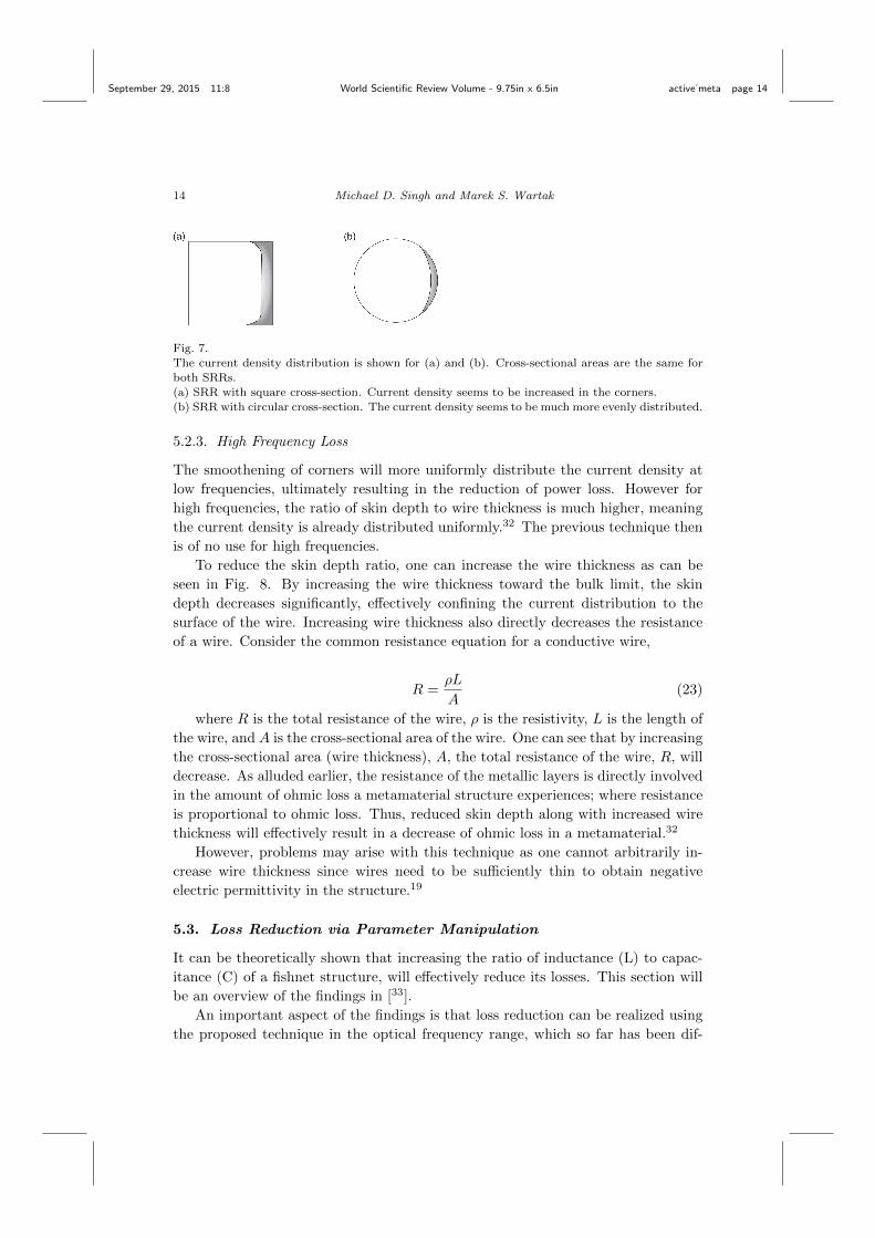
In general, it was found that sharp corners and edges of a SRRs metallic wires
greatly affect current density distributions, as the current tends to concentrate in
sharp edged areas of the structure. It can be seen in Fig. 7 that the current density
is distributed much more uniformly in the SRR with circular cross-section, than in
the SRR of square cross-section. The square cross-section SRR exhibits increased
current concentration in the corners of the wire. Power density goes with the square
of current density, thus decreasing the current density concentration in specific areas
will decrease the overall ohmic loss.32 Therefore geometrically tailoring a structure
in a metamaterial to have smooth curvatures will, for low frequencies, decrease the
power loss experienced by the structure.
September 29, 2015 11:8 World Scientific Review Volume - 9.75in x 6.5in active˙meta page 14
14 Michael D. Singh and Marek S. Wartak
Fig. 7.The current density distribution is shown for (a) and (b). Cross-sectional areas are the same for
both SRRs.
(a) SRR with square cross-section. Current density seems to be increased in the corners.(b) SRR with circular cross-section. The current density seems to be much more evenly distributed.
5.2.3. High Frequency Loss
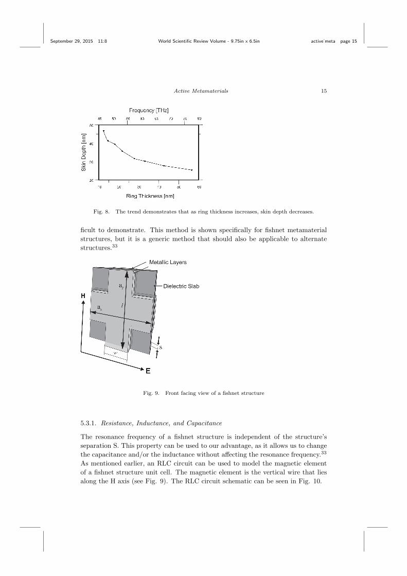
The smoothening of corners will more uniformly distribute the current density at
low frequencies, ultimately resulting in the reduction of power loss. However for
high frequencies, the ratio of skin depth to wire thickness is much higher, meaning
the current density is already distributed uniformly.32 The previous technique then
is of no use for high frequencies.
To reduce the skin depth ratio, one can increase the wire thickness as can be
seen in Fig. 8. By increasing the wire thickness toward the bulk limit, the skin
depth decreases significantly, effectively confining the current distribution to the
surface of the wire. Increasing wire thickness also directly decreases the resistance
of a wire. Consider the common resistance equation for a conductive wire,
R =ρL
A(23)
where R is the total resistance of the wire, ρ is the resistivity, L is the length of
the wire, and A is the cross-sectional area of the wire. One can see that by increasing
the cross-sectional area (wire thickness), A, the total resistance of the wire, R, will
decrease. As alluded earlier, the resistance of the metallic layers is directly involved
in the amount of ohmic loss a metamaterial structure experiences; where resistance
is proportional to ohmic loss. Thus, reduced skin depth along with increased wire
thickness will effectively result in a decrease of ohmic loss in a metamaterial.32
However, problems may arise with this technique as one cannot arbitrarily in-
crease wire thickness since wires need to be sufficiently thin to obtain negative
electric permittivity in the structure.19
5.3. Loss Reduction via Parameter Manipulation
It can be theoretically shown that increasing the ratio of inductance (L) to capac-
itance (C) of a fishnet structure, will effectively reduce its losses. This section will
be an overview of the findings in [33].
An important aspect of the findings is that loss reduction can be realized using
the proposed technique in the optical frequency range, which so far has been dif-
September 29, 2015 11:8 World Scientific Review Volume - 9.75in x 6.5in active˙meta page 15
Active Metamaterials 15
Fig. 8. The trend demonstrates that as ring thickness increases, skin depth decreases.
ficult to demonstrate. This method is shown specifically for fishnet metamaterial
structures, but it is a generic method that should also be applicable to alternate
structures.33
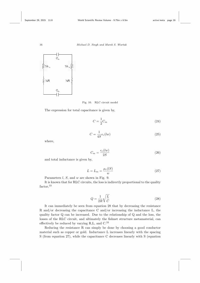
Fig. 9. Front facing view of a fishnet structure
5.3.1. Resistance, Inductance, and Capacitance
The resonance frequency of a fishnet structure is independent of the structure’s
separation S. This property can be used to our advantage, as it allows us to change
the capacitance and/or the inductance without affecting the resonance frequency.33
As mentioned earlier, an RLC circuit can be used to model the magnetic element
of a fishnet structure unit cell. The magnetic element is the vertical wire that lies
along the H axis (see Fig. 9). The RLC circuit schematic can be seen in Fig. 10.
September 29, 2015 11:8 World Scientific Review Volume - 9.75in x 6.5in active˙meta page 16
16 Michael D. Singh and Marek S. Wartak
Fig. 10. RLC circuit model
The expression for total capacitance is given by,
C =1
2Cm (24)
C =1
4Sεr(lw) (25)
where,
Cm =εr(lw)
2S(26)
and total inductance is given by,
L = Lm =µr(lS)
w(27)
Parameters l, S, and w are shown in Fig. 9.
It is known that for RLC circuits, the loss is indirectly proportional to the quality
factor,33
Q =1
2R
√L
C(28)
It can immediately be seen from equation 28 that by decreasing the resistance
R and/or decreasing the capacitance C and/or increasing the inductance L, the
quality factor Q can be increased. Due to the relationship of Q and the loss, the
losses of the RLC circuit, and ultimately the fishnet structure metamaterial, can
effectively be reduced by varying R,L, and C.33
Reducing the resistance R can simply be done by choosing a good conductor
material such as copper or gold. Inductance L increases linearly with the spacing
S (from equation 27), while the capacitance C decreases linearly with S (equation
September 29, 2015 11:8 World Scientific Review Volume - 9.75in x 6.5in active˙meta page 17
Active Metamaterials 17
26). These proportionalities work in our favour. One can increase the thickness of
the dielectric slab which increases the spacing between the metallic layers, which
will increase the inductance while simultaneously decreasing the capacitance.
Increasing the separation S cannot be done arbitrarily, as it is restricted by the
unit cell az which can be defined from Fig. 9 as the perpendicular vector to ax and
ay. The separation can go no larger than az, and az must be much smaller than the
wavelength of electromagnetic radiation.33 It must also be kept small enough to
not affect the negative electric permittivity of the long wires.33 Another potential
problem occurs according to the computational findings in [33] that the magnetic
resonance disappears after the spacing is increased to a certain value larger than
the width of the wires. This apparently occurs because the short wires decouple
from each other at that critical value.33
5.4. Optical Parametric Amplification
Optical parametric amplification was theoretically proposed in [34] as a means of
compensating loss in negative index materials. The scheme utilizes a positive-index
auxiliary electromagnetic field signal as a control field which enables a loss-balancing
optical parametric amplification for a negative-index signal wave.34 This section will
present a review of the proposed loss compensation scheme.
The setup considers a negative-index wave signal of frequency ω1 which has a
wave vector ~k1 in the positive direction, let us say along the z-axis. This negative-
index signal’s Poynting vector ~S1 is anti-parallel to ~k1; directed against the z-
axis. The auxiliary control signal travels in a positive-index domain, and hence is a
positive-index signal along the z-axis with frequency ω3 and wave vector ~k3. This
positive-index wave has a Poynting vector ~S3 which is directed parallel to ~k3. The
two coupled waves with parallel wave vectors ~k1 and ~k3 will give rise to an idle wave
of frequency, ω2 = ω3−ω1, that travels in the positive-index domain. The idle wave
then has a wave vector ~k2 and a Poynting vector ~S2 that travel along the z-axis.
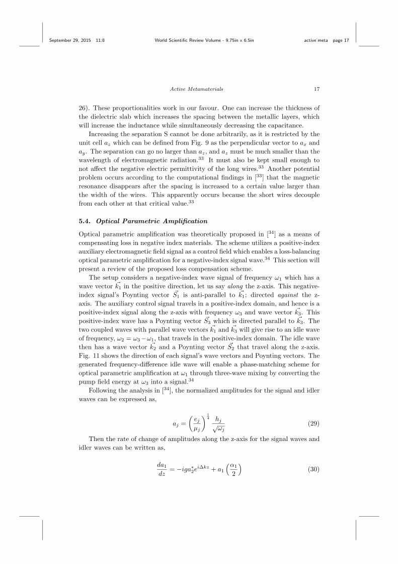
Fig. 11 shows the direction of each signal’s wave vectors and Poynting vectors. The
generated frequency-difference idle wave will enable a phase-matching scheme for
optical parametric amplification at ω1 through three-wave mixing by converting the
pump field energy at ω3 into a signal.34
Following the analysis in [34], the normalized amplitudes for the signal and idler
waves can be expressed as,
aj =
(ejµj
) 14 hj√
ωj(29)
Then the rate of change of amplitudes along the z-axis for the signal waves and
idler waves can be written as,
da1
dz= −iga∗2ei∆kz + a1
(α1
2
)(30)
September 29, 2015 11:8 World Scientific Review Volume - 9.75in x 6.5in active˙meta page 18
18 Michael D. Singh and Marek S. Wartak
Fig. 11. The direction of each signal’s wave vectors and Poynting vectors. L is the slab thickness.
da2
dz= −iga∗1ei∆kz − a2
(α2
2
)(31)
where,
g =√ω1ω2
(ε1ε2µ1µ2
)− 14(
8π
c
)χ(2)h3 (32)
and ∆k = k3 − k2 − k1. The pump amplitude h3 is assumed to be a constant,
αj are the absorption coefficients. The values a21 and a2
2 are proportional to the
number of photons at each corresponding frequency.
Using boundary conditions: a1(L) = a1L and a2(0) = a20 where L is the slab
thickness, one can solve Equations 30 and 31 to obtain solutions,
a1(z) = A1eβ+1 z +A2e
β+2 z (33)
a∗2(z) = κ1A1eβ−1 z + κ2A2e
β−2 z (34)
where
β±1,2 = β1,2 ± (i∆k/2) and β1,2 =1
4(α1 − α2)± iR
A1,2 = ± 1
D
[a1Lκ2,1 − a∗20e
β+2,1L]
D = κ2eβ+1 L − κ1e
β+2 L
κ1,2 =1
g(±R+ is) and R =
√g2 − s2
s =1
4(α1 + α2)− i∆k/2
September 29, 2015 11:8 World Scientific Review Volume - 9.75in x 6.5in active˙meta page 19
Active Metamaterials 19
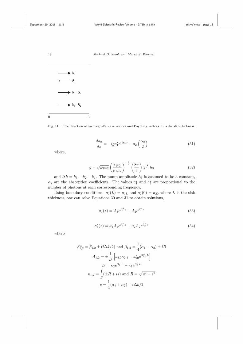
Fig. 12. The output amplification factor, η1a, plotted against gL
Then the amplification factor is,
η1a(z) =
∣∣∣∣a1(z)
a1L
∣∣∣∣2 (35)
and for the case a1L = 0,
η1a(z) =
∣∣∣∣a1(z)
a20
∗∣∣∣∣2 (36)
Upon simulation, resulting graphs show that amplification of several orders of
magnitude occurs for phase-matched waves. Fig. 12 shows a plot of the output
amplification factor, η1a, versus gL, where g is from equation 5.4. Such amplification
can provide complete loss compensation of a metamaterial medium.
6. Active Gain
Gain in metamaterials can be incorporated utilizing fluorescent dyes,35 quantum
dots,36,37 quantum wells,38.39 Several metallic structures were investigated, includ-
ing SRR, inverted SRR, fishnets. Gain material is typically modelled as a four-level
system,40.41
A simple model of plasmonic material with gain known as toy model14 will now
be summarized. The model can provide some general insight about the influence of
gain.
6.1. Toy model
Several years ago a simple model of a metamaterial incorporating optical gain was
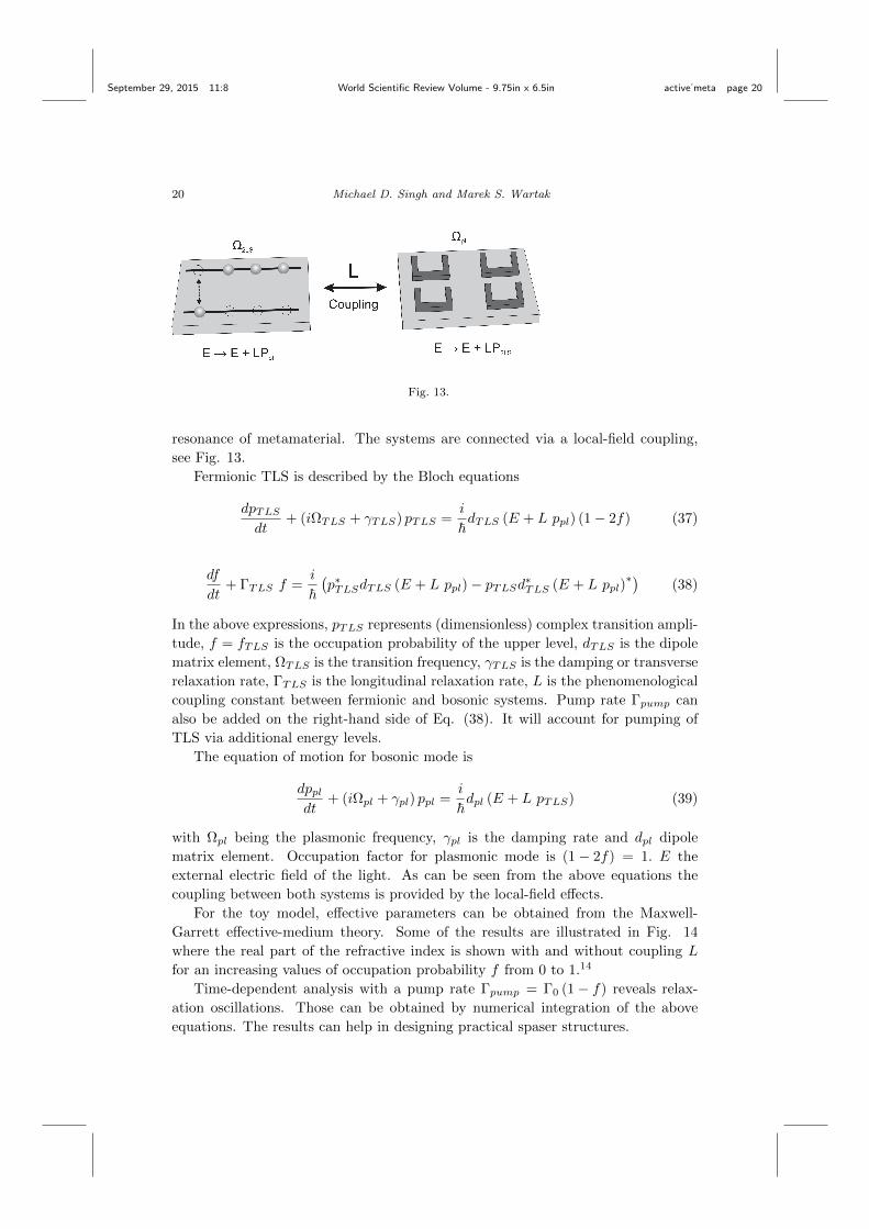
proposed by Wegener et al.14 It consists of a fermionic two-level system (TLS) which
represents gain medium and a single bosonic resonance which represents plasmonic
September 29, 2015 11:8 World Scientific Review Volume - 9.75in x 6.5in active˙meta page 20
20 Michael D. Singh and Marek S. Wartak
Fig. 13.
resonance of metamaterial. The systems are connected via a local-field coupling,
see Fig. 13.
Fermionic TLS is described by the Bloch equations
dpTLSdt
+ (iΩTLS + γTLS) pTLS =i
~dTLS (E + L ppl) (1− 2f) (37)
df
dt+ ΓTLS f =
i
~(p∗TLSdTLS (E + L ppl)− pTLSd∗TLS (E + L ppl)
∗)(38)
In the above expressions, pTLS represents (dimensionless) complex transition ampli-
tude, f = fTLS is the occupation probability of the upper level, dTLS is the dipole
matrix element, ΩTLS is the transition frequency, γTLS is the damping or transverse
relaxation rate, ΓTLS is the longitudinal relaxation rate, L is the phenomenological
coupling constant between fermionic and bosonic systems. Pump rate Γpump can
also be added on the right-hand side of Eq. (38). It will account for pumping of
TLS via additional energy levels.
The equation of motion for bosonic mode is
dppldt
+ (iΩpl + γpl) ppl =i
~dpl (E + L pTLS) (39)
with Ωpl being the plasmonic frequency, γpl is the damping rate and dpl dipole
matrix element. Occupation factor for plasmonic mode is (1− 2f) = 1. E the
external electric field of the light. As can be seen from the above equations the
coupling between both systems is provided by the local-field effects.
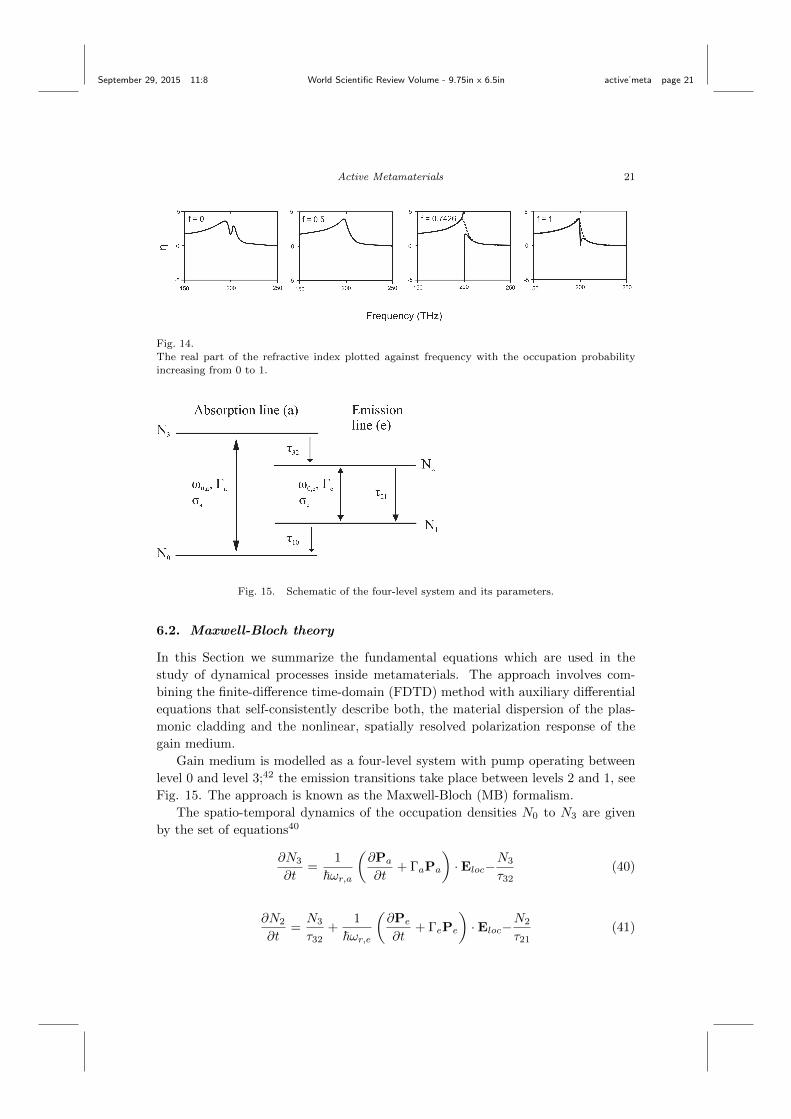
For the toy model, effective parameters can be obtained from the Maxwell-
Garrett effective-medium theory. Some of the results are illustrated in Fig. 14
where the real part of the refractive index is shown with and without coupling L
for an increasing values of occupation probability f from 0 to 1.14
Time-dependent analysis with a pump rate Γpump = Γ0 (1− f) reveals relax-
ation oscillations. Those can be obtained by numerical integration of the above
equations. The results can help in designing practical spaser structures.
September 29, 2015 11:8 World Scientific Review Volume - 9.75in x 6.5in active˙meta page 21
Active Metamaterials 21
Fig. 14.
The real part of the refractive index plotted against frequency with the occupation probabilityincreasing from 0 to 1.
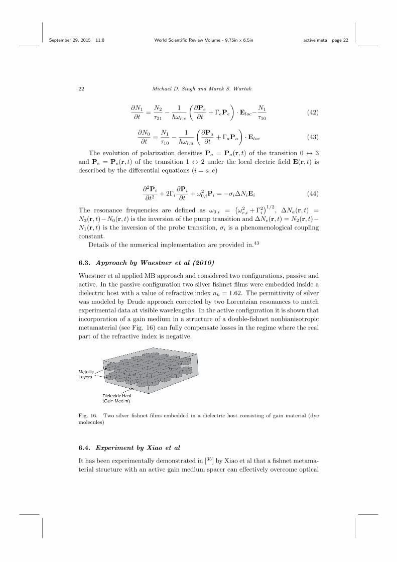
Fig. 15. Schematic of the four-level system and its parameters.
6.2. Maxwell-Bloch theory
In this Section we summarize the fundamental equations which are used in the
study of dynamical processes inside metamaterials. The approach involves com-
bining the finite-difference time-domain (FDTD) method with auxiliary differential
equations that self-consistently describe both, the material dispersion of the plas-
monic cladding and the nonlinear, spatially resolved polarization response of the
gain medium.
Gain medium is modelled as a four-level system with pump operating between
level 0 and level 3;42 the emission transitions take place between levels 2 and 1, see
Fig. 15. The approach is known as the Maxwell-Bloch (MB) formalism.
The spatio-temporal dynamics of the occupation densities N0 to N3 are given
by the set of equations40
∂N3
∂t=
1
~ωr,a
(∂Pa∂t
+ ΓaPa
)·Eloc−
N3
τ32(40)
∂N2
∂t=N3
τ32+
1
~ωr,e
(∂Pe∂t
+ ΓePe
)·Eloc−
N2
τ21(41)
September 29, 2015 11:8 World Scientific Review Volume - 9.75in x 6.5in active˙meta page 22
22 Michael D. Singh and Marek S. Wartak
∂N1
∂t=N2
τ21− 1
~ωr,e
(∂Pe∂t
+ ΓePe
)·Eloc−
N1
τ10(42)
∂N0
∂t=N1
τ10− 1
~ωr,a
(∂Pa∂t
+ ΓaPa
)·Eloc (43)
The evolution of polarization densities Pa = Pa(r, t) of the transition 0 ↔ 3
and Pe = Pe(r, t) of the transition 1 ↔ 2 under the local electric field E(r, t) is
described by the differential equations (i = a, e)
∂2Pi∂t2
+ 2Γi∂Pi∂t
+ ω20,iPi = −σi∆NiEi (44)
The resonance frequencies are defined as ω0,i =(ω2r,i + Γ2
i
)1/2, ∆Na(r, t) =
N3(r, t)−N0(r, t) is the inversion of the pump transition and ∆Ne(r, t) = N2(r, t)−N1(r, t) is the inversion of the probe transition, σi is a phenomenological coupling
constant.
Details of the numerical implementation are provided in.43
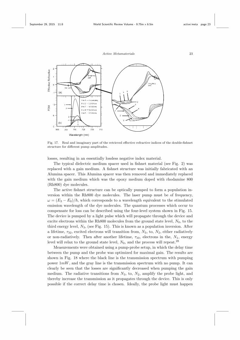
6.3. Approach by Wuestner et al (2010)
Wuestner et al applied MB approach and considered two configurations, passive and
active. In the passive configuration two silver fishnet films were embedded inside a
dielectric host with a value of refractive index nh = 1.62. The permittivity of silver
was modeled by Drude approach corrected by two Lorentzian resonances to match
experimental data at visible wavelengths. In the active configuration it is shown that
incorporation of a gain medium in a structure of a double-fishnet nonbianisotropic
metamaterial (see Fig. 16) can fully compensate losses in the regime where the real
part of the refractive index is negative.
Fig. 16. Two silver fishnet films embedded in a dielectric host consisting of gain material (dyemolecules)
6.4. Experiment by Xiao et al
It has been experimentally demonstrated in [35] by Xiao et al that a fishnet metama-
terial structure with an active gain medium spacer can effectively overcome optical
September 29, 2015 11:8 World Scientific Review Volume - 9.75in x 6.5in active˙meta page 23
Active Metamaterials 23
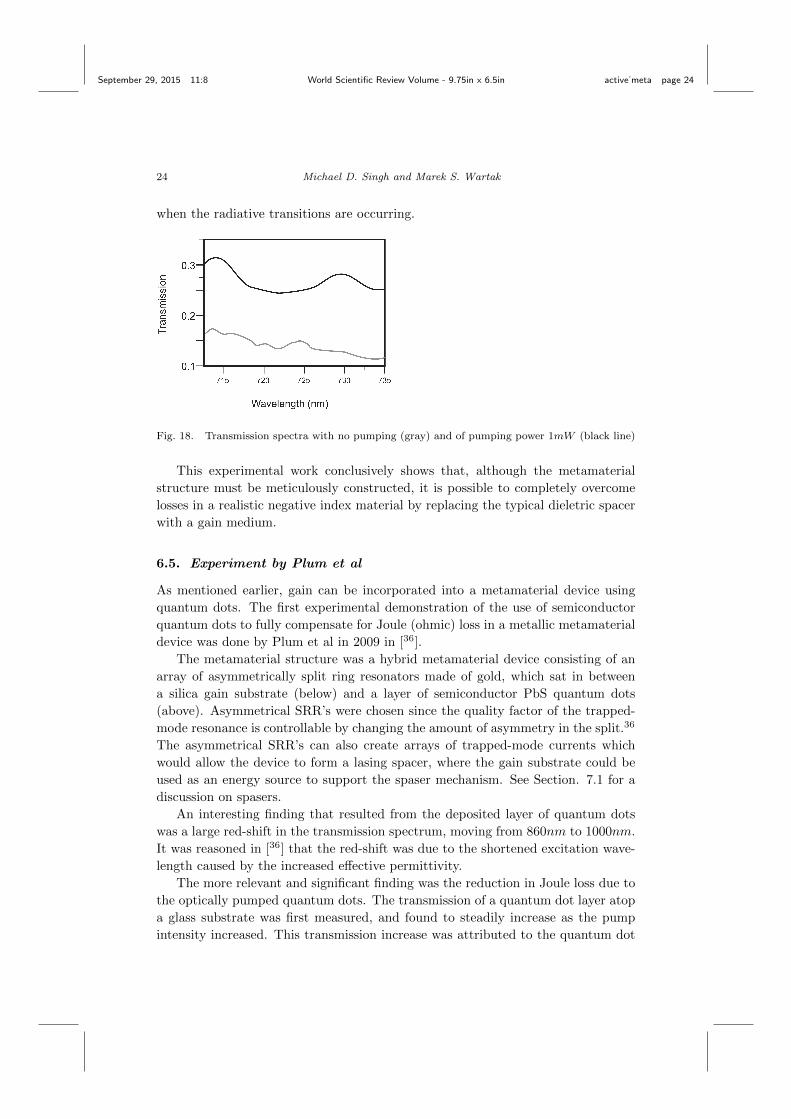
Fig. 17. Real and imaginary part of the retrieved effective refractive indices of the double-fishnetstructure for different pump amplitudes.
losses, resulting in an essentially lossless negative index material.
The typical dielectric medium spacer used in fishnet material (see Fig. 2) was
replaced with a gain medium. A fishnet structure was initially fabricated with an
Alumina spacer. This Alumina spacer was then removed and immediately replaced
with the gain medium which was the epoxy medium doped with rhodamine 800
(Rh800) dye molecules.
The active fishnet structure can be optically pumped to form a population in-
version within the Rh800 dye molecules. The laser pump must be of frequency,
ω = (E3 − E0)/~, which corresponds to a wavelength equivalent to the stimulated
emission wavelength of the dye molecules. The quantum processes which occur to
compensate for loss can be described using the four-level system shown in Fig. 15.
The device is pumped by a light pulse which will propagate through the device and
excite electrons within the Rh800 molecules from the ground state level, N0, to the
third energy level, N3, (see Fig. 15). This is known as a population inversion. After
a lifetime, τ32, excited electrons will transition from, N3, to, N2, either radiatively
or non-radiatively. Then after another lifetime, τ10, electrons in the, N1, energy
level will relax to the ground state level, N0, and the process will repeat.28
Measurements were obtained using a pump-probe setup, in which the delay time
between the pump and the probe was optimized for maximal gain. The results are
shown in Fig. 18 where the black line is the transmission spectrum with pumping
power 1mW , and the gray line is the transmission spectrum with no pump. It can
clearly be seen that the losses are significantly decreased when pumping the gain
medium. The radiative transitions from N3, to, N2, amplify the probe light, and
thereby increase the transmission as it propagates through the device. This is only
possible if the correct delay time is chosen. Ideally, the probe light must happen
September 29, 2015 11:8 World Scientific Review Volume - 9.75in x 6.5in active˙meta page 24
24 Michael D. Singh and Marek S. Wartak
when the radiative transitions are occurring.
Fig. 18. Transmission spectra with no pumping (gray) and of pumping power 1mW (black line)
This experimental work conclusively shows that, although the metamaterial
structure must be meticulously constructed, it is possible to completely overcome
losses in a realistic negative index material by replacing the typical dieletric spacer
with a gain medium.
6.5. Experiment by Plum et al
As mentioned earlier, gain can be incorporated into a metamaterial device using
quantum dots. The first experimental demonstration of the use of semiconductor
quantum dots to fully compensate for Joule (ohmic) loss in a metallic metamaterial
device was done by Plum et al in 2009 in [36].
The metamaterial structure was a hybrid metamaterial device consisting of an
array of asymmetrically split ring resonators made of gold, which sat in between
a silica gain substrate (below) and a layer of semiconductor PbS quantum dots
(above). Asymmetrical SRR’s were chosen since the quality factor of the trapped-
mode resonance is controllable by changing the amount of asymmetry in the split.36
The asymmetrical SRR’s can also create arrays of trapped-mode currents which
would allow the device to form a lasing spacer, where the gain substrate could be
used as an energy source to support the spaser mechanism. See Section. 7.1 for a
discussion on spasers.
An interesting finding that resulted from the deposited layer of quantum dots
was a large red-shift in the transmission spectrum, moving from 860nm to 1000nm.
It was reasoned in [36] that the red-shift was due to the shortened excitation wave-
length caused by the increased effective permittivity.
The more relevant and significant finding was the reduction in Joule loss due to
the optically pumped quantum dots. The transmission of a quantum dot layer atop
a glass substrate was first measured, and found to steadily increase as the pump
intensity increased. This transmission increase was attributed to the quantum dot
September 29, 2015 11:8 World Scientific Review Volume - 9.75in x 6.5in active˙meta page 25
Active Metamaterials 25
luminescence. When the quantum dots within the hybrid metamaterial device were
optically pumped, the transmission spectrum at the trapped mode resonance fre-
quency was significantly altered, in the background of quantum dot luminescence.
The transmission spectrum modification was separated from the quantum dot lu-
minescence which depended upon pump intensity, by introducing pump-induced
change of the differential transmission signal for two perpendicular polarizations,
which was then plotted. It can clearly be seen (see [36]) that the luminescence
signal has no dependence on the polarization of the probe light used to measure
the transmission. Thus, it can be concluded that any change in the transmission
spectrum is solely caused by gain in the metamaterial device. It was argued that
the gain must occur due to the strong interaction between the optically pumped
quantum dot layer and surface plasmon modes.
Thus, Plum et al have shown that by creating a hybrid metamaterial device
with an optically pumped quantum dot layer, one can effectively reduce Joule loss
within the device.
6.6. Powered Active Metamaterial Cells
Experiments have successfully shown loss compensation through powered active
cells, however only in unrealistic configurations.16 Yuan et al in [16] were able to
experimentally demonstrate a realistic tunable powered active-magnetic metamate-
rial, capable of completely compensating for loss at certain frequencies.
The reasoning in [16] for their design considered the magnetic moment of a unit
cell and the resulting effective magnetic permeability. The relationship between
the magnetic field, ~B, and the magnetic field strength, ~H, where magneto-electro
coupling is nonexistent, can be expressed as,
~B = µ0( ~H + ~M) (45)
where ~M is the magnetization vector. Using equation 45, and recognizing the
relation,
~B = µ0µr ~H (46)
one can determine the relative permeability tensor. Assuming ~B, ~H, and ~M are
colinear, the relavant component of the permeability tensor can be expressed by,
µr = 1 +~M
~H(47)
where magnetization ~M is the resulting magnetic moment due to the magnetic
strength field, ~H, and thus can be given by,
~M = |M |eiφ (48)
September 29, 2015 11:8 World Scientific Review Volume - 9.75in x 6.5in active˙meta page 26
26 Michael D. Singh and Marek S. Wartak
where φ is the phase of ~M with respect to ~H.
Using [44] as a reference, the authors in [16] recognized that control of the phase
φ from equation 48 enables control of the real and imaginary parts of the magnetic
permeability. The design of the metamaterial device used this fact to enable for
high tunability.
The experiment utilized an active-magnetic metamaterial consisting of arrays of
unit cells, where each unit cell was powered by a DC supply. The unit cell design
was inspired by the work in [44]. Each unit cell comprised of a sensing loop for
the incident magnetic field, a radiofrequency (RF) amplifier to amplify the sensed
signal, and a driven loop in order to tune the magnetization vector ~M . Adjacent
to the sensing and driven loops was an SRR, which reduced the amount of active
gain required for the device.16 The RF amplifier inputs a signal into a voltage-
controlled phase shifter which controls the phase at the driven loop. The phase
shifter turns out to be of high importance as it distinguishes the unit cell from
any other previously designed powered active metamaterial. This phase shifter is
ultimately responsible for controlling the real and imaginary parts of the effective
magnetic permeability. Since the phase shifter is voltage-controlled, the unit cell
then has a highly tunable magnetic permeability property. This unique design and
capability can be of great significance when considering loss in the magnetic regime
of a metamaterial device.
Upon testing a single unit cell by applying DC bias voltages ranging from 0V to
12V, it was found that at each applied voltage there was a strong magnetic response
just above the self resonant frequencies of the SRRs. Zero magnetic loss frequencies
were found at corresponding points of real (µ′
r) and imaginary (µ′′
r ) permeability,
at specific bias voltages. More interestingly, at certain µ′
r and µ′′
r , it was found that
zero magnetic loss is possible for an array of unit cells. However, one cannot choose
an arbitrary frequency as it was found that the electric response can become large,
resulting in a device that exhibits zero magnetic loss but nonzero overall loss. For
certain frequencies, the electric antiresonance is negligible allowing the material to
be completely lossless. See [16] for specific numbers and figures.
The authors in [16] experimentally demonstrated loss compensation of a realistic
metamaterial device, albeit only for certain frequencies. This work however provides
a great step forward for low-loss metamaterials.
7. Surface Plasmons
Surface plasmons (SPs) can be described as collective and coherent oscillations
of electron-fields confined to the surface of a medium. Plasmons are collective
oscillations of a free electron gas within a medium, away from the surface. Metallics
in particular have surface plasmons that are tightly bound to the surface, which
makes them effective scatterers of incident electromagnetic waves.45 As mentioned
in Section 4., much of the energy of electromagnetic waves gets dissipated by the
September 29, 2015 11:8 World Scientific Review Volume - 9.75in x 6.5in active˙meta page 27
Active Metamaterials 27
kinetic energy of electrons. This kinetic energy is usually in the form of coherent
oscillations, i.e., (surface) plasmons.
Surface plasmons can also propagate along the surface of metals, reaching dis-
tances of up to several hundreds of microns.45 Since propagating SPs are moving
charges, an electromagnetic wave is generated on the interface of the metal and
dielectric. These propagating electromagnetic field waves which couple with the
moving SPS are known as surface plasmon polaritons (SPPs).45
7.1. Spaser
The spaser (acronym for ”surface plasmon amplification by stimulated emission of
radiation”) device was first proposed by Bergman and Stockman in 2003. A spacer
is analogous to a laser, the main difference being that, as the name suggests, a
spaser emits surface plasmons instead of photons. The resonant cavity of a spaser
is a nanoparticle, such as a semiconductor quantum dot. An externally excited gain
medium can then be used as the energy source for spasing to occur.46
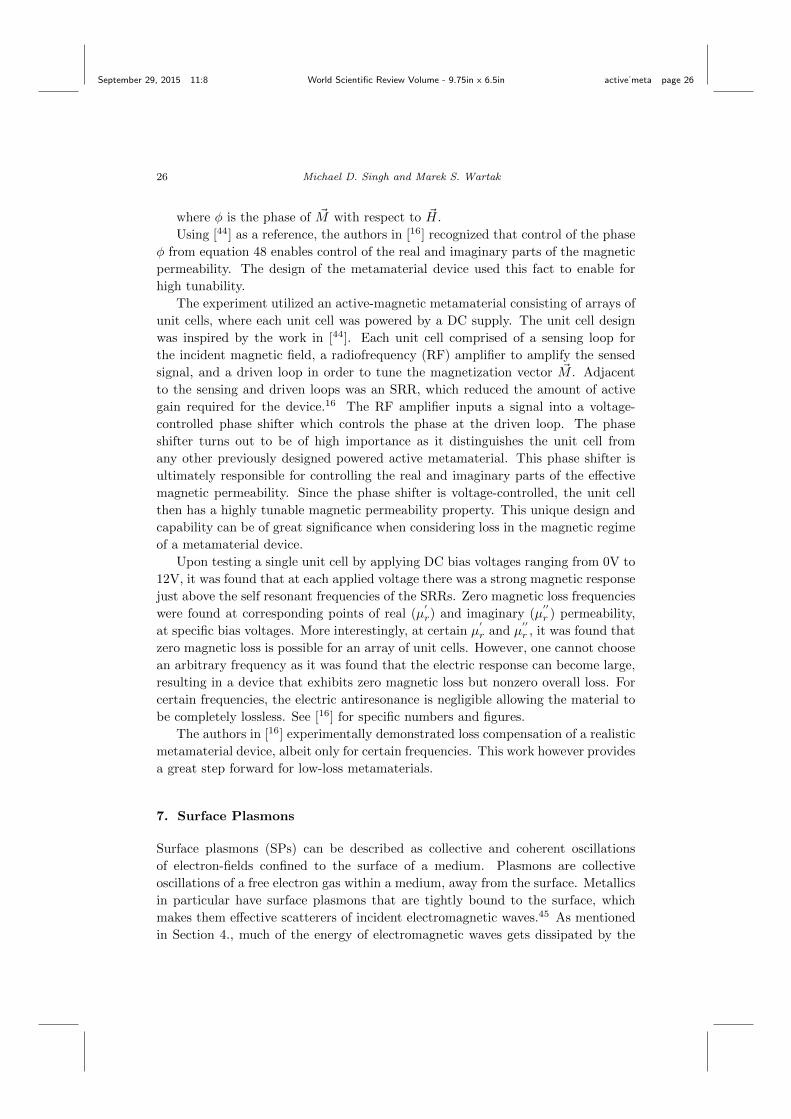
Stockman proposed a particular design of a spacer in [46] to consist of a dielec-
tric core surrounded by a silver nanoshell, which was then surrounded by a few
monolayers of nanocrystal quantum dots (NQD) (see Fig. 19). The dielectric core
surrounded by the silver nanoshell would then act as the resonant nanoparticle and
the NQDs would act as the gain medium.
Fig. 19. Proposed spaser setup with an interior dielectric core surrounded by a silver shell whichis surrounded by nanocrystal quantum dots
The idea is to use an external optical radiation source to excite an electron-hole
pair from an NQD, which will eventually relax into an excitonic level state due to
carrier multiplication.46 Typically the recombination of an exciton would result in
the generation of a photon, however since the NQDs are in contact with a resonant
nanoparticle, the energy is transferred virtually radiationless to the resonant SPs
of the nanoparticle. The excited SPs will then continue to stimulate electron-hole
transitions from the gain medium, which will in turn excite more SPs.46 This is
precisely the process of a spaser.
September 29, 2015 11:8 World Scientific Review Volume - 9.75in x 6.5in active˙meta page 28
28 Michael D. Singh and Marek S. Wartak
7.2. Metamaterial Lasing Spaser
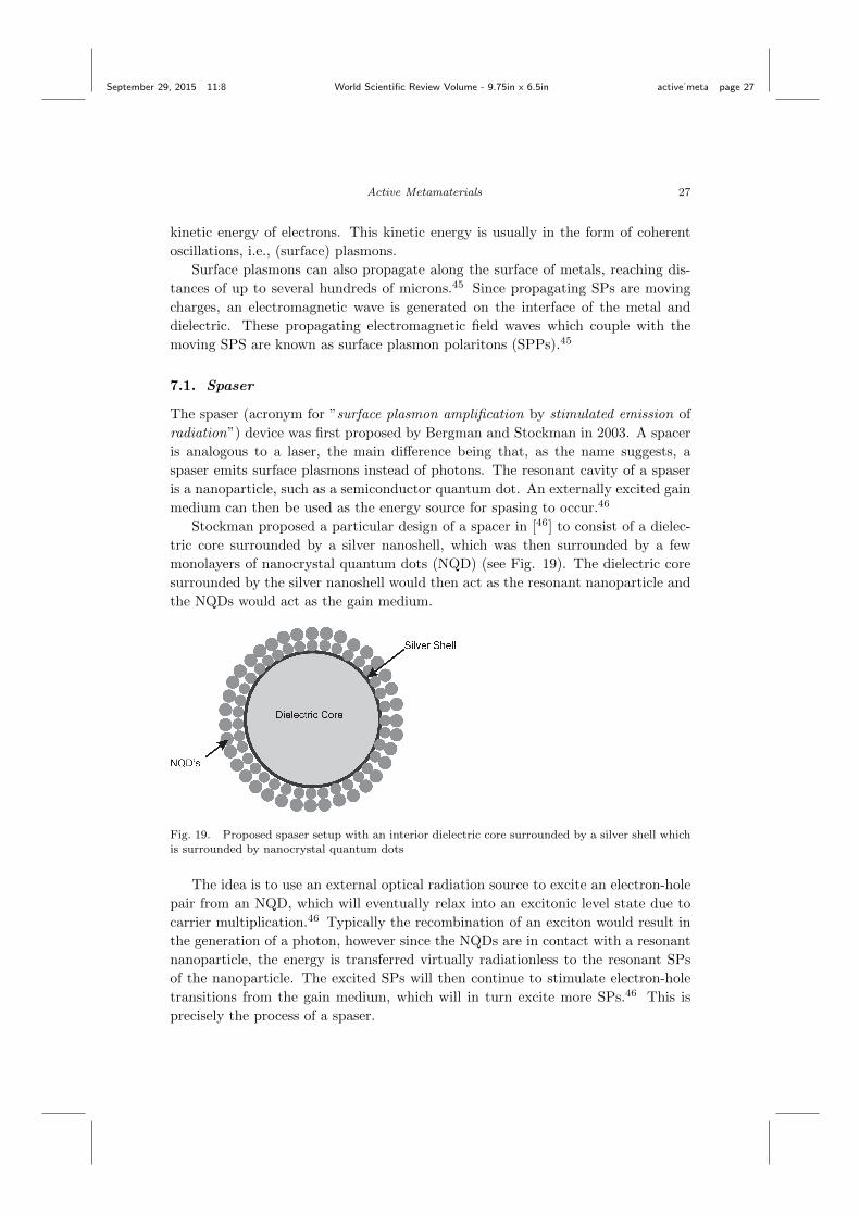
Zheludev et al combined the concepts of spasers along with metamaterials in [47] to
propose a metamaterial lasing device which uses plasmonic oscillations to generate
a coherent source of electromagnetic radiation. The proposed device consists of a
slab of gain medium containing an array of metallic asymmetric split-ring resonators
(See Fig. 20).
Fig. 20. Slab of gain medium containing an array of metallic asymmetric SRR’s
This array must be a special type of metamaterial array of plasmonic resonators
that support a high quality factor for current oscillations in which total emission
losses for the in-phase oscillations are at a minimum. These metamaterial arrays
were referred to as coherent metamaterials. It was recently shown in [48] that
SRR’s with weak antisymmetry may be excited by a high-quality mode of intense
anti-symmetric current oscillations.47
The active medium of the lasing spaser is the combination of the electromag-
netic resonators where the supporting gain substrate is the energy source. Since
the trapped-mode oscillations in a plasmon resonator are typically non-radiative,
a small asymmetry can be introduced to make the resonator radiative. Some of
the energy that would typically by trapped could then be emitted into free space
as electromagnetic radiation.47 The authors in [47] drew a comparison to that
of the leakage of radiation through the output coupler of a laser resonator. The
electromagnetic emission would then be directed perpendicular to the plane of the
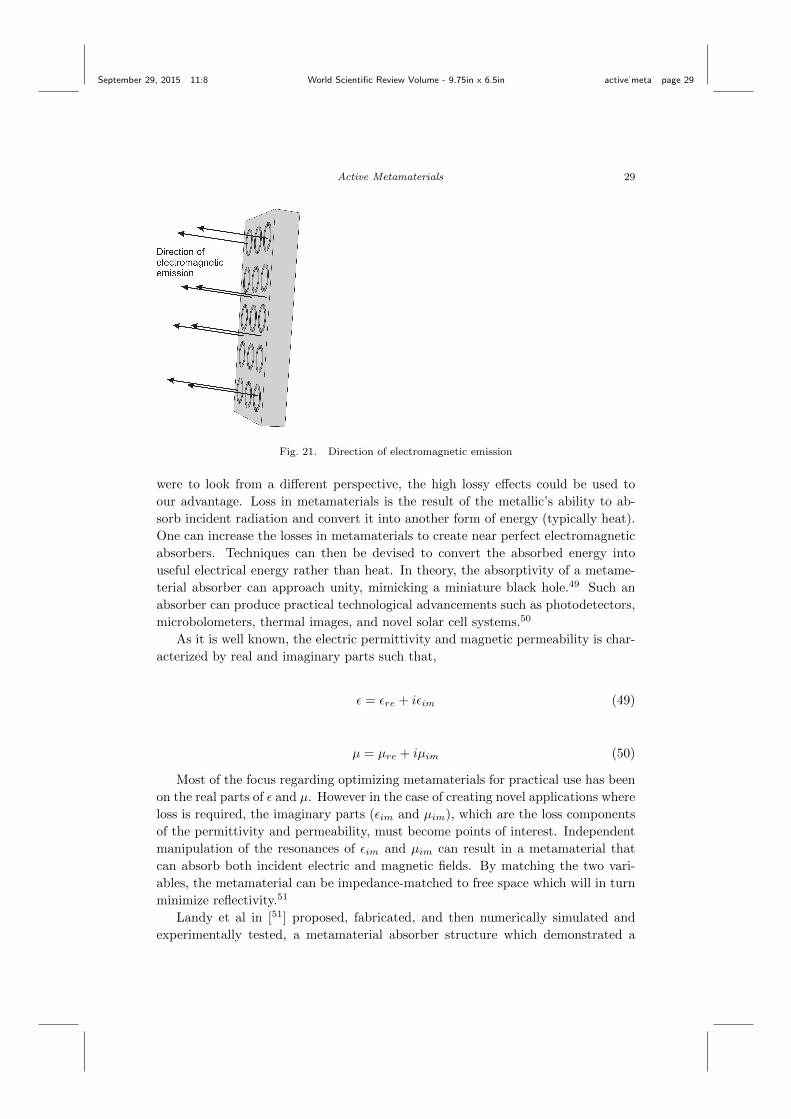
metamaterial array slab (see Fig. 21).
8. Moving in the Opposite Direction: Increasing Losses to Create
Metamaterial Absorbers
The inherent lossy effects of metallics that are used for metamaterial structures
severely plague metamaterial practicality in a plethora of ways. However, if one
September 29, 2015 11:8 World Scientific Review Volume - 9.75in x 6.5in active˙meta page 29
Active Metamaterials 29
Fig. 21. Direction of electromagnetic emission
were to look from a different perspective, the high lossy effects could be used to
our advantage. Loss in metamaterials is the result of the metallic’s ability to ab-
sorb incident radiation and convert it into another form of energy (typically heat).
One can increase the losses in metamaterials to create near perfect electromagnetic
absorbers. Techniques can then be devised to convert the absorbed energy into
useful electrical energy rather than heat. In theory, the absorptivity of a metame-
terial absorber can approach unity, mimicking a miniature black hole.49 Such an
absorber can produce practical technological advancements such as photodetectors,
microbolometers, thermal images, and novel solar cell systems.50
As it is well known, the electric permittivity and magnetic permeability is char-
acterized by real and imaginary parts such that,
ε = εre + iεim (49)
µ = µre + iµim (50)
Most of the focus regarding optimizing metamaterials for practical use has been
on the real parts of ε and µ. However in the case of creating novel applications where
loss is required, the imaginary parts (εim and µim), which are the loss components
of the permittivity and permeability, must become points of interest. Independent
manipulation of the resonances of εim and µim can result in a metamaterial that
can absorb both incident electric and magnetic fields. By matching the two vari-
ables, the metamaterial can be impedance-matched to free space which will in turn
minimize reflectivity.51
Landy et al in [51] proposed, fabricated, and then numerically simulated and
experimentally tested, a metamaterial absorber structure which demonstrated a
September 29, 2015 11:8 World Scientific Review Volume - 9.75in x 6.5in active˙meta page 30
30 Michael D. Singh and Marek S. Wartak
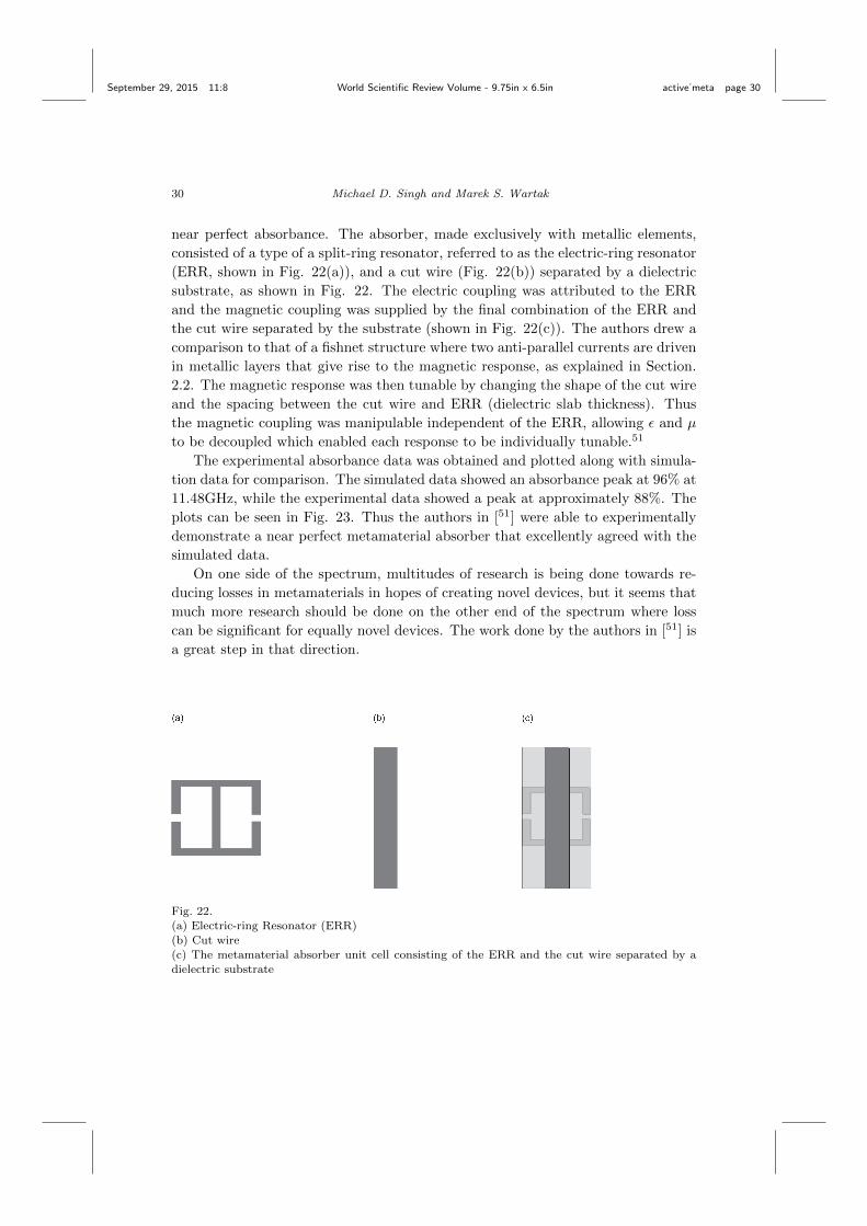
near perfect absorbance. The absorber, made exclusively with metallic elements,
consisted of a type of a split-ring resonator, referred to as the electric-ring resonator
(ERR, shown in Fig. 22(a)), and a cut wire (Fig. 22(b)) separated by a dielectric
substrate, as shown in Fig. 22. The electric coupling was attributed to the ERR
and the magnetic coupling was supplied by the final combination of the ERR and
the cut wire separated by the substrate (shown in Fig. 22(c)). The authors drew a
comparison to that of a fishnet structure where two anti-parallel currents are driven
in metallic layers that give rise to the magnetic response, as explained in Section.
2.2. The magnetic response was then tunable by changing the shape of the cut wire
and the spacing between the cut wire and ERR (dielectric slab thickness). Thus
the magnetic coupling was manipulable independent of the ERR, allowing ε and µ
to be decoupled which enabled each response to be individually tunable.51
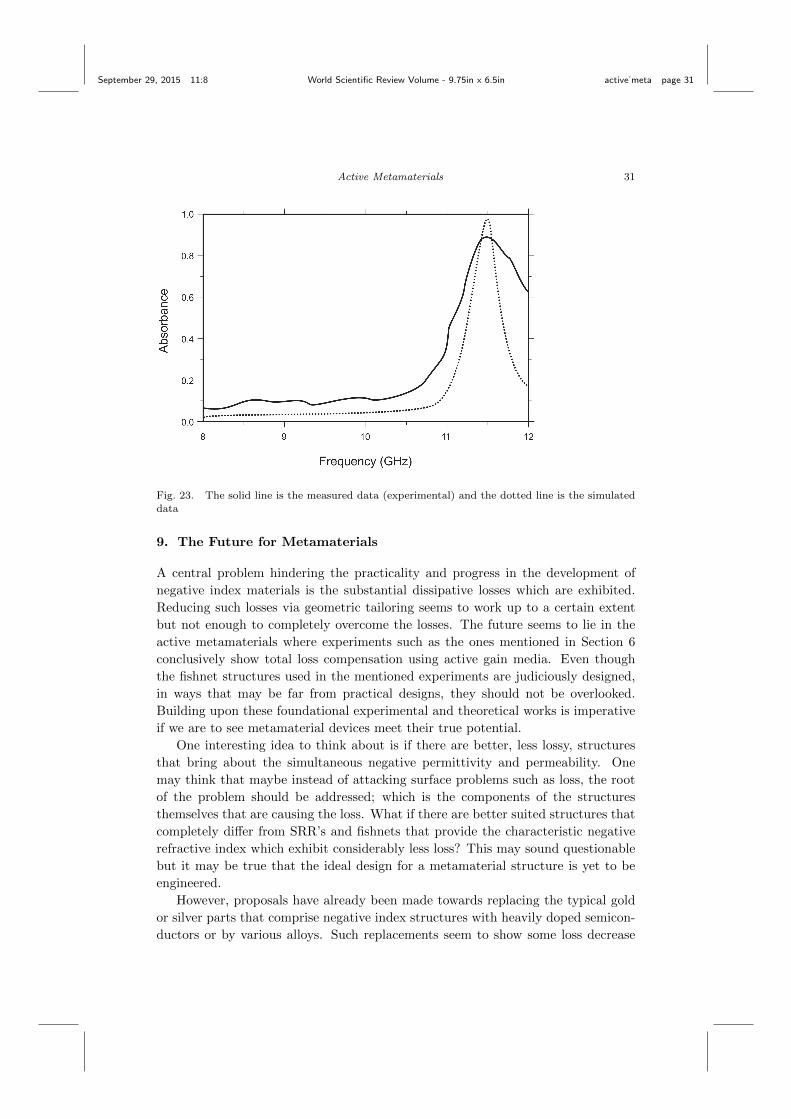
The experimental absorbance data was obtained and plotted along with simula-
tion data for comparison. The simulated data showed an absorbance peak at 96% at
11.48GHz, while the experimental data showed a peak at approximately 88%. The
plots can be seen in Fig. 23. Thus the authors in [51] were able to experimentally
demonstrate a near perfect metamaterial absorber that excellently agreed with the
simulated data.
On one side of the spectrum, multitudes of research is being done towards re-
ducing losses in metamaterials in hopes of creating novel devices, but it seems that
much more research should be done on the other end of the spectrum where loss
can be significant for equally novel devices. The work done by the authors in [51] is
a great step in that direction.
Fig. 22.
(a) Electric-ring Resonator (ERR)(b) Cut wire
(c) The metamaterial absorber unit cell consisting of the ERR and the cut wire separated by adielectric substrate
September 29, 2015 11:8 World Scientific Review Volume - 9.75in x 6.5in active˙meta page 31
Active Metamaterials 31
Fig. 23. The solid line is the measured data (experimental) and the dotted line is the simulated
data
9. The Future for Metamaterials
A central problem hindering the practicality and progress in the development of
negative index materials is the substantial dissipative losses which are exhibited.
Reducing such losses via geometric tailoring seems to work up to a certain extent
but not enough to completely overcome the losses. The future seems to lie in the
active metamaterials where experiments such as the ones mentioned in Section 6
conclusively show total loss compensation using active gain media. Even though
the fishnet structures used in the mentioned experiments are judiciously designed,
in ways that may be far from practical designs, they should not be overlooked.
Building upon these foundational experimental and theoretical works is imperative
if we are to see metamaterial devices meet their true potential.
One interesting idea to think about is if there are better, less lossy, structures
that bring about the simultaneous negative permittivity and permeability. One
may think that maybe instead of attacking surface problems such as loss, the root
of the problem should be addressed; which is the components of the structures
themselves that are causing the loss. What if there are better suited structures that
completely differ from SRR’s and fishnets that provide the characteristic negative
refractive index which exhibit considerably less loss? This may sound questionable
but it may be true that the ideal design for a metamaterial structure is yet to be
engineered.
However, proposals have already been made towards replacing the typical gold
or silver parts that comprise negative index structures with heavily doped semicon-
ductors or by various alloys. Such replacements seem to show some loss decrease
September 29, 2015 11:8 World Scientific Review Volume - 9.75in x 6.5in active˙meta page 32
32 Michael D. Singh and Marek S. Wartak
but need to be examined further. Another proposal considers an all-dielectric meta-
material that also showed better loss performance.45
Metamaterials display tremendous potential with a promise to advance numer-
ous technologies beyond our imagination. Fascination of metamaterials within the
scientific community will continue at its fast pace until these technologies are actu-
alized. The remarkable growth of attention this field has received and continues to
receive ensures a very bright future for metamaterials.
Acknowledgment
The authors acknowledge financial support from the Natural Sciences and En-
gineering Research Council of Canada (NSERC).
References
1. Y. Liu and X. Zhang, Metamaterials: a new frontier of science and technology, Chem-ical Society Reviews. 40(5), 2494–2507, (2011).
2. P. Kinsler and M. W. McCall, Criteria for negative refraction in active and passivemedia, Microwave and Optical Technology Letters. 50, 1804–1807, (2008).
3. S. Ramakrishna and T. Grzegorczyk, Physics and Applications of Negative RefractiveIndex Materials. (SPIE Press and CRC Press, Bellingham, Washington, USA, 2009).
4. J. Pendry, Negative refraction makes a perfect lens, Phys. Rev. Lett. 85(18), 3966,(2000).
5. U. Leonhardt, Optical conformal mapping, Science. 312(5781), 1777–1780, (2006).6. D. Schurig, J. Mock, B. Justice, S. Cummer, J. Pendry, A. Starr, and D. Smith,
Metamaterial electromagnetic cloak at microwave frequencies, Science. 314(5801),977–980, (2006).
7. K. Tsakmakidis, A. Boardman, and O. Hess, Trapped rainbow storage of light inmetamaterials, Nature. 450(7168), 397–401, (2007).
8. S. O’Brien, D. McPeake, S. Ramakrishna, and J. Pendry, Near-infrared photonic bandgaps and nonlinear effects in negative magnetic metamaterials, Phys. Rev. B. 69(24),241101, (2004).
9. V. Shalaev, Optical negative-index metamaterials, Nature Photonics. 1, 41–48, (2007).10. C. Hafner, C. Xudong, and R. Vahldieck, Resolution of negative-index slabs, J. Opt.
Soc. Am. A. 23(7), 1768–1778, (2006).11. M. Stockman, Criterion for negative refraction with low optical losses from a funda-
mental principle of causality, Phys. Rev. Lett. 98, 177404, (2007).12. K. Webb and L. Thylen, Perfect-lens-material condition from adjacent absorptive and
gain resonances, Optics Letters. 33(7), 747–749, (2008).13. A. Bratkovsky, E. Ponizovskaya, S. Wang, Y. F. P. Holmstrom, L. Thylen, and
H. Agren, A metal-wire/quantum-dot composite metamaterial with negative ε andcompensated optical loss, Appl. Phys. Let. 93, 193106, (2008).
14. M. Wegener, J. GarcYa-Pomar, C. Soukoulis, N. Meinzer, M. Ruther, and S. Linden,Toy model for plasmonic metamaterial resonances coupled to two-level system gain,Optics Express. 16(24), 19785–19798, (2008).
15. A. Fang, T. Koschny, M. Wegener, and C. Soukoulis, Self-consistent calculation ofmetamaterials with gain, Phys. Rev. B. 79(24), 241104, (2009).
September 29, 2015 11:8 World Scientific Review Volume - 9.75in x 6.5in active˙meta page 33
Active Metamaterials 33
16. Y. Yuan, B. Popa, and S. Cummer, Zero loss magnetic metamaterials using poweredactive unit cells, Optics Express. 17(18), 16135–16143, (2009).
17. Y. Sivan, S. Xiao, U. Chettiar, A. Kildishev, and V. Shalaev, Frequency-domainsimulations of a negative-index material with embedded gain, Optics Express. 17(26),24060–24074, (2009).
18. V. Veselago, The electrodynamics of substances, Sov. Phys. Usp. 10(4), 509–514,(1968).
19. J. Pendry, A. Holden, D. Robbins, and W. Stewart, Magnetism from conductors andenhanced nonlinear phenomena, IEEE Trans. Microw. Theory Tech. 47(11), 2075–2084, (1999).
20. W. Zaoui, K. Chen, W. Vogel, and M. Berroth, Low loss broadband polarizationindependent fishnet negative index metamaterial at 40GHz, Photonics and Nanos-tructures: Fundamentals and Applications. 10(3), 245–250, (2012).
21. D. Smith, W. Padilla, D. Vier, S. Nemat-Nasser, and S. Schultz, Composite mediumwith simultaneously negative permeability and permittivity, Phys. Rev. Lett. 84(18),4184, (2000).
22. N. Dutta, I. Mirza, S. Shi, and D. Prather, Fabrication of large area fishnet opticalmetamaterial structures operational at near-IR wavelengths, Materials. 3(12), 5283–5292, (2010).
23. M. Kafesaki, I. Tsiapa, N. Katsarakis, T. Koschny, C. Soukoulis, and E. Economou,Left-handed metamaterials: The fishnet structure and its variations, Phys. Rev. B.75(23), 235114, (2007).
24. J. Pendry, D. Schurig, and D. Smith, Controlling electromagnetic fields, Science. 312(5781), 1780–1782, (2006).
25. J. Khurgin and G. Sun, In search of the elusive lossless metal, Appl. Phys. Let. 96(18), 181102, (2010).
26. J. Khurgin and G. Sun, Scaling of losses with size and wavelength in nanoplasmonicsand metamaterials, Appl. Phys. Let. 99(21), 211106, (2011).
27. J. Khurgin, How to deal with the loss in plasmonics and metamaterials, Nature Nan-otechnology. 10(1), 2–6, (2015).
28. A. Fang, T. Koschny, and C. Soukoulis, Lasing in metamaterial nanostructures, Jour-nal of Optics. 12(2), 024013, (2010).
29. J. Khurgin and G. Sun, Practicality of compensating the loss in the plasmonic waveg-uides using semiconductor gain medium, Appl. Phys. Let. 100(1), 011105, (2012).
30. G. Dolling, M. Wegener, C. Soukoulis, and S. Linden, Design-related losses of double-fishnet negative-index photonic metamaterials, Optics Express. 15(18), 11536–11541,(2007).
31. G. Dolling, C. Enkrich, M. Wegener, C. Soukoulis, and S. Linden, Low-loss negative-index metamaterial at telecommunication wavelengths, Optics Letters. 31(12), 1800–1802, (2006).
32. D. Guney, T. Koschny, and C. Soukoulis, Reducing ohmic losses in metamaterials bygeometric tailoring, Phys. Rev. B. 80(12), 125129, (2009).
33. J. Zhou, T. Koschny, and C. Soukoulis, An efficient way to reduce losses of left-handedmetamaterials, Optics Express. 16(15), 11147–11152, (2008).
34. A. Popov and V. Shalaev, Compensating losses in negative-index metamaterials byoptical parametric amplification, Optics Letters. 31(14), 2169–2171, (2006).
35. S. Xiao, V. Drachev, A. Kildishev, X. Ni, U. Chettiar, H. Yuan, and V. Shalaev, Loss-free and active optical negative-index metamaterials, Nature. 466(7307), 735–738,(2010).
36. E. Plum, V. Fedotov, P. Kuo, D. Tsai, and N. Zheludev, Towards the lasing spacer
September 29, 2015 11:8 World Scientific Review Volume - 9.75in x 6.5in active˙meta page 34
37. K. Tanaka, E. Plum, J. Ou, T. Uchino, and N. Zheludev, Multifold enhancement ofquantum dot luminescence in plasmonic metamaterials, Phys. Rev. Lett. 105, 227403,(2010).
38. N. Meinzer, M. Ruther, S. Linden, C. M. Soukoulis, G. Khitrova, J. Hendrickson,J. Olitzky, H. Gibbs, and M. Wegener, Arrays of ag split-ring resonators coupled toingaas single-quantum-well gain, Optics Express. 18, 24140, (2010).
39. N. Meinzer, M. Konig, M. Ruther, S. Linden, G. Khitrova, H. Gibbs, K. Busch, andM. Wegener, Distance-dependence of the coupling between split-ring resonators andsingle-quantum-well gain, Appl. Phys. Let. 99, 111104, (2011).
40. S. Wuestner, A. Pusch, K. Tsakmakidis, J. Hamm, and O. Hess, Overcoming losseswith gain in a negative refractive index metamaterial, Phys. Rev. Lett. 105(12),127401, (2010).
41. Z. Huang, S. Droulias, T. Koschny, and C. M. Soukoulis, Mechanism of the metallicmetamaterials coupled to the gain material, Optics Express. 22, 28596, (2014).
42. A. Pusch, S. Wuestner, J. Hamm, K. Tsakmakidis, and O. Hess, Coherent amplifi-cation and noise in gain-enhanced nanoplasmonic metamaterials: a Maxwell-BlochLangevin approach, ACS NANO. 6, 2420–2431, (2012).
43. S. Wuestner, A. Pusch, K. Tsakmakidis, J. Hamm, and O. Hess, Gain and plasmondynamics in active negative-index metamaterials, Phil. Trans. R. Soc. A. 369, 3523–3550, (2011).
44. B.-I. Popa and S. Cummer, An architecture for active metamaterial particles andexperimental validation at rf, Microwave and Optical Technology Letters. 49(10),2574–2577, (2007).
45. S. Wuestner and O. Hess, Active optical metamaterials, PROGRESS IN OPTICS,VOL 59. 59, 1–88, (2014).
46. M. Stockman, Spasers explained, Nature Photonics. 2(6), 327–329, (2008).47. N. Zheludev, S. Prosvirnin, N. Papasimakis, and V. Fedotov, Lasing spaser, Nature
Photonics. 2(6), 351–354, (2008).48. V. Fedotov, M. Rose, S. Prosvirnin, N. Papasimakis, and N. Zheludev, Sharp trapped-
mode resonances in planar metamaterials with a broken structural symmetry, Phys.Rev. Lett. 99(14), 147401, (2007).
49. H. Chen, R. Miao, and M. Li, Transformation optics that mimics the system outsidea schwarzschild black hole, Optics Express. 18(14), 15183–15188, (2010).
50. J. Hao, L. Zhou, and M. Qiu, Nearly total absorption of light and heat generation byplasmonic metamaterials, Phys. Rev. B. 83(16), 165107, (2011).
51. N. Landy, S. Sajuyigbe, J. Mock, D. Smith, and W. Padilla, Perfect metamaterialabsorber, Phys. Rev. Lett. 100(20), 207402, (2008).
September 29, 2015 11:8 World Scientific Review Volume - 9.75in x 6.5in active˙meta page 35