Active Stabilization of the Magnetic Sensitivity in CMOS Hall Sensors Samuel Huber Lindenberger Dissertation zur Erlangung des Doktorgrades der Technischen Fakultät der Albert-Ludwigs-Universität Freiburg i. Br.
Transcript
Active Stabilization of the MagneticSensitivity in CMOS Hall Sensors
Samuel Huber Lindenberger
Dissertation zur Erlangung des Doktorgradesder Technischen Fakultät
der Albert-Ludwigs-Universität Freiburg i. Br.
Examiner: Prof. Dr. Oliver PaulCo-Examiner: Prof. Dr. Erik Thomsen
Dean: Prof. Dr. Oliver PaulDate of examination: 16 January 2017
Microsystem Materials Laboratory (Prof. Dr. O. Paul)Department of Microsystems Engineering – IMTEKUniversity of FreiburgFreiburg, Germany
Hall sensors are widely applied as magnetometers, position sensors, andcurrent sensors in countless automotive, industrial, and consumer prod-ucts. Unfortunately, the sensitivity of integrated CMOS Hall sensors isaffected by the influence of temperature and mechanical stress leading to asignificant reduction of the accuracy and hence limiting their scope. In con-ventional Hall sensors the temperature-related changes are compensatedusing a co-integrated temperature sensor. However, due to the piezo-Halland piezoresistance effects, conventional Hall sensors are prone to mechan-ical stress caused by the encapsulation into molded plastic packages andvarying environmental conditions. In consequence, the sensitivity remainsstress-dependent.
This thesis, in contrast, reports on integrated Hall sensors with an activestabilization of the magnetic sensitivity against both temperature and me-chanical stress. For the intended compensation of the parasitic effects,sensor elements and methods to measure the temperature and the relevantmechanical stress components were developed in a first step. They areboth realized as Wheatstone bridges formed by standard CMOS resistorsconnected to orthogonal pairs to obtain the desired isotropic sensitivitywith respect to the in-plane normal stresses. Thereafter, these sensor el-ements were integrated into Hall sensor microsystems with analog anddigital signal processing chains providing a temperature and stress com-pensated output. When packaged devices were exposed to temperaturesbetween −40 C and +120 C in the humid and dry package states, the Hallsensor microsystem with the analog signal processing was able to lowerthe temperature-related sensitivity changes of nearly 3% to below 0.5%whereas the stress-related changes of up to 1.6% were reduced to residual
7
Abstract
sensitivity errors smaller than 0.6%. Similarly, for the Hall sensor mi-crosystem with the digital signal processing chain the temperature-relatedsensitivity changes in the order of 40% as well as the stress-related changesreaching values of 2.6% were decreased to residual sensitivity errors below0.4%.
In conclusion, the novel, fully integrated Hall sensor microsystems allow tocontactlessly sense the magnetic field, position, or electric current with con-siderably higher accuracy than conventional Hall sensors. This is particu-larly relevant for applications in hybrid and electric vehicles, autonomousdriving, smart meters, power inverters, and many more. Moreover, thegenerality of the compensation approach makes the sensors independentfrom the surrounding such as their encapsulation at module level and fromthe varying environmental conditions.
8
Zusammenfassung
Hall-Sensoren werden in unzähligen Produkten zur Messung von Magnet-feldern, Position und elektrischem Strom verwendet. Die Empfindlichkeitvon Hall-Sensoren wird leider durch die Einflüsse von Temperatur undmechanischen Spannungen beeinträchtigt. Dies führt zu einer Reduktionihrer Genauigkeit und schränkt folglich ihr Anwendungsgebiet ein. Kon-ventionelle Hall-Sensoren benutzen einen ko-integrierten Temperatursen-sor, um die temperaturbedingten Änderungen zu kompensieren. Aufgrunddes Piezo-Hall-Effektes und des piezoresistiven Effektes sind konventionelleHall-Sensoren jedoch anfällig auf mechanische Spannungen, welche durchdie Verpackung und durch veränderliche Umweltbedingungen verursachtwerden. Ihre Empfindlichkeit bleibt deshalb abhängig von mechanischenSpannungen.
In der vorliegenden Arbeit werden integrierte Hall-Sensoren vorgestellt,deren magnetische Empfindlichkeit aktiv stabilisiert wird gegenüber denEinflüssen von Temperatur und mechanischen Spannungen. Für die beab-sichtigte Kompensation dieser parasitären Effekte wurden in einem erstenSchritt geeignete Sensorelemente und Methoden zur Messung der Tempe-ratur und der relevanten Spannungskomponenten entwickelt. Beide Sen-sorelemente sind Wheatstone’sche Brückenschaltungen. Sie bestehen ausStandard CMOS Widerständen, welche zu orthogonalen Paaren zusam-mengeschaltet sind. Auf diese Weise erhalten sie die erwünschte isotropeEmpfindlichkeit gegenüber den Normalspannungen in der Ebene. Danachwurden die Sensorelemente in zwei Hall-Sensor-Mikrosysteme mit analogersowie digitaler Signalverarbeitung integriert. Beide Sensor-Mikrosystemeliefern gegenüber parasitären Einflüssen kompensierte Ausgangssignale.Verpackte Sensor-Mikrosysteme wurden Temperaturen zwischen −40 C
9
Zusammenfassung
und +120 C ausgesetzt, sowohl im feuchten als auch im trockenen Zu-stand der Verpackung. Das Hall-Sensor-Mikrosystem mit analoger Signal-verarbeitung war imstande, temperaturbedingte Empfindlichkeitsänderun-gen von nahezu 3% auf unter 0.5% zu verringern. Gleichzeitig wurde diedurch mechanische Spannungen hervorgerufene Änderung der Empfind-lichkeit von 1.6% auf unter 0.6% reduziert. Beim Hall-Sensor-Mikrosystemmit digitaler Signalverarbeitung lagen die durch Temperatur und mechani-sche Spannungen verursachten Empfindlichkeitsänderungen bei 40% bezie-hungsweise 2.6%. Beide Einflüsse konnten nach erfolgter Kompensation aufRestfehler der magnetischen Empfindlichkeit unter 0.4% verringert werden.
Zusammenfassend erlauben die neuen, vollintegrierten Hall-Sensor-Mikro-systeme die kontaktlose Messung von Magnetfeldern, Position und elektri-schem Strom mit signifikant höherer Genauigkeit als konventionelle Hall-Sensoren. Dies ist insbesondere relevant für hybride und elektrische An-triebssysteme, autonomes Fahren, intelligente Stromzähler, Frequenzum-richter u.v.m. Darüber hinaus erreicht die Allgemeingültigkeit des Kom-pensationsansatzes sowohl die Unabhängigkeit gegenüber der Art der Ver-packung als auch der beliebigen Umweltbedingungen.
10
Chapter 1
Introduction
1.1 Hall Sensors for Contactless Position and Cur-rent Measurement
CMOS integrated Hall sensors are widely used as magnetometers, posi-tion sensors, and current sensors in consumer, industrial, and automotiveproducts. Examples of commercial Hall sensor applications include abso-lute rotary position sensing, three-axis position sensing, gear wheel positionand speed sensing, conventional open-loop or closed-loop current sensing,planar current sensing, and linear position sensing. These applications areillustrated in Figs. 1.1 (a)-(f).
Used as magnetic field sensors, silicon Hall devices have been demonstratedto sense magnetic fields between roughly 10 T and 10−4 T [1]. Naturally,planar Hall plates are sensitive to the out-of-plane magnetic field com-ponent, whereas the in-plane components become accessible with verticalHall devices [2]. However, complemented with integrated magnetic concen-trators, planar Hall sensors can be used to measure all three componentsof the magnetic field in a spot as small as 200µm× 200µm [3,4]. Further-more, magnetic fields down to the micro-Tesla range become accessible,enabling applications such as an electronic compass by directly measuringthe earth magnetic field [5, 6].
11
Chapter 1 Introduction
(a) (b) (c)
(d) (e) (f)
Figure 1.1: Hall sensors in action. (a) absolute rotary position sensor; (b)joystick sensor; (c) gear wheel sensor; (d) conventional contactless current sensorwith a ferromagnetic core; (e) planar contactless current sensor; (f) linear positionsensor. The illustrations are provided by Melexis.
1.2 Challenges of CMOS Integrated Hall Sensors
The performance of silicon Hall sensors is compromised by the harsh envi-ronmental conditions in which the devices are used. The operation temper-ature not uncommonly varies within −50 C and +175 C. Additionally,the devices are exposed to (i) thermal shocks, e. g., during the reflow solder-ing reaching a peak temperature of 260 C, (ii) a level of relative humiditybetween 0% and 100%, and (iii) mechanical stress in the order of severalhundred MPa.
On the other hand the Hall effect devices are sensitive not only to themagnetic field but also to radiation, temperature, and mechanical stress.Therefore the question arises how the parasitic influences originating fromthe environmental conditions are eliminated from the essential parameters
12
1.2 Challenges of CMOS Integrated Hall Sensors
of the Hall device used as a magnetic field transducer, i. e., sensitivity,offset, and linearity.The non-linearity of silicon integrated Hall plates is negligible in practicalposition and current sensor solutions considering magnetic fields up to200mT [7]. For Hall sensors with integrated ferromagnetic concentratorsthe linearity and hysteresis are highly relevant design parameters [8]. Theirtreatment would go beyond the scope of this text. Radiation is effectivelyeliminated by encapsulating the Hall sensor into a molded plastic packagewhich, on the other hand, exerts mechanical stress on the silicon. Thus,offset and sensitivity both as a function of temperature and mechanicalstress are left as a challenge.
Offset The impact of mechanical stress on the offset of Hall elementshas been studied by several research groups [9–12]. In general the methodof current spinning or orthogonal current switching [13] effectively elimi-nates the offset of a Hall plate even in cross-combination with temperature,mechanical stress, and the junction field effect [12]. Therefore orthogonalcurrent switching has been established as the de facto standard for the Hallsensor read-out. In practical Hall sensors with their many trade-offs withrespect to speed, power consumption, etc. the method of current spinningalone may not be sufficient. The remaining or residual offset is usually com-pensated against temperature, making use of an integrated temperaturesensor in combination with the necessary electronic circuitry. To my bestknowledge there is no Hall sensor available in which the cross-sensitivityof the residual offset with respect to mechanical stress is compensated.
Sensitivity The impact of a temperature change on the magnetic sensi-tivity is compensated with an integrated temperature sensor and the ap-propriate circuitry, which has been the state-of-the-art solution in the past.On the other hand the impact of mechanical stress on the sensitivity of aHall sensor is twofold. First the piezo-Hall effect [14] or the combination ofthe piezo-Hall and piezoresistance [15] effects lead to a relative change ofthe magnetic sensitivity, depending on whether the Hall plate is suppliedwith a constant current or a constant voltage, respectively. Secondly, ifthe thermal change of the sensitivity is compensated with an integratedtemperature sensor, the cross-sensitivity of the temperature sensor withrespect to mechanical stress additionally degrades the accuracy of the Hall
13
Chapter 1 Introduction
sensor. In summary, modern integrated silicon Hall sensors suffer from thecross-sensitivity of their magnetic sensitivity with respect to mechanicalstress.
1.2.1 Mechanical Stress
Integrated circuits are exposed to mechanical stress for many reasons:stress can be caused by the wafer fabrication process, by the packagingmaterials, in particular plastic components, by the soldering of the pack-age onto a printed circuit board, by overmolding processes to form a plasticencapsulated module, by external forces such as hydrostatic pressure andmounting constraints, and many more reasons. Mechanical stress exertedfrom the encapsulation of the silicon chip into a molded plastic package isthe most common cause of mechanical stress in integrated circuits.
Package Stress under Environmental Conditions The encapsula-tion stress however is not constant but changes under the variation of theenvironmental conditions. Consequently, the change of package-inducedstress is particularly relevant for Hall sensors [16–19]. The stress changehas three main causes:
1. Temperature variations combined with different thermal expansioncoefficients of the involved materials lead to variable, temperature-dependent mechanical stress, i. e., the thermo-elastic stress as intro-duced in Section 2.6.
2. The absorption of moisture by the mold compound is responsible forthe swelling of the polymer. At room temperature a time constantof about 240 hours has been documented for the humidity soaking ofa dry package [18,19].
3. The long-term change of mechanical stress [16] and material proper-ties [20] due, e. g., to material relaxation and continuing polymeriza-tion of the mold compound with age.
The purely thermo-elastic contribution can be compensated by using anintegrated temperature sensor in combination with the compensation cir-cuitry. Clearly this method is able to provide a stable, reliable solution
14
1.3 Stabilization of the Hall Magnetic Sensitivity
only if the thermo-mechanical properties of the package materials do notchange during the device lifetime.
However, material properties do vary with temperature as well as time[16,17]. Furthermore, when undergoing thermal cycling, sensor packagingmaterials experience visco-elastic and possibly even plastic deformations.This leads to stress hysteresis in the sensor output with temperature vari-ation [20].
Finally, the moisture absorption by the package mold compound has beenfound to cause significant stress changes in packages [21] and to thus alterthe sensitivity of packaged Hall sensors [18, 19]. For a change of relativehumidity from 0% to 90%, a corresponding maximum change of the mag-netic sensitivity of 2.7% has been reported [19]. Similarly for a change ofrelative humidity from 0% to 100% a corresponding maximum change ofthe magnetic sensitivity between 2% and 6% has been reported for threedifferent mold compounds [18].
In conclusion, the compensation of this cross-sensitivity is inevitable forHall sensors used for measuring the absolute magnetic field such as mag-netometers, open-loop current sensors, and position sensors. Hence thefollowing section introduces ways to eliminate the parasitic effects result-ing in a stabilization of the magnetic sensitivity.
1.3 Stabilization of the Hall Magnetic Sensitivity
The elimination of the parasitic sensitivity change related to temperatureand mechanical stress may be done for a conventional integrated Hall sen-sor with a temperature sensor in combination with an optimized packagingprocess [22] or by etching the Hall device free from the bulk silicon [23].Another possibility is to actively compensate by dedicated circuitry whichis the scope of this work. A variety of possibilities with implementationin analog or digital circuitry as well as from system level down to devicelevel are imaginable. The temperature and mechanical stress can be mea-sured with dedicated means, followed by the digitization and a subsequentcompensation in the digital domain [24, 25]. With the help of a referencemagnetic field the magnetic sensitivity can be extracted. A correspondinggain adjustment leads to a continuous sensitivity calibration [26–28] which
15
Chapter 1 Introduction
even does not necessitate temperature and stress measurements. The sup-ply current of the Hall plate may be dependent on temperature and me-chanical stress leading to a circuit level implementation fully compatiblewith analog circuitry. Another method implementable in analog circuitryis a variable gain of the amplification chain at the output of the Hall plate,whereby the gain depends on mechanical stress and temperature. Further-more it is possible to implement the temperature and stress compensationdirectly at device level by, e. g., controlling the common mode potential ofthe Hall plate leading to a sensitivity modulation making use of the junc-tion field effect [29], or by controlling the sensitivity of the Hall plate viathe gate voltage of a MOS-type device. These possibilities are summarizedin Figs. 1.2 (a)-(f).
1.4 Scope and Outline of the Thesis
The scope of this thesis is to stabilize the magnetic sensitivity of CMOSintegrated planar Hall sensors with respect to temperature and mechanicalstress by the use of co-integrated temperature and stress sensors and thenecessary circuitry. Therefore, in a first step, sensor elements for the on-chip measurement of temperature and mechanical stress are developed.In a second step these sensors are used to build integrated Hall sensormicrosystems with temperature and stress compensation. Thereby the goalis to provide solutions which are independent from the source of mechanicalstress. In that way the same solution remains valid for different typesof molded plastic packages, e. g., single-in-line, SOIC-8, and TSSOP-16packages.
In Chapter 2 the fundamentals of CMOS silicon integrated Hall sensors andtheir parasitic effects relevant for this thesis are introduced. The chapteris completed with a section on numerical modeling of package-inducedmechanical stress. The experimental methods developed for this work arepresented in Chapter 3. The parasitic cross-sensitivities of Hall sensors toboth temperature and stress necessitate the experimental validation withrespect to mechanical stress without temperature, temperature withoutmechanical stress, and the combination of temperature and mechanicalstress.
The sensor elements and methods for the on-chip measurement of me-
16
1.4 Scope and Outline of the Thesis
A/DT
σ
μC
HBref ∝ Icoil
gaincontrol
gate
channel
SI, SV = f(Vgate)
Gain = f(T, σ)
T σ
SI = f(Vmid)
t
Vmid = Vref
Iplate = f(T, σ)
(a) (b)
(c) (d)
(e) (f)
V(T, σ)
R(T, σ)
Figure 1.2: Active compensation of the sensitivity change in planar Hall sensors.(a) Hall sensor microsystem with a digital signal processing chain and additionalmeans to measure the temperature and mechanical stress. The compensation isrealized as a calculation in the microcontroller. (b) Hall sensor with a referencefield generator and a continuous gain calibration, e. g., [28]. (c) Control of thesensitivity via the Hall plate supply, e. g., the supply current [25]. (d) The variablegain is a function of the temperature or the mechanical stress. (e) Plate thicknessmodulation due to the junction field effect; the mid potential to GND, i. e., Vmidis controlled to be Vref [29]. (f) Depletion or inversion type MOS Hall device; thechannel thickness, the electron density, and the electron mobility are functions ofthe applied gate voltage.
17
Chapter 1 Introduction
chanical stress and temperature developed in the course of this thesis aredescribed and experimentally validated in Chapter 4. It includes a pack-age stress sensor, a temperature sensor, a combined stress and temperaturesensor, and a combined Hall and stress sensor.
Based on these sensor elements an analog as well as a digital Hall sensormicrosystem were developed and experimentally validated. Both of thesemicrosystems include a simultaneous temperature and stress compensationin order to maintain a constant magnetic sensitivity. The correspondingwork is summarized in Chapters 5 and 6, respectively. The thesis is con-cluded with Chapter 7.
18
Chapter 2
Fundamentals
2.1 The Hall Effect
Discovered in 1879 by Edwin Hall, his new action of the magnet on electriccurrents [30] is today called the Hall effect. It describes the appearanceof an electric field EH orthogonal to the drift velocity v of charge carriersdue to a current flow in a thin conductive sheet and to the magnetic fluxdensity B, i. e., [31]
EH ∝ v ×B . (2.1)
Thereby EH counterbalances the force that the moving charges experiencein the magnetic field. The charges move by their drift velocity, describedas the product of the externally applied electric field E and the mobilityof the charge carriers µ, i. e.,
v = µE . (2.2)
For the sake of generality µ is introduced here as a second rank tensorparticularly in view of the stress-related effects, i. e., piezoresistance effectwhich will be introduced in the course of this chapter. For unstressedsilicon the scalar value µ may be used.
19
Chapter 2 Fundamentals
A conventional Hall plate consists of a conductive sheet and four contactsC1 to C4. Two of the contacts (C1 and C3) on opposite sides are usedto drive current through the conductive sheet. On the other two contacts(C2 and C4) the differential Hall voltage VH is measured. It represents theintegral of (2.1) along the width W , i. e.,
VH =∫ r2
r1EH · dl , (2.3)
where r1 and r2 denote the positions of the two sensing contacts betweenwhich VH is measured. The appearance of the Hall effect in an n-typesemiconductor material is depicted in Fig. 2.1 by the example of a longrectangular plate.
B E
v
EH
C2
C3
C4
C1
x
y
z
VH
I
Lt
W
B E
v
E
Figure 2.1: The Hall effect as it appears in a rectangular plate of n-type material.
Thanks to the high mobility of their charge carriers, the Hall effect ismost prominent in semiconductors. The values of the electron mobility ofselected semiconductors are summarized in Table 2.1.Although silicon has a moderate electron mobility compared to other semi-conductors, it is today the major substrate for integrated Hall sensors.Thanks to the advantage of the complementary metal oxide semiconduc-tor (CMOS) technology the Hall devices are cointegrated together with
20
2.1 The Hall Effect
Table 2.1: Scalar values of the electron mobility µn of selected unstressed semi-conductors at 300K [32].
Material µn(cm2 V−1 s−1)
Si 1450Ge 3900
GaAs 8000InSb 80000
switches, amplifiers, and the like. In fact, the Hall device is merely oneavailable feature for magnetic field measurement in CMOS integrated cir-cuits [33]. However, it is readily available as n-well and can therefore besupplied with a positive voltage versus the p-type substrate. Furthermoreit features a differential output voltage around half the supply voltage andit can be scaled down to a few µm in size. A conventional planar Halldevice in CMOS technology consists of a conductive sheet made of n-wellmaterial and four n+ contacts with silicided surface. The n-well is coveredby a p+ layer in order to bury it underneath the surface, such that theelectron flow is not affected by the silicon-SiO2 interface. The active n+
and p+ regions are separated by the shallow trench isolation (STI). TheHall plate is surrounded by a substrate contact ring made of p-well andp+ material. A cross-section of a CMOS-compatible planar Hall plate issketched in Fig. 2.2.
2.1.1 Hall Coefficient and Hall Mobility
The Hall electric field (2.1) can be expressed in terms of the Hall coefficienttensor RH [34–36], i. e.,
EH = (RHB)× J , (2.4)
where J denotes the electric current density. For electrons in unstressedsilicon the scalar quantities of RH and the Hall mobility µH are given by [31]
RH = − rHqen
, (2.5)
21
Chapter 2 Fundamentals
p-epi substrate
p-wafer
Hall plate
substrate contact ring
Hallcontacts
STIn+
n-wellsilicidep+
p-wellp-epip-wafer
Figure 2.2: Schematic cross-section of a planar Hall plate in a CMOS process.The silicon oxide, metal layers, and passivation are omitted from the figure.
andµH = −rHµ , (2.6)
where rH, qe, and n denote the Hall scattering factor, the elementarycharge, and the electron density, respectively. The scalar value of the Hallscattering factor of electrons in unstressed silicon is approximately rH = 1.1at room temperature [31].
2.2 Hall Plate Supply and Magnetic Sensitivity
The absolute magnetic sensitivity of a planar Hall device or integratedplanar Hall sensor is usually defined as
SH = ∂VH∂B⊥
, (2.7)
where B⊥ denotes the out-of-plane component of B and is therefore per-pendicular to the chip surface. The absolute sensitivity depends on con-ditions at which the Hall plate is operated, i. e., the temperature, themechanical stress, and the supply.
22
2.2 Hall Plate Supply and Magnetic Sensitivity
In conventional Hall sensors, the Hall elements are supplied by either aconstant voltage or a constant current. The different supply types havedistinct properties and are therefore discussed separately in the following.
2.2.1 Constant Voltage Supply
A constant voltage Vbias is applied between two opposite contacts, e. g.,on C1 and C3 in Fig. 2.1. The resulting voltage-related sensitivity SV =SH/Vbias is found to be [37]
SV = µHGV , (2.8)
where GV denotes the geometry factor with respect to the voltage-relatedsensitivity. For the given Hall element shape and dimensions the parameterGV is constant, whereas µH changes with temperature and mechanicalstress.
2.2.2 Constant Current Supply
Supplying the Hall element with a constant current Ibias between two op-posite contacts, e. g., on C1 and C3 in Fig. 2.1 results in the current-relatedsensitivity SI = SH/Ibias defined by [31]
SI = rHqent
GI = RHtGI , (2.9)
where t and GI denote the thickness of the conductive sheet and the ge-ometry factor with respect to the current-related sensitivity, respectively.Alternatively, when expressed as a function of the sheet resistance, (2.9)yields [37]
SI = µHRGI . (2.10)In the majority of integrated Hall sensors one of the two supply contactsis pinned to a fixed potential, being either Vlow = 0V, or Vhigh = 3.3V.For the given Hall element geometry and a strongly extrinsic doping, nand GI are assumed constant. The Hall scattering factor and Hall coef-ficient depend on mechanical stress and temperature [31]. Additionally,the plate thickness of a conventional CMOS n-well Hall plate is, via thejunction field effect, a function of the supply potentials with respect to thep-type substrate potential. This property stimulated the development ofthe following, third supply type.
23
Chapter 2 Fundamentals
2.2.3 Symmetric Constant Current Supply
The symmetric supply is a refinement of the constant current supply withan additional regulation of the center potential ψmid of the Hall plate withrespect to the substrate potential ψsub, i. e., Vmid = ψmid−ψsub, to a desiredreference Vref. In contrast to the conventional constant current supply noneof the supply contacts is pinned to a fixed potential [38]. Therefore thissupply concept is also called floating plate supply.
Via Vmid the plate thickness and therefore the current-related sensitiv-ity SI can be controlled to its desired values. Additionally, Vref may bea temperature-dependent and/or stress-dependent voltage and hence beused to compensate the undesired parasitic influences of temperature, me-chanical stress, and the junction field effect [29].
2.2.4 Relationship between Voltage-Related and Current-Related Sensitivities
The connection between the voltage-related sensitivity and the current-related sensitivity can be made via the supply bias resistance Rbias of theHall plate. In the special case of the plate depicted in Fig. 2.1 Rbias isgiven by
Rbias = ρL
Wt, (2.11)
where the electrical resistivity of the plate material is defined by
ρ = 1qenµ
= Rt . (2.12)
In the general case, the product of voltage-related sensitivity and plate biasresistance is readily found to be equivalent to the current-related sensitivity
SVRbias ≡ SI . (2.13)
As a consequence, the dimension-less geometrical factors are related viathe plate bias resistance and the sheet resistance [37], i. e.,
GVRbiasR
≡ GI . (2.14)
24
2.3 Piezoresistance Effect
2.2.5 Hall Supply Summary
In most cases CMOS Hall plates are optimized for maximum voltage-related sensitivity due to the inherent limitation of the maximum appli-cable voltage in modern CMOS circuitry, e. g., Vbias,max = 3.3 V. Even incase of constant current supply, applying Ohm’s law, the product of Ibiasand Rbias must not exceed Vbias,max. Consequently, the maximum absolutesensitivity can be written as
SH,max = Vbias,maxSV = Vbias,maxµHGV . (2.15)
Nevertheless, the advantage of the constant current supply is the relativelysmall change of the magnetic sensitivity with respect to the temperatureand the possibility to compensate for the undesired sensitivity to temper-ature and mechanical stress [39]. However, the current must be limitedto Ibias,max = Vbias,max/Rbias,max to ensure that the maximum applicablevoltage Vbias,max is not exceeded for the maximum Hall plate supply resis-tance Rbias,max, found at the highest applicable temperature. This resultsin a non-optimum sensitivity under more typical conditions, such as atroom temperature. On the other hand, with constant voltage supply theHall plate is always operated at the highest possible magnetic sensitivity(2.15), at the cost of a relatively large temperature-related change of themagnetic sensitivity.
2.3 Piezoresistance Effect
The change of the resistivity tensor elements with respect to mechanicalstress is known as piezoresistance effect [15,40,41], i. e.,
∆ρijρ0
=∑k,l
πijklσkl +O(σ2)
, (2.16)
where ρij , ρ0, πijkl, σkl, andO(σ2) denote the resistivity tensor, the stress-free resistivity, the 4th rank piezoresistance tensor, the 2nd rank tensor ofmechanical stress, and the nonlinear contribution to the piezoresistance,respectively. The nonlinear piezoresistance effects are negligible for stressesup to 100 MPa [42] and are expected to be less than 5% for stresses up to200 MPa [41].
25
Chapter 2 Fundamentals
Reduced Index Notation Due to the symmetry of the mechanicalstress tensor σkl with only six independent elements and the same prop-erty of the resistivity tensor ρij , the relationship of the first order termof (2.16) linking the resistivity change with the mechanical stress can beestablished alternatively by a 6× 6 matrix [43], i. e.,
1ρ0
∆ρ1
∆ρ2
∆ρ3
∆ρ4
∆ρ5
∆ρ6
=
π11 π12 π13 π14 π15 π16
π21 π22 π23 π24 π25 π26
π31 π32 π33 π34 π35 π36
π41 π42 π43 π44 π45 π46
π51 π52 π53 π54 π55 π56
π61 π62 π63 π64 π65 π66
σ1
σ2
σ3
σ4
σ5
σ6
, (2.17)
whereby in the original orientation of, e. g., the cubic silicon crystal, thenon-zero elements are π11 = π22 = π33, π12 = π21 = π13 = π31 = π23 = π32,and π44 = π55 = π66. Commonly the indices 1 to 6 are mapped to thetensor elements (chip coordinates) by 1→ 11(xx), 2→ 22(yy), 3→ 33(zz),4 → 23(yz), 5 → 13(xz), 6 → 12(xy). A summary of the piezoresistancecoefficients of n-type and p-type silicon is given in Table 2.2.
Table 2.2: Summary of piezoresistance coefficients of lightly doped silicon withrespect to the crystal coordinate system at 300K [15].
Material π11 π12 π44(GPa−1
) (GPa−1
) (GPa−1
)n-type −1.02 +0.53 +0.13p-type +0.06 −0.01 +1.38
As is evident from Table 2.2, the piezoresistance effect in silicon is highlyanisotropic, i. e., π11 − π12 6= π44. Besides its applicability for strain andtorque sensors, the piezoresistance effect is exploited in, e. g., MEMS pres-sure sensors [44].
26
2.3 Piezoresistance Effect
2.3.1 Piezoresistance for an Arbitrary Coordinate System
Expressions (2.16) and (2.17) are generally valid for any arbitrary deviceorientation. However, one has to carefully take into account the orienta-tion of the Si crystal and the mechanical stress for the following reasons:(i) standard CMOS wafers are not oriented along the original crystal axesof silicon, and (ii) integrated circuits, although rarely, can be cut fromthe wafer at any arbitrary orientation, not only in directions parallel andperpendicular with respect to the wafer flat.
Mechanical Stress Rotation For an arbitrary orientation of the me-chanical stress with respect to the integrated circuit one has to rotate thestress tensor σkl according to the rules of tensor transformation [40, 45],i. e.,
σij =∑k,l
MikMjlσkl , (2.18)
where M denotes the rotation matrix. When expressed in terms of Eu-ler angles with a first rotation around the vertical axis z by angle φ→ (x′, y′, z′), a second rotation around x′ by angle θ → (x′′, y′′, z′′), and athird rotation around z′′ by angle ψ the rotation matrix reads [40]
where c and s denote the cosine and sine functions, respectively. For therotation of the in-plane stresses around the vertical axis by angle φ andneglecting out-of-plane stresses, (2.19) reduces to
M =
cosφ − sinφsinφ cosφ
. (2.20)
The stress components in the new orientation are found to be
Hence, the sum of in-plane normal stresses σsum, i. e.,
σsum = σxx + σyy (2.24)
is an invariant under rotation. However, the difference of in-plane normalstresses σD, i. e.,
σD = σxx − σyy (2.25)
transforms into a shear stress σ′S upon rotation by φ = 45, i. e.,
σ′S = σx′y′ = σxx − σyy2 . (2.26)
Similarly, the shear stress σxy transforms into
σx′x′ − σy′y′ = −2σxy . (2.27)
Silicon Crystal Rotation If the silicon crystal is rotated, the piezore-sistance coefficients need to be adapted accordingly by means of tensortransformation rules [40]. For the 6 × 6 matrix of piezoresistance coeffi-cients (2.17) the transformation rule reads [43,46]
π′ = TπT−1 , (2.28)
where π′ and T denote the piezoresistance matrix in the new orientationand the transformation matrix. The transformation matrix reads [46]
T =
l2x m2x n2
x 2lxnx 2mxnx 2lxmx
l2y m2y n2
y 2lyny 2myny 2lymy
l2z m2z n2
z 2lznz 2mznz 2lzmz
lxlz mxmz nxnz lxnz + nxlz mxnz +mznx lxmz + lzmx
lylz mymz nynz lynz + nylz mynz +mzny lymz + lzmy
lxly mxmy nxny lxny + nxly mxny +mynx lxmy + lymx
,
(2.29)where li, mi, and ni denote the direction cosines cf. (2.19) [40, 43] of thenew orientation with respect to the original silicon crystal. In standard
28
2.3 Piezoresistance Effect
(100) CMOS silicon the wafer flat and hence the devices are aligned alongthe 〈110〉 crystal direction. Therefore the piezoresistance coefficients needto be transformed accordingly, in this case by a rotation of 45 aroundthe vertical axis. As a result of the transformation, the piezoresistancecoefficients for CMOS silicon are summarized in Table 2.3.
Table 2.3: Summary of piezoresistance coefficients of (100) CMOS silicon at300K. The wafer flat is oriented along 〈110〉. The values are calculated basedon Table 2.2 applying the rules of tensor transformation. Only the non-zerocoefficients are listed.
2.3.2 Piezoresistance as a Function of Temperature andDoping Level
The stress-dependence of the piezoresistors is a function of temperatureand the doping level. It is modeled via a doping-dependent and temperature-dependent factor Pπ (N,T ) [43], i. e.,
π (N,T ) = Pπ (N,T )π0 , (2.30)
where π0 is the piezoresistance coefficient at the reference temperature andthe reference doping level.
For silicon diffused resistors the temperature-dependence of the piezoresis-tance coefficients at numerous doping levels has been investigated [47,48].For the fixed doping levels of the well material N ≈ 1017 cm−3 and of the
29
Chapter 2 Fundamentals
highly doped diffused resistors N ≈ 1020 cm−3 the approximate values ofPπ have been extracted, according to
Pπ = Pπ,N[1 + TCπ∆T +O
(∆T 2
)], (2.31)
where Pπ,N , TCπ, and O(∆T 2) denote the factor of doping-dependentreduction of the piezoresistance coefficient at the reference temperature,the first order temperature coefficient, and the higher order terms in ∆T ,respectively. A summary of Pπ,N and TCπ is available in Table 2.4.
2.4 CMOS Silicon Piezoresistors
In this work the piezoresistance effect is used to design CMOS-based stresssensors with a sensitivity to a specific stress component. Although it ispossible in CMOS technology to implement vertical resistors as stress sen-sors [49,50], in the present work only in-plane resistors are used. Thereforein-plane resistors and orthogonal resistor pairs in CMOS silicon are intro-duced as building blocks in the following two sections.A variety of in-plane resistors is readily available in CMOS silicon. Theyare defined by their sheet resistance R = ρ/t and the ratio of L/W ,whereas the resistors are structured laterally by photolithography and pro-cess control ensures that R is within the specified limits. A drawback ofthe resistors implemented in silicon is their relatively large temperaturecoefficient of resistance (TCR) due to the temperature-dependent mobil-ity. For the temperature range of interest, the resistance is described as asecond-order function of the temperature, i. e.,
R = R0(1 + α∆T + β∆T 2
), (2.32)
where R0, α, β, and ∆T denote the resistance at the reference temperature,the first and the second order TCR, and the temperature change with re-spect to the reference temperature, i. e., T −Tref, respectively. A summaryof the parameters of selected CMOS resistors is given in Table 2.4.
2.4.1 Building Blocks: In-Plane Resistors in CMOS Silicon
In-plane resistors experience a current flow mainly in the plane of the de-vice, i. e., along the wafer surface. However, it is possible to place the
30
2.4 CMOS Silicon Piezoresistors
Table 2.4: Summary of selected resistor parameters in a standard 0.18µm CMOStechnology of X-Fab Silicon Foundries [51]. The values of Pπ,N and TCπ areestimated for n = p ≈ 1 × 1017 cm−3 and n = p ≈ 5 × 1019 cm−3 for the lightlydoped and highly doped resistors, respectively [43,47,48].
resistors at desired angles with respect to the wafer flat, at least in par-allel and perpendicular orientations. In-plane resistors in CMOS siliconarranged at an arbitrary angle φ, i. e., R(φ), in parallel R‖, and perpendic-ular R⊥ orientations with respect to the wafer flat are shown in Fig. 2.3.
The resistors depend on mechanical stress and orientation as [46]
R (φ) = R0 [ 1 +(π′11σxx + π′12σyy
)cos2 φ
+(π′12σxx + π′11σyy
)sin2 φ
+ 2π′66σxy cosφ sinφ+ π′13σzz ] ,(2.33)
where R0 denotes the stress-free resistance. For practical reasons the sum(2.24) and difference (2.25) of the in-plane normal stresses are of particularinterest, leading to the following form of (2.33):
R (φ) = R0
[1 + π′11 + π′12
2 σsum
+ π′11 − π′122 σD cos (2φ)
+ π′66σxy sin (2φ) + π′13σzz
].
(2.34)
31
Chapter 2 Fundamentals
wafer flat
Á
R(Á)
x
y
R⟂
R∥
(100)-Si
¾xx
¾yy
<110><100> <010>
n+
silicidep-epiL
W
Figure 2.3: In-plane resistors in CMOS silicon. The resistors are arranged at anarbitrary angle φ as well as in directions parallel and perpendicular to the waferflat.
2.4.2 Building Blocks: Orthogonal Resistor Pairs in CMOSSilicon
Two orthogonally arranged resistor segments are combined to form an or-thogonal resistor pair, also called L-shaped resistor, i.e., RL = R (φ) +R (φ+ π/2). With (2.34) one obtains
RL = 2R0
[1 + π′11 + π′12
2 σsum + π′13σzz
]. (2.35)
This is valid if the unstressed resistances in the orthogonal pair are of equalvalue, i. e., R0 (φ) = R0 (φ+ π/2). In case of a mismatch ν, i. e.,
where R0,av denotes the average of the two unstressed values, equation(2.34) leads to
RL = 2R0
[1 + π′11 + π′12
2 σsum + π′13σzz
+ νπ′11 − π′12
2 σD cos (2φ)
+ νπ′66σxy sin (2φ)].
(2.38)
Therefore, if a mismatch in the orthogonal resistor pair is present, theisotropic behavior with respect to in-plane normal stress is still achieved.However a parasitic sensitivity to σxx − σyy or σxy proportional to themismatch factor ν occurs. Hence, it can be interesting not only to improvethe matching by minimizing ν but also to minimize σxx − σyy or σxy aswell as π′11 − π′12 or π′66 by properly choosing the location and the angularorientation φ of the resistors on the chip.
2.5 Piezo-Hall Effect
The cross-sensitivity of the magnetic sensitivity of a Hall plate with respectto mechanical stress is called piezo-Hall effect. It is described via a stress-related change of the Hall coefficient [14], i. e.,
∆RH,ijRH,0
=∑k,l
Pijklσkl , (2.39)
where ∆RH,ij , RH,0, Pijkl, and σkl denote the changes of the second rankHall coefficient tensor elements, the unstressed Hall coefficient, the fourthrank piezo-Hall coefficient tensor, and the second rank tensor of mechani-cal stress, respectively. Due to symmetry, similarly to the piezoresistanceeffect, the fourth-rank tensor of piezo-Hall coefficients is reduced to a 6×6matrix.
In view of (2.9) and (2.39) the piezo-Hall effect represents a change inthe current-related sensitivity ∆SI of a Hall plate. Moreover, for a planarHall plate in (100) CMOS silicon only the normal stress components are
33
Chapter 2 Fundamentals
involved [52], i. e.,∆SISI,0
= P12σsum + P11σzz , (2.40)
where SI,0 denotes the stress-free value of the current related sensitivity.The values of the piezo-Hall coefficients of n-type silicon are summarizedin Table 2.5.
Additionally, for integrated circuits packaged in molded plastic packages,the out-of-plane normal stress is negligibly small compared to the sum ofin-plane normal stresses [53]. Therefore, it can be concluded that the sumof in-plane normal stresses (2.24) is the only relevant stress component tobe considered for the compensation of the package stress related sensitivitychange of CMOS planar Hall sensors.
Table 2.5: Summary of piezo-Hall coefficients of n-type silicon at room temper-ature [14,34,54,55].
2.5.1 Piezo-Hall Effect as a Function of Temperature andDoping Level
The piezo-Hall coefficients are functions of the temperature and the dopinglevel. In analogy to Kanda’s model for the piezoresistance coefficients [43](2.31) the piezo-Hall coefficients are described by P (N,T ) = PH(N,T )P0,i. e.,
PH(N,T ) = PH,N[1 + TCP∆T +O
(∆T 2
)], (2.41)
where PH,N , TCP , and O(∆T 2) denote the fraction of doping-dependentreduction of the piezo-Hall coefficient, the first order temperature coeffi-cient, and the higher order terms in ∆T , respectively.
34
2.6 Package Stress Modeling
Hälg [14] investigated the piezo-Hall coefficients for n-type silicon at dop-ing levels of 1.8 × 1014 cm−3, 1.5 × 1015 cm−3, and 6 × 1015 cm−3. Thetemperature dependence of the piezo-Hall coefficient, however, is avail-able only for the doping density of 1.8 × 1014 cm−3 and was found to beTCP ≈ −1.77× 10⁻³ K−1. The measured value of TCP has been added tothe summary in Table 2.5.
2.6 Package Stress Modeling
In order to design methods for the measurement of mechanical stress andthe subsequent compensation of the piezo-Hall effect, the mechanical stressdistribution over the surface of a packaged integrated circuit needs to beknown qualitatively. By knowing the mechanical stress, the design andlayout of the stress sensor in combination with the Hall plate can be opti-mized in terms of orientation and placement on the chip, cf. (2.38). Themeasurement of mechanical stress caused by the molded plastic packagehas been subject of numerous publications, e. g., [56–62]. However, in thiswork the package stress was simulated numerically. The method of finiteelements (FEM) is well suited for mechanical stress modeling in generaland to analyze microelectronic package stress in particular. An introduc-tion into the method can be found in, e. g., [63, 64].
In the frame of this work, package stress was simulated for single-in-lineand SOIC-8 packages. To limit complexity this study focuses on the linearthermo-elastic behavior with constant and isotropic material properties,except for the silicon where orthotropic properties are applied [65]. Themain model parameters are summarized in Table 2.6.
As strain reference temperature the molding and post mold cure tempera-ture is used, i. e., Tmold = 175 C. A fixed element of 100× 100× 100µm3
serves as boundary condition. It is placed in the mold compound under-neath the die pad. Furthermore, the model geometry consists of a copperleadframe with die attach glue onto which the silicon chip is attached. Thechip size was chosen to be 2500µm×1800µm. Leadframe, die attach glue,and silicon chip are surrounded by the mold compound. A perspectiveview into a package is shown in Fig. 2.4, wherein tbot, tLF, tDA, tSi, ttop,and tMold denote the thickness parameters for the mold under the lead-frame, the leadframe itself, the die attach glue, the silicon chip, the mold
35
Chapter 2 Fundamentals
Table 2.6: Summary of the FEM model parameters for the microelectronicpackaging stress simulation. E denotes the elastic or Young’s modulus, G theshear modulus, ν the Poisson’s ratio, and α the thermal expansion coefficient.For silicon with orthotropic properties the values are listed as E′xx, E′yy, E′zz;G′xy, G′xz, G′yz, and ν′xy, ν′xz, ν′yz for the coordinate system parallel to the chipedges and to the 〈110〉 crystal direction, as shown in Fig. 2.4. All values are givenfor room temperature.
Figure 2.4: Perspective view into one half of a molded plastic package. Themold compound is shaded for a quarter of the package. The part of the leadsoutside the mold compound is omitted from the model geometry. A fixed elementof 100× 100× 100µm3 in the mold compound underneath the die pad serves asboundary condition. In order to improve the legibility the thicknesses are not inscale.
36
2.6 Package Stress Modeling
on top of the silicon chip, and the total mold thickness. The values of thethickness parameters for the single-in-line and SOIC-8 packages used inthis study are summarized in Table 2.7.
Table 2.7: Summary of package parameters for the mechanical stress simulation.A silicon chip size of 2500µm×1800µm is used in both packages. All dimensionsare in (µm).
The package stress was simulated for an ambient temperature of Tamb =25 C cooling down from the unstressed reference state at Tmold = 175 C.The thermal expansion coefficients listed in Table 2.6 were applied. Thetemperature is homogeneously distributed over the extent of the model.The simulation results for both the single-in-line and SOIC-8 packages areshown in Figs. 2.5 and 2.6. First the model geometry is shown with theleadframe and the silicon chip (both shaded) together with the surroundingmold compound (wire frame) followed by the resulting sensitivity changedue to the piezo-Hall effect. Then the relevant stress components are shownat the surface of the silicon chip. The relevant stress components are:
• the sum of in-plane normal stresses,
• the difference of in-plane normal stresses,
• the out-of-plane normal stress,
• the in-plane shear stress.
The results for the single-in-line and SOIC-8 packages are shown in Figs. 2.5and 2.6, respectively.
In the center of the surface, the silicon ASIC in the single-in-line packageexperiences a compressive in-plane normal stress sum of σsum ≈ −150MPa
37
Chapter 2 Fundamentals
silicon
∆SI /SI,0(%)
−8 −3
−200 −100 −30 +30
−50 0 −30 +30
σsum
(MPa)σD
(MPa)
σzz(MPa)
σxy(MPa)
(a) (b)
(c) (d)
(e) (f)
leads
die pad
die attach mold compound(wire frame)
Figure 2.5: Results of the mechanical stress simulation of a silicon ASIC insidea molded single-in-line package at an ambient temperature of Tamb = 25 C.
leading to a change of the current-related magnetic sensitivity of ∆SI ≈−6%. Similarly for the SOIC-8 package an in-plane normal stress sumof σsum ≈ −100MPa is present, which results in a change of the current-related magnetic sensitivity of ∆SI ≈ −4%. For both package types theout-of-plane normal stress is about 20 times smaller than the sum of in-plane normal stresses. Even when considering that the piezo-Hall coeffi-
38
2.6 Package Stress Modeling
silicon
leads
∆SI /SI,0(%)
−8 −3
−200 −100 −30 +30
−50 0 −30 +30
σsum
(MPa)σD
(MPa)
σzz(MPa)
σxy(MPa)
(a) (b)
(c) (d)
(e) (f)
die pad
die attach mold compound(wire frame)
Figure 2.6: Results of the mechanical stress simulation of a silicon ASIC insidea molded SOIC8 package at an ambient temperature of Tamb = 25 C.
cient for out-of-plane normal stress is twice as high as for in-plane normalstress, the resulting sensitivity change due to out-of-plane normal stress isstill ten times smaller than for the sum of in-plane normal stresses. The in-plane shear stress vanishes in the center of the chip and grows towards thechip corners. The in-plane differential stress, however, shows a magnitudeof −20 MPa in the center of the chip surface, decreasing even to −30 MPa
39
Chapter 2 Fundamentals
toward two sides of the chip. In the opposite direction it increases up toabout +20 MPa in the single-in-line package and to +5 MPa in the SOIC-8package. Therefore, the in-plane differential stress must be considered asa design constraint, even in the center of the chip.
40
Chapter 3
Experimental Methods
In this thesis methods for the compensation of the parasitic stress and ther-mal impact on the magnetic sensitivity of Hall sensors are described. Thesimultaneous change of the magnetic sensitivity of Hall sensors with respectto temperature and mechanical stress necessitates experimental methodsfor the independent application of the magnetic field, the temperature, andthe mechanical stress. The lack of a single method uniting these require-ments for the desired temperature range led to the development of threeseparate, complementary characterization tools and methods. These are:
1. A four-point bending bridge combined with a Helmholtz coil setup.The entire setup is located inside a climate chamber. This setupfeatures the application of controlled magnetic fields up to ±45 mT,mechanical stress between 0 MPa and +75 MPa, and temperature.The temperature is limited to the range from +10 C to +60 C.
2. A setup for the humid-to-dry temperature cycling of packaged siliconintegrated circuits. This method features realistic package stress andhumidity-related stress change over the full temperature range rel-evant for automotive qualification processes, i. e., −40 C . . . 125 C.The thermal cavity is located inside a Helmholtz coil generating mag-netic fields in the range of ±100 mT. For a change from the dry tothe humid package state, stress changes between 20 MPa and 50 MPa
41
Chapter 3 Experimental Methods
have been observed for single-in-line and SOIC-8 packages at roomtemperature.
3. Stress-free chip-on-board assembly is used to characterize devicesand circuits over the full temperature range, i. e., between −40 Cand +125 C at negligible mechanical stress. A magnetic field of upto ±100 mT can be generated.
The magnetic field, temperature, and mechanical stress applicable in thethree setups are summarized in Table 3.1.
Table 3.1: Summary of the applicable ranges of temperature T , change of thesum of in-plane normal mechanical stresses ∆σsum, and magnetic field B for thethree complementary experimental setups.
Controlled levels of in-plane normal stresses and shear stress can be appliedto silicon integrated circuits and devices by the use of bending bridge[67, 68] and torsional [69] bridge setups. The four-point bending bridge(4PBB) is a well established tool for stress-dependent characterization ofpiezoresistors [70], stress sensors [38,71], and Hall sensors [55]. The designof our 4PBB is based on former PhD theses, particularly [42].
A 100-mm-long, 6-mm-wide, and 480-µm-thick silicon strip is placed insidethe 4PBB and electrically connected to a printed circuit board (PCB)with approximately 3-mm-long Au bond wires. The strip is positionedon a central vertical translation stage supplemented with a force sensor.Homogeneous in-plane mechanical stress is generated when moving thestrip upwards against the peripheral fixed points by a displacement ∆d. Aschematic diagram of the four-point bending bridge is shown in Fig. 3.1 (a).
42
3.1 Four-Point Bending Bridge Setup
The applied mechanical stress at the surface of the silicon strip is obtainedfrom either ∆d or the mechanical force F [67], i. e.,
σstrip = 3∆dtSiE′Si2L2
o + 6LoLi(3.1)
andσstrip = 3FLo
wSit2Si, (3.2)
where E′Si, tSi, wSi, Lo and Li denote Young’s modulus of silicon in thelongitudinal direction of the strip, the thickness and width of the siliconstrip, and the geometry parameters of the bending bridge as indicated inFig. 3.1 (a), respectively.
The silicon strips are cut from the wafers along the 〈110〉 and 〈100〉 crystaldirections, as schematically shown in Fig. 3.1 (b). In these orientations thevalues of Young’s modulus are [65, 66] E′Si,〈110〉 = 169 GPa and E′Si,〈100〉 =130 GPa, respectively. For ∆d = 1000µm and a silicon strip thicknesstSi = 480µm a mechanical stress of σstrip = 75 MPa is obtained for thestrips oriented along 〈110〉 with the current bridge setup. With the chipcoordinate system x and y chosen to be parallel and perpendicular to thewafer flat, the mechanical stress applied to the circuit is defined by σxx = 0and σyy = σstrip for the silicon strips cut along the 〈110〉 orientation of thewafer flat. Hence, σsum (2.24) and σD (2.25) are readily found to be
σsum = σstrip,〈110〉 (3.3)
andσD = −σstrip,〈110〉 . (3.4)
For the strips cut along the 〈100〉 original crystal orientation the stressapplied to the circuit needs to be rotated by tensor transformation [40,45],as introduced in Section 2.3.1. Thereby, expressed in the chip coordinatesystem x and y, the stress is found to be
σsum = σstrip,〈100〉 (3.5)
and (cf. 2.26)σxy =
σstrip,〈100〉2 . (3.6)
43
Chapter 3 Experimental Methods
(a)
F
σstrip
B⊥Bond wires
Silicon strip
PCB
Magnetic coil
Magnetic coil
Vertical movement
Climate chamber <110>Wafer flat
Sample orientations
σstrip = σyy
σstrip
90°
45°
<100>
2Li
Lo
∆d
(b)
Figure 3.1: Schematic diagram of the four-point bending bridge (a) placedinside a climate chamber and the sample orientations (b) along the 〈110〉 and〈100〉 crystal axes.
In contrast to [55] where the experiments are supplied with a magneticfield from a permanent magnet, in the present work a Helmholtz coil setupis used, as shown in Fig. 3.1 (a). The coil provides a homogeneous fieldof up to B⊥ = ±45 mT for large displacemets of ∆d > 1000µm. Dueto parasitic self-heating of the coils and, consequently, the setup and thedevice under test (DUT), the magnetic field was limited to B⊥ = ±15 mT.
The bending bridge was designed and realized by the Microsystem Materi-als Laboratories of the Department of Microsystems Engineering (IMTEK)at the University of Freiburg, Germany. The coils were designed and manu-factured by XPEQT NV, Tessenderlo, Belgium. The wire bonding processbetween the silicon strip and the printed circuit board (PCB) has beenestablished with CiS Forschungsinstitut für Mikrosensorik GmbH, Erfurt,Germany. Photographs of the silicon strip assembled to the PCB, the sil-icon strip assembly inside the four-point bending bridge, as well as theentire setup inside the climate chamber are shown in Figs. 3.2 (a), (b),and (c), respectively.
44
3.2 Humid-to-Dry Temperature Cycling
(a)Si
strip
Au bondPCB
(b) (c)
Figure 3.2: Photographs of (a) a silicon strip assembled to a PCB; (b) the siliconstrip inside the four-point bending bridge; (c) the bending bridge setup with aHelmholtz coil inside the climate chamber.
3.2 Humid-to-Dry Temperature Cycling
The exposure of packaged Hall sensors to humidity has been found to causesignificant changes of the magnetic sensitivity, as introduced in Chapter 1.Therefore the humidity soaking and reversely the dry-out of the plasticpackage may be used to measure the moisture sensitivity or alternativelyas a method to validate the effectiveness of the stress compensation underrealistic conditions.In our method packaged samples in standard molded plastic packages suchas SOIC-8 or single-in-line are initially soaked with humidity at 98%rH and95 C for four hours. Subsequently the samples are exposed to tempera-ture cycles between, e. g., −40 C and +125 C. The temperature cycleslead to a continuous dry-out of the packages. In this way the parametersof the packaged sensor, e. g., the magnetic sensitivity SH can be measuredat the same temperature for different humidity levels. Due to the inabilityto accurately control the humidity level with this method, the dry stateobtained from the last measurement cycle serves as the reference. There-fore at least two different humidity levels, namely the humid state duringthe first measurement cycle and the dry state during the last measurementcycle are obtained.It was found that a setup with a small thermal cavity is particularly suit-able for temperature cycling. The cavity with dimensions of 50 mm ×
45
Chapter 3 Experimental Methods
Helmholtzcoil
DUT
Thermal cavity
B⊥
Airoutlet
Air inlet
Temperature sensor
Thermal cavity
Air outlet
(a) (b)
Helmholtz coil
Figure 3.3: Schematic diagram (a) and photograph (b) of the temperaturecycling setup.
50 mm× 75 mm is located in the center of the Helmholtz coil setup whichallows to generate magnetic fields in the range between −100 mT and+100 mT. A constant flow of dry air with a dew point below −80 C sup-plied by a conventional thermostream is passed through the cavity. Boththe small volume of the cavity and the high temperature change rates ofup to 6 Ks−1 help to achieve short test times of two hours per device. Theschematic diagram and a photograph of the setup are shown in Figs. 3.3 (a)and (b), respectively.Each temperature cycle consists of stops at, e. g., 25 C, 0 C, −20 C,−40 C, 25 C, 60 C, 85 C, and 125 C. Typically four successive temper-ature cycles are carried out, whereas the measurements taken during thefourth cycle are used as the dry reference. Therefore, the change of thesum of in-plane normal stresses between the humid and dry package statesfor a given temperature stop at any Ti is
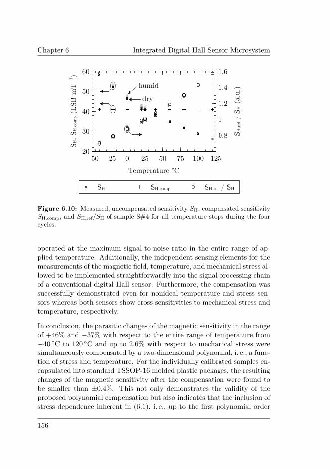
The changes of the magnetic sensitivity ∆SH (2.7) is found similarly, i. e.,
∆SH (Ti) = SH,humid (Ti)− SH,dry (Ti) (3.8)
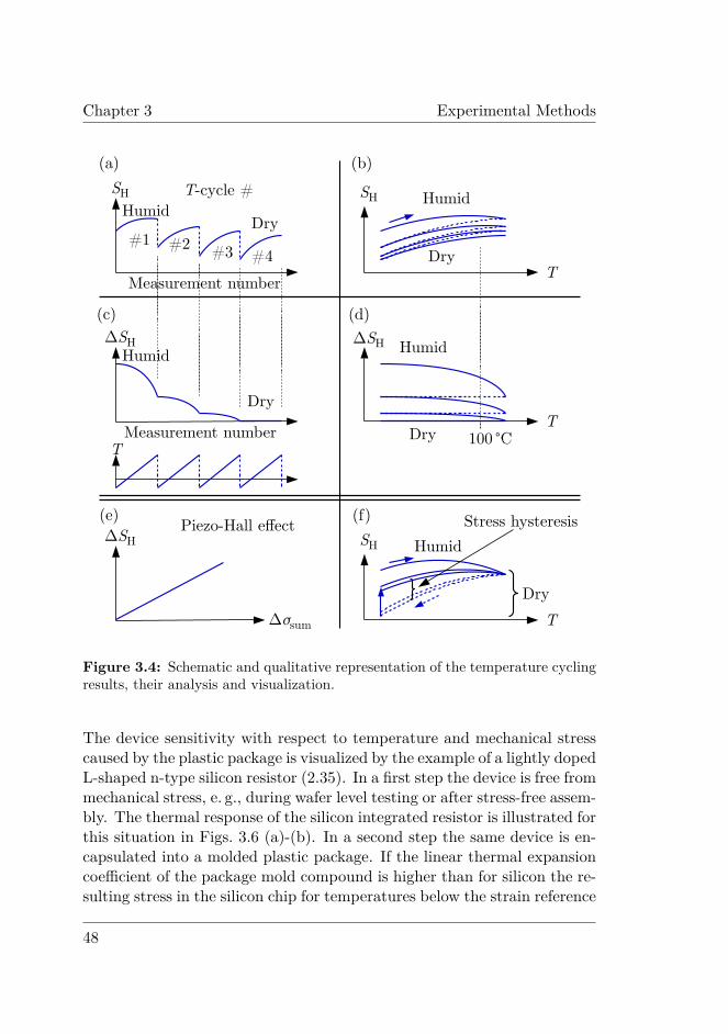
Thereby the obtained measurements can be visualized as either absolutevalues or as the change between the cycles both with respect to the tem-perature or the measurement number, as shown in Figs. 3.4 (a)-(d). More
46
3.3 Stress-Free Assembly
importantly, the described measurement and analysis method enables fourkey features to be extracted:
1. The thermal behavior of the Hall sensor for different package humid-ity levels, as shown in Fig. 3.4 (b).
2. The sensitivity change ∆SH between the humid and dry packagestates without and with the parasitic impact of the temperature, asshown in Figs. 3.4 (c) and (d), respectively.
3. The correlation between parameters, e. g., ∆SH and ∆σsum, as shownin Fig. 3.4 (e).
4. The difference between the two parts of the temperature cycle withrising and falling temperature, i. e., stress hysteresis, as shown inFig. 3.4 (f).
3.3 Stress-Free Assembly
The purely thermal behavior of the resistors, Hall elements, and stresssensors cannot be characterized with packaged devices due to the para-sitic impact of mechanical stress with changing temperature. Therefore astress-free assembly of silicon integrated circuits onto ceramic Al2O3 sub-strates was used for the samples fabricated with 0.35µm CMOS technology.The samples fabricated with 0.18µm CMOS technology were assembled onFR4 PCB substrates. The two assembly types are called chip-on-ceramic(COC) and chip-on-board (COB) assembly, respectively. The silicon chipis attached to the substrate with soft glue whereby Ablebond 84-3 MV fromAblestik was chosen. The electrical connection is achieved with Au bondwires between the chip and the PCB, which is plated with a 0.1-µm-thickgold layer to allow reliable wire bonds. By finally covering the chip andthe bond wires with a soft, nontransparent silicone glob top it is ensuredthat the circuits are shielded from ambient light and that the magnitudeof mechanical stress is negligible compared to packaged devices in stan-dard molded plastic packages. As soft glob top material Eccobond S7503from Henkel was selected. The schematic cross-section of the stress-freeassembly, along with photographs of COB and COC samples, are shownin Figs. 3.5 (a), (b), and (c), respectively.
47
Chapter 3 Experimental Methods
Measurement number
Measurement number
(a) (b)
(c) (d)
SH SH
T
T
∆SH
Humid
Dry
∆SH
T-cycle #
#1 #2 #3 #4
100 °CT
SH
T
Humid
Dry
(e) (f)∆SH
∆σsum
Piezo-Hall effect
Humid
Dry
HumidDry
Stress hysteresis
Humid
Dry
Figure 3.4: Schematic and qualitative representation of the temperature cyclingresults, their analysis and visualization.
The device sensitivity with respect to temperature and mechanical stresscaused by the plastic package is visualized by the example of a lightly dopedL-shaped n-type silicon resistor (2.35). In a first step the device is free frommechanical stress, e. g., during wafer level testing or after stress-free assem-bly. The thermal response of the silicon integrated resistor is illustrated forthis situation in Figs. 3.6 (a)-(b). In a second step the same device is en-capsulated into a molded plastic package. If the linear thermal expansioncoefficient of the package mold compound is higher than for silicon the re-sulting stress in the silicon chip for temperatures below the strain reference
48
3.4 Silicon Integrated Circuits and Assemblies
48 bond pads
48 pins
Device under test
Siliconesoft glob top
16 bond pads
16 pins
Device under test
Siliconesoft glob top
(b) Chip-on-board (COB) (c) Chip-on-ceramic (COC)
(a) Cross section Silicone soft glob top
Bond wires
Silicon chip
Soft glue
Substrate
Ceramic substrate
PCB substrate
Figure 3.5: Stress-free assembly of the silicon integrated circuits. (a) cross-section; (b) chip-on-board assembly using a printed circuit board (PCB) substrate;(c) chip-on-ceramic assembly using an Al2O3 substrate.
temperature is compressive. The strain reference temperature is identicalto the molding temperature Tmold. The sum of in-plane normal stressesin compressive direction combines with the negative piezoresistance coef-ficient of the n-type L-shaped resistor, i. e., (π11 + π12)/2 = −0.24 GPa−1
obtained with the values from Table 2.3. Therefore the resistance of thepackaged silicon is higher than for the stress-free device for T < Tmold, asillustrated in Figs. 3.6 (c)-(d).
3.4 Silicon Integrated Circuits and Assemblies
A number of silicon integrated circuits has been developed and realized inthe course of this work. Standard 0.35µm and 0.18µm CMOS technologiesfrom X-Fab Silicon Foundries were used for their fabrication. On the one
49
Chapter 3 Experimental Methods
Stress-free assembly(a) (b)
(c) (d)
σxx+σyy RL
T
T
RL
T
σxx+σyy
T
Tmold
Molded plastic package
Tmold
RL(T)
RL(T)
RL(T,σ)
Figure 3.6: Illustration of the package mechanical stress with respect to tem-perature and the corresponding response of a n-type silicon resistor with respectto temperature and mechanical stress. Linear thermal expansion coefficients areassumed for the molded plastic package.
hand, device and circuit experiments have been implemented for the proofof principle of the sensing elements and methods. On the other handfully integrated Hall sensor microsystems with analog and digital signalprocessing chains have been realized with teams of engineers at Melexis inorder to test these sensing elements and methods in a product environment.
The device and circuit test chips contain various resistor types in fourorientations, i. e., 0, 45, 90, and 135 with respect to the wafer flat,alongside with conventional and metal-oxide-semiconductor (MOS) Hallplates as well as stress sensors. These devices were implemented in bothtest chip versions, i. e., 0.35µm and 0.18µm CMOS technologies. Addi-tionally the 0.18µm test chips include temperature sensors, and a bandgapreference. The layouts of the device test chips are shown in Figs. 3.7 (a)-(d). The layouts of the Hall sensor microsystems with analog and digitalsignal processing chains are shown in Figs. 3.8 (a) and (b), respectively.
The silicon integrated circuits are assembled according to the requirementsof the three setups presented in Sections 3.1 to 3.3. Silicon strips are
50
3.4 Silicon Integrated Circuits and Assemblies
(a) (b)
(c) (d)
Bond padsMOS Hall plates
In-plane resistors
Hall plates withstress sensors
Bandgap 1.2 V
PTAT
Temperaturesensor
Hall plates withstress sensors
Supply ring, 24 bond pads Supply ring, 16 bond pads
Totally 87experiment
cells
Figure 3.7: Layouts of silicon integrated circuits containing experimental devicesfabricated in 0.35µm (a)-(b) and 0.18µm (c)-(d) CMOS technologies.
needed for the bending bridge. Chip-on-board and chip-on-ceramic assem-bly is used for the stress-free but temperature-dependent measurements.The temperature cycling has been conducted on samples encapsulated intostandard molded plastic packages, i. e., SOIC-8, single-in-line, dual mold,TSSOP-16, and TSSOP-24 packages. The different assemblies are shownin Fig. 3.9.
51
Chapter 3 Experimental Methods
Hall plates withstress sensors
(a) (b)
Hall plates withstress sensors
Temperature sensor
Figure 3.8: Layouts of silicon circuits containing fully integrated Hall sensormicrosystems. (a) Hall sensor with an analog signal processing chain; (b) Hallsensor with a digital signal processing chain.
(b) Chip-on-boardChip-on-ceramic
(c) Molded plasticpackages
(a) Si-strip
SOIC-8
Dual mold
120
6
10045 80
35 14
56
Au wire bonds
DUT
TSSOP-16
Single-in-line(SIP)
Figure 3.9: Overview of the different assemblies used throughout this work.All dimensions are in (mm). (a) silicon strip assembly for the four-point bend-ing bridge, (b) stress-free chip-on-board and chip-on-ceramic assemblies, and (c)molded standard plastic packages. The TSSOP-24 package is omitted from thefigure.
52
3.5 Data Acquisition System and Instrumentation
3.5 Data Acquisition System and Instrumenta-tion
The silicon-integrated devices under test (DUT) are electrically character-ized with respect to temperature, magnetic field, mechanical stress, andvarious electrical supply conditions. The operation of the Hall plates inseveral supply and measurement configurations, i. e., Hall, van der Pauw,and spinning current necessitates the use of a switch matrix. The demandfor a high degree of automation as well as the need for flexible connectivityof the DUT with respect to two-wire and four-wire connections led to thedesign of a custom-made switch matrix.
Switch Matrix Design The switch matrix is remotely controlled viathe universal serial bus (USB). The settings are stored in an on-boardcontrol logic and transmitted to the total of 256 relay switches availableon four stacked PCBs. A single board contains 64 relay switches andrelates 16 × 4 single-ended analog channels. Up to four boards can bestacked resulting in a variety of matrix configurations, i. e., 64× 4, 32× 8,or 16 × 16 channels. A schematic diagram of the switch matrix togetherwith the possible configurations of the four individual boards are shown inFig. 3.10. The relay switches are chosen for their low serial resistance ofbelow 0.2 Ω and their low current consumption below 3.5mA. The switchmatrix is supplied via the 5 V supply available from the USB. A photographof a single switch matrix board is shown in Fig. 3.11.
Instrumentation In order to ensure at the same time a high stabilityand accuracy of the source and measurement units (SMU) while keep-ing a high level of flexibility, the electrical characterization of the siliconintegrated devices and circuits is performed with a HP4156C PrecisionSemiconductor Parameter Analyzer. The temperature of the DUT is con-trolled with a Votsch VCL7006 climate chamber or alternatively with aconstant flow of dry air obtained from a FTS thermostream. A currentsource drives a constant current through the Helmholtz coil in order togenerate a controlled magnetic field. Current sources from KEPCO andHAMEG were used.
53
Chapter 3 Experimental Methods
USBconnector Control logic
256 relay switches
16 to 64 single-ended analog channels
4 to 16single-endedanalog
channels
256
Board configurations64 × 4
32 × 816 × 16
Singleboard
16
4
5 V supply
Figure 3.10: Schematic diagram of the switch matrix with a total of 256 in-dividual relay switches on four stacked boards, each with 64 switches. A singleboard is designed with 4 instrument channels and 16 DUT channels. The fourboards can be stacked to offer 64× 4, 32× 8, or 16× 16 channels, as shown in theinset.
Data Acquisition System The instruments are connected to the Linuxcomputer via the general purpose instrument bus (GPIB), ethernet, or theUSB. They are configured and controlled remotely via a Python scriptrunning on the computer. A schematic diagram of the data acquisitionsystem is shown in Fig. 3.12. The switch matrix is assembled with 16× 8channels in order to connect the 16 pins of the integrated circuit with the8 instruments of the HP4156C parameter analyzer. A photograph of thedata acquisition system is shown in Fig. 3.13.
54
3.5 Data Acquisition System and Instrumentation
Data bus,address bus,control bus
16×4 relay switches
16 analog channels
4 analogchannels
Figure 3.11: Photograph of the custom-made switch matrix. A single boardwith 64 individual relay switches is shown. The board is designed with 16 × 4single-ended analog channels.
Linuxcomputer&Python
Current sourceGPIB
Climate chamber
Ethernet
Helmholtz coil
DUT16
Switchmatrix
HP4156C8
USB
GPIB
Figure 3.12: Schematic diagram of the data acquisition system. The switchmatrix is assembled with two boards in order to connect the eight instrumentchannels of the HP4156C parameter analyzer with the 16 pins of the DUT.
55
Chapter 3 Experimental Methods
Linux PC withPython console
HP4156C SemiconductorParameter Analyzer
Custom-made 16×8 channel switch matrix
Current source
Climate chamber
Figure 3.13: Photograph of the entire data acquisition system.
56
Chapter 4
Stress and Temperature Sensing
The goal to actively compensate the stress-related sensitivity change ofplanar Hall sensors necessitates CMOS-compatible integrated devices tomeasure the desired components of the mechanical stress and the temper-ature. Both topics are addressed throughout this chapter, including
1. a package stress sensor in Section 4.1,
2. a temperature sensor in Section 4.2,
3. a combined stress and temperature sensor in Section 4.3, and
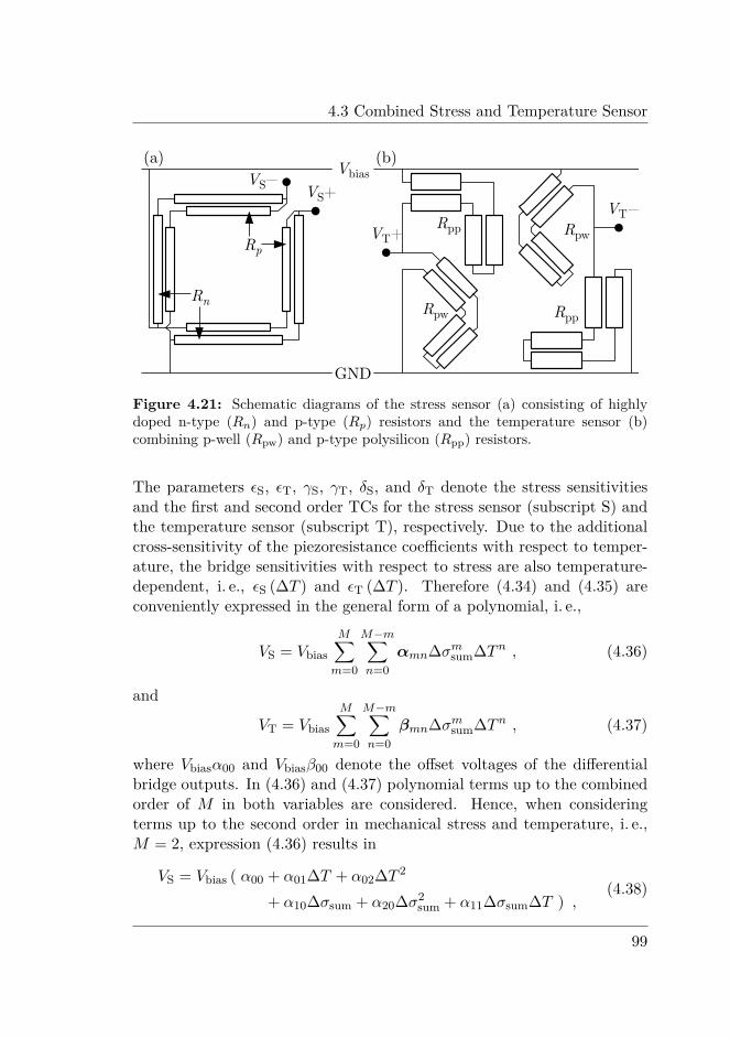
4. a combined Hall and stress sensor in Section 4.4.
4.1 Package Stress Sensor
4.1.1 Introduction
The magnetic sensitivity of CMOS planar Hall elements is compromisednot only by temperature for the compensation of which integrated tem-The stress sensor has been published at the IEEE Sensors Conference 2012 [72] and in theIEEE Sensors Journal [73]. The author contributed the idea, design and implementationof test structures, and the experimental validation. Additionally the stress sensor hasbeen patented under EP2490036 [74].
57
Chapter 4 Stress and Temperature Sensing
perature sensors are the state-of-the-art solution, but also by mechanicalstress. Via the piezo-Hall effect, as introduced in Section 2.5 the in-planeand out-of-plane normal stress components are known to cause a change ofthe current-related magnetic sensitivity. For the compensation of this un-desired cross-sensitivity we intend to use an integrated stress sensor whichmeasures the relevant mechanical stress. Therefore, in view of (2.40), thestress sensor is required to respond isotropically to the in-plane normalstresses. Overall the desired properties of the stress sensor may be de-scribed as follows. The sensor has to:
• be compatible with standard CMOS technology,
• offer a differential output voltage,
• provide isotropic sensitivity with respect to the in-plane normal stresses,and
• show only a minimal thermal cross-sensitivity.
CMOS Stress Sensors CMOS-compatible stress sensors [75] have beenrealized utilizing the piezo-junction [76], piezo-Hall [58], pseudo-Hall [71]and by far most often the piezoresistance [53, 59, 62, 77–79] effects. Someof these devices are even capable of sensing multiple independent stresscomponents simultaneously [38, 60]. Moreover, upon vertical current flowthe measurement of the out-of-plane normal [80] and shear stresses [81]has been enabled. Applications of piezoresistive stress sensors include diestress mapping [82], in-situ deformation analysis [61], structural analysisof electronic packages [46], assembly and bonding process monitoring [83],medical devices [84], and many more.
For most applications the sizeable piezoresistive coefficients are an essentialfeature as, e. g., in CMOS pressure sensors [44]. Additionally, the piezore-sistance effect in CMOS silicon is anisotropic. Therefore the response ofthe piezoresistors depends on the orientations of the current flow, the me-chanical stress, and the silicon crystal. On the other hand, piezoresistorssuffer from a relatively high parasitic cross-sensitivity to temperature, asprominently present in conventional sensor rosettes [85].
In view of the designated usage of the sensor both the anisotropy andthe thermal cross-sensitivity are parasitic effects. The task is therefore to
58
4.1 Package Stress Sensor
Rn
Hall plate
Rn
Rp
Rp
Vbias
VS
+
–
(a) (b)Vbias
GND
RL,n
RL,nRL,p
RL,p
GND
VS+ VS−
Figure 4.1: Schematic diagram of the stress sensor. Eight highly doped n-typeand p-type piezoresistor segments Rn and Rp, respectively, are placed aroundthe Hall plate (a). The piezoresistor segments are connected to form orthogonalpairs resulting in four L-shaped resistors RL,n and RL,p, respectively, building theWheatstone bridge (b). Adapted from [73].
overcome these limitations and to design a bridge-type piezoresistive stresssensor providing at the same time an isotropic sensitivity with respect tothe in-plane normal stresses and a small thermal cross-sensitivity.
4.1.2 Design
The stress sensor consists of eight appropriately arranged resistor segmentsmade of highly doped n-type (Rn) and p-type (Rp) material. These resistorsegments are connected into orthogonal pairs resulting in four L-shapedresistors with resistance values RL,n and RL,p. A schematic diagram ofthe resistor arrangement is given in Fig. 4.1 (a). The pairwise orthog-onal connection ensures that the desired stress-related resistance changeis achieved: the response is isotropic with respect to the normal in-planestress components. The four L-shaped resistors form a Wheatstone bridge,as shown in Fig. 4.1 (b). Thereby the combination of n-type and p-typeresistors is responsible for the desired stress-related response.
59
Chapter 4 Stress and Temperature Sensing
The combination of n-type and p-type resistors in the same Wheatstonebridge has some drawbacks related to the expected resistor mismatch.These parasitic effects are discussed in Subsection 4.1.3 whereas at thesame time solutions are presented to overcome these issues. On the otherhand the implementation of the bridge using highly doped resistors bringsseveral advantages which are summarized in Subsection 4.1.6.
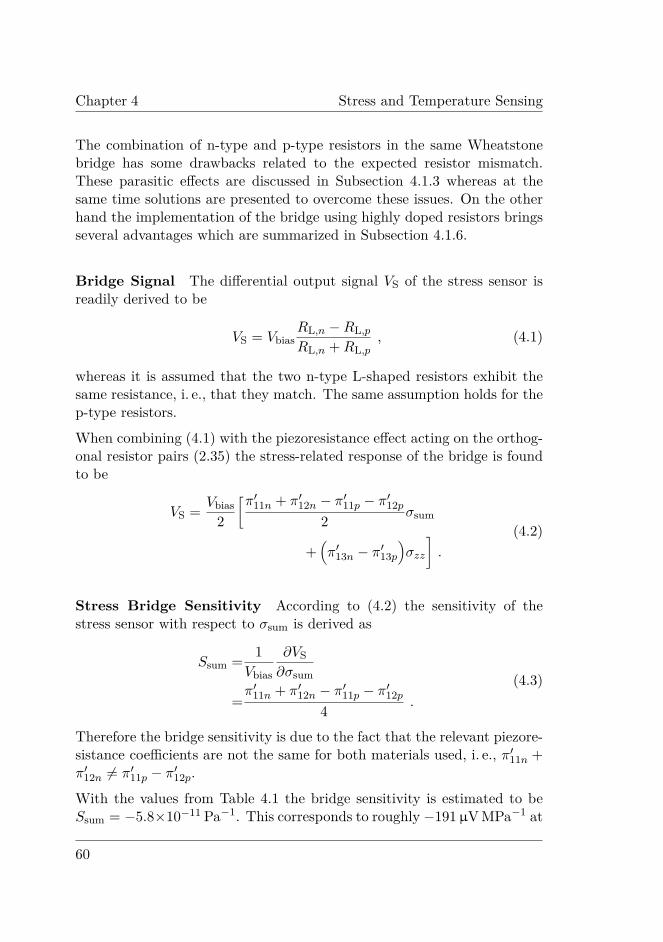
Bridge Signal The differential output signal VS of the stress sensor isreadily derived to be
VS = VbiasRL,n −RL,pRL,n +RL,p
, (4.1)
whereas it is assumed that the two n-type L-shaped resistors exhibit thesame resistance, i. e., that they match. The same assumption holds for thep-type resistors.
When combining (4.1) with the piezoresistance effect acting on the orthog-onal resistor pairs (2.35) the stress-related response of the bridge is foundto be
VS = Vbias2
[π′11n + π′12n − π′11p − π′12p
2 σsum
+(π′13n − π′13p
)σzz
].
(4.2)
Stress Bridge Sensitivity According to (4.2) the sensitivity of thestress sensor with respect to σsum is derived as
Ssum = 1Vbias
∂VS∂σsum
=π′11n + π′12n − π′11p − π′12p
4 .(4.3)
Therefore the bridge sensitivity is due to the fact that the relevant piezore-sistance coefficients are not the same for both materials used, i. e., π′11n +π′12n 6= π′11p − π′12p.
With the values from Table 4.1 the bridge sensitivity is estimated to beSsum = −5.8×10⁻¹¹ Pa−1. This corresponds to roughly −191µV MPa−1 at
60
4.1 Package Stress Sensor
Table 4.1: Approximate piezoresistive coefficients for the highly doped n-typeand p-type resistors in (100)-silicon. The values are given for resistors orientedalong the 〈100〉 and 〈110〉 crystal directions at a doping level of 7 × 1019 cm−3
Vbias = 3.3 V. Hence, as an example, for σsum = −100 MPa, cf. Section 2.6,the differential output signal is expected to be VS ≈ 19 mV.
On the other hand, as evident from (4.2) the stress sensor is sensitive notonly to σsum but also to the out-of-plane normal stress, i. e., σzz. Thecorresponding sensitivity is found to be
Szz = 1Vbias
∂Vbridge∂σzz
=π′13n − π′13p
2 . (4.4)
Using the values from Table 4.1 the out-of-plane bridge sensitivity is esti-mated to be Szz ≈ 0.11GPa−1 . For a typical out-of-plane normal stressof 5MPa, cf. Section 2.6, and a supply voltage of Vbias = 3.3V an outputsignal of VS ≈ 1.8mV can be expected. This value is ten times smallerthan the value previously obtained for in-plane normal stress in the samepackage. Therefore in the forthcoming description and expressions theout-of-plane contribution is mostly omitted. Note however that all themethods are valid for in-plane as well as out-of-plane stresses, as discussedin Subsection 4.1.4.
61
Chapter 4 Stress and Temperature Sensing
4.1.3 Parasitic Effects and their Elimination
Rn − Rp Mismatch A major concern of the proposed sensor is themismatch between the n-type and the p-type resistors. Such a mismatchµ may be expressed by
RL,n = RL,0 (1 + µ) (4.5)
andRL,p = RL,0 (1− µ) , (4.6)
where RL,0 denotes the average value of the n-type and p-type resistances.
When combining (4.1) with (4.5) and (4.6) the mismatch is found to causean offset voltage in the bridge output. Hence VS (4.1) consists of a stress-dependent Vσ and a stress-independent Voff contribution, i. e.,
VS = Vσ + Voff . (4.7)
The value of the offset voltage is found to be
Voff = µVbias . (4.8)
The offset voltage can be subtracted from the bridge output in order toobtain the purely stress-related signal, i. e., Vσ = VS − Voff. Ideally Voff isobtained in the absence of mechanical stress, e. g., during wafer probingwhen σsum ≈ 0 MPa.
On the other hand the RL,n − RL,p mismatch may have a noticeable im-pact on Ssum. The Taylor series expansion of (4.1) with respect to σsum,combined with (4.5), (4.6), and (2.35) yields
VSVbias
= µ+(1− µ2
) π′11n + π′12n − π′11p − π′12p4 σsum +O
(σ2sum
), (4.9)
where O(σ2sum)denote second and higher order terms in σsum. Hence, Ssum
(4.3) is decreased by 1% for a mismatch of µ = 0.1 which is expected forthe process corners. This effect is removed by the appropriate selection ofthe parameter λ introduced in Subsection 4.1.4.
62
4.1 Package Stress Sensor
R⊥−R‖ Mismatch The matching of the orthogonal resistor segmentsforming the L-shaped resistors is assumed in expressions (2.35) and (4.2).In a real stress sensor, however, the matching can not be guaranteed. Amismatch between the orthogonal resistor segments may occur due to, e. g.,mask misalignment, a temperature gradient, or the junction field effect.As evident from Fig. 4.1 the orthogonal segments are naturally exposedto different potentials which in combination with the junction field effectleads to a systematic resistor mismatch. In analogy to (2.36) and (2.37)such a mismatch ν is defined via
Rp,‖ = R0 (1 + ν) (4.10)
andRp,⊥ = R0 (1− ν) , (4.11)
for the p-type resistors with orientations parallel and perpendicular to thewafer flat, respectively.
For their series connection one finds
Rp‖ +Rp⊥ = 2R0
[1+
π′11p + π′12p2 σsum
+π′13pσzz
+νπ′11p − π′12p
2 σD
].
(4.12)
The expression is similar to (2.38) with the difference, however, that herethe term with respect to the in-plane shear stress vanishes due to thepresent restriction of the resistor orientations to 〈110〉 directions. Thereforethe mismatch ν leads to a parasitic sensitivity to σD. The impact can beavoided by minimizing the mismatch ν, the difference of the piezoresistancecoefficients, i. e., π′11p−π′12p, or σD. Analogous expressions are found for then-type resistors. By using the highly doped n-type and p-type resistors, asopposed to lightly doped well resistors, the part of the mismatch originatingfrom the junction field effect is strongly reduced.
Temperature Coefficient Mismatch Finally, a mismatch between thetemperature coefficients of the n-type and the p-type resistances leads toa temperature-dependent offset voltage, i. e., Voff(T ). With reference to
63
Chapter 4 Stress and Temperature Sensing
(2.32), the temperature dependence of the n-type L-shaped resistors canbe expressed as
RL,n = RL,0(1 + αn∆T + βn∆T 2
), (4.13)
and similarly for the p-type resistors. With (4.1) including the mismatch(4.5) and (4.6) the Taylor series expansion of the temperature-dependentoffset voltage is found to be
VoffVbias
= µ+(1− µ2
) αn − αp2 ∆T +O
(∆T 2
). (4.14)
Evidently, Voff(T ) is a function of the difference between the temperaturecoefficients of resistance of the n-type and the p-type resistors, i. e., αn −αp. To provide a low thermal cross-sensitivity the matching between thetemperature coefficients is crucial. This is achieved, again, by using highlydoped n-type and p-type resistors.
4.1.4 Compensation of the Piezo-Hall Effect
The purpose of the stress sensor is the compensation of the piezo-Halleffect affecting the magnetic sensitivity of the planar Hall plate, i. e., SH =SH,0 (1 + P12σsum) cf. (2.40). This compensation is achieved by using aportion of Vσ to counterbalance the relative sensitivity change, i. e.,
SH,comp = SH1
1− λVσ≡ SH,0 , (4.15)
where SH,comp is the compensated sensitivity and λ denotes the compen-sation gain which ensures that the compensated sensitivity remains equalto its stress-free value, i. e., SH,comp = SH,0.
The task therefore is to determine λ. By combining (4.15) with (2.40),(4.2), and (4.3) one finds
SH,comp = SH,01 + P12σsum
1− λSsumσsumVbias. (4.16)
Replacing Ssum by the right hand side of (4.3) reveals
λ = − 4P12
Vbias(π′11,n + π′12,n − π′11,p − π′12,p
) . (4.17)
64
4.1 Package Stress Sensor
With the values from Tables 2.5 and 4.1 the compensation gain is expectedto be λ = 2.2 V−1 at Vbias = 3.3 V.In view of the envisaged integration of the piezo-Hall effect compensationinto Hall sensor microsystems, the first-order approximation of (4.15) is ofparticular interest, i. e.,
SH,comp = SH (1 + λVσ) . (4.18)
In (4.18) the compensation is based on a multiplication rather than adivision, cf. (4.15). Moreover it will be shown in Chapter 5 that this formcan be implemented in purely analog circuitry.Note that higher-order terms in σsum have been neglected in (2.40) aswell as in (2.35) and consequently in (4.2). Therefore (4.18) indeed ap-proximates (4.15) correctly up to the first order in mechanical stress,i. e., σsum. Additionally, the compensation in its first-order approxima-tion (4.18) works with less than 1% deviation from its ideal form (4.15)for values of |λVσ| ≤ 0.1, i. e., 10% of stress-related sensitivity change ex-pected for a change of mechanical stress of ∆σsum = 250 MPa. Therefore,in view of the expected package stress, cf. Section 2.6, the first-order ap-proximation is largely acceptable for most integrated Hall sensor systemsencapsulated into standard molded plastic packages.
In-plane versus Out-of-Plane Mechanical Stress Expressions (4.16)and (4.17) are derived neglecting the impact of the out-of-plane mechan-ical stress present in (2.40) and (4.2). However, it may be noted withthe values from Table 4.1 that the ratio between the sensitivities of thestress sensor with respect to in-plane and out-of-plane normal stress yieldsSsum/Szz ≈ −0.50. Similarly, for the piezo-Hall effect the ratio is found tobe P12/P11 ≈ −0.49 using the values of the piezo-Hall coefficients from Ta-ble 2.5. Therefore the compensation according to (4.15) as well as (4.18) isvalid when the device is exposed to both in-plane and out-of-plane stresses.The corresponding error in the compensation gain is expected to be assmall as 2%. In other words, when exposing the device to out-of-planenormal stress the compensation gain is found to be
λzz = − 2P11Vbias(π′13,n − π′13,p)
, (4.19)
which except for a difference of about 2% corresponds to (4.17).
65
Chapter 4 Stress and Temperature Sensing
4.1.5 Process and Temperature Related Variations of λ
The compensation gain λ originates from the ratio between the piezo-Halland the piezoresistance coefficients, as derived in (4.17). Due to varia-tions of the doping density and profile the piezo-Hall and piezoresistancecoefficients, and consequently λ may experience variations. In a first stepa rough estimation of λ indicates its boundaries for different CMOS pro-cesses whereby precise values of the doping densities are unknown andmust be calculated on the basis of sheet resistance and junction depth. Onthe other hand, in a second step, the variation of λ is calculated for thelot-to-lot variations of the doping densities of about ±10%.
Rough Estimation of λ For a strongly and a lightly doped n-well,P12 is estimated to take values of 3 × 10⁻¹⁰ Pa−1 and 4.5 × 10⁻¹⁰ Pa−1,respectively [14]. For the highly doped piezoresistors the piezoresistancecoefficients are expected to lie within 25% to 50% of the values measuredfor lightly doped material [43,47]. These variations result in compensationgain values ranging from λmin = 1.5 V−1 to λmax = 4.5 V−1. This strongvariation is dominantly due to the doping dependence of the piezoresistancecoefficients [43,47,48].
Lot-to-Lot Variation of λ When fabricating devices in the same tech-nology, lot-to-lot variations of the doping density of approximately ±10%can be expected. Under this assumption the value of P12 is estimatedto lie within 3.98 × 10⁻¹⁰ Pa−1 and 4.03 × 10⁻¹⁰ Pa−1 [14]. Similarly, thepiezoresistance coefficients of the highly doped bridge resistors are expectedto reach levels between 40.4% and 42.4% of the values obtained for lightlydoped silicon [43, 47, 48]. Consequently, λ takes values between 2.15 V−1
and 2.28 V−1 for a supply voltage of 3.3 V and therefore deviates by only±3% from its target value of 2.2 V−1.
Temperature Dependence of λ The piezo-Hall and piezoresistancecoefficients are functions of the temperature, hence a temperature depen-dence must be expected for the compensation gain as well, i. e., λ(T ).Following (2.41) the first-order TC of the piezo-Hall coefficient of lightlydoped n-type silicon was found to be −1.7 × 10⁻³ K−1 [14]. Similarly,
66
4.1 Package Stress Sensor
in view of (2.31), for the strongly doped piezoresistors a first-oder TC of−1.0 × 10⁻³ K−1 is expected [43, 47, 48]. Therefore the resulting λ is ex-pected to experience less than ±10% variation for a temperature changeof ±100 K.
4.1.6 Implementation
The stress sensor was implemented in a standard 0.35µm CMOS tech-nology fabricated at X-Fab Silicon Foundries. The highly doped n-typeand p-type materials were used to form long and narrow resistor segmentsarranged at orientations parallel and perpendicular to the wafer flat, i. e.,along the 〈110〉 crystal directions. In this way the resistor segments are ar-ranged around the Hall plate and, in fact, surround it entirely. The layoutimplementation of the stress sensor is shown in Fig. 4.2. The dimensionsof the piezoresistor segments are summarized in Table 4.2 along with theirnominal Rnom and observed resistances Rmeas at room temperature.
The stress sensor has a size of 60µm× 60µm, leaving in its center a spaceof 46µm × 46µm for the Hall element. The nominal resistance of thebridge is 10 kΩ. At Vbias = 3.3 V a supply current of 0.33 mA and a powerconsumption of roughly 1 mW are expected.
High versus Low Doping The use of the highly doped rather thanlightly doped resistors comes at the cost of a lower stress-related sensitiv-ity. When estimating Ssum (4.3) with the piezoresistance coefficients ofTable 4.1 rather than those of Table 2.2 it is found that the sensitivityusing highly doped resistors decreases to about 50% of the value obtainedfor lightly doped resistors.
On the other hand, the use of highly doped resistors brings several advan-tages.
1. In order to obtain reasonable resistance values the highly doped re-sistors are implemented as long and narrow structures due to the lowsheet resistance. These structures are easily placed around the Hallplates.
2. Highly doped resistors have smaller temperature coefficients of resis-tance. Moreover they were found to match surprisingly well between
67
Chapter 4 Stress and Temperature Sensing
Table 4.2: Dimensions and sheet resistance values of the highly doped n-typeand p-type piezoresistor segments, their nominal and measured resistances Rnomand Rmeas, respectively. The values of Rmeas were obtained from a stress-freeCOB sample. Adapted from [73].
Resistor type L W R Rnom Rmeas
(µm) (µm) (Ω) (kΩ) (kΩ)
n 42 0.7 85 4.98 4.62p 48.3 1 90 4.96 5.25
the n-type and the p-type materials which results in a small thermalcross-sensitivity of the bridge output signal VS.
3. The junction field effect is smaller in highly doped resistors, leadingto a smaller mismatch among the orthogonal segments forming theL-shaped resistors. Therefore the parasitic cross-sensitivity to σD(4.12) can be minimized.
4. The highly doped resistors are available as standard devices in theCMOS technology featuring appropriate process control and moni-toring (PCM). In contrast, isolated p-well resistors need to be em-bedded inside an additional deep n-well. Therefore p-well resistorsmay not be straightforwardly available.
In conclusion, these advantages led to the deliberate choice of using highlydoped resistors. The loss of sensitivity is counterbalanced by the appro-priate selection of λ.
4.1.7 Experimental Results
Characterization Setup and Method The sensitivity of the stresssensor with respect to in-plane normal stress and its temperature-relatedparasitic cross-sensitivity were experimentally verified. Thereafter the ef-fectivity of the proposed compensation method was validated with devicesin standard molded plastic packages. Therefore samples were exposed to
68
4.1 Package Stress Sensor
Hall platearea
Rn
N-well contact
Rp
60 μm
46 μm
Figure 4.2: Layout of the stress sensor in a standard 0.35µm CMOS technologyfabricated at X-Fab Silicon Foundries. Highly doped n-type and p-type piezore-sistors are used to form a Wheatstone bridge. The resulting long and narrowresistor segments are arranged to surround the Hall plate for which a space of46µm× 46µm is available. Adapted from [73].
in-plane normal stress at room temperature by using the four-point bend-ing bridge, as described in Section 3.1. Additionally, samples were assem-bled by the stress-free COB assembly, as described in Section 3.3. Thesesamples were exposed to temperature change with negligible impact fromthe mechanical stress. Finally, samples were encapsulated into single-in-line and dual mold packages. Their magnetic sensitivities and stress sensorresponses were measured during humid-to-dry cycling as described in Sec-tion 3.2. Temperatures between −40 C and 125 C were applied duringfour successive cycles.
Four-Point Bending Bridge The sample #1 was obtained by cutting a100-mm-long and 6.7-mm-wide strip from a 380-µm-thick wafer. The DUTis located in the center of the strip and exposed to in-plane normal stressesσxx from 0 MPa to 40 MPa at room temperature. Simultaneously, for eachstress value the sample was exposed to out-of-plane magnetic fields between
69
Chapter 4 Stress and Temperature Sensing
0 mT and 15 mT measuring the output voltage of the stress sensor and themagnetic sensitivity of a planar Hall plate. The measurement results ofsample #1 are shown in Fig. 4.3.
The differential output voltage of the stress sensor VS at room temperatureand σxx = 0 MPa, i. e., the offset voltage was found to be Voff = 190.5 mVat Vbias = 3.3 V. The offset is caused by the mismatch between the n-type and p-type resistors which is found to be µ = 0.058. With increasingtensile stress σxx, VS was observed to decrease linearly. The correspondingsensitivity (4.3) was extracted to be Ssum = −4.7×10⁻¹¹ Pa−1. This valueis slightly smaller than expectated, which is likely caused by the differencesin the doping profile and density.
The magnetic sensitivity was found to change linearly with the appliedmechanical stress. The slope corresponds to the piezo-Hall coefficient forin-plane stress. Its value was extracted to be P12 = 0.41×10⁻⁹ Pa−1 whichis close to the expectation. In summary, both changes are proportional toeach other, indicating that VS may be used for the intended compensa-tion of the piezo-Hall effect. To fulfill this task the compensation gainintroduced in (4.15) must be used. Its value can be extracted from theabove measurements, i. e., λ = −P12/(SsumVbias) and is readily found tobe λ = 2.6 V−1. This value is slightly higher than the estimated one. Thediscrepancy is caused by the somewhat smaller Ssum.
Thermal Response Sample #2 assembled by stress-free COB assemblywas exposed to temperatures between −37 C and 100 C. Due to theabsence of mechanical stress these measurements represent the offset of thestress sensor as a function of temperature, i. e., Voff(T ). The correspondingmeasurements are shown in Fig. 4.4. For this sample an offset voltage at25 C of Voff = 211.7 mV was found. For the applied temperatures theoffset was observed to vary between 190 mV and 220 mV. Therefore thetemperature-related change of the offset voltage was found to be as smallas ∆Voff = 30 mV for Vbias = 3.3 V. A second-order model, i. e., Voff/Vbias =µ+γ∆T+δ∆T 2 cf. (4.14) was fit to the measurements. The correspondingparameters were extracted to be µ = 0.064, γ = 0.074 × 10⁻³ K−1, andδ = −0.55× 10⁻⁶ K−2.
On the other hand the thermal response of the stress sensor was mea-sured for sample #3 packaged into a standard single-in-line package. This
70
4.1 Package Stress Sensor
Figure 4.3: Differential output voltage VS of the stress sensor and the relativevalue of the magnetic sensitivity of a planar Hall plate as a function of mechanicalstress at room temperature. The measurements of sample #1 at a supply voltageof Vbias = 3.3 V are shown. Adapted from [73].
Figure 4.4: Stress sensor output as a function of temperature for sample #2assembled by stress-free COB assembly. The measurements represent Voff(T )in the absence of mechanical stress. A second-order model, i. e., Voff/Vbias =µ+ γ∆T + δ∆T 2 was fit to the measurements (solid line). Adapted from [73].
71
Chapter 4 Stress and Temperature Sensing
Figure 4.5: Stress sensor output as a function of temperature during four succes-sive measurement cycles of sample #3 packaged in a single-in-line package. Solidlines are guides to the eye visualizing the humidity-related stress change and thestress hysteresis. Adapted from [73].
sample underwent the humid-to-dry cycling process with four temperaturecycles between −40 C and 125 C. The measurements of VS are shownin Fig. 4.5 for the four temperature cycles. A change of the stress sensoroutput of ∆Vσ = 3 mV was observed between the first humid cycle and thesubsequent dry cycles. This corresponds to a change of the in-plane nor-mal stresses of approximately ∆σsum = −20 MPa utilizing the previouslyextracted Ssum.
Additionally, when comparing rising and falling temperature cycles a hys-teresis of up to 3 mV could be observed with the stress sensor at 25 C.Therefore when the room temperature was approached from 125 C thepackage exerted roughly −20 MPa more (compressive) stress on the siliconchip than when room temperature was approached from −40 C. This hys-teresis was likely caused by the visco-elasticity of the mold compound [20].
Junction Field Effect The mismatch between the orthogonal resistorsegments forming the orthogonal pairs, i. e., ν may cause a parasitic sen-sitivity to σD. Such a mismatch is introduced by the junction field effect,due to the fact that in their series connection the resistor segments arenaturally exposed to different electric potentials. Therefore the n-type,
72
4.1 Package Stress Sensor
Figure 4.6: Relative values of the n-type, p-type and total bridge resistancesRn/Rn,0, Rp/Rp,0, and Rtot/Rtot,0, respectively, as a function of their middleelectric potential ψmid. The solid lines are the results of R = R0(1 + g∆ψmid) fitto the measurements, approximating the behavior for the full voltage swing.
p-type, and total bridge resistances, i. e., Rn, Rp, and Rtot were measuredas a function of the middle electric potential ψmid. Thereafter the relativevalues of the resistances, i. e., R/R0 were calculated taking the resistancesat ψmid = 1.65 V as references. The resulting relative resistance values areshown in Fig. 4.6.
For values of ψmid between 0.5 V and 2.5 V, Rn and Rp were observedto deviate by approximately ±0.4% and ±0.3%, respectively, from theirnominal values. Linear functions, i. e., R = R0(1 + g∆ψmid) were fit tothe measurements extrapolating the behavior to the full voltage swingbetween 0 V and 3.3 V. Thereby Rn and Rp are expected to experience amaximum variation of approximately ±0.6% and ±0.4%, respectively. Inthe bridge connection, however, the middle potentials of two orthogonalresistors are roughly Vbias/8 and 3Vbias/8. Hence, the difference in-betweenis approximately ∆ψmid = Vbias/4 which for a supply voltage of 3.3 Vcorresponds to ∆ψmid = 0.825 V. Under these considerations the mismatchν is found to be as small as 0.0015 and 0.001 for the highly doped n-typeand p-type L-shaped resistors, respectively.
Cycling Results: Magnetic Sensitivity and Stress Sensor OutputA total of six devices encapsulated into single-in-line (samples #3 to #5)
73
Chapter 4 Stress and Temperature Sensing
and dual mold (samples #6 to #8) packages were exposed to the humid-to-dry cycling. For each temperature stop the magnetic sensitivity and thestress sensor output were measured. From these measurements the relativechanges of the magnetic sensitivity, i. e., ∆SH/SH and the changes of thestress sensor signal, i. e., ∆Vσ between the first (humid) and the fourth(dry) cycles were calculated while the measurements obtained during thefourth cycle were used as the references. The results for the samples pack-aged in single-in-line and dual mold packages are shown in Figs. 4.7 (a)and (b), respectively.Qualitatively, the hygroscopic swelling through moisture absorption leadsto a slight release of the compressive mechanical stress [86]. Therefore, inview of (2.40) and (4.2), it is expected that the resulting sensitivity changeis positive whereas the change of the stress sensor signal is negative. Forthe samples in single-in-line packages the humidity change from 100% to0% was found to results in a sensitivity change of about 1.1% and a changeof the stress sensor signal of −4 mV at 25 C which qualitatively is in linewith expectation. In combination with Ssum and P12 previously extractedthe observed changes of ∆SH/SH and ∆Vσ were calculated to correspondto roughly ∆σsum = 26 MPa at 25 C.The samples packaged in dual mold packages were exposed to a humiditychange from 50% to 0% for sample #6 and 100% to 0% for samples #7and #8. The observed changes of the magnetic sensitivity and the stresssensor signal were found to be about ∆SH/SH = 1.1% and ∆Vσ = −4 mVfor samples #7 and #8 at 25 C. Consequently, the corresponding changeof mechanical stress was calculated to be about ∆σsum = 26 MPa. Forsample #6, however, as a consequence of the smaller humidity change thesevalues were found to be approximately ∆SH/SH = 0.5%, ∆Vσ = −2 mV,and ∆σsum = 13 MPa at 25 C.For both package types the absolute values of ∆SH/SH and ∆Vσ decreasedwith increasing temperature. In conclusion, however, the two responses∆SH/SH and ∆Vσ were observed to be approximately proportional to eachother for the different humidity exposures and the various applied temper-atures.
Compensation Gain λ The compensation gain introduced in (4.15)ensures that the sensitivity change ∆SH/SH is compensated by counter-balancing it with the appropriate portion of ∆Vσ obtained from the stress
74
4.1 Package Stress Sensor
Figure 4.7: Humidity-related changes of the stress sensor signal and the mag-netic sensitivity, i. e., ∆Vσ and ∆SH/SH, respectively, for samples packaged intosingle-in-line (a) and dual mold (b) packages. Samples #3 to #5, #7, and #8experienced a humidity change from 100% to 0% whereas for sample #6 it was achange from 50% to 0%. Adapted from [73].
sensor. To illustrate this quantitatively the measurements of ∆SH/SH areshown as a function of the ∆Vσ acquired over the entire temperature rangefrom −40 C to 125 C in Fig. 4.8 (a) for all the six samples in single-in-line and dual mold packages. The two responses are nearly proportionalto each other. The factor in-between represents −λ. In average for allthe samples and all the applied temperatures its value was extracted to beλav = 2.6 V−1 for Vbias = 3.3 V.
The piezoresistance and piezo-Hall coefficients, both functions of the tem-perature, define λ in (4.17), therefore its temperature-dependence is ofparticular interest. To validate λ and its temperature dependence experi-mentally the optimal compensation gain necessary to achieve ∆SH/SH = 0after compensation may be defined as λopt = −(∆SH/SH)/∆Vσ. With themeasurements of ∆SH/SH and ∆Vσ cf. Fig. 4.8 (a), λopt was calculated foreach of the six samples at each applied temperature. The results of λopt asa function of temperature are shown in Fig. 4.8 (b). A first-order functionin ∆T , i. e., λopt,model = λopt,0(1 + λopt,1∆T ) was fit to the measurementsof the six samples. Its parameters at T = 25 C and Vbias = 3.3 V wereextracted to be λopt,0 = 2.7 V−1 and λopt,1 = 2.6× 10⁻³ K−1.
75
Chapter 4 Stress and Temperature Sensing
Figure 4.8: Measurements of the relative sensitivity change versus the change ofthe stress sensor voltage acquired over the entire temperature range from −40 Cto 125 C (a). The dashed, solid, and dotted lines represent λ values of 2.0 V−1,2.5 V−1, and 3.0 V−1, respectively. The measurements are translated into λopt andshown as a function of temperature in (b). A first-order model, i. e., λopt,model =λopt,0(1 + λopt,1∆T ) was fit to the measurements (solid line).
In summary, the values of λ obtained on the four-point bending bridge andwith packaged samples at 25 C are in excellent agreement. This indicatesthat the proposed stress sensor and compensation method for the piezo-Hall effect work not only for in-plane normal stresses but also for the realloads occurring in packaged Hall sensors. Moreover the same compensationis applicable for the different package types.
Sensitivity Compensation Based on the results of ∆SH, ∆Vσ, andλ(T ) obtained during the temperature cycling the piezo-Hall effect wascompensated by applying (4.18). The results of the sensitivity change withand without compensation are shown in Figs. 4.9 (a) and (b) for the sam-ples packaged in single-in-line and dual mold packages, respectively. Theproposed compensation was found to reduce the humidity-related changeof the magnetic sensitivity significantly for both package types. At roomtemperature sensitivity changes of up to 1.3% were reduced to below 0.2%after compensation. Even, in the entire range of applied temperaturesbetween −40 C and 125 C the resulting sensitivity change after compen-sation was reduced by a factor of five to below 0.25%.
76
4.1 Package Stress Sensor
Figure 4.9: Humidity-related change of the magnetic sensitivity ∆SH/SH before(unc.) and after the compensation (comp.) for the samples of Fig. 4.7 packagedin single-in-line (a) and dual mold (b) packages. The compensation gain is takenas the function λ(T ) = 2.7× (1 + 2.6× 10⁻³ K−1∆T ) V−1. Adapted from [73].
4.1.8 Conclusion
A bridge-type piezoresistive stress sensor to compensate the piezo-Hall ef-fect in integrated Hall sensors has been realized in a standard 0.35µmCMOS technology. The sensor consists of eight appropriately arrangedn-type and p-type resistor segments each with a nominal value of 5 kΩconnected to form a Wheatstone bridge. The pairwise orthogonal arrange-ment of the bridge resistors ensures that the sensor responds isotropicallyto the sum of the in-plane normal stresses. The corresponding sensitivitywas found to be Ssum = −4.7× 10⁻¹¹ Pa−1.
The total resistance of the sensor is 10 kΩ leading to a power consumptionof 1 mW for a supply voltage of 3.3 V. At room temperature the differentialoutput signal shows an offset of 200 mV due to the mismatch between then-type and the p-type resistors. This offset needs to be subtracted fromthe output signal to obtain the purely stress-dependent signal.
Thanks to the use of highly doped n-type and p-type resistors the sensorcan be placed in the immediate vicinity of the Hall sensor on one handand in fact surround it entirely. On the other hand the thermal cross-sensitivity was found to be as small as 7.4×10⁻⁵ K−1. Therefore, compared
77
Chapter 4 Stress and Temperature Sensing
to conventional sensor rosettes the sensor provides a differential outputwith a low thermal cross-sensitivity. By means of the stress sensor theparasitic stress-related sensitivity changes of packaged Hall sensors werereduced by a factor of five.
78
4.2 Temperature Sensor
4.2 Temperature Sensor
4.2.1 Introduction
Modern CMOS Hall sensors rely on a co-integrated temperature sensorto compensate their inherent thermal change of the magnetic sensitivity.On the other hand such Hall sensor microsystems not unlikely contain aregulated supply, a reference voltage, a differential low-noise amplifier, adifferential ADC and a microcontroller. In this environment the desiredproperties of the temperature sensor may be summarized as:
• compatible with standard CMOS technology,
• differential output voltage,
• monotonous, ideally linear, thermal response,
• minimal stress-related cross-sensitivity.
The use of a bridge-type resistive temperature sensor seems evident. Dueto the piezoresistance effect, however, such sensors are prone to mechanicalstress resulting in a parasitic cross-sensitivity.
State-of-the-Art Temperature Sensors Integrated CMOS temper-ature sensors commonly rely on the temperature dependence of bipolartransistors, resistors, and the thermal diffusivity of silicon [88]. Howevermost reported sensors are based on bipolar transistors [89–93]. For oneof these temperature sensors an inaccuracy after calibration of ±0.15 Cfor temperatures between −55 C and 125 C was recently achieved [93].Yet, the effect of stress on integrated temperature sensors is well known.In the literature it is often referred to as package shift which denotes thechange of the temperature signal between the measurements taken duringwafer probing and after packaging. A value of −0.36 C was reported forsamples packaged in dual-in-line packages [93].
The temperature sensor has been published at the IEEE Sensors Conference 2014 [87].The author contributed the idea, design and implementation of test structures, and theexperimental validation.
79
Chapter 4 Stress and Temperature Sensing
Motivation Bridge-type resistive temperature sensors provide severaladvantages compared to conventional bipolar approaches: (i) no additionalcircuitry required for supply and readout, (ii) short startup time, (iii) dif-ferential output voltage, (iv) insensitivity to parasitic effects in the siliconsubstrate caused by, e. g., electro-static discharge (ESD), and (v) smallsize. The task is therefore to design a resistive temperature sensor withreasonable thermal sensitivity and low cross-sensitivity to stress.
4.2.2 Design
Similar to the stress sensor of Section 4.1, the temperature sensor describedin the following is formed by four resistors R1 to R4 made of two differ-ent material types and connected as a Wheatstone bridge, as shown inFig. 4.10 (a). Each of the four resistors consists of four resistor segmentsarranged and connected to form double L-shaped orthogonal resistor pairs(2.35). The layouts of the bridge resistors as well as the choice of resistivematerials are done in a way to provide a high thermal sensitivity while theparasitic effects of mechanical stress and of the junction field effect on theoutput signal are minimized, as will be further detailed in Subsection 4.2.3.The schematic diagram of the temperature sensor is shown in Fig. 4.10 (b).
Bridge Signal The differential output signal VT of the bridge is foundto be
VT = Vbias
(R2
R1 +R2− R4R3 +R4
). (4.20)
In the present design the resistors R2 and R3 are made of p-well (pw)material wheareas for R1 and R4 p-type polysilicon (pp) is used. It isassumed that the resistors of the same type match, i. e., R2 = R3 = Rpwand R1 = R4 = Rpp. Therefore (4.20) simplifies to
VT = VbiasRpw −RppRpw +Rpp
. (4.21)
Thermal Response The thermal response of the temperature sensorappears when combining resistors with different temperature coefficients.Presently this is achieved using p-well and p-poly resistors. In Table 2.4 thevalues of the TC and sheet resistance of these and other available resistor
80
4.2 Temperature Sensor
<110>Wafer flat
Vbias
GND
RpwRpp
RppRpw
VT+
VT−
(a) (b)
VT+ VT−
R1
p-poly
R2
p-well
R3
p-well
R4
p-poly
Figure 4.10: Schematic diagram of the temperature sensor. Four resistors R1 toR4 made of p-well (pw) and p-poly (pp) material are combined to a Wheatstonebridge (a). Each resistor consists of four individual and appropriately arrangedresistor segments (b).
types are summarized. The thermal resistance change of the two resistortypes is described similarly to (2.32), i. e.,
Rpw = R0(1 + αpw∆T + βpw∆T 2
)(4.22)
andRpp = R0
(1 + αpp∆T + βpp∆T 2
), (4.23)
where αpw, βpw, αpp, and βpp denote the first and second order TCs of thep-well and p-poly material, respectively.
In analogy to Section 4.1 and (4.14) where the thermal sensitivity of thebridge output signal was considered parasitic, in case of the temperaturesensor it is the desired behavior. The temperature-dependence of VT isderived by combining (4.21) with (4.22) and (4.23), i. e.,
VTVbias
=αpw − αpp2 ∆T
+2 (βpw − βpp) + α2
pp − α2pw
4 ∆T 2
+O(∆T 3
),
(4.24)
81
Chapter 4 Stress and Temperature Sensing
Figure 4.11: Calculated values of the differential bridge output voltage VT as afunction of temperature according to (4.21)-(4.23) for Vbias = 3.3V. The valuesof Table 2.4 were used. The solid line is the result of the second order model(4.25) fitted to the datapoints. The corresponding model parameters γ and δ areextracted. Adapted from [87].
where O(∆T 3) denote third and higher order terms in ∆T . With the
values from Table 2.4 the first and second order coefficients of (4.24) arereadily estimated as 1.25× 10⁻³ K−1 and 2.03× 10⁻⁶ K−2.
However, when used as a temperature sensor the thermal behavior of theoutput signal is observed rather than the individual resistors forming thebridge. Therefore VT is conveniently expressed with a second-order model,providing a satisfactory approximation in the intended temperature rangebetween −50 C and 150 C, i. e.,
VT,model ≈ Vbias(γ∆T + δ∆T 2
), (4.25)
where γ and δ denote the first and second order TCs of VT,model.
A model curve according to (4.25) fit to values calculated using (4.21) isshown in Fig. 4.11. The parameters are extracted to be γ = 1.22×10⁻³ K−1
and δ = 1.55×10⁻⁶ K−2 for Tref = 25 C. Due to the neglect of higher orderterms in (4.25) the extracted parameters do not match exactly with thoseestimated from the Taylor series expansion (4.24), i. e., γ ≈ (αpw − αpp) /2and similarly for the second order terms.
82
4.2 Temperature Sensor
The thermal sensitivity of VT is defined as
ST = 1Vbias
dVTdT , (4.26)
which indeed corresponds to the first-order term of the Taylor series ex-pansion (4.24). Therefore the thermal sensitivity at room temperature,i. e., T = Tref = 25 C, is expected to be ST = (αpw − αpp) /2 = 1.25 ×10⁻³ K−1. With a bridge supply voltage of 3.3V this corresponds to a valueof 4.14mVK−1. In view of (4.25), however, the thermal sensitivity may beapproximated as ST ≈ γ at T = Tref, corresponding to 4.03mVK−1.
P-well Resistors in CMOS Technology In order to build the tem-perature sensor with p-well and p-poly material isolated p-well resistorsare required. For the selected CMOS technology a p-well resistor was notreadily available from the library of standard devices. Therefore its designis briefly introduced in the following. In CMOS technology such a p-wellresistor is embedded inside a deep n-well. The long and narrow p-wellforming the resistor is contacted via the highly doped p+ material. Theresistor design and its cross-section are shown in Figs. 4.12 (a) and (b),respectively. Its resistance is given roughly by the distance L between thecontacts and the width W of the p-well via the corresponding sheet resis-tance. Due to the relatively high value of the sheet resistance of 3000 Ωand our target value of Rpw = 10 kΩ the dimensions of the resistor werechosen to be L/W = 3.1 and W = 2.20µm, resulting in L = 6.82µm.
4.2.3 Parasitic Effects and their Elimination
The major concerns of the proposed temperature sensor are its susceptibil-ity to resistor mismatch and its potential sensitivity to mechanical stress.Both concerns are addressed in the following.
Rpw −Rpp Mismatch A mismatch between the p-well and p-poly re-sistors leads to an offset in VT, which therefore consists of a temperature-dependent Vτ and a temperature-independent contribution Voff, similarlyto (4.7)
VT = Vτ + Voff . (4.27)
83
Chapter 4 Stress and Temperature Sensing
p-substrate
(b) Cross-section A-A'
p-wellSTI
p+
SiO2
Metal 1Contact
(a) Design
deep n-well
W = 2.20 μm
L = 6.82 μm
deep n-well contact
A A'
Figure 4.12: Design (a) and cross-section (b) of a p-well resistor in a CMOStechnology. The STI and SiO2 layers are not shown in the design. The layersabove Metal 1 are omitted from the cross-section.
The resulting offset due to a resistor mismatch of up to ±15% following(4.21) can be as high as ±500 mV at Vbias = 3.3 V. This offset is removedduring the final test of each packaged device.
On the other hand, however, the resistor mismatch also has a notableimpact on the thermal response. In analogy to (4.5) and (4.6), the ex-pressions for the resistors (4.22) and (4.23) may be rewritten including themismatch, i. e.,
Rpw = R0 (1 + µ)(1 + αpw∆T + βpw∆T 2
)(4.28)
andRpp = R0 (1− µ)
(1 + αpp∆T + βpp∆T 2
). (4.29)
The corresponding Taylor series expansion, cf. (4.24) reads
VTVbias
= µ+(1− µ2
) αpw − αpp2 ∆T
+[(
1− µ2) 2 (βpw − βpp) + α2
pp − α2pw
4
−(µ− µ3
) (αpw − αpp)2
4
]∆T 2
+O(∆T 3
).
(4.30)
84
4.2 Temperature Sensor
Hence, for a mismatch of µ = 0.15 the thermal sensitivity (4.26) at T =Tref is expected to be lowered by roughly 2%, i. e., ST = 4.04 mV K−1 atVbias = 3.3 V.
Piezoresistance Effect The parasitic cross-sensitivity of the tempera-ture sensor with respect to mechanical stress is caused by the piezoresis-tance effect. The underlying stress dependence of the resistors is expressedby (2.33) and depends on the resistor orientation. A way to overcomethe anisotropy with respect to the in-plane normal stresses is to combineorthogonal resistor pairs into L-shaped resistors [76, 94], as expressed in(2.35).The stress-related sensitivity of VT, i. e., Ssum = (∂VT/∂σsum)/Vbias, isfound to be
Ssum ≈π′11,pw + π′12,pw − π′11,pp − π′12,pp
4 , (4.31)
where π′11,pw, π′12,pw, π′11,pp, and π′12,pp denote the in-plane longitudinaland transverse piezoresistance coefficients of p-well and p-poly material,respectively. Evidently, (4.31) is similar to (4.3). However, in contrast toSection 4.1, here it is crucial to minimize the difference of the piezoresis-tance coefficients between the two resistor types in the Wheatstone bridge.In this regard, given the piezoresistance coefficients of Table 4.3, Ssum isfound to be −0.14 GPa−1 and −0.01 GPa−1 for the material combinationsof n-well & p-poly and p-well & p-poly, respectively. Therefore p-well &p-poly is the combination of choice. Note that (i) other material combi-nations may also be favorable although not explored in the course in thisthesis, and (ii) for the sake of legibility and consistency the piezoresistanceeffect of the resistors made of p-type polysilicon material are described bymeans of longitudinal (π11) and transverse (π12) piezoresistance coefficientsand, in view of the wafer orientation 〈110〉, resulting in π′11,pp and π′12,pp,although it is more common to use a gauge factor [52,95–98].A preferred material combination has been found to minimize the stresssensitivity for a bridge with matched orthogonal pairs. Nevertheless, para-sitic sensitivities to undesired stress components can arise from a mismatchbetween the orthogonal resistor segments forming orthogonal pairs. There-fore the next two paragraphs deal with the minimization of such parasiticsensitivities by selecting optimized resistor orientations and by minimizingthe inherent mismatch caused by the junction field effect.
85
Chapter 4 Stress and Temperature Sensing
R (0)−R (90) Mismatch The impact of a mismatch ν between or-thogonal resistor segments on their series connection, i. e., the orthogonalpair has been studied in expressions (2.36) - (2.38). For an L-shaped resis-tor with the two orthogonal resistor segments oriented at angles 0 and 90with respect to the wafer flat a parasitic sensitivity to the difference of thein-plane normal stresses σD has been found (4.12). This undesired effectcan be avoided by either minimizing the R (0)−R (90) mismatch, or σD,or π′11 − π′12. Another possiblity, however, is to change the orientation ofthe orthogonal resistor pair (2.38). Instead of 0 and 90 oriented resistors,(2.36) - (2.38) is expressed for a −45 and +45 oriented resistor pair, i. e.,RL = R (−45) +R (+45),
RL = 2R0
[1+π′11 + π′12
2 σsum
+π′13σzz + νπ′66σxy
],
(4.32)
where ν denotes the mismatch between the resistances of the two segmentsoriented at angles of +45 and −45. In this configuration, the parasiticcross-sensitivity due to the mismatch of the resistor segments is present forin-plane shear stress. For the desired location of the temperature sensor onthe chip, i. e., in the center of the chip it has been found in Section 2.6 thatσxy vanishes whereas σD is present with a value of roughly 20 MPa at roomtemperature. Therefore it is concluded that in contrast to piezoresistivepressure sensors [44], for our particular application in a temperature sensorthe orientation of the p-well resistors at angles of −45 and +45 withrespect to the wafer flat is favorable, assuming negligible shear stress atthe location where the sensor is placed on the chip. It may be noted thatfor the p-poly resistors the orientations were chosen to be parallel andperpendicular to the wafer flat. This is justified by (i) the fact that thepolysilicon resistors are not prone to the mismatch ν and (ii) an area savingof roughly 50%.
Depletion and Junction Field Effect A mismatch between the or-thogonal segments forming a resistor pair may originate from the fact thatin their series connection the resistor segments are on different middle elec-tric potentials ψmid with respect to the potential of the underlying well.Via the junction field effect this potential difference leads to a change of the
86
4.2 Temperature Sensor
Table 4.3: Piezoresistance values for p-well, p-poly, and n-well material in 0and 45 orientation with respect to the wafer flat. The values of Table 2.2 arecombined with Table 2.3 and completed for the p-poly material where available.Adapted from [87].
Resistor, orientation π′11 π′12 π′13 π′66(GPa−1
) (GPa−1
) (GPa−1
) (GPa−1
)p-well R (0), 〈110〉 0.71 −0.66 −0.01 0.07p-well R (45), 〈100〉 0.06 −0.01 −0.01 1.38p-poly R (0), 〈110〉 0.125 −0.028 – –p-poly R (45), 〈100〉 – – – –n-well R (0), 〈110〉 −0.31 −0.17 0.53 −1.55n-well R (45), 〈100〉 −1.02 0.53 0.53 −0.13
resistance, which is particularly relevant for lightly doped material such asthe p-well resistors. For the p-well resistors embedded inside a deep n-wellthe depletion is larger for resistors at a lower electric potential and smallerfor the resistor at the higher electric potential because the underlying deepn-well is kept at the highest available potential, e. g., Vbias = 3.3,V. Con-sequently, for a resistor pair with the resistor R(+45) connected to thehigher supply Vh and R(−45) connected to the lower supply Vl it followsthat R(+45) < R(−45), as schematically shown in Fig. 4.13 (a).
Fortunately, a relatively simple solution was found to overcome this mis-match. The L-shaped resistor pair can be split into two pairs to form adouble L-shaped resistor RLL consisting of four resistor segments. Eachresistor segment is expressed as a function of the orientation φ and itsmiddle electric potential, i. e., R(φ, ψmid). If appropriately connected, asshown in Fig. 4.10 (b), one finds
for Vh = Vbias/2 and Vl = 0 V. Hence, in average the two resistors witha +45 orientation experience the same middle electric potential as the
87
Chapter 4 Stress and Temperature Sensing
p-substrate
(a) L-shaped resistor (RL) and cross-section A-A'
deep n-well
(b) Double L-shaped resistor (RLL) and cross-section B-B'
p-substrate
deep n-well
Vh
Vl
VhVl
Vh Vl
Vh VlB
B'
A
A'
R1(+45°) R2(−45°)
R1(+45°) R2(−45°) R3(−45°) R4(+45°)R1
R2
R3
R4
R(+45°) < R(−45°)
Σ R(+45°) = Σ R(−45°)
R1
R2
Figure 4.13: L-shaped (a) and double L-shaped (b) resistors and their cross-sections. The depletion regions between the bottom side of the p-well and theunderlying deep n-well are schematically indicated by dashed lines. To improvethe legibility the depletion taking place at the side walls of the p-wells and in thedeep n-well in-between is drastically simplified.
two resistors with −45 orientation, namely ψmid = Vbias/4. Thereforeit is concluded that
∑R(+45) =
∑R(−45) assuming linear resistance
changes as a function of the electric potential. A schematic diagram anda cross-section of a double L-shaped resistor are shown in Fig. 4.13 (b).
In sum, the combination of resistors as suggested in Fig. 4.10 (b) providesan optimized solution in view of the parasitic cross-sensitivities (4.12) byorienting the resistors at angles of ±45 as well as (4.32) by placing themat locations on the chip with negligible σxy. Furthermore the double L-shaped resistors remove at least the linear contribution of the junction fieldeffect to ν. Additional split-ups into n-fold L-shaped resistors may reducealso the higher order contributions.
88
4.2 Temperature Sensor
Deep n-well connection
Deepn-well
Rp-poly segment(5 kΩ+5 kΩ)
Rp-well segment(10 kΩ)
<110>Wafer flat
Vbias
GND
VT+
VT−
Figure 4.14: Layout of the temperature sensor combining 16 appropriately ar-ranged p-well and p-poly resistor segments in a Wheatstone bridge. Adaptedfrom [87].
4.2.4 Implementation
The temperature sensor has been implemented in a standard 0.18µmCMOS technology and was manufactured at X-Fab Silicon Foundries. Thetotal of eight isolated p-well resistor segments are implemented with a nom-inal resistance of 10 kΩ. They are placed at angles of ±45 with respect tothe wafer flat and connected to form two double L-shaped resistors, eachconsisting of a series connection of four resistors two of which orientedat +45 and the other two at −45. These p-well resistors are embeddedinside a deep n-well and surrounded by the p-poly resistor segments. In to-tal 16 individual p-poly resistor strips are implemented at angles of 0 and90 with respect to the wafer flat. The resistor strips, each dimensionedwith a nominal value of 5 kΩ are connected in pairs to obtain eight resis-tor segments. These resistor segments form two double L-shaped resistorscompleting the bridge. The total resistance of the bridge is designed tohave a nominal value of 40 kΩ at room temperature. The layout implemen-tation is shown in Fig. 4.14. It has a size of 61µm × 61µm. A summaryof the resistor dimensions, their nominal and measured resistance valuesRnom and Rmeas, respectively, is given in Table 4.4.
Along with the temperature sensor based on p-well and p-poly resistors asecond and a third temperature sensor were implemented to allow a com-parison, particularly of their stress-related cross-sensitivities. The second
89
Chapter 4 Stress and Temperature Sensing
Table 4.4: Dimensions of the implemented p-well and p-poly resistor segments,their nominal values Rnom and the measured values Rmeas obtained from a samplein a stress-free assembly. The length of the p-poly resistor segment correspondsto the sum of the lengths of two individual strips.
temperature sensor is made of n-well and p-poly resistors. While the n-wellresistors are also implemented as double L-shaped resistors, in contrast tothe p-well resistors, however, they are oriented at angles of 0 and 90.The n-well and p-poly temperature sensor has a size of 48µm × 48µm.The third sensor is based on a conventional pnp bipolar approach [89]. Itstotal size is 520µm×125µm, whereas 78µm×78µm are used for the arrayof vertical pnp bipolar transistors. 25 of which are connected to providea ratio of 1 : 24 and are surrounded by a frame of dummy devices. Thelayouts of the three temperature sensors based on p-well and p-poly resis-tors, n-well and p-poly resistors, and pnp bipolar transistors are shown inFigs. 4.15 (a), (b) and (c), respectively.
4.2.5 Experimental Results
Characterization Setup and Method The temperature sensors wereelectrically characterized with respect to the thermal and stress-relatedproperties. Therefore, samples were obtained from two 8-inch wafers insuch a way as to prepare assemblies for the four-point bending bridge, forthe stress-free (COB) measurements, and the measurements with realisticmechanical stress by packaging the samples into standard molded TSSOP-24 packages. Sample #1 for the four-point bending bridge was obtainedfrom wafer #1 by cutting a 100-mm-long and 6.7-mm-wide strip orientedat an angle of 90 with respect to the wafer flat, i. e., along the 〈110〉 crystaldirection. From the same wafer, samples were prepared by chip-on-board
90
4.2 Temperature Sensor
48 μm61 μm
520 μm
78 μm
pnp bipolar
(a) (b)
(c)
p-well & p-poly
n-well & p-poly
Figure 4.15: Layouts of the three temperature sensors in a standard 0.18µmCMOS technology: (a) p-well & p-poly resistor bridge, (b) n-well & p-poly resistorbridge, (c) conventional PTAT approach with vertical pnp bipolar transistors. Inorder to improve the legibility the layout pictures are not in scale. Adaptedfrom [87].
assembly, referred to as samples #2 and #3. The samples packaged intoTSSOP-24 packages were obtained from wafer #2, referred to as samples#4 and #5.
The purely stress-related behavior was measured at room temperature withthe four-point bending bridge. The temperature was kept stably at 25 Cby placing the DUT and the setup inside a climate chamber, as describedin Section 3.1. Prior to launching the measurements the climate was stabi-lized during two hours. The purely temperature-related behavior was ob-tained from the COB samples by exposing them to temperatures between−40 C and 130 C. This method is described in Section 3.3. Finally, thecombined temperature and stress related measurements were done withpackaged samples exposing them to realistic stresses and temperatures be-tween −50 C and 125 C.
Resistances versus Temperature The resistances of the double L-shaped p-well and p-poly resistors were measured for temperatures between−50 C and 130 C. The resistances at T = Tref = 25 C of sample #2 werefound to be RLL,pw = 54.19 kΩ and RLL,pp = 39.88 kΩ at Vh = 3.3 V andVl = 0 V. Therefore the resistance of the p-well resistor was observed to be
91
Chapter 4 Stress and Temperature Sensing
Figure 4.16: Measured p-well and p-poly resistances versus temperature. Themeasurements were obtained from sample #2 assembled by COB assembly.Therefore the measurements show the purely thermal resistance change. Second-order models according to (4.28) and (4.29) were fit to the measurements.
35% higher than its desired nominal value at room temperature, whereasthe p-poly resistor was confirmed to be on target. The resistor mismatchparameter (4.28) was extracted to be µ = 0.152. This consequently leadsto an offset of the bridge output voltage which is expected to be as high asVoff = 501.6 mV at 25 C and Vbias = 3.3 V. The measurements of RLL,pwand RLL,pp as a function of temperature are shown in Fig. 4.16.
Second-order models according to (4.28) and (4.29) were fit to the mea-surements of sample #2 in order to extract the first and second ordertemperature coefficients of resistance. They were found to be αpw =2.27 × 10⁻³ K−1 and βpw = 6.91 × 10⁻⁶ K−2 for the p-well resistors andαpp = −0.11 × 10⁻³ K−1 and βpp = 0.65 × 10⁻⁶ K−2 for the p-poly re-sistors. With these values the thermal sensitivity can be calculated tobe ST = 3.93 mV K−1 and ST = 3.84 mV K−1 for µ = 0 and µ = 0.152,respectively, at Vbias = 3.3 V.
Resistances versus Mechanical Stress Both the p-well and the p-poly L-shaped resistors were measured with respect to their stress sensi-tivity. More precisely, this was done for the individual segments consti-tuting these resistors and for their series connection. The measurementsof sample #1 obtained by applying in-plane normal stresses σyy between
92
4.2 Temperature Sensor
σyy
Rlong,pp
σyy
Rtrans,pp
RL,pp
Figure 4.17: Resistance change as a function of the mechanical stress σyy atT = 25 C for the individual p-well and p-poly resistor segments and their seriesconnections to orthogonal resistor pairs. Adapted from [87].
0 MPa and 60 MPa are shown in Fig. 4.17. For the p-poly resistor segmentRlong,pp exposed to longitudinal in-plane normal stress a piezoresistancecoefficient of π′11,pp = 12.50 × 10⁻¹¹ Pa−1 was found. When exposed totransverse in-plane normal stress the corresponding piezoresistance coef-ficient of Rtrans,pp was extracted to be π′12,pp = −2.8 × 10⁻¹¹ Pa−1. Fortheir series connection, i. e., RL,pp a value of πL,pp = 4.8× 10⁻¹¹ Pa−1 wasobtained from the measurements, which is identical to the expected valuecalculated via (π′11,pp+π′12,pp)/2. For the p-well resistors, due to the natureof their orientation of ±45 with respect to the wafer flat and to the direc-tion of the applied mechanical stress σyy, their stress-related changes areexpected to be identical to the one of the L-shaped resistor, i. e., πL,pw =(π′11,pw +π′12,pw)/2 which was indeed confirmed by the measurements. Thecorresponding value was extracted to be πL,pw = 2.5× 10⁻¹¹ Pa−1.
The stress-related sensitivity of the temperature sensor, however, wasshown in (4.31) to be caused by the difference between the piezoresis-tance coefficients of the p-well and the p-poly L-shaped resistors. It wascalculated to be Ssum = (πL,pw − πL,pp)/2 = −1.1 × 10⁻¹¹ Pa−1, corre-sponding to −38µV MPa−1 at Vbias = 3.3 V. In combination with STthe stress-related change of the temperature information is expected to beSsum/ST = −0.0095 K MPa−1.
93
Chapter 4 Stress and Temperature Sensing
Figure 4.18: Relative values of the p-well and p-poly resistors as a function oftheir middle electric potential. The measurements cover values of ψmid between0.5 V and 1.65 V. Linear functions (solid lines) were fitted to the measurementsextrapolating the approximate values to the full voltage swing between 0 V and3.3 V.
Junction Field Effect of the P-well Resistors The resistances ofthe p-well and p-poly resistors were measured for values of ψmid between0.5 V and 1.65 V. Thereafter the relative values R/R0 of the resistanceswere calculated taking the measurements at ψmid = 1.65 V as references.Linear functions, i. e., R = R0(1 + gψmid) were fitted to the measurementsapproximating the expected behavior for the full voltage swing from 0 Vto 3.3 V. For a change of ψmid from 1.65 V to 0.5 V the p-well resistancewas found to increase by 3.2% whereas the p-poly resistance changed by0.03%. For values of the middle potential between 0 V and 3.3 V the p-well resistance is expected to change by approximately ±5%. The relativevalues R/R0 of the p-well and p-poly resistors for various values of ψmidare shown in Fig. 4.18 for sample #2 at T = 25 C.
These measurements confirm that in view of the expected changes for thep-well resistors the changes of the p-poly resistors can be neglected asthey were found to be two orders of magnitude lower. On the other handthe split-up into double L-shaped resistors shows to be a reasonably goodapproximation to compensate the junction field effect. The resistance wasfound to be a nearly linear function of ψmid, at least for values between0.5 V and 1.65 V.
94
4.2 Temperature Sensor
pnp bipolar
p-well & p-poly
48 μm
61 μm
520 μm
n-well & p-poly
Figure 4.19: Stress-related error of the temperature output of the three differenttypes of temperature sensors on sample S#1 at T = 25 C. Adapted from [87].
Temperature Sensor Output versus Mechanical Stress For thethree different types of implemented temperature sensors the error of thetemperature output δT caused by mechanical stress was measured. Quali-tatively, the stress related error of the p-well & p-poly temperature sensorwas found to be nearly ten times smaller than for a comparable sensorbased on n-well & p-poly resistors. On the other hand, compared to theconventional PTAT approach based on vertical pnp bipolar transistors itwas found to be three times higher. The measurements of δT for stressesσyy between 0 MPa and 60 MPa are shown in Fig. 4.19 for sample #1 atT = 25 C.
The corresponding slope, i. e., the cross-sensitivity of the temperature out-put with respect to mechanical stress was measured to be Ssum/ST =−0.0074 K MPa−1 for the p-well & p-poly temperature sensor. Similary,slopes of −0.075 K MPa−1 and 0.0023 K MPa−1 were found for the n-well& p-poly and the PTAT temperature sensors, respectively.
Thermal Response Finally, the thermal response of the temperaturesensor was measured for COB samples #2 and #3 and for TSSOP-24samples #4 and #5. The results are shown in Fig. 4.20. At 25 C off-set values of 500.9 mV, 488.3 mV, 504.7 mV, and 505.3 mV were observedfor the samples #2 to #5, respectively. These offsets are caused by the
95
Chapter 4 Stress and Temperature Sensing
Figure 4.20: Differential bridge output voltage as a function of temperature.The two samples S#2 and S#3 from wafer #1 are assembled with stress-freechip-on-board assembly, whereas the two samples S#4 and S#5 from wafer #2are molded into standard TSSOP-24 packages. The two wafers stem from thesame wafer lot. Adapted from [87].
mismatch between the p-well and p-poly resistors and are close to the ex-pected value. Nevertheless, the standard deviation of the above values isnearly 8 mV corresponding to roughly 2 K and indicating that an individualcalibration during the final test is desirable.
On average, the thermal sensitivity was found to be ST = 3.9 mV K−1 atT = 25 C and for Vbias = 3.3 V. A second-order model (4.25) was fit tothe average values of the four samples. The corresponding parameters wereextracted to be γ = 1.12×10⁻³ K−1 and δ = 1.49×10⁻⁶ K−2. In summary,for a temperature change from −50 C to 130 C the temperature-relatedchange of the differential output signal was found to be as high as ∆Vτ =670 mV.
Qualitatively there is no systematic difference between the stress-free sam-ples and the samples exposed to package stress in the observed range oftemperatures between−50 C and 130 C, which indicates that the temper-ature sensor is robust against mechanical stress. Indeed, for this tempera-ture variation a change of mechanical stress by −200 MPa is a reasonableassumption, leading to a δT = 1.5 K which corresponds to less than 1%error for the range of applied temperatures.
96
4.2 Temperature Sensor
4.2.6 Conclusion
A bridge-type resistive temperature sensor was designed and realized ina standard 0.18µm CMOS technology. The sensor consists of 16 appro-priately arranged p-well and p-poly resistor segments connected to forma Wheatstone bridge. In combination, the selected materials and resistororientations provide a high thermal sensitivity while keeping the undesiredcross-sensitivity to mechanical stress small. At room temperature offsetsof about 500 mV due to resistor mismatch were observed and the thermalsensitivity was found to be ST = 3.9 mV K−1, both at a supply voltageof 3.3 V. The stress-related cross-sensitivity was measured to be as lowas Ssum/ST = −0.0074 K MPa−1. Although a state-of-the-art temperaturesensor based on vertical pnp bipolar transistors showed three times lowerstress sensitivity, it achieved this at the cost of a considerably larger chiparea. Therefore the proposed sensor is valuable for integrated sensor mi-crosystems where the linearity is less critical. Thanks to its small size of61µm it is easily placed at the desired locations on the chip.
97
Chapter 4 Stress and Temperature Sensing
4.3 Combined Stress and Temperature Sensor
4.3.1 Introduction
In modern CMOS Hall sensor it is essential to know the precise temperatureand mechanical stress in order to compensate for the corresponding changesof the magnetic sensitivity. Throughout Sections 4.1 and 4.2 the goal wasto measure the mechanical stress with a minimal cross-sensitivity withrespect to the temperature and to measure the temperature with a minimalcross-sensitivity with respect to the mechanical stress, respectively. Itwas concluded, however, that the parasitic cross-sensitivities can not beavoided entirely. Despite these facts, given the necessary computationalresources, it is possible to extract the true value of mechanical stress andthe true temperature from two independent sensor measurements, even inthe presence of the parasitic cross-sensitivities.
4.3.2 Design
A stress sensor with isotropic stress sensitivity and a parasitic thermalcross-sensitivity is combined with a temperature sensor with a parasiticisotropic stress sensitivity. The stress sensor is similar to that of Section 4.1whereas the temperature sensor of Section 4.2 has been reused. Bothsensors are Wheatstone bridges combining orthogonal resistor pairs madeof in-plane resistors in standard CMOS technology using different materialtypes. The schematic diagrams of the two sensors are shown in Figs. 4.21(a) and (b).
The differential output voltages of the two sensors can be expressed as
where VbiasµS and VbiasµT denote the offset voltages of the two sensors atthe reference mechanical stress σsum,ref and at the reference temperature.
The combined stress and temperature sensor has been patented under US2016377690[99].
98
4.3 Combined Stress and Temperature Sensor
Vbias
GND
RpwRpp
RppRpw
VT+
VT−VS+
VS−
Rp
Rn
(a) (b)
Figure 4.21: Schematic diagrams of the stress sensor (a) consisting of highlydoped n-type (Rn) and p-type (Rp) resistors and the temperature sensor (b)combining p-well (Rpw) and p-type polysilicon (Rpp) resistors.
The parameters εS, εT, γS, γT, δS, and δT denote the stress sensitivitiesand the first and second order TCs for the stress sensor (subscript S) andthe temperature sensor (subscript T), respectively. Due to the additionalcross-sensitivity of the piezoresistance coefficients with respect to temper-ature, the bridge sensitivities with respect to stress are also temperature-dependent, i. e., εS (∆T ) and εT (∆T ). Therefore (4.34) and (4.35) areconveniently expressed in the general form of a polynomial, i. e.,
VS = Vbias
M∑m=0
M−m∑n=0
αmn∆σmsum∆Tn , (4.36)
and
VT = Vbias
M∑m=0
M−m∑n=0
βmn∆σmsum∆Tn , (4.37)
where Vbiasα00 and Vbiasβ00 denote the offset voltages of the differentialbridge outputs. In (4.36) and (4.37) polynomial terms up to the combinedorder of M in both variables are considered. Hence, when consideringterms up to the second order in mechanical stress and temperature, i. e.,M = 2, expression (4.36) results in
VS = Vbias ( α00 + α01∆T + α02∆T 2
+ α10∆σsum + α20∆σ2sum + α11∆σsum∆T ) ,
(4.38)
99
Chapter 4 Stress and Temperature Sensing
and an analogous expression for VT.
Extraction of Stress and Temperature The true values of ∆σsumand ∆T are to be extracted from the two measured values of VS,meas andVT,meas. Due to the non-negligible second order contribution with respectto the temperature the use of an iterative approximation is convenient.Thanks to the known partial derivatives of the two polynomial functions,the Newton-Raphson method was chosen [100], i. e.,
xi+1 = xi − [j (xi)]−1 (F (xi)− y) , (4.39)
where xi+1 = [∆σsum,i+1,∆Ti+1], xi = [∆σsum,i,∆Ti] denote two suc-cessive vectors of the stress and temperature values of the iteration. j,F = [VS,calc, VT,calc], and y = [VS,meas, VT,meas] denote the Jacobian matrixof partial derivatives, the vector of calculated stress and temperature func-tion values obtained from (4.36) and (4.37), and the vector of the measuredsensor signals, respectively. The Jacobian matrix reads
j =
∂VS/∂∆σsum ∂VS/∂∆T∂VT/∂∆σsum ∂VT/∂∆T
, (4.40)
whereas its elements are readily derived from (4.36) and (4.37). For anapproximation of VS (4.36) up to the second order in ∆σsum and ∆T thepartial derivatives read
Reasonable starting values for the iterative approximation can be obtainedeither from ∆σsum ≈ (VS,meas/Vbias) /α10 and ∆T ≈ (VT,meas/Vbias) /β01,or the latest converged solution, or simply by setting ∆σsum = 0 and∆T = 0. Subsequently the iterative process of (4.39) is repeated untilthe desired accuracy is reached, e. g., |∆σsum,i+1 −∆σsum,i| < 1 MPa and|∆Ti+1 −∆Ti| = 0.1 K.
100
4.3 Combined Stress and Temperature Sensor
4.3.3 Parasitic Effects
Resistor Mismatch The mismatch of the bridge resistors has beenfound to cause an offset signal (4.5) to (4.8) and, in case of a mismatchbetween the resistor segments forming the orthogonal pairs, a parasiticsensitivity to σD (4.12) or σxy (4.32). Throughout this section the offsetsare considered with the use of the parameters α00 and β00. The parasiticstress sensitivities, however, were minimized by design, cf. Sections 4.1 and4.2.
Local Minima and Maxima The Newton-Raphson method is robustwhen applied to well-behaved functions. The presence of local minimaand maxima, if not treated appropriately, can lead to wrong results. Inview of the relatively strong second order drift of the temperature andstress sensor with respect to temperature, a verification is mandatory. Forthe present combination of temperature and stress sensor the start valuefor the temperature needs to be ∆T > −175 C. This condition is fullysatisfied over the entire range of operation between −40 C and +125 C.
4.3.4 Implementation
The temperature and stress sensors were implemented in a 0.18µm stan-dard CMOS technology. The stress sensor is built with a total of eightappropriately arranged resistor segments made of highly doped n-type andp-type material. The four resistors forming a Wheatstone bridge are real-ized as orthogonal pairs in order to provide a stress-related output signalwhich is isotropic with respect to the in-plane normal stresses. The tem-perature sensor is built with a total of 16 appropriately arranged resistorsegments made of p-well and p-type polysilicon material. The four resistorsforming the Wheatstone bridge are realized as double L-shaped resistorsin such a way as to provide a stress-related output signal which is isotropicwith respect to the in-plane normal stresses and to compensate for thejunction field effect. The layouts of the two sensors are shown in Figs. 4.22(a) and (b).
101
Chapter 4 Stress and Temperature Sensing
Deep n-well connection
Deepn-well
Rpp segment(5 kΩ+5 kΩ)Rpw segment
(10 kΩ)
<110>Wafer flat
127 μm
102 μm
Rp segment(5 kΩ)
Rn segment(5 kΩ)
Substrate contact ring
(a) (b)
Figure 4.22: Layouts of the stress sensor (a) consisting of highly doped n-typeand p-type resistors and the temperature sensor (b) combining p-well (pw) andp-type polysilicon (pp) resistors.
4.3.5 Experimental Results
Measurement Setup The two sensors were electrically characterizedapplying controlled levels of temperature and in-plane mechanical stressesusing the four-point bending bridge setup placed inside the climate cham-ber as described in Chapter 3. The mechanical stress was varied between0 MPa and 75 MPa at temperatures of 10 C, 20 C, 25 C, 30 C, 40 C,50 C, and 60 C. In order to validate the isotropic response with respectto the in-plane stresses, samples S#1 and S#2 were cut from the waferalong the two crystal directions 〈110〉 and 〈100〉, respectively.
Temperature and Stress Responses Both sensors show an offset ofthe differential output at the defined reference conditions, i. e., Tref = 25 Cand σsum,ref = 0 MPa. The offsets are caused by the mismatches betweenthe bridge resistors and were found to be VS,off = −100.1 mV, VT,off =502.2 mV and VS,off = −89.5 mV, VS,off = 535.4 mV for the two samples S#1and S#2, respectively. The offsets were subtracted from the measurementsin order to improve the legibility.
102
4.3 Combined Stress and Temperature Sensor
Distinct thermal responses were observed for both sensors, with the de-sired significantly higher thermal responsivity of the temperature sensorcompared to the stress sensor. The corresponding first and second or-der temperature coefficients of (4.34) and (4.35) were extracted to beγT = 1.16 × 10⁻³ K−1, γS = 4.65 × 10⁻⁵ K−1, δT = 2.46 × 10⁻⁶ K−2,and δS = −6.75 × 10⁻⁸ K−2 at 0 MPa mechanical stress. At 3.3 V sup-ply and 25 C the sensitivities with respect to temperature were found tobe 3800µV K−1 for the temperature sensor and 153µV K−1 for the stresssensor. The thermal responses are shown in Fig. 4.23.
Figure 4.23: Thermal responses of the stress and temperature sensors at amechanical stress of σstrip = 0 MPa and a supply of Vbias = 3.3 V. The offsetvoltage at 25 C is subtracted from the measurements. The solid lines are secondorder fits to the average values between the two samples.
The stress response of the stress sensor is proportional to the appliedin-plane normal stresses with a factor of εS = −4.70 × 10⁻² GPa−1 atT = 25 C. Similarly, for the temperature sensor a proportionality factorof εT = −1.75 × 10⁻² GPa−1 was extracted, with, however, an additionalnonlinear contribution for the strip oriented along the 〈110〉 crystal di-rection. The observed maximum deviation of 0.65 mV at 75 MPa for the
103
Chapter 4 Stress and Temperature Sensing
temperature sensor, combined with γT, corresponds to a temperature errorof 0.17 K. The stress responses are shown in Fig. 4.24.
Figure 4.24: Stress responses of the stress and temperature sensors at 25 Cand a supply of Vbias = 3.3 V. The offset voltage at 25 C is subtracted from themeasurements. The solid lines are linear fits to the average values between thetwo samples.
Parameter Extraction – 2D Polynomial Fit Since the sensors areelectrically characterized for each combination of mechanical stress andtemperature the measurement results represent surfaces in the σ-T space.Therefore, instead of extracting εS and εT for each temperature and, sim-ilarly, γ and δ for each stress value, it is convenient to apply a 2D polyno-mial fit to the surfaces in order to extract the parameters αmn and βmnof (4.36) and (4.37). The 2D polynomial fits of order 2 were applied tothe measurements VS,meas and VT,meas of the samples S#1 and S#2. Theresults, i. e., fit parameters are summarized in Table 4.5. The stress sensi-tivities α10 of the two samples were found to be −4.63× 10⁻⁵ MPa−1 and−4.58×10⁻⁵ MPa−1. Similarly, the temperature sensitivities β01 of the twosamples were found to be 1.16× 10⁻³ K−1 and 1.17× 10⁻³ K−1. Therefore
104
4.3 Combined Stress and Temperature Sensor
the key parameters of the stress and temperature sensor deviate by only1% between the two samples in the reference conditions, i. e., Tref = 25 Cand σsum,ref = 0 MPa.
Stress and Temperature Extraction Based on the extracted param-eters of the polynomial functions the temperature and stress values weredetermined for each measured value pair of VS,meas and VT,meas applyingthe iterative Newton-Raphson method (4.39). The extracted values of thetemperature and stress were compared to the values applied by the climatechamber and the four-point bending bridge. The largest deviation betweenthe extracted and the applied temperature was found to be δT = 0.5 K,whereas for the mechanical stress it was found to be δσ = 0.5 MPa. Theobserved errors in mechanical stress and temperatures for the two samplesare shown in Fig. 4.25.
Figure 4.25: Errors between the applied and the extracted stresses and temper-atures. The errors are averaged for all stresses at the given temperature, whereasthe standard deviation is indicated by the error bars. The solid lines are guidesto the eye.
105
Chapter 4 Stress and Temperature Sensing
Table 4.5: Extracted parameters from the 2D second-order polynomial fit.
An iterative method was presented to accurately extract the temperatureand mechanical stress from the combination of two resistive bridge sen-sors, whereas both sensors experience cross-sensitivities to either temper-ature or mechanical stress. In the range of temperatures between 10 Cand 60 C and mechanical stresses from 0 MPa and 75 MPa the extractedvalues of temperature and mechanical stress deviated by only 0.5 K and0.5 MPa from the values applied by the climate chamber and the four-pointbending bridge. It is therefore demonstrated that the combined resistivetemperature and stress sensors may be used in integrated Hall sensors tocompensate for the undesired influence of temperature and stress on themagnetic sensitivity.
107
Chapter 4 Stress and Temperature Sensing
4.4 Combined Hall and Stress Sensor
4.4.1 Introduction
The topic of this section is to explore an alternative method for the com-pensation of the piezo-Hall effect and in particular for the measurement ofthe relevant stress component, i. e., σsum. In Section 4.1 a dedicated device,i. e., a stress sensor is introduced for this purpose. Thus the mechanicalstress experienced by the stress sensor and the Hall plate are prone tomismatch, potentially leading to an error in the compensation.
Motivation The goal is therefore to measure the mechanical stress atthe location of the Hall plate. Furthermore it is to employ the existingsignal conditioning path for both the Hall and the stress measurements.In fact both requirements are successfully met by using the Hall plate itselfas a mechanical stress sensor.
Plate-Like Stress Sensors Plate-like four-contact devices have beenused as stress sensors exploiting the piezo-Hall effect [58,61] as well as thepiezoresistance effect [94] and the pseudo Hall effect [43,71]. Furthermore,several stress components can be extracted simultaneously from an eight-contact device utilizing the method of spinning current [38,103]. Moreover,upon the inclusion of vertical current flow prior work was able to developmulti-contact devices capable of sensing the out-of-plane normal and shearstress components [80, 81]. Unfortunately these methods are not suitablefor the envisaged task, namely the compensation of the piezo-Hall effect.
Alternatively, a well-known technique for the measurement of the sheetresistance based on a four-contact device is the van der Pauw method [104,105]. Beyond the limitations of the conventional van der Pauw method suchas point-like contacts, prior work was able to extract the sheet resistanceand even the magnetic sensitivity of arbitrarily shaped devices with four
The combined Hall and stress sensor has been published at the TRANSDUCERS Con-ference 2015 [101]. The author contributed the concept with inclusion of stress termsup to the first order, the design and implementation of test structures, and the experi-mental validation. Additionally the combined Hall and stress sensor has been patentedunder WO2013167631 [102].
108
4.4 Combined Hall and Stress Sensor
extended contacts in the absence of a magnetic field [106,107]. Indeed thevan der Pauw method has been utilized to measure mechanical stress [108].However, its application to measure σsum and to compensate the piezo-Halleffect is new and addressed in this section.
4.4.2 Concept
Van der Pauw Method The resistivity ρ of a four-contact sample canbe extracted by measuring and averaging two orthogonal van der Pauwresistances [104], i. e.,
R = ρ
t≈ π
ln(2)RVDP1 +RVDP2
2 , (4.43)
where t denotes the sample thickness. Expression (4.43) is valid for anyreasonably symmetric device with isotropic conductivity. It is an approxi-mation derived from the exact relation [104]
exp(−πtRVDP1
ρ
)+ exp
(−πtRVDP2
ρ
)= 1 . (4.44)
If the deviation of RVDP1 and RVDP2 from their average value is less than5%, Eq. (4.43) approximates the true ρ better than 0.1%. However, thepiezoresistance effect in silicon is anisotropic which is accounted for in thefollowing.
Piezoresistance Effect The piezoresistance effect for an in-plane de-vice in (100) CMOS silicon and negligible out-of-plane stresses may beexpressed following (2.17):
ρ =
ρxx ρxy
ρyx ρyy
(4.45)
ρxx = ρ0(1 + π′11σxx + π′12σyy
)(4.46)
ρyy = ρ0(1 + π′12σxx + π′11σyy
)(4.47)
ρxy = ρyx = ρ0π′66σxy . (4.48)
To overcome the anisotropy a way to operate the device and to extract themechanical stress are described in the following two sub-sections.
109
Chapter 4 Stress and Temperature Sensing
Device Operation The Hall plate is operated in two modes: (i) theconventional Hall mode to measure the magnetic field and (ii) the van derPauw mode to measure the sheet resistance. For each of these modes fourphases are applied by switching the supply and readout contacts. Thetotal of eight different supply and measurement situations are operatedsequentially. Whereas the magnetic sensitivity and average van der Pauwresistance are obtained from the averages of the four corresponding mea-surements, i. e.,
RVDP,av = (RVDP1 +RVDP2 +RVDP3 +RVDP4)4 . (4.49)
For reasons of reciprocity [39, 109] it is expected that RVDP1 = RVDP3and RVDP2 = RVDP4. However, the inclusion of the four available mea-surements in (4.49) is still favorable in terms of noise. Furthermore, forthe same applied mechanical stress, e. g., σstrip = σyy the stress-relatedresponse during the VDP phases 1 and 3 is different from that of phases2 and 4. These responses are determined by πVDP1,3 = dRVDP1,3/dσstripand πVDP2,4 = dRVDP2,4/dσstrip, respectively. The Hall device and its op-eration in the different modes and switching phases is shown in Fig. 4.26.
Extraction of σsum In case of an anisotropic sample conductivity theresistivity value found by applying (4.43) represents [110,111]
ρ = √ρxxρyy , (4.50)
when assuming the off-diagonal elements to be negligible, i. e., ρxy ≈ ρyx ≈0. Therefore, when combining (4.50) with (4.45) to (4.48) one finds
ρ = ρ0
√(1 + πisoσsum)2 − (π′11 − π′12)2 σ2
D , (4.51)
with the isotropic in-plane piezoresistance coefficient given by
πiso = π′11 + π′122 . (4.52)
The desired stress component in case of a negligible impact from the dif-ference of the in-plane normal stresses is then readily found to be
σsum ≈ρ/ρ0 − 1πiso
. (4.53)
110
4.4 Combined Hall and Stress Sensor
Hall1
Ibias VH+
VH−
Hall2
Ibias
VH+
VH−
Hall4
Ibias
VH+
VH−
Hall3
IbiasVH+
VH−
VDP1
Ibias
VDP2
Ibias
VDP4
Ibias
VDP3
Ibias
VVDP1
VVDP2
(a) Hall measurements
VVDP3
VVDP4
(b) Van der Pauw (VDP) measurements
RVDP1 = VVDP1 / Ibias RVDP2 = VVDP2 / Ibias ...
(c) Device orientationIbias VH+
VH−<110>
Wafer flat<100> <010>
y
x
Figure 4.26: Schematic diagram of (a) the four Hall (Hall1 to Hall4) and (b) thefour van der Pauw (VDP1 to VDP4) measurement phases. The device orientation(c) is chosen in such a way as that the main current during the Hall phases flowsalong the 〈100〉 and 〈010〉 crystal directions, i. e., at angles ±45 with respect tothe chip edges.
In summary, the deviation of the average van der Pauw resistance (4.49)from its value without mechanical stress is to first order proportional toσsum.
Compensation of the Piezo-Hall Effect Both the magnetic sensitiv-ity of the Hall plate (2.40) and its average van der Pauw resistance (4.51)experience changes proportional to σsum. The task, however, is to compen-sate the undesired sensitivity change such that the compensated sensitivityis equal to its stress-free value, i. e., SH,comp = SH,0. This is achieved by
111
Chapter 4 Stress and Temperature Sensing
utilizing the average van der Pauw resistance measurement, i. e.,
SH,comp = SH1
1− Γ(RVDP,avRVDP,0
− 1) , (4.54)
where RVDP,0 denotes the stress-free but temperature-dependent value ofRVDP,av. The compensation gain Γ maintains the fraction of the changeof the average van der Pauw resistance necessary to compensate for thecorresponding change of the magnetic sensitivity. Indeed Γ is a mate-rial parameter given by the ratio of the piezo-Hall coefficient P12 and thepiezoresistance coefficient πiso, i. e.,
Γ = −P12πiso
. (4.55)
The value of the compensation gain for a lightly doped n-well in (100)-CMOS-silicon is expected to be Γ = 1.7 at room temperature when con-sidering the values of the Tables 2.2 and 2.5. Both material parametersπiso and P12 are functions of temperature according to (2.31) and (2.41),respectively. Consequently, it must be expected that the compensationgain is a function of temperature as well, i. e., Γ(T ).
4.4.3 Parasitic Effects
While describing the concept in Section 4.4.2 a number of assumptions hasbeen made, which are discussed now.
• The use of a reasonably symmetric device: This property is desiredmainly for the offset-free measurement of the Hall voltage by ap-plying the spinning current method [13]. The device symmetry isgiven by its layout implementation and the underlying CMOS tech-nology. In case of an asymmetric device the determination of thesample resistivity according to (4.44) and [104] involves the ratio ofRVDP1/RVDP2 in addition to its average value. The relative, stress-related change, however, remains unaffected. It shall therefore bepointed out that the method remains applicable for asymmetric de-vices.
112
4.4 Combined Hall and Stress Sensor
• Omitting the out-of-plane stress components from (4.46) to (4.48):This is justified by [53] and the findings in Chapter 2. For the samereasons pointed out in Section 4.1, however, the compensation of thepiezo-Hall effect suggested here is applicable for both in-plane andout-of-plane normal stresses.
• The neglect of off-diagonal contributions in the resistivity tensor.According to [111] the sum of the off-diagonal resistivities is relevantfor the extraction of the sheet resistance of a sample with anisotropicconductivity. The contributions to the off-diagonal elements due tothe Hall effect carry opposite signs and therefore vanish immediately.The pseudo-Hall effect, however, must be taken into consideration,due to ρxy = ρyx if its orientation-dependent contribution differsfrom zero.
• Depending on the device orientation, higher order contributions withrespect to σD or σxy are present in (4.51) and consequently in (4.53).For the device orientation shown in Fig. 4.26 the σxy-related contri-bution, i. e., pseudo-Hall effect is not present [9, 71], cf. (2.33).
Naturally, when these assumptions are relaxed the expressions and param-eters found in the present section may change slightly. Please note howeverthat the inclusion of asymmetric devices and higher-order terms originat-ing from the device asymmetry and anisotropic conductivity are beyondthe scope of this thesis. These topics have been investigated by the ELISgroup of the Ghent University, Belgium, and are addressed in [102].
Thermal Resistance Change A major drawback of the proposed tech-nique, however, is the thermal change of the plate resistance which con-sequently affects the van der Pauw resistance. The first and second orderTCR according to (2.32) are expected to be in the order of α = 6×10⁻³ K−1
and β = 15× 10−6 K−2. Moreover, the temperature-related change of theresistance is expected to exceed the stress-related change by more than oneorder of magnitude. The elimination of the thermal contribution is there-fore inevitable. It is achieved by normalizing the measured average van derPauw resistance with respect to its stress-free but temperature-dependentvalue, as suggested in (4.54).
113
Chapter 4 Stress and Temperature Sensing
p-substrate
(b) Cross-section A-A'
n-well
STIn+ p+
SiO2
Metal 1
Contact
32 μm
(a) Layout
A
A'
50 μm 10 μm
<110> Wafer flat
Figure 4.27: Schematic diagram of the layout (a) and the device cross-section(b). The highly doped n+ and p+ areas are separated from each other by shallowtrench isolation (STI). The layers above Metal 1 are omitted from the cross-section.
4.4.4 Design and Implementation
The Hall plates were designed as cross shapes such that the main currentin the Hall phases flows along the 〈100〉 and 〈010〉 directions. The size ofthe Hall plates was chosen to be 50µm as distance between two oppositecontacts. Each of the four branches of the cross was given a width of 10µm.The cross-shaped structure is extended by an additional, centered square of32µm× 32µm in size. A schematic diagram of the layout implementationand a cross-section of the device are shown in Figs. 4.27 (a) and (b),respectively. The Hall plates were implemented in a standard 0.18µmCMOS technology and fabricated by X-Fab Silicon Foundries.
Samples were obtained by cutting 100-mm-long and 6-mm-wide strips fromthe eight inch wafers along the 〈110〉 and 〈010〉 crystal directions. Thesesamples are referred to as samples #1 and #2, respectively, oriented atangles of 90 and 45 with respect to the wafer flat.
4.4.5 Experimental Results
Characterization Setup and Method The samples were character-ized with respect to their thermal, magnetic, and stress-related behavior.
114
4.4 Combined Hall and Stress Sensor
They were simultaneously exposed to controlled levels of temperature, out-of-plane magnetic fields and in-plane mechanical stress by the use of thefour-point bending bridge setup placed inside the climate chamber, as de-scribed in Section 3.1.
Van der Pauw Resistance as a Function of Mechanical StressThe van der Pauw resistances of the four phases were measured for thetwo samples #1 and #2 from the strips oriented along the 〈110〉 and 〈010〉directions, respectively. From these measurements the relative changesof the four individual phases VDP1 to VDP4 and their average valuewere determined. The relative changes for the sample #1 are shown inFig. 4.28 for T = 25 C. The changes for phases 1 and 3 were found tobe equal, as expected due to the principle of reciprocity [39, 109], with avalue of πVDP1,3 = −0.41 GPa−1. Similarly, for the phases 2 and 4 therelative change was extracted to be πVDP2,4 = −0.08 GPa−1. The rela-tive change of the average van der Pauw resistance was determined to beπav = −0.24 GPa−1 which corresponds to the value expected for πiso ofa lightly doped n-well. Similarly, the values for the sample #2 were ac-quired. These measurements are summarized with the result obtained forthe change of the average van der Pauw resistance which was found to beπav = −0.22 GPa−1.
VDP Resistance as a Function of Temperature The average vander Pauw resistances of the samples #1 and #2 were measured for variouslevels of temperature and mechanical stress. The stress-free values at roomtemperature were found to be RVDP,av = 786 Ω and RVDP,av = 789 Ω re-sulting in sheet resistance values of (4.43) R = 3.56 kΩ and R = 3.58 kΩfor the samples #1 and #2, respectively. However, in the investigatedrange of temperature between 10 C and 60 C and mechanical stress be-tween 0 MPa and 75 MPa the temperature-related change was found to bemore than ten times larger than the stress-related change. The correctionof this parasitic thermal impact is implemented by normalizing the mea-sured RVDP,av with respect to its value at σstrip = 0 MPa, i. e., RVDP,0.However, in view of the operability of the described method at any arbi-trary temperature, the value of RVDP,0 is to be determined for the actualtemperature of the DUT. Therefore the stress-free van der Pauw resistanceis described by a second-order model in temperature, according to (2.32).
115
Chapter 4 Stress and Temperature Sensing
σyyIbias
(a) (b)
σyyIbias
VVDP2
VVDP1
Figure 4.28: (a) Relative change of the four individual (VDP1. . .VDP4) resis-tances and the average VDP resistance of sample #1 with respect to mechanicalstress at 25 C. The strip with this sample is oriented along the 〈110〉 directionand therefore exposed to the stress σyy as schematically shown in (b). Adaptedfrom [101].
The corresponding coefficients were extracted to be α = 6.77 × 10⁻³ K−1
and β = 1.89 × 10⁻⁵ K−2 for sample #1 and α = 6.71 × 10⁻³ K−1 andβ = 1.87 × 10⁻⁵ K−2 for sample #2. The measurements of the averagevan der Pauw resistance as a function of the temperature are shown inFig. 4.29 for two levels of mechanical stress and the two samples.
Magnetic Sensitivity and Average VDP Resistance as a Functionof Mechanical Stress The magnetic sensitivity along withRVDP,av weremeasured for the entire range of temperature and mechanical stress. Thecorresponding relative values, i. e., SH/SH,0 and RVDP,av/RVDP,0 were bothfound to be proportional to the applied mechanical stress and their devi-ations from 1 are therefore proportional to each other. This indicatesthat RVDP,av is a valid measure for σsum and that its value may be usefulfor the envisaged compensation task. The measurements of SH/SH,0 andRVDP,av/RVDP,0 as a function of mechanical stress are shown in Fig. 4.30for both samples at T = 25 C.The intended compensation of the piezo-Hall effect, however, can only besuccessful if this proportionality remains unaffected by the orientation ofthe device or the mechanical stress. Indeed for both sample orientations,
116
4.4 Combined Hall and Stress Sensor
Figure 4.29: Average van der Pauw resistance as a function of temperature forthe samples #1 and #2 from strips oriented along the 〈110〉 and 〈010〉 directions,respectively. The measurements at two different levels of σstrip, i. e., 0 MPa and52 MPa are shown. The values at 0 MPa represent the temperature-dependentbut stress-independent RVDP,0 of (4.54). The solid lines are guides to the eye.
Figure 4.30: Relative values of the magnetic sensitivity and the average VDPresistance as a function of mechanical stress for samples #1 and #2 oriented at90 and 45, respectively. Adapted from [101].
i. e., 〈110〉 and 〈010〉, the proportionality could be confirmed. The pro-portionality factor between the two responses is in fact the compensationgain. Its value was determined to be Γ = 1.61 for sample #1 and Γ = 1.85for sample #2, which is close to the expected value of 1.7.
117
Chapter 4 Stress and Temperature Sensing
Figure 4.31: Compensation gain Γ for samples #1 and #2 oriented at 90 〈110〉and 45 〈010〉, respectively, with respect to the wafer flat. Linear functions , i. e.,Γ = Γ0 (1 + Γ1∆T ) are fitted to the measurements and to the average values.
Compensation Gain Γ as a Function of Temperature The valuesof Γ were calculated for each temperature and both samples. The result isshown in Fig. 4.31. In the observed range of temperature it was found tobe a linear function of the temperature, described by Γ = Γ0(1 + Γ1∆T ),where ∆T denotes the temperature change with respect to 25 C. Thecorresponding coefficients were extracted to be Γ0 = 1.61 and Γ1 = 1.91×10⁻³ K−1 for the sample #1 oriented along the 〈110〉 direction and Γ0 =1.85 and Γ1 = 1.09× 10⁻³ K−1 for the sample #2 oriented along the 〈010〉direction. For the temperatures between 10 C and 60 C the observed Γvalues of the two samples were found to deviate from their average valueby less than 7.5%.
In Section 4.1 a compensation gain λ (4.17) was introduced. It may benoted that both compensation gains have the same use, namely the com-pensation of the relative change of the magnetic sensitivity with respect tomechanical stress, i. e., the piezo-Hall effect. Moreover, they have similarvalues λ = 2.2 V−1 and Γ = 1.7. The difference however is that λ uses theoutput voltage of the stress sensor and translates it into a relative sensi-tivity change whereas Γ uses the relative change of the material resistivityto do the same, hence the different units.
118
4.4 Combined Hall and Stress Sensor
σyy
(a) (b)
<110>Wafer flat
Figure 4.32: (a) Relative change of the magnetic sensitivity versus mechanicalstress before and after compensation for sample #1. The strip with this sampleis oriented along the 〈110〉 direction and therefore exposed to the stress σyy asschematically shown in (b). After compensation, the stress-related sensitivitychange is reduced to below 0.15%. Adapted from [101].
Compensation of the Sensitivity Change The magnetic sensitivityof the Hall plate was measured for the various combinations of applied tem-peratures and mechanical stresses. Then the sensitivity was compensatedby applying (4.54). The resulting sensitivity changes before and after thecompensation are shown in Fig. 4.32. For stress values up to 75 MPa andtemperatures between 10 C and 60 C the change of the uncompensatedsensitivity was found to exceed 3% whereas the change of the compensatedsensitivity was found to be smaller than 0.15%. We conclude that the pro-posed compensation effectively reduces the stress-related changes of themagnetic sensitivity by a factor of 20.
4.4.6 Conclusion
An alternative method to measure σsum and to compensate the piezo-Hall effect caused by this stress value has been found. The benefit ofthe method is to use the Hall plate itself as a mechanical stress sensor.
119
Chapter 4 Stress and Temperature Sensing
This is successfully done by averaging orthogonal van der Pauw resistancemeasurements and correcting them for the relatively large thermal changebefore utilizing the resulting temperature-independent relative change ofresistivity for the sensitivity compensation.
The proposed method offers several advantages over the prior art pre-sented in [24, 25, 112] and in Section 4.1. First the same device is usedfor the measurement of the mechanical stress and the magnetic field. Thisminimizes the potential local mismatch of mechanical stress. Secondlythe same signal processing chain can be used for both the magnetic fieldand the stress measurements. Moreover, the proposed technique can bestraightforwardly implemented into a conventional Hall sensor by addingthe necessary switch states for the van der Pauw measurements.
In summary, the proposed method was demonstrated to reduce the stress-related change of the magnetic sensitivity of a Hall plate significantly. Forthe applied in-plane mechanical stresses up to 75 MPa and temperaturesbetween 10 C and 60 C the change of the uncompensated sensitivity ofup to 3% could be reduced to below 0.15%, resulting in an improvementby a factor of 20.
120
Chapter 5
Integrated Analog Hall SensorMicrosystem
5.1 Introduction
Recently, Hall sensors have gained attraction as contactless current sensorsin energy inverters. Some of the applications demand a bandwidth largerthan 100 kHz [114]. The use of the sensors in harsh environments with tem-perature variations from −40 C to +125 C and beyond requires stringentcontrol of the thermal behavior of the magnetic sensitivity. Moreover,mechanical stress caused by the plastic package, overmolding on modulelevel, humidity swelling and the aging of the mold compounds representadditional challenges as these effects can potentially lead to a change ofthe magnetic sensitivity via the piezoresistance and piezo-Hall effects, asintroduced in Chapters 1 and 2.
The integrated analog Hall sensor microsystem has been published in the IEEE SensorsJournal [113]. The author contributed the concept and method for the stress com-pensation, and a part of the stress sensor implementation and experimental validation.Additionally the solution has been patented under EP2490036 [74].
121
Chapter 5 Integrated Analog Hall Sensor Microsystem
5.1.1 State-of-the-Art Solutions
The compensation of the thermal change of the magnetic sensitivity withan integrated temperature sensor has been the solution adopted in thepast. More recently Hall sensors with a digital signal processing chain andstress compensation capability have been introduced [24,112]. A combinedanalog and digital approach has been published by the same group [25].A switching frequency of 32 kHz has been reported for one of these sen-sors [112]. These solutions however necessitate the capability of on-chipcomputation with an integrated microcontroller. An alternative solutionis to generate a reference magnetic field with an integrated coil and tocontinuously calibrate the sensitivity [26–28, 115]. One of these systemsreached a switching frequency of 1 MHz [28]. The drawback, however, isthe relatively high current consumption for the magnetic field generation.A current of 10 mA results in a magnetic field between 1.7 mT [28] and3.9 mT [116].
5.1.2 Motivation
Our motivation is threefold, namely (i) to utilize the stress sensor describedin Section 4.1 for the compensation of the piezo-Hall effect, (ii) to designand implement a compensation method entirely compatible with an analogCMOS Hall sensor, and (iii) to overcome the limitations of the bandwidthand relatively high current consumption of the prior state of the art.
The solution provided in this chapter is a fully integrated CMOS Hall sen-sor microsystem with an analog signal processing chain, a stress sensor, astress compensation circuit and thermal trimming capability. The band-width and magnetic step response time are limited merely by the switchingfrequency of the Hall plates.
5.2 Design
On system level, the Hall sensor consists of four 20µm × 20µm planarHall plates, a stress sensor, a temperature sensor, a current source withtrimming capabilities for thermal and stress effects, a 1 MHz oscillator, a
122
5.2 Design
switching system, an amplification chain, and digital circuitry and a non-volatile memory for the configuration and trimming of the microsystem.Via the Vdd and GND pins the sensor is supplied with 5 V. Internally,voltage regulators make 3.3 V and 1.8 V supplies available for the analogand digital circuitry, respectively. A block diagram of the Hall sensormicrosystem is shown in Fig. 5.1.
The Hall plates are supplied by a controlled current and operated in twoorthogonal switching phases at the switching frequency of 1 MHz in orderto compensate the inherent offset of the Hall elements [13]. Thereafter,the Hall voltage is amplified whereby the gain setting in the amplificationchain ensures a precise selection of the magnetic sensitivity.
The current source supplies the Hall plates with current in such a way as tosimultaneously compensate the stress and temperature related changes ofthe magnetic sensitivity. Therefore the current source has two inputs for atemperature-dependent and a stress-dependent voltage obtained from thetemperature and stress sensors, respectively. Subsequently the two volt-ages are converted into a stress and temperature dependent current by aconventional voltage-to-current converter. The temperature sensor, stresssensor, stress compensation method, and the current source are describedin the following.
5.2.1 Temperature Sensor
The integrated temperature sensor is built upon vertical pnp bipolar tran-sistors, i. e., a conventional PTAT design [89]. Similar designs proved to berobust against mechanical stress, as documented in Section 4.2. The mainpurpose of the temperature sensor, however, is to produce an output volt-age Vref which has a well-controlled thermal behavior. Subsequently Vref isused by the current source to generate a temperature-dependent Hall sup-ply current, all to achieve a magnetic sensitivity which is free from thermalchange. The circuit is designed to deliver a value of Vref = 200 mV at thereference temperature. In the central segment for temperatures between−10 C and 70 C, Vref can be set to change with a linear temperature co-efficient between ±2 × 10⁻³ K−1. Beyond these temperatures, i. e., below−10 C and above 70 C additional temperature coefficients with valuesbetween ±1 × 10⁻³ K−1 can be activated on top of the one selected forthe central segment. In such a way three piecewise linear segments can be
123
Chapter 5 Integrated Analog Hall Sensor Microsystem
Tempsensor
Currentsource
Stresscomp.
Comm.
Configuration &trimming
Switchingsystem
1 MHz oscillatorHall plates
Stress sensor
SH,comp = SH (1 + λ Vσ)
λ
Iplate = Iref(1 + λVσ)
σsumσsum
σsum
T,σ T,σ
SH,comp
Iplate
Vof
VSIσ
SH
Iσ = Iref λVσVS = Vσ + Vof
±Iσ
IrefVref
Iplate
VS
Out
Figure 5.1: Block diagram of the new Hall sensor. Four Hall plates, a tempera-ture sensor, and a stress sensor are combined into a sensor microsystem. The Hallplates are operated with a two-phase orthogonal current switching. The parasiticpiezo-Hall effect is compensated via a stress-dependent Hall plate supply currentsuch that the magnetic sensitivity is free of mechanical stress effects. Adaptedfrom [113].
individually set to approximate linear, quadratic, and cubic behavior intemperature and to compensate the thermal change of the magnetic sen-sitivity accordingly. On circuit level, two linearly temperature-dependentvoltages are generated, i. e., VPTAT and VNPTAT which are proportional andnegatively proportional to the absolute temperature, respectively. Addi-
124
5.2 Design
±2000ppm/K withadditional ±1000ppm/K
T
Vref
7bit DACVref(T)
VPTAT
VNPTAT
T
200 mV
VPTAT
VNPTAT
Tref
pnp bipolar1:n
weighting circuit
Figure 5.2: Schematic diagram of the integrated temperature sensor.Temperature-dependent voltages are obtained from a conventional PTAT circuitbased on vertical pnp bipolar transistors. A subsequent weighting circuit gener-ates the desired thermal behavior of Vref.
tional circuitry ensures that the desired thermal change of Vref is achievedby weighting the contributions of VPTAT and VNPTAT. A schematic diagramof the temperature sensor is shown in Fig. 5.2.
5.2.2 Stress Sensor
A detailed description of the stress sensor was given in Section 4.1. Themain properties are summarized here for the sake of completeness.
Design The stress sensor consists of four resistors connected as a Wheat-stone bridge. In order to achieve a differential output signal sensitive toσsum two diagonally opposite resistors are made of n-type material whereasthe other two resistors are made of p-type material. Additionally each ofthe resistors consists of resistor segments arranged and connected to formorthogonal resistor pairs. This ensures that the sensor is not sensitive tothe undesired stress component σD. These 16 individual n-type and 16p-type resistor segments are arranged to entirely surround the four Hallplates. A schematic diagram of the stress sensor is shown in Fig. 5.3 (a).
125
Chapter 5 Integrated Analog Hall Sensor Microsystem
The sensor’s response with respect to mechanical stress can be describedas (4.2)
VσVbias
= εσsum + ησzz . (5.1)
The desired sensitivity with respect to σsum, i. e., (∂Vσ/∂σsum)/Vbias isgiven by
ε =π′11,n + π′12,n − π11,p − π′12,p
4 . (5.2)
Its value was extracted on a four-point bending bridge setup and foundto be ε = −4.7 × 10⁻¹¹ Pa−1, as described in the experimental part ofSection 4.1. Hence, for an in-plane stress of σsum = 100 MPa the sensorprovides a differential output signal of Vσ = 15.5 mV at a supply voltageof Vbias = 3.3 V.
Implementation The stress sensor was implemented using highly dopedn-type and p-type resistors. Although the piezoresistance coefficients andconsequently the stress-related sensitivity (5.2) are smaller for highly dopedmaterial compared to lightly doped material, the use of the highly dopedresistors provide several advantages. First the temperature coefficients ofresistance are considerably lower. In fact, they were found to match sur-prisingly well, leading to a very low thermal cross-sensitivity of the bridgeoutput. Secondly, the junction field effect responsible for the potentialcross-sensitivity with respect to σD is strongly reduced. Thirdly, the useof highly doped resistors results in long (≈ 50µm) and narrow (≈ 1µm)resistor segments which can be conveniently placed around the Hall platesin a way to surround them completely. The layout implementation of thestress sensor is shown in Fig. 5.3 (b).
Parasitic Effects The main concern of the chosen stress sensor designis its susceptibility to resistor mismatch as the two resistor types are fab-ricated with different process steps during wafer fabrication. This resistormismatch leads to an offset of the bridge signal, such that the bridge sig-nal consists of a stress-dependent contribution and a stress-independentoffset, i. e., VS = Vσ + Voff. Moreover a mismatch in the temperature co-efficients of resistance will cause the offset to be temperature-dependent(4.14), i. e., Voff(T ). Additionally due to the temperature-dependence of the
126
5.2 Design
Hall plate(1)
RLn(2a)
110 μm
Hall plate(2)
Hall plate(3)
Hall plate(4)
Vbias
GND
VS+VS−
(a) (b)
RLn
1a 2a
3a 4a
1a 2a
3a 4a
RLp
1b 2b
3b 4b
1b 2b
3b 4b
RLn
RLp
RLp(2b)
Figure 5.3: Schematic diagram (a) and layout implementation (b) of the stresssensor. Each of the four Hall plates (1) to (4) is surrounded by long (L ≈ 50µm)and narrow (W ≈ 1µm) highly doped piezoresistor segments. The n-type andp-type orthogonal resistor segments are connected to form a Wheatstone bridgewith isotropic sensitivity with respect to the in-plane normal mechanical stresses,as explained in detail in Section 4.1. Adapted from [113].
piezoresistance coefficients and the mechanical stress, the stress-dependentcontribution is a function of temperature as well, i. e., Vσ(T ), resulting in
VS(T ) = Vσ(T ) + Voff(T ) . (5.3)
The resistor mismatch of up to about ±10% results in a bridge offset of±350 mV at room temperature. In comparison however, in the experi-mental results of Section 4.1 the thermal change of the offset voltage wasfound to be as small as 15 mV. The impact of both offset and thermal offsetchange on the performance of the Hall sensor is addressed in Section 5.3.
5.2.3 Compensation of the Piezo-Hall Effect
The compensation of the piezo-Hall effect is to be realized utilizing theintegrated stress sensor. This is achieved by translating the stress-relatedchange of the stress sensor output, Vσ, into a relative change of the mag-
127
Chapter 5 Integrated Analog Hall Sensor Microsystem
netic sensitivity counterbalancing the stress-related change (2.40), i. e.,
SH,comp = SH1
1− λVσ, (5.4)
where SH and SH,comp denote the absolute magnetic sensitivities of the Hallsensor before and after compensation, respectively. The compensation gainλ ensures that SH,comp is free of stress influence, i. e., equal to the stress-freevalue SH,0 of the magnetic sensitivity. The value of the compensation gainis derived to be the ratio between the piezo-Hall and the piezoresistancecoefficients (4.17), i. e.,
λ = − 4P12
Vbias(π′11,n + π′12,n − π′11,p − π′12,p
) . (5.5)
Alternatively, when expressed in terms of ε (5.2), (5.5) reads
λ = − P12εVbias
. (5.6)
Variations of λ may be caused by changes of the doping density and profileand by temperature change. These parasitic effects are addressed in Sec-tion 5.3. Note that the proposed compensation method is valid for bothin-plane and out-of-plane stresses, as explained in Section 4.1.
5.2.4 Implementation of the Compensation Method
In first order approximation the absolute sensitivity of a Hall sensor isproportional to its supply current [31], i. e.,
SH = IplateSI . (5.7)
Therefore an elegant way to implement the compensation (5.4) in analogcircuitry is via Iplate. In our case, the Hall plate supply current consistsof three contributions, a constant Iconst, temperature-dependent IT , andstress-dependent part Iσ, i. e.,
Iplate = Iconst + IT + Iσ . (5.8)
128
5.2 Design
The constant and temperature-dependent contributions are derived fromthe temperature sensor, i. e., Iconst + IT = Iref ∝ Vref, whereas Iσ is pro-portional to Vσ obtained from the integrated stress sensor, i. e.,
Iσ = IrefλVσ . (5.9)
When combining (5.7) with (5.8) and (5.9) the compensated sensitivitycan be expressed as
SH,comp = SIIref (1 + λVσ) , (5.10)
which for small values of λVσ adopts the same behavior as the first-orderapproximation of (5.4), as explained in Section 4.1. In conclusion, thecurrent source is to be designed in a way as to supply the Hall plate witha current as derived in (5.10), i. e.,
Iplate = Iref(1 + λVσ) . (5.11)
5.2.5 Design of the Current Source
The current source is a voltage-to-current converter with two independentinputs. The first of those is used for the temperature-dependent referencesignal Vref obtained from the temperature sensor and the second one forthe stress sensor. The sum of constant and temperature-dependent con-tributions represent the main current flowing through the Hall elements.It is generated with the temperature sensor signal via a reference resistor,i. e.,
Iref = VrefRref
. (5.12)
Rref is realized as a 4-bit variable resistor taking values between 125 Ω and250 Ω. It is implemented using a p-type polysilicon material with a verylow TCR, therefore its value is largely independent of the temperature,cf. resistor properties in Table 2.4. Along with Vref = 200 mV at thereference temperature, a main Hall plate current Iconst between 0.8 mAand 1.6 mA can be generated, consequently leading to the desired settingof the magnetic sensitivity via (5.7). For temperature variations, the TCsof Vref are selected in such a way as to compensate the temperature-relatedchange of the magnetic sensitivity and Rref via the temperature-dependentHall supply current Iref(T ).
129
Chapter 5 Integrated Analog Hall Sensor Microsystem
On the other hand the stress-related sensitivity change is compensatedwith the stress sensor signal, i. e., the second input of the current source.However, the stress sensor signal VS is the sum of the stress-dependent Vσand the stress-independent offset Voff. Therefore a 9-bit DAC is includedwhich can be set to deliver a temperature-independent output Voff,compin the order of the stress sensor offset, i. e., ±350 mV. This voltage issubtracted from the bridge signal to obtain Vσ at room temperature. Itshall be noted that any possible residual offset after the substraction ofVoff,comp may potentially have a parasitic impact. Therefore this topic isaddressed in Section 5.3. For now it is assumed that the offset vanishes.
Thereafter Vσ generates the stress-dependent compensation current Iσ viaa variable polysilicon resistor Rcomp, i. e.,
Iσ = VσRcomp
. (5.13)
The resistor Rcomp is realized as a resistor bench with a 7-bit setting, usedto select the desired λ, as is readily seen when combining (5.9) with (5.13),i. e.,
λ = RrefRcompVref
. (5.14)
As expected the compensation gain involves the ratio between Rref andRcomp. Indeed Rcomp is designed to take values from 295 Ω to 2250 Ω,allowing lambda settings between λmin = 0.5 V−1 and λmax = 2.1 V−1.Thanks to the ratio of Rref and Rcomp, λ in (5.14) is independent of anytemperature and process related variations of these resistors. A smalltemperature-dependence however is introduced via Vref(T ). The elimina-tion of this side-effect would go beyond the scope of this thesis and shallbe the topic of future work. A schematic diagram of the current source isshown in Fig. 5.4.
5.3 Parasitic Effects and their Elimination
In the course of describing the design of the Hall sensor microsystem inSection 5.2 a number of parasitic effects which can potentially lead to errorshas been highlighted. These are
130
5.3 Parasitic Effects and their Elimination
Vref(T)
9bitDAC
T H σ
Rref
4bit
Iref
VbiasVbias
Iσ
Vσ
Rcomp
7bit
Iplate
SH
uncompensated
compensated
SH,comp
T,σ
T,σ
Vref
Vref
T
T
T
σ
TrefTref
VS
VS
Vσ
Voff,comp
±350mV
VS
Voff,comp
Voff,comp
Figure 5.4: Schematic diagram of the current source. The temperature depen-dence of the temperature sensor is combined with the stress and temperaturedependence of the stress sensor in such a way as to obtain a magnetic sensitivitywhich is free from temperature and stress effects. Adapted from [113].
• the offset and thermal offset change of the stress sensor,
• the parasitic sensitivity of the stress sensor with respect to σD, and
• the variation of λ caused by process and temperature variations.
The parasitic sensitivity to σD is caused by a mismatch between the orthog-onal resistor segments connected to form resistor pairs. This mismatch,when originating from the junction field effect, is largely eliminated bydesign, e. g., by using highly doped resistors as explained in detail in Sec-tions 4.1 and 4.2.
131
Chapter 5 Integrated Analog Hall Sensor Microsystem
5.3.1 Stress Sensor Offset
An important drawback of the proposed compensation method is relatedto the offset and the thermal offset change of the stress sensor. At theprocess corners the mismatch between the n-type and p-type resistors canbe approximately ±10%, leading to an offset voltage of about ±350 mVat Vbias = 3.3 V. On the other hand a temperature-related change of theoffset voltage of roughly ∆Voff(T ) = 15 mV was found experimentally inSection 4.1. The offset at room temperature is eliminated by subtractingthe constant voltage Voff,comp generated by the 9-bit DAC in the stresscompensation circuit. The resulting signal, i. e., the residual offset is foundto be
Voff,res (T ) = Voff (T )− Voff,comp . (5.15)
Still, however, the offset does not vanish at least for its temperature-dependent part. A closer analysis is therefore required. The current sourcetransforms the stress sensor voltage into a current contributing to the Hallplate supply. Including the residual offset, (5.11) reads
Iplate = Iref [1 + λ (Vσ + Voff,res)] , (5.16)
which is readily rewritten as
Iplate = Iref (1 + λdesignVoff,res)(
1 + λdesign1 + λdesignVoff,res
Vσ
). (5.17)
Here λdesign denotes the compensation gain imposed by the design of thecurrent source according to (5.14).
The effective compensation gain λeff, however, describes the system’s abil-ity to counterbalance the piezo-Hall effect with the obtained Vσ. It isrevealed from (5.17) in analogy to (5.11), i. e.,
λeff = λdesign1 + Voff,resλdesign
. (5.18)
Calculated values of (5.18) for values of Voff,res within ±100 mV are shownin Fig. 5.5. In summary, (5.18) teaches that the expected offset of the stresssensor reaching values of up to ±350 mV for the process corners needs tobe compensated. On the other hand, the deliberate choice was taken to
132
5.3 Parasitic Effects and their Elimination
Figure 5.5: Effective compensation gain λeff as a function of λdesign calculatedwith (5.18) for values of the residual offset of the stress sensor between ±100 mV.Adapted from [113].
neglect the thermal offset change of 15 mV as it leads to a λeff = 2.04 V−1
for λdesign = 2.1 V−1, representing an error of only 3%.
Secondly, (5.17) shows that the Hall plate supply current is increased pro-portionally to the residual offset and the compensation gain by Ioff,res, i. e.,
Ioff,res = IrefλdesignVoff,res . (5.19)
This parasitic side-effect, however, is eliminated by the accurate calibrationof the magnetic sensitivity.
5.3.2 Process and Temperature Related Variations of λ
The compensation gain λ was found in Section 4.1 to be a function of thetemperature and the doping densities of the n-well and the highly dopedn-type and p-type resistors forming the Hall plate and the stress sensor,respectively. Consequently, for reasonably large variations of the dopingdensities of these materials the value of compensation gain was found to liein the range from λmin = 1.5 V−1 to λmax = 4.5 V−1. On the other hand
133
Chapter 5 Integrated Analog Hall Sensor Microsystem
its temperature-related variation is expected to be less than ±10% for atemperature change of ±100 K.From these estimations we conclude that the desired λ is required to beset at the reference temperature, which is achieved in the current sourcevia the variable resistor Rcomp. We took the deliberate choice to not adaptλ for its expected variation in temperature. Further optimization such as(i) minimizing the difference of TC between the piezo-Hall coefficient andthe piezoresistance coefficients via the combination of highly doped andlightly doped piezoresistors in the same bridge and (ii) compensating forthe thermal change of λ by an appropriate thermal change of the residualstress sensor offset is beyond the scope of this thesis and shall be the topicof future work.
5.3.3 Summary: Elimination of Parasitic Effect
Throughout this section various parasitic effects and their elimination havebeen described. In essence, a conventional Hall sensor with a co-integratedtemperature sensor is able to remove only the temperature-dependentchange of the magnetic sensitivity. This results in a stress-dependent sen-sitivity, as illustrated in Fig. 5.6 (a). Our Hall sensor microsystem, incontrast, removes the stress dependence from the magnetic sensitivity ina first step. The parasitic thermal change of the stress sensor leads toa thermal change of the magnetic sensitivity which is removed thereafterwith the temperature sensor. Consequently, the magnetic sensitivity if freefrom parasitic effects with respect to temperature and mechanical stress,as shown in Fig. 5.6 (b).
5.4 Implementation
The Hall sensor microsystem has been designed and implemented by ateam of engineers at Melexis. For its fabrication a standard 0.35µmCMOS process of X-Fab Silicon Foundries has been used. The chip sizeis 2200µm × 1600µm and therefore occupies an area of 3.5 mm2. For thestress compensation circuit 0.12 mm2 are used.Four bond pads Vdd, GND, Out, and Comm are connected to supply andoperate the sensor, whereby Out denotes the analog output changing lin-
134
5.4 Implementation
SH(T,σ)
SH(σ)
T-Compensation
T
(a) Conventional Hall sensor
SH(T,σ)
SH,0
T-Compensation
T
(b) Novel Hall sensor
σ -Compensation
σσ
T
SH(T)
Figure 5.6: Summary of the conventional Hall sensor with temperature com-pensation (a) and the novel Hall sensor microsystem with stress and temperaturecompensation (b).
early with the applied magnetic field. The Comm port is used for the serialcommunication allowing to configure the sensor by changing the content ofthe non-volatile memory. The supply voltage is Vdd = 5 V and the currentconsumption is 12 mA.
The four 20µm × 20µm Hall elements are surrounded by the long andnarrow piezoresistor segments forming the stress sensor. The trimmablegain of the amplification chain ensures a magnetic sensitivity of the Hallsensor with respect to the out-of-plane field component which ranges from5 V T−1 to 150 V T−1. Additionally, when complemented by integratedmagnetic concentrators (IMC), the sensor becomes sensitive to the in-planemagnetic field component and the magnetic sensitivity and the signal-to-noise ratio are increased by up to a factor of six [31]. The resultingsensitivity covers values from 30 V T−1 to 900 V T−1. A micrograph of thechip is shown in Fig. 5.7 and the main electrical and magnetic propertiesare summarized in Table 5.1.
135
Chapter 5 Integrated Analog Hall Sensor Microsystem
GND
Vdd
Out
Comm
Digital logic & memory
Hall plates & stress sensor
Outputampl.
Low noise amplifier
Vbias3.3V
EEP
RO
M
Stresscompen-sation
500 μm
Bandgap &temperature
sensor
Figure 5.7: Optical micrograph of the Hall sensor microsystem designed in astandard 0.35µm CMOS technology fabricated at X-Fab Silicon Foundries. Thechip size is 2200µm×1600µm. Four bond pads, i. e., Vdd, GND, Out, and Commare connected to supply and operate the sensor. Adapted from [113].
Table 5.1: Main electrical and magnetic properties of the Hall sensor microsys-tem. When adding integrated magnetic concentrators (IMC) to its surface thesensor becomes sensitive to the in-plane magnetic field component whereby thesensitivity and the signal-to-noise ratio are increased [31]. Adapted from [113].
Parameter Value Comment
Technology 0.35µm CMOSVdd 5VIdd 12mA
Magnetic sensitivity5 . . . 150VT−1 without IMC30 . . . 900VT−1 with IMC
Switching frequency 1 MHzMagnetic step response time < 3µs
136
5.5 Experimental Results
5.5 Experimental Results
5.5.1 Experimental Setup and Characterization Method
Samples were packaged into molded single-in-line and SOIC-8 packages.They were electrically characterized with respect to their thermal, mag-netic and stress-related responses utilizing the setup and method of humid-to-dry cycling described in Section 3.2.
In a first step the samples were calibrated in the dry package state at threetemperatures, i. e., −40 C, 25 C, and 125 C. The calibration includes themeasurement of the magnetic sensitivity and selecting the TC settings ofVref in such a way as to compensate the thermal change of SH while keepingthe compensation gain at λ = 2.1 V−1.
In the second step the samples were humidified at 98%rH and 95 C duringfour hours. Then, in the third step, the samples were exposed to four suc-cessive temperature cycles with temperature stops at 25 C, 0 C, −20 C,−40 C, 25 C, 60 C, 85 C, and 125 C. At each temperature stop themagnetic sensitivity, the stress sensor output, and the Hall plate supplycurrent were measured.
Finally, in the fourth step, the stress and temperature related changes ofthe measured properties were calculated. For the calculation of the stress-related changes the measurements obtained during the fourth temperaturecycle were used as references.
5.5.2 Stress Sensor Output versus Temperature
For sample #1 packaged in an SOIC-8 package the offset of the stresssensor at 25 C in the dry package condition was found to be −64 mV,which lies well within the ±350 mV expected for the process corners. Itcorresponds to the value applied for Voff,comp by choosing the appropriatesettings of the 9-bit DAC. The thermal change of the offset was confirmedto be about 15 mV for the entire temperature range between −40 C and125 C.
The difference of Vσ beween the first and the fourth temperature cycle, i. e.,∆Vσ is caused by the change of mechanical stress linked to the change of
137
Chapter 5 Integrated Analog Hall Sensor Microsystem
Figure 5.8: Stress sensor output voltage as a function of temperature. The mea-surements of sample #1 packaged into an SOIC-8 package are shown for the first(humid) and fourth (dry) temperature cycles. The difference in-between corre-sponds to ∆Vσ which the current source uses to compensate the stress-dependentchange of the magnetic sensitivity. Adapted from [113].
humidity in the mold compound. Its value was found to be nearly constantand about −5 mV for temperatures below 60 C, whereas for temperaturesabove 85 C, ∆Vσ increases towards 0 mV due to the loss of humidity. Themeasurements of VS for the humid and dry package states of sample #1are shown in Fig. 5.8 along with the calculated values of ∆Vσ.
5.5.3 Hall Supply Current versus Mechanical Stress
The novelty of the present Hall sensor microsystem is its ability to compen-sate the piezo-Hall effect by injecting a stress-dependent current Iσ propor-tional to the stress-related change of the stress sensor output, i. e., ∆Vσ andconsequently proportional to the change of the sum of the in-plane normalstresses, i. e., ∆σsum, which was obtained by dividing ∆Vσ/Vbias by thesensitivity of the stress sensor (5.2) with a value of ε = −4.7× 10⁻¹¹ Pa−1.The measurements of Iσ and ∆σsum are shown in Fig. 5.9 for the four tem-perature cycles of sample #1. The stress change reaches 40 MPa for thehumid versus the dry package state. This corresponds to a sensititivity
138
5.5 Experimental Results
Figure 5.9: Humidity-related change of the in-plane normal stress sum ∆σsumduring the four temperature cycles of sample #1 packaged into an SOIC-8 pack-age. The stress-dependent compensation current Iσ couterbalances the changeof magnetic sensitivity resulting from the mechanical stress change. Adaptedfrom [113].
change of ∆SH = 1.6%. On the other hand the injected compensationcurrent was found to be Iσ = −15 uA, which, for Iref = 1mA correspondsto a sensitivity reduction of −1.5%. This demonstrates that the sensitiv-ity change caused by the piezo-Hall effect is well counterbalanced by thechange of the Hall plate supply current. Indeed it was found that bothresponses ∆σsum and Iσ are proportional to each other during the fourtemperature cycles and hence for the change of package stress caused bythe humidity change from the humid to the dry package states.
5.5.4 Magnetic Sensitivity versus Temperature
The magnetic sensitivity was measured during the four temperature cy-cles for two device configurations: (i) active stress compensation withλ = 2.1 V−1 and deactivated stress compensation, i. e., λ = 0 V−1. Thedevices were initially calibrated with λ = 2.1 V−1 meaning that the ther-mal change of the sensitivity and the parasitic impact via Ioff,res (5.19)were both canceled at once by the optimal settings of Vref. Thus, themeasurements for λ = 0 V−1 represent the contribution linked to Ioff,res.This contribution is temperature-dependent, i. e., Ioff,res(T ) ∝ λVoff,res(T ).
139
Chapter 5 Integrated Analog Hall Sensor Microsystem
Figure 5.10: Magnetic sensitivity before (λ = 0 V−1) and after compensation(λ = 2.1 V−1) as a function of temperature for the first (humid) and fourth (dry)temperature cycles of sample #1 packaged into an SOIC-8 package. Prior tothe temperature cycling measurements the magnetic sensitivity of the sample wascalibrated against temperature at −40 C, +25 C, and +125 C for λ = 2.1 V−1.Adapted from [113].
Therefore the ∆Voff,res ≈ 15 mV found in Fig. 5.8 must consequently resultin approximately 3% thermal change of the magnetic sensitivity.
The sensitivity measurements of sample #1 during the first, humid cycleand the fourth, dry cycle are shown in Fig. 5.10 for λ = 2.1 V−1 andλ = 0 V−1. The remaining thermal change of the magnetic sensitivity wasfound to be smaller than 0.5% for temperature between −40 C and 125 Cin both the humid and dry package states.
5.5.5 Sensitivity Drift versus Temperature Cycles
The sensitivity change during the four temperature cycles was calculatedusing the fourth, dry measurements as references. Without stress compen-sation, i. e., λ = 0 V−1 the observed humidity-related sensitivity changereached values of ∆SH = 1.6% for the samples packaged in SOIC-8 pack-ages and about ∆SH = 1.2% for the samples packaged in single-in-linepackages. With the active stress compensation, i. e., λ = 2.1 V−1 these
140
5.6 Conclusion
Figure 5.11: Drift of the magnetic sensitivity due to humidity change of foursensors packaged in SOIC-8 (a) and single-in-line (b) packages. The fourth (dry)temperature cycle is used as a reference for the calculations of the sensitivitychange. Adapted from [113].
sensitivity changes were significantly reduced to below ∆SH,comp = 0.6%and below ∆SH,comp = 0.5% for samples packaged in SOIC-8 and single-in-line packages, respectively. The calculated sensitivity changes for samples#1 to #4 packaged in standard SOIC-8 (#1 and #2) and single-in-line(#3 and #4) packages are shown in Figs. 5.11 (a) and (b), respectively. Inconclusion, humidity-related sensitivity changes of up to 1.6%, represent-ing a change of mechanical stress of up to 40 MPa, were reduced to below0.6%.
5.6 Conclusion
A fully integrated analog Hall sensor microsystem with an active compen-sation of the stress-related change of the magnetic sensitivity caused bythe piezo-Hall effect was realized. The compensation circuit consists of astress sensor and a current source which injects a stress-dependent currenton top of the main Hall plate supply current and is entirely compatiblewith CMOS analog Hall sensors.
141
Chapter 5 Integrated Analog Hall Sensor Microsystem
In contrast to previously published attempts [24,25,112] the proposed solu-tion does not require any real-time computation. Yet, the bandwidth andmagnetic step response time are merely limited by the switching frequencyof the Hall elements which was chosen to be 1 MHz. Compared to systemswith continuous gain calibration [26–28, 115] the present sensor does notrequire reference magnetic field actuators and the corresponding currentsources, both known to consume precious supply current and chip area.
In summary, our circuit simultaneously removes the temperature and stressrelated changes of the magnetic sensitivity. For the entire range of tem-perature between −40 C and 125 C the remaining sensitivity change wasobserved to be smaller than 0.5%. For a change from the humid to the drypackage states the sensitivity change of up to 1.6% caused by the piezo-Halleffect was reduced to below 0.6%.
142
Chapter 6
Integrated Digital Hall SensorMicrosystem
6.1 Introduction
Integrated CMOS Hall sensors with a digital signal processing chain areused in countless applications for the contactless measurement of abso-lute angular and linear positions as well as electrical currents. In contrastto vector-based position sensors, the applications based on the absolutemeasurement of the magnetic field such as three-axis magnetometers, con-ventional position sensors and current sensors require a well controlledmagnetic sensitivity. In view of the piezoresistance and piezo-Hall effectsdiscussed in Chapter 2, however, it is difficult to maintain a stable mag-netic sensitivity with errors below 1%. Therefore a method to compensatethe parasitic effects of temperature and mechanical stress on the magneticsensitivity is inevitable.
The integrated digital Hall sensor microsystem has been patented under US2016377690[99].
143
Chapter 6 Integrated Digital Hall Sensor Microsystem
6.1.1 State-of-the-Art Solutions
Hall sensors with an active stabilization of the magnetic sensitivity havebeen realized with the compensation method implemented as (i) a digitalcomputation [24], (ii) a combined analog and digital approach [25], and, inthe course of this thesis, (iii) a fully integrated analog circuit as describedin Chapter 5. These solutions are based on the on-chip measurement ofthe relevant mechanical stress and the temperature. Furthermore systemswith a continuous sensitivity calibration using an integrated reference mag-netic actuator have been developed [28]. However, these state-of-the-artsolutions are commonly using a dedicated, often complex current sourceto supply the Hall elements.
6.1.2 Motivation
In contrast to previous solutions the aim of this chapter is to supply theHall elements with a constant voltage in order to exploit the highest signal-to-noise ratio for the entire range of temperature. This is particularlychallenging as the magnetic sensitivity inherits the full thermal change ofthe Hall mobility which is in the order of ±50% for the intended rangeof temperature. Furthermore the goal is to demonstrate the feasibility ofa stress and temperature compensated Hall sensor realized with a digitalsignal processing chain, i. e., a digital Hall sensor microsystem accordingto Fig. 1.2 (a) utilizing the stress and temperature sensors described inSections 4.1 and 4.2, respectively.
6.2 Design
On the system level, the microsystem contains Hall elements, a tempera-ture sensor, and a stress sensor, a low-noise amplifier (LNA), a 14-bit ADCand a 16-bit microcontroller. The sensors, the amplifier and the ADC aresupplied by a constant, regulated voltage of 3.3 V. The microcontroller ispowered with a regulated 1.8 V supply. After amplifying the Hall voltagewith the LNA the three signals of the Hall sensor, temperature sensor, andstress sensor are sequentially forwarded to the ADC which translates theminto the digital domain. The ADC quantizes its input voltage in relation
144
6.2 Design
LNA ADC
Switch matrix
Microcontroller Interface
Regulator3.3V 1.8V
24 MHzOscillator
Vdd = 5 V
GND
H
VT
VS
16
4
4
Computer
SH
T,σ
SH,comp
T,σ
S H∑m=0
M
∑n=0
N−m
kmnV SmV T
n
Figure 6.1: Block diagram of the new Hall sensor. Four Hall plates, a temper-ature sensor, and a stress sensor are combined into a sensor microsystem. Theparasitic effects of temperature and mechanical stress on the magnetic sensitivityare compensated using the on-chip temperature and stress sensors.
to the reference voltage of 3.3 V into 214 discrete levels. Therefore the leastsignificant bit (LSB) corresponds to an input voltage of 0.2 mV. A blockdiagram of the Hall sensor microsystem is shown in Fig. 6.1.
In the present implementation a dedicated software for the on-chip com-pensation of mechanical stress is not yet available. For this reason thecorresponding readings of the three sensor voltages are directly transmit-ted to the digital output of the sensor. The subsequent processing of thesedata, i. e., the compensation of the Hall voltage with respect to the par-asitic effects of mechanical stress and temperature is carried out on anexternal computer.
Four planar Hall elements are connected to measure the out-of-plane mag-netic field. The Hall elements are implemented by using lightly doped n-wells and operated by supply switching in two orthogonal phases in orderto eliminate the offset. However, in contrast to Chapter 5 the Hall ele-ments are supplied by a constant voltage to maximize the signal-to-noise
145
Chapter 6 Integrated Digital Hall Sensor Microsystem
ratio for the entire temperature range. Hence, the voltage-related mag-netic sensitivity is affected by mechanical stress via the combination ofthe piezo-Hall and piezoresistance effects. Additionally, the thermal cross-sensitivity of the magnetic sensitivity is given through the Hall mobility(2.6). In conclusion, the stress and temperature dependent sensitivity isfound to be
SHSH,0
=(
1 +[P12 −
π′11 + π′122
]∆σsum
)(1 + α1∆T + α2∆T 2
), (6.1)
where α1 and α2 denote the first and second order temperature coeffi-cients of the Hall mobility. The piezo-Hall and piezoresistance coefficientsare functions of the temperature, i. e., P12 (T ), π′11 (T ), and π′12 (T ) cf. Sec-tions 2.3 and 2.5. In any case the series expansion of SH/SH,0 (6.1) containsmixed terms of stress and temperature, i. e., ∆σsum∆T , ∆σsum∆T 2, and soforth. Note that due to the anisotropic nature of the piezoresistance effectin combination with the stress components σD 6= 0 or σxy 6= 0, the contri-bution to (6.1) related to the piezoresistance effect is valid to its full extentonly for a Hall sensor that averages the Hall voltages of two orthogonalsupply switching phases, where in both phases the identical mechanicalstress needs to be present.A temperature and a stress sensor have been implemented in accordancewith the designs described throughout Sections 4.1 to 4.3. The main prop-erties of these sensors are briefly summarized below for the sake of com-pleteness.
6.2.1 Temperature Sensor
The temperature sensor consists of 16 appropriately arranged p-well andp-type polysilicon resistor segments. They are connected to form a Wheat-stone bridge. The chosen combination of resistor materials provides highthermal sensitivity and keeps the parasitic cross-sensitivity with respectto mechanical stress small. Additionally the four resistor segments repre-senting a single bridge resistor are connected as double L-shape resistors.Therefore the remaining stress sensitivity is isotropic with respect to thein-plane normal stresses; such that it can be compensated with the on-chipstress sensor. The schematic diagram and layout of the temperature sensorare shown in Figs. 6.2 (a) and (b). It may be noted that in contrast to Sec-tions 4.2 and 4.3 the temperature sensor implemented here uses a parallel
146
6.2 Design
Vbias
GND
Rpw Rpp
RppRpw
VT+
VT−
(a) (b)
VT−
VT+Vbias
GND
Rpw
Rpp
62.5 μm
Figure 6.2: Schematic diagram (a) and layout (b) of the temperature sensor.
connection of the p-well resistors mainly to obtain an output impedanceof 10 kΩ.
6.2.2 Stress Sensor
The stress sensor is made of 16 highly doped n-type and p-type L-shapedresistors arranged to entirely surround each of the four Hall plates. The re-sistor materials, i. e., highly doped n-type and p-type, are selected in such away as to keep the thermal cross-sensitivity low while providing an accept-able stress sensitivity. The resistors are connected to form a Wheatstonebridge. The schematic diagram and a part of the layout implementationof the stress sensor are shown in Figs. 6.3 (a) and (b).
6.2.3 Compensation Method
The goal of the compensation is to maintain a magnetic sensitivity freefrom the thermal and stress-related cross-sensitivities. A possible way toobtain a compensated sensitivity is to introduce a stress and temperaturedependent correction factor K, i. e.,
SH,comp = SHK (∆σsum,∆T ) (6.2)
147
Chapter 6 Integrated Digital Hall Sensor Microsystem
Vbias
GND
VS+VS−
(a) (b)
RLn(1a)
71 μm
RLn
1a 2a
3a 4a
1a 2a
3a 4a
RLp
1b 2b
3b 4b
1b 2b
3b 4b
RLn
RLp
Hall 1
H4 H2
H3
H1
RLp(1a)
RLp(1b)
RLn(1b)
Figure 6.3: Schematic diagram (a) and a part of the layout implementation (b)of the stress sensor arranged to entirely surround the four Hall elements (H1 toH4).
whereas in case that K is the inverse of the right-hand-side of (6.1), it isachieved that SH,comp ≡ SH,0. Therefore in a first step the responses ofthe three sensors (Hall, temperature, stress) with respect to temperature,mechanical stress, and magnetic field can be determined. Thereafter, dur-ing the use of the sensor within a product, one could apply the iterativeprocedure described in Section 4.3 in order to extract the true values of∆T and ∆σsum and subsequently calculate (6.1) and use its inverse for thecompensation according to (6.2).This, however, is not the method applied in this chapter. Instead it wasdecided to explore a more direct way. Due to the fact that ∆T and ∆σsumcan both be represented by polynomials of VT and VS it was decided tocombine them directly with K, i. e.,
SH,comp = SHK (VS, VT) . (6.3)
Therefore a single polynomial, i. e.,
K =M∑m=0
N−m∑n=0
kmnVm
S V nT (6.4)
is sufficient to maintain a magnetic sensitivity free from parasitic effects oftemperature and mechanical stress. Note that due to the limited mechani-
148
6.3 Implementation
cal stress variation below 200 MPa the second and higher order stress termsare negligible, hence, M = 1. Additionally, in (6.4) polynomial terms upto the combined order of N in both variables are considered. For M = 1and N = 2 the resulting polynomial reads K = k00 + k01VT + k02V
2T +
k10VS + k11VTVS.
Another advantage of this method is the relatively simple extraction of thepolynomial coefficients kmn. Triplets of measurements of the magnetic sen-sitivity, the temperature sensor, and the stress sensor may be obtained forvarious arbitrary environmental conditions of temperature and mechanicalstress during the wafer probing and after packaging. A least-mean-square(LMS) fit of the collected values of SH,0/SH with (6.4) immediately pro-vides the optimal kmn values to achieve the target sensitivity SH,0 underthe given variations of temperature and mechanical stress, i. e., VT and VS.
6.3 Implementation
The sensor microsystem has been designed and implemented by a teamof engineers at Melexis. It has been fabricated using a standard 0.18µmCMOS technology of X-Fab Silicon Foundries. The chip size is 1600µm×2600µm and therefore occupies an area of about 4.2 mm2. Three bondpads Vdd, GND, and Out are used to supply and operate the sensor. Four40µm × 40µm planar Hall elements are combined to measure the out-of-plane magnetic field. Each of the Hall elements is surrounded by the longand narrow resistor segments forming the stress sensor. The temperaturesensor is placed in the vicinity of the Hall elements. A micrograph of thesilicon chip is shown in Fig. 6.4.
6.4 Experimental Results
6.4.1 Characterization Method
The silicon chips were packaged into standard TSSOP-16 molded plas-tic packages. The uncalibrated sensors were humidified in an autoclaveat 120 C during 15 minutes. All the samples were electrically character-ized by the humid-to-dry cycling described in Section 3.2 at temperatures
149
Chapter 6 Integrated Digital Hall Sensor Microsystem
Digital circuit & memory
ADC
Amp
Supply
Regulators Input/output drivers
T-Sensor
500 μm
Hall plates
Figure 6.4: Micrograph of the digital Hall sensor microsystem.
between −40 C and 120 C with a temperature step size of 20 C. Addi-tionally, the temperature of 25 C has been added to the cycles for the sakeof consistency with prior work. A total of four complete cycles was carriedout. At each temperature stop an out-of-plane magnetic field with valuesof 0 mT, 25 mT, 50 mT, 25 mT, 0 mT, −25 mT, −50 mT, −25 mT, 0 mTwas applied. The Hall voltage, temperature sensor signal, and stress sen-sor signal were obtained as average values of 25 individual readings fromthe sensor’s on-chip ADC for each of the above mentioned combinationsof temperatures and magnetic fields.
6.4.2 Temperature Sensor
The differential output voltage of the temperature sensor was measuredby the on-chip ADC for four samples. The offsets at Tref = 25 C at thefourth temperature cycle were found to be 9742LSB, 9793LSB, 9771LSB,and 9693LSB for the four samples S#1 to S#4, respectively. These offsetvalues were subtracted from the measurements to obtain VT. The mea-surements of VT for the temperatures between −40 C and +120 C duringthe fourth temperature cycle are shown in Fig. 6.5.
150
6.4 Experimental Results
Figure 6.5: Offset-corrected values of the temperature sensor readings from theon-chip ADC for the four samples S#1 to S#4 packaged in standard TSSOP-16molded plastic packages. The measurements of the fourth temperature cycle areshown (rising temperature). A second-order model (solid line) was fitted to thethe average of the four samples.
A second-order model was fitted to the average values of the four samples.The corresponding first and second order parameters according to (4.25)were extracted to be γT = 20.5LSBK−1 and δT = 20.6 × 10⁻³ LSBK−2
for a bridge supply voltage of 3.3 V. Given the sensitivity of the ADC of0.2 mV/LSB the first order coefficient translates into 4.1 mV K−1 which isclose to the value measured in Section 4.2.
6.4.3 Stress Sensor
For the same four samples the differential output voltage of the stresssensor was measured. The offsets at 25 C during the fourth temperaturecycle were found to be 8130LSB, 8059LSB, 8136LSB, and 7921LSB forthe four samples S#1 to S#4, respectively. Again these offset values weresubtracted from the measurements to obtain VS. The measurements ofVS for the temperatures between −40 C and +120 C during the fourthtemperature cycle are shown in Fig. 6.6.
151
Chapter 6 Integrated Digital Hall Sensor Microsystem
Figure 6.6: Offset-corrected values of the stress sensor readings from the on-chipADC for the four samples S#1 to S#4 packaged in standard TSSOP-16 moldedplastic packages. The measurements of the fourth temperature cycle are shown(rising temperature). A second-order model was fitted to the average of the foursamples.
The thermal change of VS over the entire range of temperature between−40 C and +120 C was observed to be as small as 14 mV. A second-ordermodel was fit to the average values of the four samples. The correspondingfirst and second order parameters in analogy to (4.34) were extracted tobe γS = −336×10−3 LSBK−1 and δS = −906×10−6 LSBK−2 for a bridgesupply voltage of 3.3 V.
The behavior of the stress sensor with respect to mechanical stress wasmeasured via the humidity change between the humid and the dry packagestates whereas the dry state during the fourth temperature cycle is thereference, i. e., ∆Vσ = VS(humid) − VS(dry). The procedure described inSection 3.2 is followed, analyzing the data according to Fig. 3.4 (c). Thevalues of ∆Vσ were observed to lie within −11LSB to −27LSB for the foursamples. Using the sensitivity of εS = −155 mV GPa−1 found in Section 4.3at 3.3 V supply, the corresponding changes of the in-plane normal stresssum were calculated to lie between ∆σsum = 13 MPa and ∆σsum = 35 MPa.The observed values of ∆Vσ are shown in Fig. 6.7.
152
6.4 Experimental Results
Figure 6.7: Humidity-related change of the stress sensor signal during foursuccessive temperature cycles for four samples packaged in standard TSSOP-16molded plastic packages. After the initial humidification in the autoclave thesamples S#1, S#3, S#4 were stored in H2O at room temperature during 50, 100,and 200 hours, respectively, whereas S#2 served as as DUT immediately afterthe autoclave.
6.4.4 Magnetic Sensitivity
The magnetic sensitivity with respect to the out-of-plane magnetic fieldwas extracted for each temperature stop during the four temperature cyclesusing the linear slope of the measured Hall voltage with respect to theapplied magnetic fields between −50 mT and +50 mT.
Temperature-Related Change At the reference conditions, i. e., 25 Cin the dry package state, the magnetic sensitivities SH,ref of 40.9 LSB mT−1,41.2 LSB mT−1, 41.0 LSB mT−1, and 41.1 LSB mT−1 were measured forthe four samples S#1 to S#4, respectively. The thermal change of the mag-netic sensitivity was determined for the average values of the four packagedsamples. The corresponding parameters of SH,ref
(1 + α1∆T + α2∆T 2)
were extracted to be SH,ref = 41.10 LSB mT−1, α1 = −5.26 × 10⁻³K−1,and α2 = 15.34× 10⁻⁶ K−2, as shown in Fig. 6.8.
153
Chapter 6 Integrated Digital Hall Sensor Microsystem
Figure 6.8: Measurements of the magnetic sensitivities of the four samples S#1to S#4 against temperature. The measurements stem from the fourth, dry tem-perature cycle. The solid line is the fitting result of SH,ref
(1 + α1∆T + α2∆T 2)
on the average values of the four samples.
Stress-Related Change The change of the magnetic sensitivity withrespect to mechanical stress was calculated as the difference between thesensitivity measurements during the first, humid temperature cycle andthe fourth, dry temperature cycle. Changes of the magnetic sensitivitybetween 1.5% and 2.6% were observed for the four samples. Simlarly, thechanges of the stress sensor signal were found to be within −11LSB and−27LSB. The results of ∆SH/SH and ∆Vσ for sample S#4 are shown inFig. 6.9 (a). The changes of the sensitivity and the stress sensor signal areproportional to each other as shown in Fig. 6.9 (b).
Sensitivity Compensation The parameters kmn of the compensationpolynomial K were extracted by an LMS fit of (6.4) on SH,ref/SH using thetriplets of SH, VT, and VS for all the applied temperatures during the fourmeasurement cycles. The target sensitivity after compensation is there-fore SH,ref, i. e., the sensitivity at 25 C during the last, dry measurementcycle. The polynomial orders of K were chosen to be M = 4 and N = 1,i. e., up to the fourth order in VT and to the first order in VS. The ex-
154
6.5 Conclusion
Figure 6.9: Measurements of ∆SH/SH and ∆Vσ of sample S#4 for the changeof mechanical stress caused by the humidity change from the humid to the drypackage states. The data are shown as a function of (a) temperature and (b) eachother.
tracted parameters kmn are summarized in Table 6.1. The measurementsof the uncompensated sensitivity SH, SH,comp, and SH,ref/SH are shown inFig. 6.10.
Using a single compensation step with the polynomial K (6.4) and theparameters kmn of Table 6.1 the sensitivity changes in the range of +46%and −37% with respect to temperature and up to 2.6% with respect to me-chanical stress were simultaneously reduced to below ±0.4% for the foursamples. These deviations from the target sensitivity, i. e., ∆SH,comp/SH,reffor the four samples packaged in standard TSSOP-16 molded plastic pack-ages are shown in Fig. 6.11.
6.5 Conclusion
A novel Hall sensor microsystem with a digital signal processing chain wasimplemented in a standard 0.18µm CMOS technology. Besides the planarHall elements the sensor contains a stress sensor and a temperature sensor.In contrast to [24, 25] we have demonstrated for the first time the simul-taneous compensation of stress and temperature in a digital Hall sensorwhere the Hall elements are supplied with a constant voltage and therefore
155
Chapter 6 Integrated Digital Hall Sensor Microsystem
Figure 6.10: Measured, uncompensated sensitivity SH, compensated sensitivitySH,comp, and SH,ref/SH of sample S#4 for all temperature stops during the fourcycles.
operated at the maximum signal-to-noise ratio in the entire range of ap-plied temperature. Additionally, the independent sensing elements for themeasurements of the magnetic field, temperature, and mechanical stress al-lowed to be implemented straightforwardly into the signal processing chainof a conventional digital Hall sensor. Furthermore, the compensation wassuccessfully demonstrated even for nonideal temperature and stress sen-sors whereas both sensors show cross-sensitivities to mechanical stress andtemperature, respectively.
In conclusion, the parasitic changes of the magnetic sensitivity in the rangeof +46% and −37% with respect to the entire range of temperature from−40 C to 120 C and up to 2.6% with respect to mechanical stress weresimultaneously compensated by a two-dimensional polynomial, i. e., a func-tion of stress and temperature. For the individually calibrated samples en-capsulated into standard TSSOP-16 molded plastic packages, the resultingchanges of the magnetic sensitivity after the compensation were found tobe smaller than ±0.4%. This not only demonstrates the validity of theproposed polynomial compensation but also indicates that the inclusion ofstress dependence inherent in (6.1), i. e., up to the first polynomial order
156
6.5 Conclusion
Table 6.1: Extracted parameters kmn for the four samples S#1 to S#4 pack-aged in standard TSSOP-16 molded plastic packages. Note that k00 = 1 dueto the choice of the target sensitivity SH,ref and that further coefficients are notconsidered due to the limitation to M = 1 and N = 4.
is indeed sufficient. Further optimization potential such as the reductionof the calibration effort and the use of averaged rather than individualpolynomial coefficients shall be exploited in future work.
157
Chapter 6 Integrated Digital Hall Sensor Microsystem
Figure 6.11: Measured change of the uncompensated and the compensated mag-netic sensitivity for the four samples S#1 to S#4 packaged in standard TSSOP-16molded plastic packages.
158
Chapter 7
Conclusions and Outlook
In the course of this thesis sensor elements and methods for the on-chipmeasurement of mechanical stress and temperature were developed andexperimentally validated. In a second step they were used to realize inte-grated Hall sensor microsystems with analog and digital signal processingchains and a simultaneous compensation of the magnetic sensitivity changewith respect to temperature and mechanical stress.
Package Stress Sensor A stress sensor to measure the sum of the in-plane normal stresses was realized. The corresponding sensitivity was ex-tracted to be −4.7 × 10⁻¹¹ Pa−1. Whereas conventional sensor rosettessuffer from large thermal changes, our stress sensor shows a very low ther-mal cross-sensitivity of 7.4 × 10⁻⁵ K−1 thanks to its bridge-type designcombining highly doped n-type and p-type resistors.
A way to overcome the thermal cross-sensitivity is to match the tempera-ture coefficients between the n-type and the p-type resistors by combiningthe highly doped resistors with lightly doped well resistors. This possibilityshall be investigated in the close future.
Temperature Sensor A bridge-type resistive temperature was designedin a similar way as the stress sensor, i. e., by combining different resistor
159
Chapter 7 Conclusions and Outlook
types within the sameWheatstone bridge whereby the resistors were chosento provide a high thermal sensitivity and keep the parasitic stress-relatedcross-sensitivity low. For the combination of p-well and p-type polysili-con resistors a thermal sensitivity of 1.2 × 10⁻³ K−1 and a stress-relatedsensitivity of −1.8× 10⁻¹¹ Pa−1 were achieved.
Most commonly, CMOS temperature sensors are based on bipolar transis-tors and therefore require additional circuitry for their supply and read-out.In contrast to this conventional approach our temperature sensor does notrequire any such circuitry but is supplied through the available regulated3.3 V supply. The differential output is straightforwardly converted intothe digital domain by an ADC. Therefore any further signal conditioningsuch as offset elimination and linearization is realized in the digital domain.
Combined Stress and Temperature Sensor The study of stressand temperature sensors led to the conclusion that despite the carefuldesign and implementation these sensors still suffer from parasitic cross-sensitivities to either mechanical stress or temperature. This insight, onthe other hand, allowed to realize a new concept by combining the sig-nals of the stress and temperature sensor in order to iteratively extractthe true values of temperature and mechanical stress free of parasitic ef-fects. In the applied ranges of temperature and mechanical stress the par-asitic cross-sensitivities with respect to mechanical stress and temperaturecaused errors of 1 K in the output of the temperature sensor and 45 MPain the output of the stress sensor. Applying the novel method the er-rors were reduced to less than 0.5 K and 0.5 MPa representing a significantimprovement.
In contrast to alternative approaches to minimize the parasitic sensitivitiesof the temperature and stress sensors, e. g., by matching of the temperaturecoefficients and the piezoresistance coefficients, the novel solution has theadvantage that the complexity is shifted toward a solution in the digitaldomain which is more cost effective.
Combined Hall and Stress Sensor A plate-like four-contact device,i. e., the Hall plate can be used to measure either the magnetic field ormechanical stress. Therefore a method was developed to combine both
160
Conclusions and Outlook
measurements within the same device and simultaneously use the mechan-ical stress measurement to eliminate the piezo-Hall effect. The relevantmechanical stress, i. e., the sum of in-plane normal stresses could be ex-tracted by combining orthogonal Van der Pauw sheet resistance measure-ments. Subsequently, the piezo-Hall effect which for the applied mechanicalstresses caused the magnetic sensitivity to change by more than 3% waseliminated. The residual stress-related change of the magnetic sensitivitywas found to be smaller than 0.15%.To date the usual approach has been to use a separate, dedicated stresssensor. This brings the disadvantage of a potential mismatch between themechanical stress measured by the stress sensor and the value actuallyseen by the Hall plate. Such mismatch can be eliminated by using the Hallplate itself as a stress sensor.Furthermore, modern integrated Hall sensors include the necessary cir-cuitry for the current switching and read-out of the differential voltage.Hence the inclusion of the Van der Pauw switching states and correspond-ing reading of the voltage can be done by applying conventional circuitrywhich shall be addressed in future work.
Analog Hall Sensor Microsystem For the first time, a fully integratedanalog Hall sensor microsystem with a compensation for the piezo-Hall ef-fect was realized. The compensations for both the thermal and the stress-related cross-sensitivities were implemented in the current source, i. e., viaa temperature and stress dependent Hall plate supply current. Therebythe stress-dependent current is generated using the package stress sensor.The temperature-related sensitivity change of up to 3% was reduced tobelow 0.5%. Similarly, the stress-related change of up to 1.6% was de-creased to below 0.6% which was demonstrated for samples encapsulatedinto molded SOIC-8 and single-in-line packages. This indeed indicatesthat the performance of the chosen method is largely independent fromthe stress source and therefore not only applicable for package stress butalso useful to minimize the effect of overmolding or hydrostatic pressure.In contrast to previous work [24,25,112] where the compensation is basedon a calculation in the digital domain or only partially implemented inanalog circuitry, our solution is realized entirely in analog circuitry. Itsbandwidth is therefore merely limited by the switching frequency of theHall plate which was chosen to be 1 MHz.
161
Chapter 7 Conclusions and Outlook
In order to reduce the complexity of the realized sensor and signal condi-tioning circuitry some desired functionality could not be implemented andshall be the topic of future work. This includes the temperature-dependentelimination of the stress sensor offset voltage and the matching of the tem-perature coefficients between the piezo-Hall effect and the piezoresistivestress sensor.
Digital Hall Sensor Microsystem A Hall sensor microsystem witha digital signal processing chain was implemented combining planar Hallplates with dedicated stress and temperature sensors. The stress and tem-perature related relative changes of the magnetic sensitivity are compen-sated in the digital domain using the stress and temperature sensor both ofwhich have parasitic cross-sensitivities to either mechanical stress or tem-perature. However, a polynomial correction term was found to be effectivein compensating both thermal and stress-related cross-sensitivities.
In contrast to previous work [24, 28] where the Hall plate is supplied by aconstant current in our microsystem the Hall plates are supplied by a con-stant voltage. In this way our sensor works at its maximum signal-to-noiseratio for any temperature applied. On the other hand the temperature-related changes of the magnetic sensitivity are as high as 40%. Neverthe-less, the proposed compensation method was able to reduce temperatureand stress related sensitivity changes to below 0.4%.
Additionally, our method features a relatively simple parameter extractionvia an LMS fit of the compensation polynomial onto measurements ob-tained during various arbitrary stress and temperature conditions. Thisallows to seamlessly combine measurements from wafer probing and pack-aged devices which shall be exploited in future work.
In Conclusion, this thesis presents solutions to significantly increasethe accuracy of CMOS Hall magnetic field sensors by compensating theirtemperature and stress related cross-sensitivities. The compensation ap-proaches are applicable to single-axis, two-axis, and three-axis magnetome-ters and make them independent from varying environmental conditionssuch as the encapsulation stress, humidity, and aging. This is particularlyrelevant for current sensors, conventional position, and proximity sensorsused in smart meters, hybrid vehicles, power inverters, and many more.
162
Abbreviations and Symbols
Abbreviation Description2D two-dimensional4PBB four-point bending bridgeADC, A/D analog to digital converterAl2O3 aluminum oxideAu goldASIC application-specific integrated circuita.u. arbitrary unitsCMOS complementary metal oxide semiconductorCOB chip-in-boardCOC chip-on-ceramicDAC digital to analog converterDUT device under testESD electro-static dischargeFEM finite element methodGND ground (potential)GPIB general purpose instrument busH2O de-ionized waterIMC integrated magnetic concentratorLMS least-mean-squares
163
Abbreviations and Symbols
Abbreviation DescriptionLNA low-noise amplifierLSB least significant bitMEMS micro electro-mechanical systemMOS metal oxide semiconductorNPTAT negatively proportional to absolute temperaturep-epi p-type epitaxially grown layerPC personal computerPCB printed circuit boardPCM process control and monitoringpp p-type polycrystalline siliconPTAT proportional to absolute temperaturepw p-wellSi siliconSiO2 silicon dioxideSMU source and measurement unitSOIC small outline integrated circuitSTI shallow trench isolationTC temperature coefficientTCR temperature coefficient of resistanceTSSOP thin shrink small outline packageUSB universal serial busVDP van der Pauww. r. t. with respect toµC micro-controller
Symbol Description UnitB magnetic flux density vector V s m−2
B⊥ out-of-plane component of B V s m−2
164
Abbreviations and Symbols
Symbol Description Unitd displacement mdl vector element of distance mE elastic modulus PaE′Si elastic modulus in Si strip orientation PaE′xx, E′yy, E′zz elastic modulus of CMOS silicon PaE electric field vector V m−1
EH Hall electric field vector V m−1
F vector of calculated sensor values VG shear modulus PaGI geometrical factor with respect to SI a.u.GV geometrical factor with respect to SV a.u.G′xy, G′xz, G′yz shear modulus of CMOS silicon PaGND ground potential Vg linear voltage-dependence of R/R0 V−1
I electric current AIbias supply current AIbias,max maximum supply current AIconst constant contribution to Iplate AIdd ASIC supply current AIoff,res current caused by residual offset AIplate Hall plate supply current AIref main Hall supply current AIT temperature-dependent part of Iplate AIσ stress-dependent part of Iplate AJ vector of electric current density Aj Jacobian matrix misc.K value of the compensation polynomial a.u.k00, k01, . . . elements of kmn misc.
165
Abbreviations and Symbols
Symbol Description Unitkmn polynomial coefficients matrix misc.L length mLi 4PBB distance to inner fix points mLo 4PBB distance to outer fix points mli,mi, ni components of the transformation matrix a.u.M rotation matrix a.u.M ,N polynomial orders a.u.N doping density m−3
n electron density m−3
P , Pijkl piezo-Hall coefficient tensor a.u.P0 piezo-Hall coefficient at ref. conditions a.u.P11, P12, P44 piezo-Hall coefficients Pa−1
PH doping and temperature dependence of P a.u.PH,N doping dependent reduction of P a.u.Pπ doping and temperature dependence of π a.u.Pπ,N doping dependent reduction of π a.u.qe elementary charge CR electrical resistance ΩR0 R at reference conditions ΩR0,av average resistance at reference conditions ΩRbias device resistance between supply pins ΩRbias,max maximum value of Rbias ΩRcomp resistor of stress compensation circuit ΩRH Hall coefficient tensor m3 C−1
RH Hall coefficient m3 C−1
RH,0 unstressed Hall coefficient m3 C−1
RL resistance of the L-shaped resistor ΩRmeas measured resistance Ω
166
Abbreviations and Symbols
Symbol Description UnitRn highly doped n-type resistor ΩRnom nominal resistance ΩRp highly doped p-type resistor ΩRpp p-poly resistance ΩRpw p-well resistance ΩRref reference resistor of current source ΩRVDP van der Pauw resistance ΩRVDP,0 RVDP at reference conditions ΩRVDP,av average value of orthogonal RVDP ΩR sheet resistance Ωr1, r2 position vectors mrH Hall scattering factor m3 C−1
SH absolute magnetic sensitivity V T−1
SH,0 SH at reference conditions V T−1
SH,comp SH after compensation V T−1
SH,max maximum absolute magnetic sensitivity V T−1
SH,ref reference value of SH V T−1
SI current-related magnetic sensitivity V (A T)−1
SI,0 SI at ref. conditions V (A T)−1
Ssum sensitivity w. r. t. σsum Pa−1
ST sensitivity w. r. t. T K−1
SV voltage-related magnetic sensitivity T−1
Szz sensitivity w. r. t. σzz Pa−1
T temperature CTamb ambient temperature CTi temperature stop during cycling CTmold molding temperature CTref reference temperature C
Vbias supply voltage VVbias,max maximum supply voltage VVdd ASIC supply voltage VVH Hall voltage VVh high-side bias voltage VVl low-side bias voltage VVNPTAT NPTAT voltage VVoff offset voltage VVoff,comp voltage of the offset compensation VVoff,res offset voltage after compensation VVPTAT PTAT voltage VVref reference voltage of current source VVS stress bridge voltage VVS,meas stress bridge measurement VVS,off stress bridge offset VVT temperature bridge voltage VVT,meas temperature bridge measurement V
168
Abbreviations and Symbols
Symbol Description UnitVT,off temperature bridge offset VVσ stress-related voltage VVτ temperature-related voltage VW width mwSi width of Si strip mxyz cartesian coordinates mx′y′z′ rotated coordinate system mx′′y′′z′′ rotated coordinate system mxn, xn+1 iteration vectors misc.y vector of measured sensor values Vα thermal expansion coefficient K−1
α first-order TCR K−1
α1 first-order TC of SH K−1
α2 second-order TC of SH K−2
α00, α01, . . . matrix elements of αmn misc.αmn polynomial coefficients of stress sensor misc.β second-order TCR K−2
β00, β01, . . . matrix elements of βmn misc.βmn polynomial coefficients of T-sensor misc.Γ compensation gain a.u.Γ0 compensation gain at ref. conditions a.u.Γ1 first-order TC of Γ K−1
γ first-order TC of the bridge output K−1
γS γ of the stress sensor K−1
γT γ of the temperature sensor K−1
δ second-order TC of the bridge output K−2
δS δ of the stress sensor K−2
δT δ of the temperature sensor K−2
169
Abbreviations and Symbols
Symbol Description UnitδT error of the temperature sensor Kδσ error of the stress sensor Paε sensitivity w. r. t. σsum Pa−1
εS ε of the stress sensor Pa−1
εT ε of the temperature sensor Pa−1
η sensitivity w. r. t. σzz Pa−1
λ compensation gain V−1
λdesign designed value of λ V−1
λeff effectively applied value of λ V−1
λopt,model model value of the optimum λ V−1
λopt,0 optimum λ at ref. conditions V−1
λopt,1 TC of the optimum λ K−1
λzz compensation gain for σzz exposure V−1
µ charge carrier mobility tensor m2 (V s)−1
µ resistor mismatch a.u.µH Hall mobility m2 (V s)−1
µn electron mobility m2 (V s)−1
µS µ of the stress sensor a.u.µT µ of the temperature sensor a.u.ν resistor mismatch a.u.ν Poisson’s ratio a.u.ν ′xy, ν ′xz, ν ′yz Poisson’s ratio of CMOS silicon a.u.π, πijkl piezoresistance coefficient tensor Pa−1
φ, θ, ψ angles radρ electrical resistivity Ω mρ, ρij resistivity tensor Ω mρ0 ρ at reference conditions Ω mρxx, ρyy, . . . tensor elements of ρ Ω mσkl mechanical stress tensor PaσD difference of in-plane normal stresses Paσstrip stress on Si strip surface Paσsum sum of in-plane normal stresses Paσxx, σyy, σxy in-plane components of mechanical stress Paσx′x′ , σy′y′ , σx′y′ rotated in-plane stresses Paσzz out-of-plane normal mechanical stress Paψmid middle electric potential V
171
Abbreviations and Symbols
172
References
[1] C. Schott, “Accurate magnetic field transducers based on silicon Hallsensors,” Ph.D. dissertation, Ecole Polytechnic Federale de LausanneEPFL, 1999.
[2] R. S. Popovic, “The vertical Hall-effect device,” IEEE Electron De-vice Letters, vol. 5, no. 9, pp. 357–358, Sep 1984.
[3] C. Schott, R. Racz, and S. Huber, “CMOS three axis Hall sensor andjoystick application,” in IEEE Sensors Conf., Oct 2004, pp. 977–980.
[4] ——, “Smart CMOS sensors with integrated magnetic concentra-tors,” in IEEE Sensors Conf., Oct 2005.
[5] R. Racz, C. Schott, and S. Huber, “Electronic compass sensor,” inIEEE Sensors Conf., Oct 2004, pp. 1446–1449.
[6] C. Schott, R. Racz, S. Huber, A. Manco, M. Gloor, and N. Simonne,“A CMOS single-chip electronic compass with microcontroller,” inIEEE International Solid-State Circuits Conference (ISSCC). Digestof Technical Papers., Feb 2007, pp. 382–609.
[7] R. Popovic and B. Hälg, “Nonlinearity in Hall devices and its com-pensation,” Solid-State Electronics, vol. 31, no. 12, pp. 1681–1688,1988.
[8] C. Schott and S. Huber, “Modern CMOS Hall sensors with integratedmagnetic concentrators,” in Sensors, ser. Lecture Notes ElectricalEngineering, S. Mukhopadhyay and R. Huang, Eds. Springer BerlinHeidelberg, 2008, vol. 21, pp. 3–21.
[9] Y. Kanda and M. Migitaka, “Effect of mechanical stress on the offsetvoltages of Hall devices in Si IC,” physica status solidi (a), vol. 35,no. 2, pp. K115–K118, 1976.
[10] P. Munter, “A low-offset spinning-current Hall plate,” Sensors andActuators A: Physical, vol. 22, no. 1–3, pp. 743 – 746, 1990.
173
References
[11] S. Bellekom and P. Sarro, “Offset reduction of Hall plates in threedifferent crystal planes,” Sensors and Actuators A: Physical, vol. 66,no. 1–3, pp. 23 – 28, 1998.
[12] R. Steiner, C. Maier, M. Mayer, S. Bellekom, and H. Baltes, “Influ-ence of mechanical stress on the offset voltage of Hall devices oper-ated with spinning current method,” Journal of Microelectromechan-ical Systems, vol. 8, no. 4, pp. 466–472, Dec 1999.
[13] S. G. Taranov et al., “Method of and apparatus for eliminating the ef-fect of non-equipotentiality voltage on the Hall voltage,” U.S. Patent4 037 150, 1975.
[14] B. Hälg, “Piezo–Hall coefficients of n–type silicon,” J. Appl. Phys.,vol. 64, no. 1, pp. 276–282, July 1988.
[15] C. S. Smith, “Piezoresistance effect in germanium and silicon,” Phys.Rev., vol. 94, no. 1, pp. 42–49, April 1954.
[16] D. Manic, J. Petr, and R. S. Popovic, “Short and long-term stabilityproblems of Hall plates in plastic packages,” in Proc. IEEE 38thAnnual Reliability Physics Symposium, 2000, pp. 225–230.
[17] S. Fischer, H. Beyer, R. Janke, and J. Wilde, “The influence ofpackage-induced stresses on moulded Hall sensors,” Microsyst. Tech-nol., vol. 12, no. 1-2, pp. 69–74, December 2005.
[18] U. Ausserlechner, M. Motz, and M. Holliber, “Drift of magnetic sen-sitivity of smart Hall sensors due to moisture absorbed by the IC-package,” in Proc. IEEE Sensors, October 2004, pp. 455–458.
[19] J. Cesaretti, W. Taylor, G. Monreal, and O. Brand, “Effect of stressdue to plastic package moisture absorption in Hall sensors,” IEEETransactions on Magnetics, vol. 45, no. 10, pp. 4482 –4485, October2009.
[20] S. Fischer, “Einfluss der Aufbau- und Verbindungstechnik auf diefunktionalen Eigenschaften thermomechanisch belasteter Sensoren,”Ph.D. dissertation, IMTEK Universitaet Freiburg, 2006.
[21] E. Stellrecht, B. Han, and M. Pecht, “Characterization of hygroscopicswelling behavior of mold compounds and plastic packages,” IEEETrans. Comp. Packag. Technol., vol. 27, no. 3, pp. 499–506, Sep.2004.
[22] S. Fischer, T. Fellner, J. Wilde, H. Beyer, and R. Janke, “Analyzingparameters influencing stress and drift in moulded Hall sensors,”in Electronics System-Integration Technology Conference, 2006, pp.1378–1385.
174
References
[23] B. Hälg and R. Popovic, “How to liberate integrated sensors fromencapsulation stress,” Sensors and Actuators A: Physical, vol. 23,no. 1-3, pp. 908–910, 1990.
[24] U. Ausserlechner, M. Motz, and M. Holliber, “Compensation of thepiezo-Hall effect in integrated Hall sensors on (100)-Si,” IEEE Sen-sors J., vol. 7, no. 11, pp. 1475–1482, November 2007.
[25] M. Motz, U. Ausserlechner, M. Bresch, U. Fakesch, and B. Schaffer,“A miniature digital current sensor with differential Hall probes usingenhanced chopping techniques and mechanical stress compensation,”in Proc. IEEE Sens. Conf., 2012.
[26] M. Demierre, “Improvements of CMOS Hall microsystems and ap-plication for absolute angular position measurements,” Ph.D. disser-tation, Ecole Politechnique Federale de Lausanne EPFL, 2003.
[27] M. Pastre, “Methodology for the digital calibration of analog cir-cuits and systems - application to a Hall sensor microsystem,” Ph.D.dissertation, Ecole Polytechnique Federale de Lausanne EPFL, 2005.
[28] A. Ajbl, M. Pastre, and M. Kayal, “A fully integrated Hall sensormicrosystem for contactless current measurement,” IEEE Sensors J.,vol. 13, no. 6, pp. 2271–2278, Jun. 2013.
[29] J. Raman and P. Rombouts, “Circuit and method for biasing a plate-shaped sensor element of semiconductor material,” European PatentEP2 722 682, 2013.
[30] E. H. Hall, “On a new action of the magnet on electric currents,”Americal Journal of Mathematics, vol. 2, pp. 287–292, 1879.
[31] R. S. Popovic, Hall Effect Devices, 2nd ed. Institute of PhysicsPublishing, 2004.
[32] S. M. Sze and K. K. Ng, Physics of Semiconductor Devices, 3rd ed.Wiley-Interscience, 2007.
[33] H. Baltes and R. Popovic, “Integrated semiconductor magnetic fieldsensors,” Proceedings of the IEEE, vol. 74, no. 8, pp. 1107–1132, Aug1986.
[34] U. Ausserlechner, “The piezo-Hall effect in n-silicon for arbitrarycrystal orientation,” in Proc. of the IEEE Sensors Conf., 2004, pp.1149–1152.
[35] A. Nathan and T. Manku, “Modeling of piezo-Hall effects in n-dopedsilicon devices,” Appl. Phys. Lett., vol. 62, no. 23, 1993.
[36] R. W. Keyes, “The effects of elastic deformation on the electricalconductivity of semiconductors,” Solid State Physics, vol. 11, pp.149–221, 1960.
175
References
[37] O. Paul and M. Cornils, “Explicit connection between sample geom-etry and Hall response,” Applied Physics Letters, vol. 95, no. 23, p.2112, 2009.
[38] J. Bartholomeyczik, S. Brugger, P. Ruther, and O. Paul, “Multidi-mensional CMOS in-plane stress sensor,” IEEE Sensors J., vol. 5,no. 5, pp. 872 – 882, October 2005.
[39] M. Cornils and O. Paul, “Reverse-magnetic-field reciprocity in con-ductive samples with extended contacts,” Journal of Applied Physics,vol. 104, no. 2, 2008.
[40] J. F. Nye, Physical Properties of Crystals: Their Representation byTensors and Matrices. Oxford University Press, USA, 1985.
[41] K. Matsuda, K. Suzuki, K. Yamamura, and Y. Kanda, “Nonlinearpiezoresistance effects in silicon,” J. Appl. Phys., vol. 73, no. 4, pp.1838–1847, February 1993.
[42] B. Lemke, “CMOS out-of-plane stress sensor systems for IC packageanalysis,” Ph.D. dissertation, IMTEK, University of Freiburg, 2012.
[43] Y. Kanda, “A graphical representation of the piezoresistance coeffi-cients in silicon,” IEEE Trans. Electron Devices, vol. 29, no. 1, pp.64–70, January 1982.
[44] B. Kloeck and N. F. De Rooij, Semiconductor Sensors. Wiley-Interscience, 1994, ch. 4 Mechanical Sensors.
[45] M. Bao, Analysis and Design Principles of MEMS Devices. Elsevier,2005.
[46] D. A. Bittle, J. Suhling, R. E. Beaty, R. C. Jaeger, and R. W. John-son, “Piezoresistive stress sensors for structural analysis of electronicpackages,” J. Electronic Packaging, vol. 113, pp. 203–215, September1991.
[47] O. N. Tufte and E. L. Stelzer, “Piezoresistive properties of silicondiffused layers,” J. Appl. Phys., vol. 34, no. 2, pp. 313–318, February1963.
[48] ——, “Piezoresistive properties of heavily doped n-type silicon,”Phys. Rev., vol. 133, no. 6 A, pp. A1705–A1716, March 1964.
[49] M. Baumann, B. Lemke, P. Ruther, and O. Paul, “PiezoresistiveCMOS sensors for out-of-plane shear stress,” in IEEE Sensors Con-ference, Oct 2009, pp. 441–444.
[50] U. Ausserlechner, “Integrated circuit with stress sensing element,”US Patent US7 980 138B2, 2011.
176
References
[51] Process & Device Specification XH018 - 0.18µm Modular Mixed Sig-nal HV CMOS, X-FAB Semiconductor Foundries, March 2013, re-lease 4.0.2.
[52] A. Nathan and H. Baltes, Microtransducer CAD: Physical and Com-putational Aspects. Springer, Wien, 1999.
[53] J. H. Lau, Ed., Thermal Stress and Strain in Microelectronics Pack-aging. Springer, Boston, MA, USA, 1993.
[54] Y. Kanda and K. Suzuki, “The piezo-Hall effect in n-silicon,” in 22ndInternational Conference on the Physics of Semiconductors, vol. 1,1995, pp. 89–92.
[55] M. Herrmann, P. Ruther, and O. Paul, “Piezo-Hall characterizationof integrated Hall sensors using a four-point bending bridge,” in Proc.Eurosensors, vol. 5, September 2010, pp. 1376 – 1379.
[56] H. Miura, M. Kitano, A. Nishimura, and S. Kawai, “Thermal stressmeasurement in silicon chips encapsulated in IC plastic packagesunder temperature cycling,” J. Electron. Packag., vol. 115, no. 1,pp. 9–15, March 1993.
[57] Y. Zou, J. Suhling, R. Jaeger, and H. Ali, “Three-dimensional die sur-face stress measurements in delaminated and non-delaminated plas-tic packages,” in 48th IEEE Electronic Components & TechnologyConference, May 1998, pp. 1223–1234.
[58] D. Manic, J. Petr, and R. Popovic, “Die stress drift measurementin IC plastic packages using the piezo-Hall effect,” MicroelectronicsReliability, vol. 41, no. 5, pp. 767 – 771, 2001.
[59] J. Suhling and R. Jaeger, “Silicon piezoresistive stress sensors andtheir application in electronic packaging,” IEEE Sensors J., vol. 1,no. 1, pp. 14–30, June 2001.
[60] M. Baumann, P. Gieschke, B. Lemke, and O. Paul, “CMOS sensorchip with a 10 x 10 array of unit cells for mapping five stress compo-nents and temperature,” in Proc. IEEE MEMS Conf., January 2010,pp. 604 –607.
[61] H. Husstedt, U. Ausserlechner, and M. Kaltenbacher, “In-situ anal-ysis of deformation and mechanical stress of packaged silicon dieswith an array of Hall plates,” IEEE Sensors J., vol. 11, no. 11, pp.2993 –3000, November 2011.
[62] Y. Chen, R. Jaeger, and J. Suhling, “CMOS sensor arrays for highresolution die stress mapping in packaged integrated circuits,” IEEESensors Journal, vol. 13, no. 6, pp. 2066–2076, June 2013.
177
References
[63] O. C. Zienkiewicz, Methode der finiten Elemente. Hanser Fach-buchverlag, 1983.
[64] H. R. Schwarz, Methode der finiten Elemente. Teubner Verlag, 1991.[65] M. Hopcroft, W. Nix, and T. Kenny, “What is the Young’s modu-
lus of silicon?” Journal of Microelectromechanical Systems, vol. 19,no. 2, pp. 229–238, April 2010.
[66] J. J. Wortman and R. A. Evans, “Young’s modulus, shear modulus,and Poisson’s ratio in silicon and germanium,” Journal of AppliedPhysics, vol. 36, no. 1, pp. 153–156, 1965.
[67] R. Beaty, R. Jaeger, J. Suhling, R. Johnson, and R. Butler, “Eval-uation of piezoresistive coefficient variation in silicon stress sensorsusing a four-point bending test fixture,” IEEE Trans. Components,Hybrids and Manuf. Tech., vol. 15, no. 5, pp. 904 –914, October 1992.
[68] J. Richter, M. B. Arnoldus, O. Hansen, and E. V. Thomsen, “Fourpoint bending setup for characterization of semiconductor piezore-sistance,” Rev. Scient. Instr., vol. 79, no. 4, p. 044703, 2008.
[69] M. Herrmann, P. Gieschke, P. Ruther, and O. Paul, “Torsional bridgesetup for the characterization of integrated circuits and microsensorsunder mechanical shear stress,” Rev. Scient. Instr., vol. 82, no. 12,p. 125002, 2011.
[70] J. Richter, O. Hansen, A. Larsen, J. Hansen, G. Eriksen, andE. Thomsen, “Piezoresistance of silicon and strained Si0.9Ge0.1,”Sensors and Actuators A: Physical, vol. 123-124C, pp. 388–396, 2005.
[71] M. Doelle, P. Ruther, and O. Paul, “A novel stress sensor basedon the transverse pseudo-Hall effect of MOSFETs,” in IEEE MEMSConf., Jan 2003, pp. 490–493.
[72] S. Huber, C. Schott, and O. Paul, “Package stress monitor to com-pensate for the piezo-Hall effect in CMOS Hall sensors,” in IEEESensors Conference, Oct 2012.
[73] ——, “Package stress monitor to compensate for the piezo-Hall effectin CMOS Hall sensors,” IEEE Sensors Journal, vol. 13, no. 8, pp.2890–2898, Aug 2013.
[74] S. Huber, C. Schott, A. Laville, and W. Leten, “Stress sensor formeasuring mechanical stresses in a semiconductor chip and stresscompensated Hall sensor,” European Patent EP2 490 036, 2012.
[75] R. Jaeger, J. Suhling, R. Ramani, A. Bradley, and J. Xu, “CMOSstress sensors on (100) silicon,” IEEE J. Solid-State Circuits, vol. 35,no. 1, pp. 85–95, January 2000.
178
References
[76] F. Fruett and G. C. Meijer, The piezojunction effect in silicon inte-grated circuits and sensors. Springer, 2002, vol. 682.
[77] A. Shah, J. Lee, M. Mayer, and Y. N. Zhou, “Online methods tomeasure breaking force of bonding wire using a CMOS stress sensorand a proximity sensor,” Sensors and Actuators A: Physical, vol.148, no. 2, pp. 462 – 471, 2008.
[78] P. Gieschke and O. Paul, “CMOS-integrated sensor chip for in-planeand out-of-plane shear stress,” Proc. of EUROSENSORS Conf.,vol. 5, pp. 1364 – 1367, 2010.
[79] F. Becker, M. Kuhl, Y. Manoli, and O. Paul, “Novel method tooperate piezo-FET-based stress sensor offers tenfold increase in sen-sitivity,” in Proc. IEEE Sensors Conf., Nov 2015, pp. 1–4.
[80] B. Lemke, R. Baskaran, and O. Paul, “Piezoresistive CMOS sensorfor out-of-plane normal stress,” Sensors and Actuators A: Physical,vol. 176, pp. 10 – 18, 2012.
[81] B. Lemke, M. Baumann, P. Gieschke, R. Baskaran, and O. Paul,“Piezoresistive CMOS-compatible sensor for out-of-plane shearstress,” Sensors and Actuators A: Physical, vol. 189, pp. 488 – 495,2013.
[82] P. Gieschke, Y. Nurcahyo, M. Herrmann, M. Kuhl, P. Ruther, andO. Paul, “CMOS integrated stress mapping chips with 32 n-type orp-type piezoresistive field effect transistors,” in Proc. of IEEE MEMSConf., Jan 2009, pp. 769–772.
[83] M. Mayer and J. Schwizer, “Microelectronic bonding processes mon-itored by integrated sensors,” Sensors Update, vol. 11, no. 1, pp.219–227, 2002.
[84] J. Bartholomeyczik, J. Haefner, B. Lapatki, P. Ruther, T. Schelb,and O. Paul, “Integrated six-degree-of-freedom sensing for orthodon-tic smart brackets,” in Proc. IEEE MEMS Conf., 2006, pp. 690–693.
[85] R. Jaeger, J. Suhling, and A. Anderson, “A (100) silicon stress testchip with optimized piezoresistive sensor rosettes,” in Proc. Electr.Components and Technology Conf., May 1994, pp. 741 –749.
[86] X.-J. Fan and E. Suhir, Moisture sensitivity of plastic packages of ICdevices. Springer, 2010.
[87] S. Huber, A. Laville, C. Schott, and O. Paul, “A bridge-type resistivetemperature sensor in CMOS technology with low stress sensitivity,”in IEEE Sensors Conference, Nov 2014, pp. 1455–1458.
179
References
[88] K. Makinwa, “Smart temperature sensors in standard CMOS,” Pro-cedia Engineering, vol. 5, pp. 930 – 939, 2010, Eurosensor XXIVConference.
[89] M. Pertijs and J. Huijsing, Precision temperature sensors in CMOStechnology. Springer, 2010.
[90] A. Bakker and J. H. Huijsing, “Micropower CMOS temperaturesensor with digital output,” IEEE Journal of Solid-State Circuits,vol. 31, no. 7, pp. 933–937, Jul 1996.
[91] G. Meijer, G. Wang, and F. Fruett, “Temperature sensors and volt-age references implemented in CMOS technology,” IEEE SensorsJournal, vol. 1, no. 3, pp. 225–234, Oct 2001.
[92] A. L. Aita, M. A. P. Pertijs, K. A. A. Makinwa, and J. H. Huijsing, “ACMOS smart temperature sensor with a batch-calibrated inaccuracyof ±0.25C (3σ) from −70C to 130C,” in IEEE International Solid-State Circuits Conference ISSCC. Digest of Technical Papers., Feb2009, pp. 342–343,343a.
[93] K. Souri, Y. Chae, and K. A. A. Makinwa, “A CMOS temperaturesensor with a voltage-calibrated inaccuracy of ±0.15C (3σ) from−55C to 125C,” IEEE Journal of Solid-State Circuits, vol. 48,no. 1, pp. 292–301, Jan 2013.
[94] W. G. Pfann and R. N. Thurston, “Semiconducting stress transduc-ers utilizing the transverse and shear piezoresistance effects,” J. Appl.Phys., vol. 32, no. 10, pp. 2008–2019, October 1961.
[95] P. French and A. Evans, “Piezoresistance in polysilicon,” ElectronicsLetters, vol. 20, pp. 999–1000, November 1984.
[96] ——, “Polycrystalline silicon strain sensors,” Sensors and Actuators,vol. 8, no. 3, pp. 219 – 225, 1985.
[97] ——, “Polysilicon strain sensors using shear piezoresistance,” Sen-sors and Actuators, vol. 15, no. 3, pp. 257 – 272, 1988.
[98] ——, “Piezoresistance in polysilicon and its applications to straingauges,” Solid-State Electronics, vol. 32, no. 1, pp. 1 – 10, 1989.
[99] S. Huber and S. Francois, “Stress and temperature compensated Hallsensor, and method,” U.S. Patent US2 016 377 690, 2015.
[100] W. H. Press, S. A. Teukolsky, W. T. Vetterling, and B. P. Flan-nery, Numerical Recipes: The Art of Scientific Computing, 3rd ed.Cambridge University Press, 2007.
[101] S. Huber, J. Raman, A. van der Wiel, C. Schott, P. Rombouts, andO. Paul, “A combined Hall and stress sensor for highly accurate mag-
180
References
netic field sensing free from the piezo-Hall effect,” in Proc. Transduc-ers Conf., 2015, pp. 799–802.
[102] S. Huber, J. Raman, P. Rombouts, and A. Van der Wiel, “Methodand device for sensing isotopic stress and providing a compensationfor the piezo-Hall effect,” World Intellectual Property OrganizationPatent WO2013 167 631, 2013.
[103] M. Doelle, J. Bartholomeyczik, P. Ruther, and O. Paul, “Novelhighly miniaturized multi-stress sensor field effect transistor witheight source/drain terminals,” in Proc. Transducers Conf., vol. 1,June 2005, pp. 321 – 324.
[104] L. J. van der Pauw, “A method of measureing specific resistivity andHall effect of discs of arbitrary shape,” Philips Res. Rep., vol. 13,no. 1, pp. 1–9, Feb 1958.
[105] D. K. Schroder, Semiconductor material and device characterization,3rd ed. John Wiley & Sons, 2006.
[106] M. Cornils and O. Paul, “Beyond van der Pauw: Sheet resistancedetermination from arbitrarily shaped planar four-terminal deviceswith extended contacts,” in IEEE Conf. Microelec. Test Struct., Mar.2008, pp. 23–28.
[107] ——, “The magnetic calibration of arbitrarily shaped Hall sensorsin the absence of magnetic fields,” in Proc. Transducers Conf., Jun2009, pp. 881–884.
[108] A. Mian, J. Suhling, and R. Jaeger, “The van der Pauw stress sen-sor,” IEEE Sensors J., vol. 6, no. 2, pp. 340 – 356, April 2006.
[109] H. H. Sample, W. J. Bruno, S. B. Sample, and E. K. Sichel, “Reverse-field reciprocity for conducting specimens in magnetic fields,” Jour-nal of Applied Physics, vol. 61, no. 3, pp. 1079–1084, 1987.
[110] L. J. van der Pauw, “Determination of resistivity tensor and Halltensor of anisotropic conductors,” Philips Res. Rep., vol. 16, pp.187–195, 1961.
[111] H. Shibata and R. Terakado, “A potential problem for point con-tacts on a two-dimensional anisotropic medium with an arbitraryresistivity tensor,” J. Appl. Phys., vol. 66, no. 10, pp. 4603–4607,1989.
[112] M. Motz, U. Ausserlechner, W. Scherr, and B. Schaffer, “An inte-grated magnetic sensor with two continuous-time ∆Σ-converters andstress compensation capability,” in IEEE International Solid-StateCircuits Conference (ISSCC). Digest of Technical Papers., 2006, pp.1151–1160.
181
References
[113] S. Huber, W. Leten, M. Ackermann, C. Schott, and O. Paul, “A fullyintegrated analog compensation for the piezo-Hall effect in a CMOSsingle-chip Hall sensor microsystem,” IEEE Sensors Journal, vol. 15,no. 5, pp. 2924–2933, 2015.
[114] H.-G. Kim, G.-B. Kang, and D.-J. Nam, “Coreless Hall current sen-sor for automotive inverters decoupling cross-coupled field,” Journalof Power Electronics, vol. 9, no. 1, pp. 68–73, Jan. 2009.
[115] A. Ajbl, M. Pastre, and M. Kayal, “A fully integrated Hall sensormicrosystem for contactless current measurement,” in Proc. IEEESens. Conf., 2012.
[116] M. Demierre, S. Pesenti, J. Frounchi, P.-A. Besse, and R. S. Popovic,“Reference magnetic actuator for self-calibration of a very small Hallsensor array,” Sensors and Actuators A: Physical, vol. 97 - 98, pp.39 – 46, 2002.
182
Acknowledgements
The realization of this thesis would not have been possible without thesupport of many bright individuals to whom I would like to express mysincere appreciation.
First and foremost I thank Prof. Dr. Oliver Paul for accepting me as hisPhD student and for reviewing my publications. Secondly, I am gratefulto Prof. Dr. Erik Thomsen for accepting the role of co-examiner and forhis constructive remarks.
Many of the ideas described in this thesis have been generated in discus-sions with my gifted colleagues at Melexis. I am grateful to Melexis forenabling this thesis and to all the open-minded supporters especially fortheir tolerance in view of the few things that did not work or could not beoptimized in this first run.
I thank the partners at the IMTEK under the lead of Dr. Patrick Rutherwho have developed outstanding experimental equipment on the basis ofwhich some of the results of this thesis were obtained. Furthermore, Iwould like to thank Prof. Dr. Pieter Rombouts and Dr. Johan Ramanfrom Ghent University for their enlightening contributions.
Finally and most importantly I would like to express my admiration andrespect to my wife, Nadine, for mastering the challenge of raising our threechildren, next to running a successful business. Likewise, I thank the aunts,uncles, and grandparents of our children for assisting whenever needed.
Merci vil mol.
183
184
About the Author
Samuel Huber Lindenberger is a senior development engineer at MelexisTechnologies SA, Switzerland. He received the Dipl. Ing. degree in electri-cal engineering from the University of Applied Sciences in North-WesternSwitzerland in 2001 and the Master of Science degree in electrical engi-neering from the University of Applied Sciences in Munich, Germany, in2008.
He started developing Hall sensor microsystems in 2001 with Sentron AG,Switzerland, which was acquired by Melexis in 2004. From 2008 until2010 he developed and characterized high-speed silicon photoreceivers withEspros Photonics, Switzerland. Since 2010 he innovates in the field ofmagnetic sensor systems with Melexis, Switzerland.
His main research interests include transducers in general and sensors formagnetic fields, light, position, mechanical stress, and temperature in par-ticular. Currently, his focus is on magnetic sensor systems and the elimi-nation of their parasitic effects.
He is the author and co-author of nine scientific publications and one bookchapter, as well as the inventor and co-inventor of seven patents. He ismarried and the father of three children.
185
About the Author
Publications
[1] S. Huber, J. Raman, A. van der Wiel, C. Schott, P. Rombouts, and O.Paul, "A combined Hall and stress sensor for highly accurate magneticfield sensing free from the piezo-Hall effect," in Proc. TransducersConf., 2015, pp. 799-802.
[2] S. Huber, W. Leten, M. Ackermann, C. Schott, and O. Paul, "A fullyintegrated analog compensation for the piezo-Hall effect in a CMOSsingle-chip Hall sensor microsystem," IEEE Sensors Journal, vol. 15,no. 5, pp. 2924-2933, 2015.
[3] S. Huber, A. Laville, C. Schott, and O. Paul, "A bridge-type resistivetemperature sensor in CMOS technology with low stress sensitivity,"in IEEE Sensors Conference, Nov 2014, pp. 1455-1458.
[4] S. Huber, C. Schott, and O. Paul, "Package stress monitor to compen-sate for the piezo-Hall effect in CMOS Hall sensors," IEEE SensorsJournal, vol. 13, no. 8, pp. 2890-2898, Aug 2013.
[5] ——, "Package stress monitor to compensate for the piezo-Hall effectin CMOS Hall sensors," in IEEE Sensors Conference, Oct 2012.
[6] C. Schott and S. Huber, "Modern CMOS Hall sensors with integratedmagnetic concentrators, in Sensors, ser. Lecture Notes Electrical En-gineering, S. Mukhopadhyay and R. Huang, Eds. Springer BerlinHeidelberg, 2008, vol. 21, pp. 3-21.
[7] C. Schott, R. Racz, S. Huber, A. Manco, M. Gloor, and N. Simonne,"A CMOS single-chip electronic compass with microcontroller," inIEEE International Solid-State Circuits Conference (ISSCC). Digestof Technical Papers., Feb 2007, pp. 382-609.
[8] C. Schott, R. Racz, and S. Huber, "Smart CMOS sensors with inte-grated magnetic concentrators," in IEEE Sensors Conf., Oct 2005.
[9] ——, "CMOS three axis Hall sensor and joystick application," in IEEESensors Conf., Oct 2004, pp. 977-980.
[10] R. Racz, C. Schott, and S. Huber, "Electronic compass sensor," inIEEE Sensors Conf., Oct 2004, pp. 1446-1449.
186
About the Author
Patents
[1] S. Huber and S. Francois, "Stress and temperature compensated Hallsensor, and method," United States Patent US2016377690, 2015.
[2] S. Huber, J. Raman, P. Rombouts, and A. Van der Wiel, "Method anddevice for sensing isotropic stress and providing a compensation forthe piezo-Hall effect," World Intellectual Property Organization PatentWO2013167631, 2013.
[3] C. Schott and S. Huber, "Arrangement, method and sensor for mea-suring an absolute angular position using a multi-pole magnet," WorldIntellectual Property Organization Patent WO2014029885, 2012.
[4] S. Huber, C. Schott, A. Laville, and W. Leten, "Stress sensor for mea-suring mechanical stresses in a semiconductor chip and stress compen-sated Hall sensor," European Patent EP2490036, 2012.
[5] S. Huber, "Stress sensor for acquisition of difference of two mechanicalstress components," Swiss Patent CH704694, 2011.
[6] R. Racz, S. Huber, and M. Gloor, "Device for measuring current,"European Patent EP1811311, 2006.
[7] R. Racz, S. Huber, "Assembly group for current measurement," UnitedStates Patent US7375507, 2005.