155
A/D Flash MCU with EEPROM HT66F018 Revision: V2.00 Date: November 19, 2019

A/D Flash MCU with EEPROM
HT66F018
Revision: V2.00 Date: November 19, 2019
Rev. 2.00 2 November 19, 2019 Rev. 2.00 3 November 19, 2019
HT66F018A/D Flash MCU with EEPROM
HT66F018A/D Flash MCU with EEPROM
Table of ContentsFeatures ............................................................................................................ 7
CPU Features ......................................................................................................................... 7Peripheral Features ................................................................................................................. 7
General Description ......................................................................................... 8Block Diagram .................................................................................................. 8Pin Assignment ................................................................................................ 9Pin Description .............................................................................................. 10Absolute Maximum Ratings .......................................................................... 12D.C. Characteristics ....................................................................................... 12A.C. Characteristics ....................................................................................... 15A/D Converter Electrical Characteristics ..................................................... 16LVD&LVR Electrical Characteristics ............................................................ 17Comparator Electrical Characteristics ........................................................ 17Power on Reset Characteristics ................................................................... 18Bandgap Reference (VBG) Characteristic Curve .......................................... 18System Architecture ...................................................................................... 19
Clocking and Pipelining ......................................................................................................... 19Program Counter ................................................................................................................... 20Stack ..................................................................................................................................... 21Arithmetic and Logic Unit – ALU ........................................................................................... 21
Flash Program Memory ................................................................................. 22Structure ................................................................................................................................ 22Special Vectors ..................................................................................................................... 22Look-up Table ........................................................................................................................ 22Table Program Example ........................................................................................................ 23In Circuit Programming – ICP ............................................................................................... 24On-Chip Debug Support — OCDS ........................................................................................ 25
RAM Data Memory ......................................................................................... 26Structure ................................................................................................................................ 26
Special Function Register Description ........................................................ 28Indirect Addressing Register – IAR0, IAR1 ........................................................................... 28Memory Pointers – MP0, MP1 ............................................................................................. 28Bank Pointer – BP ................................................................................................................ 29Accumulator – ACC ............................................................................................................... 29Program Counter Low Register – PCL ................................................................................. 29Look-up Table Registers – TBLP, TBHP, TBLH .................................................................... 29Status Register – STATUS ................................................................................................... 30
Rev. 2.00 2 November 19, 2019 Rev. 2.00 3 November 19, 2019
HT66F018A/D Flash MCU with EEPROM
HT66F018A/D Flash MCU with EEPROM
EEPROM Data memory ................................................................................. 32EEPROM Data Memory Structure ........................................................................................ 32EEPROM Registers .............................................................................................................. 32Reading Data from the EEPROM ......................................................................................... 34Writing Data to the EEPROM ................................................................................................ 34Write Protection ..................................................................................................................... 34EEPROM Interrupt ................................................................................................................ 34Programming Considerations ................................................................................................ 35
Oscillator ........................................................................................................ 36Oscillator Overview .............................................................................................................. 36System Clock Configurations ............................................................................................... 36External Crystal/Ceramic Oscillator – HXT .......................................................................... 37Internal RC Oscillator – HIRC .............................................................................................. 38External 32.768kHz Crystal Oscillator – LXT ........................................................................ 38LXT Oscillator Low Power Function ..................................................................................... 39Internal 32kHz Oscillator – LIRC .......................................................................................... 39Supplementary Oscillators ................................................................................................... 39
Operating Modes and System Clocks ........................................................ 40System Clocks ..................................................................................................................... 40System Operation Modes ..................................................................................................... 41Control Register .................................................................................................................... 42Fast Wake-up ....................................................................................................................... 44Operating Mode Switching ................................................................................................... 45SLOW Mode to NORMAL Mode Switching .......................................................................... 47Entering the SLEEP0 Mode ................................................................................................. 48Entering the SLEEP1 Mode ................................................................................................. 48Entering the IDLE0 Mode ..................................................................................................... 48Entering the IDLE1 Mode ..................................................................................................... 49Standby Current Considerations .......................................................................................... 49Wake-up ............................................................................................................................... 50Programming Considerations ............................................................................................... 50
Watchdog Timer ............................................................................................. 51Watchdog Timer Clock Source .............................................................................................. 51Watchdog Timer Control Register ......................................................................................... 51Watchdog Timer Operation ................................................................................................... 52
Reset and Initialisation .................................................................................. 54Reset Functions ................................................................................................................... 54Reset Initial Conditions ........................................................................................................ 56
Rev. 2.00 4 November 19, 2019 Rev. 2.00 5 November 19, 2019
HT66F018A/D Flash MCU with EEPROM
HT66F018A/D Flash MCU with EEPROM
Input/Output Ports ........................................................................................ 59Pull-high Resistors ................................................................................................................ 59Port A Wake-up ..................................................................................................................... 60I/O Port Control Registers ..................................................................................................... 61I/O Pin Structures .................................................................................................................. 62Programming Considerations ............................................................................................... 63
Timer Modules – TM ...................................................................................... 64Introduction ........................................................................................................................... 64TM Operation ........................................................................................................................ 64TM Clock Source ................................................................................................................... 65TM Interrupts ......................................................................................................................... 65TM External Pins .................................................................................................................. 65TM Input/Output Pin Control Registers ................................................................................. 66Programming Considerations ................................................................................................ 67
Compact Type TM – CTM .............................................................................. 68Compact TM Operation ......................................................................................................... 68Compact Type TM Register Description................................................................................ 69Compact Type TM Operating Modes .................................................................................... 74Compare Match Output Mode ............................................................................................... 74Timer/Counter Mode ............................................................................................................ 76PWM Output Mode ............................................................................................................... 77
Standard Type TM – STM .............................................................................. 80Standard TM Operation ........................................................................................................ 80Standard Type TM Register Description .............................................................................. 80Standard Type TM Operating Modes ................................................................................... 85Compare Output Mode ......................................................................................................... 85Timer/Counter Mode ............................................................................................................ 88PWM Output Mode ............................................................................................................... 88Single Pulse Mode ............................................................................................................... 91Capture Input Mode ............................................................................................................. 93
Periodic Type TM – PTM ................................................................................ 95Periodic TM Operation .......................................................................................................... 95Periodic Type TM Register Description ................................................................................. 95Periodic Type TM Operating Modes .................................................................................... 100Compare Match Output Mode ............................................................................................. 100Timer/Counter Mode ........................................................................................................... 103PWM Output Mode .............................................................................................................. 103Single Pulse Output Mode .................................................................................................. 105Capture Input Mode ............................................................................................................ 107
Analog to Digital Converter – ADC ............................................................. 109A/D Overview ...................................................................................................................... 109A/D Converter Register Description .................................................................................... 109A/D Converter Data Registers – ADRL, ADRH ....................................................................110
Rev. 2.00 4 November 19, 2019 Rev. 2.00 5 November 19, 2019
HT66F018A/D Flash MCU with EEPROM
HT66F018A/D Flash MCU with EEPROM
A/D Converter Control Registers – ADCR0, ADCR1, ACERL ..............................................110A/D Operation .....................................................................................................................114A/D Input Pins ......................................................................................................................115Summary of A/D Conversion Steps .....................................................................................116Programming Considerations ...............................................................................................117A/D Transfer Function ..........................................................................................................117A/D Programming Example ..................................................................................................118
Comparators ................................................................................................ 120Comparator Operation ........................................................................................................ 120Comparator Interrupt ........................................................................................................... 120Programming Considerations .............................................................................................. 121
Interrupts ...................................................................................................... 122Interrupt Registers ............................................................................................................... 122Interrupt Operation .............................................................................................................. 126External Interrupt ................................................................................................................. 128Comparator Interrupt ........................................................................................................... 128Multi-function Interrupt ........................................................................................................ 128A/D Converter Interrupt ....................................................................................................... 129Time Base Interrupt ............................................................................................................. 129EEPROM Interrupt .............................................................................................................. 130LVD Interrupt ...................................................................................................................... 131TM Interrupts ...................................................................................................................... 131Interrupt Wake-up Function ................................................................................................. 131Programming Considerations .............................................................................................. 132
Low Voltage Detector – LVD ....................................................................... 133LVD Register ....................................................................................................................... 133LVD Operation ..................................................................................................................... 134
Configuration Option ................................................................................... 135Application Circuits ..................................................................................... 135Instruction Set .............................................................................................. 136
Introduction ......................................................................................................................... 136Instruction Timing ................................................................................................................ 136Moving and Transferring Data ............................................................................................. 136Arithmetic Operations .......................................................................................................... 136Logical and Rotate Operation ............................................................................................. 137Branches and Control Transfer ........................................................................................... 137Bit Operations ..................................................................................................................... 137Table Read Operations ....................................................................................................... 137Other Operations ................................................................................................................. 137
Instruction Set Summary ............................................................................ 138Table Conventions ............................................................................................................... 138
Instruction Definition ................................................................................... 140

Rev. 2.00 6 November 19, 2019 Rev. 2.00 7 November 19, 2019
HT66F018A/D Flash MCU with EEPROM
HT66F018A/D Flash MCU with EEPROM
Package Information ................................................................................... 14916-pin NSOP (150mil) Outline Dimensions ......................................................................... 15020-pin SOP (300mil) Outline Dimensions ........................................................................... 15120-pin NSOP (150mil) Outline Dimensions ......................................................................... 15220-pin SSOP (150mil) Outline Dimensions ......................................................................... 153SAW Type 20-pin QFN (4mm×4mm for 0.75mm) Outline Dimensions ............................... 154
Rev. 2.00 6 November 19, 2019 Rev. 2.00 7 November 19, 2019
HT66F018A/D Flash MCU with EEPROM
HT66F018A/D Flash MCU with EEPROM
Features
CPU Features• Operating Voltage
♦ fSYS=8MHz: 2.2V~5.5V ♦ fSYS=12MHz: 2.7V~5.5V ♦ fSYS=16MHz: 3.3V~5.5V ♦ fSYS=20MHz: 4.5V~5.5V
• Up to 0.2μs instruction cycle with 20MHz system clock at VDD=5V
• Power down and wake-up functions to reduce power consumption
• Oscillators ♦ External Crystal – HXT ♦ External 32.768kHz Crystal – LXT ♦ Internal RC – HIRC ♦ Internal 32kHz RC – LIRC
• Multi-mode operation: NORMAL, SLOW, IDLE and SLEEP
• Fully integrated internal 8/12/16MHz oscillator requires no external components
• All instructions executed in one or two instruction cycles
• Table read instructions
• 63 powerful instructions
• 8-level subroutine nesting
• Bit manipulation instruction
Peripheral Features• Flash Program Memory: 4K×16
• RAM Data Memory: 192×8
• True EEPROM Memory: 64×8
• Watchdog Timer function
• 18 bidirectional I/O lines
• Two pin-shared external interrupts
• Multiple Timer Module for time measure, input capture, compare match output, PWM output or single pulse output functions
• Comparator function
• Dual Time-Base functions for generation of fixed time interrupt signals
• 8-channel 12-bit resolution A/D converter
• Low voltage reset function
• Low voltage detect function
• Package type: 16-pin NSOP, 20-pin SOP/NSOP/SSOP/QFN
• Flash program memory can be re-programmed up to 10,000 times
• Flash program memory data retention > 10 years
• True EEPROM data memory can be re-programmed up to 100,000 times
• Ture EEPROM data memory data retention > 10 years
Rev. 2.00 8 November 19, 2019 Rev. 2.00 9 November 19, 2019
HT66F018A/D Flash MCU with EEPROM
HT66F018A/D Flash MCU with EEPROM
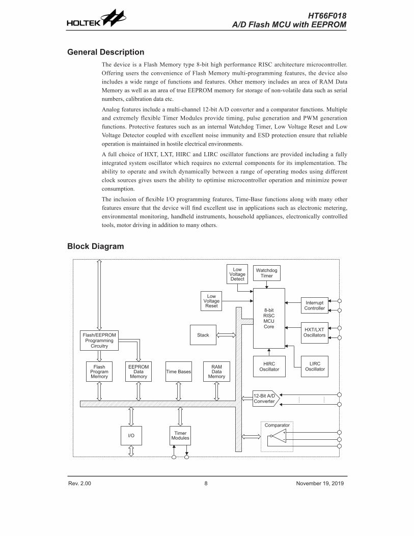
General DescriptionThe device is a Flash Memory type 8-bit high performance RISC architecture microcontroller. Offering users the convenience of Flash Memory multi-programming features, the device also includes a wide range of functions and features. Other memory includes an area of RAM Data Memory as well as an area of true EEPROM memory for storage of non-volatile data such as serial numbers, calibration data etc.
Analog features include a multi-channel 12-bit A/D converter and a comparator functions. Multiple and extremely flexible Timer Modules provide timing, pulse generation and PWM generation functions. Protective features such as an internal Watchdog Timer, Low Voltage Reset and Low Voltage Detector coupled with excellent noise immunity and ESD protection ensure that reliable operation is maintained in hostile electrical environments.
A full choice of HXT, LXT, HIRC and LIRC oscillator functions are provided including a fully integrated system oscillator which requires no external components for its implementation. The ability to operate and switch dynamically between a range of operating modes using different clock sources gives users the ability to optimise microcontroller operation and minimize power consumption.
The inclusion of flexible I/O programming features, Time-Base functions along with many other features ensure that the device will find excellent use in applications such as electronic metering, environmental monitoring, handheld instruments, household appliances, electronically controlled tools, motor driving in addition to many others.
Block Diagram
� � � � � � � � � � � �� � � � � � � � � � �
� � � � � � �
� � � � � �� � � � �
� � � � �� � � �� � �� � � �
� � � � � � � � �� � � � � � � � � �
� � � � � � �� � � � � � � � � �
� � � � � � � �� � � � � � � � �
� � � �� � � � � � � � �
� � � �
� � � � � �� � � �
� � � � �
� � � � �� � � � � � �� � � � �
� � �� � � �
� � � � �
� � � � �� � � � � � �
� � �� � � � � � �� � � � �
� � �� � � � � � �� � � � �
� � � � � � � � � �
� � � � � � � � �
� � �
� � � �� � � � � � � � �
Rev. 2.00 8 November 19, 2019 Rev. 2.00 9 November 19, 2019
HT66F018A/D Flash MCU with EEPROM
HT66F018A/D Flash MCU with EEPROM
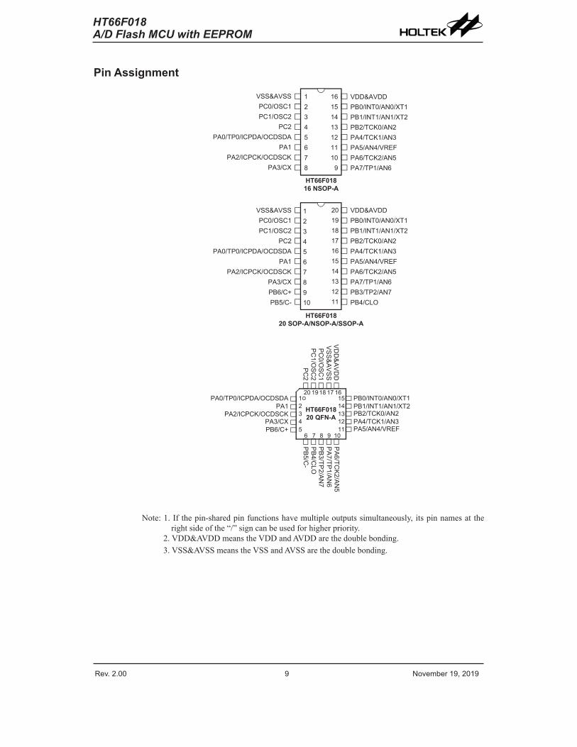
Pin Assignment
VSS&AVSSPC0/OSC1PC1/OSC2
PC2PA0/TP0/ICPDA/OCDSDA
PA1PA2/ICPCK/OCDSCK
PA3/CX
VDD&AVDDPB0/INT0/AN0/XT1PB1/INT1/AN1/XT2PB2/TCK0/AN2PA4/TCK1/AN3PA5/AN4/VREFPA6/TCK2/AN5PA7/TP1/AN6
HT66F01816 NSOP-A
161514131211109
12345678
HT66F01820 SOP-A/NSOP-A/SSOP-A
VSS&AVSSPC0/OSC1PC1/OSC2
PC2PA0/TP0/ICPDA/OCDSDA
PA1PA2/ICPCK/OCDSCK
PA3/CXPB6/C+PB5/C-
VDD&AVDDPB0/INT0/AN0/XT1PB1/INT1/AN1/XT2PB2/TCK0/AN2PA4/TCK1/AN3PA5/AN4/VREFPA6/TCK2/AN5PA7/TP1/AN6PB3/TP2/AN7PB4/CLO
20191817161514131211
12345678910
HT66F01820 QFN-A
6 7 8 9 10
161718192012345
1514131211
PC2
PC1 /O
SC2
PC0/O
SC1
VSS&AVSS
VDD&AVDD
PB1/INT1/AN1/XT2PB2/TCK0/AN2PA4/TCK1/AN3PA5/AN4/VREF
PB0/INT0/AN0/XT1PA1
PA2/ICPCK/OCDSCKPA3/CXPB6/C+
PA0/TP0/ICPDA/OCDSDA
PA6/TC
K2/ AN5
PA7 /TP
1/AN6
PB3/TP
2/AN7
PB4/C
LOPB5/ C
-
Note: 1. If the pin-shared pin functions have multiple outputs simultaneously, its pin names at the right side of the “/” sign can be used for higher priority.
2. VDD&AVDD means the VDD and AVDD are the double bonding.3. VSS&AVSS means the VSS and AVSS are the double bonding.
Rev. 2.00 10 November 19, 2019 Rev. 2.00 11 November 19, 2019
HT66F018A/D Flash MCU with EEPROM
HT66F018A/D Flash MCU with EEPROM
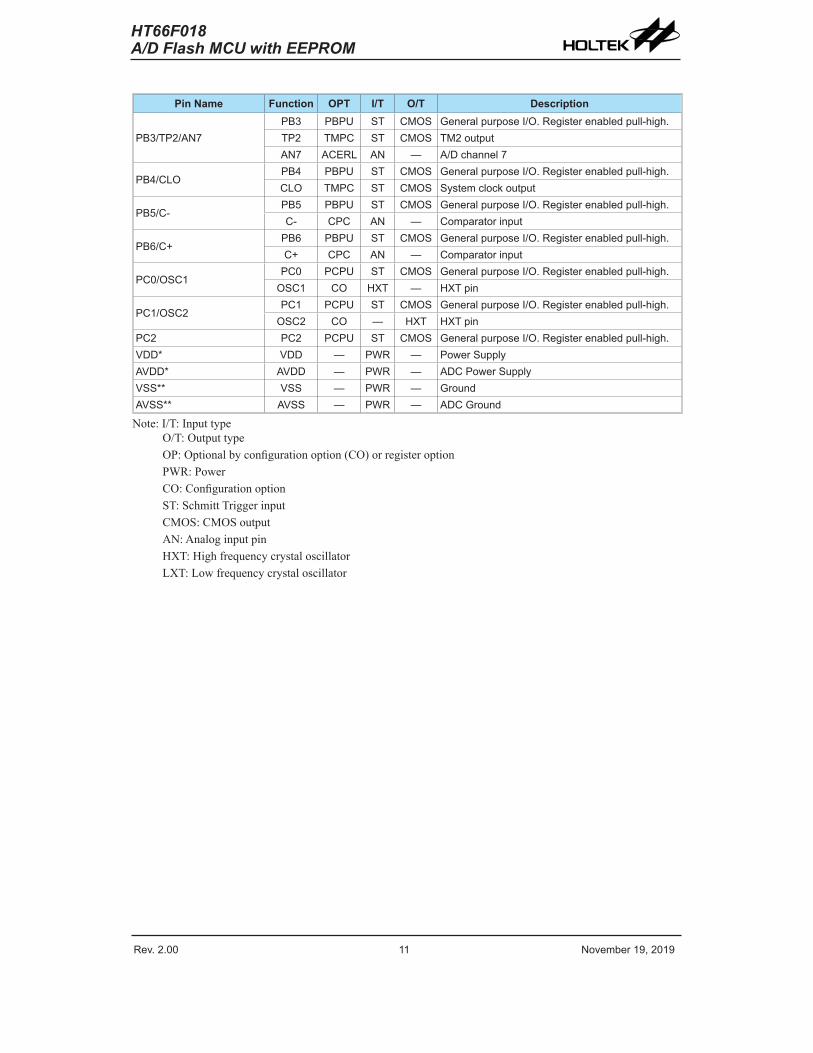
Pin DescriptionWith the exception of the power pins, all pins on the device can be referenced by its Port name, e.g. PA.0, PA.1 etc, which refer to the digital I/O function of the pins. However these Port pins are also shared with other function such as the Analog to Digital Converter, Timer Module pins etc. The function of each pin is listed in the following table, however the details behind how each pin is configured is contained in other sections of the datasheet.
Pin Name Function OPT I/T O/T Description
PA0/TP0/ICPDA/OCDSDA
PA0 PAPUPAWU ST CMOS General purpose I/O. Register enabled pull-high
and wake-up.TP0 TMPC ST CMOS TM0 output
ICPDA — ST CMOS ICP Address/DataOCDSDA — ST CMOS OCDS Address/Data, for EV chip only
PA1 PA1 PAPUPAWU ST CMOS General purpose I/O. Register enabled pull-high
and wake-up.
PA2/ICPCK/OCDSCKPA2 PAPU
PAWU ST CMOS General purpose I/O. Register enabled pull-high and wake-up.
ICPCK — ST — ICP Clock pinOCDSCK — ST — OCDS Clock pin, for EV chip only
PA3/CXPA3 PAPU
PAWU ST CMOS General purpose I/O. Register enabled pull-high and wake-up.
CX CPC — CMOS Comparator output
PA4/TCK1/AN3PA4 PAPU
PAWU ST CMOS General purpose I/O. Register enabled pull-high and wake-up.
TCK1 TM1C0 ST — TM1 inputAN3 ACERL AN — A/D channel 3
PA5/AN4/VREFPA5 PAPU
PAWU ST CMOS General purpose I/O. Register enabled pull-high and wake-up.
AN4 ACERL AN — A/D channel 4VREF ADCR1 AN — ADC reference voltage input pin
PA6/TCK2/AN5PA6 PAPU
PAWU ST CMOS General purpose I/O. Register enabled pull-high and wake-up.
TCK2 TM2C0 ST — TM2 inputAN5 ACERL AN — A/D channel 5
PA7/TP1/AN6PA7 PAPU
PAWU ST CMOS General purpose I/O. Register enabled pull-high and wake-up.
TP1 TMPC ST CMOS TM1 outputAN6 ACERL AN — A/D channel 6
PB0/INT0/AN0/XT1
PB0 PBPU ST CMOS General purpose I/O. Register enabled pull-high.
INT0 INTC0INTEG ST — External Interrupt 0
AN0 ACERL AN — A/D channel 0XT1 CO LXT — Low frequency crystal pin
PB1/INT1/AN1/XT2
PB1 PBPU ST CMOS General purpose I/O. Register enabled pull-high.
INT1 INTC2INTEG ST — External Interrupt 1
AN1 ACERL AN — A/D channel 1XT2 CO — LXT Low frequency crystal pin
PB2/TCK0/AN2PB2 PBPU ST CMOS General purpose I/O. Register enabled pull-high.
TCK0 TM0C0 ST — TM0 inputAN2 ACERL AN — A/D channel 2
Rev. 2.00 10 November 19, 2019 Rev. 2.00 11 November 19, 2019
HT66F018A/D Flash MCU with EEPROM
HT66F018A/D Flash MCU with EEPROM
Pin Name Function OPT I/T O/T Description
PB3/TP2/AN7PB3 PBPU ST CMOS General purpose I/O. Register enabled pull-high.TP2 TMPC ST CMOS TM2 outputAN7 ACERL AN — A/D channel 7
PB4/CLOPB4 PBPU ST CMOS General purpose I/O. Register enabled pull-high.CLO TMPC ST CMOS System clock output
PB5/C-PB5 PBPU ST CMOS General purpose I/O. Register enabled pull-high.C- CPC AN — Comparator input
PB6/C+PB6 PBPU ST CMOS General purpose I/O. Register enabled pull-high.C+ CPC AN — Comparator input
PC0/OSC1PC0 PCPU ST CMOS General purpose I/O. Register enabled pull-high.
OSC1 CO HXT — HXT pin
PC1/OSC2PC1 PCPU ST CMOS General purpose I/O. Register enabled pull-high.
OSC2 CO — HXT HXT pinPC2 PC2 PCPU ST CMOS General purpose I/O. Register enabled pull-high.VDD* VDD — PWR — Power SupplyAVDD* AVDD — PWR — ADC Power SupplyVSS** VSS — PWR — GroundAVSS** AVSS — PWR — ADC Ground
Note: I/T: Input typeO/T: Output typeOP: Optional by configuration option (CO) or register optionPWR: PowerCO: Configuration optionST: Schmitt Trigger inputCMOS: CMOS outputAN: Analog input pinHXT: High frequency crystal oscillatorLXT: Low frequency crystal oscillator
Rev. 2.00 12 November 19, 2019 Rev. 2.00 13 November 19, 2019
HT66F018A/D Flash MCU with EEPROM
HT66F018A/D Flash MCU with EEPROM
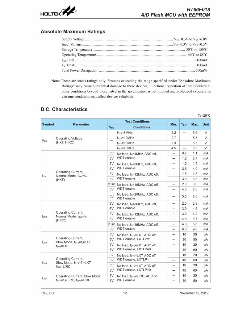
Absolute Maximum RatingsSupply Voltage ................................................................................................VSS−0.3V to VSS+6.0V Input Voltage ..................................................................................................VSS−0.3V to VDD+0.3V Storage Temperature ....................................................................................................-50˚C to 150˚C Operating Temperature ..................................................................................................-40˚C to 85˚C IOH Total ..................................................................................................................................-100mA IOL Total ................................................................................................................................... 100mA Total Power Dissipation ........................................................................................................ 500mW
Note: These are stress ratings only. Stresses exceeding the range specified under "Absolute Maximum Ratings" may cause substantial damage to these devices. Functional operation of these devices at other conditions beyond those listed in the specification is not implied and prolonged exposure to extreme conditions may affect devices reliability.
D.C. CharacteristicsTa=25°C
Symbol ParameterTest Conditions
Min. Typ. Max. UnitVDD Conditions
VDDOperating Voltage(HXT, HIRC) ─
fSYS=8MHz 2.2 ─ 5.5 VfSYS=12MHz 2.7 ─ 5.5 VfSYS=16MHz 3.3 ─ 5.5 VfSYS=20MHz 4.5 ─ 5.5 V
IDD1
Operating Current,Normal Mode, fSYS=fH(HXT)
3V No load, fH=4MHz, ADC off, WDT enable
─ 0.7 1.1 mA5V ─ 1.8 2.7 mA3V No load, fH=8MHz, ADC off,
WDT enable─ 1.0 1.5 mA
5V ─ 2.5 4.0 mA3V No load, fH=12MHz, ADC off,
WDT enable─ 1.5 2.5 mA
5V ─ 3.5 5.5 mA3.3V No load, fH=16MHz, ADC off,
WDT enable─ 2.0 3.0 mA
5V ─ 4.5 7.0 mA
5V No load, fH=20MHz, ADC off, WDT enable ─ 5.5 8.5 mA
IDD2
Operating Current,Normal Mode, fSYS=fH(HIRC)
3V No load, fH=8MHz, ADC off, WDT enable
─ 2.0 2.8 mA5V ─ 3.0 4.5 mA3V No load, fH=12MHz, ADC off,
WDT enable─ 3.0 4.2 mA
5V ─ 4.5 6.7 mA3.3V No load, fH=16MHz, ADC off,
WDT enable─ 4.0 5.6 mA
5V ─ 6.0 9.0 mA
IDD3
Operating Current,Slow Mode, fSYS=fL=LXT, fSUB=LXT
3V No load, fSYS=LXT, ADC off, WDT enable, LXTLP=1
─ 10 20 μA5V ─ 30 50 μA3V No load, fSYS=LXT, ADC off,
WDT enable, LXTLP=0─ 10 20 μA
5V ─ 40 60 μA
IDD4
Operating Current,Slow Mode, fSYS=fL=LXT, fSUB=LIRC
3V No load, fSYS=LXT, ADC off, WDT enable, LXTLP=1
─ 10 20 μA5V ─ 40 60 μA3V No load, fSYS=LXT, ADC off,
WDT enable, LXTLP=0─ 10 20 μA
5V ─ 40 60 μA
IDD5Operating Current, Slow Mode, fSYS=fL=LIRC, fSUB=LIRC
3V No load, fSYS=LIRC, ADC off, WDT enable
─ 10 20 μA5V ─ 30 50 μA
Rev. 2.00 12 November 19, 2019 Rev. 2.00 13 November 19, 2019
HT66F018A/D Flash MCU with EEPROM
HT66F018A/D Flash MCU with EEPROM
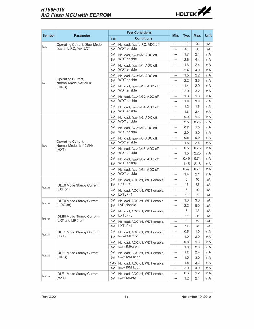
Symbol ParameterTest Conditions
Min. Typ. Max. UnitVDD Conditions
IDD6Operating Current, Slow Mode, fSYS=fL=LIRC, fSUB=LXT
3V No load, fSYS=LIRC, ADC off, WDT enable
─ 10 20 μA5V ─ 40 60 μA
IDD7
Operating Current,Normal Mode, fH=8MHz(HIRC)
3V No load, fSYS=fH/2, ADC off, WDT enable
─ 1.7 2.4 mA5V ─ 2.6 4.4 mA3V No load, fSYS=fH/4, ADC off,
WDT enable─ 1.6 2.4 mA
5V ─ 2.4 4.0 mA3V No load, fSYS=fH/8, ADC off,
WDT enable─ 1.5 2.2 mA
5V ─ 2.2 3.6 mA3V No load, fSYS=fH/16, ADC off,
WDT enable─ 1.4 2.0 mA
5V ─ 2.0 3.2 mA3V No load, fSYS=fH/32, ADC off,
WDT enable─ 1.3 1.8 mA
5V ─ 1.8 2.8 mA3V No load, fSYS=fH/64, ADC off,
WDT enable─ 1.2 1.6 mA
5V ─ 1.6 2.4 mA
IDD8
Operating Current,Normal Mode, fH=12MHz(HXT)
3V No load, fSYS=fH/2, ADC off, WDT enable
─ 0.9 1.5 mA5V ─ 2.5 3.75 mA3V No load, fSYS=fH/4, ADC off,
WDT enable─ 0.7 1.0 mA
5V ─ 2.0 3.0 mA3V No load, fSYS=fH/8, ADC off,
WDT enable─ 0.6 0.9 mA
5V ─ 1.6 2.4 mA3V No load, fSYS=fH/16, ADC off,
WDT enable─ 0.5 0.75 mA
5V ─ 1.5 2.25 mA3V No load, fSYS=fH/32, ADC off,
WDT enable─ 0.49 0.74 mA
5V ─ 1.45 2.18 mA3V No load, fSYS=fH/64, ADC off,
WDT enable─ 0.47 0.71 mA
5V ─ 1.4 2.1 mA
IIDLE01IDLE0 Mode Stanby Current(LXT on)
3V No load, ADC off, WDT enable, LXTLP=0
─ 5 10 μA5V ─ 16 32 μA3V No load, ADC off, WDT enable,
LXTLP=1─ 5 10 μA
5V ─ 16 32 μA
IIDLE02IDLE0 Mode Stanby Current(LIRC on)
3V No load, ADC off, WDT enable, LVR disable
─ 1.3 3.0 μA5V ─ 2.2 5.0 μA
IIDLE03IDLE0 Mode Stanby Current(LXT and LIRC on)
3V No load, ADC off, WDT enable, LXTLP=0
─ 6 12 μA5V ─ 18 36 μA3V No load, ADC off, WDT enable,
LXTLP=1─ 6 12 μA
5V ─ 18 36 μA
IIDLE11IDLE1 Mode Stanby Current(HXT)
3V No load, ADC off, WDT enable, fSYS=8MHz on
─ 0.5 1.0 mA5V ─ 1.0 2.0 mA
IIDLE12IDLE1 Mode Stanby Current(HIRC)
3V No load, ADC off, WDT enable, fSYS=8MHz on
─ 0.8 1.6 mA5V ─ 1.0 2.0 mA3V No load, ADC off, WDT enable,
fSYS=12MHz on─ 1.2 2.4 mA
5V ─ 1.5 3.0 mA3.3V No load, ADC off, WDT enable,
fSYS=16MHz on─ 1.6 3.2 mA
5V ─ 2.0 4.0 mA
IIDLE13IDLE1 Mode Stanby Current(HXT)
3V No load, ADC off, WDT enable, fSYS=12MHz on
─ 0.6 1.2 mA5V ─ 1.2 2.4 mA
Rev. 2.00 14 November 19, 2019 Rev. 2.00 15 November 19, 2019
HT66F018A/D Flash MCU with EEPROM
HT66F018A/D Flash MCU with EEPROM
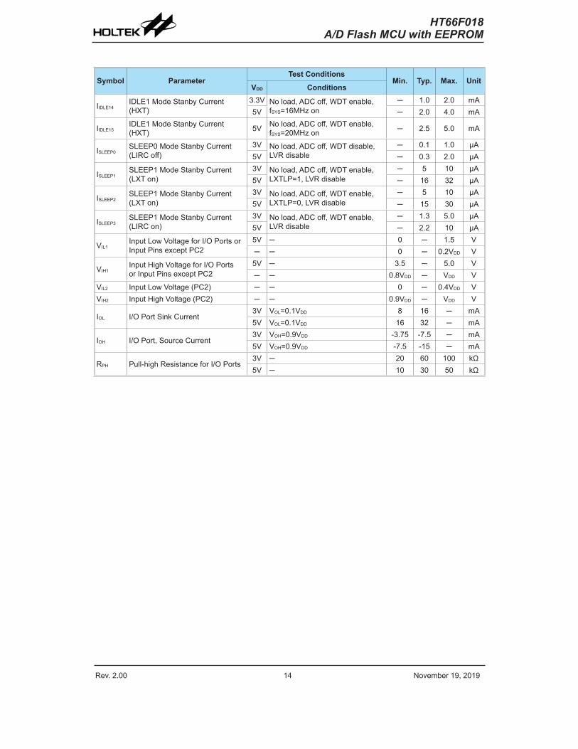
Symbol ParameterTest Conditions
Min. Typ. Max. UnitVDD Conditions
IIDLE14IDLE1 Mode Stanby Current(HXT)
3.3V No load, ADC off, WDT enable, fSYS=16MHz on
─ 1.0 2.0 mA5V ─ 2.0 4.0 mA
IIDLE15IDLE1 Mode Stanby Current(HXT) 5V No load, ADC off, WDT enable,
fSYS=20MHz on ─ 2.5 5.0 mA
ISLEEP0SLEEP0 Mode Stanby Current(LIRC off)
3V No load, ADC off, WDT disable, LVR disable
─ 0.1 1.0 μA5V ─ 0.3 2.0 μA
ISLEEP1SLEEP1 Mode Stanby Current(LXT on)
3V No load, ADC off, WDT enable, LXTLP=1, LVR disable
─ 5 10 μA5V ─ 16 32 μA
ISLEEP2SLEEP1 Mode Stanby Current(LXT on)
3V No load, ADC off, WDT enable, LXTLP=0, LVR disable
─ 5 10 μA5V ─ 15 30 μA
ISLEEP3SLEEP1 Mode Stanby Current(LIRC on)
3V No load, ADC off, WDT enable, LVR disable
─ 1.3 5.0 μA5V ─ 2.2 10 μA
VIL1Input Low Voltage for I/O Ports or Input Pins except PC2
5V ─ 0 ─ 1.5 V─ ─ 0 ─ 0.2VDD V
VIH1Input High Voltage for I/O Portsor Input Pins except PC2
5V ─ 3.5 ─ 5.0 V─ ─ 0.8VDD ─ VDD V
VIL2 Input Low Voltage (PC2) ─ ─ 0 ─ 0.4VDD VVIH2 Input High Voltage (PC2) ─ ─ 0.9VDD ─ VDD V
IOL I/O Port Sink Current3V VOL=0.1VDD 8 16 ─ mA5V VOL=0.1VDD 16 32 ─ mA
IOH I/O Port, Source Current3V VOH=0.9VDD -3.75 -7.5 ─ mA5V VOH=0.9VDD -7.5 -15 ─ mA
RPH Pull-high Resistance for I/O Ports3V ─ 20 60 100 kΩ5V ─ 10 30 50 kΩ
Rev. 2.00 14 November 19, 2019 Rev. 2.00 15 November 19, 2019
HT66F018A/D Flash MCU with EEPROM
HT66F018A/D Flash MCU with EEPROM
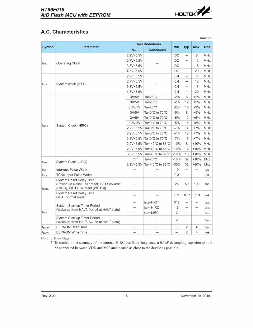
A.C. CharacteristicsTa=25°C
Symbol ParameterTest Conditions
Min. Typ. Max. UnitVDD Conditions
fCPU Operating Clock
2.2V~5.5V
─
DC ─ 8 MHz2.7V~5.5V DC ─ 12 MHz3.3V~5.5V DC ─ 16 MHz4.5V~5.5V DC ─ 20 MHz
fSYS System clock (HXT)
2.2V~5.5V
─
0.4 ─ 8 MHz2.7V~5.5V 0.4 ─ 12 MHz3.3V~5.5V 0.4 ─ 16 MHz4.5V~5.5V 0.4 ─ 20 MHz
fHIRC System Clock (HIRC)
3V/5V Ta=25°C -2% 8 +2% MHz3V/5V Ta=25°C -2% 12 +2% MHz
3.3V/5V Ta=25°C -2% 16 +2% MHz3V/5V Ta=0°C to 70°C -5% 8 +5% MHz3V/5V Ta=0°C to 70°C -5% 12 +5% MHz
3.3V/5V Ta=0°C to 70°C -5% 16 +5% MHz2.2V~5.5V Ta=0°C to 70°C -7% 8 +7% MHz2.2V~5.5V Ta=0°C to 70°C -7% 12 +7% MHz3.3V~5.5V Ta=0°C to 70°C -7% 16 +7% MHz2.2V~5.5V Ta=-40°C to 85°C -10% 8 +10% MHz2.2V~5.5V Ta=-40°C to 85°C -10% 12 +10% MHz3.3V~5.5V Ta=-40°C to 85°C -10% 16 +10% MHz
fLIRC System Clock (LIRC)5V Ta=25°C -10% 32 +10% kHz
2.2V~5.5V Ta=-40°C to 85°C -30% 32 +60% kHztINT Interrupt Pulse Width ─ ─ 10 ─ ─ μstTCK TCKn Input Pulse Width ─ ─ 0.3 ─ ─ μs
tRSTD
System Reset Delay Time(Power On Reset, LVR reset, LVR S/W reset (LVRC), WDT S/W reset (WDTC))
─ ─ 25 50 100 ms
System Reset Delay Time(WDT normal reset) ─ ─ 8.3 16.7 33.3 ms
tSST
System Start-up Timer Period(Wake-up from HALT, fSYS off at HALT state)
─ fSYS=HXT 512 ─ ─ tSYS
─ fSYS=HIRC 16 ─ ─ tSYS
─ fSYS=LIRC 2 ─ ─ tSYS
System Start-up Timer Period(Wake-up from HALT, fSYS on at HALT state) ─ ─ 2 ─ ─ tSYS
tEERD EEPROM Read Time ─ ─ ─ 2 4 tSYS
tEEWR EEPROM Write Time ─ ─ ─ 2 4 ms
Note: 1. tSYS=1/fSYS
2. To maintain the accuracy of the internal HIRC oscillator frequency, a 0.1μF decoupling capacitor should be connected between VDD and VSS and located as close to the device as possible.
Rev. 2.00 16 November 19, 2019 Rev. 2.00 17 November 19, 2019
HT66F018A/D Flash MCU with EEPROM
HT66F018A/D Flash MCU with EEPROM
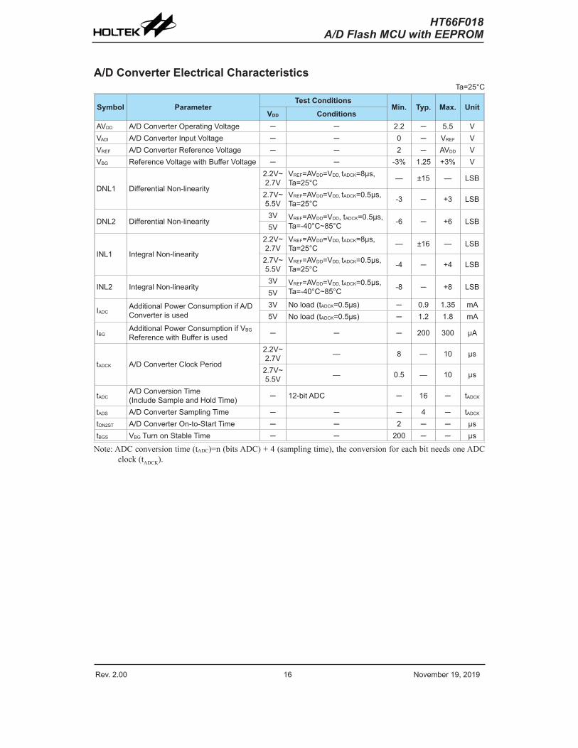
A/D Converter Electrical CharacteristicsTa=25°C
Symbol ParameterTest Conditions
Min. Typ. Max. UnitVDD Conditions
AVDD A/D Converter Operating Voltage ─ ─ 2.2 ─ 5.5 VVADI A/D Converter Input Voltage ─ ─ 0 ─ VREF VVREF A/D Converter Reference Voltage ─ ─ 2 ─ AVDD VVBG Reference Voltage with Buffer Voltage ─ ─ -3% 1.25 +3% V
DNL1 Differential Non-linearity
2.2V~ 2.7V
VREF=AVDD=VDD, tADCK=8μs,Ta=25°C — ±15 — LSB
2.7V~ 5.5V
VREF=AVDD=VDD, tADCK=0.5μs,Ta=25°C -3 ─ +3 LSB
DNL2 Differential Non-linearity3V VREF=AVDD=VDD, tADCK=0.5μs,
Ta=-40°C~85°C -6 ─ +6 LSB5V
INL1 Integral Non-linearity
2.2V~ 2.7V
VREF=AVDD=VDD, tADCK=8μs,Ta=25°C — ±16 — LSB
2.7V~ 5.5V
VREF=AVDD=VDD, tADCK=0.5μs, Ta=25°C -4 ─ +4 LSB
INL2 Integral Non-linearity3V VREF=AVDD=VDD, tADCK=0.5μs,
Ta=-40°C~85°C -8 ─ +8 LSB5V
IADCAdditional Power Consumption if A/D Converter is used
3V No load (tADCK=0.5μs) ─ 0.9 1.35 mA5V No load (tADCK=0.5μs) ─ 1.2 1.8 mA
IBGAdditional Power Consumption if VBG Reference with Buffer is used ─ ─ ─ 200 300 μA
tADCK A/D Converter Clock Period
2.2V~ 2.7V — 8 — 10 μs
2.7V~ 5.5V — 0.5 — 10 μs
tADCA/D Conversion Time(Include Sample and Hold Time) ─ 12-bit ADC ─ 16 ─ tADCK
tADS A/D Converter Sampling Time ─ ─ ─ 4 ─ tADCK
tON2ST A/D Converter On-to-Start Time ─ ─ 2 ─ ─ μstBGS VBG Turn on Stable Time ─ ─ 200 ─ ─ μs
Note: ADC conversion time (tADC)=n (bits ADC) + 4 (sampling time), the conversion for each bit needs one ADC clock (tADCK).

Rev. 2.00 16 November 19, 2019 Rev. 2.00 17 November 19, 2019
HT66F018A/D Flash MCU with EEPROM
HT66F018A/D Flash MCU with EEPROM
LVD&LVR Electrical CharacteristicsTa=25˚C
Symbol ParameterTest Conditions
Min. Typ. Max. UnitVDD Conditions
VLVR1
Low Voltage Reset Voltage —
LVR Enable, 2.10V optio
-5%
2.10
+5%
VVLVR2 LVR Enable, 2.55V option 2.55 VVLVR3 LVR Enable, 3.15V option 3.15 VVLVR4 LVR Enable, 3.80V option 3.80 VVLVD1
Low Voltage Detector Voltage —
LVDEN=1, VLVD=2.0V
-5%
2.00
+5%
VVLVD2 LVDEN=1, VLVD=2.2V 2.20 VVLVD3 LVDEN=1, VLVD=2.4V 2.40 VVLVD4 LVDEN=1, VLVD=2.7V 2.70 VVLVD5 LVDEN=1, VLVD=3.0V 3.00 VVLVD6 LVDEN=1, VLVD=3.3V 3.30 VVLVD7 LVDEN=1, VLVD=3.6V 3.60 VVLVD8 LVDEN=1, VLVD=4.0V 4.00 V
ILVRAdditional Power Consumption if LVR is Used
3VLVR disable → LVR enable
— 30 45 μA5V — 60 90 μA
ILVDAdditional Power Consumption if LVD is Used
3V LVD disable → LVD enable(LVR disable)
— 40 60 μA5V — 75 115 μA3V LVD disable → LVD enable
(LVR enable)— 30 45 μA
5V — 60 90 μAtLVR Low Voltage Width to Reset — — 120 240 480 μStLVD Low Voltage Width to Interrupt — — 20 45 90 μS
tLVDS LVDO stable time — LVD off → LVD on(LVR enable or disable) 15 — — μS
tSRESET Software Reset Width to Reset — — 45 90 120 μS
Comparator Electrical CharacteristicsTa=25°C
Symbol ParameterTest Conditions
Min. Typ. Max. UnitVDD Conditions
VCMP Comparator operating voltage ─ ─ 2.2 ─ 5.5 V
ICMP Comparator operating current3V ─ ─ 37 56 μA5V ─ ─ 130 200 μA
VCMPOS Comparator input offset voltage ─ -10 ─ +10 mVVHYS Hysteresis width ─ 20 40 60 mVVCM Comparator common mode voltage range ─ ─ VSS ─ VDD-1.4V VAOL Comparator open loop gain ─ ─ 60 80 ─ dBtPD Comparator response time ─ With 100mV overdrive(Note) ─ 370 560 ns
Note: Measured with comparator one input pin at VCM=(VDD-1.4)/2 while the other pin input transition from VSS to (VCM+100mV) or from VDD to (VCM-100mV).
Rev. 2.00 18 November 19, 2019 Rev. 2.00 19 November 19, 2019
HT66F018A/D Flash MCU with EEPROM
HT66F018A/D Flash MCU with EEPROM
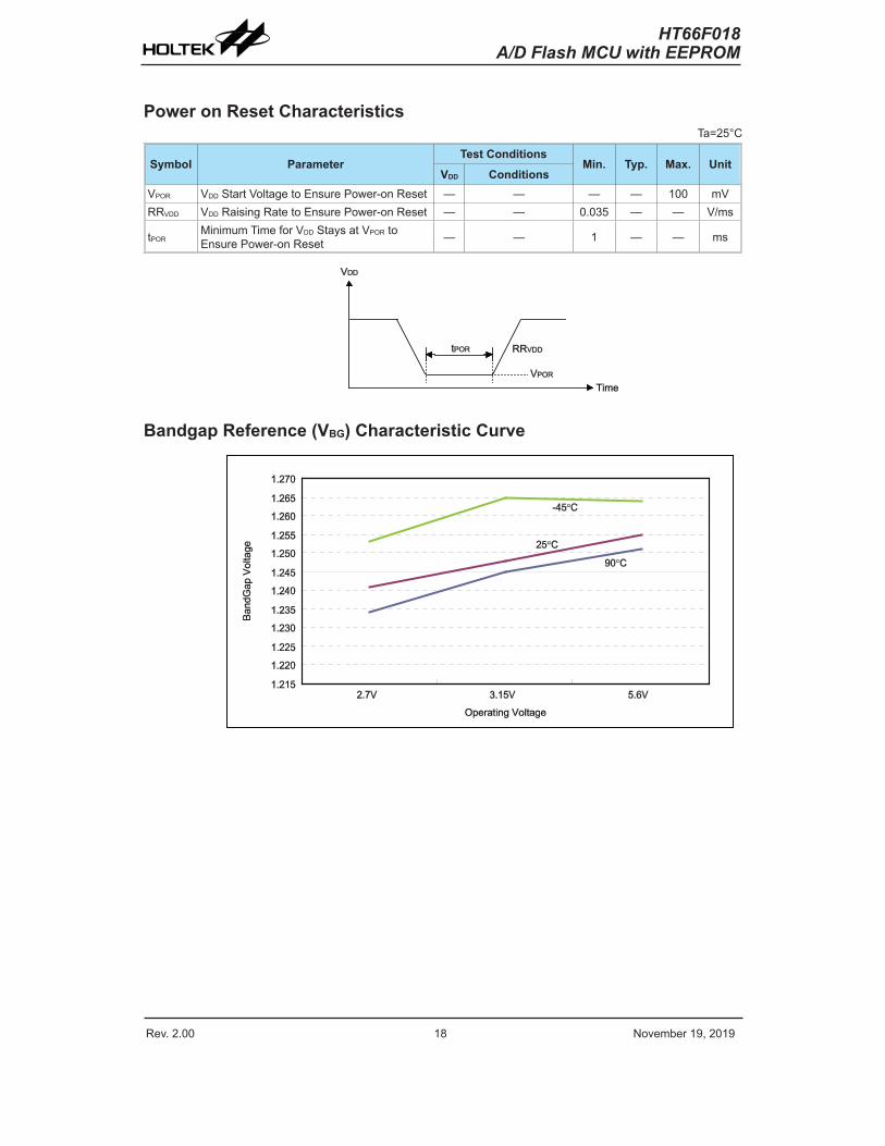
Power on Reset CharacteristicsTa=25°C
Symbol ParameterTest Conditions
Min. Typ. Max. UnitVDD Conditions
VPOR VDD Start Voltage to Ensure Power-on Reset — — — — 100 mVRRVDD VDD Raising Rate to Ensure Power-on Reset — — 0.035 — — V/ms
tPORMinimum Time for VDD Stays at VPOR to Ensure Power-on Reset — — 1 — — ms
Bandgap Reference (VBG) Characteristic Curve
Rev. 2.00 18 November 19, 2019 Rev. 2.00 19 November 19, 2019
HT66F018A/D Flash MCU with EEPROM
HT66F018A/D Flash MCU with EEPROM
System ArchitectureA key factor in the high-performance features of the Holtek range of microcontrollers is attributed to their internal system architecture. The range of the device take advantage of the usual features found within RISC microcontrollers providing increased speed of operation and enhanced performance. The pipelining scheme is implemented in such a way that instruction fetching and instruction execution are overlapped, hence instructions are effectively executed in one cycle, with the exception of branch or call instructions. An 8-bit wide ALU is used in practically all instruction set operations, which carries out arithmetic operations, logic operations, rotation, increment, decrement, branch decisions, etc. The internal data path is simplified by moving data through the Accumulator and the ALU. Certain internal registers are implemented in the Data Memory and can be directly or indirectly addressed. The simple addressing methods of these registers along with additional architectural features ensure that a minimum of external components is required to provide a functional I/O and A/D control system with maximum reliability and flexibility. This makes the device suitable for low-cost, high-volume production for controller applications.
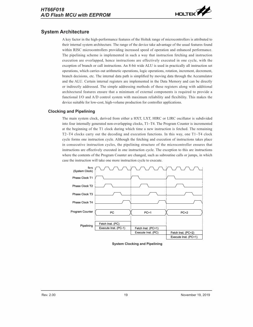
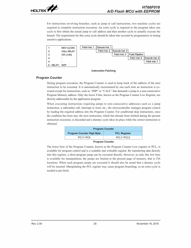
Clocking and PipeliningThe main system clock, derived from either a HXT, LXT, HIRC or LIRC oscillator is subdivided into four internally generated non-overlapping clocks, T1~T4. The Program Counter is incremented at the beginning of the T1 clock during which time a new instruction is fetched. The remaining T2~T4 clocks carry out the decoding and execution functions. In this way, one T1~T4 clock cycle forms one instruction cycle. Although the fetching and execution of instructions takes place in consecutive instruction cycles, the pipelining structure of the microcontroller ensures that instructions are effectively executed in one instruction cycle. The exception to this are instructions where the contents of the Program Counter are changed, such as subroutine calls or jumps, in which case the instruction will take one more instruction cycle to execute.
System Clocking and Pipelining
Rev. 2.00 20 November 19, 2019 Rev. 2.00 21 November 19, 2019
HT66F018A/D Flash MCU with EEPROM
HT66F018A/D Flash MCU with EEPROM
For instructions involving branches, such as jump or call instructions, two machine cycles are required to complete instruction execution. An extra cycle is required as the program takes one cycle to first obtain the actual jump or call address and then another cycle to actually execute the branch. The requirement for this extra cycle should be taken into account by programmers in timing sensitive applications.
Instruction Fetching
Program CounterDuring program execution, the Program Counter is used to keep track of the address of the next instruction to be executed. It is automatically incremented by one each time an instruction is ex-ecuted except for instructions, such as “JMP” or “CALL” that demands a jump to a non-consecutive Program Memory address. Only the lower 8 bits, known as the Program Counter Low Register, are directly addressable by the application program.
When executing instructions requiring jumps to non-consecutive addresses such as a jump instruction, a subroutine call, interrupt or reset, etc., the microcontroller manages program control by loading the required address into the Program Counter. For conditional skip instructions, once the condition has been met, the next instruction, which has already been fetched during the present instruction execution, is discarded and a dummy cycle takes its place while the correct instruction is obtained.
Program CounterProgram Counter High Byte PCL Register
PC11~PC8 PCL7~PCL0Program Counter
The lower byte of the Program Counter, known as the Program Counter Low register or PCL, is available for program control and is a readable and writeable register. By transferring data directly into this register, a short program jump can be executed directly. However, as only this low byte is available for manipulation, the jumps are limited to the present page of memory, that is 256 locations. When such program jumps are executed it should also be noted that a dummy cycle will be inserted. Manipulating the PCL register may cause program branching, so an extra cycle is needed to pre-fetch.
Rev. 2.00 20 November 19, 2019 Rev. 2.00 21 November 19, 2019
HT66F018A/D Flash MCU with EEPROM
HT66F018A/D Flash MCU with EEPROM
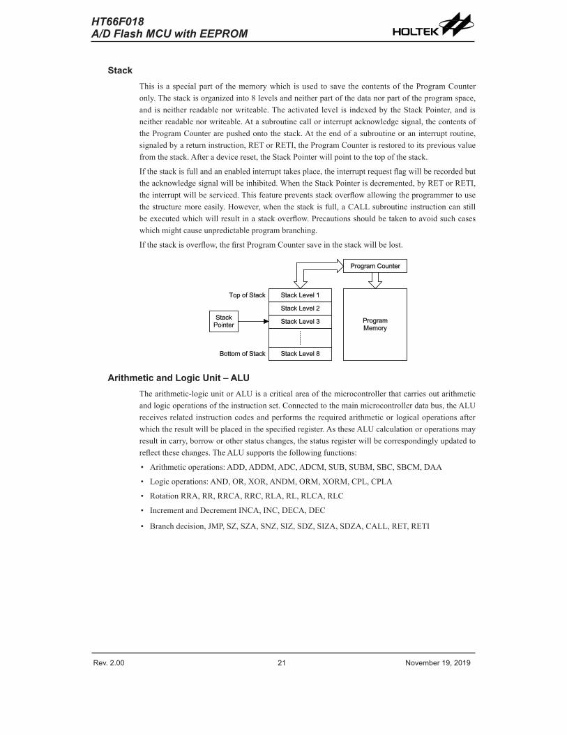
StackThis is a special part of the memory which is used to save the contents of the Program Counter only. The stack is organized into 8 levels and neither part of the data nor part of the program space, and is neither readable nor writeable. The activated level is indexed by the Stack Pointer, and is neither readable nor writeable. At a subroutine call or interrupt acknowledge signal, the contents of the Program Counter are pushed onto the stack. At the end of a subroutine or an interrupt routine, signaled by a return instruction, RET or RETI, the Program Counter is restored to its previous value from the stack. After a device reset, the Stack Pointer will point to the top of the stack.
If the stack is full and an enabled interrupt takes place, the interrupt request flag will be recorded but the acknowledge signal will be inhibited. When the Stack Pointer is decremented, by RET or RETI, the interrupt will be serviced. This feature prevents stack overflow allowing the programmer to use the structure more easily. However, when the stack is full, a CALL subroutine instruction can still be executed which will result in a stack overflow. Precautions should be taken to avoid such cases which might cause unpredictable program branching.
If the stack is overflow, the first Program Counter save in the stack will be lost.
Arithmetic and Logic Unit – ALUThe arithmetic-logic unit or ALU is a critical area of the microcontroller that carries out arithmetic and logic operations of the instruction set. Connected to the main microcontroller data bus, the ALU receives related instruction codes and performs the required arithmetic or logical operations after which the result will be placed in the specified register. As these ALU calculation or operations may result in carry, borrow or other status changes, the status register will be correspondingly updated to reflect these changes. The ALU supports the following functions:
• Arithmetic operations: ADD, ADDM, ADC, ADCM, SUB, SUBM, SBC, SBCM, DAA
• Logic operations: AND, OR, XOR, ANDM, ORM, XORM, CPL, CPLA
• Rotation RRA, RR, RRCA, RRC, RLA, RL, RLCA, RLC
• Increment and Decrement INCA, INC, DECA, DEC
• Branch decision, JMP, SZ, SZA, SNZ, SIZ, SDZ, SIZA, SDZA, CALL, RET, RETI
Rev. 2.00 22 November 19, 2019 Rev. 2.00 23 November 19, 2019
HT66F018A/D Flash MCU with EEPROM
HT66F018A/D Flash MCU with EEPROM
Flash Program MemoryThe Program Memory is the location where the user code or program is stored. For this device series the Program Memory is Flash type, which means it can be programmed and re-programmed a large number of times, allowing the user the convenience of code modification on the same device. By using the appropriate programming tools, the Flash device offer users the flexibility to conveniently debug and develop their applications while also offering a means of field programming and updating.
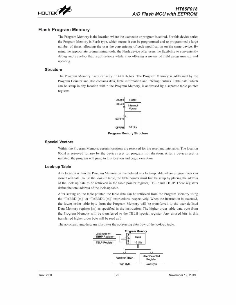
StructureThe Program Memory has a capacity of 4K×16 bits. The Program Memory is addressed by the Program Counter and also contains data, table information and interrupt entries. Table data, which can be setup in any location within the Program Memory, is addressed by a separate table pointer register.
Program Memory Structure
Special VectorsWithin the Program Memory, certain locations are reserved for the reset and interrupts. The location 000H is reserved for use by the device reset for program initialisation. After a device reset is initiated, the program will jump to this location and begin execution.
Look-up TableAny location within the Program Memory can be defined as a look-up table where programmers can store fixed data. To use the look-up table, the table pointer must first be setup by placing the address of the look up data to be retrieved in the table pointer register, TBLP and TBHP. These registers define the total address of the look-up table.
After setting up the table pointer, the table data can be retrieved from the Program Memory using the “TABRD [m]” or “TABRDL [m]” instructions, respectively. When the instruction is executed, the lower order table byte from the Program Memory will be transferred to the user defined Data Memory register [m] as specified in the instruction. The higher order table data byte from the Program Memory will be transferred to the TBLH special register. Any unused bits in this transferred higher order byte will be read as 0.
The accompanying diagram illustrates the addressing data flow of the look-up table.
Rev. 2.00 22 November 19, 2019 Rev. 2.00 23 November 19, 2019
HT66F018A/D Flash MCU with EEPROM
HT66F018A/D Flash MCU with EEPROM
Table Program ExampleThe following example shows how the table pointer and table data is defined and retrieved from the microcontroller. This example uses raw table data located in the Program Memory which is stored there using the ORG statement. The value at this ORG statement is “F00H” which refers to the start address of the last page within the 4K Program Memory of the microcontroller. The table pointer is setup here to have an initial value of “06H”. This will ensure that the first data read from the data table will be at the Program Memory address “F06H” or 6 locations after the start of the last page. Note that the value for the table pointer is referenced to the first address of the present page if the “TABRD [m]” instruction is being used. The high byte of the table data which in this case is equal to zero will be transferred to the TBLH register automatically when the “TABRD [m]” instruction is executed.
Because the TBLH register is a read-only register and cannot be restored, care should be taken to ensure its protection if both the main routine and Interrupt Service Routine use table read instructions. If using the table read instructions, the Interrupt Service Routines may change the value of the TBLH and subsequently cause errors if used again by the main routine. As a rule it is recommended that simultaneous use of the table read instructions should be avoided. However, in situations where simultaneous use cannot be avoided, the interrupts should be disabled prior to the execution of any main routine table-read instructions. Note that all table related instructions require two instruction cycles to complete their operation.
Table Read Program Exampletempreg1 db ? ; temporary register #1tempreg2 db ? ; temporary register #2:mov a, 06h ; initialise low table pointer - note that this addressmov tblp, a ; is referencedmov a, 0Fh ; initialise high table pointermov tbhp, a:tabrd tempreg1 ; transfers value in table referenced by table pointer data at ; program memory address F06H transferred to tempreg1 and TBLHdec tblp ; reduce value of table pointer by onetabrd tempreg2 ; transfers value in table referenced by table pointer data at ; program memory address F05H transferred to tempreg2 and TBLH ; in this example the data 1AH is transferred to tempreg1 and ; data 0FH to register tempreg2:org F00h ; sets initial address of program memorydc 00Ah, 00Bh, 00Ch, 00Dh, 00Eh, 00Fh, 01Ah, 01Bh:
Rev. 2.00 24 November 19, 2019 Rev. 2.00 25 November 19, 2019
HT66F018A/D Flash MCU with EEPROM
HT66F018A/D Flash MCU with EEPROM
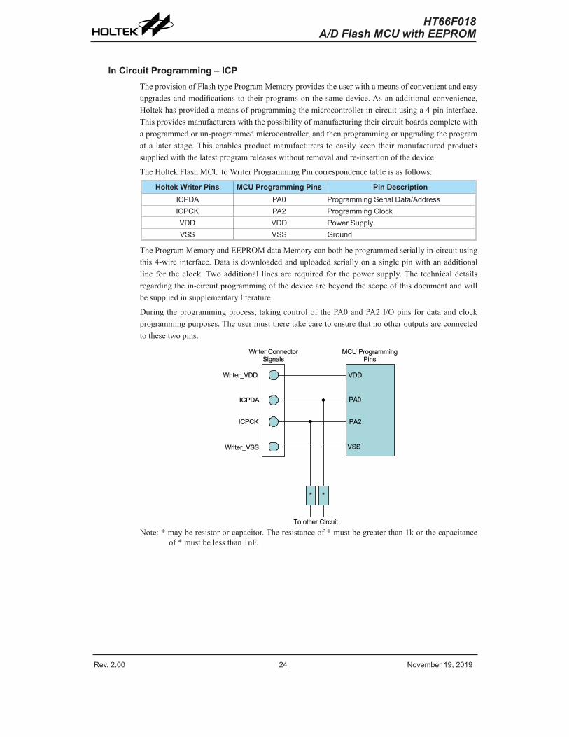
In Circuit Programming – ICPThe provision of Flash type Program Memory provides the user with a means of convenient and easy upgrades and modifications to their programs on the same device. As an additional convenience, Holtek has provided a means of programming the microcontroller in-circuit using a 4-pin interface. This provides manufacturers with the possibility of manufacturing their circuit boards complete with a programmed or un-programmed microcontroller, and then programming or upgrading the program at a later stage. This enables product manufacturers to easily keep their manufactured products supplied with the latest program releases without removal and re-insertion of the device.
The Holtek Flash MCU to Writer Programming Pin correspondence table is as follows:
Holtek Writer Pins MCU Programming Pins Pin DescriptionICPDA PA0 Programming Serial Data/AddressICPCK PA2 Programming ClockVDD VDD Power SupplyVSS VSS Ground
The Program Memory and EEPROM data Memory can both be programmed serially in-circuit using this 4-wire interface. Data is downloaded and uploaded serially on a single pin with an additional line for the clock. Two additional lines are required for the power supply. The technical details regarding the in-circuit programming of the device are beyond the scope of this document and will be supplied in supplementary literature.
During the programming process, taking control of the PA0 and PA2 I/O pins for data and clock programming purposes. The user must there take care to ensure that no other outputs are connected to these two pins.
Note: * may be resistor or capacitor. The resistance of * must be greater than 1k or the capacitance of * must be less than 1nF.
Rev. 2.00 24 November 19, 2019 Rev. 2.00 25 November 19, 2019
HT66F018A/D Flash MCU with EEPROM
HT66F018A/D Flash MCU with EEPROM
On-Chip Debug Support — OCDSAn EV chip exists for the purposes of device emulation. This EV chip device also provides an “On-Chip Debug” function to debug the device during the development process. The EV chip and the actual MCU devices are almost functionally compatible except for the “On-Chip Debug” function. Users can use the EV chip device to emulate the real chip device behavior by connecting the OCDSDA and OCDSCK pins to the Holtek HT-IDE development tools. The OCDSDA pin is the OCDS Data/Address input/output pin while the OCDSCK pin is the OCDS clock input pin. When users use the EV chip for debugging, other functions which are shared with the OCDSDA and OCDSCK pins in the actual MCU device will have no effect in the EV chip. However, the two OCDS pins which are pin-shared with the ICP programming pins are still used as the Flash Memory programming pins for ICP. For a more detailed OCDS description, refer to the corresponding document named “Holtek e-Link for 8-bit MCU OCDS User’s Guide”.
Holtek e-Link Pins EV Chip Pins Pin DescriptionOCDSDA OCDSDA On-chip Debug Support Data/Address input/outputOCDSCK OCDSCK On-chip Debug Support Clock input
VDD VDD Power SupplyGND VSS Ground
Rev. 2.00 26 November 19, 2019 Rev. 2.00 27 November 19, 2019
HT66F018A/D Flash MCU with EEPROM
HT66F018A/D Flash MCU with EEPROM
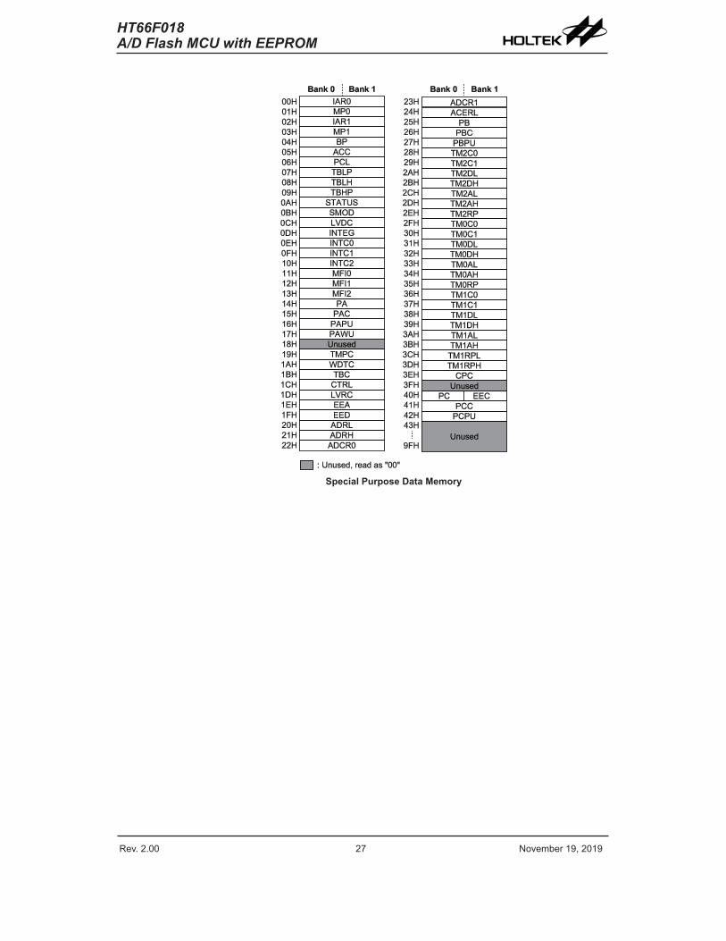
RAM Data MemoryThe Data Memory is a volatile area of 8-bit wide RAM internal memory and is the location where temporary information is stored.
StructureDivided into two banks, the first of these is an area of RAM, known as the Special Function Data Memory. Here are located registers which are necessary for correct operation of the device. Many of these registers can be read from and written to directly under program control, however, some remain protected from user manipulation. The second area of Data Memory is known as the General Purpose Data Memory, which is reserved for general purpose use. All locations within this area are read and write accessible under program control.
The overall Data Memory is subdivided into two banks. The Special Purpose Data Memory registers are accessible in all banks, with the exception of the EEC register at address 40H, which is only accessible in Bank 1. Switching between the different Data Memory banks is achieved by setting the Bank Pointer to the correct value. The start address of the Data Memory for the device is the address 00H.
Capacity Banks
192×8 0: A0H~FFH1: A0H~FFH
General Purpose Data Memory
Rev. 2.00 26 November 19, 2019 Rev. 2.00 27 November 19, 2019
HT66F018A/D Flash MCU with EEPROM
HT66F018A/D Flash MCU with EEPROM
Special Purpose Data Memory
Rev. 2.00 28 November 19, 2019 Rev. 2.00 29 November 19, 2019
HT66F018A/D Flash MCU with EEPROM
HT66F018A/D Flash MCU with EEPROM
Special Function Register DescriptionMost of the Special Function Register details will be described in the relevant functional sections; however several registers require a separate description in this section.
Indirect Addressing Register – IAR0, IAR1The Indirect Addressing Registers, IAR0 and IAR1, although having their locations in normal RAM register space, do not actually physically exist as normal registers. The method of indirect addressing for RAM data manipulation uses these Indirect Addressing Registers and Memory Pointers, in contrast to direct memory addressing, where the actual memory address is specified. Actions on the IAR0 and IAR1 registers will result in no actual read or write operation to these registers but rather to the memory location specified by their corresponding Memory Pointers, MP0 or MP1. Acting as a pair, IAR0 and MP0 can together access data from Bank 0 while the IAR1 and MP1 register pair can access data from any bank. As the Indirect Addressing Registers are not physically implemented, reading the Indirect Addressing Registers indirectly will return a result of “00H” and writing to the registers indirectly will result in no operation.
Memory Pointers – MP0, MP1 Two Memory Pointers, known as MP0 and MP1 are provided. These Memory Pointers are physically implemented in the Data Memory and can be manipulated in the same way as normal registers providing a convenient way with which to address and track data. When any operation to the relevant Indirect Addressing Registers is carried out, the actual address that the microcontroller is directed to, is the address specified by the related Memory Pointer. MP0, together with Indirect Addressing Register, IAR0, are used to access data from Bank 0, while MP1 and IAR1 are used to access data from all banks according to BP register. Direct Addressing can only be used with Bank 0, all other Banks must be addressed indirectly using MP1 and IAR1.
The following example shows how to clear a section of four Data Memory locations already defined as locations adres1 to adres4.
Indirect Addressing Program Exampledata .section ‘data’adres1 db ?adres2 db ?adres3 db ?adres4 db ?block db ?code .section at 0 codeorg 00hstart:mov a, 04h ; setup size of blockmov block, amov a, offset adres1 ; Accumulator loaded with first RAM addressmov mp0, a ; setup memory pointer with first RAM addressloop: clr IAR0 ; clear the data at address defined by MP0inc mp0 ; increment memory pointersdz block ; check if last memory location has been clearedjmp loopcontinue:
The important point to note here is that in the example shown above, no reference is made to specific Data Memory addresses.
Rev. 2.00 28 November 19, 2019 Rev. 2.00 29 November 19, 2019
HT66F018A/D Flash MCU with EEPROM
HT66F018A/D Flash MCU with EEPROM
Bank Pointer – BP For this device, the Data Memory is divided into two banks, Bank0 and Bank1. Selecting the required Data Memory area is achieved using the Bank Pointer. Bit 0 of the Bank Pointer is used to select Data Memory Banks 0~1.
The Data Memory is initialised to Bank 0 after a reset, except for a WDT time-out reset in the Power Down Mode, in which case, the Data Memory bank remains unaffected. It should be noted that the Special Function Data Memory is not affected by the bank selection, which means that the Special Function Registers can be accessed from within any bank. Directly addressing the Data Memory will always result in Bank 0 being accessed irrespective of the value of the Bank Pointer. Accessing data from Bank1 must be implemented using Indirect Addressing.
BP RegisterBit 7 6 5 4 3 2 1 0
Name — — — — — — — DMBP0R/W — — — — — — — R/WPOR — — — — — — — 0
Bit 7~1 Unimplemented, read as “0”Bit 0 DMBP0: Select Data Memory Banks
0: Bank 01: Bank 1
Accumulator – ACCThe Accumulator is central to the operation of any microcontroller and is closely related with operations carried out by the ALU. The Accumulator is the place where all intermediate results from the ALU are stored. Without the Accumulator it would be necessary to write the result of each calculation or logical operation such as addition, subtraction, shift, etc., to the Data Memory resulting in higher programming and timing overheads. Data transfer operations usually involve the temporary storage function of the Accumulator; for example, when transferring data between one user defined register and another, it is necessary to do this by passing the data through the Accumulator as no direct transfer between two registers is permitted.
Program Counter Low Register – PCL To provide additional program control functions, the low byte of the Program Counter is made accessible to programmers by locating it within the Special Purpose area of the Data Memory. By manipulating this register, direct jumps to other program locations are easily implemented. Loading a value directly into this PCL register will cause a jump to the specified Program Memory location, however, as the register is only 8-bit wide, only jumps within the current Program Memory page are permitted. When such operations are used, note that a dummy cycle will be inserted.
Look-up Table Registers – TBLP, TBHP, TBLH These three special function registers are used to control operation of the look-up table which is stored in the Program Memory. TBLP and TBHP are the table pointers and indicate the location where the table data is located. Their value must be setup before any table read commands are executed. Their value can be changed, for example using the “INC” or “DEC” instructions, allowing for easy table data pointing and reading. TBLH is the location where the high order byte of the table data is stored after a table read data instruction has been executed. Note that the lower order table data byte is transferred to a user defined location.
Rev. 2.00 30 November 19, 2019 Rev. 2.00 31 November 19, 2019
HT66F018A/D Flash MCU with EEPROM
HT66F018A/D Flash MCU with EEPROM
Status Register – STATUS This 8-bit register contains the zero flag (Z), carry flag (C), auxiliary carry flag (AC), overflow flag (OV), power down flag (PDF), and watchdog time-out flag (TO). These arithmetic/logical operation and system management flags are used to record the status and operation of the microcontroller.
With the exception of the TO and PDF flags, bits in the status register can be altered by instructions like most other registers. Any data written into the status register will not change the TO or PDF flag. In addition, operations related to the status register may give different results due to the different instruction operations. The TO flag can be affected only by a system power-up, a WDT time-out or by executing the “CLR WDT” or “HALT” instruction. The PDF flag is affected only by executing the “HALT” or “CLR WDT” instruction or during a system power-up.
The Z, OV, AC and C flags generally reflect the status of the latest operations.
• C is set if an operation results in a carry during an addition operation or if a borrow does not take place during a subtraction operation; otherwise C is cleared. C is also affected by a rotate through carry instruction.
• AC is set if an operation results in a carry out of the low nibbles in addition, or no borrow from the high nibble into the low nibble in subtraction; otherwise AC is cleared.
• Z is set if the result of an arithmetic or logical operation is zero; otherwise Z is cleared.
• OV is set if an operation results in a carry into the highest-order bit but not a carry out of the highest-order bit, or vice versa; otherwise OV is cleared.
• PDF is cleared by a system power-up or executing the “CLR WDT” instruction. PDF is set by executing the “HALT” instruction.
• TO is cleared by a system power-up or executing the “CLR WDT” or “HALT” instruction. TO is set by a WDT time-out.
In addition, on entering an interrupt sequence or executing a subroutine call, the status register will not be pushed onto the stack automatically. If the contents of the status registers are important and if the subroutine can corrupt the status register, precautions must be taken to correctly save it.

Rev. 2.00 30 November 19, 2019 Rev. 2.00 31 November 19, 2019
HT66F018A/D Flash MCU with EEPROM
HT66F018A/D Flash MCU with EEPROM
STATUS RegisterBit 7 6 5 4 3 2 1 0
Name — — TO PDF OV Z AC CR/W — — R R R/W R/W R/W R/WPOR — — 0 0 x x x x
“x” unknownBit 7~6 Unimplemented, read as “0”Bit 5 TO: Watchdog Time-Out flag
0: After power up or executing the “CLR WDT” or “HALT” instruction1: A watchdog time-out occurred.
Bit 4 PDF: Power down flag0: After power up or executing the “CLR WDT” instruction1: By executing the “HALT” instruction
Bit 3 OV: Overflow flag0: No overflow1: An operation results in a carry into the highest-order bit but not a carry out of the
highest-order bit or vice versa.Bit 2 Z: Zero flag
0: The result of an arithmetic or logical operation is not zero1: The result of an arithmetic or logical operation is zero
Bit 1 AC: Auxiliary flag0: No auxiliary carry1: An operation results in a carry out of the low nibbles in addition, or no borrow
from the high nibble into the low nibble in subtractionBit 0 C: Carry flag
0: No carry-out1: An operation results in a carry during an addition operation or if a borrow does
not take place during a subtraction operation C is also affected by a rotate through carry instruction.
Rev. 2.00 32 November 19, 2019 Rev. 2.00 33 November 19, 2019
HT66F018A/D Flash MCU with EEPROM
HT66F018A/D Flash MCU with EEPROM
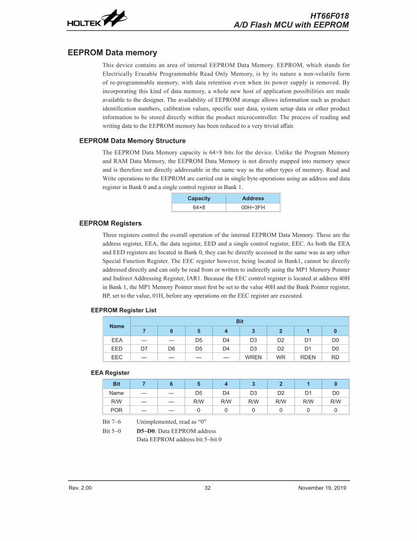
EEPROM Data memoryThis device contains an area of internal EEPROM Data Memory. EEPROM, which stands for Electrically Erasable Programmable Read Only Memory, is by its nature a non-volatile form of re-programmable memory, with data retention even when its power supply is removed. By incorporating this kind of data memory, a whole new host of application possibilities are made available to the designer. The availability of EEPROM storage allows information such as product identification numbers, calibration values, specific user data, system setup data or other product information to be stored directly within the product microcontroller. The process of reading and writing data to the EEPROM memory has been reduced to a very trivial affair.
EEPROM Data Memory StructureThe EEPROM Data Memory capacity is 64×8 bits for the device. Unlike the Program Memory and RAM Data Memory, the EEPROM Data Memory is not directly mapped into memory space and is therefore not directly addressable in the same way as the other types of memory. Read and Write operations to the EEPROM are carried out in single byte operations using an address and data register in Bank 0 and a single control register in Bank 1.
Capacity Address64×8 00H~3FH
EEPROM RegistersThree registers control the overall operation of the internal EEPROM Data Memory. These are the address register, EEA, the data register, EED and a single control register, EEC. As both the EEA and EED registers are located in Bank 0, they can be directly accessed in the same was as any other Special Function Register. The EEC register however, being located in Bank1, cannot be directly addressed directly and can only be read from or written to indirectly using the MP1 Memory Pointer and Indirect Addressing Register, IAR1. Because the EEC control register is located at address 40H in Bank 1, the MP1 Memory Pointer must first be set to the value 40H and the Bank Pointer register, BP, set to the value, 01H, before any operations on the EEC register are executed.
EEPROM Register List
NameBit
7 6 5 4 3 2 1 0EEA — — D5 D4 D3 D2 D1 D0EED D7 D6 D5 D4 D3 D2 D1 D0EEC — — — — WREN WR RDEN RD
EEA RegisterBit 7 6 5 4 3 2 1 0
Name — — D5 D4 D3 D2 D1 D0R/W — — R/W R/W R/W R/W R/W R/WPOR — — 0 0 0 0 0 0
Bit 7~6 Unimplemented, read as “0”Bit 5~0 D5~D0: Data EEPROM address
Data EEPROM address bit 5~bit 0
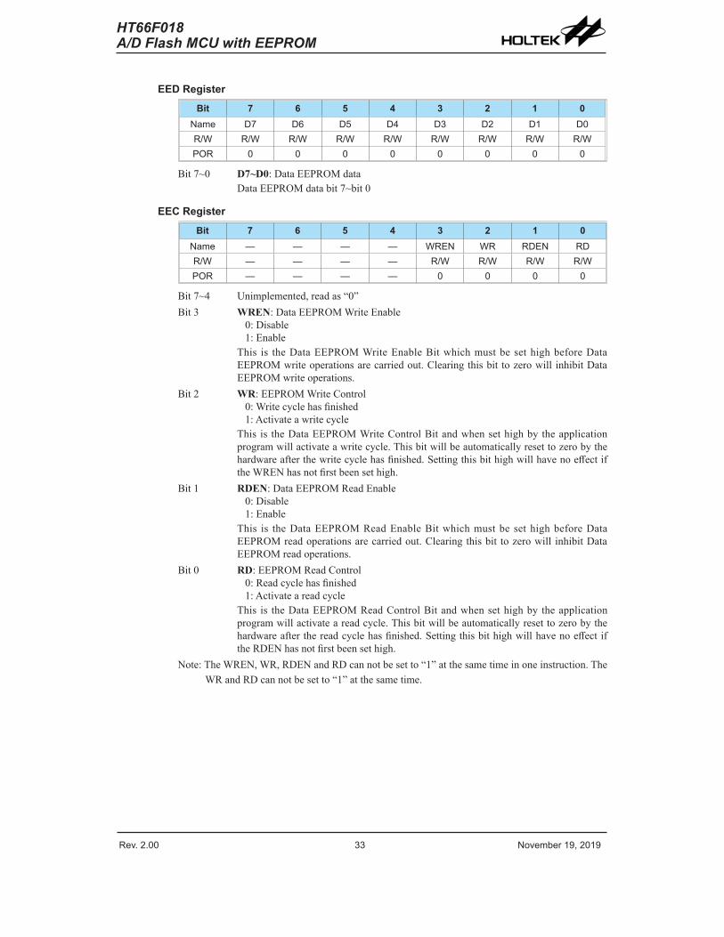
Rev. 2.00 32 November 19, 2019 Rev. 2.00 33 November 19, 2019
HT66F018A/D Flash MCU with EEPROM
HT66F018A/D Flash MCU with EEPROM
EED RegisterBit 7 6 5 4 3 2 1 0
Name D7 D6 D5 D4 D3 D2 D1 D0R/W R/W R/W R/W R/W R/W R/W R/W R/WPOR 0 0 0 0 0 0 0 0
Bit 7~0 D7~D0: Data EEPROM dataData EEPROM data bit 7~bit 0
EEC RegisterBit 7 6 5 4 3 2 1 0
Name — — — — WREN WR RDEN RDR/W — — — — R/W R/W R/W R/WPOR — — — — 0 0 0 0
Bit 7~4 Unimplemented, read as “0”Bit 3 WREN: Data EEPROM Write Enable
0: Disable1: Enable
This is the Data EEPROM Write Enable Bit which must be set high before Data EEPROM write operations are carried out. Clearing this bit to zero will inhibit Data EEPROM write operations.
Bit 2 WR: EEPROM Write Control0: Write cycle has finished1: Activate a write cycle
This is the Data EEPROM Write Control Bit and when set high by the application program will activate a write cycle. This bit will be automatically reset to zero by the hardware after the write cycle has finished. Setting this bit high will have no effect if the WREN has not first been set high.
Bit 1 RDEN: Data EEPROM Read Enable0: Disable1: Enable
This is the Data EEPROM Read Enable Bit which must be set high before Data EEPROM read operations are carried out. Clearing this bit to zero will inhibit Data EEPROM read operations.
Bit 0 RD: EEPROM Read Control0: Read cycle has finished1: Activate a read cycle
This is the Data EEPROM Read Control Bit and when set high by the application program will activate a read cycle. This bit will be automatically reset to zero by the hardware after the read cycle has finished. Setting this bit high will have no effect if the RDEN has not first been set high.
Note: The WREN, WR, RDEN and RD can not be set to “1” at the same time in one instruction. The WR and RD can not be set to “1” at the same time.
Rev. 2.00 34 November 19, 2019 Rev. 2.00 35 November 19, 2019
HT66F018A/D Flash MCU with EEPROM
HT66F018A/D Flash MCU with EEPROM
Reading Data from the EEPROMTo read data from the EEPROM, the read enable bit, RDEN, in the EEC register must first be set high to enable the read function. The EEPROM address of the data to be read must then be placed in the EEA register. If the RD bit in the EEC register is now set high, a read cycle will be initiated. Setting the RD bit high will not initiate a read operation if the RDEN bit has not been set. When the read cycle terminates, the RD bit will be automatically cleared to zero, after which the data can be read from the EED register. The data will remain in the EED register until another read or write operation is executed. The application program can poll the RD bit to determine when the data is valid for reading.
Writing Data to the EEPROMThe EEPROM address of the data to be written must first be placed in the EEA register and the data placed in the EED register. To write data to the EEPROM, the write enable bit, WREN, in the EEC register must first be set high to enable the write function. After this, the WR bit in the EEC register must be immediately set high to initiate a write cycle. These two instructions must be executed consecutively. The global interrupt bit EMI should also first be cleared before implementing any write operations, and then set again after the write cycle has started. Setting the WR bit high will not initiate a write cycle if the WREN bit has not been set. As the EEPROM write cycle is controlled using an internal timer whose operation is asynchronous to microcontroller system clock, a certain time will elapse before the data will have been written into the EEPROM. Detecting when the write cycle has finished can be implemented either by polling the WR bit in the EEC register or by using the EEPROM interrupt. When the write cycle terminates, the WR bit will be automatically cleared to zero by the microcontroller, informing the user that the data has been written to the EEPROM. The application program can therefore poll the WR bit to determine when the write cycle has ended.
Write ProtectionProtection against inadvertent write operation is provided in several ways. After the device is powered-on the Write Enable bit in the control register will be cleared preventing any write operations. Also at power-on the Bank Pointer, BP, will be reset to zero, which means that Data Memory Bank 0 will be selected. As the EEPROM control register is located in Bank 1, this adds a further measure of protection against spurious write operations. During normal program operation, ensuring that the Write Enable bit in the control register is cleared will safeguard against incorrect write operations.
EEPROM InterruptThe EEPROM write interrupt is generated when an EEPROM write cycle has ended. The EEPROM interrupt must first be enabled by setting the DEE bit in the relevant interrupt register. However as the EEPROM is contained within a Multi-function Interrupt, the associated multi-function interrupt enable bit must also be set. When an EEPROM write cycle ends, the DEF request flag and its associated multi-function interrupt request flag will both be set. If the global, EEPROM and Multi-function interrupts are enabled and the stack is not full, a jump to the associated Multi-function Interrupt vector will take place. When the interrupt is serviced only the Multi-function interrupt flag will be automatically reset, the EEPROM interrupt flag must be manually reset by the application program. More details can be obtained in the Interrupt section.
Rev. 2.00 34 November 19, 2019 Rev. 2.00 35 November 19, 2019
HT66F018A/D Flash MCU with EEPROM
HT66F018A/D Flash MCU with EEPROM
Programming ConsiderationsCare must be taken that data is not inadvertently written to the EEPROM. Protection can be enhanced by ensuring that the Write Enable bit is normally cleared to zero when not writing. Also the Bank Pointer could be normally cleared to zero as this would inhibit access to Bank 1 where the EEPROM control register exist. Although certainly not necessary, consideration might be given in the application program to the checking of the validity of new write data by a simple read back process. When writing data the WR bit must be set high immediately after the WREN bit has been set high, to ensure the write cycle executes correctly. The global interrupt bit EMI should also be cleared before a write cycle is executed and then re-enabled after the write cycle starts.
Programming Examples
Reading data from the EEPROM - polling method MOV A, EEPROM_ADRES ; user defined address MOV EEA, A MOV A, 040H ; setup memory pointer MP1 MOV MP1, A ; MP1 points to EEC register MOV A, 01H ; setup Bank Pointer MOV BP, A SET IAR1.1 ; set RDEN bit, enable read operations SET IAR1.0 ; start Read Cycle - set RD bitBACK: SZ IAR1.0 ; check for read cycle end JMP BACK CLR IAR1 ; disable EEPROM read/write CLR BP MOV A, EED ; move read data to register MOV READ_DATA, A
Writing Data to the EEPROM - polling method MOV A, EEPROM_ADRES ; user defined address MOV EEA, A MOV A, EEPROM_DATA ; user defined data MOV EED, A MOV A, 040H ; setup memory pointer MP1 MOV MP1, A ; MP1 points to EEC register MOV A, 01H ; setup Bank Pointer MOV BP, A CLR EMI SET IAR1.3 ; set WREN bit, enable write operations SET IAR1.2 ; start Write Cycle - set WR bit SET EMIBACK: SZ IAR1.2 ; check for write cycle end JMP BACK CLR IAR1 ; disable EEPROM read/write CLR BP

Rev. 2.00 36 November 19, 2019 Rev. 2.00 37 November 19, 2019
HT66F018A/D Flash MCU with EEPROM
HT66F018A/D Flash MCU with EEPROM
OscillatorVarious oscillator options offer the user a wide range of functions according to their various application requirements. The flexible features of the oscillator functions ensure that the best optimisation can be achieved in terms of speed and power saving. Oscillator selections and operation are selected through a combination of configuration options and registers.
Oscillator Overview In addition to being the source of the main system clock the oscillators also provide clock sources for the Watchdog Timer and Time Base Interrupts. External oscillators requiring some external components as well as fully integrated internal oscillators, requiring no external components, are provided to form a wide range of both fast and slow system oscillators. All oscillator options are selected through the configuration options. The higher frequency oscillators provide higher performance but carry with it the disadvantage of higher power requirements, while the opposite is of course true for the lower frequency oscillators. With the capability of dynamically switching between fast and slow system clock, the device has the flexibility to optimize the performance/power ratio, a feature especially important in power sensitive portable applications.
Type Name Freq. PinsExternal Crystal HXT 400kHz~20MHz OSC1/OSC2Internal High Speed RC HIRC 8, 12, 16MHz —External Low Speed Crystal LXT 32.768kHz XT1/XT2Internal Low Speed RC LIRC 32kHz —
Oscillator Types
System Clock Configurations There are four methods of generating the system clock, two high speed oscillators and two low speed oscillators. The high speed oscillators are the external crystal/ceramic oscillator - HXT and the internal 8MHz, 12MHz, 16MHz RC oscillator - HIRC. The two low speed oscillators are the internal 32kHz RC oscillator - LIRC and the external 32.768kHz crystal oscillator - LXT. Selecting whether the low or high speed oscillator is used as the system oscillator is implemented using the HLCLK bit and CKS2~CKS0 bits in the SMOD register and as the system clock can be dynamically selected.
The actual source clock used for each of the high speed and low speed oscillators is chosen via configuration options. The frequency of the slow speed or high speed system clock is also determined using the HLCLK bit and CKS2~CKS0 bits in the SMOD register. Note that two oscillator selections must be made namely one high speed and one low speed system oscillators. It is not possible to choose a no-oscillator selection for either the high or low speed oscillator. The OSC1 and OSC2 pins are used to connect the external components for the external crystal.
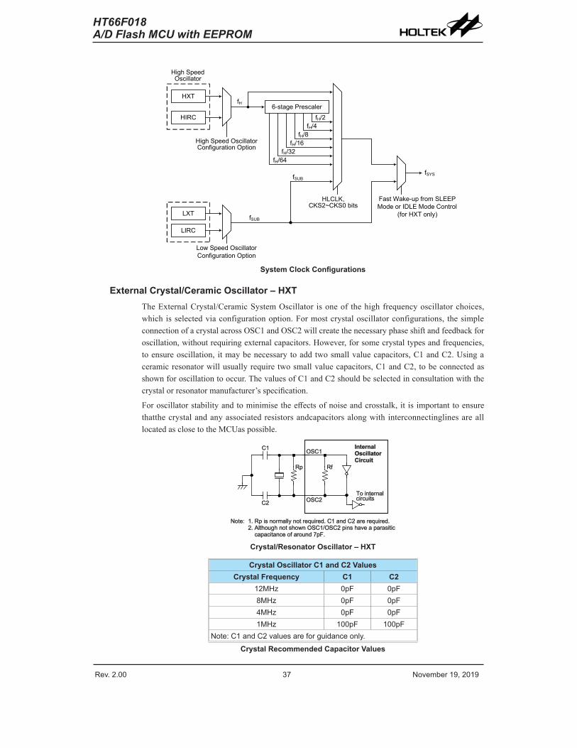
Rev. 2.00 36 November 19, 2019 Rev. 2.00 37 November 19, 2019
HT66F018A/D Flash MCU with EEPROM
HT66F018A/D Flash MCU with EEPROM
HXT
HIRC
fH6-stage Prescaler
High Speed Oscillator Configuration Option
HLCLK, CKS2~CKS0 bits
fH/2fH/4
fH/8fH/16
fH/32fH/64
fSUB
Fast Wake-up from SLEEP Mode or IDLE Mode Control
(for HXT only)
fSYS
High Speed Oscillator
LIRC
LXT
Low Speed Oscillator Configuration Option
fSUB
System Clock Configurations
External Crystal/Ceramic Oscillator – HXT The External Crystal/Ceramic System Oscillator is one of the high frequency oscillator choices, which is selected via configuration option. For most crystal oscillator configurations, the simple connection of a crystal across OSC1 and OSC2 will create the necessary phase shift and feedback for oscillation, without requiring external capacitors. However, for some crystal types and frequencies, to ensure oscillation, it may be necessary to add two small value capacitors, C1 and C2. Using a ceramic resonator will usually require two small value capacitors, C1 and C2, to be connected as shown for oscillation to occur. The values of C1 and C2 should be selected in consultation with the crystal or resonator manufacturer’s specification.
For oscillator stability and to minimise the effects of noise and crosstalk, it is important to ensure thatthe crystal and any associated resistors andcapacitors along with interconnectinglines are all located as close to the MCUas possible.
Crystal/Resonator Oscillator – HXT
Crystal Oscillator C1 and C2 ValuesCrystal Frequency C1 C2
12MHz 0pF 0pF8MHz 0pF 0pF4MHz 0pF 0pF1MHz 100pF 100pF
Note: C1 and C2 values are for guidance only.Crystal Recommended Capacitor Values
Rev. 2.00 38 November 19, 2019 Rev. 2.00 39 November 19, 2019
HT66F018A/D Flash MCU with EEPROM
HT66F018A/D Flash MCU with EEPROM
Internal RC Oscillator – HIRC The internal RC oscillator is a fully integrated system oscillator requiring no external components. The internal RC oscillator has three fixed frequencies of 8MHz, 12MHz, 16MHz. Device trimming during the manufacturing process and the inclusion of internal frequency compensation circuits are used to ensure that the influence of the power supply voltage, temperature and process variations on the oscillation frequency are minimised. As a result, at a power supply of either 3V or 5V and at a temperature of 25°C degrees, the fixed oscillation frequency of 8MHz, 12MHz or 16MHz will have a tolerance within 2%. Note that if this internal system clock option is selected, as it requires no external pins for its operation, I/O pins are free for use as normal I/O pins.
External 32.768kHz Crystal Oscillator – LXTThe External 32.768kHz Crystal System Oscillator is one of the low frequency oscillator choices, which is selected via configuration option. This clock source has a fixed frequency of 32.768kHz and requires a 32.768kHz crystal to be connected between pins XT1 and XT2. The external resistor and capacitor components connected to the 32.768kHz crystal are necessary to provide oscillation. For applications where precise frequencies are essential, these components may be required to provide frequency compensation due to different crystal manufacturing tolerances. During power-up there is a time delay associated with the LXT oscillator waiting for it to start-up.
When the microcontroller enters the SLEEP or IDLE Mode, the system clock is switched off to stop microcontroller activity and to conserve power. However, in many microcontroller applications it may be necessary to keep the internal timers operational even when the microcontroller is in the SLEEP or IDLE Mode. To do this, another clock, independent of the system clock, must be provided.
However, for some crystals, to ensure oscillation and accurate frequency generation, it is necessary to add two small value external capacitors, C1 and C2. The exact values of C1 and C2 should be selected in consultation with the crystal or resonator manufacturer specification. The external parallel feedback resistor, RP, is required.
Some configuration options determine if the XT1/XT2 pins are used for the LXT oscillator or as I/O pins.
• If the LXT oscillator is not used for any clock source, the XT1/XT2 pins can be used as normal I/O or other pin-shared functional pins.
• If the LXT oscillator is used for any clock source, the 32.768kHz crystal should be connected to the XT1/XT2 pins.
For oscillator stability and to minimise the effects of noise and crosstalk, it is important to ensure thatthe crystal and any associated resistors andcapacitors along with interconnectinglines are all located as close to the MCUas possible.
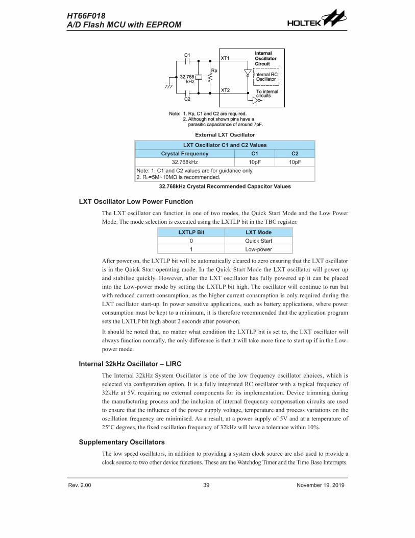
Rev. 2.00 38 November 19, 2019 Rev. 2.00 39 November 19, 2019
HT66F018A/D Flash MCU with EEPROM
HT66F018A/D Flash MCU with EEPROM
External LXT Oscillator
LXT Oscillator C1 and C2 ValuesCrystal Frequency C1 C2
32.768kHz 10pF 10pFNote: 1. C1 and C2 values are for guidance only.2. RP=5M~10MΩ is recommended.
32.768kHz Crystal Recommended Capacitor Values
LXT Oscillator Low Power Function The LXT oscillator can function in one of two modes, the Quick Start Mode and the Low Power Mode. The mode selection is executed using the LXTLP bit in the TBC register.
LXTLP Bit LXT Mode0 Quick Start1 Low-power
After power on, the LXTLP bit will be automatically cleared to zero ensuring that the LXT oscillator is in the Quick Start operating mode. In the Quick Start Mode the LXT oscillator will power up and stabilise quickly. However, after the LXT oscillator has fully powered up it can be placed into the Low-power mode by setting the LXTLP bit high. The oscillator will continue to run but with reduced current consumption, as the higher current consumption is only required during the LXT oscillator start-up. In power sensitive applications, such as battery applications, where power consumption must be kept to a minimum, it is therefore recommended that the application program sets the LXTLP bit high about 2 seconds after power-on.
It should be noted that, no matter what condition the LXTLP bit is set to, the LXT oscillator will always function normally, the only difference is that it will take more time to start up if in the Low-power mode.
Internal 32kHz Oscillator – LIRC The Internal 32kHz System Oscillator is one of the low frequency oscillator choices, which is selected via configuration option. It is a fully integrated RC oscillator with a typical frequency of 32kHz at 5V, requiring no external components for its implementation. Device trimming during the manufacturing process and the inclusion of internal frequency compensation circuits are used to ensure that the influence of the power supply voltage, temperature and process variations on the oscillation frequency are minimised. As a result, at a power supply of 5V and at a temperature of 25°C degrees, the fixed oscillation frequency of 32kHz will have a tolerance within 10%.
Supplementary Oscillators The low speed oscillators, in addition to providing a system clock source are also used to provide a clock source to two other device functions. These are the Watchdog Timer and the Time Base Interrupts.
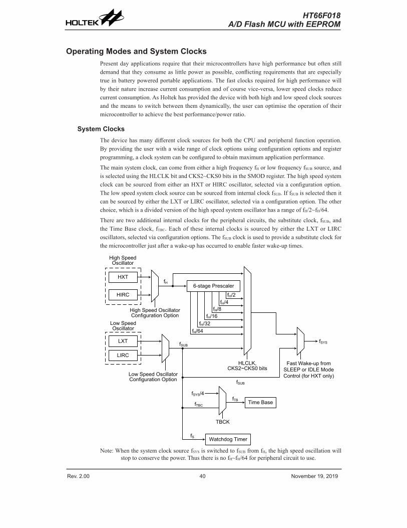
Rev. 2.00 40 November 19, 2019 Rev. 2.00 41 November 19, 2019
HT66F018A/D Flash MCU with EEPROM
HT66F018A/D Flash MCU with EEPROM
Operating Modes and System Clocks Present day applications require that their microcontrollers have high performance but often still demand that they consume as little power as possible, conflicting requirements that are especially true in battery powered portable applications. The fast clocks required for high performance will by their nature increase current consumption and of course vice-versa, lower speed clocks reduce current consumption. As Holtek has provided the device with both high and low speed clock sources and the means to switch between them dynamically, the user can optimise the operation of their microcontroller to achieve the best performance/power ratio.
System Clocks The device has many different clock sources for both the CPU and peripheral function operation. By providing the user with a wide range of clock options using configuration options and register programming, a clock system can be configured to obtain maximum application performance.
The main system clock, can come from either a high frequency fH or low frequency fSUB source, and is selected using the HLCLK bit and CKS2~CKS0 bits in the SMOD register. The high speed system clock can be sourced from either an HXT or HIRC oscillator, selected via a configuration option. The low speed system clock source can be sourced from internal clock fSUB. If fSUB is selected then it can be sourced by either the LXT or LIRC oscillator, selected via a configuration option. The other choice, which is a divided version of the high speed system oscillator has a range of fH/2~fH/64.
There are two additional internal clocks for the peripheral circuits, the substitute clock, fSUB, and the Time Base clock, fTBC. Each of these internal clocks is sourced by either the LXT or LIRC oscillators, selected via configuration options. The fSUB clock is used to provide a substitute clock for the microcontroller just after a wake-up has occurred to enable faster wake-up times.
HXT
HIRC
LIRC
Low Speed Oscillator
fH6-stage Prescaler
High Speed Oscillator Configuration Option
HLCLK, CKS2~CKS0 bits
fH/2fH/4
fH/8fH/16
fH/32fH/64
fSUB
Fast Wake-up from SLEEP or IDLE Mode Control (for HXT only)
fSYSLXT
High Speed Oscillator
Low Speed Oscillator Configuration Option
fSYS/4
Time BasefTB
TBCK
fTBC
Watchdog TimerfS
fSUB
Note: When the system clock source fSYS is switched to fSUB from fH, the high speed oscillation will stop to conserve the power. Thus there is no fH~fH/64 for peripheral circuit to use.
Rev. 2.00 40 November 19, 2019 Rev. 2.00 41 November 19, 2019
HT66F018A/D Flash MCU with EEPROM
HT66F018A/D Flash MCU with EEPROM
System Operation Modes There are six different modes of operation for the microcontroller, each one with its own special characteristics and which can be chosen according to the specific performance and power requirements of the application. There are two modes allowing normal operation of the microcontroller, the NORMAL Mode and SLOW Mode. The remaining four modes, the SLEEP0, SLEEP1, IDLE0 and IDLE1 Mode are used when the microcontroller CPU is switched off to conserve power.
Operating ModeDescription
CPU fSYS fSUB fS fTBC
NORMAL Mode on fH~fH/64 on on on
SLOW Mode on fSUB on on on
IDLE0 Mode off off on on on
IDLE1 Mode off on on on on
SLEEP0 Mode off off off off off
SLEEP1 Mode off off on on off
• NORMAL Mode As the name suggests this is one of the main operating modes where the microcontroller has all of its functions operational and where the system clock is provided by one of the high speed oscillators. This mode operates allowing the microcontroller to operate normally with a clock source will come from one of the high speed oscillators, either the HXT or HIRC oscillators. The high speed oscillator will however first be divided by a ratio ranging from 1 to 64, the actual ratio being selected by the CKS2~CKS0 and HLCLK bits in the SMOD register. Although a high speed oscillator is used, running the microcontroller at a divided clock ratio reduces the operating current.
• SLOW Mode This is also a mode where the microcontroller operates normally although now with a slower speed clock source. The clock source used will be from one of the low speed oscillators, either the LXT or the LIRC. Running the microcontroller in this mode allows it to run with much lower operating currents. In the SLOW Mode, the fH is off.
• SLEEP0 ModeThe SLEEP Mode is entered when an HALT instruction is executed and when the IDLEN bit in the SMOD register is low. In the SLEEP0 mode the CPU will be stopped, and the fSUB and fS clocks will be stopped too, and the Watchdog Timer function is disabled. In this mode, the LVDEN is must set to “0”. If the LVDEN is set to “1”, it won’t enter the SLEEP0 Mode.
• SLEEP1 ModeThe SLEEP Mode is entered when an HALT instruction is executed and when the IDLEN bit in the SMOD register is low. In the SLEEP1 mode the CPU will be stopped. However the fSUB and fS clocks will continue to operate if the LVDEN is “1” or the Watchdog Timer function is enabled and if its clock source is chosen via configuration option to come from the fSUB.
• IDLE0 Mode The IDLE0 Mode is entered when a HALT instruction is executed and when the IDLEN bit in the SMOD register is high and the FSYSON bit in the CTRL register is low. In the IDLE0 Mode the system oscillator will be inhibited from driving the CPU but some peripheral functions will remain operational such as the Watchdog Timer and TMs. In the IDLE0 Mode, the system oscillator will be stopped.
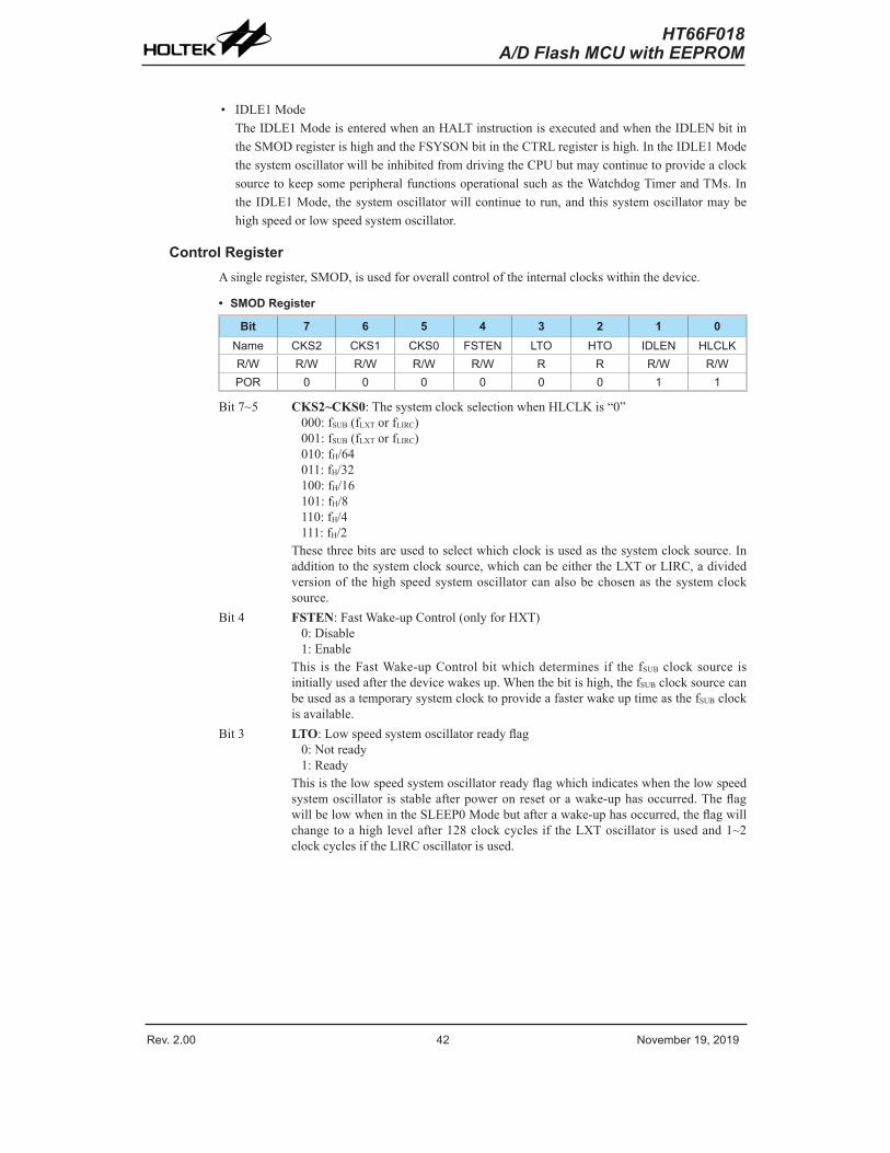
Rev. 2.00 42 November 19, 2019 Rev. 2.00 43 November 19, 2019
HT66F018A/D Flash MCU with EEPROM
HT66F018A/D Flash MCU with EEPROM
• IDLE1 Mode The IDLE1 Mode is entered when an HALT instruction is executed and when the IDLEN bit in the SMOD register is high and the FSYSON bit in the CTRL register is high. In the IDLE1 Mode the system oscillator will be inhibited from driving the CPU but may continue to provide a clock source to keep some peripheral functions operational such as the Watchdog Timer and TMs. In the IDLE1 Mode, the system oscillator will continue to run, and this system oscillator may be high speed or low speed system oscillator.
Control RegisterA single register, SMOD, is used for overall control of the internal clocks within the device.
• SMOD Register
Bit 7 6 5 4 3 2 1 0Name CKS2 CKS1 CKS0 FSTEN LTO HTO IDLEN HLCLKR/W R/W R/W R/W R/W R R R/W R/WPOR 0 0 0 0 0 0 1 1
Bit 7~5 CKS2~CKS0: The system clock selection when HLCLK is “0”000: fSUB (fLXT or fLIRC)001: fSUB (fLXT or fLIRC)010: fH/64011: fH/32100: fH/16101: fH/8110: fH/4111: fH/2
These three bits are used to select which clock is used as the system clock source. In addition to the system clock source, which can be either the LXT or LIRC, a divided version of the high speed system oscillator can also be chosen as the system clock source.
Bit 4 FSTEN: Fast Wake-up Control (only for HXT)0: Disable1: Enable
This is the Fast Wake-up Control bit which determines if the fSUB clock source is initially used after the device wakes up. When the bit is high, the fSUB clock source can be used as a temporary system clock to provide a faster wake up time as the fSUB clock is available.
Bit 3 LTO: Low speed system oscillator ready flag0: Not ready1: Ready
This is the low speed system oscillator ready flag which indicates when the low speed system oscillator is stable after power on reset or a wake-up has occurred. The flag will be low when in the SLEEP0 Mode but after a wake-up has occurred, the flag will change to a high level after 128 clock cycles if the LXT oscillator is used and 1~2 clock cycles if the LIRC oscillator is used.
Rev. 2.00 42 November 19, 2019 Rev. 2.00 43 November 19, 2019
HT66F018A/D Flash MCU with EEPROM
HT66F018A/D Flash MCU with EEPROM
Bit 2 HTO: High speed system oscillator ready flag0: Not ready1: Ready
This is the high speed system oscillator ready flag which indicates when the high speed system oscillator is stable. This flag is cleared to “0” by hardware when the device is powered on and then changes to a high level after the high speed system oscillator is stable. Therefore this flag will always be read as “1” by the application program after device power-on. The flag will be low when in the SLEEP or IDLE0 Mode but after a wake-up has occurred, the flag will change to a high level after 512 clock cycles if the HXT oscillator is used and after 15~16 clock cycles if the HIRC oscillator is used.
Bit 1 IDLEN: IDLE Mode control0: Disable1: Enable
This is the IDLE Mode Control bit and determines what happens when the HALT instruction is executed. If this bit is high, when a HALT instruction is executed the device will enter the IDLE Mode. In the IDLE1 Mode the CPU will stop running but the system clock will continue to keep the peripheral functions operational, if FSYSON bit is high. If FSYSON bit is low, the CPU and the system clock will all stop in IDLE0 mode. If the bit is low the device will enter the SLEEP Mode when a HALT instruction is executed.
Bit 0 HLCLK: system clock selection0: fH/2~fH/64 or fSUB
1: fH
This bit is used to select if the fH clock or the fH/2~fH/64 or fSUB clock is used as the system clock. When the bit is high the fH clock will be selected and if low the fH/2~fH/64 or fSUB clock will be selected. When system clock switches from the fH clock to the fSUB clock and the fH clock will be automatically switched off to conserve power.
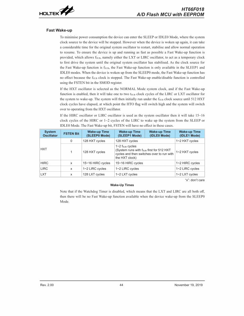
Rev. 2.00 44 November 19, 2019 Rev. 2.00 45 November 19, 2019
HT66F018A/D Flash MCU with EEPROM
HT66F018A/D Flash MCU with EEPROM
Fast Wake-up To minimise power consumption the device can enter the SLEEP or IDLE0 Mode, where the system clock source to the device will be stopped. However when the device is woken up again, it can take a considerable time for the original system oscillator to restart, stabilise and allow normal operation to resume. To ensure the device is up and running as fast as possible a Fast Wake-up function is provided, which allows fSUB, namely either the LXT or LIRC oscillator, to act as a temporary clock to first drive the system until the original system oscillator has stabilised. As the clock source for the Fast Wake-up function is fSUB, the Fast Wake-up function is only available in the SLEEP1 and IDLE0 modes. When the device is woken up from the SLEEP0 mode, the Fast Wake-up function has no effect because the fSUB clock is stopped. The Fast Wake-up enable/disable function is controlled using the FSTEN bit in the SMOD register.
If the HXT oscillator is selected as the NORMAL Mode system clock, and if the Fast Wake-up function is enabled, then it will take one to two tSUB clock cycles of the LIRC or LXT oscillator for the system to wake-up. The system will then initially run under the fSUB clock source until 512 HXT clock cycles have elapsed, at which point the HTO flag will switch high and the system will switch over to operating from the HXT oscillator.
If the HIRC oscillator or LIRC oscillator is used as the system oscillator then it will take 15~16 clock cycles of the HIRC or 1~2 cycles of the LIRC to wake up the system from the SLEEP or IDLE0 Mode. The Fast Wake-up bit, FSTEN will have no effect in these cases.
System Oscillator FSTEN Bit Wake-up Time
(SLEEP0 Mode)Wake-up Time
(SLEEP1 Mode)Wake-up Time(IDLE0 Mode)
Wake-up Time(IDLE1 Mode)
HXT
0 128 HXT cycles 128 HXT cycles 1~2 HXT cycles
1 128 HXT cycles
1~2 fSUB cycles(System runs with fSUB first for 512 HXT cycles and then switches over to run with the HXT clock)
1~2 HXT cycles
HIRC x 15~16 HIRC cycles 15~16 HIRC cycles 1~2 HIRC cycles
LIRC x 1~2 LIRC cycles 1~2 LIRC cycles 1~2 LIRC cycles
LXT x 128 LXT cycles 1~2 LXT cycles 1~2 LXT cycles
“x”: don’t careWake-Up Times
Note that if the Watchdog Timer is disabled, which means that the LXT and LIRC are all both off, then there will be no Fast Wake-up function available when the device wake-up from the SLEEP0 Mode.

Rev. 2.00 44 November 19, 2019 Rev. 2.00 45 November 19, 2019
HT66F018A/D Flash MCU with EEPROM
HT66F018A/D Flash MCU with EEPROM
Operating Mode Switching The device can switch between operating modes dynamically allowing the user to select the best performance/power ratio for the present task in hand. In this way microcontroller operations that do not require high performance can be executed using slower clocks thus requiring less operating current and prolonging battery life in portable applications.
In simple terms, Mode Switching between the NORMAL Mode and SLOW Mode is executed using the HLCLK bit and CKS2~CKS0 bits in the SMOD register while Mode Switching from the NORMAL/SLOW Modes to the SLEEP/IDLE Modes is executed via the HALT instruction. When a HALT instruction is executed, whether the device enters the IDLE Mode or the SLEEP Mode is determined by the condition of the IDLEN bit in the SMOD register and FSYSON in the CTRL register.
When the HLCLK bit switches to a low level, which implies that clock source is switched from the high speed clock source, fH, to the clock source, fH/2~fH/64 or fSUB. If the clock is from the fSUB, the high speed clock source will stop running to conserve power. When this happens it must be noted that the fH/16 and fH/64 internal clock sources will also stop running, which may affect the operation of other internal functions such as the TMs. The accompanying flowchart shows what happens when the device moves between the various operating modes.

Rev. 2.00 46 November 19, 2019 Rev. 2.00 47 November 19, 2019
HT66F018A/D Flash MCU with EEPROM
HT66F018A/D Flash MCU with EEPROM
NORMAL Mode to SLOW Mode Switching When running in the NORMAL Mode, which uses the high speed system oscillator, and therefore consumes more power, the system clock can switch to run in the SLOW Mode by set the HLCLK bit to “0” and set the CKS2~CKS0 bits to “000” or “001” in the SMOD register. This will then use the low speed system oscillator which will consume less power. Users may decide to do this for certain operations which do not require high performance and can subsequently reduce power consumption.
The SLOW Mode is sourced from the LXT or the LIRC oscillators and therefore requires these oscillators to be stable before full mode switching occurs. This is monitored using the LTO bit in the SMOD register.
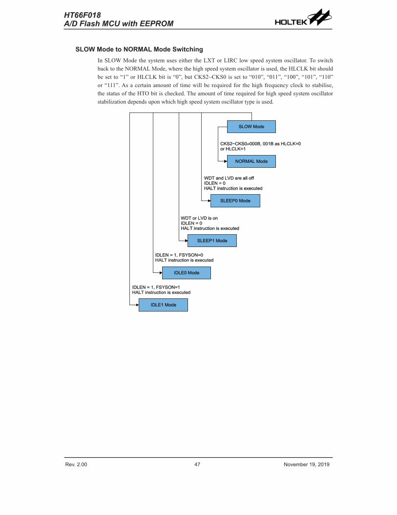
Rev. 2.00 46 November 19, 2019 Rev. 2.00 47 November 19, 2019
HT66F018A/D Flash MCU with EEPROM
HT66F018A/D Flash MCU with EEPROM
SLOW Mode to NORMAL Mode Switching In SLOW Mode the system uses either the LXT or LIRC low speed system oscillator. To switch back to the NORMAL Mode, where the high speed system oscillator is used, the HLCLK bit should be set to “1” or HLCLK bit is “0”, but CKS2~CKS0 is set to “010”, “011”, “100”, “101”, “110” or “111”. As a certain amount of time will be required for the high frequency clock to stabilise, the status of the HTO bit is checked. The amount of time required for high speed system oscillator stabilization depends upon which high speed system oscillator type is used.
Rev. 2.00 48 November 19, 2019 Rev. 2.00 49 November 19, 2019
HT66F018A/D Flash MCU with EEPROM
HT66F018A/D Flash MCU with EEPROM
Entering the SLEEP0 Mode There is only one way for the device to enter the SLEEP0 Mode and that is to execute the “HALT” instruction in the application program with the IDLEN bit in SMOD register equal to “0” and the WDT and LVD both off. When this instruction is executed under the conditions described above, the following will occur:
• The system clock, WDT clock and Time Base clock will be stopped and the application program will stop at the “HALT” instruction.
• The Data Memory contents and registers will maintain their present condition.
• The WDT will be cleared and stopped no matter if the WDT clock source originates from the fSUB clock or from the system clock.
• The I/O ports will maintain their present conditions.
• In the status register, the Power Down flag, PDF, will be set and the Watchdog time-out flag, TO, will be cleared.
Entering the SLEEP1 Mode There is only one way for the device to enter the SLEEP1 Mode and that is to execute the “HALT” instruction in the application program with the IDLEN bit in SMOD register equal to “0” and the WDT or LVD on. When this instruction is executed under the conditions described above, the following will occur:
• The system clock and Time Base clock will be stopped and the application program will stop at the “HALT” instruction, but the WDT or LVD will remain with the clock source coming from the fSUB clock.
• The Data Memory contents and registers will maintain their present condition.
• The WDT will be cleared and resume counting if the WDT is enabled.
• The I/O ports will maintain their present conditions.
• In the status register, the Power Down flag, PDF, will be set and the Watchdog time-out flag, TO, will be cleared.
Entering the IDLE0 Mode There is only one way for the device to enter the IDLE0 Mode and that is to execute the “HALT” instruction in the application program with the IDLEN bit in SMOD register equal to “1” and the FSYSON bit in CTRL register equal to “0”. When this instruction is executed under the conditions described above, the following will occur:
• The system clock will be stopped and the application program will stop at the “HALT” instruction, but the Time Base clock and fSUB clock will be on.
• The Data Memory contents and registers will maintain their present condition.
• The WDT will be cleared and resume counting if the WDT is enabled.
• The I/O ports will maintain their present conditions.
• In the status register, the Power Down flag, PDF, will be set and the Watchdog time-out flag, TO, will be cleared.
Rev. 2.00 48 November 19, 2019 Rev. 2.00 49 November 19, 2019
HT66F018A/D Flash MCU with EEPROM
HT66F018A/D Flash MCU with EEPROM
Entering the IDLE1 Mode There is only one way for the device to enter the IDLE1 Mode and that is to execute the “HALT” instruction in the application program with the IDLEN bit in SMOD register equal to “1” and the FSYSON bit in CTRL register equal to “1”. When this instruction is executed under the conditions described above, the following will occur:
• The system clock and Time Base clock and fSUB clock will be on and the application program will stop at the “HALT” instruction.
• The Data Memory contents and registers will maintain their present condition.
• The WDT will be cleared and resume counting if the WDT is enabled.
• The I/O ports will maintain their present conditions.
• In the status register, the Power Down flag, PDF, will be set and the Watchdog time-out flag, TO, will be cleared.
Standby Current Considerations As the main reason for entering the SLEEP or IDLE Mode is to keep the current consumption of the device to as low a value as possible, perhaps only in the order of several micro-amps except in the IDLE1 Mode, there are other considerations which must also be taken into account by the circuit designer if the power consumption is to be minimised. Special attention must be made to the I/O pins on the device. All high-impedance input pins must be connected to either a fixed high or low level as any floating input pins could create internal oscillations and result in increased current consumption. This also applies to the device which has different package types, as there may be unbonbed pins. These must either be setup as outputs or if setup as inputs must have pull-high resistors connected.
Care must also be taken with the loads, which are connected to I/O pins, which are setup as outputs. These should be placed in a condition in which minimum current is drawn or connected only to external circuits that do not draw current, such as other CMOS inputs. Also note that additional standby current will also be required if the configuration options have enabled the LXT or LIRC oscillator.
In the IDLE1 Mode the system oscillator is on, if the system oscillator is from the high speed system oscillator, the additional standby current will also be perhaps in the order of several hundred micro-amps.
Rev. 2.00 50 November 19, 2019 Rev. 2.00 51 November 19, 2019
HT66F018A/D Flash MCU with EEPROM
HT66F018A/D Flash MCU with EEPROM
Wake-up After the system enters the SLEEP or IDLE Mode, it can be woken up from one of various sources listed as follows:
• An external falling edge on Port A
• A system interrupt
• A WDT overflow
If the device is woken up by a WDT overflow, a Watchdog Timer reset will be initiated. Although both of these wake-up methods will initiate a reset operation, the actual source of the wake-up can be determined by examining the TO and PDF flags. The PDF flag is cleared by a system power-up or executing the clear Watchdog Timer instructions and is set when executing the “HALT” instruction. The TO flag is set if a WDT time-out occurs, and causes a wake-up that only resets the Program Counter and Stack Pointer, the other flags remain in their original status.
Each pin on Port A can be setup using the PAWU register to permit a negative transition on the pin to wake-up the system. When a Port A pin wake-up occurs, the program will resume execution at the instruction following the “HALT” instruction. If the system is woken up by an interrupt, then two possible situations may occur. The first is where the related interrupt is disabled or the interrupt is enabled but the stack is full, in which case the program will resume execution at the instruction following the “HALT” instruction. In this situation, the interrupt which woke-up the device will not be immediately serviced, but will rather be serviced later when the related interrupt is finally enabled or when a stack level becomes free. The other situation is where the related interrupt is enabled and the stack is not full, in which case the regular interrupt response takes place. If an interrupt request flag is set high before entering the SLEEP or IDLE Mode, the wake-up function of the related interrupt will be disabled.
Programming Considerations The high speed and low speed oscillators both use the same SST counter. For example, if the system is woken up from the SLEEP0 Mode and both the HIRC and LXT oscillators need to start-up from an off state. The LXT oscillator uses the SST counter after HIRC oscillator has finished its SST period.
• If the device is woken up from the SLEEP0 Mode to the NORMAL Mode, the high speed system oscillator needs an SST period. The device will execute first instruction after HTO is “1”. At this time, the LXT oscillator may not be stability if fSUB is from LXT oscillator. The same situation occurs in the power-on state. The LXT oscillator is not ready yet when the first instruction is executed.
• If the device is woken up from the SLEEP1 Mode to NORMAL Mode, and the system clock source is from HXT oscillator and FSTEN is “1”, the system clock can be switched to the LIRC oscillator after wake up.
• There are peripheral functions, such as WDT and TMs, for which the fSYS is used. If the system clock source is switched from fH to fSUB, the clock source to the peripheral functions mentioned above will change accordingly.
• The on/off condition of fSUB and fS depends upon whether the WDT is enabled or disabled as the WDT clock source is selected from fSUB.
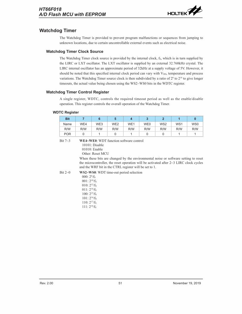
Rev. 2.00 50 November 19, 2019 Rev. 2.00 51 November 19, 2019
HT66F018A/D Flash MCU with EEPROM
HT66F018A/D Flash MCU with EEPROM
Watchdog TimerThe Watchdog Timer is provided to prevent program malfunctions or sequences from jumping to unknown locations, due to certain uncontrollable external events such as electrical noise.
Watchdog Timer Clock SourceThe Watchdog Timer clock source is provided by the internal clock, fS, which is in turn supplied by the LIRC or LXT oscillator. The LXT oscillator is supplied by an external 32.768kHz crystal. The LIRC internal oscillator has an approximate period of 32kHz at a supply voltage of 5V. However, it should be noted that this specified internal clock period can vary with VDD, temperature and process variations. The Watchdog Timer source clock is then subdivided by a ratio of 28 to 218 to give longer timeouts, the actual value being chosen using the WS2~WS0 bits in the WDTC register.
Watchdog Timer Control RegisterA single register, WDTC, controls the required timeout period as well as the enable/disable operation. This register controls the overall operation of the Watchdog Timer.
WDTC RegisterBit 7 6 5 4 3 2 1 0
Name WE4 WE3 WE2 WE1 WE0 WS2 WS1 WS0R/W R/W R/W R/W R/W R/W R/W R/W R/WPOR 0 1 0 1 0 0 1 1
Bit 7~3 WE4~WE0: WDT function software control10101: Disable01010: EnableOther: Reset MCU
When these bits are changed by the environmental noise or software setting to reset the microcontroller, the reset operation will be activated after 2~3 LIRC clock cycles and the WRF bit in the CTRL register will be set to 1.
Bit 2~0 WS2~WS0: WDT time-out period selection000: 28/fS
001: 210/fS
010: 212/fS
011: 214/fS
100: 215/fS
101: 216/fS
110: 217/fS
111: 218/fS
Rev. 2.00 52 November 19, 2019 Rev. 2.00 53 November 19, 2019
HT66F018A/D Flash MCU with EEPROM
HT66F018A/D Flash MCU with EEPROM
CTRL RegisterBit 7 6 5 4 3 2 1 0
Name FSYSON — — — — LVRF LRF WRFR/W R/W — — — — R/W R/W R/WPOR 0 — — — — x 0 0
“x” unknownBit 7 FSYSON: fSYS Control in IDLE Mode
Described elsewhere Bit 6~3 Unimplemented, read as “0”Bit 2 LVRF: LVR function reset flag
Described elsewhere Bit 1 LRF: LVR Control register software reset flag
Described elsewhere Bit 0 WRF: WDT Control register software reset flag
0: Not occur1: Occurred
This bit is set to 1 by the WDT Control register software reset and cleared by the application program. Note that this bit can only be cleared to 0 by the application program.
Watchdog Timer OperationThe Watchdog Timer operates by providing a device reset when its timer overflows. This means that in the application program and during normal operation the user has to strategically clear the Watchdog Timer before it overflows to prevent the Watchdog Timer from executing a reset. This is done using the clear watchdog instructions. If the program malfunctions for whatever reason, jumps to an unknown location, or enters an endless loop, these clear instructions will not be executed in the correct manner, in which case the Watchdog Timer will overflow and reset the device. With regard to the Watchdog Timer enable/disable function, there are five bits, WE4~WE0, in the WDTC register to offer additional enable/disable and reset control of the Watchdog Timer. The WDT function will be disabled when the WE4~WE0 bits are set to a value of 10101B. The WDT function will be enabled if the WE4~WE0 bits value is equal to 01010B. If the WE4~WE0 bits are set to any other values by the environmental noise or software setting, except 01010B and 10101B, it will reset the device after 2~3 LIRC clock cycles. After power on these bits will have the value of 01010B.
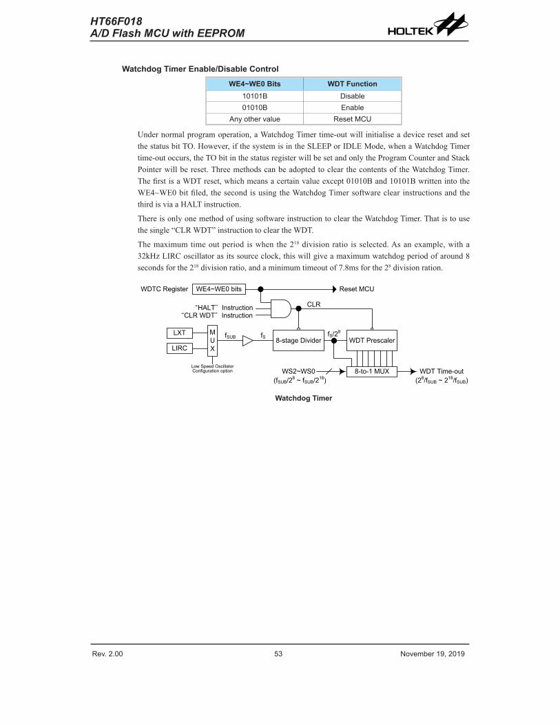
Rev. 2.00 52 November 19, 2019 Rev. 2.00 53 November 19, 2019
HT66F018A/D Flash MCU with EEPROM
HT66F018A/D Flash MCU with EEPROM
Watchdog Timer Enable/Disable ControlWE4~WE0 Bits WDT Function
10101B Disable01010B Enable
Any other value Reset MCU
Under normal program operation, a Watchdog Timer time-out will initialise a device reset and set the status bit TO. However, if the system is in the SLEEP or IDLE Mode, when a Watchdog Timer time-out occurs, the TO bit in the status register will be set and only the Program Counter and Stack Pointer will be reset. Three methods can be adopted to clear the contents of the Watchdog Timer. The first is a WDT reset, which means a certain value except 01010B and 10101B written into the WE4~WE0 bit filed, the second is using the Watchdog Timer software clear instructions and the third is via a HALT instruction.
There is only one method of using software instruction to clear the Watchdog Timer. That is to use the single “CLR WDT” instruction to clear the WDT.
The maximum time out period is when the 218 division ratio is selected. As an example, with a 32kHz LIRC oscillator as its source clock, this will give a maximum watchdog period of around 8 seconds for the 218 division ratio, and a minimum timeout of 7.8ms for the 28 division ration.
“CLR WDT”Instruction
8-stage Divider WDT Prescaler
WE4~WE0 bitsWDTC Register Reset MCU
LXT fSUB fS/28
8-to-1 MUX
CLR
WS2~WS0(fSUB/28 ~ fSUB/218)
WDT Time-out(28/fSUB ~ 218/fSUB)
LIRC
MUX
Low Speed Oscillator Configuration option
“HALT”Instruction
fS
Watchdog Timer
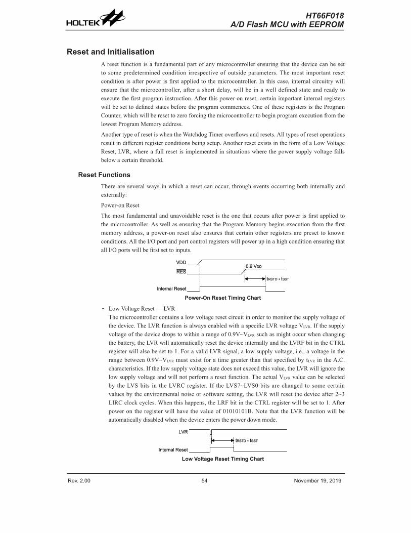
Rev. 2.00 54 November 19, 2019 Rev. 2.00 55 November 19, 2019
HT66F018A/D Flash MCU with EEPROM
HT66F018A/D Flash MCU with EEPROM
Reset and InitialisationA reset function is a fundamental part of any microcontroller ensuring that the device can be set to some predetermined condition irrespective of outside parameters. The most important reset condition is after power is first applied to the microcontroller. In this case, internal circuitry will ensure that the microcontroller, after a short delay, will be in a well defined state and ready to execute the first program instruction. After this power-on reset, certain important internal registers will be set to defined states before the program commences. One of these registers is the Program Counter, which will be reset to zero forcing the microcontroller to begin program execution from the lowest Program Memory address.
Another type of reset is when the Watchdog Timer overflows and resets. All types of reset operations result in different register conditions being setup. Another reset exists in the form of a Low Voltage Reset, LVR, where a full reset is implemented in situations where the power supply voltage falls below a certain threshold.
Reset Functions There are several ways in which a reset can occur, through events occurring both internally and externally:
Power-on Reset
The most fundamental and unavoidable reset is the one that occurs after power is first applied to the microcontroller. As well as ensuring that the Program Memory begins execution from the first memory address, a power-on reset also ensures that certain other registers are preset to known conditions. All the I/O port and port control registers will power up in a high condition ensuring that all I/O ports will be first set to inputs.
Power-On Reset Timing Chart
• Low Voltage Reset — LVR The microcontroller contains a low voltage reset circuit in order to monitor the supply voltage of the device. The LVR function is always enabled with a specific LVR voltage VLVR. If the supply voltage of the device drops to within a range of 0.9V~VLVR such as might occur when changing the battery, the LVR will automatically reset the device internally and the LVRF bit in the CTRL register will also be set to 1. For a valid LVR signal, a low supply voltage, i.e., a voltage in the range between 0.9V~VLVR must exist for a time greater than that specified by tLVR in the A.C. characteristics. If the low supply voltage state does not exceed this value, the LVR will ignore the low supply voltage and will not perform a reset function. The actual VLVR value can be selected by the LVS bits in the LVRC register. If the LVS7~LVS0 bits are changed to some certain values by the environmental noise or software setting, the LVR will reset the device after 2~3 LIRC clock cycles. When this happens, the LRF bit in the CTRL register will be set to 1. After power on the register will have the value of 01010101B. Note that the LVR function will be automatically disabled when the device enters the power down mode.
Low Voltage Reset Timing Chart
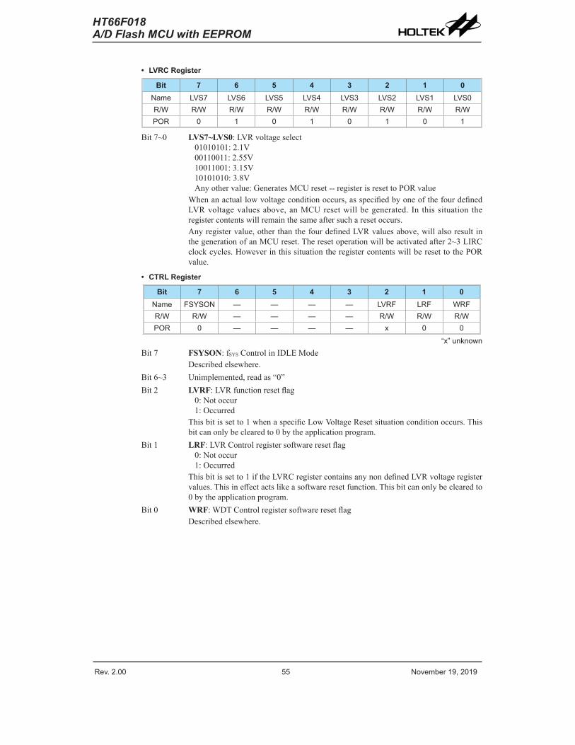
Rev. 2.00 54 November 19, 2019 Rev. 2.00 55 November 19, 2019
HT66F018A/D Flash MCU with EEPROM
HT66F018A/D Flash MCU with EEPROM
• LVRC Register
Bit 7 6 5 4 3 2 1 0Name LVS7 LVS6 LVS5 LVS4 LVS3 LVS2 LVS1 LVS0R/W R/W R/W R/W R/W R/W R/W R/W R/WPOR 0 1 0 1 0 1 0 1
Bit 7~0 LVS7~LVS0: LVR voltage select01010101: 2.1V00110011: 2.55V10011001: 3.15V10101010: 3.8VAny other value: Generates MCU reset -- register is reset to POR value
When an actual low voltage condition occurs, as specified by one of the four defined LVR voltage values above, an MCU reset will be generated. In this situation the register contents will remain the same after such a reset occurs.Any register value, other than the four defined LVR values above, will also result in the generation of an MCU reset. The reset operation will be activated after 2~3 LIRC clock cycles. However in this situation the register contents will be reset to the POR value.
• CTRL Register
Bit 7 6 5 4 3 2 1 0Name FSYSON — — — — LVRF LRF WRFR/W R/W — — — — R/W R/W R/WPOR 0 — — — — x 0 0
“x” unknownBit 7 FSYSON: fSYS Control in IDLE Mode
Described elsewhere.Bit 6~3 Unimplemented, read as “0”Bit 2 LVRF: LVR function reset flag
0: Not occur1: Occurred
This bit is set to 1 when a specific Low Voltage Reset situation condition occurs. This bit can only be cleared to 0 by the application program.
Bit 1 LRF: LVR Control register software reset flag0: Not occur1: Occurred
This bit is set to 1 if the LVRC register contains any non defined LVR voltage register values. This in effect acts like a software reset function. This bit can only be cleared to 0 by the application program.
Bit 0 WRF: WDT Control register software reset flagDescribed elsewhere.
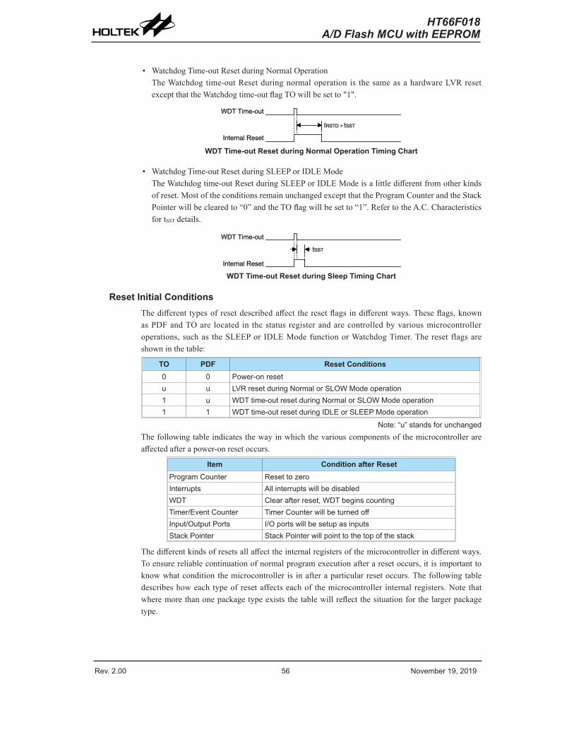
Rev. 2.00 56 November 19, 2019 Rev. 2.00 57 November 19, 2019
HT66F018A/D Flash MCU with EEPROM
HT66F018A/D Flash MCU with EEPROM
• Watchdog Time-out Reset during Normal Operation The Watchdog time-out Reset during normal operation is the same as a hardware LVR reset except that the Watchdog time-out flag TO will be set to "1".
WDT Time-out Reset during Normal Operation Timing Chart
• Watchdog Time-out Reset during SLEEP or IDLE Mode The Watchdog time-out Reset during SLEEP or IDLE Mode is a little different from other kinds of reset. Most of the conditions remain unchanged except that the Program Counter and the Stack Pointer will be cleared to “0” and the TO flag will be set to “1”. Refer to the A.C. Characteristics for tSST details.
WDT Time-out Reset during Sleep Timing Chart
Reset Initial Conditions The different types of reset described affect the reset flags in different ways. These flags, known as PDF and TO are located in the status register and are controlled by various microcontroller operations, such as the SLEEP or IDLE Mode function or Watchdog Timer. The reset flags are shown in the table:
TO PDF Reset Conditions0 0 Power-on resetu u LVR reset during Normal or SLOW Mode operation1 u WDT time-out reset during Normal or SLOW Mode operation1 1 WDT time-out reset during IDLE or SLEEP Mode operation
Note: “u” stands for unchangedThe following table indicates the way in which the various components of the microcontroller are affected after a power-on reset occurs.
Item Condition after ResetProgram Counter Reset to zeroInterrupts All interrupts will be disabledWDT Clear after reset, WDT begins countingTimer/Event Counter Timer Counter will be turned offInput/Output Ports I/O ports will be setup as inputsStack Pointer Stack Pointer will point to the top of the stack
The different kinds of resets all affect the internal registers of the microcontroller in different ways. To ensure reliable continuation of normal program execution after a reset occurs, it is important to know what condition the microcontroller is in after a particular reset occurs. The following table describes how each type of reset affects each of the microcontroller internal registers. Note that where more than one package type exists the table will reflect the situation for the larger package type.
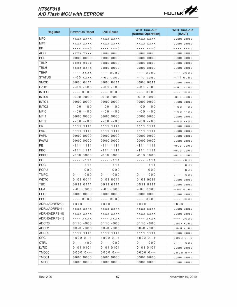
Rev. 2.00 56 November 19, 2019 Rev. 2.00 57 November 19, 2019
HT66F018A/D Flash MCU with EEPROM
HT66F018A/D Flash MCU with EEPROM
Register Power On Reset LVR Reset WDT Time-out(Normal Operation)
WDT Time-out(HALT)
MP0 x x x x x x x x x x x x x x x x x x x x x x x x u u u u u u u uMP1 x x x x x x x x x x x x x x x x x x x x x x x x u u u u u u u uBP - - - - - - - 0 - - - - - - - 0 - - - - - - - 0 - - - - - - - uACC x x x x x x x x u u u u u u u u u u u u u u u u u u u u u u u uPCL 0 0 0 0 0 0 0 0 0 0 0 0 0 0 0 0 0 0 0 0 0 0 0 0 0 0 0 0 0 0 0 0TBLP x x x x x x x x u u u u u u u u u u u u u u u u u u u u u u u uTBLH x x x x x x x x u u u u u u u u u u u u u u u u u u u u u u u uTBHP - - - - x x x x - - - - u u u u - - - - u u u u - - - - u u u uSTATUS - - 0 0 x x x x - - u u u u u u - - 1 u u u u u - - 1 1 u u u uSMOD 0 0 0 0 0 0 11 0 0 0 0 0 0 11 0 0 0 0 0 0 11 u u u u u u u uLVDC - - 0 0 - 0 0 0 - - 0 0 - 0 0 0 - - 0 0 - 0 0 0 - - u u - u u uINTEG - - - - 0 0 0 0 - - - - 0 0 0 0 - - - - 0 0 0 0 - - - - u u u uINTC0 - 0 0 0 0 0 0 0 - 0 0 0 0 0 0 0 - 0 0 0 0 0 0 0 - u u u u u u uINTC1 0 0 0 0 0 0 0 0 0 0 0 0 0 0 0 0 0 0 0 0 0 0 0 0 u u u u u u u uINTC2 - - 0 0 - - 0 0 - - 0 0 - - 0 0 - - 0 0 - - 0 0 - - u u - - u uMFI0 - - 0 0 - - 0 0 - - 0 0 - - 0 0 - - 0 0 - - 0 0 - - u u - - u uMFI1 0 0 0 0 0 0 0 0 0 0 0 0 0 0 0 0 0 0 0 0 0 0 0 0 u u u u u u u uMFI2 - - 0 0 - - 0 0 - - 0 0 - - 0 0 - - 0 0 - - 0 0 - - u u - - u uPA 1 1 1 1 1 1 1 1 1 1 1 1 1 1 1 1 1 1 1 1 1 1 1 1 u u u u u u u uPAC 1 1 1 1 1 1 1 1 1 1 1 1 1 1 1 1 1 1 1 1 1 1 1 1 u u u u u u u uPAPU 0 0 0 0 0 0 0 0 0 0 0 0 0 0 0 0 0 0 0 0 0 0 0 0 u u u u u u u uPAWU 0 0 0 0 0 0 0 0 0 0 0 0 0 0 0 0 0 0 0 0 0 0 0 0 u u u u u u u uPB - 1 1 1 1 1 1 1 - 1 1 1 1 1 1 1 - 1 1 1 1 1 1 1 - u u u u u u uPBC - 1 1 1 1 1 1 1 - 1 1 1 1 1 1 1 - 1 1 1 1 1 1 1 - u u u u u u uPBPU - 0 0 0 0 0 0 0 - 0 0 0 0 0 0 0 - 0 0 0 0 0 0 0 - u u u u u u uPC - - - - - 1 1 1 - - - - - 1 1 1 - - - - - 1 1 1 - - - - - u u uPCC - - - - - 1 1 1 - - - - - 1 1 1 - - - - - 1 1 1 - - - - - u u uPCPU - - - - - 0 0 0 - - - - - 0 0 0 - - - - - 0 0 0 - - - - - u u uTMPC 0 - - - - 0 0 0 0 - - - - 0 0 0 0 - - - - 0 0 0 u - - - - u u uWDTC 0 1 0 1 0 0 11 0 1 0 1 0 0 11 0 1 0 1 0 0 11 u u u u u u u uTBC 0 0 11 0 111 0 0 11 0 111 0 0 11 0 111 u u u u u u u uEEA - - 0 0 0 0 0 0 - - 0 0 0 0 0 0 - - 0 0 0 0 0 0 - - u u u u u uEED 0 0 0 0 0 0 0 0 0 0 0 0 0 0 0 0 0 0 0 0 0 0 0 0 u u u u u u u uEEC - - - - 0 0 0 0 - - - - 0 0 0 0 - - - - 0 0 0 0 - - - - u u u uADRL(ADRFS=0) x x x x - - - - x x x x - - - - x x x x - - - - u u u u - - - -ADRL(ADRFS=1) x x x x x x x x x x x x x x x x x x x x x x x x u u u u u u u uADRH(ADRFS=0) x x x x x x x x x x x x x x x x x x x x x x x x u u u u u u u uADRH(ADRFS=1) - - - - x x x x - - - - x x x x - - - - x x x x - - - - u u u uADCR0 0 11 0 - 0 0 0 0 11 0 - 0 0 0 0 11 0 - 0 0 0 u u u - - u u uADCR1 0 0 - 0 - 0 0 0 0 0 - 0 - 0 0 0 0 0 - 0 - 0 0 0 u u - u - u u uACERL 1 1 1 1 1 1 1 1 1 1 1 1 1 1 1 1 1 1 1 1 1 1 1 1 u u u u u u u uCPC 1 0 0 0 0 - - 1 1 0 0 0 0 - - 1 1 0 0 0 0 - - 1 u u u u u - - uCTRL 0 - - - - x 0 0 0 - - - - 0 0 0 0 - - - - 0 0 0 u - - - - u u uLVRC 0 1 0 1 0 1 0 1 0 1 0 1 0 1 0 1 0 1 0 1 0 1 0 1 u u u u u u u uTM0C0 0 0 0 0 0 - - - 0 0 0 0 0 - - - 0 0 0 0 0 - - - u u u u u - - -TM0C1 0 0 0 0 0 0 0 0 0 0 0 0 0 0 0 0 0 0 0 0 0 0 0 0 u u u u u u u uTM0DL 0 0 0 0 0 0 0 0 0 0 0 0 0 0 0 0 0 0 0 0 0 0 0 0 u u u u u u u u
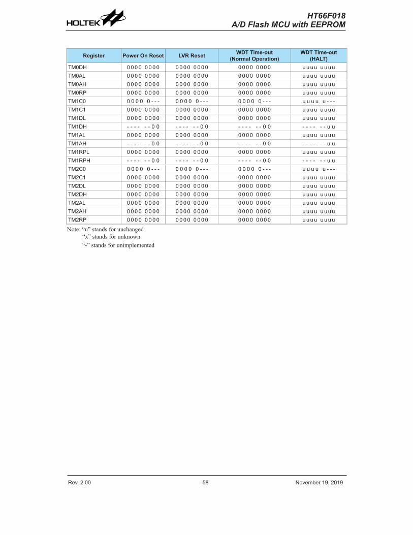
Rev. 2.00 58 November 19, 2019 Rev. 2.00 59 November 19, 2019
HT66F018A/D Flash MCU with EEPROM
HT66F018A/D Flash MCU with EEPROM
Register Power On Reset LVR Reset WDT Time-out(Normal Operation)
WDT Time-out(HALT)
TM0DH 0 0 0 0 0 0 0 0 0 0 0 0 0 0 0 0 0 0 0 0 0 0 0 0 u u u u u u u uTM0AL 0 0 0 0 0 0 0 0 0 0 0 0 0 0 0 0 0 0 0 0 0 0 0 0 u u u u u u u uTM0AH 0 0 0 0 0 0 0 0 0 0 0 0 0 0 0 0 0 0 0 0 0 0 0 0 u u u u u u u uTM0RP 0 0 0 0 0 0 0 0 0 0 0 0 0 0 0 0 0 0 0 0 0 0 0 0 u u u u u u u uTM1C0 0 0 0 0 0 - - - 0 0 0 0 0 - - - 0 0 0 0 0 - - - u u u u u - - -TM1C1 0 0 0 0 0 0 0 0 0 0 0 0 0 0 0 0 0 0 0 0 0 0 0 0 u u u u u u u uTM1DL 0 0 0 0 0 0 0 0 0 0 0 0 0 0 0 0 0 0 0 0 0 0 0 0 u u u u u u u uTM1DH - - - - - - 0 0 - - - - - - 0 0 - - - - - - 0 0 - - - - - - u uTM1AL 0 0 0 0 0 0 0 0 0 0 0 0 0 0 0 0 0 0 0 0 0 0 0 0 u u u u u u u uTM1AH - - - - - - 0 0 - - - - - - 0 0 - - - - - - 0 0 - - - - - - u uTM1RPL 0 0 0 0 0 0 0 0 0 0 0 0 0 0 0 0 0 0 0 0 0 0 0 0 u u u u u u u uTM1RPH - - - - - - 0 0 - - - - - - 0 0 - - - - - - 0 0 - - - - - - u uTM2C0 0 0 0 0 0 - - - 0 0 0 0 0 - - - 0 0 0 0 0 - - - u u u u u - - -TM2C1 0 0 0 0 0 0 0 0 0 0 0 0 0 0 0 0 0 0 0 0 0 0 0 0 u u u u u u u uTM2DL 0 0 0 0 0 0 0 0 0 0 0 0 0 0 0 0 0 0 0 0 0 0 0 0 u u u u u u u uTM2DH 0 0 0 0 0 0 0 0 0 0 0 0 0 0 0 0 0 0 0 0 0 0 0 0 u u u u u u u uTM2AL 0 0 0 0 0 0 0 0 0 0 0 0 0 0 0 0 0 0 0 0 0 0 0 0 u u u u u u u uTM2AH 0 0 0 0 0 0 0 0 0 0 0 0 0 0 0 0 0 0 0 0 0 0 0 0 u u u u u u u uTM2RP 0 0 0 0 0 0 0 0 0 0 0 0 0 0 0 0 0 0 0 0 0 0 0 0 u u u u u u u u
Note: “u” stands for unchanged“x” stands for unknown “-” stands for unimplemented
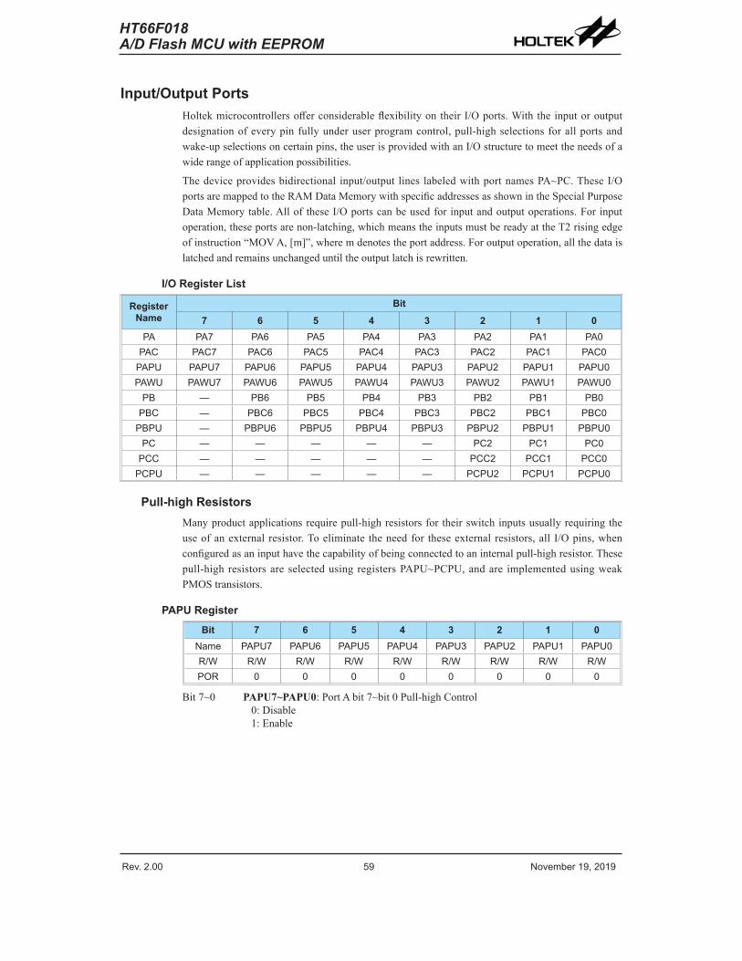
Rev. 2.00 58 November 19, 2019 Rev. 2.00 59 November 19, 2019
HT66F018A/D Flash MCU with EEPROM
HT66F018A/D Flash MCU with EEPROM
Input/Output Ports Holtek microcontrollers offer considerable flexibility on their I/O ports. With the input or output designation of every pin fully under user program control, pull-high selections for all ports and wake-up selections on certain pins, the user is provided with an I/O structure to meet the needs of a wide range of application possibilities.
The device provides bidirectional input/output lines labeled with port names PA~PC. These I/O ports are mapped to the RAM Data Memory with specific addresses as shown in the Special Purpose Data Memory table. All of these I/O ports can be used for input and output operations. For input operation, these ports are non-latching, which means the inputs must be ready at the T2 rising edge of instruction “MOV A, [m]”, where m denotes the port address. For output operation, all the data is latched and remains unchanged until the output latch is rewritten.
I/O Register List
Register Name
Bit7 6 5 4 3 2 1 0
PA PA7 PA6 PA5 PA4 PA3 PA2 PA1 PA0PAC PAC7 PAC6 PAC5 PAC4 PAC3 PAC2 PAC1 PAC0
PAPU PAPU7 PAPU6 PAPU5 PAPU4 PAPU3 PAPU2 PAPU1 PAPU0PAWU PAWU7 PAWU6 PAWU5 PAWU4 PAWU3 PAWU2 PAWU1 PAWU0
PB — PB6 PB5 PB4 PB3 PB2 PB1 PB0PBC — PBC6 PBC5 PBC4 PBC3 PBC2 PBC1 PBC0
PBPU — PBPU6 PBPU5 PBPU4 PBPU3 PBPU2 PBPU1 PBPU0PC — — — — — PC2 PC1 PC0
PCC — — — — — PCC2 PCC1 PCC0PCPU — — — — — PCPU2 PCPU1 PCPU0
Pull-high ResistorsMany product applications require pull-high resistors for their switch inputs usually requiring the use of an external resistor. To eliminate the need for these external resistors, all I/O pins, when configured as an input have the capability of being connected to an internal pull-high resistor. These pull-high resistors are selected using registers PAPU~PCPU, and are implemented using weak PMOS transistors.
PAPU RegisterBit 7 6 5 4 3 2 1 0
Name PAPU7 PAPU6 PAPU5 PAPU4 PAPU3 PAPU2 PAPU1 PAPU0R/W R/W R/W R/W R/W R/W R/W R/W R/WPOR 0 0 0 0 0 0 0 0
Bit 7~0 PAPU7~PAPU0: Port A bit 7~bit 0 Pull-high Control0: Disable1: Enable

Rev. 2.00 60 November 19, 2019 Rev. 2.00 61 November 19, 2019
HT66F018A/D Flash MCU with EEPROM
HT66F018A/D Flash MCU with EEPROM
PBPU RegisterBit 7 6 5 4 3 2 1 0
Name — PBPU6 PBPU5 PBPU4 PBPU3 PBPU2 PBPU1 PBPU0R/W — R/W R/W R/W R/W R/W R/W R/WPOR — 0 0 0 0 0 0 0
Bit 7 Unimplemented, read as “0”Bit 6~0 PBPU6~PBPU0: Port B bit 6~bit 0 Pull-high Control
0: Disable1: Enable
PCPU RegisterBit 7 6 5 4 3 2 1 0
Name — — — — — PCPU2 PCPU1 PCPU0R/W — — — — — R/W R/W R/WPOR — — — — — 0 0 0
Bit 7~3 Unimplemented, read as “0”Bit 2~0 PCPU2~PCPU0: Port C bit 3~bit 0 Pull-high Control
0: Disable1: Enable
Port A Wake-upThe HALT instruction forces the microcontroller into the SLEEP or IDLE Mode which preserves power, a feature that is important for battery and other low-power applications. Various methods exist to wake-up the microcontroller, one of which is to change the logic condition on one of the Port A pins from high to low. This function is especially suitable for applications that can be woken up via external switches. Each pin on Port A can be selected individually to have this wake-up feature using the PAWU register.
PAWU RegisterBit 7 6 5 4 3 2 1 0
Name PAWU7 PAWU6 PAWU5 PAWU4 PAWU3 PAWU2 PAWU1 PAWU0R/W R/W R/W R/W R/W R/W R/W R/W R/WPOR 0 0 0 0 0 0 0 0
Bit 7~0 PAWU7~PAWU0: Port A bit 7~bit 0 Wake-up Control0: Disable1: Enable
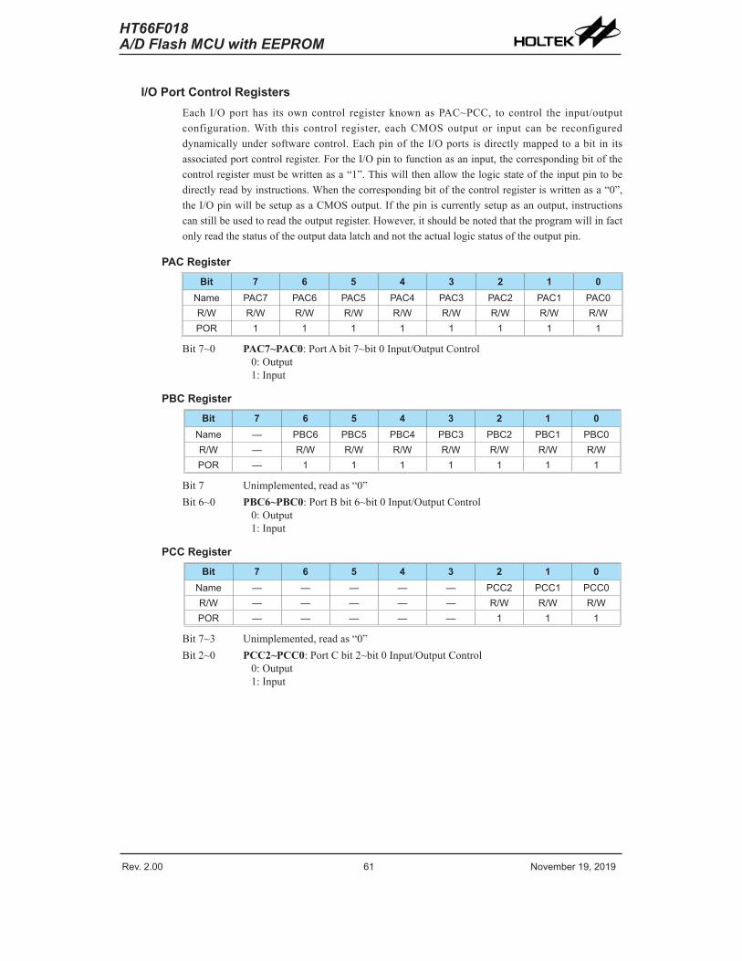
Rev. 2.00 60 November 19, 2019 Rev. 2.00 61 November 19, 2019
HT66F018A/D Flash MCU with EEPROM
HT66F018A/D Flash MCU with EEPROM
I/O Port Control RegistersEach I/O port has its own control register known as PAC~PCC, to control the input/output configuration. With this control register, each CMOS output or input can be reconfigured dynamically under software control. Each pin of the I/O ports is directly mapped to a bit in its associated port control register. For the I/O pin to function as an input, the corresponding bit of the control register must be written as a “1”. This will then allow the logic state of the input pin to be directly read by instructions. When the corresponding bit of the control register is written as a “0”, the I/O pin will be setup as a CMOS output. If the pin is currently setup as an output, instructions can still be used to read the output register. However, it should be noted that the program will in fact only read the status of the output data latch and not the actual logic status of the output pin.
PAC RegisterBit 7 6 5 4 3 2 1 0
Name PAC7 PAC6 PAC5 PAC4 PAC3 PAC2 PAC1 PAC0R/W R/W R/W R/W R/W R/W R/W R/W R/WPOR 1 1 1 1 1 1 1 1
Bit 7~0 PAC7~PAC0: Port A bit 7~bit 0 Input/Output Control0: Output1: Input
PBC RegisterBit 7 6 5 4 3 2 1 0
Name — PBC6 PBC5 PBC4 PBC3 PBC2 PBC1 PBC0R/W — R/W R/W R/W R/W R/W R/W R/WPOR — 1 1 1 1 1 1 1
Bit 7 Unimplemented, read as “0”Bit 6~0 PBC6~PBC0: Port B bit 6~bit 0 Input/Output Control
0: Output1: Input
PCC RegisterBit 7 6 5 4 3 2 1 0
Name — — — — — PCC2 PCC1 PCC0R/W — — — — — R/W R/W R/WPOR — — — — — 1 1 1
Bit 7~3 Unimplemented, read as “0”Bit 2~0 PCC2~PCC0: Port C bit 2~bit 0 Input/Output Control
0: Output1: Input
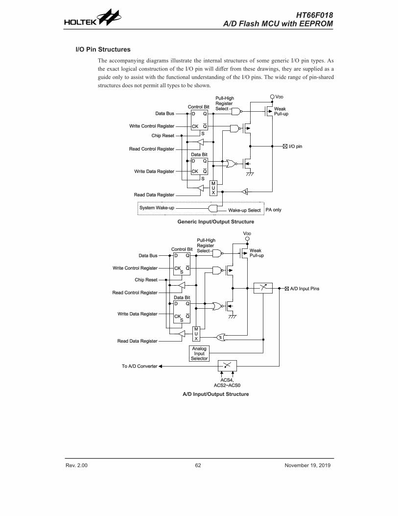
Rev. 2.00 62 November 19, 2019 Rev. 2.00 63 November 19, 2019
HT66F018A/D Flash MCU with EEPROM
HT66F018A/D Flash MCU with EEPROM
I/O Pin StructuresThe accompanying diagrams illustrate the internal structures of some generic I/O pin types. As the exact logical construction of the I/O pin will differ from these drawings, they are supplied as a guide only to assist with the functional understanding of the I/O pins. The wide range of pin-shared structures does not permit all types to be shown.
Generic Input/Output Structure
A/D Input/Output Structure
Rev. 2.00 62 November 19, 2019 Rev. 2.00 63 November 19, 2019
HT66F018A/D Flash MCU with EEPROM
HT66F018A/D Flash MCU with EEPROM
Programming Considerations Within the user program, one of the first things to consider is port initialisation. After a reset, all of the I/O data and port control registers will be set high. This means that all I/O pins will default to an input state, the level of which depends on the other connected circuitry and whether pull-high selections have been chosen. If the port control registers, PAC~PCC, are then programmed to setup some pins as outputs, these output pins will have an initial high output value unless the associated port data registers, PA~PC, are first programmed. Selecting which pins are inputs and which are outputs can be achieved byte-wide by loading the correct values into the appropriate port control register or by programming individual bits in the port control register using the “SET [m].i” and “CLR [m].i” instructions. Note that when using these bit control instructions, a read-modify-write operation takes place. The microcontroller must first read in the data on the entire port, modify it to the required new bit values and then rewrite this data back to the output ports.
The power-on reset condition of the A/D converter control registers ensures that any A/D input pins, which are always shared with other I/O functions - will be setup as analog inputs after a reset. Although these pins will be configured as A/D inputs after a reset, the A/D converter will not be switched on. It is therefore important to note that if it is required to use these pins as I/O digital input pins or as other functions, the A/D converter control registers must be correctly programmed to remove the A/D function. Note also that as the A/D channel is enabled, any internal pull-high resistor connections will be removed.
Port A has the additional capability of providing wake-up functions. When the device is in the SLEEP or IDLE Mode, various methods are available to wake the device up. One of these is a high to low transition of any of the Port A pins. Single or multiple pins on Port A can be setup to have this function.

Rev. 2.00 64 November 19, 2019 Rev. 2.00 65 November 19, 2019
HT66F018A/D Flash MCU with EEPROM
HT66F018A/D Flash MCU with EEPROM
Timer Modules – TMOne of the most fundamental functions in any microcontroller device is the ability to control and measure time. To implement time related functions each device includes several Timer Modules, abbreviated to the name TM. The TMs are multi-purpose timing units and serve to provide operations such as Timer/Counter, Input Capture, Compare Match Output and Single Pulse Output as well as being the functional unit for the generation of PWM signals. Each of the TMs has two individual interrupts. The addition of input and output pins for each TM ensures that users are provided with timing units with a wide and flexible range of features.
The common features of the different TM types are described here with more detailed information provided in the individual Compact, Standard and Periodic TM sections.
IntroductionThe device contains three TMs having a reference name of TM0, TM1, and TM2. Each individual TM can be categorised as a certain type, namely Compact Type TM, Standard Type TM or Periodic Type TM. Although similar in nature, the different TM types vary in their feature complexity. The common features to all of the Compact, Standard and Periodic TMs will be described in this section and the detailed operation regarding each of the TM types will be described in separate sections. The main features and differences between the three types of TMs are summarised in the accompanying table.
Function CTM STM PTMTimer/Counter √ √ √I/P Capture — √ √Compare Match Output √ √ √PWM Channels 1 1 1Single Pulse Output — 1 1PWM Alignment Edge Edge EdgePWM Adjustment Period & Duty Duty or Period Duty or Period Duty or Period
This chip contains a specific number of either Compact Type, Standard Type and Periodic Type TM units which are shown in the table together with their individual reference names, TM0~TM2.
Device TM0 TM1 TM2HT66F018 16-bit STM 10-bit PTM 16-bit CTM
TM Name/Type Reference
TM OperationThe three different types of TM offer a diverse range of functions, from simple timing operations to PWM signal generation. The key to understanding how the TM operates is to see it in terms of a free running counter whose value is then compared with the value of pre-programmed internal comparators. When the free running counter has the same value as the pre-programmed comparator, known as a compare match situation, a TM interrupt signal will be generated which can clear the counter and perhaps also change the condition of the TM output pin. The internal TM counter is driven by a user selectable clock source, which can be an internal clock or an external pin.
Rev. 2.00 64 November 19, 2019 Rev. 2.00 65 November 19, 2019
HT66F018A/D Flash MCU with EEPROM
HT66F018A/D Flash MCU with EEPROM
TM Clock SourceThe clock source which drives the main counter in each TM can originate from various sources. The selection of the required clock source is implemented using the TnCK2~TnCK0 bits in the TM control registers. The clock source can be a ratio of either the system clock fSYS or the internal high clock fH, the fTBC clock source or the external TCKn pin. Note that setting these bits to the value 101 will select a reserved clock input, in effect disconnecting the TM clock source. The TCKn pin clock source is used to allow an external signal to drive the TM as an external clock source or for event counting.
TM InterruptsThe Compact Type, Standard Type and Periodic Type TMs each have two internal interrupts, one for each of the internal comparator A or comparator P, which generate a TM interrupt when a compare match condition occurs. When a TM interrupt is generated it can be used to clear the counter and also to change the state of the TM output pin.
TM External Pins Each of the TMs, irrespective of what type, has one TM input pin, with the label TCKn. The TM input pin is essentially a clock source for the TM and is selected using the TnCK2~TnCK0 bits in the TMnC0 register. This external TM input pin allows an external clock source to drive the internal TM. This external TM input pin is shared with other functions but will be connected to the internal TM if selected using the TnCK2~TnCK0 bits. The TM input pin can be chosen to have either a rising or falling active edge.
The TMs each have one output pin with the label TPn. When the TM is in the Compare Match Output Mode, these pins can be controlled by the TM to switch to a high or low level or to toggle when a compare match situation occurs. The external TPn output pin is also the pin where the TM generates the PWM output waveform. The TPn pin acts as an input when the TM is setup to operate in the Capture Input Mode. As the TPn pins are pin-shared with other functions, the TPn pin function is enabled or disabled according to the internal TM on/off control, operation mode and output control settings. When the corresponding TM configuration selects the TPn pin to be used as an output pin, the associated pin will be setup as an external TM output pin. If the TM configuration selects the TPn pin to be setup as an input pin, the input signal supplied on the associated pin can be derived from an external signal and other pin-shared output function. If the TM configuration determines that the TPn pin function is not used, the associated pin will be controlled by other pin-shared functions. The details of the TPn pin for each TM type and device are provided in the accompanying table.
CTM STM PTM RegisterTP2 TP0 TP1 TMPC
TM Output Pins
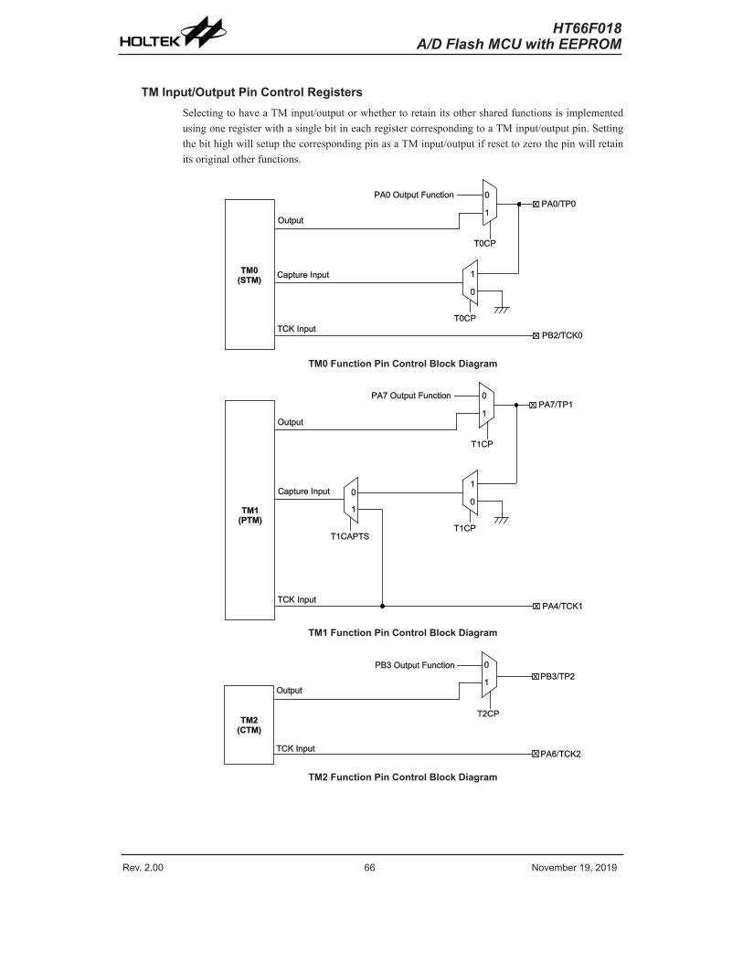
Rev. 2.00 66 November 19, 2019 Rev. 2.00 67 November 19, 2019
HT66F018A/D Flash MCU with EEPROM
HT66F018A/D Flash MCU with EEPROM
TM Input/Output Pin Control RegistersSelecting to have a TM input/output or whether to retain its other shared functions is implemented using one register with a single bit in each register corresponding to a TM input/output pin. Setting the bit high will setup the corresponding pin as a TM input/output if reset to zero the pin will retain its original other functions.
TM0 Function Pin Control Block Diagram
TM1 Function Pin Control Block Diagram
TM2 Function Pin Control Block Diagram
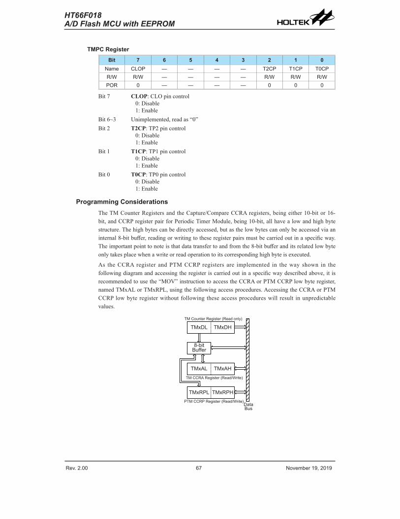
Rev. 2.00 66 November 19, 2019 Rev. 2.00 67 November 19, 2019
HT66F018A/D Flash MCU with EEPROM
HT66F018A/D Flash MCU with EEPROM
TMPC RegisterBit 7 6 5 4 3 2 1 0
Name CLOP — — — — T2CP T1CP T0CPR/W R/W — — — — R/W R/W R/WPOR 0 — — — — 0 0 0
Bit 7 CLOP: CLO pin control0: Disable1: Enable
Bit 6~3 Unimplemented, read as “0”Bit 2 T2CP: TP2 pin control
0: Disable1: Enable
Bit 1 T1CP: TP1 pin control0: Disable1: Enable
Bit 0 T0CP: TP0 pin control0: Disable1: Enable
Programming ConsiderationsThe TM Counter Registers and the Capture/Compare CCRA registers, being either 10-bit or 16-bit, and CCRP register pair for Periodic Timer Module, being 10-bit, all have a low and high byte structure. The high bytes can be directly accessed, but as the low bytes can only be accessed via an internal 8-bit buffer, reading or writing to these register pairs must be carried out in a specific way. The important point to note is that data transfer to and from the 8-bit buffer and its related low byte only takes place when a write or read operation to its corresponding high byte is executed.
As the CCRA register and PTM CCRP registers are implemented in the way shown in the following diagram and accessing the register is carried out in a specific way described above, it is recommended to use the “MOV” instruction to access the CCRA or PTM CCRP low byte register, named TMxAL or TMxRPL, using the following access procedures. Accessing the CCRA or PTM CCRP low byte register without following these access procedures will result in unpredictable values.
Data Bus
8-bit Buffer
TMxDHTMxDL
TMxRPHTMxRPL
TMxAHTMxAL
TM Counter Register (Read only)
TM CCRA Register (Read/Write)
PTM CCRP Register (Read/Write)
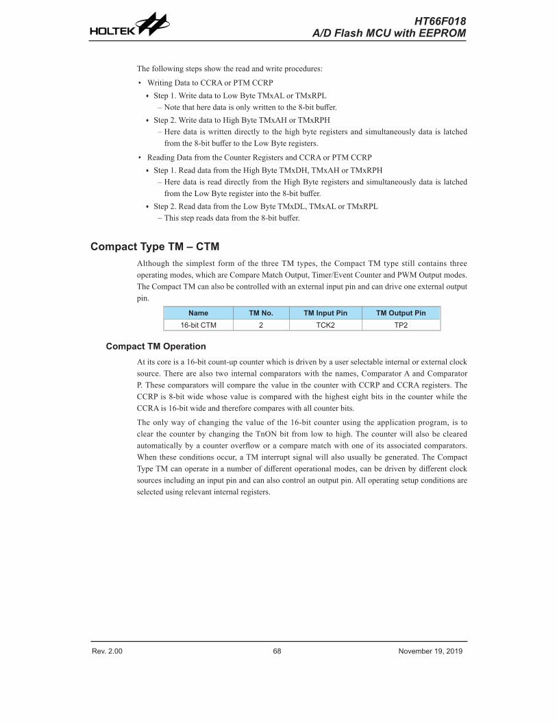
Rev. 2.00 68 November 19, 2019 Rev. 2.00 69 November 19, 2019
HT66F018A/D Flash MCU with EEPROM
HT66F018A/D Flash MCU with EEPROM
The following steps show the read and write procedures:
• Writing Data to CCRA or PTM CCRP ♦ Step 1. Write data to Low Byte TMxAL or TMxRPL
– Note that here data is only written to the 8-bit buffer. ♦ Step 2. Write data to High Byte TMxAH or TMxRPH
– Here data is written directly to the high byte registers and simultaneously data is latched from the 8-bit buffer to the Low Byte registers.
• Reading Data from the Counter Registers and CCRA or PTM CCRP ♦ Step 1. Read data from the High Byte TMxDH, TMxAH or TMxRPH
– Here data is read directly from the High Byte registers and simultaneously data is latched from the Low Byte register into the 8-bit buffer.
♦ Step 2. Read data from the Low Byte TMxDL, TMxAL or TMxRPL – This step reads data from the 8-bit buffer.
Compact Type TM – CTMAlthough the simplest form of the three TM types, the Compact TM type still contains three operating modes, which are Compare Match Output, Timer/Event Counter and PWM Output modes. The Compact TM can also be controlled with an external input pin and can drive one external output pin.
Name TM No. TM Input Pin TM Output Pin16-bit CTM 2 TCK2 TP2
Compact TM OperationAt its core is a 16-bit count-up counter which is driven by a user selectable internal or external clock source. There are also two internal comparators with the names, Comparator A and Comparator P. These comparators will compare the value in the counter with CCRP and CCRA registers. The CCRP is 8-bit wide whose value is compared with the highest eight bits in the counter while the CCRA is 16-bit wide and therefore compares with all counter bits.
The only way of changing the value of the 16-bit counter using the application program, is to clear the counter by changing the TnON bit from low to high. The counter will also be cleared automatically by a counter overflow or a compare match with one of its associated comparators. When these conditions occur, a TM interrupt signal will also usually be generated. The Compact Type TM can operate in a number of different operational modes, can be driven by different clock sources including an input pin and can also control an output pin. All operating setup conditions are selected using relevant internal registers.
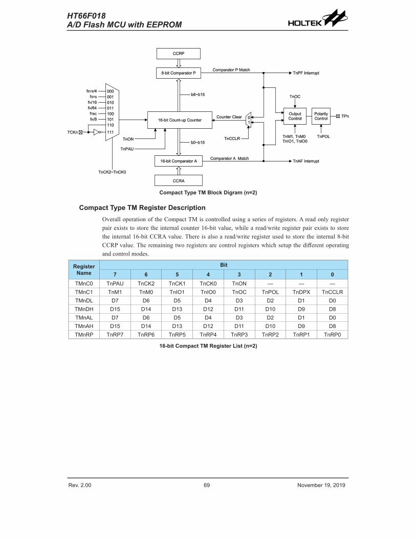
Rev. 2.00 68 November 19, 2019 Rev. 2.00 69 November 19, 2019
HT66F018A/D Flash MCU with EEPROM
HT66F018A/D Flash MCU with EEPROM
Compact Type TM Block Digram (n=2)
Compact Type TM Register DescriptionOverall operation of the Compact TM is controlled using a series of registers. A read only register pair exists to store the internal counter 16-bit value, while a read/write register pair exists to store the internal 16-bit CCRA value. There is also a read/write register used to store the internal 8-bit CCRP value. The remaining two registers are control registers which setup the different operating and control modes.
Register Name
Bit7 6 5 4 3 2 1 0
TMnC0 TnPAU TnCK2 TnCK1 TnCK0 TnON — — —TMnC1 TnM1 TnM0 TnIO1 TnIO0 TnOC TnPOL TnDPX TnCCLRTMnDL D7 D6 D5 D4 D3 D2 D1 D0TMnDH D15 D14 D13 D12 D11 D10 D9 D8TMnAL D7 D6 D5 D4 D3 D2 D1 D0TMnAH D15 D14 D13 D12 D11 D10 D9 D8TMnRP TnRP7 TnRP6 TnRP5 TnRP4 TnRP3 TnRP2 TnRP1 TnRP0
16-bit Compact TM Register List (n=2)
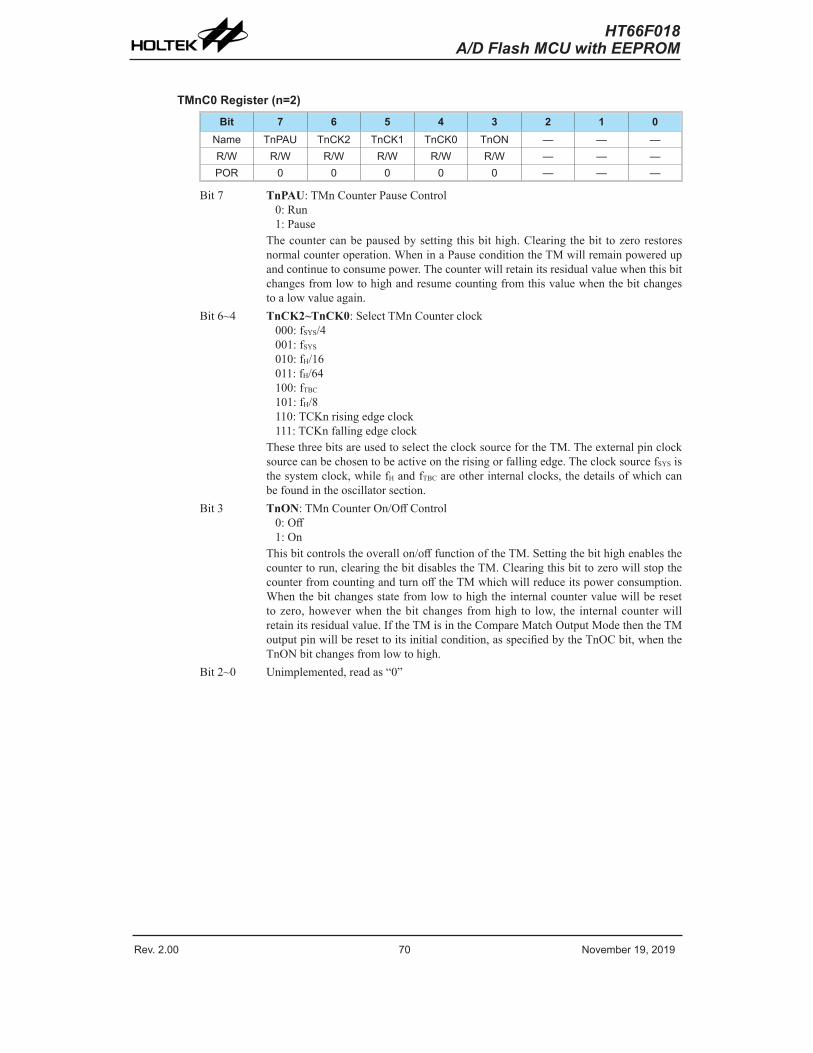
Rev. 2.00 70 November 19, 2019 Rev. 2.00 71 November 19, 2019
HT66F018A/D Flash MCU with EEPROM
HT66F018A/D Flash MCU with EEPROM
TMnC0 Register (n=2)Bit 7 6 5 4 3 2 1 0
Name TnPAU TnCK2 TnCK1 TnCK0 TnON — — —R/W R/W R/W R/W R/W R/W — — —POR 0 0 0 0 0 — — —
Bit 7 TnPAU: TMn Counter Pause Control0: Run1: Pause
The counter can be paused by setting this bit high. Clearing the bit to zero restores normal counter operation. When in a Pause condition the TM will remain powered up and continue to consume power. The counter will retain its residual value when this bit changes from low to high and resume counting from this value when the bit changes to a low value again.
Bit 6~4 TnCK2~TnCK0: Select TMn Counter clock000: fSYS/4001: fSYS
010: fH/16011: fH/64100: fTBC
101: fH/8110: TCKn rising edge clock111: TCKn falling edge clock
These three bits are used to select the clock source for the TM. The external pin clock source can be chosen to be active on the rising or falling edge. The clock source fSYS is the system clock, while fH and fTBC are other internal clocks, the details of which can be found in the oscillator section.
Bit 3 TnON: TMn Counter On/Off Control0: Off1: On
This bit controls the overall on/off function of the TM. Setting the bit high enables the counter to run, clearing the bit disables the TM. Clearing this bit to zero will stop the counter from counting and turn off the TM which will reduce its power consumption. When the bit changes state from low to high the internal counter value will be reset to zero, however when the bit changes from high to low, the internal counter will retain its residual value. If the TM is in the Compare Match Output Mode then the TM output pin will be reset to its initial condition, as specified by the TnOC bit, when the TnON bit changes from low to high.
Bit 2~0 Unimplemented, read as “0”
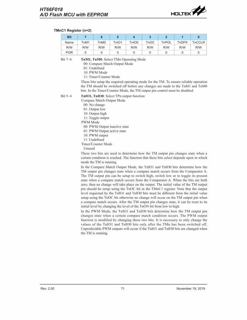
Rev. 2.00 70 November 19, 2019 Rev. 2.00 71 November 19, 2019
HT66F018A/D Flash MCU with EEPROM
HT66F018A/D Flash MCU with EEPROM
TMnC1 Register (n=2)Bit 7 6 5 4 3 2 1 0
Name TnM1 TnM0 TnIO1 TnIO0 TnOC TnPOL TnDPX TnCCLRR/W R/W R/W R/W R/W R/W R/W R/W R/WPOR 0 0 0 0 0 0 0 0
Bit 7~6 TnM1, TnM0: Select TMn Operating Mode00: Compare Match Output Mode01: Undefined10: PWM Mode11: Timer/Counter Mode
These bits setup the required operating mode for the TM. To ensure reliable operation the TM should be switched off before any changes are made to the TnM1 and TnM0 bits. In the Timer/Counter Mode, the TM output pin control must be disabled.
Bit 5~4 TnIO1, TnIO0: Select TPn output functionCompare Match Output Mode
00: No change01: Output low10: Output high11: Toggle output
PWM Mode00: PWM Output inactive state01: PWM Output active state10: PWM output11: Undefined
Timer/Counter Mode Unused
These two bits are used to determine how the TM output pin changes state when a certain condition is reached. The function that these bits select depends upon in which mode the TM is running.In the Compare Match Output Mode, the TnIO1 and TnIO0 bits determine how the TM output pin changes state when a compare match occurs from the Comparator A. The TM output pin can be setup to switch high, switch low or to toggle its present state when a compare match occurs from the Comparator A. When the bits are both zero, then no change will take place on the output. The initial value of the TM output pin should be setup using the TnOC bit in the TMnC1 register. Note that the output level requested by the TnIO1 and TnIO0 bits must be different from the initial value setup using the TnOC bit otherwise no change will occur on the TM output pin when a compare match occurs. After the TM output pin changes state, it can be reset to its initial level by changing the level of the TnON bit from low to high.In the PWM Mode, the TnIO1 and TnIO0 bits determine how the TM output pin changes state when a certain compare match condition occurs. The PWM output function is modified by changing these two bits. It is necessary to only change the values of the TnIO1 and TnIO0 bits only after the TMn has been switched off. Unpredictable PWM outputs will occur if the TnIO1 and TnIO0 bits are changed when the TM is running.
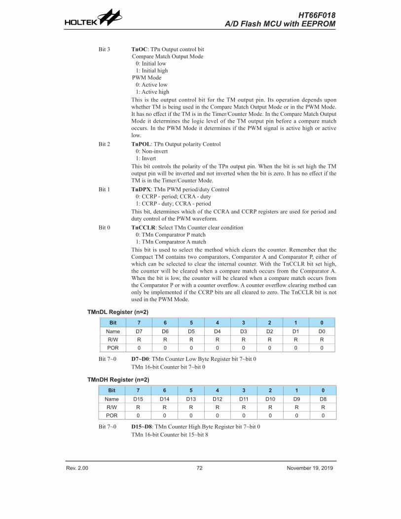
Rev. 2.00 72 November 19, 2019 Rev. 2.00 73 November 19, 2019
HT66F018A/D Flash MCU with EEPROM
HT66F018A/D Flash MCU with EEPROM
Bit 3 TnOC: TPn Output control bitCompare Match Output Mode
0: Initial low1: Initial high
PWM Mode0: Active low1: Active high
This is the output control bit for the TM output pin. Its operation depends upon whether TM is being used in the Compare Match Output Mode or in the PWM Mode. It has no effect if the TM is in the Timer/Counter Mode. In the Compare Match Output Mode it determines the logic level of the TM output pin before a compare match occurs. In the PWM Mode it determines if the PWM signal is active high or active low.
Bit 2 TnPOL: TPn Output polarity Control0: Non-invert1: Invert
This bit controls the polarity of the TPn output pin. When the bit is set high the TM output pin will be inverted and not inverted when the bit is zero. It has no effect if the TM is in the Timer/Counter Mode.
Bit 1 TnDPX: TMn PWM period/duty Control0: CCRP - period; CCRA - duty1: CCRP - duty; CCRA - period
This bit, determines which of the CCRA and CCRP registers are used for period and duty control of the PWM waveform.
Bit 0 TnCCLR: Select TMn Counter clear condition0: TMn Comparatror P match1: TMn Comparatror A match
This bit is used to select the method which clears the counter. Remember that the Compact TM contains two comparators, Comparator A and Comparator P, either of which can be selected to clear the internal counter. With the TnCCLR bit set high, the counter will be cleared when a compare match occurs from the Comparator A. When the bit is low, the counter will be cleared when a compare match occurs from the Comparator P or with a counter overflow. A counter overflow clearing method can only be implemented if the CCRP bits are all cleared to zero. The TnCCLR bit is not used in the PWM Mode.
TMnDL Register (n=2)Bit 7 6 5 4 3 2 1 0
Name D7 D6 D5 D4 D3 D2 D1 D0R/W R R R R R R R RPOR 0 0 0 0 0 0 0 0
Bit 7~0 D7~D0: TMn Counter Low Byte Register bit 7~bit 0TMn 16-bit Counter bit 7~bit 0
TMnDH Register (n=2)Bit 7 6 5 4 3 2 1 0
Name D15 D14 D13 D12 D11 D10 D9 D8R/W R R R R R R R RPOR 0 0 0 0 0 0 0 0
Bit 7~0 D15~D8: TMn Counter High Byte Register bit 7~bit 0TMn 16-bit Counter bit 15~bit 8
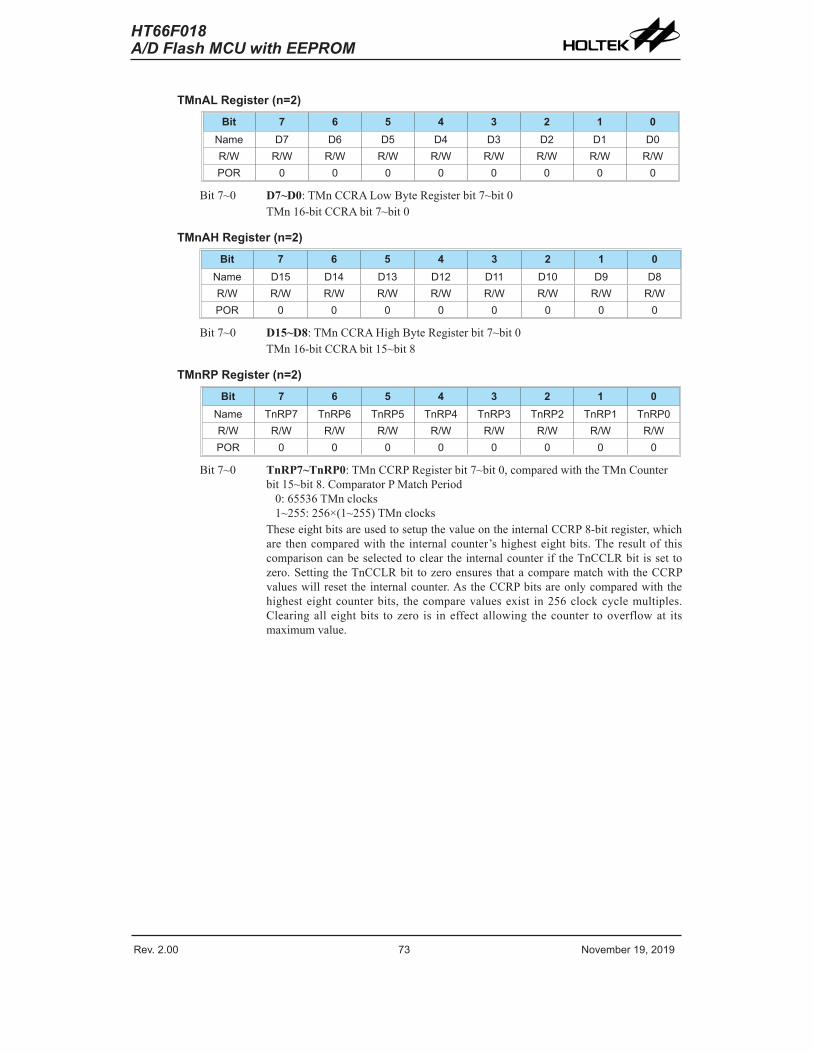
Rev. 2.00 72 November 19, 2019 Rev. 2.00 73 November 19, 2019
HT66F018A/D Flash MCU with EEPROM
HT66F018A/D Flash MCU with EEPROM
TMnAL Register (n=2)Bit 7 6 5 4 3 2 1 0
Name D7 D6 D5 D4 D3 D2 D1 D0R/W R/W R/W R/W R/W R/W R/W R/W R/WPOR 0 0 0 0 0 0 0 0
Bit 7~0 D7~D0: TMn CCRA Low Byte Register bit 7~bit 0TMn 16-bit CCRA bit 7~bit 0
TMnAH Register (n=2)Bit 7 6 5 4 3 2 1 0
Name D15 D14 D13 D12 D11 D10 D9 D8R/W R/W R/W R/W R/W R/W R/W R/W R/WPOR 0 0 0 0 0 0 0 0
Bit 7~0 D15~D8: TMn CCRA High Byte Register bit 7~bit 0TMn 16-bit CCRA bit 15~bit 8
TMnRP Register (n=2)Bit 7 6 5 4 3 2 1 0
Name TnRP7 TnRP6 TnRP5 TnRP4 TnRP3 TnRP2 TnRP1 TnRP0R/W R/W R/W R/W R/W R/W R/W R/W R/WPOR 0 0 0 0 0 0 0 0
Bit 7~0 TnRP7~TnRP0: TMn CCRP Register bit 7~bit 0, compared with the TMn Counter bit 15~bit 8. Comparator P Match Period
0: 65536 TMn clocks1~255: 256×(1~255) TMn clocks
These eight bits are used to setup the value on the internal CCRP 8-bit register, which are then compared with the internal counter’s highest eight bits. The result of this comparison can be selected to clear the internal counter if the TnCCLR bit is set to zero. Setting the TnCCLR bit to zero ensures that a compare match with the CCRP values will reset the internal counter. As the CCRP bits are only compared with the highest eight counter bits, the compare values exist in 256 clock cycle multiples. Clearing all eight bits to zero is in effect allowing the counter to overflow at its maximum value.
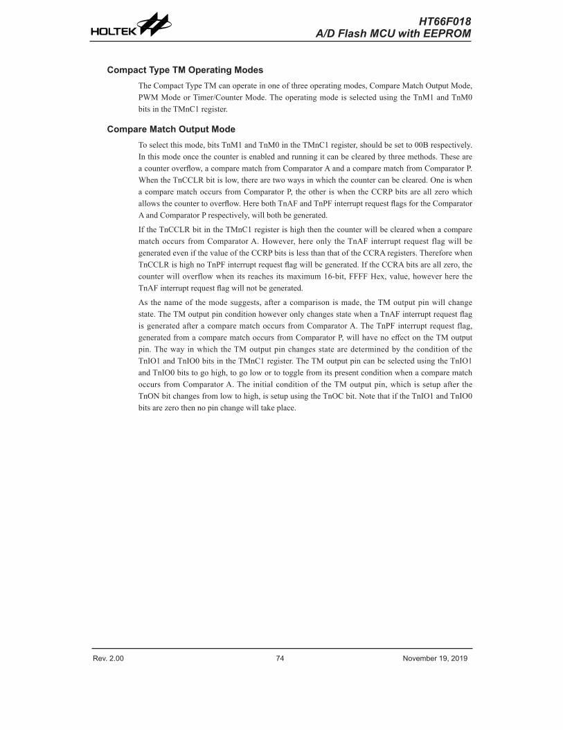
Rev. 2.00 74 November 19, 2019 Rev. 2.00 75 November 19, 2019
HT66F018A/D Flash MCU with EEPROM
HT66F018A/D Flash MCU with EEPROM
Compact Type TM Operating ModesThe Compact Type TM can operate in one of three operating modes, Compare Match Output Mode, PWM Mode or Timer/Counter Mode. The operating mode is selected using the TnM1 and TnM0 bits in the TMnC1 register.
Compare Match Output ModeTo select this mode, bits TnM1 and TnM0 in the TMnC1 register, should be set to 00B respectively. In this mode once the counter is enabled and running it can be cleared by three methods. These are a counter overflow, a compare match from Comparator A and a compare match from Comparator P. When the TnCCLR bit is low, there are two ways in which the counter can be cleared. One is when a compare match occurs from Comparator P, the other is when the CCRP bits are all zero which allows the counter to overflow. Here both TnAF and TnPF interrupt request flags for the Comparator A and Comparator P respectively, will both be generated.
If the TnCCLR bit in the TMnC1 register is high then the counter will be cleared when a compare match occurs from Comparator A. However, here only the TnAF interrupt request flag will be generated even if the value of the CCRP bits is less than that of the CCRA registers. Therefore when TnCCLR is high no TnPF interrupt request flag will be generated. If the CCRA bits are all zero, the counter will overflow when its reaches its maximum 16-bit, FFFF Hex, value, however here the TnAF interrupt request flag will not be generated.
As the name of the mode suggests, after a comparison is made, the TM output pin will change state. The TM output pin condition however only changes state when a TnAF interrupt request flag is generated after a compare match occurs from Comparator A. The TnPF interrupt request flag, generated from a compare match occurs from Comparator P, will have no effect on the TM output pin. The way in which the TM output pin changes state are determined by the condition of the TnIO1 and TnIO0 bits in the TMnC1 register. The TM output pin can be selected using the TnIO1 and TnIO0 bits to go high, to go low or to toggle from its present condition when a compare match occurs from Comparator A. The initial condition of the TM output pin, which is setup after the TnON bit changes from low to high, is setup using the TnOC bit. Note that if the TnIO1 and TnIO0 bits are zero then no pin change will take place.
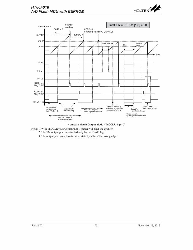
Rev. 2.00 74 November 19, 2019 Rev. 2.00 75 November 19, 2019
HT66F018A/D Flash MCU with EEPROM
HT66F018A/D Flash MCU with EEPROM
CCRA
CCRP
0xFFFF
Counter overflow
CCRA Int.Flag TnAF
CCRP Int.Flag TnPF
CCRP > 0Counter cleared by CCRP value
TM O/P Pin
TnON
Pause CounterReset
Output Pin set to Initial LevelLow if TnOC = 0
Output Togglewith TnAF flag
Here TnIO [1:0] = 11Toggle Output Select
Now TnIO [1:0] = 10 Active High Output Select
Output not affected byTnAF flag. Remains Highuntil reset by TnON bit
TnCCLR = 0; TnM [1:0] = 00
TnPAU
ResumeStop
Time
CCRP > 0
CCRP = 0
TnPOL
Output PinReset to initial value
Output invertswhen TnPOL is high
Output controlledby other pin-shared function
Counter Value
Compare Match Output Mode - TnCCLR=0 (n=2)Note: 1. With TnCCLR=0, a Comparator P match will clear the counter
2. The TM output pin is controlled only by the TnAF flag3. The output pin is reset to its initial state by a TnON bit rising edge
Rev. 2.00 76 November 19, 2019 Rev. 2.00 77 November 19, 2019
HT66F018A/D Flash MCU with EEPROM
HT66F018A/D Flash MCU with EEPROM
CCRP
CCRA
0xFFFF
CCRA = 0Counter overflows
CCRP Int.Flag TnPF
CCRA Int.Flag TnAF
CCRA > 0 Counter cleared by CCRA value
TM O/P Pin
TnON bit
Pause CounterReset
Output PinReset to initial value
Output Pin set to Initial LevelLow if TnOC = 0
Output Togglewith TnAF flag
Here TnIO[1:0] = 11Toggle Output Select
Now TnIO[1:0] = 10 Active High Output Select
TnPAU bit
ResumeStop
Time
TnPF notgenerated
No TnAF flaggenerated on CCRA overflow
Output doesnot change
CCRA = 0
Output invertswhen TnPOL is high
TnPOL bit
TnCCLR = 1; TnM[1:0] = 00
Output controlled byother pin-shared function
Output not affected byTnAF flag remains Highuntil reset by TnON bit
Counter Value
Compare Match Output Mode - TnCCLR=1 (n=2)Note: 1. With TnCCLR=1, a Comparator A match will clear the counter
2. The TM output pin is controlled only by the TnAF flag3. The output pin is reset to its initial state by a TnON bit rising edge4. The TnPF flag is not generated when TnCCLR=1
Timer/Counter Mode To select this mode, bits TnM1 and TnM0 in the TMnC1 register should be set to 11 respectively. The Timer/Counter Mode operates in an identical way to the Compare Match Output Mode generating the same interrupt flags. The exception is that in the Timer/Counter Mode the TM output pin is not used. Therefore the above description and Timing Diagrams for the Compare Match Output Mode can be used to understand its function. As the TM output pin is not used in this mode, the pin can be used as a normal I/O pin or other pin-shared function.
Rev. 2.00 76 November 19, 2019 Rev. 2.00 77 November 19, 2019
HT66F018A/D Flash MCU with EEPROM
HT66F018A/D Flash MCU with EEPROM
PWM Output Mode To select this mode, bits TnM1 and TnM0 in the TMnC1 register should be set to 10 respectively. The PWM function within the TM is useful for applications which require functions such as motor control, heating control, illumination control etc. By providing a signal of fixed frequency but of varying duty cycle on the TM output pin, a square wave AC waveform can be generated with varying equivalent DC RMS values.
As both the period and duty cycle of the PWM waveform can be controlled, the choice of generated waveform is extremely flexible. In the PWM mode, the TnCCLR bit has no effect on the PWM operation. Both of the CCRA and CCRP registers are used to generate the PWM waveform, one register is used to clear the internal counter and thus control the PWM waveform frequency, while the other one is used to control the duty cycle. Which register is used to control either frequency or duty cycle is determined using the TnDPX bit in the TMnC1 register. The PWM waveform frequency and duty cycle can therefore be controlled by the values in the CCRA and CCRP registers.
An interrupt flag, one for each of the CCRA and CCRP, will be generated when a compare match occurs from either Comparator A or Comparator P. The TnOC bit in the TMnC1 register is used to select the required polarity of the PWM waveform while the two TnIO1 and TnIO0 bits are used to enable the PWM output or to force the TM output pin to a fixed high or low level. The TnPOL bit is used to reverse the polarity of the PWM output waveform.
16-bit CTM, PWM Mode, Edge-aligned Mode, TnDPX=0CCRP 1~255 0Period CCRP×256 65536Duty CCRA
If fSYS=16MHz, TM clock source select fSYS/4, CCRP=2 and CCRA=128,
The STM PWM output frequency=(fSYS/4)/(2×256)=fSYS/2048=7.8125kHz, duty=128/(2×256)=25%.
If the Duty value defined by the CCRA register is equal to or greater than the Period value, then the PWM output duty is 100%.
16-bit CTM, PWM Mode, Edge-aligned Mode, TnDPX=1CCRP 1~255 0Period CCRADuty CCRP×256 65536
The PWM output period is determined by the CCRA register value together with the TM clock while the PWM duty cycle is defined by the (CCRP×256) except when the CCRP value is equal to 000b.
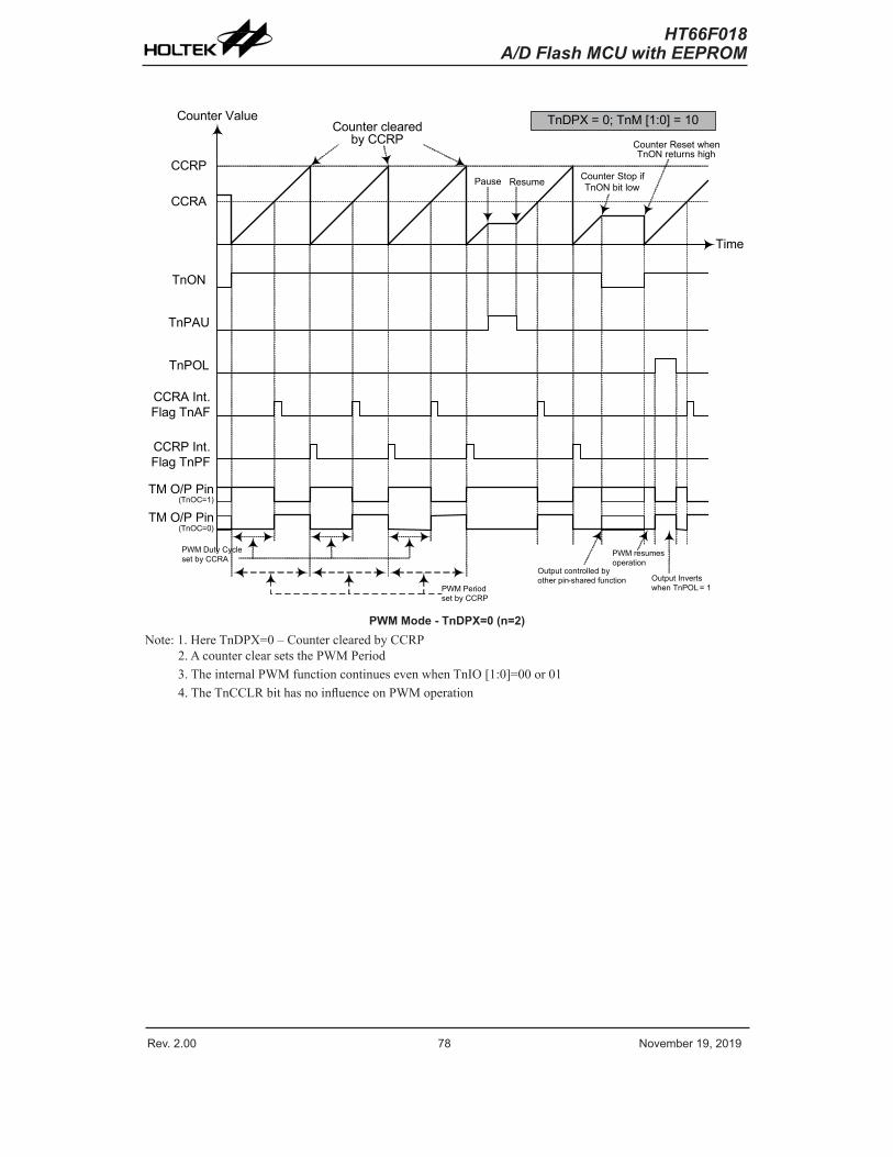
Rev. 2.00 78 November 19, 2019 Rev. 2.00 79 November 19, 2019
HT66F018A/D Flash MCU with EEPROM
HT66F018A/D Flash MCU with EEPROM
Counter Value
CCRP
CCRA
TnON
TnPAU
TnPOL
CCRP Int. Flag TnPF
CCRA Int. Flag TnAF
TM O/P Pin(TnOC=1)
Time
Counter cleared by CCRP
Pause Resume Counter Stop if TnON bit low
Counter Reset when TnON returns high
TnDPX = 0; TnM [1:0] = 10
PWM Duty Cycle set by CCRA
PWM resumes operation
Output controlled by other pin-shared function Output Inverts
when TnPOL = 1PWM Period set by CCRP
TM O/P Pin(TnOC=0)
PWM Mode - TnDPX=0 (n=2)Note: 1. Here TnDPX=0 – Counter cleared by CCRP
2. A counter clear sets the PWM Period3. The internal PWM function continues even when TnIO [1:0]=00 or 014. The TnCCLR bit has no influence on PWM operation
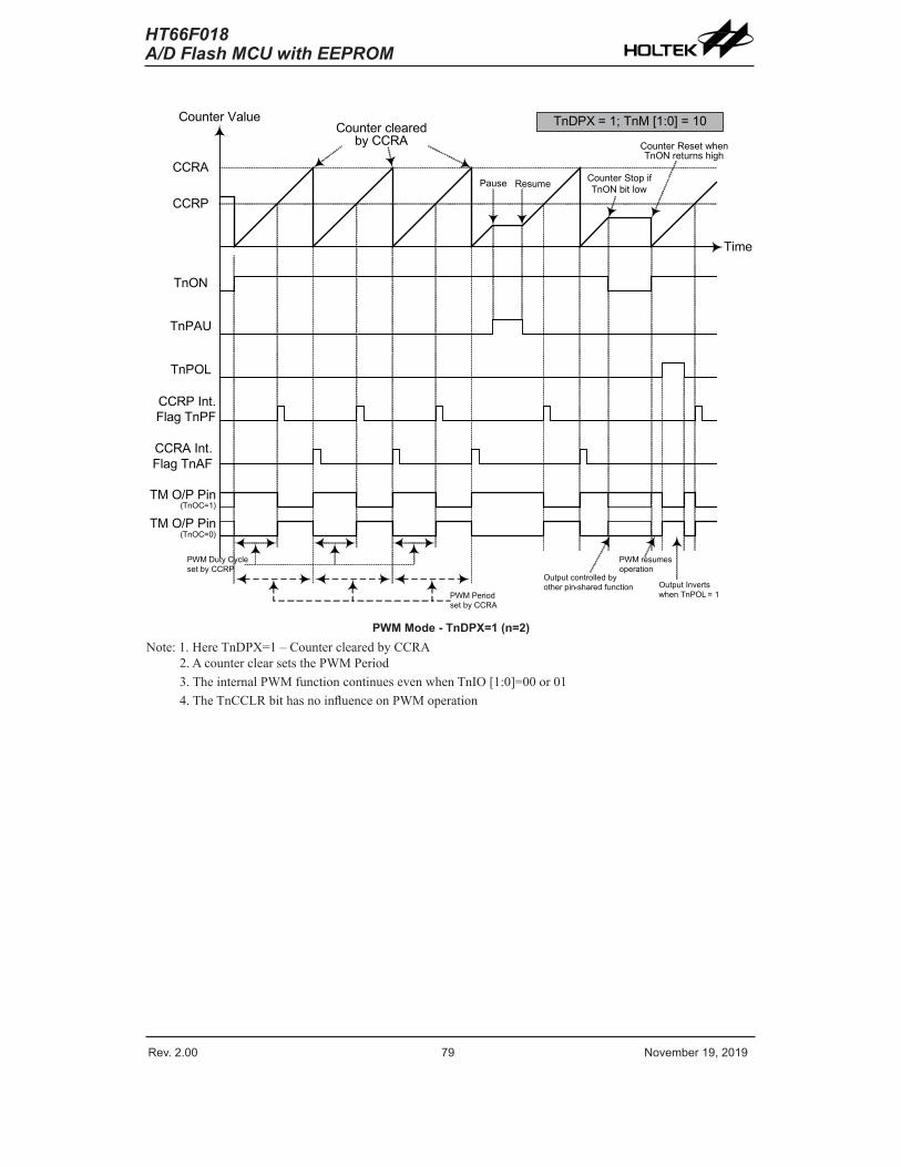
Rev. 2.00 78 November 19, 2019 Rev. 2.00 79 November 19, 2019
HT66F018A/D Flash MCU with EEPROM
HT66F018A/D Flash MCU with EEPROM
Counter Value
CCRP
CCRA
TnON
TnPAU
TnPOL
CCRP Int. Flag TnPF
CCRA Int. Flag TnAF
TM O/P Pin(TnOC=1)
Time
Counter cleared by CCRA
Pause Resume Counter Stop if TnON bit low
Counter Reset when TnON returns high
TnDPX = 1; TnM [1:0] = 10
PWM Duty Cycle set by CCRP
PWM resumes operation
Output controlled by other pin-shared function Output Inverts
when TnPOL = 1PWM Period set by CCRA
TM O/P Pin(TnOC=0)
PWM Mode - TnDPX=1 (n=2)Note: 1. Here TnDPX=1 – Counter cleared by CCRA
2. A counter clear sets the PWM Period3. The internal PWM function continues even when TnIO [1:0]=00 or 014. The TnCCLR bit has no influence on PWM operation
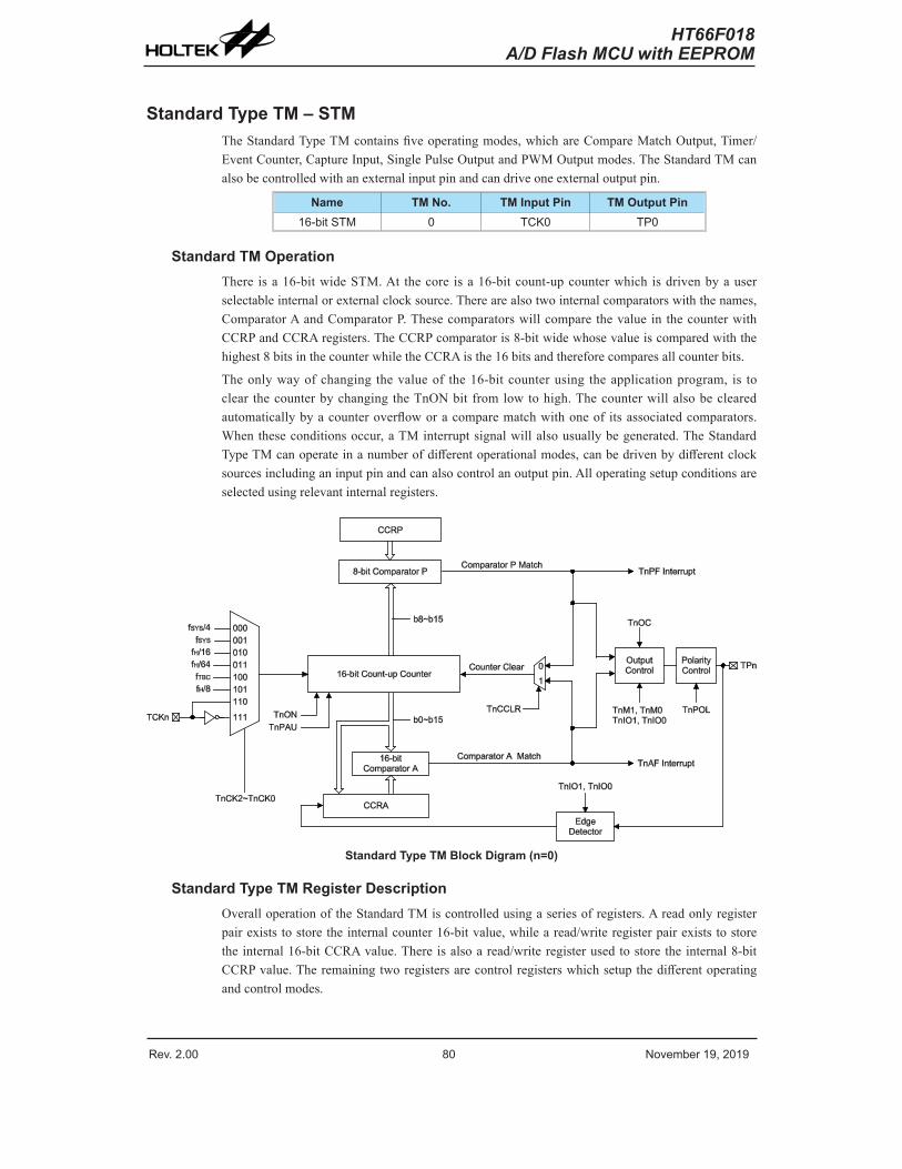
Rev. 2.00 80 November 19, 2019 Rev. 2.00 81 November 19, 2019
HT66F018A/D Flash MCU with EEPROM
HT66F018A/D Flash MCU with EEPROM
Standard Type TM – STMThe Standard Type TM contains five operating modes, which are Compare Match Output, Timer/Event Counter, Capture Input, Single Pulse Output and PWM Output modes. The Standard TM can also be controlled with an external input pin and can drive one external output pin.
Name TM No. TM Input Pin TM Output Pin16-bit STM 0 TCK0 TP0
Standard TM Operation There is a 16-bit wide STM. At the core is a 16-bit count-up counter which is driven by a user selectable internal or external clock source. There are also two internal comparators with the names, Comparator A and Comparator P. These comparators will compare the value in the counter with CCRP and CCRA registers. The CCRP comparator is 8-bit wide whose value is compared with the highest 8 bits in the counter while the CCRA is the 16 bits and therefore compares all counter bits.
The only way of changing the value of the 16-bit counter using the application program, is to clear the counter by changing the TnON bit from low to high. The counter will also be cleared automatically by a counter overflow or a compare match with one of its associated comparators. When these conditions occur, a TM interrupt signal will also usually be generated. The Standard Type TM can operate in a number of different operational modes, can be driven by different clock sources including an input pin and can also control an output pin. All operating setup conditions are selected using relevant internal registers.
Standard Type TM Block Digram (n=0)
Standard Type TM Register Description Overall operation of the Standard TM is controlled using a series of registers. A read only register pair exists to store the internal counter 16-bit value, while a read/write register pair exists to store the internal 16-bit CCRA value. There is also a read/write register used to store the internal 8-bit CCRP value. The remaining two registers are control registers which setup the different operating and control modes.
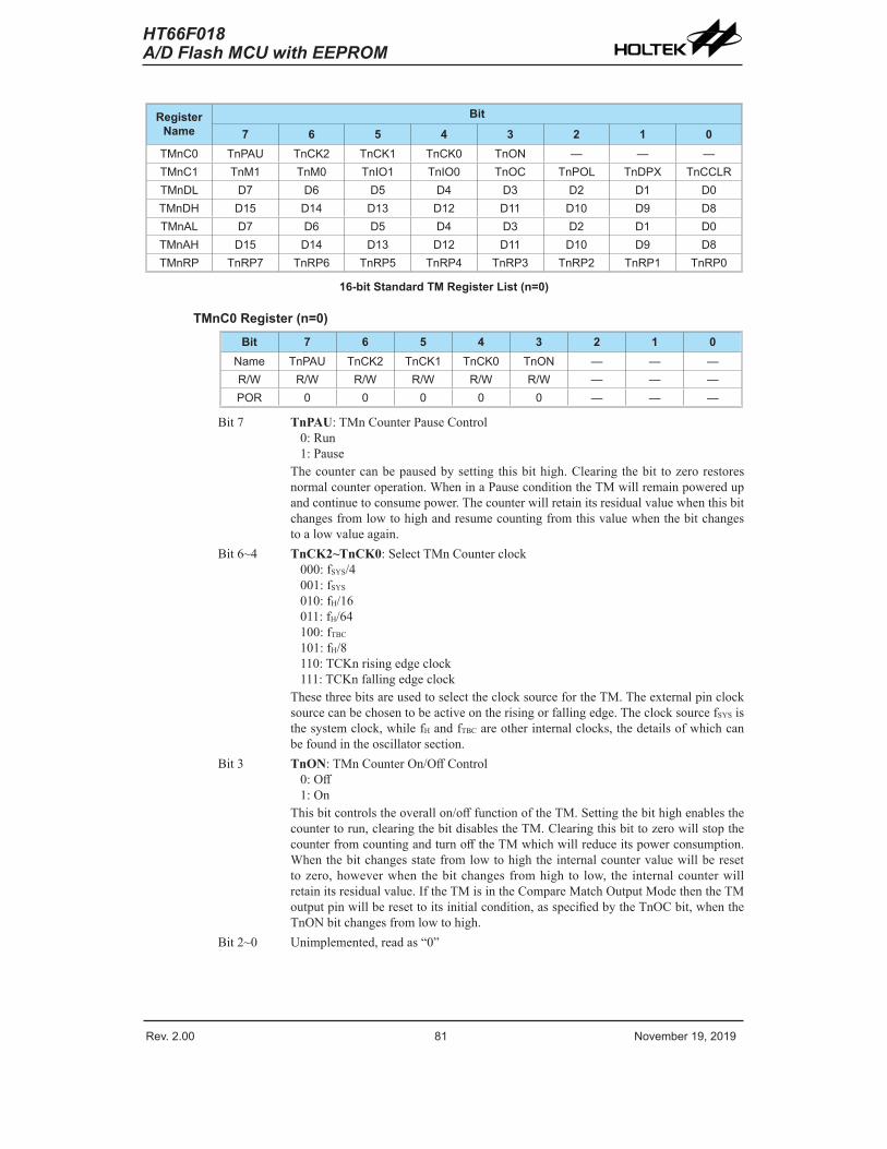
Rev. 2.00 80 November 19, 2019 Rev. 2.00 81 November 19, 2019
HT66F018A/D Flash MCU with EEPROM
HT66F018A/D Flash MCU with EEPROM
Register Name
Bit7 6 5 4 3 2 1 0
TMnC0 TnPAU TnCK2 TnCK1 TnCK0 TnON — — —TMnC1 TnM1 TnM0 TnIO1 TnIO0 TnOC TnPOL TnDPX TnCCLRTMnDL D7 D6 D5 D4 D3 D2 D1 D0TMnDH D15 D14 D13 D12 D11 D10 D9 D8TMnAL D7 D6 D5 D4 D3 D2 D1 D0TMnAH D15 D14 D13 D12 D11 D10 D9 D8TMnRP TnRP7 TnRP6 TnRP5 TnRP4 TnRP3 TnRP2 TnRP1 TnRP0
16-bit Standard TM Register List (n=0)
TMnC0 Register (n=0)Bit 7 6 5 4 3 2 1 0
Name TnPAU TnCK2 TnCK1 TnCK0 TnON — — —R/W R/W R/W R/W R/W R/W — — —POR 0 0 0 0 0 — — —
Bit 7 TnPAU: TMn Counter Pause Control0: Run1: Pause
The counter can be paused by setting this bit high. Clearing the bit to zero restores normal counter operation. When in a Pause condition the TM will remain powered up and continue to consume power. The counter will retain its residual value when this bit changes from low to high and resume counting from this value when the bit changes to a low value again.
Bit 6~4 TnCK2~TnCK0: Select TMn Counter clock000: fSYS/4001: fSYS
010: fH/16011: fH/64100: fTBC
101: fH/8110: TCKn rising edge clock111: TCKn falling edge clock
These three bits are used to select the clock source for the TM. The external pin clock source can be chosen to be active on the rising or falling edge. The clock source fSYS is the system clock, while fH and fTBC are other internal clocks, the details of which can be found in the oscillator section.
Bit 3 TnON: TMn Counter On/Off Control0: Off1: On
This bit controls the overall on/off function of the TM. Setting the bit high enables the counter to run, clearing the bit disables the TM. Clearing this bit to zero will stop the counter from counting and turn off the TM which will reduce its power consumption. When the bit changes state from low to high the internal counter value will be reset to zero, however when the bit changes from high to low, the internal counter will retain its residual value. If the TM is in the Compare Match Output Mode then the TM output pin will be reset to its initial condition, as specified by the TnOC bit, when the TnON bit changes from low to high.
Bit 2~0 Unimplemented, read as “0”
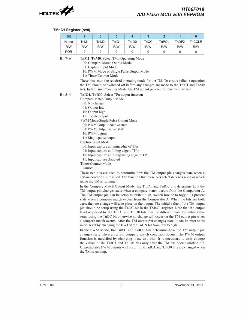
Rev. 2.00 82 November 19, 2019 Rev. 2.00 83 November 19, 2019
HT66F018A/D Flash MCU with EEPROM
HT66F018A/D Flash MCU with EEPROM
TMnC1 Register (n=0)Bit 7 6 5 4 3 2 1 0
Name TnM1 TnM0 TnIO1 TnIO0 TnOC TnPOL TnDPX TnCCLRR/W R/W R/W R/W R/W R/W R/W R/W R/WPOR 0 0 0 0 0 0 0 0
Bit 7~6 TnM1, TnM0: Select TMn Operating Mode00: Compare Match Output Mode01: Capture Input Mode10: PWM Mode or Single Pulse Output Mode11: Timer/Counter Mode
These bits setup the required operating mode for the TM. To ensure reliable operation the TM should be switched off before any changes are made to the TnM1 and TnM0 bits. In the Timer/Counter Mode, the TM output pin control must be disabled.
Bit 5~4 TnIO1, TnIO0: Select TPn output functionCompare Match Output Mode
00: No change01: Output low10: Output high11: Toggle output
PWM Mode/Single Pulse Output Mode00: PWM Output inactive state01: PWM Output active state10: PWM output11: Single pulse output
Capture Input Mode00: Input capture at rising edge of TPn01: Input capture at falling edge of TPn10: Input capture at falling/rising edge of TPn11: Input capture disabled
Timer/Counter Mode Unused
These two bits are used to determine how the TM output pin changes state when a certain condition is reached. The function that these bits select depends upon in which mode the TM is running.In the Compare Match Output Mode, the TnIO1 and TnIO0 bits determine how the TM output pin changes state when a compare match occurs from the Comparator A. The TM output pin can be setup to switch high, switch low or to toggle its present state when a compare match occurs from the Comparator A. When the bits are both zero, then no change will take place on the output. The initial value of the TM output pin should be setup using the TnOC bit in the TMnC1 register. Note that the output level requested by the TnIO1 and TnIO0 bits must be different from the initial value setup using the TnOC bit otherwise no change will occur on the TM output pin when a compare match occurs. After the TM output pin changes state, it can be reset to its initial level by changing the level of the TnON bit from low to high.In the PWM Mode, the TnIO1 and TnIO0 bits determine how the TM output pin changes state when a certain compare match condition occurs. The PWM output function is modified by changing these two bits. It is necessary to only change the values of the TnIO1 and TnIO0 bits only after the TM has been switched off. Unpredictable PWM outputs will occur if the TnIO1 and TnIO0 bits are changed when the TM is running.
Rev. 2.00 82 November 19, 2019 Rev. 2.00 83 November 19, 2019
HT66F018A/D Flash MCU with EEPROM
HT66F018A/D Flash MCU with EEPROM
Bit 3 TnOC: TPn Output control bitCompare Match Output Mode
0: Initial low1: Initial high
PWM Mode/Single Pulse Output Mode0: Active low1: Active high
This is the output control bit for the TM output pin. Its operation depends upon whether TM is being used in the Compare Match Output Mode or in the PWM Mode/Single Pulse Output Mode. It has no effect if the TM is in the Timer/Counter Mode. In the Compare Match Output Mode it determines the logic level of the TM output pin before a compare match occurs. In the PWM Mode it determines if the PWM signal is active high or active low.
Bit 2 TnPOL: TPn Output polarity Control0: Non-invert1: Invert
This bit controls the polarity of the TPn output pin. When the bit is set high the TM output pin will be inverted and not inverted when the bit is zero. It has no effect if the TM is in the Timer/Counter Mode.
Bit 1 TnDPX: TMn PWM period/duty Control0: CCRP - period; CCRA - duty1: CCRP - duty; CCRA - period
This bit, determines which of the CCRA and CCRP registers are used for period and duty control of the PWM waveform.
Bit 0 TnCCLR: Select TMn Counter clear condition0: TMn Comparatror P match1: TMn Comparatror A match
This bit is used to select the method which clears the counter. Remember that the Compact TM contains two comparators, Comparator A and Comparator P, either of which can be selected to clear the internal counter. With the TnCCLR bit set high, the counter will be cleared when a compare match occurs from the Comparator A. When the bit is low, the counter will be cleared when a compare match occurs from the Comparator P or with a counter overflow. A counter overflow clearing method can only be implemented if the CCRP bits are all cleared to zero. The TnCCLR bit is not used in the PWM Mode, Single Pulse or Input Capture Mode.
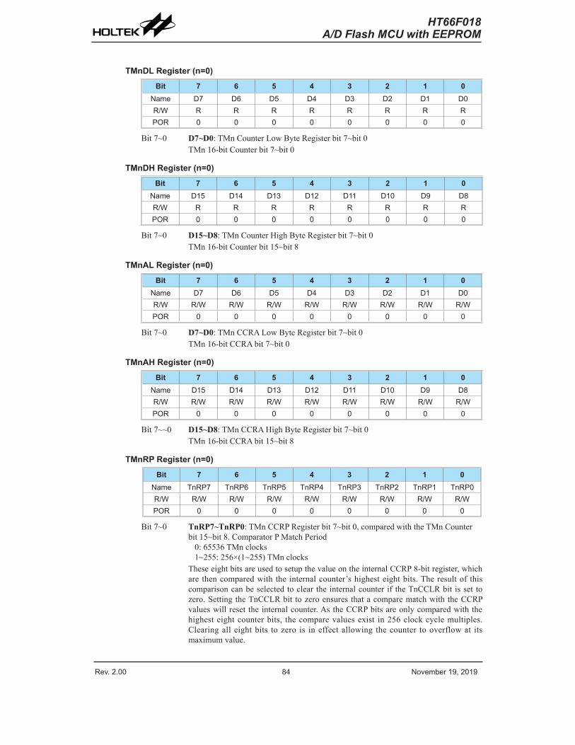
Rev. 2.00 84 November 19, 2019 Rev. 2.00 85 November 19, 2019
HT66F018A/D Flash MCU with EEPROM
HT66F018A/D Flash MCU with EEPROM
TMnDL Register (n=0)Bit 7 6 5 4 3 2 1 0
Name D7 D6 D5 D4 D3 D2 D1 D0R/W R R R R R R R RPOR 0 0 0 0 0 0 0 0
Bit 7~0 D7~D0: TMn Counter Low Byte Register bit 7~bit 0TMn 16-bit Counter bit 7~bit 0
TMnDH Register (n=0)Bit 7 6 5 4 3 2 1 0
Name D15 D14 D13 D12 D11 D10 D9 D8R/W R R R R R R R RPOR 0 0 0 0 0 0 0 0
Bit 7~0 D15~D8: TMn Counter High Byte Register bit 7~bit 0TMn 16-bit Counter bit 15~bit 8
TMnAL Register (n=0)Bit 7 6 5 4 3 2 1 0
Name D7 D6 D5 D4 D3 D2 D1 D0R/W R/W R/W R/W R/W R/W R/W R/W R/WPOR 0 0 0 0 0 0 0 0
Bit 7~0 D7~D0: TMn CCRA Low Byte Register bit 7~bit 0TMn 16-bit CCRA bit 7~bit 0
TMnAH Register (n=0)Bit 7 6 5 4 3 2 1 0
Name D15 D14 D13 D12 D11 D10 D9 D8R/W R/W R/W R/W R/W R/W R/W R/W R/WPOR 0 0 0 0 0 0 0 0
Bit 7~~0 D15~D8: TMn CCRA High Byte Register bit 7~bit 0TMn 16-bit CCRA bit 15~bit 8
TMnRP Register (n=0)Bit 7 6 5 4 3 2 1 0
Name TnRP7 TnRP6 TnRP5 TnRP4 TnRP3 TnRP2 TnRP1 TnRP0R/W R/W R/W R/W R/W R/W R/W R/W R/WPOR 0 0 0 0 0 0 0 0
Bit 7~0 TnRP7~TnRP0: TMn CCRP Register bit 7~bit 0, compared with the TMn Counter bit 15~bit 8. Comparator P Match Period
0: 65536 TMn clocks1~255: 256×(1~255) TMn clocks
These eight bits are used to setup the value on the internal CCRP 8-bit register, which are then compared with the internal counter’s highest eight bits. The result of this comparison can be selected to clear the internal counter if the TnCCLR bit is set to zero. Setting the TnCCLR bit to zero ensures that a compare match with the CCRP values will reset the internal counter. As the CCRP bits are only compared with the highest eight counter bits, the compare values exist in 256 clock cycle multiples. Clearing all eight bits to zero is in effect allowing the counter to overflow at its maximum value.
Rev. 2.00 84 November 19, 2019 Rev. 2.00 85 November 19, 2019
HT66F018A/D Flash MCU with EEPROM
HT66F018A/D Flash MCU with EEPROM
Standard Type TM Operating Modes The Standard Type TM can operate in one of five operating modes, Compare Match Output Mode, PWM Output Mode, Single Pulse Output Mode, Capture Input Mode or Timer/Counter Mode. The operating mode is selected using the TnM1 and TnM0 bits in the TMnC1 register.
Compare Output Mode To select this mode, bits TnM1 and TnM0 in the TMnC1 register, should be set to 00 respectively. In this mode once the counter is enabled and running it can be cleared by three methods. These are a counter overflow, a compare match from Comparator A and a compare match from Comparator P. When the TnCCLR bit is low, there are two ways in which the counter can be cleared. One is when a compare match from Comparator P, the other is when the CCRP bits are all zero which allows the counter to overflow. Here both TnAF and TnPF interrupt request flags for Comparator A and Comparator P respectively, will both be generated.
If the TnCCLR bit in the TMnC1 register is high then the counter will be cleared when a compare match occurs from Comparator A. However, here only the TnAF interrupt request flag will be generated even if the value of the CCRP bits is less than that of the CCRA registers. Therefore when TnCCLR is high no TnPF interrupt request flag will be generated. In the Compare Match Output Mode, the CCRA can not be set to “0”.
As the name of the mode suggests, after a comparison is made, the TM output pin, will change state. The TM output pin condition however only changes state when a TnAF interrupt request flag is generated after a compare match occurs from Comparator A. The TnPF interrupt request flag, generated from a compare match occurs from Comparator P, will have no effect on the TM output pin. The way in which the TM output pin changes state are determined by the condition of the TnIO1 and TnIO0 bits in the TMnC1 register. The TM output pin can be selected using the TnIO1 and TnIO0 bits to go high, to go low or to toggle from its present condition when a compare match occurs from Comparator A. The initial condition of the TM output pin, which is setup after the TnON bit changes from low to high, is setup using the TnOC bit. Note that if the TnIO1 and TnIO0 bits are zero then no pin change will take place.
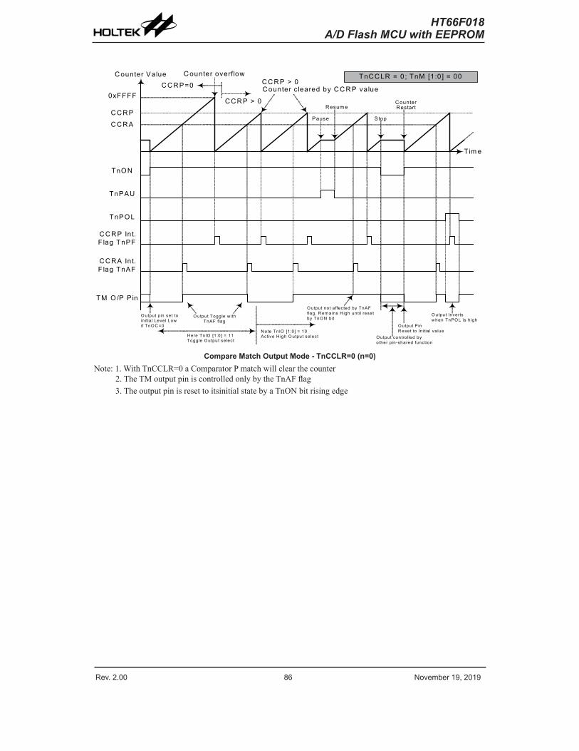
Rev. 2.00 86 November 19, 2019 Rev. 2.00 87 November 19, 2019
HT66F018A/D Flash MCU with EEPROM
HT66F018A/D Flash MCU with EEPROM
C ounter Value
C C R PC C R A
TnO N
TnPAU
TnPO L
C C R P Int. F lag TnPF
C C R A Int. F lag TnAF
TM O /P P in
T im e
C C R P=0
C C R P > 0
C ounter overflowC C R P > 0C ounter c leared by C C R P value
Pause
Resum e
Stop
Counter Restart
TnC C LR = 0 ; TnM [1:0] = 00
O utput p in set to in itia l Level Low if TnO C =0
O utput Toggle w ith TnAF flag
N ote TnIO [1 :0 ] = 10 Active H igh O utput se lectH ere TnIO [1 :0 ] = 11
Toggle O utput se lect
O utput not a ffected by TnAF flag. R em ains H igh until reset by TnO N bit
O utput P inR eset to In itia l va lue
O utput contro lled by other p in-shared function
O utput Invertsw hen TnPO L is h igh
0xFFFF
Compare Match Output Mode - TnCCLR=0 (n=0)Note: 1. With TnCCLR=0 a Comparator P match will clear the counter
2. The TM output pin is controlled only by the TnAF flag3. The output pin is reset to itsinitial state by a TnON bit rising edge
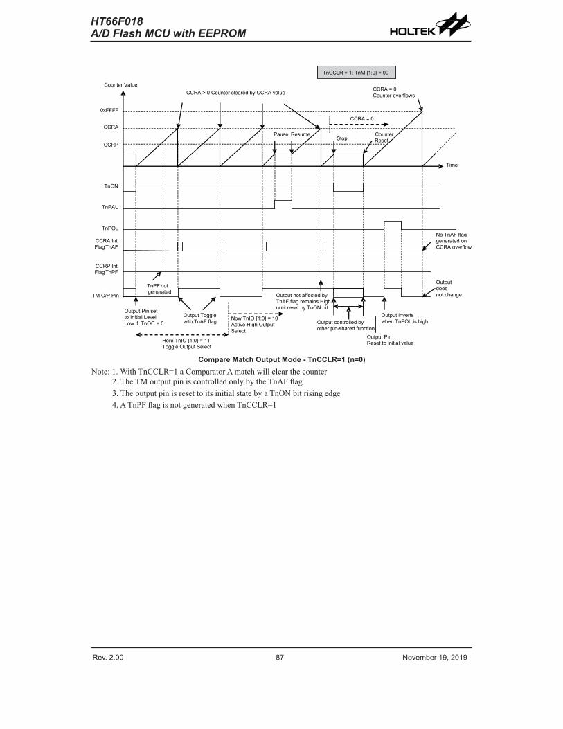
Rev. 2.00 86 November 19, 2019 Rev. 2.00 87 November 19, 2019
HT66F018A/D Flash MCU with EEPROM
HT66F018A/D Flash MCU with EEPROM
CCRP
CCRA
0xFFFF
CCRA = 0Counter overflows
CCRP Int.Flag TnPF
CCRA Int.Flag TnAF
CCRA > 0 Counter cleared by CCRA value
TM O/P Pin
TnON
Pause CounterReset
Output PinReset to initial value
Output Pin set to Initial LevelLow if TnOC = 0
Output Togglewith TnAF flag
Here TnIO [1:0] = 11Toggle Output Select
Now TnIO [1:0] = 10 Active High Output Select
TnPAU
ResumeStop
Time
TnPF notgenerated
No TnAF flaggenerated on CCRA overflow
Output doesnot change
CCRA = 0
Output invertswhen TnPOL is high
TnPOL
TnCCLR = 1; TnM [1:0] = 00
Output controlled byother pin-shared function
Output not affected byTnAF flag remains Highuntil reset by TnON bit
Counter Value
Compare Match Output Mode - TnCCLR=1 (n=0)Note: 1. With TnCCLR=1 a Comparator A match will clear the counter
2. The TM output pin is controlled only by the TnAF flag3. The output pin is reset to its initial state by a TnON bit rising edge4. A TnPF flag is not generated when TnCCLR=1
Rev. 2.00 88 November 19, 2019 Rev. 2.00 89 November 19, 2019
HT66F018A/D Flash MCU with EEPROM
HT66F018A/D Flash MCU with EEPROM
Timer/Counter Mode To select this mode, bits TnM1 and TnM0 in the TMnC1 register should be set to 11 respectively. The Timer/Counter Mode operates in an identical way to the Compare Match Output Mode generating the same interrupt flags. The exception is that in the Timer/Counter Mode the TM output pin is not used. Therefore the above description and Timing Diagrams for the Compare Match Output Mode can be used to understand its function. As the TM output pin is not used in this mode, the pin can be used as a normal I/O pin or other pin-shared function.
PWM Output Mode To select this mode, bits TnM1 and TnM0 in the TMnC1 register should be set to 10 respectively and also the TnIO1 and TnIO0 bits should be set to 10 respectively. The PWM function within the TM is useful for applications which require functions such as motor control, heating control, illumination control etc. By providing a signal of fixed frequency but of varying duty cycle on the TM output pin, a square wave AC waveform can be generated with varying equivalent DC RMS values.
As both the period and duty cycle of the PWM waveform can be controlled, the choice of generated waveform is extremely flexible. In the PWM mode, the TnCCLR bit has no effect as the PWM period. Both of the CCRA and CCRP registers are used to generate the PWM waveform, one register is used to clear the internal counter and thus control the PWM waveform frequency, while the other one is used to control the duty cycle. Which register is used to control either frequency or duty cycle is determined using the TnDPX bit in the TMnC1 register. The PWM waveform frequency and duty cycle can therefore be controlled by the values in the CCRA and CCRP registers.
An interrupt flag, one for each of the CCRA and CCRP, will be generated when a compare match occurs from either Comparator A or Comparator P. The TnOC bit in the TMnC1 register is used to select the required polarity of the PWM waveform while the two TnIO1 and TnIO0 bits are used to enable the PWM output or to force the TM output pin to a fixed high or low level. The TnPOL bit is used to reverse the polarity of the PWM output waveform.
16-bit STM, PWM Mode, Edge-aligned Mode, TnDPX=0CCRP 1~255 0Period CCRP×256 65536Duty CCRA
If fSYS=16MHz, TM clock source select fSYS/4, CCRP=2 and CCRA=128,
The STM PWM output frequency=(fSYS/4)/(2×256)=fSYS/2048=7.8125kHz, duty=128/(2×256)=25%.
If the Duty value defined by the CCRA register is equal to or greater than the Period value, then the PWM output duty is 100%.
16-bit STM, PWM Mode, Edge-aligned Mode, TnDPX=1CCRP 1~255 0Period CCRADuty CCRP×256 65536
The PWM output period is determined by the CCRA register value together with the TM clock while the PWM duty cycle is defined by the (CCRP×256) except when the CCRP value is equal to 000b.

Rev. 2.00 88 November 19, 2019 Rev. 2.00 89 November 19, 2019
HT66F018A/D Flash MCU with EEPROM
HT66F018A/D Flash MCU with EEPROM
Counter Value
CCRP
CCRA
TnON
TnPAU
TnPOL
CCRP Int. Flag TnPF
CCRA Int. Flag TnAF
TM O/P Pin(TnOC=1)
Time
Counter cleared by CCRP
Pause Resume Counter Stop if TnON bit low
Counter Reset when TnON returns high
TnDPX = 0; TnM [1:0] = 10
PWM Duty Cycle set by CCRA
PWM resumes operation
Output controlled by other pin-shared function Output Inverts
when TnPOL = 1PWM Period set by CCRP
TM O/P Pin(TnOC=0)
PWM Mode - TnDPX=0 (n=0)Note: 1. Here TnDPX=0 – Counter cleared by CCRP
2. A counter clear sets the PWM Period3. The internal PWM function continues running even when TnIO [1:0]=00 or 014. The TnCCLR bit has no influence on PWM operation
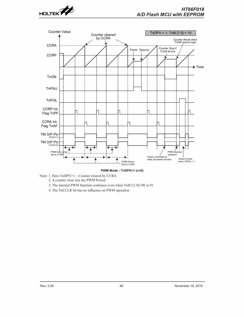
Rev. 2.00 90 November 19, 2019 Rev. 2.00 91 November 19, 2019
HT66F018A/D Flash MCU with EEPROM
HT66F018A/D Flash MCU with EEPROM
Counter Value
CCRP
CCRA
TnON
TnPAU
TnPOL
CCRP Int. Flag TnPF
CCRA Int. Flag TnAF
TM O/P Pin(TnOC=1)
Time
Counter cleared by CCRA
Pause Resume Counter Stop if TnON bit low
Counter Reset when TnON returns high
TnDPX = 1; TnM [1:0] = 10
PWM Duty Cycle set by CCRP
PWM resumes operation
Output controlled by other pin-shared function Output Inverts
when TnPOL = 1PWM Period set by CCRA
TM O/P Pin(TnOC=0)
PWM Mode - TnDPX=1 (n=0)Note: 1. Here TnDPX=1 – Counter cleared by CCRA
2. A counter clear sets the PWM Period3. The internal PWM function continues even when TnIO [1:0]=00 or 014. The TnCCLR bit has no influence on PWM operation
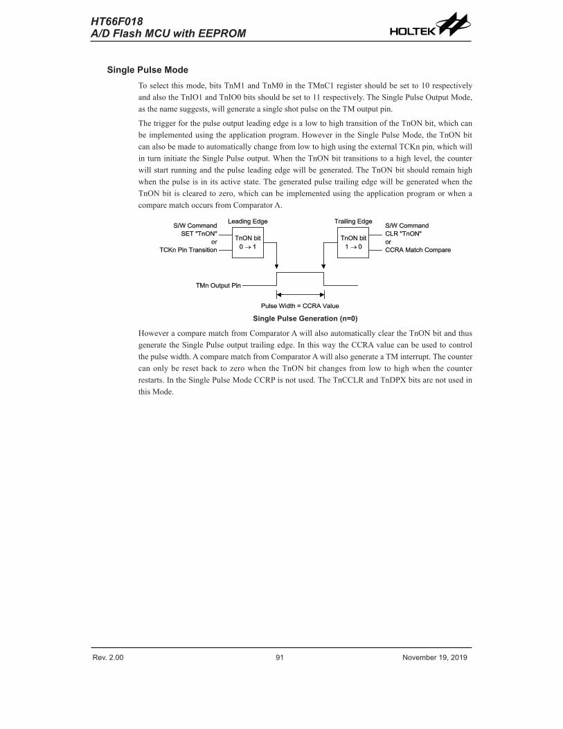
Rev. 2.00 90 November 19, 2019 Rev. 2.00 91 November 19, 2019
HT66F018A/D Flash MCU with EEPROM
HT66F018A/D Flash MCU with EEPROM
Single Pulse Mode To select this mode, bits TnM1 and TnM0 in the TMnC1 register should be set to 10 respectively and also the TnIO1 and TnIO0 bits should be set to 11 respectively. The Single Pulse Output Mode, as the name suggests, will generate a single shot pulse on the TM output pin.
The trigger for the pulse output leading edge is a low to high transition of the TnON bit, which can be implemented using the application program. However in the Single Pulse Mode, the TnON bit can also be made to automatically change from low to high using the external TCKn pin, which will in turn initiate the Single Pulse output. When the TnON bit transitions to a high level, the counter will start running and the pulse leading edge will be generated. The TnON bit should remain high when the pulse is in its active state. The generated pulse trailing edge will be generated when the TnON bit is cleared to zero, which can be implemented using the application program or when a compare match occurs from Comparator A.
Single Pulse Generation (n=0)
However a compare match from Comparator A will also automatically clear the TnON bit and thus generate the Single Pulse output trailing edge. In this way the CCRA value can be used to control the pulse width. A compare match from Comparator A will also generate a TM interrupt. The counter can only be reset back to zero when the TnON bit changes from low to high when the counter restarts. In the Single Pulse Mode CCRP is not used. The TnCCLR and TnDPX bits are not used in this Mode.
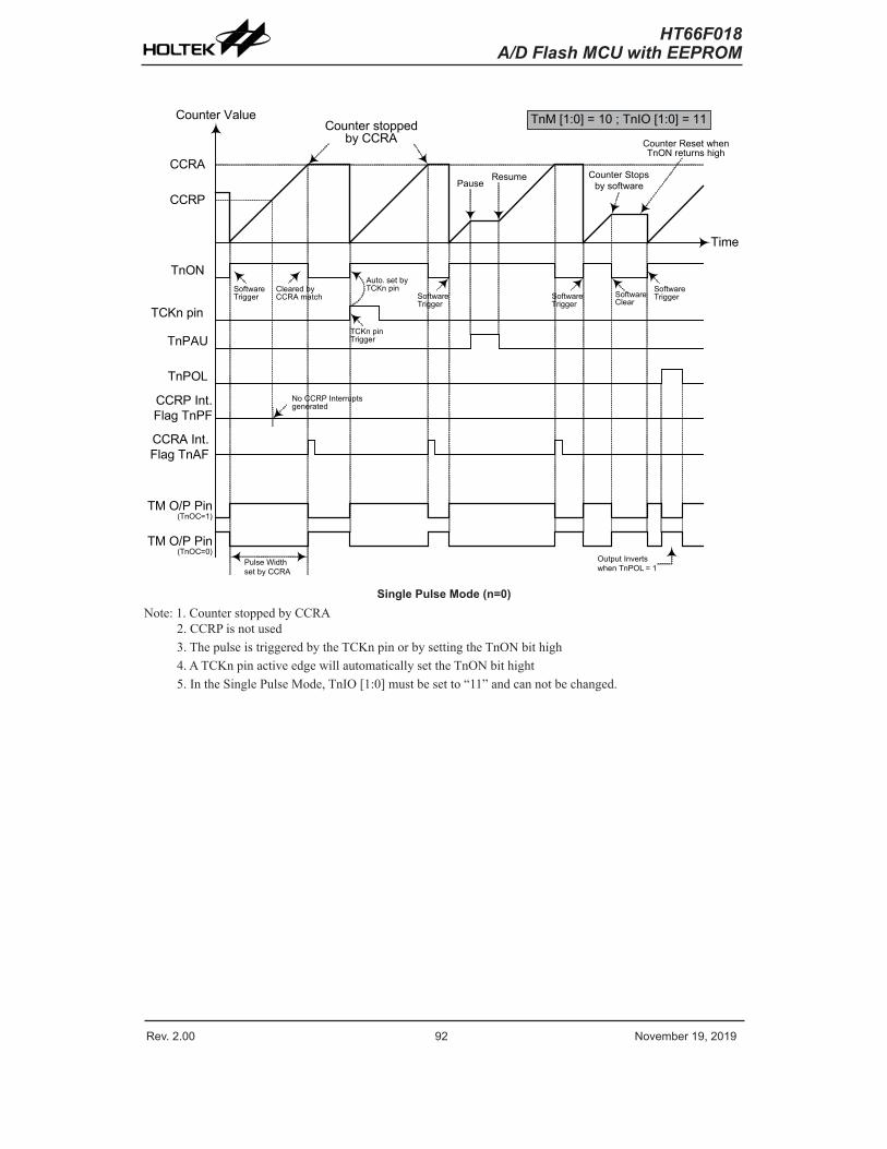
Rev. 2.00 92 November 19, 2019 Rev. 2.00 93 November 19, 2019
HT66F018A/D Flash MCU with EEPROM
HT66F018A/D Flash MCU with EEPROM
Counter Value
CCRP
CCRA
TnON
TnPAU
TnPOL
CCRP Int. Flag TnPF
CCRA Int. Flag TnAF
TM O/P Pin(TnOC=1)
Time
Counter stopped by CCRA
PauseResume Counter Stops
by software
Counter Reset when TnON returns high
TnM [1:0] = 10 ; TnIO [1:0] = 11
Pulse Width set by CCRA
Output Invertswhen TnPOL = 1
No CCRP Interrupts generated
TM O/P Pin(TnOC=0)
TCKn pin
Software Trigger
Cleared by CCRA match
TCKn pin Trigger
Auto. set by TCKn pin
Software Trigger
Software Clear
Software TriggerSoftware
Trigger
Single Pulse Mode (n=0)Note: 1. Counter stopped by CCRA
2. CCRP is not used3. The pulse is triggered by the TCKn pin or by setting the TnON bit high4. A TCKn pin active edge will automatically set the TnON bit hight 5. In the Single Pulse Mode, TnIO [1:0] must be set to “11” and can not be changed.
Rev. 2.00 92 November 19, 2019 Rev. 2.00 93 November 19, 2019
HT66F018A/D Flash MCU with EEPROM
HT66F018A/D Flash MCU with EEPROM
Capture Input Mode To select this mode bits TnM1 and TnM0 in the TMnC1 register should be set to 01 respectively. This mode enables external signals to capture and store the present value of the internal counter and can therefore be used for applications such as pulse width measurements. The external signal is supplied on the TPn pin, whose active edge can be either a rising edge, a falling edge or both rising and falling edges; the active edge transition type is selected using the TnIO1 and TnIO0 bits in the TMnC1 register. The counter is started when the TnON bit changes from low to high which is initiated using the application program.
When the required edge transition appears on the TPn pin the present value in the counter will be latched into the CCRA registers and a TM interrupt generated. Irrespective of what events occur on the TPn pin the counter will continue to free run until the TnON bit changes from high to low. When a CCRP compare match occurs the counter will reset back to zero; in this way the CCRP value can be used to control the maximum counter value. When a CCRP compare match occurs from Comparator P, a TM interrupt will also be generated. Counting the number of overflow interrupt signals from the CCRP can be a useful method in measuring long pulse widths. The TnIO1 and TnIO0 bits can select the active trigger edge on the TPn pin to be a rising edge, falling edge or both edge types. If the TnIO1 and TnIO0 bits are both set high, then no capture operation will take place irrespective of what happens on the TPn pin, however it must be noted that the counter will continue to run.
As the TPn pin is pin shared with other functions, care must be taken if the TM is in the Input Capture Mode. This is because if the pin is setup as an output, then any transitions on this pin may cause an input capture operation to be executed. The TnCCLR and TnDPX bits are not used in this Mode.
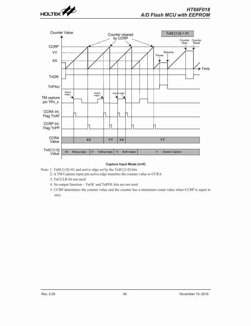
Rev. 2.00 94 November 19, 2019 Rev. 2.00 95 November 19, 2019
HT66F018A/D Flash MCU with EEPROM
HT66F018A/D Flash MCU with EEPROM
Counter Value
YYCCRP
TnON
TnPAU
CCRP Int. Flag TnPF
CCRA Int. Flag TnAF
CCRA Value
Time
Counter cleared by CCRP
PauseResume
Counter Reset
TnM [1:0] = 01
TM capture pin TPn_x
XX
Counter Stop
TnIO [1:0] Value
XX YY XX YY
Active edge Active
edgeActive edge
00 – Rising edge 01 – Falling edge 10 – Both edges 11 – Disable Capture
Capture Input Mode (n=0)Note: 1. TnM [1:0]=01 and active edge set by the TnIO [1:0] bits
2. A TM Capture input pin active edge transfers the counter value to CCRA3. TnCCLR bit not used4. No output function – TnOC and TnPOL bits are not used 5. CCRP determines the counter value and the counter has a maximum count value when CCRP is equal to
zero.

Rev. 2.00 94 November 19, 2019 Rev. 2.00 95 November 19, 2019
HT66F018A/D Flash MCU with EEPROM
HT66F018A/D Flash MCU with EEPROM
Periodic Type TM – PTMThe Periodic Type TM contains five operating modes, which are Compare Match Output, Timer/Event Counter, Capture Input, Single Pulse Output and PWM Output modes. The Periodic TM can also be controlled with an external input pin and can drive one external output pin.
Name TM No. TM Input Pin TM Output Pin10-bit PTM 1 TCK1 TP1
Periodic TM OperationAt its core is a 10-bit count-up counter which is driven by a user selectable internal or external clock source. There are two internal comparators with the names, Comparator A and Comparator P. These comparators will compare the value in the counter with the CCRA and CCRP registers.
The only way of changing the value of the 10-bit counter using the application program, is to clear the counter by changing the TnON bit from low to high. The counter will also be cleared automatically by a counter overflow or a compare match with one of its associated comparators. When these conditions occur, a TM interrupt signal will also usually be generated. The Periodic Type TM can operate in a number of different operational modes, can be driven by different clock sources including an input pin and can also control the output pin. All operating setup conditions are selected using relevant internal registers.
� � � �
� � � �
� � � � � �
� � � � � � � � � � � � � � � � � �
� � � � � � � � � � � � � � � � � � �
� � � � � � � � � �
� �
� � � � �
� � � � �
� � � � � � � � � � � � � � � � � � � �
� � � � � � �� � � � � � � � � � � �
� � � � � � � � � � � � �� � � � � � � � � � � � � � � � � � � � � � �
� � � � � � � � � � � � � �
� � � � � � � � � � � � � �
� � � � � � �� � � � � � � � � � �
� � � � �
� � � � � � � � � �
� � � � � � � � � �
� � � � � � � � � �� � � � � � � � � �
� � � �
� � �
� � � � � � � �� � � � � � �
� � � � �� � � � � � �
� � �
� � � � � � �
� � �� � �� � �� � �� � �� � �� � �
� � � � � �� � � �� � � � �� � � � �� � � �� �
��
��
� � � � � � �
� � �
Periodic Type TM Block Diagram (n=1)
Periodic Type TM Register DescriptionOverall operation of the Periodic TM is controlled using a series of registers. A read only register pair exists to store the internal counter 10-bit value, while two read/write register pairs exist to store the internal 10-bit CCRA and CCRP value. The remaining two registers are control registers which setup the different operating and control modes.
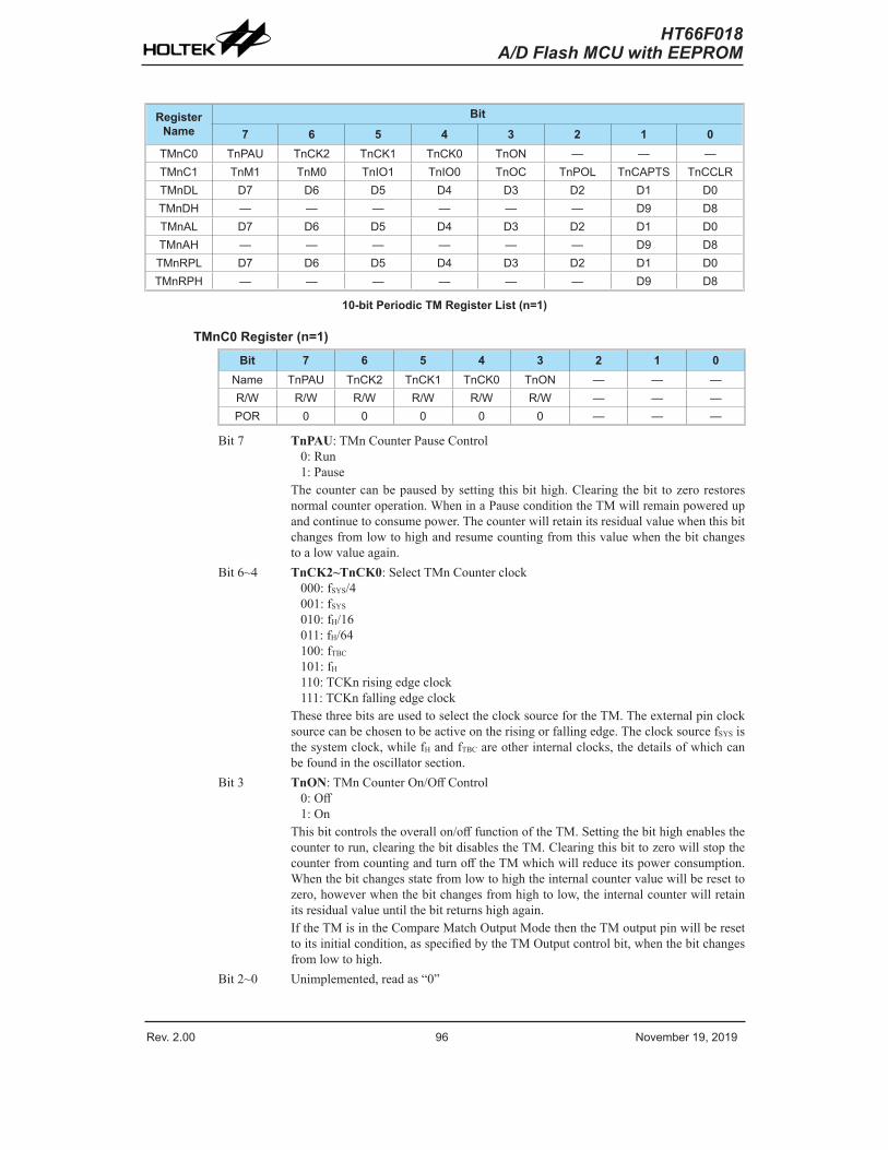
Rev. 2.00 96 November 19, 2019 Rev. 2.00 97 November 19, 2019
HT66F018A/D Flash MCU with EEPROM
HT66F018A/D Flash MCU with EEPROM
Register Name
Bit7 6 5 4 3 2 1 0
TMnC0 TnPAU TnCK2 TnCK1 TnCK0 TnON — — —TMnC1 TnM1 TnM0 TnIO1 TnIO0 TnOC TnPOL TnCAPTS TnCCLRTMnDL D7 D6 D5 D4 D3 D2 D1 D0TMnDH — — — — — — D9 D8TMnAL D7 D6 D5 D4 D3 D2 D1 D0TMnAH — — — — — — D9 D8TMnRPL D7 D6 D5 D4 D3 D2 D1 D0TMnRPH — — — — — — D9 D8
10-bit Periodic TM Register List (n=1)
TMnC0 Register (n=1)Bit 7 6 5 4 3 2 1 0
Name TnPAU TnCK2 TnCK1 TnCK0 TnON — — —R/W R/W R/W R/W R/W R/W — — —POR 0 0 0 0 0 — — —
Bit 7 TnPAU: TMn Counter Pause Control0: Run1: Pause
The counter can be paused by setting this bit high. Clearing the bit to zero restores normal counter operation. When in a Pause condition the TM will remain powered up and continue to consume power. The counter will retain its residual value when this bit changes from low to high and resume counting from this value when the bit changes to a low value again.
Bit 6~4 TnCK2~TnCK0: Select TMn Counter clock000: fSYS/4001: fSYS
010: fH/16011: fH/64100: fTBC
101: fH
110: TCKn rising edge clock111: TCKn falling edge clock
These three bits are used to select the clock source for the TM. The external pin clock source can be chosen to be active on the rising or falling edge. The clock source fSYS is the system clock, while fH and fTBC are other internal clocks, the details of which can be found in the oscillator section.
Bit 3 TnON: TMn Counter On/Off Control0: Off1: On
This bit controls the overall on/off function of the TM. Setting the bit high enables the counter to run, clearing the bit disables the TM. Clearing this bit to zero will stop the counter from counting and turn off the TM which will reduce its power consumption. When the bit changes state from low to high the internal counter value will be reset to zero, however when the bit changes from high to low, the internal counter will retain its residual value until the bit returns high again. If the TM is in the Compare Match Output Mode then the TM output pin will be reset to its initial condition, as specified by the TM Output control bit, when the bit changes from low to high.
Bit 2~0 Unimplemented, read as “0”
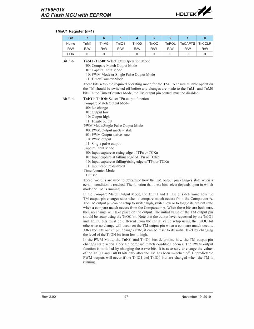
Rev. 2.00 96 November 19, 2019 Rev. 2.00 97 November 19, 2019
HT66F018A/D Flash MCU with EEPROM
HT66F018A/D Flash MCU with EEPROM
TMnC1 Register (n=1)Bit 7 6 5 4 3 2 1 0
Name TnM1 TnM0 TnIO1 TnIO0 TnOC TnPOL TnCAPTS TnCCLRR/W R/W R/W R/W R/W R/W R/W R/W R/WPOR 0 0 0 0 0 0 0 0
Bit 7~6 TnM1~TnM0: Select TMn Operation Mode00: Compare Match Output Mode01: Capture Input Mode10: PWM Mode or Single Pulse Output Mode11: Timer/Counter Mode
These bits setup the required operating mode for the TM. To ensure reliable operation the TM should be switched off before any changes are made to the TnM1 and TnM0 bits. In the Timer/Counter Mode, the TM output pin control must be disabled.
Bit 5~4 TnIO1~TnIO0: Select TPn output function Compare Match Output Mode
00: No change01: Output low10: Output high11: Toggle output
PWM Mode/Single Pulse Output Mode00: PWM Output inactive state01: PWM Output active state10: PWM output11: Single pulse output
Capture Input Mode00: Input capture at rising edge of TPn or TCKn01: Input capture at falling edge of TPn or TCKn10: Input capture at falling/rising edge of TPn or TCKn11: Input capture disabled
Timer/counter ModeUnused
These two bits are used to determine how the TM output pin changes state when a certain condition is reached. The function that these bits select depends upon in which mode the TM is running. In the Compare Match Output Mode, the TnIO1 and TnIO0 bits determine how the TM output pin changes state when a compare match occurs from the Comparator A. The TM output pin can be setup to switch high, switch low or to toggle its present state when a compare match occurs from the Comparator A. When these bits are both zero, then no change will take place on the output. The initial value of the TM output pin should be setup using the TnOC bit. Note that the output level requested by the TnIO1 and TnIO0 bits must be different from the initial value setup using the TnOC bit otherwise no change will occur on the TM output pin when a compare match occurs. After the TM output pin changes state, it can be reset to its initial level by changing the level of the TnON bit from low to high.In the PWM Mode, the TnIO1 and TnIO0 bits determine how the TM output pin changes state when a certain compare match condition occurs. The PWM output function is modified by changing these two bits. It is necessary to change the values of the TnIO1 and TnIO0 bits only after the TM has been switched off. Unpredictable PWM outputs will occur if the TnIO1 and TnIO0 bits are changed when the TM is running.
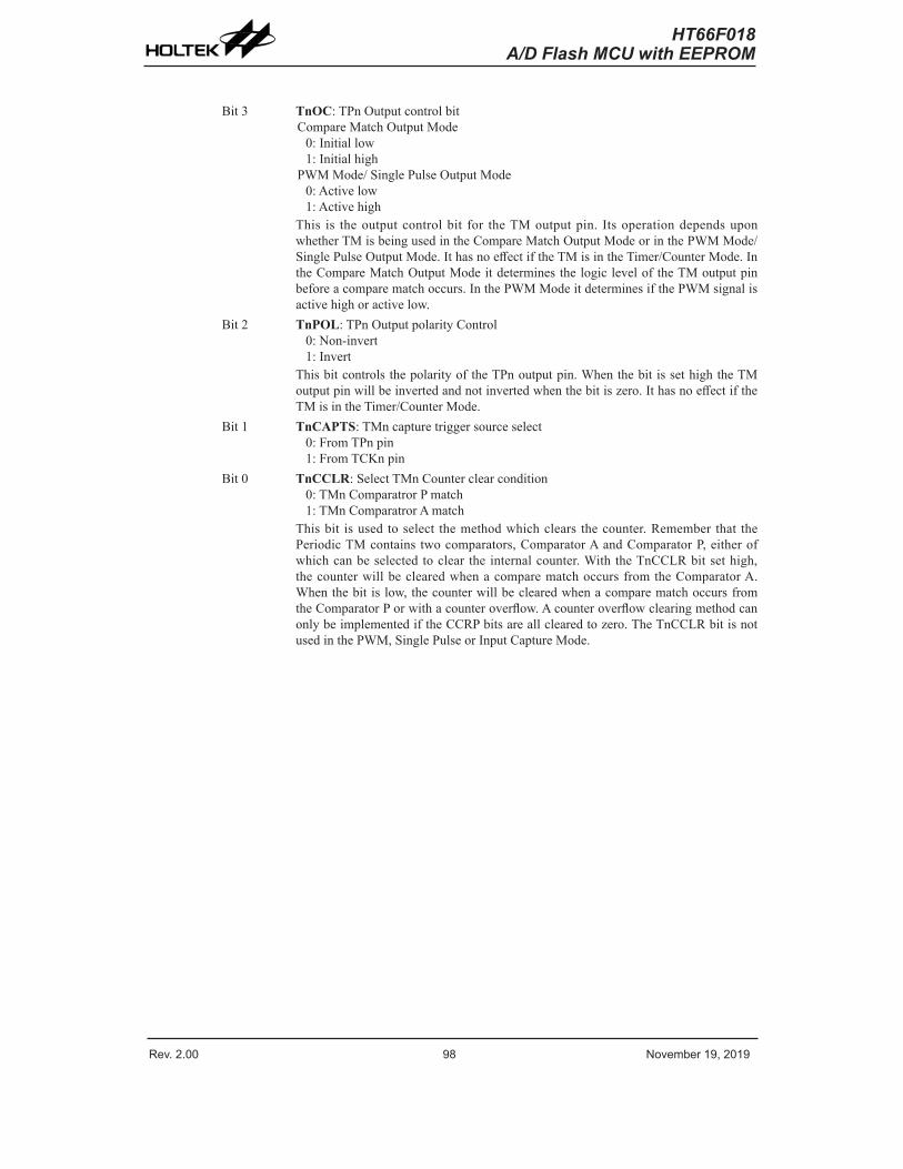
Rev. 2.00 98 November 19, 2019 Rev. 2.00 99 November 19, 2019
HT66F018A/D Flash MCU with EEPROM
HT66F018A/D Flash MCU with EEPROM
Bit 3 TnOC: TPn Output control bitCompare Match Output Mode
0: Initial low1: Initial high
PWM Mode/ Single Pulse Output Mode0: Active low1: Active high
This is the output control bit for the TM output pin. Its operation depends upon whether TM is being used in the Compare Match Output Mode or in the PWM Mode/Single Pulse Output Mode. It has no effect if the TM is in the Timer/Counter Mode. In the Compare Match Output Mode it determines the logic level of the TM output pin before a compare match occurs. In the PWM Mode it determines if the PWM signal is active high or active low.
Bit 2 TnPOL: TPn Output polarity Control0: Non-invert1: Invert
This bit controls the polarity of the TPn output pin. When the bit is set high the TM output pin will be inverted and not inverted when the bit is zero. It has no effect if the TM is in the Timer/Counter Mode.
Bit 1 TnCAPTS: TMn capture trigger source select0: From TPn pin1: From TCKn pin
Bit 0 TnCCLR: Select TMn Counter clear condition 0: TMn Comparatror P match 1: TMn Comparatror A match
This bit is used to select the method which clears the counter. Remember that the Periodic TM contains two comparators, Comparator A and Comparator P, either of which can be selected to clear the internal counter. With the TnCCLR bit set high, the counter will be cleared when a compare match occurs from the Comparator A. When the bit is low, the counter will be cleared when a compare match occurs from the Comparator P or with a counter overflow. A counter overflow clearing method can only be implemented if the CCRP bits are all cleared to zero. The TnCCLR bit is not used in the PWM, Single Pulse or Input Capture Mode.
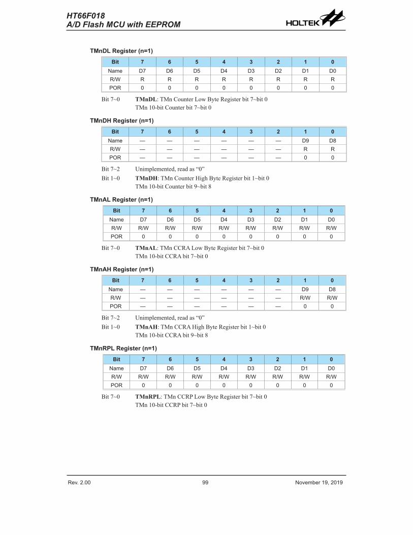
Rev. 2.00 98 November 19, 2019 Rev. 2.00 99 November 19, 2019
HT66F018A/D Flash MCU with EEPROM
HT66F018A/D Flash MCU with EEPROM
TMnDL Register (n=1)Bit 7 6 5 4 3 2 1 0
Name D7 D6 D5 D4 D3 D2 D1 D0R/W R R R R R R R RPOR 0 0 0 0 0 0 0 0
Bit 7~0 TMnDL: TMn Counter Low Byte Register bit 7~bit 0TMn 10-bit Counter bit 7~bit 0
TMnDH Register (n=1)Bit 7 6 5 4 3 2 1 0
Name — — — — — — D9 D8R/W — — — — — — R RPOR — — — — — — 0 0
Bit 7~2 Unimplemented, read as “0”Bit 1~0 TMnDH: TMn Counter High Byte Register bit 1~bit 0
TMn 10-bit Counter bit 9~bit 8
TMnAL Register (n=1)Bit 7 6 5 4 3 2 1 0
Name D7 D6 D5 D4 D3 D2 D1 D0R/W R/W R/W R/W R/W R/W R/W R/W R/WPOR 0 0 0 0 0 0 0 0
Bit 7~0 TMnAL: TMn CCRA Low Byte Register bit 7~bit 0TMn 10-bit CCRA bit 7~bit 0
TMnAH Register (n=1)Bit 7 6 5 4 3 2 1 0
Name — — — — — — D9 D8R/W — — — — — — R/W R/WPOR — — — — — — 0 0
Bit 7~2 Unimplemented, read as “0”Bit 1~0 TMnAH: TMn CCRA High Byte Register bit 1~bit 0
TMn 10-bit CCRA bit 9~bit 8
TMnRPL Register (n=1)Bit 7 6 5 4 3 2 1 0
Name D7 D6 D5 D4 D3 D2 D1 D0R/W R/W R/W R/W R/W R/W R/W R/W R/WPOR 0 0 0 0 0 0 0 0
Bit 7~0 TMnRPL: TMn CCRP Low Byte Register bit 7~bit 0TMn 10-bit CCRP bit 7~bit 0
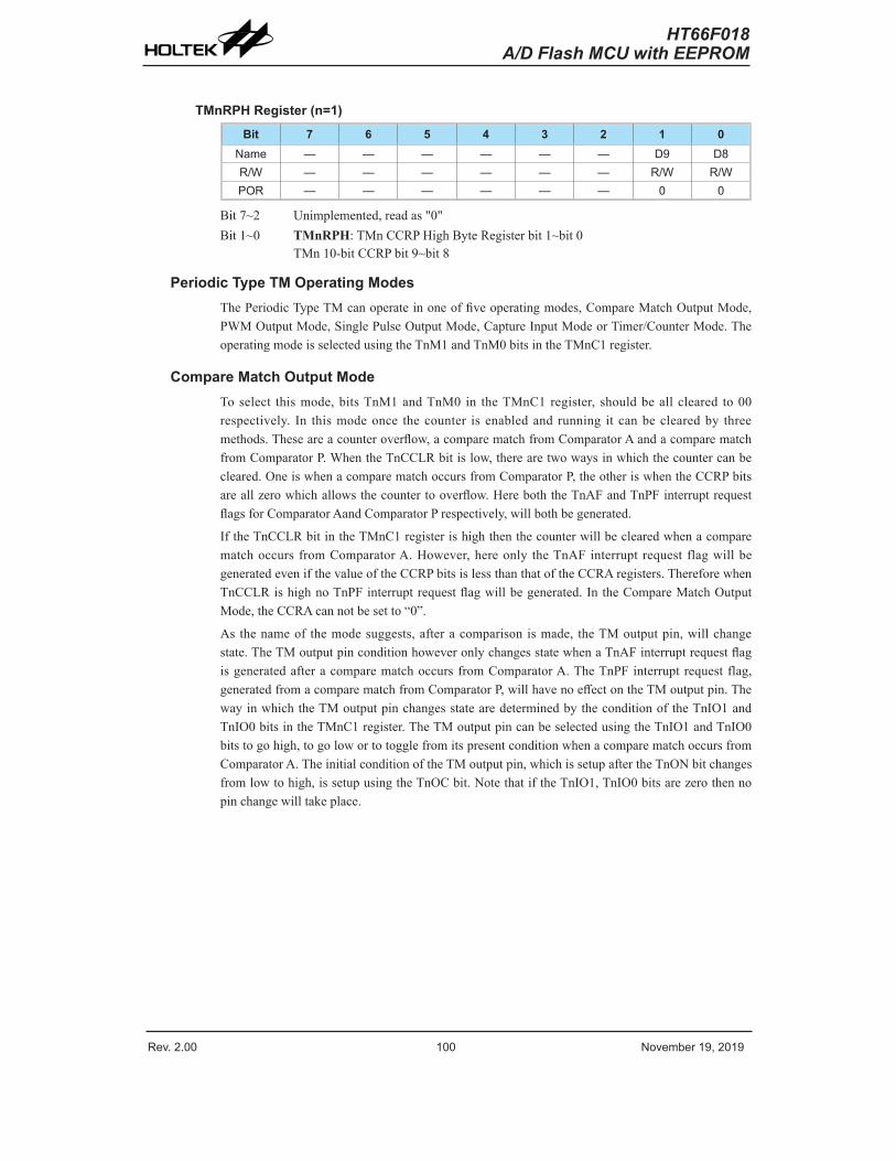
Rev. 2.00 100 November 19, 2019 Rev. 2.00 101 November 19, 2019
HT66F018A/D Flash MCU with EEPROM
HT66F018A/D Flash MCU with EEPROM
TMnRPH Register (n=1)Bit 7 6 5 4 3 2 1 0
Name — — — — — — D9 D8R/W — — — — — — R/W R/WPOR — — — — — — 0 0
Bit 7~2 Unimplemented, read as "0"Bit 1~0 TMnRPH: TMn CCRP High Byte Register bit 1~bit 0
TMn 10-bit CCRP bit 9~bit 8
Periodic Type TM Operating ModesThe Periodic Type TM can operate in one of five operating modes, Compare Match Output Mode, PWM Output Mode, Single Pulse Output Mode, Capture Input Mode or Timer/Counter Mode. The operating mode is selected using the TnM1 and TnM0 bits in the TMnC1 register.
Compare Match Output ModeTo select this mode, bits TnM1 and TnM0 in the TMnC1 register, should be all cleared to 00 respectively. In this mode once the counter is enabled and running it can be cleared by three methods. These are a counter overflow, a compare match from Comparator A and a compare match from Comparator P. When the TnCCLR bit is low, there are two ways in which the counter can be cleared. One is when a compare match occurs from Comparator P, the other is when the CCRP bits are all zero which allows the counter to overflow. Here both the TnAF and TnPF interrupt request flags for Comparator Aand Comparator P respectively, will both be generated.
If the TnCCLR bit in the TMnC1 register is high then the counter will be cleared when a compare match occurs from Comparator A. However, here only the TnAF interrupt request flag will be generated even if the value of the CCRP bits is less than that of the CCRA registers. Therefore when TnCCLR is high no TnPF interrupt request flag will be generated. In the Compare Match Output Mode, the CCRA can not be set to “0”.
As the name of the mode suggests, after a comparison is made, the TM output pin, will change state. The TM output pin condition however only changes state when a TnAF interrupt request flag is generated after a compare match occurs from Comparator A. The TnPF interrupt request flag, generated from a compare match from Comparator P, will have no effect on the TM output pin. The way in which the TM output pin changes state are determined by the condition of the TnIO1 and TnIO0 bits in the TMnC1 register. The TM output pin can be selected using the TnIO1 and TnIO0 bits to go high, to go low or to toggle from its present condition when a compare match occurs from Comparator A. The initial condition of the TM output pin, which is setup after the TnON bit changes from low to high, is setup using the TnOC bit. Note that if the TnIO1, TnIO0 bits are zero then no pin change will take place.
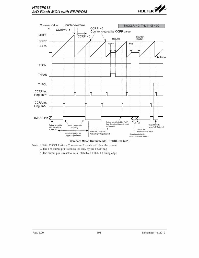
Rev. 2.00 100 November 19, 2019 Rev. 2.00 101 November 19, 2019
HT66F018A/D Flash MCU with EEPROM
HT66F018A/D Flash MCU with EEPROM
Counter Value
0x3FF
CCRPCCRA
TnON
TnPAU
TnPOL
CCRP Int. Flag TnPF
CCRA Int. Flag TnAF
TM O/P Pin
Time
CCRP=0
CCRP > 0
Counter overflowCCRP > 0Counter cleared by CCRP value
Pause
Resume
Stop
Counter Restart
TnCCLR = 0; TnM [1:0] = 00
Output pin set to initial Level Low if TnOC=0
Output Toggle with TnAF flag
Note TnIO [1:0] = 10 Active High Output selectHere TnIO [1:0] = 11
Toggle Output select
Output not affected by TnAF flag. Remains High until reset by TnON bit
Output PinReset to Initial value
Output controlled by other pin-shared function
Output Invertswhen TnPOL is high
Compare Match Output Mode – TnCCLR=0 (n=1)Note: 1. With TnCCLR=0 – a Comparator P match will clear the counter
2. The TM output pin is controlled only by the TnAF flag3. The output pin is reset to initial state by a TnON bit rising edge
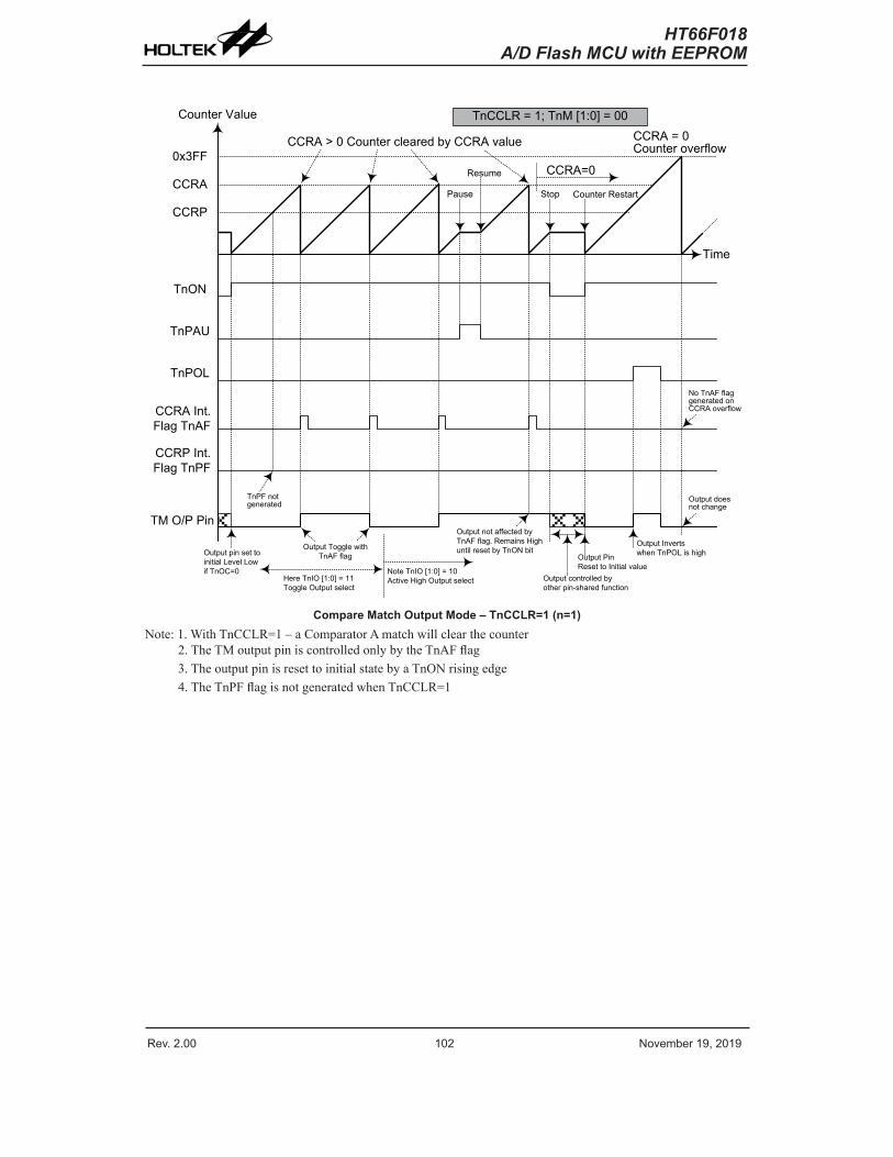
Rev. 2.00 102 November 19, 2019 Rev. 2.00 103 November 19, 2019
HT66F018A/D Flash MCU with EEPROM
HT66F018A/D Flash MCU with EEPROM
Counter Value
0x3FF
CCRP
CCRA
TnON
TnPAU
TnPOL
CCRP Int. Flag TnPF
CCRA Int. Flag TnAF
TM O/P Pin
Time
CCRA=0
CCRA = 0Counter overflowCCRA > 0 Counter cleared by CCRA value
Pause
Resume
Stop Counter Restart
TnCCLR = 1; TnM [1:0] = 00
Output pin set to initial Level Low if TnOC=0
Output Toggle with TnAF flag
Note TnIO [1:0] = 10 Active High Output selectHere TnIO [1:0] = 11
Toggle Output select
Output not affected by TnAF flag. Remains High until reset by TnON bit
Output PinReset to Initial value
Output controlled by other pin-shared function
Output Invertswhen TnPOL is high
TnPF not generated
No TnAF flag generated on CCRA overflow
Output does not change
Compare Match Output Mode – TnCCLR=1 (n=1)Note: 1. With TnCCLR=1 – a Comparator A match will clear the counter
2. The TM output pin is controlled only by the TnAF flag3. The output pin is reset to initial state by a TnON rising edge4. The TnPF flag is not generated when TnCCLR=1

Rev. 2.00 102 November 19, 2019 Rev. 2.00 103 November 19, 2019
HT66F018A/D Flash MCU with EEPROM
HT66F018A/D Flash MCU with EEPROM
Timer/Counter ModeTo select this mode, bits TnM1 and TnM0 in the TMnC1 register should all be set to 11 respectively. The Timer/Counter Mode operates in an identical way to the Compare Match Output Mode generating the same interrupt flags. The exception is that in the Timer/Counter Mode the TM output pin is not used. Therefore the above description and Timing Diagrams for the Compare Match Output Mode can be used to understand its function. As the TM output pin is not used in this mode, the pin can be used as a normal I/O pin or other pin-shared function.
PWM Output ModeTo select this mode, bits TnM1 and TnM0 in the TMnC1 register should be set to 10 respectively and also the TnIO1 and TnIO0 bits should be set to 10 respectively. The PWM function within the TM is useful for applications which require functions such as motor control, heating control, illumination control etc. By providing a signal of fixed frequency but of varying duty cycle on the TM output pin, a square wave AC waveform can be generated with varying equivalent DC RMS values.
As both the period and duty cycle of the PWM waveform can be controlled, the choice of generated waveform is extremely flexible. In the PWM mode, the TnCCLR bit has no effect as the PWM period. Both of the CCRP and CCRA registers are used to generate the PWM waveform, one register is used to clear the internal counter and thus control the PWM waveform frequency, while the other one is used to control the duty cycle. The PWM waveform frequency and duty cycle can therefore be controlled by the values in the CCRA and CCRP registers.
An interrupt flag, one for each of the CCRA and CCRP, will be generated when a compare match occurs from either Comparator A or Comparator P. The TnOC bit in the TMnC1 register is used to select the required polarity of the PWM waveform while the two TnIO1 and TnIO0 bits are used to enable the PWM output or to force the TM output pin to a fixed high or low level. The TnPOL bit is used to reverse the polarity of the PWM output waveform.
10-bit PTM, PWM ModeCCRP 1~1023 0Period 1~1023 1024Duty CCRA
If fSYS=16MHz, TM clock source select fSYS/4, CCRP=512 and CCRA=128,
The PTM PWM output frequency=(fSYS/4) / (2×256)=fSYS/2048=7.8125kHz, duty=128/512=25%,
If the Duty value defined by the CCRA register is equal to or greater than the Period value, then the PWM output duty is 100%.
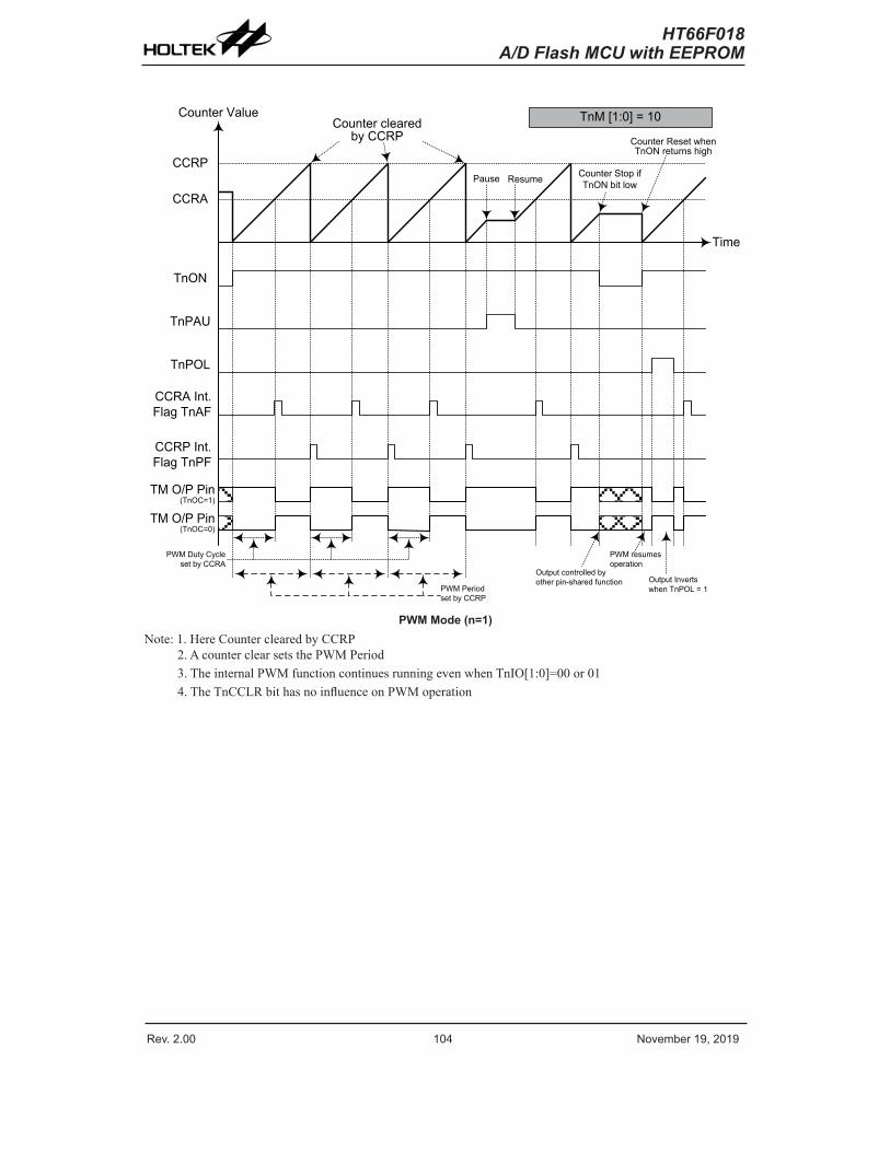
Rev. 2.00 104 November 19, 2019 Rev. 2.00 105 November 19, 2019
HT66F018A/D Flash MCU with EEPROM
HT66F018A/D Flash MCU with EEPROM
Counter Value
CCRP
CCRA
TnON
TnPAU
TnPOL
CCRP Int. Flag TnPF
CCRA Int. Flag TnAF
TM O/P Pin(TnOC=1)
Time
Counter cleared by CCRP
Pause Resume Counter Stop if TnON bit low
Counter Reset when TnON returns high
TnM [1:0] = 10
PWM Duty Cycle set by CCRA
PWM resumes operation
Output controlled by other pin-shared function Output Inverts
when TnPOL = 1PWM Period set by CCRP
TM O/P Pin(TnOC=0)
PWM Mode (n=1)Note: 1. Here Counter cleared by CCRP
2. A counter clear sets the PWM Period3. The internal PWM function continues running even when TnIO[1:0]=00 or 014. The TnCCLR bit has no influence on PWM operation
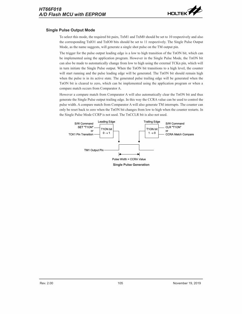
Rev. 2.00 104 November 19, 2019 Rev. 2.00 105 November 19, 2019
HT66F018A/D Flash MCU with EEPROM
HT66F018A/D Flash MCU with EEPROM
Single Pulse Output ModeTo select this mode, the required bit pairs, TnM1 and TnM0 should be set to 10 respectively and also the corresponding TnIO1 and TnIO0 bits should be set to 11 respectively. The Single Pulse Output Mode, as the name suggests, will generate a single shot pulse on the TM output pin.
The trigger for the pulse output leading edge is a low to high transition of the TnON bit, which can be implemented using the application program. However in the Single Pulse Mode, the TnON bit can also be made to automatically change from low to high using the external TCKn pin, which will in turn initiate the Single Pulse output. When the TnON bit transitions to a high level, the counter will start running and the pulse leading edge will be generated. The TnON bit should remain high when the pulse is in its active state. The generated pulse trailing edge will be generated when the TnON bit is cleared to zero, which can be implemented using the application program or when a compare match occurs from Comparator A.
However a compare match from Comparator A will also automatically clear the TnON bit and thus generate the Single Pulse output trailing edge. In this way the CCRA value can be used to control the pulse width. A compare match from Comparator A will also generate TM interrupts. The counter can only be reset back to zero when the TnON bit changes from low to high when the counter restarts. In the Single Pulse Mode CCRP is not used. The TnCCLR bit is also not used.
Single Pulse Generation
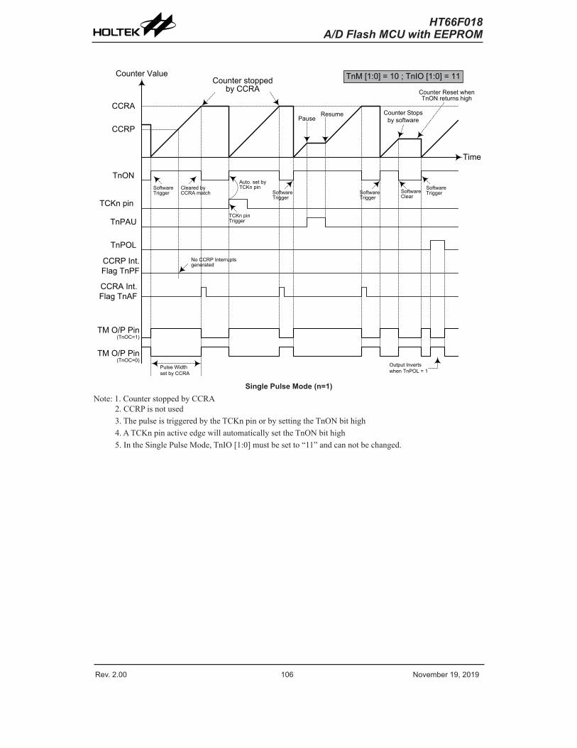
Rev. 2.00 106 November 19, 2019 Rev. 2.00 107 November 19, 2019
HT66F018A/D Flash MCU with EEPROM
HT66F018A/D Flash MCU with EEPROM
Counter Value
CCRP
CCRA
TnON
TnPAU
TnPOL
CCRP Int. Flag TnPF
CCRA Int. Flag TnAF
TM O/P Pin(TnOC=1)
Time
Counter stopped by CCRA
PauseResume Counter Stops
by software
Counter Reset when TnON returns high
TnM [1:0] = 10 ; TnIO [1:0] = 11
Pulse Width set by CCRA
Output Invertswhen TnPOL = 1
No CCRP Interrupts generated
TM O/P Pin(TnOC=0)
TCKn pin
Software Trigger
Cleared by CCRA match
TCKn pin Trigger
Auto. set by TCKn pin
Software Trigger
Software Clear
Software TriggerSoftware
Trigger
Single Pulse Mode (n=1)Note: 1. Counter stopped by CCRA
2. CCRP is not used3. The pulse is triggered by the TCKn pin or by setting the TnON bit high4. A TCKn pin active edge will automatically set the TnON bit high5. In the Single Pulse Mode, TnIO [1:0] must be set to “11” and can not be changed.
Rev. 2.00 106 November 19, 2019 Rev. 2.00 107 November 19, 2019
HT66F018A/D Flash MCU with EEPROM
HT66F018A/D Flash MCU with EEPROM
Capture Input ModeTo select this mode bits TnM1 and TnM0 in the TMnC1 register should be set to 01 respectively. This mode enables external signals to capture and store the present value of the internal counter and can therefore be used for applications such as pulse width measurements. The external signal is supplied on the TPn or TCKn pin, selected by the TnCAPTS bit in the TMnC0 register. The input pin active edge can be either a rising edge, a falling edge or both rising and falling edges; the active edge transition type is selected using the TnIO1 and TnIO0 bits in the TMnC1 register. The counter is started when the TnON bit changes from low to high which is initiated using the application program.
When the required edge transition appears on the TPn or TCKn pin the present value in the counter will be latched into the CCRA register and a TM interrupt generated. Irrespective of what events occur on the TPn or TCKn pin the counter will continue to free run until the TnON bit changes from high to low. When a CCRP compare match occurs the counter will reset back to zero; in this way the CCRP value can be used to control the maximum counter value. When a CCRP compare match occurs from Comparator P, a TM interrupt will also be generated. Counting the number of overflow interrupt signals from the CCRP can be a useful method in measuring long pulse widths. The TnIO1 and TnIO0 bits can select the active trigger edge on the TPn or TCKn pin to be a rising edge, falling edge or both edge types. If the TnIO1 and TnIO0 bits are both set high, then no capture operation will take place irrespective of what happens on the TPn or TCKn pin, however it must be noted that the counter will continue to run.
As the TPn or TCKn pin is pin shared with other functions, care must be taken if the TMn is in the Capture Input Mode. This is because if the pin is setup as an output, then any transitions on this pin may cause an input capture operation to be executed. The TnCCLR, TnOC and TnPOL bits are not used in this Mode.
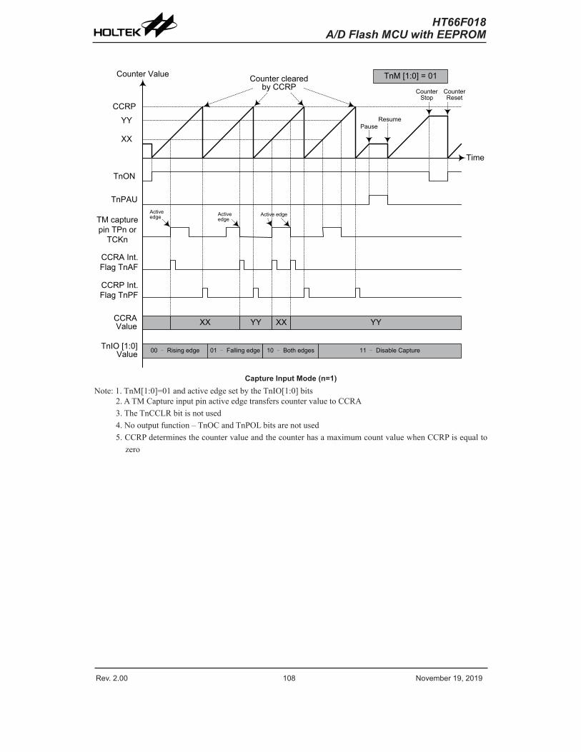
Rev. 2.00 108 November 19, 2019 Rev. 2.00 109 November 19, 2019
HT66F018A/D Flash MCU with EEPROM
HT66F018A/D Flash MCU with EEPROM
Counter Value
YYCCRP
TnON
TnPAU
CCRP Int. Flag TnPF
CCRA Int. Flag TnAF
CCRA Value
Time
Counter cleared by CCRP
PauseResume
Counter Reset
TnM [1:0] = 01
TM capture pin TPn or
TCKn
XX
Counter Stop
TnIO [1:0] Value
XX YY XX YY
Active edge Active
edgeActive edge
00 – Rising edge 01 – Falling edge 10 – Both edges 11 – Disable Capture
Capture Input Mode (n=1)Note: 1. TnM[1:0]=01 and active edge set by the TnIO[1:0] bits
2. A TM Capture input pin active edge transfers counter value to CCRA3. The TnCCLR bit is not used4. No output function – TnOC and TnPOL bits are not used5. CCRP determines the counter value and the counter has a maximum count value when CCRP is equal to
zero
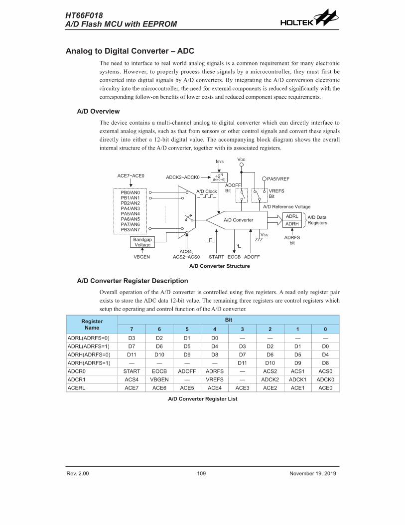
Rev. 2.00 108 November 19, 2019 Rev. 2.00 109 November 19, 2019
HT66F018A/D Flash MCU with EEPROM
HT66F018A/D Flash MCU with EEPROM
Analog to Digital Converter – ADCThe need to interface to real world analog signals is a common requirement for many electronic systems. However, to properly process these signals by a microcontroller, they must first be converted into digital signals by A/D converters. By integrating the A/D conversion electronic circuitry into the microcontroller, the need for external components is reduced significantly with the corresponding follow-on benefits of lower costs and reduced component space requirements.
A/D OverviewThe device contains a multi-channel analog to digital converter which can directly interface to external analog signals, such as that from sensors or other control signals and convert these signals directly into either a 12-bit digital value. The accompanying block diagram shows the overall internal structure of the A/D converter, together with its associated registers.
� � � � � � � � � � � � �
� � � � � � �� � � � � � �� � � � � � �� � � � � � � � � � � � �� � � � � � �� � � � � �� � � � �
� � � � � � � � � � � � � � � � � � � �
� � �� � �
� � � � � � � � � � � � � � � �
� � � � � � � � � � � � � �
� � �
� � � � � � � � � � � � � � � � �
� � � �
� � � � � � � �
� � � � �� � � � � � � � �
� � � � � � �� � � � � � �
� � � � � � � � �
� � �
� � � � � � � �
� � �
� � �� � �
� � � � �� � � � � � �
A/D Converter Structure
A/D Converter Register DescriptionOverall operation of the A/D converter is controlled using five registers. A read only register pair exists to store the ADC data 12-bit value. The remaining three registers are control registers which setup the operating and control function of the A/D converter.
Register Name
Bit7 6 5 4 3 2 1 0
ADRL(ADRFS=0) D3 D2 D1 D0 — — — —ADRL(ADRFS=1) D7 D6 D5 D4 D3 D2 D1 D0ADRH(ADRFS=0) D11 D10 D9 D8 D7 D6 D5 D4ADRH(ADRFS=1) — — — — D11 D10 D9 D8ADCR0 START EOCB ADOFF ADRFS — ACS2 ACS1 ACS0ADCR1 ACS4 VBGEN — VREFS — ADCK2 ADCK1 ADCK0ACERL ACE7 ACE6 ACE5 ACE4 ACE3 ACE2 ACE1 ACE0
A/D Converter Register List
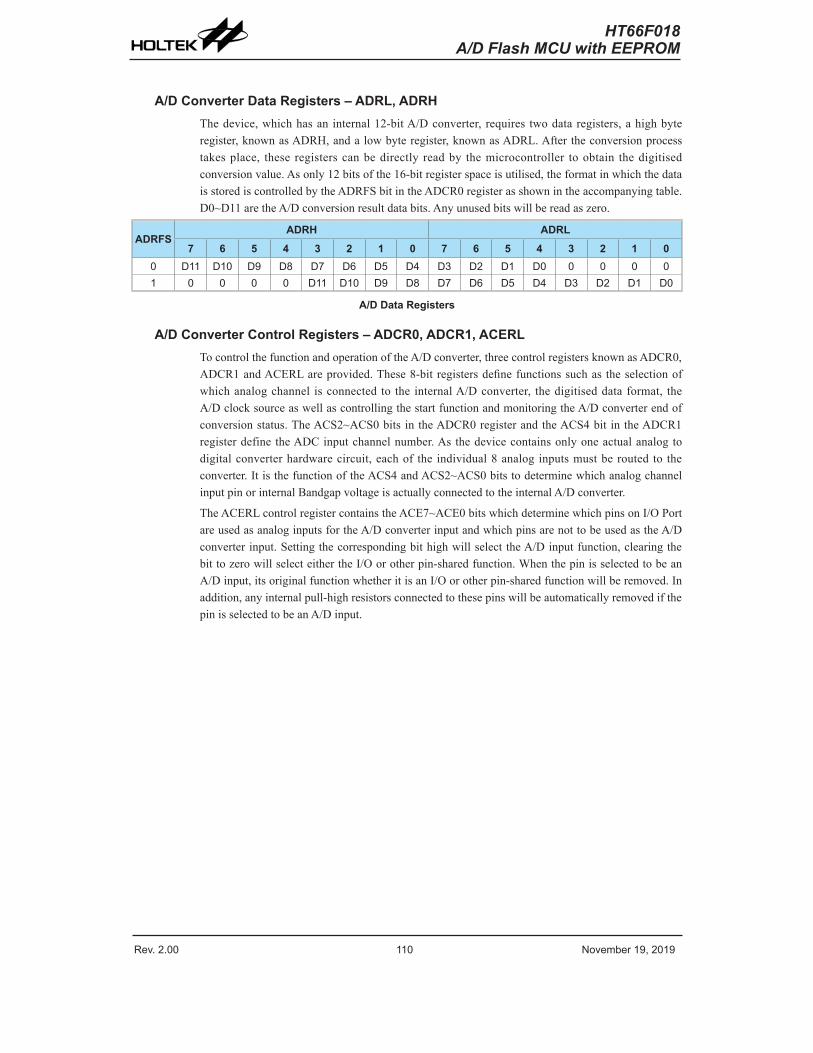
Rev. 2.00 110 November 19, 2019 Rev. 2.00 111 November 19, 2019
HT66F018A/D Flash MCU with EEPROM
HT66F018A/D Flash MCU with EEPROM
A/D Converter Data Registers – ADRL, ADRHThe device, which has an internal 12-bit A/D converter, requires two data registers, a high byte register, known as ADRH, and a low byte register, known as ADRL. After the conversion process takes place, these registers can be directly read by the microcontroller to obtain the digitised conversion value. As only 12 bits of the 16-bit register space is utilised, the format in which the data is stored is controlled by the ADRFS bit in the ADCR0 register as shown in the accompanying table. D0~D11 are the A/D conversion result data bits. Any unused bits will be read as zero.
ADRFSADRH ADRL
7 6 5 4 3 2 1 0 7 6 5 4 3 2 1 00 D11 D10 D9 D8 D7 D6 D5 D4 D3 D2 D1 D0 0 0 0 01 0 0 0 0 D11 D10 D9 D8 D7 D6 D5 D4 D3 D2 D1 D0
A/D Data Registers
A/D Converter Control Registers – ADCR0, ADCR1, ACERLTo control the function and operation of the A/D converter, three control registers known as ADCR0, ADCR1 and ACERL are provided. These 8-bit registers define functions such as the selection of which analog channel is connected to the internal A/D converter, the digitised data format, the A/D clock source as well as controlling the start function and monitoring the A/D converter end of conversion status. The ACS2~ACS0 bits in the ADCR0 register and the ACS4 bit in the ADCR1 register define the ADC input channel number. As the device contains only one actual analog to digital converter hardware circuit, each of the individual 8 analog inputs must be routed to the converter. It is the function of the ACS4 and ACS2~ACS0 bits to determine which analog channel input pin or internal Bandgap voltage is actually connected to the internal A/D converter.
The ACERL control register contains the ACE7~ACE0 bits which determine which pins on I/O Port are used as analog inputs for the A/D converter input and which pins are not to be used as the A/D converter input. Setting the corresponding bit high will select the A/D input function, clearing the bit to zero will select either the I/O or other pin-shared function. When the pin is selected to be an A/D input, its original function whether it is an I/O or other pin-shared function will be removed. In addition, any internal pull-high resistors connected to these pins will be automatically removed if the pin is selected to be an A/D input.
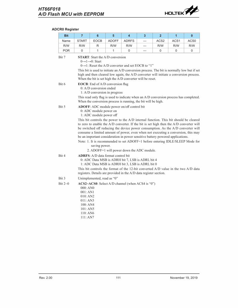
Rev. 2.00 110 November 19, 2019 Rev. 2.00 111 November 19, 2019
HT66F018A/D Flash MCU with EEPROM
HT66F018A/D Flash MCU with EEPROM
ADCR0 RegisterBit 7 6 5 4 3 2 1 0
Name START EOCB ADOFF ADRFS — ACS2 ACS1 ACS0R/W R/W R R/W R/W — R/W R/W R/WPOR 0 1 1 0 — 0 0 0
Bit 7 START: Start the A/D conversion0→1→0: Start0→1: Reset the A/D converter and set EOCB to “1”
This bit is used to initiate an A/D conversion process. The bit is normally low but if set high and then cleared low again, the A/D converter will initiate a conversion process. When the bit is set high the A/D converter will be reset.
Bit 6 EOCB: End of A/D conversion flag0: A/D conversion ended1: A/D conversion in progress
This read only flag is used to indicate when an A/D conversion process has completed. When the conversion process is running, the bit will be high.
Bit 5 ADOFF: ADC module power on/off control bit0: ADC module power on1: ADC module power off
This bit controls the power to the A/D internal function. This bit should be cleared to zero to enable the A/D converter. If the bit is set high then the A/D converter will be switched off reducing the device power consumption. As the A/D converter will consume a limited amount of power, even when not executing a conversion, this may be an important consideration in power sensitive battery powered applications.Note: 1. It is recommended to set ADOFF=1 before entering IDLE/SLEEP Mode for
saving power.2. ADOFF=1 will power down the ADC module.
Bit 4 ADRFS: A/D data format control bit0: ADC Data MSB is ADRH bit 7, LSB is ADRL bit 41: ADC Data MSB is ADRH bit 3, LSB is ADRL bit 0
This bit controls the format of the 12-bit converted A/D value in the two A/D data registers. Details are provided in the A/D data register section.
Bit 3 Unimplemented, read as “0”Bit 2~0 ACS2~ACS0: Select A/D channel (when ACS4 is “0”)
000: AN0001: AN1010: AN2011: AN3100: AN4101: AN5110: AN6111: AN7

Rev. 2.00 112 November 19, 2019 Rev. 2.00 113 November 19, 2019
HT66F018A/D Flash MCU with EEPROM
HT66F018A/D Flash MCU with EEPROM
ADCR1 RegisterBit 7 6 5 4 3 2 1 0
Name ACS4 VBGEN — VREFS — ADCK2 ADCK1 ADCK0R/W R/W R/W — R/W — R/W R/W R/WPOR 0 0 — 0 — 0 0 0
Bit 7 ACS4: select internal Bandgap voltage as ADC input control0: Disable1: Enable
This bit enables Bandgap voltage to be connected to the A/D converter. The VBGEN bit must first have been set to enable the bandgap circuit voltage to be used by the A/D converter. When the ACS4 bit is set high, the bandgap voltage will be routed to the A/D converter and the other A/D input channels disconnected.
Bit 6 VBGEN: internal Bandgap voltage enable control0: Disable1: Enable
This bit controls the internal Bandgap circuit on/off function to the A/D converter. When the bit is set high the bandgap voltage can be used by the A/D converter.
Bit 5 Unimplemented, read as “0”Bit 4 VREFS: Selecte ADC reference voltage
0: Internal ADC power1: VREF pin
This bit is used to select the reference voltage for the A/D converter. If the bit is high, then the A/D converter reference voltage is supplied on the external VREF pin. If the pin is low, then the internal reference is used which is taken from the power supply pin VDD. When the A/D converter reference voltage is supplied on the external VREF pin which is pin-shared with other functions, all of the pin-shared functions except VREF on this pin are disabled.
Bit 3 Unimplemented, read as “0”Bit 2~0 ADCK2~ADCK0: Select ADC clock source
000: fSYS
001: fSYS/2010: fSYS/4011: fSYS/8100: fSYS/16101: fSYS/32110: fSYS/64111: Undefined
These three bits are used to select the clock source for the A/D converter.

Rev. 2.00 112 November 19, 2019 Rev. 2.00 113 November 19, 2019
HT66F018A/D Flash MCU with EEPROM
HT66F018A/D Flash MCU with EEPROM
ACERL RegisterBit 7 6 5 4 3 2 1 0
Name ACE7 ACE6 ACE5 ACE4 ACE3 ACE2 ACE1 ACE0R/W R/W R/W R/W R/W R/W R/W R/W R/WPOR 1 1 1 1 1 1 1 1
Bit 7 ACE7: Define PB3 is A/D input or not0: Not A/D input1: A/D input, AN7
Bit 6 ACE6: Define PA7 is A/D input or not0: Not A/D input1: A/D input, AN6
Bit 5 ACE5: Define PA6 is A/D input or not0: Not A/D input1: A/D input, AN5
Bit 4 ACE4: Define PA5 is A/D input or not0: Not A/D input1: A/D input, AN4
Bit 3 ACE3: Define PA4 is A/D input or not0: Not A/D input1: A/D input, AN3
Bit 2 ACE2: Define PB2 is A/D input or not0: Not A/D input1: A/D input, AN2
Bit 1 ACE1: Define PB1 is A/D input or not0: Not A/D input1: A/D input, AN1
Bit 0 ACE0: Define PB0 is A/D input or not0: Not A/D input1: A/D input, AN0

Rev. 2.00 114 November 19, 2019 Rev. 2.00 115 November 19, 2019
HT66F018A/D Flash MCU with EEPROM
HT66F018A/D Flash MCU with EEPROM
A/D Operation The START bit in the ADCR0 register is used to start and reset the A/D converter. When the microcontroller sets this bit from low to high and then low again, an analog to digital conversion cycle will be initiated. When the START bit is brought from low to high but not low again, the EOCB bit in the ADCR0 register will be set high and the analog to digital converter will be reset. It is the START bit that is used to control the overall start operation of the internal analog to digital converter.
The EOCB bit in the ADCR0 register is used to indicate when the analog to digital conversion process is complete. This bit will be automatically set to “0” by the microcontroller after a conversion cycle has ended. In addition, the corresponding A/D interrupt request flag will be set in the interrupt control register, and if the interrupts are enabled, an appropriate internal interrupt signal will be generated. This A/D internal interrupt signal will direct the program flow to the associated A/D internal interrupt address for processing. If the A/D internal interrupt is disabled, the microcontroller can be used to poll the EOCB bit in the ADCR0 register to check whether it has been cleared as an alternative method of detecting the end of an A/D conversion cycle.
The clock source for the A/D converter, which originates from the system clock fSYS, can be chosen to be either fSYS or a subdivided version of fSYS The division ratio value is determined by the ADCK2~ADCK0 bits in the ADCR1 register.
Although the A/D clock source is determined by the system clock fSYS, and by bits ADCK2~ADCK0, there are some limitations on the A/D clock source speed range that can be selected. As the recommended range of permissible A/D clock period, tADCK, is from 0.5μs to 10μs, care must be taken for selected system clock frequencies. For example, if the system clock operates at a frequency of 4MHz, the ADCK2~ADCK0 bits should not be set to 000B or 110B. Doing so will give A/D clock periods that are less than the minimum A/D clock period or greater than the maximum A/D clock period which may result in inaccurate A/D conversion values.
Refer to the following table for examples, where values marked with an asterisk * show where, depending upon the device, special care must be taken, as the values may be less than the specified minimum A/D Clock Period.
fSYS
A/D Clock Period (tADCK)ADCK2,ADCK1,ADCK0
=000(fSYS)
ADCK2,ADCK1,ADCK0
=001(fSYS/2)
ADCK2,ADCK1, ADCK0
=010(fSYS/4)
ADCK2,ADCK1, ADCK0
=011(fSYS/8)
ADCK2,ADCK1,ADCK0
=100(fSYS/16)
ADCK2,ADCK1,ADCK0
=101(fSYS/32)
ADCK2,ADCK1,ADCK0
=110(fSYS/64)
ADCK2,ADCK1,ADCK0
=111
1MHz 1μs 2μs 4μs 8μs 16μs* 32μs* 64μs* Undefined2MHz 500ns 1μs 2μs 4μs 8μs 16μs* 32μs* Undefined4MHz 250ns* 500ns 1μs 2μs 4μs 8μs 16μs* Undefined8MHz 125ns* 250ns* 500ns 1μs 2μs 4μs 8μs Undefined
12MHz 83ns* 167ns* 333ns* 667ns 1.33μs 2.67μs 5.33μs Undefined
A/D Clock Period Examples
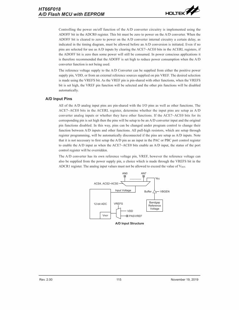
Rev. 2.00 114 November 19, 2019 Rev. 2.00 115 November 19, 2019
HT66F018A/D Flash MCU with EEPROM
HT66F018A/D Flash MCU with EEPROM
Controlling the power on/off function of the A/D converter circuitry is implemented using the ADOFF bit in the ADCR0 register. This bit must be zero to power on the A/D converter. When the ADOFF bit is cleared to zero to power on the A/D converter internal circuitry a certain delay, as indicated in the timing diagram, must be allowed before an A/D conversion is initiated. Even if no pins are selected for use as A/D inputs by clearing the ACE7~ACE0 bits in the ACERL registers, if the ADOFF bit is zero then some power will still be consumed. In power conscious applications it is therefore recommended that the ADOFF is set high to reduce power consumption when the A/D converter function is not being used.
The reference voltage supply to the A/D Converter can be supplied from either the positive power supply pin, VDD, or from an external reference sources supplied on pin VREF. The desired selection is made using the VREFS bit. As the VREF pin is pin-shared with other functions, when the VREFS bit is set high, the VREF pin function will be selected and the other pin functions will be disabled automatically.
A/D Input PinsAll of the A/D analog input pins are pin-shared with the I/O pins as well as other functions. The ACE7~ACE0 bits in the ACERL register, determine whether the input pins are setup as A/D converter analog inputs or whether they have other functions. If the ACE7~ACE0 bits for its corresponding pin is set high then the pins will be setup to be an A/D converter input and the original pin functions disabled. In this way, pins can be changed under program control to change their function between A/D inputs and other functions. All pull-high resistors, which are setup through register programming, will be automatically disconnected if the pins are setup as A/D inputs. Note that it is not necessary to first setup the A/D pin as an input in the PAC or PBC port control register to enable the A/D input as when the ACE7~ACE0 bits enable an A/D input, the status of the port control register will be overridden.
The A/D converter has its own reference voltage pin, VREF, however the reference voltage can also be supplied from the power supply pin, a choice which is made through the VREFS bit in the ADCR1 register. The analog input values must not be allowed to exceed the value of VREF.
� � � � � �
� � � � �� � � � � �
� � � � � � � �
� � �
� � � �
� � � �
� � � � � � � � � � � � � � �� � � � � � � � �� � � � � � �
� � � � � � � � � � � � �
� � � � � � � � � �
� � �
A/D Input Structure
Rev. 2.00 116 November 19, 2019 Rev. 2.00 117 November 19, 2019
HT66F018A/D Flash MCU with EEPROM
HT66F018A/D Flash MCU with EEPROM
Summary of A/D Conversion Steps The following summarises the individual steps that should be executed in order to implement an A/D conversion process.
• Step 1 Select the required A/D conversion clock by correctly programming bits ADCK2~ADCK0 in the ADCR1 register.
• Step 2 Enable the A/D by clearing the ADOFF bit in the ADCR0 register to zero.
• Step 3Select which channel is to be connected to the internal A/D converter by correctly programming the ACS4 and ACS2~ACS0 bits which are also contained in the ADCR1 and ADCR0 register.
• Step 4Select which pins are to be used as A/D inputs and configure them by correctly programming the ACE7~ACE0 bits in the ACERL register.
• Step 5 If the interrupts are to be used, the interrupt control registers must be correctly configured to ensure the A/D converter interrupt function is active. The master interrupt control bit, EMI, and the A/D converter interrupt bit, ADE, must both be set high to do this.
• Step 6 The analog to digital conversion process can now be initialised by setting the START bit in the ADCR0 register from low to high and then low again. Note that this bit should have been originally cleared to zero.
• Step 7To check when the analog to digital conversion process is complete, the EOCB bit in the ADCR0 register can be polled. The conversion process is complete when this bit goes low. When this occurs the A/D data registers ADRL and ADRH can be read to obtain the conversion value. As an alternative method, if the interrupts are enabled and the stack is not full, the program can wait for an A/D interrupt to occur.
Note: When checking for the end of the conversion process, if the method of polling the EOCB bit in the ADCR0 register is used, the interrupt enable step above can be omitted.
The accompanying diagram shows graphically the various stages involved in an analog to digital conversion process and its associated timing. After an A/D conversion process has been initiated by the application program, the microcontroller internal hardware will begin to carry out the conversion, during which time the program can continue with other functions. The time taken for the A/D conversion is 16tADCK where tADCK is equal to the A/D clock period.

Rev. 2.00 116 November 19, 2019 Rev. 2.00 117 November 19, 2019
HT66F018A/D Flash MCU with EEPROM
HT66F018A/D Flash MCU with EEPROM
� � � �� � � � � � � � � � � � � � � � � � �
� � � � � � � � � �
� � � �
� �
� � � � �� � � � � � �
� � � � � � � �� � � � �
� � � � � � � � �� � � � � � � � � �� � � � � � � � � � � � � � � � � � � � � � � � � � � �
� � � � � � � � � � � � � � � � � � �
� � � � � � � � � � �� � � � � � � � � �
� � � � � � � � �� � � � � � � � �
� � � � � � � � � � � � � � � �� � � � � �
� � � � �
� � � � � � � � � � �� � � � � � � � � �
� � � � � � � � �� � � � � � � � �
� � � � �
� � � � � � � � � � �� � � � � � � � � �
� � � � � � � � �� � � � � � � � �
� � � � � � � � �� � � � � � � � � �
� � � � � � � � � � � � � � � �� � � � � �
� � � � �� �
� � � �
� � � �� � � � � � � � � � � � � � � � � � �
� � �
� � � �
� � � � � � � � � �
A/D Conversion Timing
Programming ConsiderationsDuring microcontroller operations where the A/D converter is not being used, the A/D internal circuitry can be switched off to reduce power consumption, by setting bit ADOFF high in the ADCR0 register. When this happens, the internal A/D converter circuits will not consume power irrespective of what analog voltage is applied to their input lines. If the A/D converter input lines are used as normal I/Os, then care must be taken as if the input voltage is not at a valid logic level, then this may lead to some increase in power consumption.
The power-on reset condition of the A/D converter control registers will ensure that the shared function pins are setup as A/D converter inputs. If any of the A/D converter input pins are to be used for functions, then the A/D converter control register bits must be properly setup to disable the A/D input configuration.
A/D Transfer FunctionAs the device contains a 12-bit A/D converter, its full-scale converted digitised value is equal to FFFH. Since the full-scale analog input value is equal to the VDD or VREF voltage, this gives a single bit analog input value of VDD or VREF divided by 4096.
1 LSB=(VDD or VREF) ÷ 4096
The A/D Converter input voltage value can be calculated using the following equation:
A/D input voltage=A/D output digital value×(VDD or VREF) ÷ 4096
The diagram shows the ideal transfer function between the analog input value and the digitised output value for the A/D converter. Except for the digitised zero value, the subsequent digitised values will change at a point 0.5 LSB below where they would change without the offset, and the last full scale digitised value will change at a point 1.5 LSB below the VDD or VREF level.
Rev. 2.00 118 November 19, 2019 Rev. 2.00 119 November 19, 2019
HT66F018A/D Flash MCU with EEPROM
HT66F018A/D Flash MCU with EEPROM
Ideal A/D Transfer Function
A/D Programming ExampleThe following two programming examples illustrate how to setup and implement an A/D conversion. In the first example, the method of polling the EOCB bit in the ADCR0 register is used to detect when the conversion cycle is complete, whereas in the second example, the A/D interrupt is used to determine when the conversion is complete.
Example: using an EOCB polling method to detect the end of conversionclr ADE ; disable ADC interruptmov a, 03Hmov ADCR1, a ; select fSYS/8 as A/D clock and switch off the bandgap circuityclr ADOFFmov a, 0Fh ; setup ACERL to configure pins AN0~AN3mov ACERL, amov a, 00hmov ADCR0, a ; enable and connect AN0 channel to A/D converter: : Start_conversion: clr START set START ; reset A/D clr START ; start A/D Polling_EOC: sz EOCB ; poll the ADCR0 register EOCB bit to detect end of A/D conversion jmp polling_EOC ; continue polling mov a, ADRL ; read low byte conversion result value mov adrl_buffer, a ; save result to user defined register mov a, ADRH ; read high byte conversion result value mov adrh_buffer, a ; save result to user defined register : jmp start_conversion ; start next A/D conversion
Note: To power off the ADC, it is necessary to set ADOFF as “1”.
Rev. 2.00 118 November 19, 2019 Rev. 2.00 119 November 19, 2019
HT66F018A/D Flash MCU with EEPROM
HT66F018A/D Flash MCU with EEPROM
Example: using the interrupt method to detect the end of conversionclr ADE ; disable ADC interruptmov a, 03Hmov ADCR1, a ; select fSYS/8 as A/D clock and switch off the bandgap circuityclr ADOFFmov a, 0Fh ; setup ACERL to configure pins AN0~AN3mov ACERL, amov a, 00hmov ADCR0, a ; enable and connect AN0 channel to A/D converter: : Start_conversion: clr START set START ; reset A/D clr START ; start A/D clr ADF ; clear ADC interrupt request flag set ADE ; enable ADC interrupt set EMI ; enable global interrupt : : ; ADC interrupt service routine ADC_: mov acc_stack, a ; save ACC to user defined memory mov a, STATUS mov status_stack, a ; save STATUS to user defined memory : : mov a, ADRL ; read low byte conversion result value mov adrl_buffer, a ; save result to user defined register mov a, ADRH ; read high byte conversion result value mov adrh_buffer, a ; save result to user defined register : : EXIT_ISR: mov a, status_stack mov STATUS, a ; restore STATUS from user defined memory mov a, acc_stack ; restore ACC from user defined memory clr ADF ; clear ADC interrupt flag reti
Note: To power off the ADC, it is necessary to set ADOFF as “1”.
Rev. 2.00 120 November 19, 2019 Rev. 2.00 121 November 19, 2019
HT66F018A/D Flash MCU with EEPROM
HT66F018A/D Flash MCU with EEPROM
ComparatorsAn analog comparator is contained within the device. The comparator function offers flexibility via their register controlled features such as power-down, polarity select, hysteresis etc. In sharing their pins with normal I/O pins the comparators do not waste precious I/O pins if there functions are otherwise unused.
� �
� �
� � � � � � � �
� �
� � �
Comparator
Comparator OperationThe device contains a comparator function which is used to compare two analog voltages and provide an output based on their difference. Full control over the internal comparators is provided via the control register CPC assigned to the comparator. The comparator output is recorded via a bit in the control register, but can also be transferred out onto a shared I/O pin. Additional comparator functions include, output polarity, hysteresis functions and power down control.
Any pull-high resistors connected to the shared comparator input pins will be automatically disconnected when the comparator is enabled. As the comparator inputs approach their switching level, some spurious output signals may be generated on the comparator output due to the slow rising or falling nature of the input signals. This can be minimised by selecting the hysteresis function will apply a small amount of positive feedback to the comparator. Ideally the comparator should switch at the point where the positive and negative inputs signals are at the same voltage level, however, unavoidable input offsets introduce some uncertainties here. The hysteresis function, if enabled, also increases the switching offset value.
Comparator InterruptThe comparator possesses its own interrupt function. When the comparator output changes state, its relevant interrupt flag will be set, and if the corresponding interrupt enable bit is set, then a jump to its relevant interrupt vector will be executed. Note that it is the changing state of the COUT bit and not the output pin which generates an interrupt. If the microcontroller is in the SLEEP or IDLE Mode and the Comparator is enabled, then if the external input lines cause the Comparator output to change state, the resulting generated interrupt flag will also generate a wake-up. If it is required to disable a wake-up from occurring, then the interrupt flag should be first set high before entering the SLEEP or IDLE Mode.
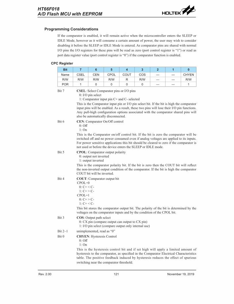
Rev. 2.00 120 November 19, 2019 Rev. 2.00 121 November 19, 2019
HT66F018A/D Flash MCU with EEPROM
HT66F018A/D Flash MCU with EEPROM
Programming ConsiderationsIf the comparator is enabled, it will remain active when the microcontroller enters the SLEEP or IDLE Mode, however as it will consume a certain amount of power, the user may wish to consider disabling it before the SLEEP or IDLE Mode is entered. As comparator pins are shared with normal I/O pins the I/O registers for these pins will be read as zero (port control register is “1”) or read as port data register value (port control register is “0”) if the comparator function is enabled.
CPC RegisterBit 7 6 5 4 3 2 1 0
Name CSEL CEN CPOL COUT COS — — CHYENR/W R/W R/W R/W R R/W — — R/WPOR 1 0 0 0 0 — — 1
Bit 7 CSEL: Select Comparator pins or I/O pins0: I/O pin select1: Comparator input pin C+ and C- selected
This is the Comparator input pin or I/O pin select bit. If the bit is high the comparator input pins will be enabled. As a result, these two pins will lose their I/O pin functions. Any pull-high configuration options associated with the comparator shared pins will also be automatically disconnected.
Bit 6 CEN: Comparator On/Off control0: Off1: On
This is the Comparator on/off control bit. If the bit is zero the comparator will be switched off and no power consumed even if analog voltages are applied to its inputs. For power sensitive applications this bit should be cleared to zero if the comparator is not used or before the device enters the SLEEP or IDLE mode.
Bit 5 CPOL: Comparator output polarity0: output not inverted1: output inverted
This is the comparator polarity bit. If the bit is zero then the COUT bit will reflect the non-inverted output condition of the comparator. If the bit is high the comparator COUT bit will be inverted.
Bit 4 COUT: Comparator output bitCPOL=0
0: C+ < C-1: C+ > C-
CPOL=10: C+ > C-1: C+ < C-
This bit stores the comparator output bit. The polarity of the bit is determined by the voltages on the comparator inputs and by the condition of the CPOL bit.
Bit 3 COS: Output path select0: CX pin (compare output can output to CX pin)1: I/O pin select (compare output only internal use)
Bit 2~1 unimplemented, read as “0”Bit 0 CHYEN: Hysteresis Control
0: Off1: On
This is the hysteresis control bit and if set high will apply a limited amount of hysteresis to the comparator, as specified in the Comparator Electrical Characteristics table. The positive feedback induced by hysteresis reduces the effect of spurious switching near the comparator threshold.
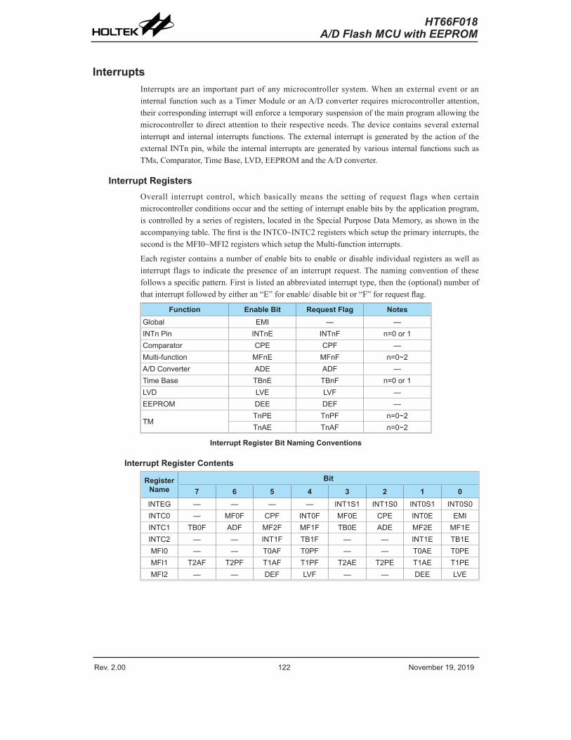
Rev. 2.00 122 November 19, 2019 Rev. 2.00 123 November 19, 2019
HT66F018A/D Flash MCU with EEPROM
HT66F018A/D Flash MCU with EEPROM
InterruptsInterrupts are an important part of any microcontroller system. When an external event or an internal function such as a Timer Module or an A/D converter requires microcontroller attention, their corresponding interrupt will enforce a temporary suspension of the main program allowing the microcontroller to direct attention to their respective needs. The device contains several external interrupt and internal interrupts functions. The external interrupt is generated by the action of the external INTn pin, while the internal interrupts are generated by various internal functions such as TMs, Comparator, Time Base, LVD, EEPROM and the A/D converter.
Interrupt RegistersOverall interrupt control, which basically means the setting of request flags when certain microcontroller conditions occur and the setting of interrupt enable bits by the application program, is controlled by a series of registers, located in the Special Purpose Data Memory, as shown in the accompanying table. The first is the INTC0~INTC2 registers which setup the primary interrupts, the second is the MFI0~MFI2 registers which setup the Multi-function interrupts.
Each register contains a number of enable bits to enable or disable individual registers as well as interrupt flags to indicate the presence of an interrupt request. The naming convention of these follows a specific pattern. First is listed an abbreviated interrupt type, then the (optional) number of that interrupt followed by either an “E” for enable/ disable bit or “F” for request flag.
Function Enable Bit Request Flag NotesGlobal EMI — —INTn Pin INTnE INTnF n=0 or 1Comparator CPE CPF —Multi-function MFnE MFnF n=0~2A/D Converter ADE ADF —Time Base TBnE TBnF n=0 or 1LVD LVE LVF —EEPROM DEE DEF —
TMTnPE TnPF n=0~2TnAE TnAF n=0~2
Interrupt Register Bit Naming Conventions
Interrupt Register Contents
Register Name
Bit7 6 5 4 3 2 1 0
INTEG — — — — INT1S1 INT1S0 INT0S1 INT0S0INTC0 — MF0F CPF INT0F MF0E CPE INT0E EMIINTC1 TB0F ADF MF2F MF1F TB0E ADE MF2E MF1EINTC2 — — INT1F TB1F — — INT1E TB1EMFI0 — — T0AF T0PF — — T0AE T0PEMFI1 T2AF T2PF T1AF T1PF T2AE T2PE T1AE T1PEMFI2 — — DEF LVF — — DEE LVE
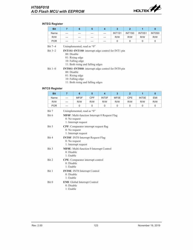
Rev. 2.00 122 November 19, 2019 Rev. 2.00 123 November 19, 2019
HT66F018A/D Flash MCU with EEPROM
HT66F018A/D Flash MCU with EEPROM
INTEG RegisterBit 7 6 5 4 3 2 1 0
Name — — — — INT1S1 INT1S0 INT0S1 INT0S0R/W — — — — R/W R/W R/W R/WPOR — — — — 0 0 0 0
Bit 7~4 Unimplemented, read as “0”Bit 3~2 INT1S1~INT1S0: interrupt edge control for INT1 pin
00: Disable01: Rising edge10: Falling edge11: Both rising and falling edges
Bit 1~0 INT0S1~INT0S0: interrupt edge control for INT0 pin00: Disable01: Rising edge10: Falling edge11: Both rising and falling edges
INTC0 RegisterBit 7 6 5 4 3 2 1 0
Name — MF0F CPF INT0F MF0E CPE INT0E EMIR/W — R/W R/W R/W R/W R/W R/W R/WPOR — 0 0 0 0 0 0 0
Bit 7 Unimplemented, read as “0”Bit 6 MF0F: Multi-function Interrupt 0 Request Flag
0: No request1: Interrupt request
Bit 5 CPF: Comparator interrupt request flag0: No request1: Interrupt request
Bit 4 INT0F: INT0 Interrupt Request Flag0: No request1: Interrupt request
Bit 3 MF0E: Multi-function 0 Interrupt Control0: Disable1: Enable
Bit 2 CPE: Comparator interrupt control0: Disable1: Enable
Bit 1 INT0E: INT0 Interrupt Control0: Disable1: Enable
Bit 0 EMI: Global Interrupt Control0: Disable1: Enable
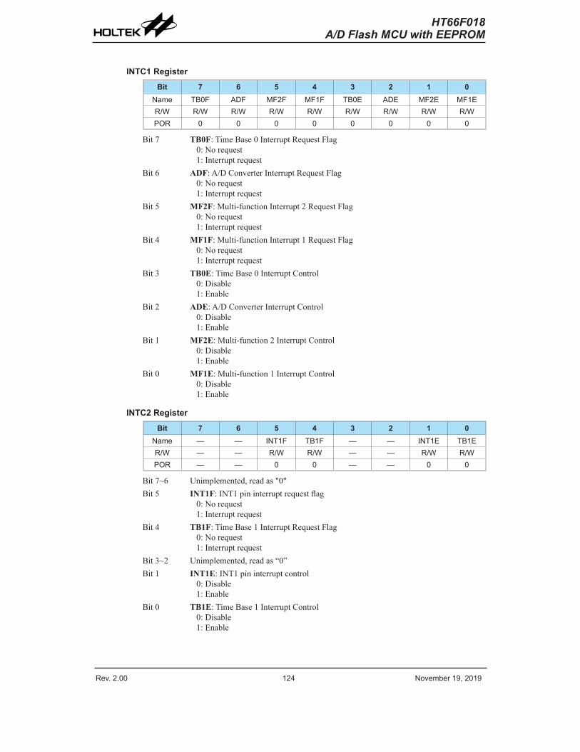
Rev. 2.00 124 November 19, 2019 Rev. 2.00 125 November 19, 2019
HT66F018A/D Flash MCU with EEPROM
HT66F018A/D Flash MCU with EEPROM
INTC1 RegisterBit 7 6 5 4 3 2 1 0
Name TB0F ADF MF2F MF1F TB0E ADE MF2E MF1ER/W R/W R/W R/W R/W R/W R/W R/W R/WPOR 0 0 0 0 0 0 0 0
Bit 7 TB0F: Time Base 0 Interrupt Request Flag0: No request1: Interrupt request
Bit 6 ADF: A/D Converter Interrupt Request Flag0: No request1: Interrupt request
Bit 5 MF2F: Multi-function Interrupt 2 Request Flag0: No request1: Interrupt request
Bit 4 MF1F: Multi-function Interrupt 1 Request Flag0: No request1: Interrupt request
Bit 3 TB0E: Time Base 0 Interrupt Control0: Disable1: Enable
Bit 2 ADE: A/D Converter Interrupt Control0: Disable1: Enable
Bit 1 MF2E: Multi-function 2 Interrupt Control0: Disable1: Enable
Bit 0 MF1E: Multi-function 1 Interrupt Control0: Disable1: Enable
INTC2 RegisterBit 7 6 5 4 3 2 1 0
Name — — INT1F TB1F — — INT1E TB1ER/W — — R/W R/W — — R/W R/WPOR — — 0 0 — — 0 0
Bit 7~6 Unimplemented, read as "0"Bit 5 INT1F: INT1 pin interrupt request flag
0: No request1: Interrupt request
Bit 4 TB1F: Time Base 1 Interrupt Request Flag0: No request1: Interrupt request
Bit 3~2 Unimplemented, read as “0”Bit 1 INT1E: INT1 pin interrupt control
0: Disable1: Enable
Bit 0 TB1E: Time Base 1 Interrupt Control0: Disable1: Enable
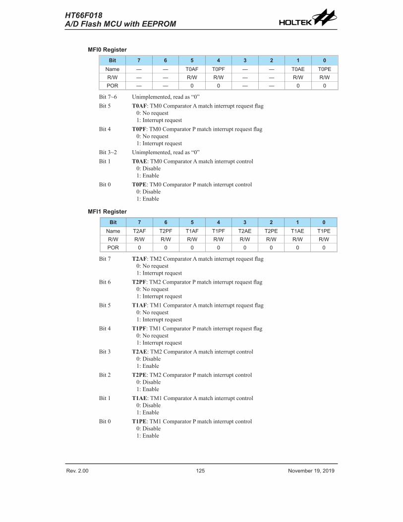
Rev. 2.00 124 November 19, 2019 Rev. 2.00 125 November 19, 2019
HT66F018A/D Flash MCU with EEPROM
HT66F018A/D Flash MCU with EEPROM
MFI0 RegisterBit 7 6 5 4 3 2 1 0
Name — — T0AF T0PF — — T0AE T0PER/W — — R/W R/W — — R/W R/WPOR — — 0 0 — — 0 0
Bit 7~6 Unimplemented, read as “0”Bit 5 T0AF: TM0 Comparator A match interrupt request flag
0: No request1: Interrupt request
Bit 4 T0PF: TM0 Comparator P match interrupt request flag0: No request1: Interrupt request
Bit 3~2 Unimplemented, read as “0”Bit 1 T0AE: TM0 Comparator A match interrupt control
0: Disable1: Enable
Bit 0 T0PE: TM0 Comparator P match interrupt control0: Disable1: Enable
MFI1 RegisterBit 7 6 5 4 3 2 1 0
Name T2AF T2PF T1AF T1PF T2AE T2PE T1AE T1PER/W R/W R/W R/W R/W R/W R/W R/W R/WPOR 0 0 0 0 0 0 0 0
Bit 7 T2AF: TM2 Comparator A match interrupt request flag0: No request1: Interrupt request
Bit 6 T2PF: TM2 Comparator P match interrupt request flag0: No request1: Interrupt request
Bit 5 T1AF: TM1 Comparator A match interrupt request flag0: No request1: Interrupt request
Bit 4 T1PF: TM1 Comparator P match interrupt request flag0: No request1: Interrupt request
Bit 3 T2AE: TM2 Comparator A match interrupt control0: Disable1: Enable
Bit 2 T2PE: TM2 Comparator P match interrupt control0: Disable1: Enable
Bit 1 T1AE: TM1 Comparator A match interrupt control0: Disable1: Enable
Bit 0 T1PE: TM1 Comparator P match interrupt control0: Disable1: Enable
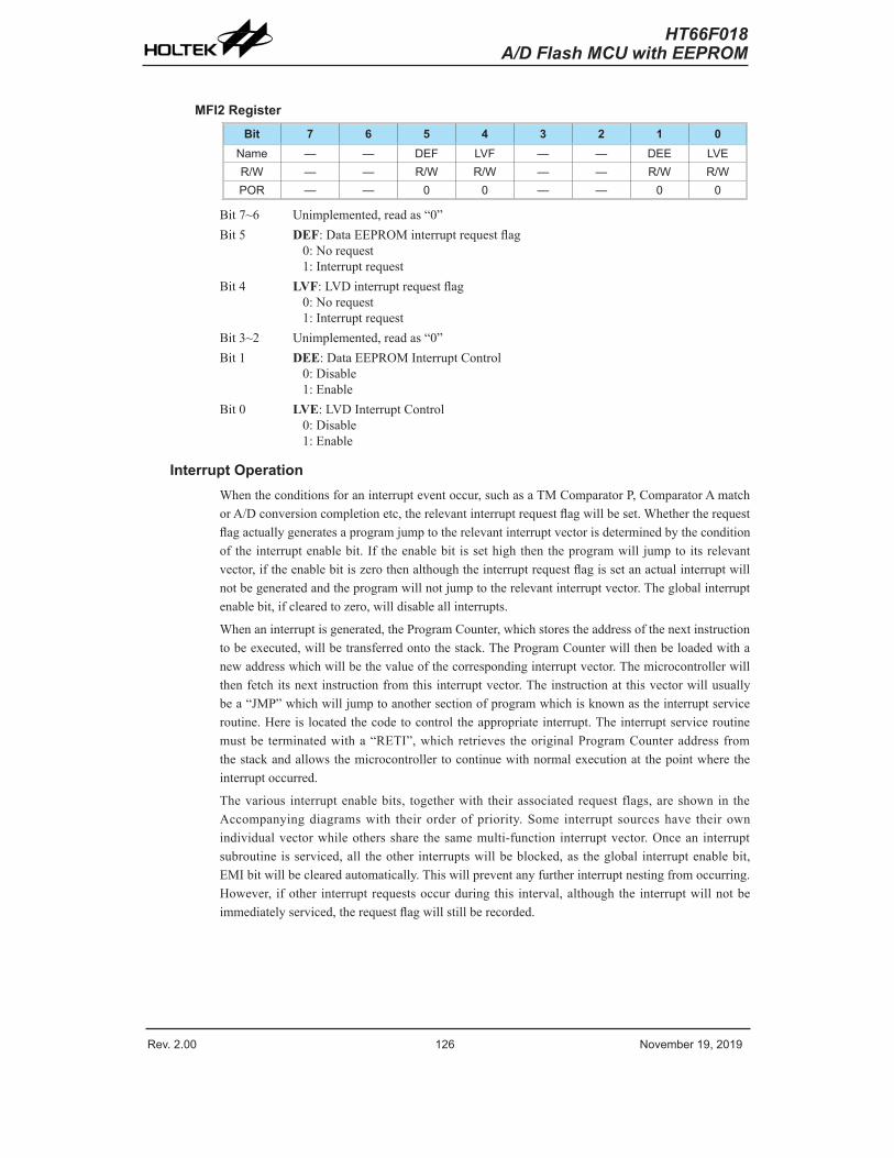
Rev. 2.00 126 November 19, 2019 Rev. 2.00 127 November 19, 2019
HT66F018A/D Flash MCU with EEPROM
HT66F018A/D Flash MCU with EEPROM
MFI2 RegisterBit 7 6 5 4 3 2 1 0
Name — — DEF LVF — — DEE LVER/W — — R/W R/W — — R/W R/WPOR — — 0 0 — — 0 0
Bit 7~6 Unimplemented, read as “0”Bit 5 DEF: Data EEPROM interrupt request flag
0: No request1: Interrupt request
Bit 4 LVF: LVD interrupt request flag0: No request1: Interrupt request
Bit 3~2 Unimplemented, read as “0”Bit 1 DEE: Data EEPROM Interrupt Control
0: Disable1: Enable
Bit 0 LVE: LVD Interrupt Control0: Disable1: Enable
Interrupt OperationWhen the conditions for an interrupt event occur, such as a TM Comparator P, Comparator A match or A/D conversion completion etc, the relevant interrupt request flag will be set. Whether the request flag actually generates a program jump to the relevant interrupt vector is determined by the condition of the interrupt enable bit. If the enable bit is set high then the program will jump to its relevant vector, if the enable bit is zero then although the interrupt request flag is set an actual interrupt will not be generated and the program will not jump to the relevant interrupt vector. The global interrupt enable bit, if cleared to zero, will disable all interrupts.
When an interrupt is generated, the Program Counter, which stores the address of the next instruction to be executed, will be transferred onto the stack. The Program Counter will then be loaded with a new address which will be the value of the corresponding interrupt vector. The microcontroller will then fetch its next instruction from this interrupt vector. The instruction at this vector will usually be a “JMP” which will jump to another section of program which is known as the interrupt service routine. Here is located the code to control the appropriate interrupt. The interrupt service routine must be terminated with a “RETI”, which retrieves the original Program Counter address from the stack and allows the microcontroller to continue with normal execution at the point where the interrupt occurred.
The various interrupt enable bits, together with their associated request flags, are shown in the Accompanying diagrams with their order of priority. Some interrupt sources have their own individual vector while others share the same multi-function interrupt vector. Once an interrupt subroutine is serviced, all the other interrupts will be blocked, as the global interrupt enable bit, EMI bit will be cleared automatically. This will prevent any further interrupt nesting from occurring. However, if other interrupt requests occur during this interval, although the interrupt will not be immediately serviced, the request flag will still be recorded.
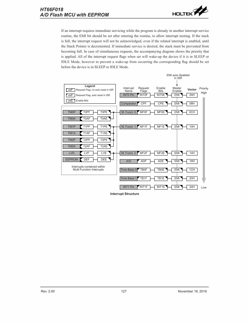
Rev. 2.00 126 November 19, 2019 Rev. 2.00 127 November 19, 2019
HT66F018A/D Flash MCU with EEPROM
HT66F018A/D Flash MCU with EEPROM
If an interrupt requires immediate servicing while the program is already in another interrupt service routine, the EMI bit should be set after entering the routine, to allow interrupt nesting. If the stack is full, the interrupt request will not be acknowledged, even if the related interrupt is enabled, until the Stack Pointer is decremented. If immediate service is desired, the stack must be prevented from becoming full. In case of simultaneous requests, the accompanying diagram shows the priority that is applied. All of the interrupt request flags when set will wake-up the device if it is in SLEEP or IDLE Mode, however to prevent a wake-up from occurring the corresponding flag should be set before the device is in SLEEP or IDLE Mode.
INT0 Pin
INT1 Pin
INT0F
INT1F
INT0E
INT1E
EMI 04H
EMI 08H
EMI 0CH
EMI 10H
Time Base 0 TB0F TB0E
TM2P T2PF T2PE
EMI 1CH
Interrupt Name
Request Flags
Enable Bits
Master Enable Vector
EMI auto disabled in ISR
PriorityHigh
Low
TM0P T0PF T0PE
TM0A T0AF T0AE
M. Funct. 0 MF0F MF0E
Interrupts contained within Multi-Function Interrupts
xxE Enable Bits
xxF Request Flag, auto reset in ISR
LegendxxF Request Flag, no auto reset in ISR
EMI 20H
EMI 24H
Comparator CPF CPE
M. Funct. 1 MF1F MF1E
Time Base 1 TB1F TB1E
TM2A T2AF T2AE
A/D ADF ADE EMI 18H
EMI 14HLVD LVF LVE M. Funct. 2 MF2F MF2E
EEPROM DEF DEE
TM1P T1PF T1PE
TM1A T1AF T1AE
Interrupt Structure
Rev. 2.00 128 November 19, 2019 Rev. 2.00 129 November 19, 2019
HT66F018A/D Flash MCU with EEPROM
HT66F018A/D Flash MCU with EEPROM
External InterruptThe external interrupt is controlled by signal transitions on the INTn pins. An external interrupt request will take place when the external interrupt request flag, INTnF, is set, which will occur when a transition, whose type is chosen by the edge select bits, appears on the external interrupt pin. To allow the program to branch to its respective interrupt vector address, the global interrupt enable bit, EMI, and respective external interrupt enable bit, INTnE, must first be set. Additionally the correct interrupt edge type must be selected using the related register to enable the external interrupt function and to choose the trigger edge type. As the external interrupt pin is pin-shared with I/O pin, it can only be configured as external interrupt pin if the external interrupt enable bit in the corresponding interrupt register has been set. The pin must also be setup as an input by setting the corresponding bit in the port control register. When the interrupt is enabled, the stack is not full and the correct transition type appears on the external interrupt pin, a subroutine call to the external interrupt vector, will take place. When the interrupt is serviced, the external interrupt request flag, INTnF, will be automatically reset and the EMI bit will be automatically cleared to disable other interrupts. Note that any pull-high resistor selections on the external interrupt pin will remain valid even if the pin is used as an external interrupt input.
The INTEG register is used to select the type of active edge that will trigger the external interrupt. A choice of either rising or falling or both edge types can be chosen to trigger an external interrupt. Note that the INTEG register can also be used to disable the external interrupt function.
Comparator InterruptThe comparator interrupt is controlled by the internal comparator. A comparator interrupt request will take place when the comparator interrupt request flag, CPF, is set, a situation that will occur when the comparator output changes state. To allow the program to branch to its respective interrupt vector address, the global interrupt enable bit, EMI, and comparator interrupt enable bit, CPE, must first be set. When the interrupt is enabled, the stack is not full and the comparator inputs generate a comparator output transition, a subroutine call to the comparator interrupt vector, will take place. When the interrupt is serviced, the comparator interrupt request flag, will be automatically reset and the EMI bit will be automatically cleared to disable other interrupts.
Multi-function InterruptWithin these devices there are up to three Multi-function interrupts. Unlike the other independent interrupts, these interrupts have no independent source, but rather are formed from other existing interrupt sources, namely the TM Interrupts, LVD interrupt and EEPROM interrupt.
A Multi-function interrupt request will take place the Multi-function interrupt request flag, MFnF is set. The Multi-function interrupt flag will be set when any of its included functions generate an interrupt request flag. To allow the program to branch to its respective interrupt vector address, when the Multi-function interrupt is enabled and the stack is not full and either one of the interrupts contained within each of Multi-function interrupt occurs, a subroutine call to the Multi-function interrupt vector will take place. When the interrupt is serviced, the related Multi-Function request flag will be automatically reset and the EMI bit will be automatically cleared to disable other interrupts.
However, it must be noted that, although the Multi-function Interrupt flags will be automatically reset when the interrupt is serviced, the request flags from the original source of the Multi-function interrupts, namely the TM Interrupts, LVD interrupt and EEPROM interrupt, will not be automatically reset and must be manually reset by the application program.
Rev. 2.00 128 November 19, 2019 Rev. 2.00 129 November 19, 2019
HT66F018A/D Flash MCU with EEPROM
HT66F018A/D Flash MCU with EEPROM
A/D Converter InterruptThe device contains an A/D converter which has its own independent interrupt. The A/D Converter Interrupt is controlled by the termination of an A/D conversion process. An A/D Converter Interrupt request will take place when the A/D Converter Interrupt request flag, ADF, is set, which occurs when the A/D conversion process finishes. To allow the program to branch to its respective interrupt vector address, the global interrupt enable bit, EMI, and A/D Interrupt enable bit, ADE, must first be set. When the interrupt is enabled, the stack is not full and the A/D conversion process has ended, a subroutine call to the A/D Converter Interrupt vector, will take place. When the interrupt is serviced, the A/D Converter Interrupt flag, ADF, will be automatically cleared. The EMI bit will also be automatically cleared to disable other interrupts.
Time Base InterruptThe function of the Time Base Interrupts is to provide regular time signal in the form of an internal interrupt. They are controlled by the overflow signals from their respective timer functions. When these happens their respective interrupt request flags, TB0F or TB1F will be set. To allow the program to branch to their respective interrupt vector addresses, the global interrupt enable bit, EMI and Time Base enable bits, TB0E or TB1E, must first be set. When the interrupt is enabled, the stack is not full and the Time Base overflows, a subroutine call to their respective vector locations will take place. When the interrupt is serviced, the respective interrupt request flag, TB0F or TB1F, will be automatically reset and the EMI bit will be cleared to disable other interrupts.
The purpose of the Time Base Interrupt is to provide an interrupt signal at fixed time periods. Their clock sources originate from the internal clock source fTB. This fTB input clock passes through a divider, the division ratio of which is selected by programming the appropriate bits in the TBC register to obtain longer interrupt periods whose value ranges. The clock source that generates fTB, which in turn controls the Time Base interrupt period, can originate from several different sources, as shown in the System Operating Mode section.
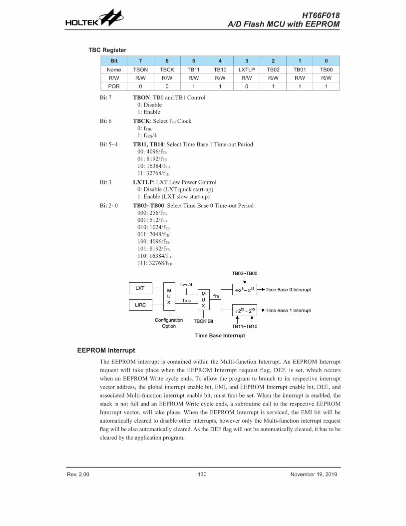
Rev. 2.00 130 November 19, 2019 Rev. 2.00 131 November 19, 2019
HT66F018A/D Flash MCU with EEPROM
HT66F018A/D Flash MCU with EEPROM
TBC RegisterBit 7 6 5 4 3 2 1 0
Name TBON TBCK TB11 TB10 LXTLP TB02 TB01 TB00R/W R/W R/W R/W R/W R/W R/W R/W R/WPOR 0 0 1 1 0 1 1 1
Bit 7 TBON: TB0 and TB1 Control0: Disable1: Enable
Bit 6 TBCK: Select fTB Clock0: fTBC
1: fSYS/4Bit 5~4 TB11, TB10: Select Time Base 1 Time-out Period
00: 4096/fTB
01: 8192/fTB
10: 16384/fTB
11: 32768/fTB Bit 3 LXTLP: LXT Low Power Control
0: Disable (LXT quick start-up)1: Enable (LXT slow start-up)
Bit 2~0 TB02~TB00: Select Time Base 0 Time-out Period000: 256/fTB
001: 512/fTB
010: 1024/fTB
011: 2048/fTB
100: 4096/fTB
101: 8192/fTB
110: 16384/fTB
111: 32768/fTB
Time Base Interrupt
EEPROM InterruptThe EEPROM interrupt is contained within the Multi-function Interrupt. An EEPROM Interrupt request will take place when the EEPROM Interrupt request flag, DEF, is set, which occurs when an EEPROM Write cycle ends. To allow the program to branch to its respective interrupt vector address, the global interrupt enable bit, EMI, and EEPROM Interrupt enable bit, DEE, and associated Multi-function interrupt enable bit, must first be set. When the interrupt is enabled, the stack is not full and an EEPROM Write cycle ends, a subroutine call to the respective EEPROM Interrupt vector, will take place. When the EEPROM Interrupt is serviced, the EMI bit will be automatically cleared to disable other interrupts, however only the Multi-function interrupt request flag will be also automatically cleared. As the DEF flag will not be automatically cleared, it has to be cleared by the application program.
Rev. 2.00 130 November 19, 2019 Rev. 2.00 131 November 19, 2019
HT66F018A/D Flash MCU with EEPROM
HT66F018A/D Flash MCU with EEPROM
LVD Interrupt The Low Voltage Detector Interrupt is contained within the Multi-function Interrupt. A LVD Interrupt request will take place when the LVD Interrupt request flag, LVF, is set, which occurs when the Low Voltage Detector function detects a low power supply voltage. To allow the program to branch to its respective interrupt vector address, the global interrupt enable bit, EMI, Low Voltage Interrupt enable bit, LVE, and associated Multi-function interrupt enable bit, must first be set. When the interrupt is enabled, the stack is not full and a low voltage condition occurs, a subroutine call to the Multi-function Interrupt vector, will take place. When the Low Voltage Interrupt is serviced, the EMI bit will be automatically cleared to disable other interrupts, however only the Multi-function interrupt request flag will be also automatically cleared. As the LVF flag will not be automatically cleared, it has to be cleared by the application program.
TM Interrupts The Compact, Standard and Periodic Type TMs have two interrupts each. All of the TM interrupts are contained within the Multi-function Interrupts. For each of the Compact, Standard and Periodic Type TMs there are two interrupt request flags TnPF and TnAF and two enable bits TnPE and TnAE. A TM interrupt request will take place when any of the TM request flags are set, a situation which occurs when a TM comparator P or A match situation happens.
To allow the program to branch to its respective interrupt vector address, the global interrupt enable bit, EMI, respective TM Interrupt enable bit, and relevant Multi-function Interrupt enable bit, MFnE, must first be set. When the interrupt is enabled, the stack is not full and a TM comparator match situation occurs, a subroutine call to the relevant Multi-function Interrupt vector locations, will take place. When the TM interrupt is serviced, the EMI bit will be automatically cleared to disable other interrupts, however only the related MFnF flag will be automatically cleared. As the TM interrupt request flags will not be automatically cleared, they have to be cleared by the application program.
Interrupt Wake-up FunctionEach of the interrupt functions has the capability of waking up the microcontroller when in the SLEEP or IDLE Mode. A wake-up is generated when an interrupt request flag changes from low to high and is independent of whether the interrupt is enabled or not. Therefore, even though the device is in the SLEEP or IDLE Mode and its system oscillator stopped, situations such as external edge transitions on the external interrupt pins, a low power supply voltage or comparator input change may cause their respective interrupt flag to be set high and consequently generate an interrupt. Care must therefore be taken if spurious wake-up situations are to be avoided. If an interrupt wake-up function is to be disabled then the corresponding interrupt request flag should be set high before the device enters the SLEEP or IDLE Mode. The interrupt enable bits have no effect on the interrupt wake-up function.
Rev. 2.00 132 November 19, 2019 Rev. 2.00 133 November 19, 2019
HT66F018A/D Flash MCU with EEPROM
HT66F018A/D Flash MCU with EEPROM
Programming ConsiderationsBy disabling the relevant interrupt enable bits, a requested interrupt can be prevented from being serviced, however, once an interrupt request flag is set, it will remain in this condition in the interrupt register until the corresponding interrupt is serviced or until the request flag is cleared by the application program.
Where a certain interrupt is contained within a Multi-function interrupt, then when the interrupt service routine is executed, as only the Multi-function interrupt request flags, MFnF, will be automatically cleared, the individual request flag for the function needs to be cleared by the application program.
It is recommended that programs do not use the “CALL” instruction within the interrupt service subroutine. Interrupts often occur in an unpredictable manner or need to be serviced immediately. If only one stack is left and the interrupt is not well controlled, the original control sequence will be damaged once a CALL subroutine is executed in the interrupt subroutine.
Every interrupt has the capability of waking up the microcontroller when it is in SLEEP or IDLE Mode, the wake up being generated when the interrupt request flag changes from low to high. If it is required to prevent a certain interrupt from waking up the microcontroller then its respective request flag should be first set high before enter SLEEP or IDLE Mode.
As only the Program Counter is pushed onto the stack, then when the interrupt is serviced, if the contents of the accumulator, status register or other registers are altered by the interrupt service program, their contents should be saved to the memory at the beginning of the interrupt service routine.
To return from an interrupt subroutine, either a RET or RETI instruction may be executed. The RETI instruction in addition to executing a return to the main program also automatically sets the EMI bit high to allow further interrupts. The RET instruction however only executes a return to the main program leaving the EMI bit in its present zero state and therefore disabling the execution of further interrupts.

Rev. 2.00 132 November 19, 2019 Rev. 2.00 133 November 19, 2019
HT66F018A/D Flash MCU with EEPROM
HT66F018A/D Flash MCU with EEPROM
Low Voltage Detector – LVDEach device has a Low Voltage Detector function, also known as LVD. This enabled the device to monitor the power supply voltage, VDD, and provide a warning signal should it fall below a certain level. This function may be especially useful in battery applications where the supply voltage will gradually reduce as the battery ages, as it allows an early warning battery low signal to be generated. The Low Voltage Detector also has the capability of generating an interrupt signal.
LVD RegisterThe Low Voltage Detector function is controlled using a single register with the name LVDC. Three bits in this register, VLVD2~VLVD0, are used to select one of eight fixed voltages below which a low voltage conditionwill be determined. A low voltage condition is indicatedwhen the LVDO bit is set. If the LVDO bit is low, this indicates that the VDD voltage is above the preset low voltage value. The LVDEN bit is used to control the overall on/off function of the low voltage detector. Setting the bit high will enable the low voltage detector. Clearing the bit to zero will switch off the internal low voltage detector circuits. As the low voltage detector will consume a certain amount of power, it may be desirable to switch off the circuit when not in use, an important consideration in power sensitive battery powered applications.
LVDC RegisterBit 7 6 5 4 3 2 1 0
Name — — LVDO LVDEN — VLVD2 VLVD1 VLVD0R/W — — R R/W — R/W R/W R/WPOR — — 0 0 — 0 0 0
Bit 7~6 Unimplemented, read as "0"Bit 5 LVDO: LVD Output Flag
0: No Low Voltage Detect1: Low Voltage Detect
Bit 4 LVDEN: Low Voltage Detector Control0: Disable1: Enable
Bit 3 Unimplemented, read as “0”Bit 2~0 VLVD2~VLVD0: Select LVD Voltage
000: 2.0V001: 2.2V010: 2.4V011: 2.7V100: 3.0V101: 3.3V110: 3.6V111: 4.0V
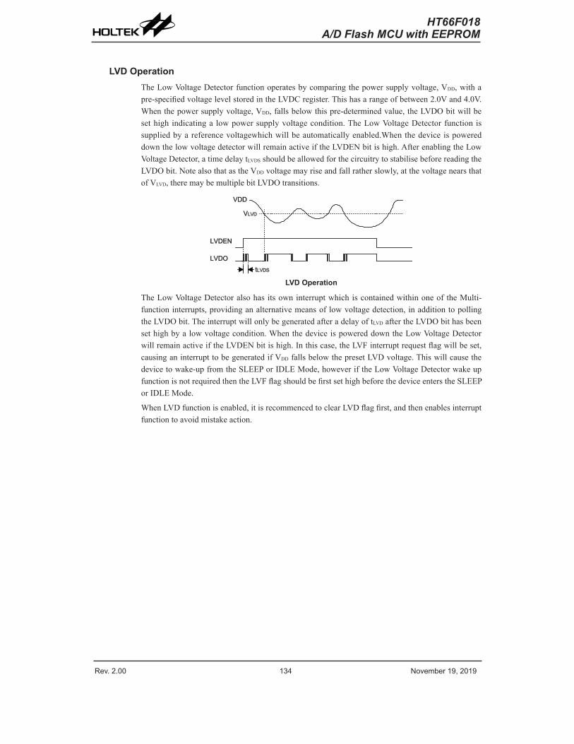
Rev. 2.00 134 November 19, 2019 Rev. 2.00 135 November 19, 2019
HT66F018A/D Flash MCU with EEPROM
HT66F018A/D Flash MCU with EEPROM
LVD OperationThe Low Voltage Detector function operates by comparing the power supply voltage, VDD, with a pre-specified voltage level stored in the LVDC register. This has a range of between 2.0V and 4.0V. When the power supply voltage, VDD, falls below this pre-determined value, the LVDO bit will be set high indicating a low power supply voltage condition. The Low Voltage Detector function is supplied by a reference voltagewhich will be automatically enabled.When the device is powered down the low voltage detector will remain active if the LVDEN bit is high. After enabling the Low Voltage Detector, a time delay tLVDS should be allowed for the circuitry to stabilise before reading the LVDO bit. Note also that as the VDD voltage may rise and fall rather slowly, at the voltage nears that of VLVD, there may be multiple bit LVDO transitions.
LVD Operation
The Low Voltage Detector also has its own interrupt which is contained within one of the Multi-function interrupts, providing an alternative means of low voltage detection, in addition to polling the LVDO bit. The interrupt will only be generated after a delay of tLVD after the LVDO bit has been set high by a low voltage condition. When the device is powered down the Low Voltage Detector will remain active if the LVDEN bit is high. In this case, the LVF interrupt request flag will be set, causing an interrupt to be generated if VDD falls below the preset LVD voltage. This will cause the device to wake-up from the SLEEP or IDLE Mode, however if the Low Voltage Detector wake up function is not required then the LVF flag should be first set high before the device enters the SLEEP or IDLE Mode.
When LVD function is enabled, it is recommenced to clear LVD flag first, and then enables interrupt function to avoid mistake action.
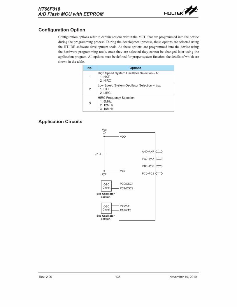
Rev. 2.00 134 November 19, 2019 Rev. 2.00 135 November 19, 2019
HT66F018A/D Flash MCU with EEPROM
HT66F018A/D Flash MCU with EEPROM
Configuration OptionConfiguration options refer to certain options within the MCU that are programmed into the device during the programming process. During the development process, these options are selected using the HT-IDE software development tools. As these options are programmed into the device using the hardware programming tools, once they are selected they cannot be changed later using the application program. All options must be defined for proper system function, the details of which are shown in the table.
No. Options
1High Speed System Oscillator Selection – fH:
1. HXT2. HIRC
2Low Speed System Oscillator Selection – fSUB:
1. LXT2. LIRC
3
HIRC Frequency Selection: 1. 8MHz2. 12MHz3. 16MHz
Application Circuits
� � � � � � � �� � � � � � � �
� � �� � � � � � �
� � � � � � � � � � � � � �� � � � � � �
� � � � � � �
� � � � � � �
� � � � � � �
� � � � � �� � � � � �
� � �� � � � � � �
� � � � � � � � � � � � � �� � � � � � �
�
� � �
� � � �
�
� � � � � � �
Rev. 2.00 136 November 19, 2019 Rev. 2.00 137 November 19, 2019
HT66F018A/D Flash MCU with EEPROM
HT66F018A/D Flash MCU with EEPROM
Instruction Set
IntroductionCentral to the successful operation of any microcontroller is its instruction set, which is a set of program instruction codes that directs the microcontroller to perform certain operations. In the case of Holtek microcontroller, a comprehensive and flexible set of over 60 instructions is provided to enable programmers to implement their application with the minimum of programming overheads.
For easier understanding of the various instruction codes, they have been subdivided into several functional groupings.
Instruction TimingMost instructions are implemented within one instruction cycle. The exceptions to this are branch, call, or table read instructions where two instruction cycles are required. One instruction cycle is equal to 4 system clock cycles, therefore in the case of an 8MHz system oscillator, most instructions would be implemented within 0.5μs and branch or call instructions would be implemented within 1μs. Although instructions which require one more cycle to implement are generally limited to the JMP, CALL, RET, RETI and table read instructions, it is important to realize that any other instructions which involve manipulation of the Program Counter Low register or PCL will also take one more cycle to implement. As instructions which change the contents of the PCL will imply a direct jump to that new address, one more cycle will be required. Examples of such instructions would be “CLR PCL” or “MOV PCL, A”. For the case of skip instructions, it must be noted that if the result of the comparison involves a skip operation then this will also take one more cycle, if no skip is involved then only one cycle is required.
Moving and Transferring DataThe transfer of data within the microcontroller program is one of the most frequently used operations. Making use of three kinds of MOV instructions, data can be transferred from registers to the Accumulator and vice-versa as well as being able to move specific immediate data directly into the Accumulator. One of the most important data transfer applications is to receive data from the input ports and transfer data to the output ports.
Arithmetic OperationsThe ability to perform certain arithmetic operations and data manipulation is a necessary feature of most microcontroller applications. Within the Holtek microcontroller instruction set are a range of add and subtract instruction mnemonics to enable the necessary arithmetic to be carried out. Care must be taken to ensure correct handling of carry and borrow data when results exceed 255 for addition and less than 0 for subtraction. The increment and decrement instructions INC, INCA, DEC and DECA provide a simple means of increasing or decreasing by a value of one of the values in the destination specified.
Rev. 2.00 136 November 19, 2019 Rev. 2.00 137 November 19, 2019
HT66F018A/D Flash MCU with EEPROM
HT66F018A/D Flash MCU with EEPROM
Logical and Rotate OperationThe standard logical operations such as AND, OR, XOR and CPL all have their own instruction within the Holtek microcontroller instruction set. As with the case of most instructions involving data manipulation, data must pass through the Accumulator which may involve additional programming steps. In all logical data operations, the zero flag may be set if the result of the operation is zero. Another form of logical data manipulation comes from the rotate instructions such as RR, RL, RRC and RLC which provide a simple means of rotating one bit right or left. Different rotate instructions exist depending on program requirements. Rotate instructions are useful for serial port programming applications where data can be rotated from an internal register into the Carry bit from where it can be examined and the necessary serial bit set high or low. Another application which rotate data operations are used is to implement multiplication and division calculations.
Branches and Control TransferProgram branching takes the form of either jumps to specified locations using the JMP instruction or to a subroutine using the CALL instruction. They differ in the sense that in the case of a subroutine call, the program must return to the instruction immediately when the subroutine has been carried out. This is done by placing a return instruction “RET” in the subroutine which will cause the program to jump back to the address right after the CALL instruction. In the case of a JMP instruction, the program simply jumps to the desired location. There is no requirement to jump back to the original jumping off point as in the case of the CALL instruction. One special and extremely useful set of branch instructions are the conditional branches. Here a decision is first made regarding the condition of a certain data memory or individual bits. Depending upon the conditions, the program will continue with the next instruction or skip over it and jump to the following instruction. These instructions are the key to decision making and branching within the program perhaps determined by the condition of certain input switches or by the condition of internal data bits.
Bit OperationsThe ability to provide single bit operations on Data Memory is an extremely flexible feature of all Holtek microcontrollers. This feature is especially useful for output port bit programming where individual bits or port pins can be directly set high or low using either the “SET [m].i” or “CLR [m].i” instructions respectively. The feature removes the need for programmers to first read the 8-bit output port, manipulate the input data to ensure that other bits are not changed and then output the port with the correct new data. This read-modify-write process is taken care of automatically when these bit operation instructions are used.
Table Read OperationsData storage is normally implemented by using registers. However, when working with large amounts of fixed data, the volume involved often makes it inconvenient to store the fixed data in the Data Memory. To overcome this problem, Holtek microcontrollers allow an area of Program Memory to be set as a table where data can be directly stored. A set of easy to use instructions provides the means by which this fixed data can be referenced and retrieved from the Program Memory.
Other OperationsIn addition to the above functional instructions, a range of other instructions also exist such as the “HALT” instruction for Power-down operations and instructions to control the operation of the Watchdog Timer for reliable program operations under extreme electric or electromagnetic environments. For their relevant operations, refer to the functional related sections.

Rev. 2.00 138 November 19, 2019 Rev. 2.00 139 November 19, 2019
HT66F018A/D Flash MCU with EEPROM
HT66F018A/D Flash MCU with EEPROM
Instruction Set SummaryThe following table depicts a summary of the instruction set categorised according to function and can be consulted as a basic instruction reference using the following listed conventions.
Table Conventionsx: Bits immediate data m: Data Memory address A: Accumulator i: 0~7 number of bits addr: Program memory address
Mnemonic Description Cycles Flag AffectedArithmeticADD A,[m] Add Data Memory to ACC 1 Z, C, AC, OVADDM A,[m] Add ACC to Data Memory 1Note Z, C, AC, OVADD A,x Add immediate data to ACC 1 Z, C, AC, OVADC A,[m] Add Data Memory to ACC with Carry 1 Z, C, AC, OVADCM A,[m] Add ACC to Data memory with Carry 1Note Z, C, AC, OVSUB A,x Subtract immediate data from the ACC 1 Z, C, AC, OVSUB A,[m] Subtract Data Memory from ACC 1 Z, C, AC, OVSUBM A,[m] Subtract Data Memory from ACC with result in Data Memory 1Note Z, C, AC, OVSBC A,[m] Subtract Data Memory from ACC with Carry 1 Z, C, AC, OVSBCM A,[m] Subtract Data Memory from ACC with Carry, result in Data Memory 1Note Z, C, AC, OVDAA [m] Decimal adjust ACC for Addition with result in Data Memory 1Note CLogic OperationAND A,[m] Logical AND Data Memory to ACC 1 ZOR A,[m] Logical OR Data Memory to ACC 1 ZXOR A,[m] Logical XOR Data Memory to ACC 1 ZANDM A,[m] Logical AND ACC to Data Memory 1Note ZORM A,[m] Logical OR ACC to Data Memory 1Note ZXORM A,[m] Logical XOR ACC to Data Memory 1Note ZAND A,x Logical AND immediate Data to ACC 1 ZOR A,x Logical OR immediate Data to ACC 1 ZXOR A,x Logical XOR immediate Data to ACC 1 ZCPL [m] Complement Data Memory 1Note ZCPLA [m] Complement Data Memory with result in ACC 1 ZIncrement & DecrementINCA [m] Increment Data Memory with result in ACC 1 ZINC [m] Increment Data Memory 1Note ZDECA [m] Decrement Data Memory with result in ACC 1 ZDEC [m] Decrement Data Memory 1Note ZRotateRRA [m] Rotate Data Memory right with result in ACC 1 NoneRR [m] Rotate Data Memory right 1Note NoneRRCA [m] Rotate Data Memory right through Carry with result in ACC 1 CRRC [m] Rotate Data Memory right through Carry 1Note CRLA [m] Rotate Data Memory left with result in ACC 1 NoneRL [m] Rotate Data Memory left 1Note NoneRLCA [m] Rotate Data Memory left through Carry with result in ACC 1 CRLC [m] Rotate Data Memory left through Carry 1Note C
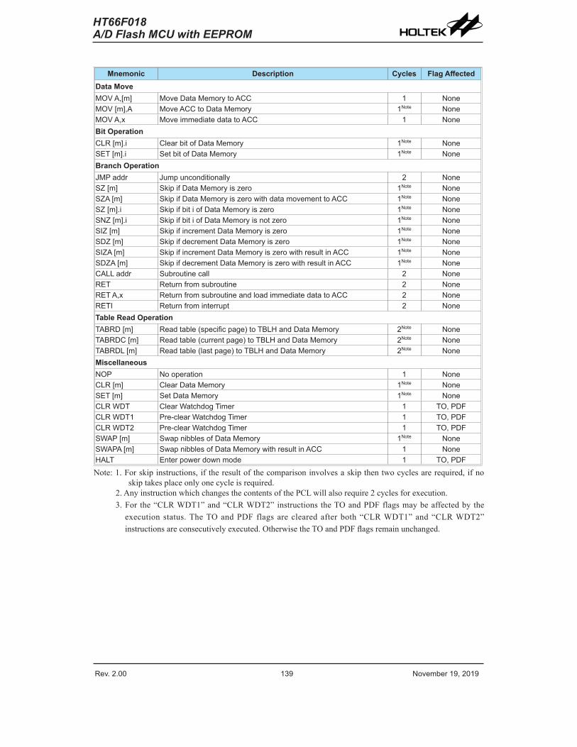
Rev. 2.00 138 November 19, 2019 Rev. 2.00 139 November 19, 2019
HT66F018A/D Flash MCU with EEPROM
HT66F018A/D Flash MCU with EEPROM
Mnemonic Description Cycles Flag AffectedData MoveMOV A,[m] Move Data Memory to ACC 1 NoneMOV [m],A Move ACC to Data Memory 1Note NoneMOV A,x Move immediate data to ACC 1 NoneBit OperationCLR [m].i Clear bit of Data Memory 1Note NoneSET [m].i Set bit of Data Memory 1Note NoneBranch OperationJMP addr Jump unconditionally 2 NoneSZ [m] Skip if Data Memory is zero 1Note NoneSZA [m] Skip if Data Memory is zero with data movement to ACC 1Note NoneSZ [m].i Skip if bit i of Data Memory is zero 1Note NoneSNZ [m].i Skip if bit i of Data Memory is not zero 1Note NoneSIZ [m] Skip if increment Data Memory is zero 1Note NoneSDZ [m] Skip if decrement Data Memory is zero 1Note NoneSIZA [m] Skip if increment Data Memory is zero with result in ACC 1Note NoneSDZA [m] Skip if decrement Data Memory is zero with result in ACC 1Note NoneCALL addr Subroutine call 2 NoneRET Return from subroutine 2 NoneRET A,x Return from subroutine and load immediate data to ACC 2 NoneRETI Return from interrupt 2 NoneTable Read OperationTABRD [m] Read table (specific page) to TBLH and Data Memory 2Note NoneTABRDC [m] Read table (current page) to TBLH and Data Memory 2Note NoneTABRDL [m] Read table (last page) to TBLH and Data Memory 2Note NoneMiscellaneousNOP No operation 1 NoneCLR [m] Clear Data Memory 1Note NoneSET [m] Set Data Memory 1Note NoneCLR WDT Clear Watchdog Timer 1 TO, PDFCLR WDT1 Pre-clear Watchdog Timer 1 TO, PDFCLR WDT2 Pre-clear Watchdog Timer 1 TO, PDFSWAP [m] Swap nibbles of Data Memory 1Note NoneSWAPA [m] Swap nibbles of Data Memory with result in ACC 1 NoneHALT Enter power down mode 1 TO, PDFNote: 1. For skip instructions, if the result of the comparison involves a skip then two cycles are required, if no
skip takes place only one cycle is required.2. Any instruction which changes the contents of the PCL will also require 2 cycles for execution.3. For the “CLR WDT1” and “CLR WDT2” instructions the TO and PDF flags may be affected by the
execution status. The TO and PDF flags are cleared after both “CLR WDT1” and “CLR WDT2” instructions are consecutively executed. Otherwise the TO and PDF flags remain unchanged.
Rev. 2.00 140 November 19, 2019 Rev. 2.00 141 November 19, 2019
HT66F018A/D Flash MCU with EEPROM
HT66F018A/D Flash MCU with EEPROM
Instruction Definition
ADC A,[m] Add Data Memory to ACC with CarryDescription The contents of the specified Data Memory, Accumulator and the carry flag are added. The result is stored in the Accumulator.Operation ACC ← ACC + [m] + CAffected flag(s) OV, Z, AC, C
ADCM A,[m] Add ACC to Data Memory with CarryDescription The contents of the specified Data Memory, Accumulator and the carry flag are added. The result is stored in the specified Data Memory.Operation [m] ← ACC + [m] + CAffected flag(s) OV, Z, AC, C
ADD A,[m] Add Data Memory to ACCDescription The contents of the specified Data Memory and the Accumulator are added. The result is stored in the Accumulator.Operation ACC ← ACC + [m]Affected flag(s) OV, Z, AC, C
ADD A,x Add immediate data to ACCDescription The contents of the Accumulator and the specified immediate data are added. The result is stored in the Accumulator.Operation ACC ← ACC + xAffected flag(s) OV, Z, AC, C
ADDM A,[m] Add ACC to Data MemoryDescription The contents of the specified Data Memory and the Accumulator are added. The result is stored in the specified Data Memory.Operation [m] ← ACC + [m]Affected flag(s) OV, Z, AC, C
AND A,[m] Logical AND Data Memory to ACCDescription Data in the Accumulator and the specified Data Memory perform a bitwise logical AND operation. The result is stored in the Accumulator.Operation ACC ← ACC ″AND″ [m]Affected flag(s) Z
AND A,x Logical AND immediate data to ACCDescription Data in the Accumulator and the specified immediate data perform a bit wise logical AND operation. The result is stored in the Accumulator.Operation ACC ← ACC ″AND″ xAffected flag(s) Z
ANDM A,[m] Logical AND ACC to Data MemoryDescription Data in the specified Data Memory and the Accumulator perform a bitwise logical AND operation. The result is stored in the Data Memory.Operation [m] ← ACC ″AND″ [m]Affected flag(s) Z
Rev. 2.00 140 November 19, 2019 Rev. 2.00 141 November 19, 2019
HT66F018A/D Flash MCU with EEPROM
HT66F018A/D Flash MCU with EEPROM
CALL addr Subroutine callDescription Unconditionally calls a subroutine at the specified address. The Program Counter then increments by 1 to obtain the address of the next instruction which is then pushed onto the stack. The specified address is then loaded and the program continues execution from this new address. As this instruction requires an additional operation, it is a two cycle instruction.Operation Stack ← Program Counter + 1 Program Counter ← addrAffected flag(s) None
CLR [m] Clear Data MemoryDescription Each bit of the specified Data Memory is cleared to 0.Operation [m] ← 00HAffected flag(s) None
CLR [m].i Clear bit of Data MemoryDescription Bit i of the specified Data Memory is cleared to 0.Operation [m].i ← 0Affected flag(s) None
CLR WDT Clear Watchdog TimerDescription The TO, PDF flags and the WDT are all cleared. Operation WDT cleared TO ← 0 PDF ← 0Affected flag(s) TO, PDF
CLR WDT1 Pre-clear Watchdog TimerDescription The TO, PDF flags and the WDT are all cleared. Note that this instruction works in conjunction with CLR WDT2 and must be executed alternately with CLR WDT2 to have effect. Repetitively executing this instruction without alternately executing CLR WDT2 will have no effect.Operation WDT cleared TO ← 0 PDF ← 0 Affected flag(s) TO, PDF
CLR WDT2 Pre-clear Watchdog TimerDescription The TO, PDF flags and the WDT are all cleared. Note that this instruction works in conjunction with CLR WDT1 and must be executed alternately with CLR WDT1 to have effect. Repetitively executing this instruction without alternately executing CLR WDT1 will have no effect.Operation WDT cleared TO ← 0 PDF ← 0Affected flag(s) TO, PDF
CPL [m] Complement Data MemoryDescription Each bit of the specified Data Memory is logically complemented (1′s complement). Bits which previously contained a 1 are changed to 0 and vice versa.Operation [m] ← [m]Affected flag(s) Z
Rev. 2.00 142 November 19, 2019 Rev. 2.00 143 November 19, 2019
HT66F018A/D Flash MCU with EEPROM
HT66F018A/D Flash MCU with EEPROM
CPLA [m] Complement Data Memory with result in ACCDescription Each bit of the specified Data Memory is logically complemented (1′s complement). Bits which previously contained a 1 are changed to 0 and vice versa. The complemented result is stored in the Accumulator and the contents of the Data Memory remain unchanged.Operation ACC ← [m]Affected flag(s) Z
DAA [m] Decimal-Adjust ACC for addition with result in Data MemoryDescription Convert the contents of the Accumulator value to a BCD (Binary Coded Decimal) value resulting from the previous addition of two BCD variables. If the low nibble is greater than 9 or if AC flag is set, then a value of 6 will be added to the low nibble. Otherwise the low nibble remains unchanged. If the high nibble is greater than 9 or if the C flag is set, then a value of 6 will be added to the high nibble. Essentially, the decimal conversion is performed by adding 00H, 06H, 60H or 66H depending on the Accumulator and flag conditions. Only the C flag may be affected by this instruction which indicates that if the original BCD sum is greater than 100, it allows multiple precision decimal addition.Operation [m] ← ACC + 00H or [m] ← ACC + 06H or [m] ← ACC + 60H or [m] ← ACC + 66HAffected flag(s) C
DEC [m] Decrement Data MemoryDescription Data in the specified Data Memory is decremented by 1.Operation [m] ← [m] − 1Affected flag(s) Z
DECA [m] Decrement Data Memory with result in ACCDescription Data in the specified Data Memory is decremented by 1. The result is stored in the Accumulator. The contents of the Data Memory remain unchanged.Operation ACC ← [m] − 1Affected flag(s) Z
HALT Enter power down modeDescription This instruction stops the program execution and turns off the system clock. The contents of the Data Memory and registers are retained. The WDT and prescaler are cleared. The power down flag PDF is set and the WDT time-out flag TO is cleared.Operation TO ← 0 PDF ← 1Affected flag(s) TO, PDF
INC [m] Increment Data Memory Description Data in the specified Data Memory is incremented by 1.Operation [m] ← [m] + 1Affected flag(s) Z
INCA [m] Increment Data Memory with result in ACCDescription Data in the specified Data Memory is incremented by 1. The result is stored in the Accumulator. The contents of the Data Memory remain unchanged.Operation ACC ← [m] + 1Affected flag(s) Z
Rev. 2.00 142 November 19, 2019 Rev. 2.00 143 November 19, 2019
HT66F018A/D Flash MCU with EEPROM
HT66F018A/D Flash MCU with EEPROM
JMP addr Jump unconditionallyDescription The contents of the Program Counter are replaced with the specified address. Program execution then continues from this new address. As this requires the insertion of a dummy instruction while the new address is loaded, it is a two cycle instruction.Operation Program Counter ← addrAffected flag(s) None
MOV A,[m] Move Data Memory to ACCDescription The contents of the specified Data Memory are copied to the Accumulator.Operation ACC ← [m]Affected flag(s) None
MOV A,x Move immediate data to ACCDescription The immediate data specified is loaded into the Accumulator.Operation ACC ← xAffected flag(s) None
MOV [m],A Move ACC to Data Memory Description The contents of the Accumulator are copied to the specified Data Memory.Operation [m] ← ACCAffected flag(s) None
NOP No operationDescription No operation is performed. Execution continues with the next instruction.Operation No operationAffected flag(s) None
OR A,[m] Logical OR Data Memory to ACCDescription Data in the Accumulator and the specified Data Memory perform a bitwise logical OR operation. The result is stored in the Accumulator.Operation ACC ← ACC ″OR″ [m]Affected flag(s) Z
OR A,x Logical OR immediate data to ACCDescription Data in the Accumulator and the specified immediate data perform a bitwise logical OR operation. The result is stored in the Accumulator.Operation ACC ← ACC ″OR″ xAffected flag(s) Z
ORM A,[m] Logical OR ACC to Data MemoryDescription Data in the specified Data Memory and the Accumulator perform a bitwise logical OR operation. The result is stored in the Data Memory.Operation [m] ← ACC ″OR″ [m]Affected flag(s) Z
RET Return from subroutineDescription The Program Counter is restored from the stack. Program execution continues at the restored address.Operation Program Counter ← StackAffected flag(s) None
Rev. 2.00 144 November 19, 2019 Rev. 2.00 145 November 19, 2019
HT66F018A/D Flash MCU with EEPROM
HT66F018A/D Flash MCU with EEPROM
RET A,x Return from subroutine and load immediate data to ACCDescription The Program Counter is restored from the stack and the Accumulator loaded with the specified immediate data. Program execution continues at the restored address.Operation Program Counter ← Stack ACC ← xAffected flag(s) None
RETI Return from interruptDescription The Program Counter is restored from the stack and the interrupts are re-enabled by setting the EMI bit. EMI is the master interrupt global enable bit. If an interrupt was pending when the RETI instruction is executed, the pending Interrupt routine will be processed before returning to the main program.Operation Program Counter ← Stack EMI ← 1Affected flag(s) None
RL [m] Rotate Data Memory leftDescription The contents of the specified Data Memory are rotated left by 1 bit with bit 7 rotated into bit 0.Operation [m].(i+1) ← [m].i; (i=0~6) [m].0 ← [m].7Affected flag(s) None
RLA [m] Rotate Data Memory left with result in ACCDescription The contents of the specified Data Memory are rotated left by 1 bit with bit 7 rotated into bit 0. The rotated result is stored in the Accumulator and the contents of the Data Memory remain unchanged.Operation ACC.(i+1) ← [m].i; (i=0~6) ACC.0 ← [m].7Affected flag(s) None
RLC [m] Rotate Data Memory left through CarryDescription The contents of the specified Data Memory and the carry flag are rotated left by 1 bit. Bit 7 replaces the Carry bit and the original carry flag is rotated into bit 0.Operation [m].(i+1) ← [m].i; (i=0~6) [m].0 ← C C ← [m].7Affected flag(s) C
RLCA [m] Rotate Data Memory left through Carry with result in ACCDescription Data in the specified Data Memory and the carry flag are rotated left by 1 bit. Bit 7 replaces the Carry bit and the original carry flag is rotated into the bit 0. The rotated result is stored in the Accumulator and the contents of the Data Memory remain unchanged.Operation ACC.(i+1) ← [m].i; (i=0~6) ACC.0 ← C C ← [m].7Affected flag(s) C
RR [m] Rotate Data Memory rightDescription The contents of the specified Data Memory are rotated right by 1 bit with bit 0 rotated into bit 7.Operation [m].i ← [m].(i+1); (i=0~6) [m].7 ← [m].0Affected flag(s) None
Rev. 2.00 144 November 19, 2019 Rev. 2.00 145 November 19, 2019
HT66F018A/D Flash MCU with EEPROM
HT66F018A/D Flash MCU with EEPROM
RRA [m] Rotate Data Memory right with result in ACCDescription Data in the specified Data Memory and the carry flag are rotated right by 1 bit with bit 0 rotated into bit 7. The rotated result is stored in the Accumulator and the contents of the Data Memory remain unchanged.Operation ACC.i ← [m].(i+1); (i=0~6) ACC.7 ← [m].0Affected flag(s) None
RRC [m] Rotate Data Memory right through CarryDescription The contents of the specified Data Memory and the carry flag are rotated right by 1 bit. Bit 0 replaces the Carry bit and the original carry flag is rotated into bit 7.Operation [m].i ← [m].(i+1); (i=0~6) [m].7 ← C C ← [m].0Affected flag(s) C
RRCA [m] Rotate Data Memory right through Carry with result in ACCDescription Data in the specified Data Memory and the carry flag are rotated right by 1 bit. Bit 0 replaces the Carry bit and the original carry flag is rotated into bit 7. The rotated result is stored in the Accumulator and the contents of the Data Memory remain unchanged.Operation ACC.i ← [m].(i+1); (i=0~6) ACC.7 ← C C ← [m].0Affected flag(s) C
SBC A,[m] Subtract Data Memory from ACC with CarryDescription The contents of the specified Data Memory and the complement of the carry flag are subtracted from the Accumulator. The result is stored in the Accumulator. Note that if the result of subtraction is negative, the C flag will be cleared to 0, otherwise if the result is positive or zero, the C flag will be set to 1.Operation ACC ← ACC − [m] − CAffected flag(s) OV, Z, AC, C
SBCM A,[m] Subtract Data Memory from ACC with Carry and result in Data MemoryDescription The contents of the specified Data Memory and the complement of the carry flag are subtracted from the Accumulator. The result is stored in the Data Memory. Note that if the result of subtraction is negative, the C flag will be cleared to 0, otherwise if the result is positive or zero, the C flag will be set to 1.Operation [m] ← ACC − [m] − CAffected flag(s) OV, Z, AC, C
SDZ [m] Skip if decrement Data Memory is 0Description The contents of the specified Data Memory are first decremented by 1. If the result is 0 the following instruction is skipped. As this requires the insertion of a dummy instruction while the next instruction is fetched, it is a two cycle instruction. If the result is not 0 the program proceeds with the following instruction.Operation [m] ← [m] − 1 Skip if [m]=0Affected flag(s) None
Rev. 2.00 146 November 19, 2019 Rev. 2.00 147 November 19, 2019
HT66F018A/D Flash MCU with EEPROM
HT66F018A/D Flash MCU with EEPROM
SDZA [m] Skip if decrement Data Memory is zero with result in ACCDescription The contents of the specified Data Memory are first decremented by 1. If the result is 0, the following instruction is skipped. The result is stored in the Accumulator but the specified Data Memory contents remain unchanged. As this requires the insertion of a dummy instruction while the next instruction is fetched, it is a two cycle instruction. If the result is not 0, the program proceeds with the following instruction.Operation ACC ← [m] − 1 Skip if ACC=0Affected flag(s) None
SET [m] Set Data MemoryDescription Each bit of the specified Data Memory is set to 1.Operation [m] ← FFHAffected flag(s) None
SET [m].i Set bit of Data MemoryDescription Bit i of the specified Data Memory is set to 1.Operation [m].i ← 1Affected flag(s) None
SIZ [m] Skip if increment Data Memory is 0Description The contents of the specified Data Memory are first incremented by 1. If the result is 0, the following instruction is skipped. As this requires the insertion of a dummy instruction while the next instruction is fetched, it is a two cycle instruction. If the result is not 0 the program proceeds with the following instruction.Operation [m] ← [m] + 1 Skip if [m]=0 Affected flag(s) None
SIZA [m] Skip if increment Data Memory is zero with result in ACCDescription The contents of the specified Data Memory are first incremented by 1. If the result is 0, the following instruction is skipped. The result is stored in the Accumulator but the specified Data Memory contents remain unchanged. As this requires the insertion of a dummy instruction while the next instruction is fetched, it is a two cycle instruction. If the result is not 0 the program proceeds with the following instruction.Operation ACC ← [m] + 1 Skip if ACC=0Affected flag(s) None
SNZ [m].i Skip if bit i of Data Memory is not 0Description If bit i of the specified Data Memory is not 0, the following instruction is skipped. As this requires the insertion of a dummy instruction while the next instruction is fetched, it is a two cycle instruction. If the result is 0 the program proceeds with the following instruction.Operation Skip if [m].i ≠ 0Affected flag(s) None
SUB A,[m] Subtract Data Memory from ACCDescription The specified Data Memory is subtracted from the contents of the Accumulator. The result is stored in the Accumulator. Note that if the result of subtraction is negative, the C flag will be cleared to 0, otherwise if the result is positive or zero, the C flag will be set to 1.Operation ACC ← ACC − [m]Affected flag(s) OV, Z, AC, C
Rev. 2.00 146 November 19, 2019 Rev. 2.00 147 November 19, 2019
HT66F018A/D Flash MCU with EEPROM
HT66F018A/D Flash MCU with EEPROM
SUBM A,[m] Subtract Data Memory from ACC with result in Data MemoryDescription The specified Data Memory is subtracted from the contents of the Accumulator. The result is stored in the Data Memory. Note that if the result of subtraction is negative, the C flag will be cleared to 0, otherwise if the result is positive or zero, the C flag will be set to 1.Operation [m] ← ACC − [m]Affected flag(s) OV, Z, AC, C
SUB A,x Subtract immediate data from ACCDescription The immediate data specified by the code is subtracted from the contents of the Accumulator. The result is stored in the Accumulator. Note that if the result of subtraction is negative, the C flag will be cleared to 0, otherwise if the result is positive or zero, the C flag will be set to 1.Operation ACC ← ACC − xAffected flag(s) OV, Z, AC, C
SWAP [m] Swap nibbles of Data MemoryDescription The low-order and high-order nibbles of the specified Data Memory are interchanged.Operation [m].3~[m].0 ↔ [m].7~[m].4Affected flag(s) None
SWAPA [m] Swap nibbles of Data Memory with result in ACCDescription The low-order and high-order nibbles of the specified Data Memory are interchanged. The result is stored in the Accumulator. The contents of the Data Memory remain unchanged.Operation ACC.3~ACC.0 ← [m].7~[m].4 ACC.7~ACC.4 ← [m].3~[m].0Affected flag(s) None
SZ [m] Skip if Data Memory is 0Description If the contents of the specified Data Memory is 0, the following instruction is skipped. As this requires the insertion of a dummy instruction while the next instruction is fetched, it is a two cycle instruction. If the result is not 0 the program proceeds with the following instruction.Operation Skip if [m]=0Affected flag(s) None
SZA [m] Skip if Data Memory is 0 with data movement to ACCDescription The contents of the specified Data Memory are copied to the Accumulator. If the value is zero, the following instruction is skipped. As this requires the insertion of a dummy instruction while the next instruction is fetched, it is a two cycle instruction. If the result is not 0 the program proceeds with the following instruction.Operation ACC ← [m] Skip if [m]=0Affected flag(s) None
SZ [m].i Skip if bit i of Data Memory is 0Description If bit i of the specified Data Memory is 0, the following instruction is skipped. As this requires the insertion of a dummy instruction while the next instruction is fetched, it is a two cycle instruction. If the result is not 0, the program proceeds with the following instruction.Operation Skip if [m].i=0Affected flag(s) None

Rev. 2.00 148 November 19, 2019 Rev. 2.00 149 November 19, 2019
HT66F018A/D Flash MCU with EEPROM
HT66F018A/D Flash MCU with EEPROM
TABRD [m] Read table (specific page) to TBLH and Data MemoryDescription The low byte of the program code (specific page) addressed by the table pointer pair (TBHP and TBLP) is moved to the specified Data Memory and the high byte moved to TBLH.Operation [m] ← program code (low byte) TBLH ← program code (high byte)Affected flag(s) None
TABRDC [m] Read table (current page) to TBLH and Data MemoryDescription The low byte of the program code (current page) addressed by the table pointer (TBLP) is moved to the specified Data Memory and the high byte moved to TBLH.Operation [m] ← program code (low byte) TBLH ← program code (high byte)Affected flag(s) None
TABRDL [m] Read table (last page) to TBLH and Data MemoryDescription The low byte of the program code (last page) addressed by the table pointer (TBLP) is moved to the specified Data Memory and the high byte moved to TBLH.Operation [m] ← program code (low byte) TBLH ← program code (high byte)Affected flag(s) None
XOR A,[m] Logical XOR Data Memory to ACCDescription Data in the Accumulator and the specified Data Memory perform a bitwise logical XOR operation. The result is stored in the Accumulator.Operation ACC ← ACC ″XOR″ [m]Affected flag(s) Z
XORM A,[m] Logical XOR ACC to Data MemoryDescription Data in the specified Data Memory and the Accumulator perform a bitwise logical XOR operation. The result is stored in the Data Memory.Operation [m] ← ACC ″XOR″ [m]Affected flag(s) Z
XOR A,x Logical XOR immediate data to ACCDescription Data in the Accumulator and the specified immediate data perform a bitwise logical XOR operation. The result is stored in the Accumulator.Operation ACC ← ACC ″XOR″ xAffected flag(s) Z
Rev. 2.00 148 November 19, 2019 Rev. 2.00 149 November 19, 2019
HT66F018A/D Flash MCU with EEPROM
HT66F018A/D Flash MCU with EEPROM
Package Information
Note that the package information provided here is for consultation purposes only. As this information may be updated at regular intervals users are reminded to consult the Holtek website for the latest version of the Package/Carton Information.
Additional supplementary information with regard to packaging is listed below. Click on the relevant section to be transferred to the relevant website page.
• Package Information (include Outline Dimensions, Product Tape and Reel Specifications)
• The Operation Instruction of Packing Materials
• Carton information
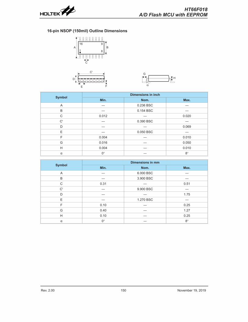
Rev. 2.00 150 November 19, 2019 Rev. 2.00 151 November 19, 2019
HT66F018A/D Flash MCU with EEPROM
HT66F018A/D Flash MCU with EEPROM
16-pin NSOP (150mil) Outline Dimensions
� �
�
�
�
�
� �
�
�
� �
��
� �
SymbolDimensions in inch
Min. Nom. Max.A — 0.236 BSC —B — 0.154 BSC —C 0.012 — 0.020 C' — 0.390 BSC —D — — 0.069 E — 0.050 BSC —F 0.004 — 0.010 G 0.016 — 0.050 H 0.004 — 0.010 α 0° ― 8°
SymbolDimensions in mm
Min. Nom. Max.A — 6.000 BSC —B — 3.900 BSC —C 0.31 — 0.51 C' — 9.900 BSC —D — — 1.75 E — 1.270 BSC —F 0.10 — 0.25 G 0.40 — 1.27 H 0.10 — 0.25 α 0° ― 8°
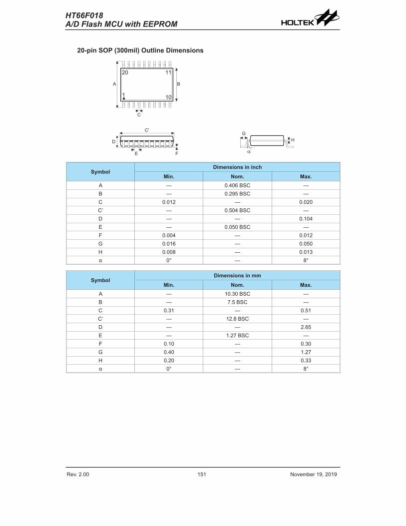
Rev. 2.00 150 November 19, 2019 Rev. 2.00 151 November 19, 2019
HT66F018A/D Flash MCU with EEPROM
HT66F018A/D Flash MCU with EEPROM
20-pin SOP (300mil) Outline Dimensions
� �
�
� �
� �
� �
�
�
� �
� ��
�
�
SymbolDimensions in inch
Min. Nom. Max.A — 0.406 BSC —B — 0.295 BSC —C 0.012 — 0.020 C’ — 0.504 BSC —D — — 0.104 E — 0.050 BSC —F 0.004 — 0.012 G 0.016 — 0.050 H 0.008 — 0.013 α 0° — 8°
SymbolDimensions in mm
Min. Nom. Max.A — 10.30 BSC —B — 7.5 BSC —C 0.31 — 0.51 C’ — 12.8 BSC —D — — 2.65 E — 1.27 BSC —F 0.10 — 0.30 G 0.40 — 1.27 H 0.20 — 0.33 α 0° — 8°

Rev. 2.00 152 November 19, 2019 Rev. 2.00 153 November 19, 2019
HT66F018A/D Flash MCU with EEPROM
HT66F018A/D Flash MCU with EEPROM
20-pin NSOP (150mil) Outline Dimensions
� �
�
� �
� �
� �
�
�
� �
� ��
�
�
SymbolDimensions in inch
Min. Nom. Max.A 0.228 0.236 0.244 B 0.146 0.154 0.161 C 0.009 — 0.012 C’ 0.382 0.390 0.398 D — — 0.069 E — 0.032 BSC —F 0.002 — 0.009 G 0.020 — 0.031 H 0.008 — 0.010 α 0° — 8°
SymbolDimensions in mm
Min. Nom. Max.A 5.80 6.00 6.20 B 3.70 3.90 4.10 C 0.23 — 0.30 C’ 9.70 9.90 10.10 D — — 1.75 E — 0.80 BSC —F 0.05 — 0.23 G 0.50 — 0.80 H 0.21 — 0.25 α 0° — 8°

Rev. 2.00 152 November 19, 2019 Rev. 2.00 153 November 19, 2019
HT66F018A/D Flash MCU with EEPROM
HT66F018A/D Flash MCU with EEPROM
20-pin SSOP (150mil) Outline Dimensions
� �
�
� �
� �
� �
�
�
� �
� � ��
�
SymbolDimensions in inch
Min. Nom. Max.A — 0.236 BSC —B — 0.155 BSC —C 0.008 — 0.012 C’ — 0.341 BSC —D — — 0.069 E — 0.025 BSC —F 0.004 — 0.0098 G 0.016 — 0.05 H 0.004 — 0.01 α 0° — 8°
SymbolDimensions in mm
Min. Nom. Max.A — 6 BSC —B — 3.9 BSC —C 0.20 — 0.30 C’ — 8.66 BSC —D — — 1.75 E — 0.635 BSC —F 0.10 — 0.25 G 0.41 — 1.27 H 0.10 — 0.25 α 0° — 8°
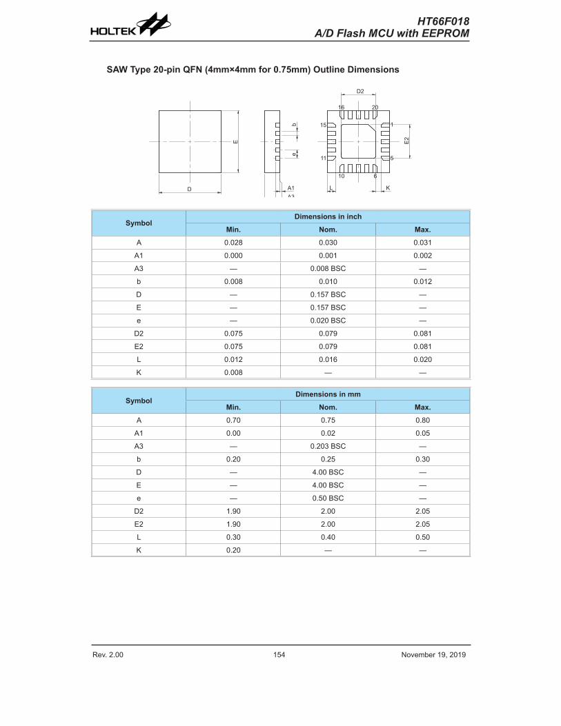
Rev. 2.00 154 November 19, 2019 Rev. 2.00 155 November 19, 2019
HT66F018A/D Flash MCU with EEPROM
HT66F018A/D Flash MCU with EEPROM
SAW Type 20-pin QFN (4mm×4mm for 0.75mm) Outline Dimensions
E
D A1A3
A
L
10 6
K
5
1
20
D2
16
15
11
e
E2
b
SymbolDimensions in inch
Min. Nom. Max.A 0.028 0.030 0.031
A1 0.000 0.001 0.002
A3 — 0.008 BSC —
b 0.008 0.010 0.012
D — 0.157 BSC —
E — 0.157 BSC —
e — 0.020 BSC —
D2 0.075 0.079 0.081
E2 0.075 0.079 0.081
L 0.012 0.016 0.020
K 0.008 — —
SymbolDimensions in mm
Min. Nom. Max.A 0.70 0.75 0.80
A1 0.00 0.02 0.05
A3 — 0.203 BSC —
b 0.20 0.25 0.30
D — 4.00 BSC —
E — 4.00 BSC —
e — 0.50 BSC —
D2 1.90 2.00 2.05
E2 1.90 2.00 2.05
L 0.30 0.40 0.50
K 0.20 — —
Rev. 2.00 154 November 19, 2019 Rev. 2.00 155 November 19, 2019
HT66F018A/D Flash MCU with EEPROM
HT66F018A/D Flash MCU with EEPROM
Copyright© 2019 by HOLTEK SEMICONDUCTOR INC.
The information appearing in this Data Sheet is believed to be accurate at the time of publication. However, Holtek assumes no responsibility arising from the use of the specifications described. The applications mentioned herein are used solely for the purpose of illustration and Holtek makes no warranty or representation that such applications will be suitable without further modification, nor recommends the use of its products for application that may present a risk to human life due to malfunction or otherwise. Holtek's products are not authorized for use as critical components in life support devices or systems. Holtek reserves the right to alter its products without prior notification. For the most up-to-date information, please visit our web site at http://www.holtek.com.


