PIN CONFIGURATIONS 44-Pin Package 28-Pin DIP Package REV. Information furnished by Analog Devices is believed to be accurate and reliable. However, no responsibility is assumed by Analog Devices for its use, nor for any infringements of patents or other rights of third parties which may result from its use. No license is granted by implication or otherwise under any patent or patent rights of Analog Devices. a Monolithic 12-Bit Quad DAC AD664 FEATURES Four Complete Voltage Output DACs Data Register Readback Feature “Reset to Zero” Override Multiplying Operation Double-Buffered Latches Surface Mount and DIP Packages MIL-STD-883 Compliant Versions Available APPLICATIONS Automatic Test Equipment Robotics Process Control Disk Drives Instrumentation Avionics One Technology Way, P.O. Box 9106, Norwood, MA 02062-9106, U.S.A. Tel: Fax: PRODUCT DESCRIPTION The AD664 is four complete 12-bit, voltage-output DACs on one monolithic IC chip. Each DAC has a double-buffered input latch structure and a data readback function. All DAC read and write operations occur through a single microprocessor-compatible I/O port. The I/O port accommodates 4-, 8- or 12-bit parallel words al- lowing simple interfacing with a wide variety of microprocessors. A reset to zero control pin is provided to allow a user to simulta- neously reset all DAC outputs to zero, regardless of the contents of the input latch. Any one or all of the DACs may be placed in a transparent mode allowing immediate response by the outputs to the input data. The analog portion of the AD664 consists of four DAC cells, four output amplifiers, a control amplifier and switches. Each DAC cell is an inverting R-2R type. The output current from each DAC is switched to the on-board application resistors and output amplifier. The output range of each DAC cell is pro- grammed through the digital I/O port and may be set to unipo- lar or bipolar range, with a gain of one or two times the reference voltage. All DACs are operated from a single external reference. The functional completeness of the AD664 results from the combination of Analog Devices’ BiMOS II process, laser-trimmed thin-film resistors and double-level metal interconnects. PRODUCT HIGHLIGHTS 1. The AD664 provides four voltage-output DACs on one chip offering the highest density 12-bit D/A function available. 2. The output range of each DAC is fully and independently programmable. 3. Readback capability allows verification of contents of the in- ternal data registers. 4. The asynchronous RESET control returns all D/A outputs to zero volts. 5. DAC-to-DAC matching performance is specified and tested. 6. Linearity error is specified to be 1/2 LSB at room tempera- ture and 3/4 LSB maximum for the K, B and T grades. 7. DAC performance is guaranteed to be monotonic over the full operating temperature range. 8. Readback buffers have tristate outputs. 9. Multiplying-mode operation allows use with fixed or vari- able, positive or negative external references. 10. The AD664 is available in versions compliant with MIL- STD-883. Refer to the Analog Devices Military Products Databook or current AD664/883B data sheet for detailed specifications. 781/329-4700 781/461-3113 D
Transcript
PIN CONFIGURATIONS
44-Pin Package
28-Pin DIP Package
REV.
Information furnished by Analog Devices is believed to be accurate andreliable. However, no responsibility is assumed by Analog Devices for itsuse, nor for any infringements of patents or other rights of third partieswhich may result from its use. No license is granted by implication orotherwise under any patent or patent rights of Analog Devices.
a Monolithic12-Bit Quad DAC
AD664FEATURES
Four Complete Voltage Output DACs
Data Register Readback Feature
“Reset to Zero” Override
Multiplying Operation
Double-Buffered Latches
Surface Mount and DIP Packages
MIL-STD-883 Compliant Versions Available
APPLICATIONS
Automatic Test Equipment
Robotics
Process Control
Disk Drives
Instrumentation
Avionics
One Technology Way, P.O. Box 9106, Norwood, MA 02062-9106, U.S.A.
Tel: Fax:
PRODUCT DESCRIPTIONThe AD664 is four complete 12-bit, voltage-output DACs onone monolithic IC chip. Each DAC has a double-buffered inputlatch structure and a data readback function. All DAC read andwrite operations occur through a single microprocessor-compatibleI/O port.
The I/O port accommodates 4-, 8- or 12-bit parallel words al-lowing simple interfacing with a wide variety of microprocessors.A reset to zero control pin is provided to allow a user to simulta-neously reset all DAC outputs to zero, regardless of the contentsof the input latch. Any one or all of the DACs may be placed ina transparent mode allowing immediate response by the outputsto the input data.
The analog portion of the AD664 consists of four DAC cells,four output amplifiers, a control amplifier and switches. EachDAC cell is an inverting R-2R type. The output current fromeach DAC is switched to the on-board application resistors andoutput amplifier. The output range of each DAC cell is pro-grammed through the digital I/O port and may be set to unipo-lar or bipolar range, with a gain of one or two times the referencevoltage. All DACs are operated from a single external reference.
The functional completeness of the AD664 results from thecombination of Analog Devices’ BiMOS II process, laser-trimmedthin-film resistors and double-level metal interconnects.
PRODUCT HIGHLIGHTS1. The AD664 provides four voltage-output DACs on one chip
offering the highest density 12-bit D/A function available.
2. The output range of each DAC is fully and independentlyprogrammable.
3. Readback capability allows verification of contents of the in-ternal data registers.
4. The asynchronous RESET control returns all D/A outputsto zero volts.
5. DAC-to-DAC matching performance is specified and tested.
6. Linearity error is specified to be 1/2 LSB at room tempera-ture and 3/4 LSB maximum for the K, B and T grades.
7. DAC performance is guaranteed to be monotonic over thefull operating temperature range.
8. Readback buffers have tristate outputs.
9. Multiplying-mode operation allows use with fixed or vari-able, positive or negative external references.
10. The AD664 is available in versions compliant with MIL-STD-883. Refer to the Analog Devices Military ProductsDatabook or current AD664/883B data sheet for detailedspecifications.
Unipolar 0 V to +10 V Mode –12 ±7 12 –10 ±5 10 ppm of FSR5/°CBipolar –5 V to +5 V Mode –12 ±7 12 –10 ±5 10 ppm of FSR/°CBipolar –10 V to +10 V Mode –12 ±7 12 –10 ±5 10 ppm of FSR/°C
Unipolar Offset DriftUnipolar 0 V to +10 V Mode –3 ± l.5 3 –2 ± l 2 ppm of FSR/°C
Bipolar Zero DriftBipolar –5 V to +5 V Mode –12 ±7 12 –10 ±5 10 ppm of FSR/°CBipolar –10 V to +10 V Mode –12 ±7 12 –10 ±5 10 ppm of FSR/°C
DIGITAL OUTPUTSVOL @ 1.6 mA Sink 0.4 * VoltsVOH @ 0.5 mA Source 2.4 * Volts
TEMPERATURE RANGEJN/JP/KN/KP 0 +70 * * °CAD/AJ/BD/BJ/BE – 40 +85 * * °CSD/TD/TE –55 +125 * * °C
NOTES 1A minimum power supply of ±12.0 V is required for 0 V to +10 V and ±10 V operation. A minimum power supply of ±11.4 V is required for –5 V to +5 V operation. 2For VCC < +12 V and VEE > –12 V. Voltage not to exeeed 10 V maximum. 3Bipolar zero error is the difference from the ideal output (0 volts) and the actual output voltage with code 100 000 000 000 applied to the inputs. 4Linearity error is defined as the maximum deviation of the actual DAC output from the ideal output (a straight line drawn from 0 to F.S. – 1 LSB). 5FSR means Full-Scale Range and is 20 V for ±10 V range and 10 V for ± 5 V range. 6A minimum power supply of ±12.0 V is required for a 10 V reference voltage. 7Analog Ground Current is input code dependent. 8Gain error matching is the largest difference in gain error between any two DACs in one package. 9Offset error matching is the largest difference in offset error between any two DACs in one package.10Bipolar zero error matching is the largest difference in bipolar zero error between any two DACs in one package.11Linearity error matching is the difference in the worst ease linearity error between any two DACs in one package.1244-pin versions only.*Specifications same as JN/JP/AD/AJ/SD.Specifications subject to change without notice.Specifications shown in boldface are tested on all production units at final electrical test. Results from those tests are used to calculate outgoing quality levels. All minand max specifications are guaranteed, although only those shown in boldface are tested on all production units.
≤ (VCC – 2 V, VEE + 2 V)VCC to VEE . . . . . . . . . . . . . . . . . . . . . . . . . . . . . . . 0 to +36 V
CAUTIONESD (electrostatic discharge) sensitive device. Unused devices must be stored in conductive foamor shunts. The protective foam should be discharged to the destination socket before devices areremoved.
*Stresses above those listed under “Absolute Maximum Ratings” may causepermanent damage to the device. This is a stress rating only and functionaloperation of the device at these or any other conditions above those indicated in theoperational section of this specification is not implied. Exposure to absolutemaximum rating conditions for extended periods may affect device reliability.
REV. –3–D
AD664
REV. –4–
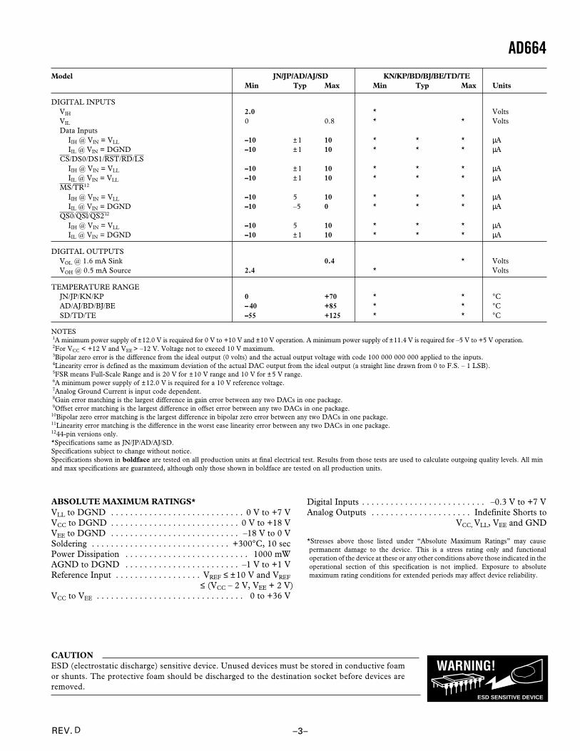
Figure 1a. 44-Pin Block Diagram
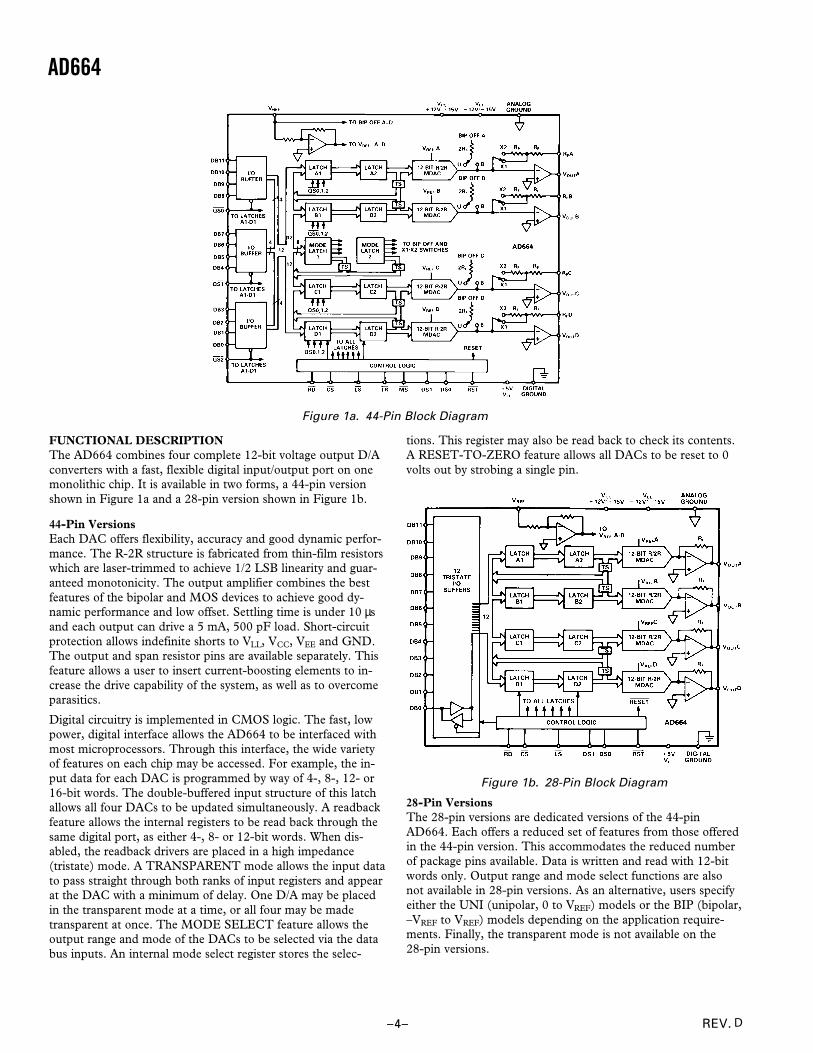
FUNCTIONAL DESCRIPTIONThe AD664 combines four complete 12-bit voltage output D/Aconverters with a fast, flexible digital input/output port on onemonolithic chip. It is available in two forms, a 44-pin versionshown in Figure 1a and a 28-pin version shown in Figure 1b.
44-Pin VersionsEach DAC offers flexibility, accuracy and good dynamic perfor-mance. The R-2R structure is fabricated from thin-film resistorswhich are laser-trimmed to achieve 1/2 LSB linearity and guar-anteed monotonicity. The output amplifier combines the bestfeatures of the bipolar and MOS devices to achieve good dy-namic performance and low offset. Settling time is under 10 µsand each output can drive a 5 mA, 500 pF load. Short-circuitprotection allows indefinite shorts to VLL, VCC, VEE and GND.The output and span resistor pins are available separately. Thisfeature allows a user to insert current-boosting elements to in-crease the drive capability of the system, as well as to overcomeparasitics.
Digital circuitry is implemented in CMOS logic. The fast, lowpower, digital interface allows the AD664 to be interfaced withmost microprocessors. Through this interface, the wide varietyof features on each chip may be accessed. For example, the in-put data for each DAC is programmed by way of 4-, 8-, 12- or16-bit words. The double-buffered input structure of this latchallows all four DACs to be updated simultaneously. A readbackfeature allows the internal registers to be read back through thesame digital port, as either 4-, 8- or 12-bit words. When dis-abled, the readback drivers are placed in a high impedance(tristate) mode. A TRANSPARENT mode allows the input datato pass straight through both ranks of input registers and appearat the DAC with a minimum of delay. One D/A may be placedin the transparent mode at a time, or all four may be madetransparent at once. The MODE SELECT feature allows theoutput range and mode of the DACs to be selected via the databus inputs. An internal mode select register stores the selec-
tions. This register may also be read back to check its contents.A RESET-TO-ZERO feature allows all DACs to be reset to 0volts out by strobing a single pin.
Figure 1b. 28-Pin Block Diagram
28-Pin VersionsThe 28-pin versions are dedicated versions of the 44-pinAD664. Each offers a reduced set of features from those offeredin the 44-pin version. This accommodates the reduced numberof package pins available. Data is written and read with 12-bitwords only. Output range and mode select functions are alsonot available in 28-pin versions. As an alternative, users specifyeither the UNI (unipolar, 0 to VREF) models or the BIP (bipolar,–VREF to VREF) models depending on the application require-ments. Finally, the transparent mode is not available on the28-pin versions.
D
AD664
REV. –5–
Table I. Transfer Functions
Mode = UNI Mode = BIP
000000000000 = 0 V 000000000000 = – VREF/2Gain = 1 100000000000 = VREF/2 100000000000 = 0 V
DEFINITIONS OF SPECIFICATIONSLINEARITY ERROR: Analog Devices defines linearity error asthe maximum deviation of the actual, adjusted DAC outputfrom the ideal analog output (a straight line drawn from 0 to FS– 1 LSB) for any bit combination. This is also referred to asrelative accuracy. The AD664 is laser-trimmed to typicallymaintain linearity errors at less than ±1/4 LSB.
MONOTONICITY: A DAC is said to be monotonic if the out-put either increases or remains constant for increasing digitalinputs such that the output will always be a nondecreasing func-tion of input. All versions of the AD664 are monotonic overtheir full operating temperature range.
DIFFERENTIAL LINEARITY: Monotonic behavior requiresthat the differential linearity error be less than 1 LSB both at25°C as well as over the temperature range of interest. Differen-tial nonlinearity is the measure of the variation in analog value,normalized to full scale, associated with a 1 LSB change in digi-tal input code. For example, for a 10 V full-scale output, achange of 1 LSB in digital input code should result in a2.44 mV change in the analog output (VREF = 10 V, Gain = 1,1 LSB = 10 V × 1/4096 = 2.44 mV). If in actual use, however, a1 LSB change in the input code results in a change of only0.61 mV (1/4 LSB) in analog output, the differential non-linearity error would be –1.83 mV, or –3/4 LSB.
GAIN ERROR: DAC gain error is a measure of the differencebetween the output span of an ideal DAC and an actual device.
UNIPOLAR OFFSET ERROR: Unipolar offset error is the dif-ference between the ideal output (0 V) and the actual output ofa DAC when the input is loaded with all “0s” and the MODE isunipolar.
BIPOLAR ZERO ERROR: Bipolar zero error is the differencebetween the ideal output (0 V) and the actual output of a DACwhen the input code is loaded with the MSB = “1” and the restof the bits = “0” and the MODE is bipolar.
SETTLING TIME: Settling time is the time required for theoutput to reach and remain within a specified error band aboutits final value, measured from the digital input transition.
CROSSTALK: Crosstalk is the change in an output caused bya change in one or more of the other outputs. It is due tocapacitive and thermal coupling between outputs.
REFERENCE FEEDTHROUGH: The portion of an ac refer-ence signal that appears at an output when all input bits are low.Feedthrough is due to capacitive coupling between the referenceinput and the output. It is specified in decibels at a particularfrequency.
REFERENCE 3 dB BANDWIDTH: The frequency of the acreference input signal at which the amplitude of the full-scaleoutput response falls 3 dB from the ideal response.
GLITCH IMPULSE: Glitch impulse is an undesired outputvoltage transient caused by asymmetrical switching times in theswitches of a DAC. These transients are specified by their netarea (in nV-sec) of the voltage vs. time characteristic.
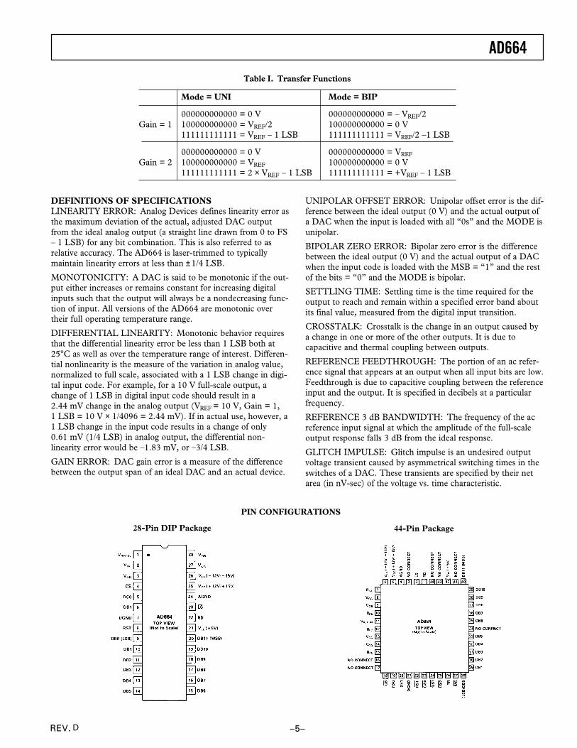
PIN CONFIGURATIONS
28-Pin DIP Package 44-Pin Package
D
AD664
REV. –6–
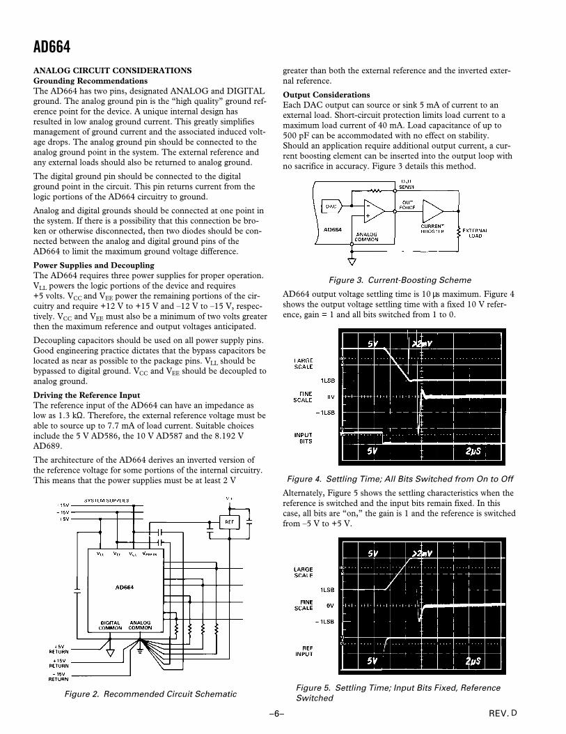
ANALOG CIRCUIT CONSIDERATIONSGrounding RecommendationsThe AD664 has two pins, designated ANALOG and DIGITALground. The analog ground pin is the “high quality” ground ref-erence point for the device. A unique internal design hasresulted in low analog ground current. This greatly simplifiesmanagement of ground current and the associated induced volt-age drops. The analog ground pin should be connected to theanalog ground point in the system. The external reference andany external loads should also be returned to analog ground.
The digital ground pin should be connected to the digitalground point in the circuit. This pin returns current from thelogic portions of the AD664 circuitry to ground.
Analog and digital grounds should be connected at one point inthe system. If there is a possibility that this connection be bro-ken or otherwise disconnected, then two diodes should be con-nected between the analog and digital ground pins of theAD664 to limit the maximum ground voltage difference.
Power Supplies and DecouplingThe AD664 requires three power supplies for proper operation.VLL powers the logic portions of the device and requires+5 volts. VCC and VEE power the remaining portions of the cir-cuitry and require +12 V to +15 V and –12 V to –15 V, respec-tively. VCC and VEE must also be a minimum of two volts greaterthen the maximum reference and output voltages anticipated.
Decoupling capacitors should be used on all power supply pins.Good engineering practice dictates that the bypass capacitors belocated as near as possible to the package pins. VLL should bebypassed to digital ground. VCC and VEE should be decoupled toanalog ground.
Driving the Reference InputThe reference input of the AD664 can have an impedance aslow as 1.3 kΩ. Therefore, the external reference voltage must beable to source up to 7.7 mA of load current. Suitable choicesinclude the 5 V AD586, the 10 V AD587 and the 8.192 VAD689.
The architecture of the AD664 derives an inverted version ofthe reference voltage for some portions of the internal circuitry.This means that the power supplies must be at least 2 V
Figure 2. Recommended Circuit Schematic
greater than both the external reference and the inverted exter-nal reference.
Output ConsiderationsEach DAC output can source or sink 5 mA of current to anexternal load. Short-circuit protection limits load current to amaximum load current of 40 mA. Load capacitance of up to500 pF can be accommodated with no effect on stability.Should an application require additional output current, a cur-rent boosting element can be inserted into the output loop withno sacrifice in accuracy. Figure 3 details this method.
Figure 3. Current-Boosting Scheme
AD664 output voltage settling time is 10 µs maximum. Figure 4shows the output voltage settling time with a fixed 10 V refer-ence, gain = 1 and all bits switched from 1 to 0.
Figure 4. Settling Time; All Bits Switched from On to Off
Alternately, Figure 5 shows the settling characteristics when thereference is switched and the input bits remain fixed. In thiscase, all bits are “on,” the gain is 1 and the reference is switchedfrom –5 V to +5 V.
Multiplying Mode PerformanceFigure 6 illustrates the typical open-loop gain and phase perfor-mance of the output amplifiers of the AD664.
GA
IN –
dB
0
+5
+20
+15
+10
10k 100k 1M
0
+45
+90
PH
AS
E M
AR
GIN
– D
egre
es
FREQUENCY – Hz
GAIN
PHASE
Figure 6. Gain and Phase Performance of AD664 Outputs
CrosstalkCrosstalk is a spurious signal on one DAC output caused by achange in the output of one or more of the other DACs.Crosstalk can be induced by capacitive, thermal or load currentinduced feedthrough. Figure 7 shows typical crosstalk. DAC Bis set to output 0 volts. The outputs of DAC A, C and D switch2 kΩ loads from 10 V to 0 V. The first disturbance in the outputof DAC B is caused by digital feedthrough from the input datalows. The second disturbance is caused by analog feedthroughfrom the other DAC outputs.
Figure 7. Output Crosstalk
Output NoiseWideband output noise is shown in Figure 8. This measurementwas made with a 7 MHz noise bandwidth, gain = 1 and all bitson. The total rms noise is approximately one fifth the visualpeak-to-peak noise.
DIGITAL INTERFACEAs Table II shows, the AD664 makes a wide variety of operatingmodes available to the user. These modes are accessed or pro-grammed through the high speed digital port of the quad DAC.On-board registers program and store the DAC input codes and
the DAC operating mode data. All registers are double-bufferedto allow for simultaneous updating of all outputs. Register datamay be read back to verify the respective contents. The digitalport also allows transparent operation. Data from the input pinscan be sent directly through both ranks of latches to the DAC.
Figure 8. Typical Output Noise
Partial address decoding is performed by the DS0, DS1, QS0,QS1 and QS2 address bits. QS0, QS1 and QS2 allow the 44-pinversions of the AD664 to be addressed in 4-bit nibble, 8-bit byteor 12-bit parallel words.
The RST pin provides a simple method to reset all outputvoltages to zero. Its advantages are speed and low softwareoverhead.
INPUT DATAIn general, two types of data will be input to the registers of theAD664, input code data and mode select data. Input code datasets the DAC inputs while the mode select data sets the gainand range of each DAC.
The versatile I/O port of the AD664 allows many different typesof data input schemes. For example, the input code for just oneof the DACs may be loaded and the output may or may not beupdated. Or, the input codes for all four DACs may be written,and the outputs may or may not be updated.
The same applies for MODE SELECTION. The mode of justone or many of the DACs may be rewritten and the user canchoose to immediately update the outputs or wait until a latertime to transfer the mode information to the outputs.
A user may also write both input code and mode informationinto their respective first ranks and then update all second ranksat once.
Finally, transparent operation allows data to be transferred fromthe inputs to the outputs using a single control line. This featureis useful, for example, in a situation where one of the DACs isused in an A/D converter. The SAR register could be connecteddirectly to a DAC by using the transparent mode of operation.Another use for this feature would be during system calibrationwhere the endpoints of the transfer function of each DAC wouldbe measured. For example, if the full-scale voltages of eachDAC were to be measured, then by making all four DACstransparent and putting all “1s” on the input port, all fourDACs would be at full-scale. This requires far less softwareoverhead than loading each register individually.
1st Rank XX 0 0 1 00X 1 1→0 12nd Rank XX 1 0 1 XXX 1 1→0 1
Readback Mode1 XX X 0 1 00X 0 1→0 1
Update 2nd Rankand Mode XX 1 0 0 XXX 1 1→0 1
NOTESX = Don’t Care.1For 44-pin versions only. Allow the AD664 to be addressed in 4-bit nibble, 8-bit byte or 12-bit parallel words.2For MS, TR, LS = 0, a MS 1st write occurs.
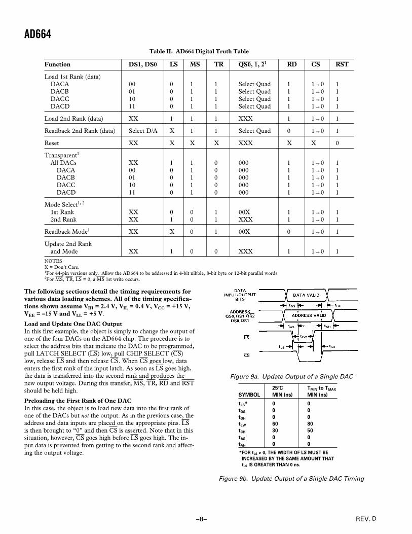
Figure 9a. Update Output of a Single DAC
258C TMIN to TMAX
SYMBOL MIN (ns) MIN (ns)
tLS* 0 0
tDS 0 0
tDH 0 0
tLW 60 80
tCH 30 50
tAS 0 0
tAH 0 0
*FOR tLS > 0, THE WIDTH OF LS MUST BE
INCREASED BY THE SAME AMOUNT THAT
tLS IS GREATER THAN 0 ns.
Figure 9b. Update Output of a Single DAC Timing
The following sections detail the timing requirements forvarious data loading schemes. All of the timing specifica-tions shown assume VIH = 2.4 V, VIL = 0.4 V, VCC = +15 V,VEE = –15 V and VLL = +5 V.
Load and Update One DAC OutputIn this first example, the object is simply to change the output ofone of the four DACs on the AD664 chip. The procedure is toselect the address bits that indicate the DAC to be programmed,pull LATCH SELECT (LS) low, pull CHIP SELECT (CS)low, release LS and then release CS. When CS goes low, dataenters the first rank of the input latch. As soon as LS goes high,the data is transferred into the second rank and produces thenew output voltage. During this transfer, MS, TR, RD and RSTshould be held high.
Preloading the First Rank of One DACIn this case, the object is to load new data into the first rank ofone of the DACs but not the output. As in the previous case, theaddress and data inputs are placed on the appropriate pins. LSis then brought to “0” and then CS is asserted. Note that in thissituation, however, CS goes high before LS goes high. The in-put data is prevented from getting to the second rank and affect-ing the output voltage.
D
AD664
REV. –9–
Figure 10a. Preload First Rank of a DAC
258C TMIN to TMAX
SYMBOL MIN (ns) MIN (ns)
tLS 0 0
tLH 15 15
tCW 80 100
tDS 0 0
tDH 15 15
tAS 0 0
tAH 15 15
Figure 10b. Preload First Rank of a DAC Timing
This allows the user to “preload” the data to a DAC and strobeit into the output latch at some future time. The user could dothis by reproducing the sequence of signals illustrated in thenext section.
Update Second Rank of a DACAssuming that a new input code had previously been placed intothe first rank of the input latches, the user can update the out-put of the DAC by simply pulling CS low while keeping LS,MS, TR, RD and RST high. Address data is not needed in thiscase. In reality, all second ranks are being updated by this pro-cedure, but only those which receive data different from thatalready there would manifest a change. Updating the secondrank does not change the contents of the first rank.
Figure 11. Update Second Rank of a DAC
The same options that exist for individual DAC input loadingalso exist for multiple DAC input loading. That is, the user canchoose to update the first and second ranks of the registers orpreload the first ranks and then update them at a future time.
Preload Multiple First Rank RegistersThe first ranks of the DAC input registers may be preloadedwith new input data without disturbing the second rank data.This is done by transferring the data into the first rank by bring-ing CS low while LS is low. But CS must return high before LS.This prevents the data from the first rank from getting into thesecond rank. A simple second rank update cycle as shown inFigure 11 would move the “preloaded” information to theDACs.
Figure 12. Preload First Rank Registers
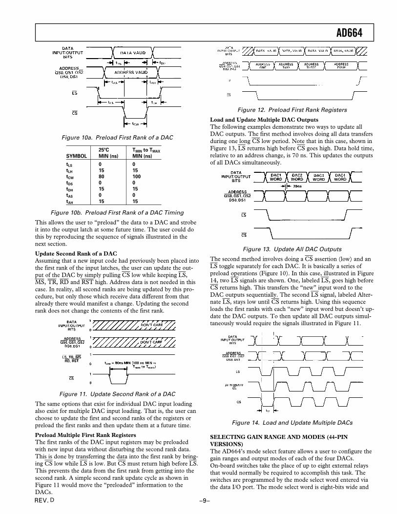
Load and Update Multiple DAC OutputsThe following examples demonstrate two ways to update allDAC outputs. The first method involves doing all data transfersduring one long CS low period. Note that in this case, shown inFigure 13, LS returns high before CS goes high. Data hold time,relative to an address change, is 70 ns. This updates the outputsof all DACs simultaneously.
Figure 13. Update All DAC Outputs
The second method involves doing a CS assertion (low) and anLS toggle separately for each DAC. It is basically a series ofpreload operations (Figure 10). In this case, illustrated in Figure14, two LS signals are shown. One, labeled LS, goes high beforeCS returns high. This transfers the “new” input word to theDAC outputs sequentially. The second LS signal, labeled Alter-nate LS, stays low until CS returns high. Using this sequenceloads the first ranks with each “new” input word but doesn’t up-date the DAC outputs. To then update all DAC outputs simul-taneously would require the signals illustrated in Figure 11.
Figure 14. Load and Update Multiple DACs
SELECTING GAIN RANGE AND MODES (44-PINVERSIONS)The AD664’s mode select feature allows a user to configure thegain ranges and output modes of each of the four DACs.On-board switches take the place of up to eight external relaysthat would normally be required to accomplish this task. Theswitches are programmed by the mode select word entered viathe data I/O port. The mode select word is eight-bits wide and
D
AD664
REV. –10–
occupies the topmost eight bits of the input word. The last fourbits of the input word are “don’t cares.”
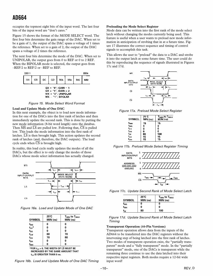
Figure 15 shows the format of the MODE SELECT word. Thefirst four bits determine the gain range of the DAC. When set tobe a gain of 1, the output of the DAC spans a voltage of 1 timesthe reference. When set to a gain of 2, the output of the DACspans a voltage of 2 times the reference.
The next four bits determine the mode of the DAC. When set toUNIPOLAR, the output goes from 0 to REF or 0 to 2 REF.When the BIPOLAR mode is selected, the output goes from–REF/2 to REF/2 or –REF to REF.
Figure 15. Mode Select Word Format
Load and Update Mode of One DACIn this next example, the object is to load new mode informa-tion for one of the DACs into the first rank of latches and thenimmediately update the second rank. This is done by putting thenew mode information (8-bit word length) onto the databus.Then MS and LS are pulled low. Following that, CS is pulledlow. This loads the mode information into the first rank oflatches. LS is then brought high. This action updates the secondrank of latches (and, therefore, the DAC outputs). The loadcycle ends when CS is brought high.
In reality, this load cycle really updates the modes of all theDACs, but the effect is to only change the modes of thoseDACs whose mode select information has actually changed.
Figure 16a. Load and Update Mode of One DAC
258C TMIN to TMAX
SYMBOL MIN (ns) MIN (ns)
tMS 0 0
tLS* 0 0
tDS 0 0
tLW 60 70
tCH 70 80
tDH 0 0
tMH 0 0
*FOR tLS > 0, THE WIDTH OF LS MUST BE
INCREASED BY THE SAME AMOUNT THAT
tLS IS GREATER THAN 0 ns.
Figure 16b. Load and Update Mode of One DAC Timing
Preloading the Mode Select RegisterMode data can be written into the first rank of the mode selectlatch without changing the modes currently being used. Thisfeature is useful when a user wants to preload new mode infor-mation in anticipation of strobing that in at a future time. Fig-ure 17 illustrates the correct sequence and timing of controlsignals to accomplish this task.
This allows the user to “preload” the data to a DAC and strobeit into the output latch at some future time. The user could dothis by reproducing the sequence of signals illustrated in Figures17c and 17d.
Figure 17a. Preload Mode Select Register
Figure 17b. Preload Mode Select Register Timing
1
0
1
0
DATA INPUT/OUTPUT
BITS
ADDRESSQS0,QS1,QS2
DS0,DS1
_________
__MS
__CS
tMS tMH
tW
Figure 17c. Update Second Rank of Mode Select Latch
258C TMIN to TMAX
SYMBOL MIN (ns) MIN (ns)
tMS 0 0
tMH 0 0
tW 80 100
Figure 17d. Update Second Rank of Mode Select Latch
Timing
Transparent Operation (44-Pin Versions)Transparent operation allows data from the inputs of theAD664 to be transferred into the DAC registers without theintervening step of being latched into the first rank of latches.Two modes of transparent operation exist, the “partially trans-parent” mode and a “fully transparent” mode. In the “partiallytransparent” mode, one of the DACs is transparent while theremaining three continue to use the data latched into theirrespective input registers. Both modes require a 12-bit wideinput word!
D
AD664
REV. –11–
OUTPUT DATATwo types of outputs may be obtained from the internal dataregisters of the AD664 chip, mode select and DAC input codedata. Readback data may be in the same forms in which it canbe entered; 4-, 8-, and 12-bit wide words (12 bits only for28-pin versions).
DAC Data ReadbackDAC input code readback data is obtained by setting the addressof the DAC (DS0, DS1) and Quads (QS0, QS1, QS2) on theaddress pins and bringing the RD and CS pins low. The timingdiagram for a DAC code readback operation appears in Figure 20.
Figure 20a. DAC Input Code Readback
25°C TMIN to TMAX
SYMBOL MIN (ns) MIN (ns)
tAS 0 0
tRS 0 0
tDV 150 180
tDF 60 75
tAH 0 0
tRH 0 0
Figure 20b. DAC Input Code Readback Timing
Mode Data ReadbackMode data is read back in a similar fashion. By setting MS, QS0,QS1, RD and CS low while setting TR and RST high, the modeselect word is presented to the I/O port pins. Figure 21 shows thetiming diagram for a readback of the mode select data register.
Figure 21a. Mode Data Readback
258C TMIN to TMAX
SYMBOL MIN (ns) MIN (ns)
tAS 0 0
tMS 0 0
tDV 150 180
tDF 60 75
tAH 0 0
tMH 0 0
Figure 21b. DAC Mode Readback Timing
Fully transparent operation can be thought of as a simultaneousload of data from Figure 9a where replacing LS with TR causesall 4 DACs to be loaded at once.
The Fully transparent mode is achieved by asserting lows onQS0, QS1, QS2, TR and CS while keeping LS high in additionto MS and RB. Figure 18a illustrates the necessary timing rela-tionships. Fully transparent operation will also work with TRtied low (enabled).
DATA INPUT/OUTPUT BITS
tTS
tDS
tQH
tDH
tQS
DATA VALID
TWt
tCH
1LS
QS
TR
CS
Figure 18a. Fully Transparent Mode
258C TMIN to TMAX
SYMBOL MIN (ns) MIN (ns)
tAS 0 0
tQS 0 0
tTS* 0 0
tTW 80 90
tCH 90 110
tDH 0 0
tQH 0 0
*FOR tTS > 0, THE WIDTH OF TR MUST BE
INCREASED BY THE SAME AMOUNT THAT
tTS IS GREATER THAN 0 ns.
Figure 18b. Fully Transparent Mode Timing
Partially transparent operation can be thought of as preloadingthe first rank in Figure 10a without requiring the additional CSpulse from Figure 11.
The partially transparent mode is achieved by setting CS, QS0,QS1, QS2, LS, and TR low while keeping RD and MS high.The address of the transparent DAC is asserted on DS0 andDS1. Figure 19a illustrates the necessary timing relationships.Partially transparent operation will also work with TR tied low(enabled).
DATA INPUT/OUTPUT BITS
ADDRESSQS0, QS1, QS2
DS0, DS1, LS
tTS
tAS
tDH
DATA VALID
Wt tTH
TR
CS
ADDRESS VALID
tAH
tDS
Figure 19a. Partially Transparent
25°C TMIN to TMAX
SYMBOL MIN (ns) MIN (ns)
tDS 0 0
tAS 0 0
tTS 0 0
tW 90 110
tDH 15 15
tAH 15 15
tTH 15 15
Figure 19b. Partially Transparent Mode Timing
D
AD664
REV. –12–
Output LoadsReadback timing is tested with the output loads shown in Figure22.
Figure 22. Output Loads
Asynchronous Reset OperationThe asynchronous reset signal shown in Figure 23 may beasserted at any time. A minimum pulse width (tRW) of 90 ns isrequired. The reset feature is designed to return all DAC out-puts to 0 volts regardless of the mode or range selected. In the44-pin versions, the modes are reset to unipolar 10 V span (gainof 1), and the input codes are rewritten to be “0s.” PreviousDAC code and mode information is erased.
Figure 23a. Asynchronous Reset Operation
Figure 23b. Asynchronous Reset Operation Timing
In the 28-pin versions of the AD664, the mode remainsunchanged, the appropriate input code is rewritten to reset theoutput voltage to 0 volts. As in the 44-pin versions, the previousinput data is erased.
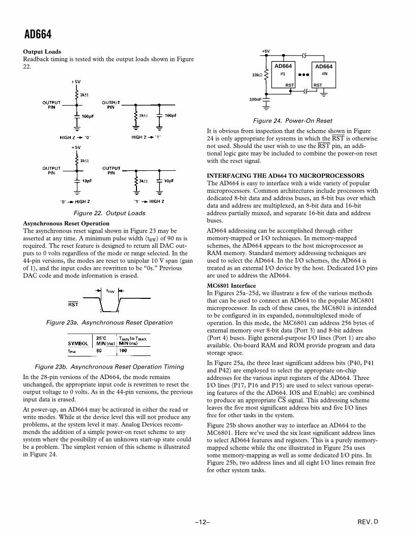
At power-up, an AD664 may be activated in either the read orwrite modes. While at the device level this will not produce anyproblems, at the system level it may. Analog Devices recom-mends the addition of a simple power-on reset scheme to anysystem where the possibility of an unknown start-up state couldbe a problem. The simplest version of this scheme is illustratedin Figure 24.
AD664 AD664
+5V
10kΩ
100nF
#1
RST
#N
RST
Figure 24. Power-On Reset
It is obvious from inspection that the scheme shown in Figure24 is only appropriate for systems in which the RST is otherwisenot used. Should the user wish to use the RST pin, an addi-tional logic gate may be included to combine the power-on resetwith the reset signal.
INTERFACING THE AD664 TO MICROPROCESSORSThe AD664 is easy to interface with a wide variety of popularmicroprocessors. Common architectures include processors withdedicated 8-bit data and address buses, an 8-bit bus over whichdata and address are multiplexed, an 8-bit data and 16-bitaddress partially muxed, and separate 16-bit data and addressbuses.
AD664 addressing can be accomplished through eithermemory-mapped or I/O techniques. In memory-mappedschemes, the AD664 appears to the host microprocessor asRAM memory. Standard memory addressing techniques areused to select the AD664. In the I/O schemes, the AD664 istreated as an external I/O device by the host. Dedicated I/O pinsare used to address the AD664.
MC6801 InterfaceIn Figures 25a–25d, we illustrate a few of the various methodsthat can be used to connect an AD664 to the popular MC6801microprocessor. In each of these cases, the MC6801 is intendedto be configured in its expanded, nonmultiplexed mode ofoperation. In this mode, the MC6801 can address 256 bytes ofexternal memory over 8-bit data (Port 3) and 8-bit address(Port 4) buses. Eight general-purpose I/O lines (Port 1) are alsoavailable. On-board RAM and ROM provide program and datastorage space.
In Figure 25a, the three least significant address bits (P40, P41and P42) are employed to select the appropriate on-chipaddresses for the various input registers of the AD664. ThreeI/O lines (P17, P16 and P15) are used to select various operat-ing features of the the AD664. IOS and E(nable) are combinedto produce an appropriate CS signal. This addressing schemeleaves the five most significant address bits and five I/O linesfree for other tasks in the system.
Figure 25b shows another way to interface an AD664 to theMC6801. Here we’ve used the six least significant address linesto select AD664 features and registers. This is a purely memory-mapped scheme while the one illustrated in Figure 25a usessome memory-mapping as well as some dedicated I/O pins. InFigure 25b, two address lines and all eight I/O lines remain freefor other system tasks.
D
AD664
REV. –13–
Figure 25a. Simple AD664 to MC6801 Interface
Expansion of the scheme employed in Figure 25a results in thatshown in Figure 25c. Here, two AD664s are connected to anMC6801, providing a total of eight 12-bit, software program-mable DACs. Again, the three least significant bits of addressare used to select the on-chip registers of the AD664. IOS andE, as well as a fourth address bit, are decoded to provide theappropriate CS signals. Four address and five I/O lines remainuncommitted.
A slightly more sophisticated approach to system expansion isillustrated in Figure 25d. Here, a 74LS138 (1-of-8 decoder) isused to address one of the eight AD664s connected to theMC6801. The three least significant address bits are used toselect on-chip register and DAC. The next three address bits areused to select the appropriate AD664. IOS and E gate the74LS138 output.
Figure 25b. Alternate AD664 to MC6801 Interface
Figure 25c. Interfacing Two AD664s to an MC6801
D
AD664
REV. –14–
The schemes in Figure 25 illustrate some of the trade-offs whicha designer may make when configuring a system. For example,the designer may use I/O lines instead of address bits or viceversa. This decision may be influenced by other I/O tasks or sys-tem expansion requirements. He/she can also choose to imple-ment only a subset of the features available. Perhaps the RSTpin isn’t really needed. Tying that input pin to VLOGIC frees upanother I/O or address bit. The same consideration applies tomode select. In all of these cases TR is shown tied to VLOGIC,because the MC6801 cannot provide the 12-bit-wide inputword required for the transparent mode. In situations wheretransparent operation isn’t required, and mode select is also notneeded, the designer may consider specifying the DIP version ofthe device (either the UNI or BIP version).
Each of the schemes illustrated in Figure 25 operates with anMC6801 at clock rates up to and including 1.5 MHz. Similarschemes can be derived for other 8-bit microprocessors andmicrocontrollers such as the 8051/8086/8088/6502, etc. Onesuch scheme developed for the 8051/AD664 is illustrated inFigure 26.
8051 InterfaceFigure 26 shows the AD664 combined with an 8051 µcontrollerchip. Three LSBs of address provide the quad and DAC selectsignals. Control signals from Port 1 select various operatingmodes such as readback, mode select and reset as well as pro-viding the LS signal. Read and write signals from the 8051 aredecoded to provide the CS signal.
Figure 25d. Interfacing Eight AD664s to an MC6801
D
AD664
REV. –15–
IBM PC* InterfaceFigure 27 illustrates a simple interface between an IBM PC andan AD664. The three least significant address bits are used toselect the Quad and DAC. The next two address bits are usedfor LS and MS. In this scheme, a 12-bit input word requirestwo load cycles, an 8-bit word and a 4-bit word. Another write
is required to transfer the word or words previously written tothe second rank. A 12-bit-wide word again requires at least tworead cycles; one for the 8 MSBs and four for the LSBs. Thepage select signal produces a CS strobe for any address from300H to 31FH.
Figure 26. AD664 to 8051 Interface
Figure 27. AD664 to IBM PC Interface
*IBM PC is a trademark of International Business Machines Corp.
D
AD664
REV. –16–
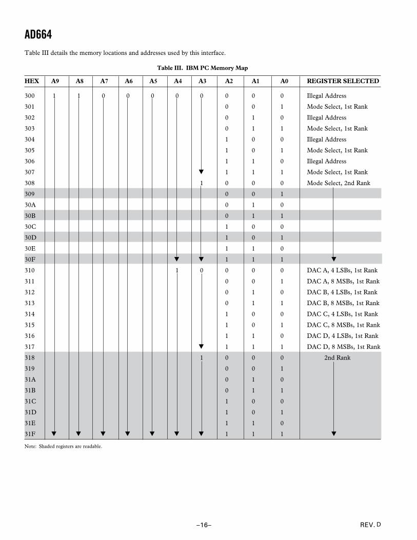
Table III details the memory locations and addresses used by this interface.
The following IBM PC Basic routine produces four output volt-age ramps from one AD664. Line numbers 10 through 70 de-fine the hardware addresses for the first and second ranks ofDAC registers as well as the first and second ranks of the modeselect register. Program variables are initialized in line numbers110 through 130. Line number 170 writes “0s” out to the firstrank and, then, the second rank of the mode select register.
Line numbers 200 through 320 calculate output voltages. Fi-nally line numbers 410 through 450 update the first, then thesecond ranks of the DAC input registers. Hardware registersmay be read with the “INP” instruction. For example, the con-tents of the DAC A register may be accessed with the followingcom mand: Line# A = INP(DACA).
5 REM----AD664 LISSAJOUS PATTERNS----10 REM ---ASSIGN HARDWARE ADDRESSES---20 DACA = 78530 DACB = 78740 DACC = 78950 DACD = 79160 DAC2ND = 79270 MODE1 = 769: MODE2 = 77680 REM90 REM100 REM ---INITIALIZE VARIABLES---110 X = 0: Y1 = 128: Y2 = 64: Y3 = 32120 CX = 1: CY1 = 1: CY2 = -1: CY3= 1130 FX = 9: FY1 = 5: FY2 = 13: FY3 = 15140 REM150 REM160 REM ---INITIALIZE MODES AND GAINS--- 170 OUT MODE1,0: OUT MODE2,0180 REM190 REM200 REM ---CALCULATE VARIABLES---210 X = X + FX*CX220 Y1 = Y1 + FY1*CY1230 Y2 = Y2 + FY2*CY2240 Y3 = Y3 + FY3*CY3250 IF X > 255 THEN X = 255: CX = -1: GOTO 270260 IF X < 0 THEN X = 0: CX = 1270 IF Y1 > 255 THEN Y1 = 255: CY1 = -1: GOTO 290280 IF Y1 < 0 THEN Y1 = 0: CY1 = 1290 IF Y2 > 255 THEN Y2 = 255: CY2 = -1 GOTO 310300 IF Y2 < 0 THEN Y2 = 0: CY2 = -1310 IF Y3 > 255 THEN Y3 = 255: CY3 = -1: GOTO 400320 IF Y3 < 0 THEN Y3 = 0: CY3 = 1330 REM340 REM400 REM ---SEND DAC DATA---410 OUT DACA,X420 OUT DACB,Yl430 OUT DACC,Y2440 OUT DACD,Y3450 OUT DAC2ND,0500 REM510 REM520 REM ---LOOP BACK--- 530 GOTO 210
D
AD664
REV. –18–
Simple AD664 to MC68000 InterfaceFigure 28 shows an AD664 connected to an MC68000. In thismemory-mapped I/O scheme, the “left-justified” data is writtenin one 12-bit input word. Four address bits are used to performthe on-chip D/A selection as well as the various operating fea-tures. The R/W signal controls the RD function and systemreset controls RST.
This scheme can be converted to write “right-justified’’ data byconnecting the data inputs to DATA bits D0 through D11respectively. Other options include controlling the QS0, QS1and QS2 pins with UDS and LDS to provide a way to write8-bit input and read 8-bit output words.
Figure 28. AD664 to MC68000 Interface
D
AD664
REV. –19–
Figure 29. AD664 in “Tester-per-Pin” Architecture
APPLICATIONS OF THE AD664“Tester-Per-Pin” ATE ArchitectureFigure 29 shows the AD664 used in a single channel of a digitaltest system. In this scheme, the AD664 supplies four individualoutput voltages. Two are provided to the VHIGH and VLOW in-puts of the AD345 pin driver I.C. to set the digital output levels.Two others are routed to the inputs of the AD96687 dual com-parator to supply reference levels of the readback features. Thisapproach can be replicated to give as many channels of stimulus/readback as the tester has pins. The AD664 is a particularlyappropriate choice for a large-scale system because the lowpower requirements (under 500 mW) ease power supply andcooling requirements. Analog ground currents of 600 µA or lessmake the ground current management task simpler. All DACscan be driven from the same system reference and will trackover time and temperature. Finally, the small board arearequired by the AD664 (and AD345 and AD96687) allows ahigh functional density.
X-Y PlottersFigure 30 is a block diagram of the control section of amicroprocessor-controlled X-Y pen plotter. In this conceptualexercise, two of the DACs are used for the X-channel drive andtwo are used for the Y-channel drive. Each provides either thecoarse or fine movement control for its respective channel. Thisapproach offers increased resolution over some other approaches.
A designer can take advantage of the reset feature of the AD664in the following manner. If the system is designed such that the“HOME” position of the pen (or galvanometer, beam, head orsimilar mechanism) results when the outputs of all of the DACsare at zero, then no system software is required to home thepen. A simple reset signal is sufficient.
Similarly, the transparent feature could be used to the sameend. One code can be sent to all DACs at the same time to sendthe pen to the home position. Of course, this would require
some software where the previous example would require only asingle reset strobe signal!
Drawing scaling can be achieved by taking advantage of theAD664’s software programmable gain settings. If, for example,an “A” size drawing is created with gain settings of 1, then a“C” size drawing can be created by simply resetting all DACgains to 2 and redrawing the object. Conversely, a “C” sizedrawing created with gains of 2 can be reduced to “A” size sim-ply by changing the gains to 1 and redrawing. The same princi-pal applies for conversion from “B” size to “D” size or “D” sizeto “B” size. The multiplying capability of the AD664 providesanother scaling option. Changing the reference voltage providesa proportional change in drawing size. Inverting the referencevoltage would invert the drawing.
Swapping digital input data from the X channel to the Y chan-nel would rotate the drawing 90 degrees.
CONTROLLING DIMENSIONS ARE IN INCHES; MILLIMETER DIMENSIONS(IN PARENTHESES) ARE ROUNDED-OFF INCH EQUIVALENTS FORREFERENCE ONLY AND ARE NOT APPROPRIATE FOR USE IN DESIGN.
CONTROLLING DIMENSIONS ARE IN INCHES; MILLIMETER DIMENSIONS(IN PARENTHESES) ARE ROUNDED-OFF INCH EQUIVALENTS FORREFERENCE ONLY AND ARE NOT APPROPRIATE FOR USE IN DESIGN.CORNER LEADS MAY BE CONFIGURED AS WHOLE LEADS.
(J-44) Dimensions shown in inches and (millimeters)
CONTROLLING DIMENSIONS ARE IN INCHES; MILLIMETER DIMENSIONS(IN PARENTHESES) ARE ROUNDED-OFF INCH EQUIVALENTS FORREFERENCE ONLY AND ARE NOT APPROPRIATE FOR USE IN DESIGN.
144
6
7
18
17
39
40
BOTTOM VIEW
29
28
0.055 (1.40)0.045 (1.14)
0.662 (16.82)0.640 (16.27)
SQ0.028 (0.71)0.022 (0.56)
0.020 (0.51)REF 45°
0.040 (1.02)REF 45°3 PLACES
0.050(1.27)BSC
0.075 (1.91) REF0.100 (2.54)0.064 (1.63)
022
10
6-A
CONTROLLING DIMENSIONS ARE IN INCHES; MILLIMETERS DIMENSIONS(IN PARENTHESES) ARE ROUNDED-OFF INCH EQUIVALENTS FORREFERENCE ONLY AND ARE NOT APPROPRIATE FOR USE IN DESIGN.
(P-44) Dimensions shown in inches and (millimeters)
ORDERING GUIDE Model1 Temperature Range Package Description Package Option 5962-8871901MXA −55°C to +125°C 28-Lead Side-Brazed SBDIP D-28-2 5962-8871902MXA −55°C to +125°C 28-Lead Side-Brazed SBDIP D-28-2 5962-8871903MYA −55°C to +125°C 44-Lead LCC E-44-1 AD664AD-BIP −40°C to +85°C 28-Lead Side-Brazed SBDIP D-28-2 AD664AD-UNI −40°C to +85°C 28-Lead Side-Brazed SBDIP D-28-2 AD664AJ −40°C to +85°C 44-Lead JLCC J-44 AD664BD-BIP −40°C to +85°C 28-Lead Side-Brazed SBDIP D-28-2 AD664BD-UNI −40°C to +85°C 28-Lead Side-Brazed SBDIP D-28-2 AD664BE −40°C to +85°C 44-Lead LCC E-44-1 AD664BJ −40°C to +85°C 44-Lead JLCC J-44 AD664JN-BIP 0°C to +70°C 28-Lead PDIP N-28-2 AD664JN-UNI 0°C to +70°C 28-Lead PDIP N-28-2 AD664JNZ-BIP 0°C to +70°C 28-Lead PDIP N-28-2 AD664JNZ-UNI 0°C to +70°C 28-Lead PDIP N-28-2 AD664JP 0°C to +70°C 44-Lead PLCC P-44 AD664JPZ 0°C to +70°C 44-Lead PLCC P-44 AD664KN-BIP 0°C to +70°C 28-Lead PDIP N-28-2 AD664KNZ-BIP 0°C to +70°C 28-Lead PDIP N-28-2 AD664KNZ-UNI 0°C to +70°C 28-Lead PDIP N-28-2 AD664KP 0°C to +70°C 44-Lead PLCC P-44 AD664KPZ 0°C to +70°C 44-Lead PLCC P-44 AD664SD-BIP −55°C to +125°C 28-Lead Side-Brazed SBDIP D-28-2 AD664SD-BIP/883B −55°C to +125°C 28-Lead Side-Brazed SBDIP D-28-2 AD664SD-UNI −55°C to +125°C 28-Lead Side-Brazed SBDIP D-28-2 AD664SD-UNI/883B −55°C to +125°C 28-Lead Side-Brazed SBDIP D-28-2 AD664TD-BIP −55°C to +125°C 28-Lead Side-Brazed SBDIP D-28-2 AD664TD-BIP/883B −55°C to +125°C 28-Lead Side-Brazed SBDIP D-28-2 AD664TD-UNI/883B −55°C to +125°C 28-Lead Side-Brazed SBDIP D-28-2 AD664TE/883B −55°C to +125°C 44-Lead LCC E-44-1 AD664TJ/883B −55°C to +125°C 44-Lead JLCC J-44 1 Z = RoHS Compliant Part.
COMPLIANT TO JEDEC STANDARDS MO-047-ACCONTROLLING DIMENSIONS ARE IN INCHES; MILLIMETER DIMENSIONS(IN PARENTHESES) ARE ROUNDED-OFF INCH EQUIVALENTS FORREFERENCE ONLY AND ARE NOT APPROPRIATE FOR USE IN DESIGN.


![UK BS 7671 16 VDE 0100 EN-60601/60335/60950/61010 VDE …download.flukecal.com/pub/literature/Fluke... · 2 [1] 50 kΩ 60 kΩ 100 kΩ / 20 V 500,000 8 10 kΩ 10 GΩ 4.5 CE Low Voltage](https://static.documents.pub/doc/80x56/5e7807e35be0b42eba4126eb/uk-bs-7671-16-vde-0100-en-60601603356095061010-vde-2-1-50-k-60-k-100-k.jpg)


