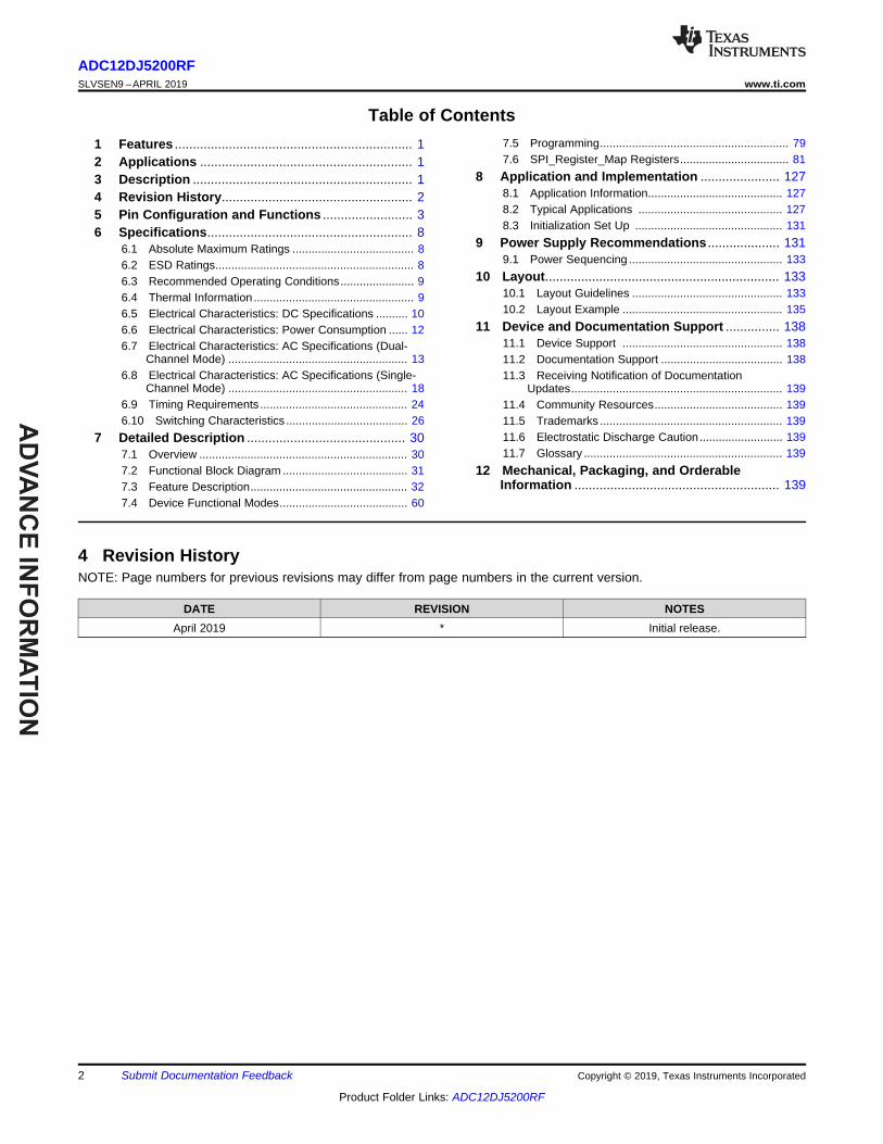
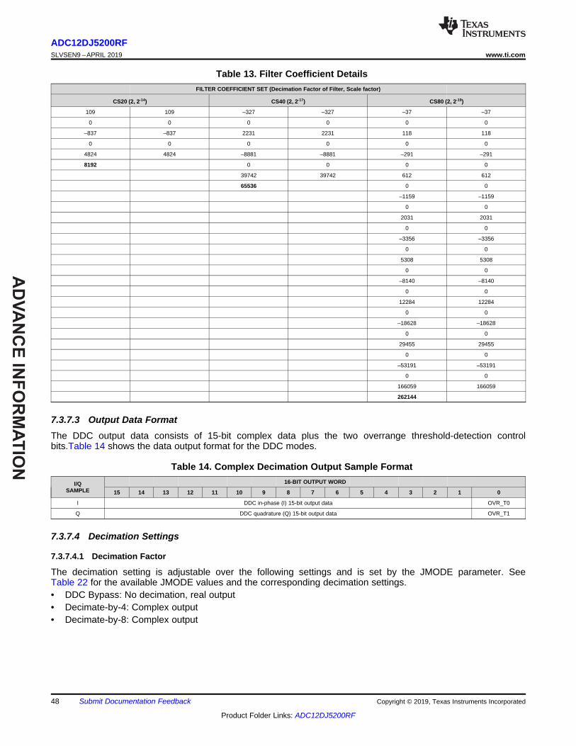
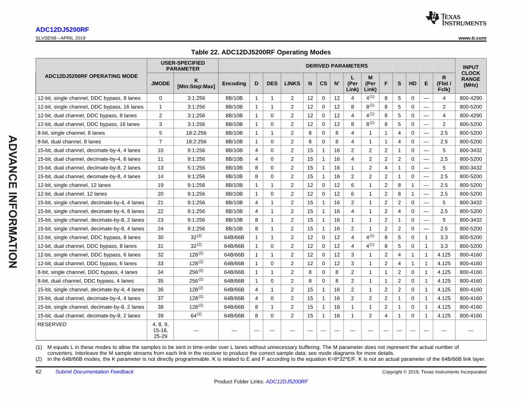
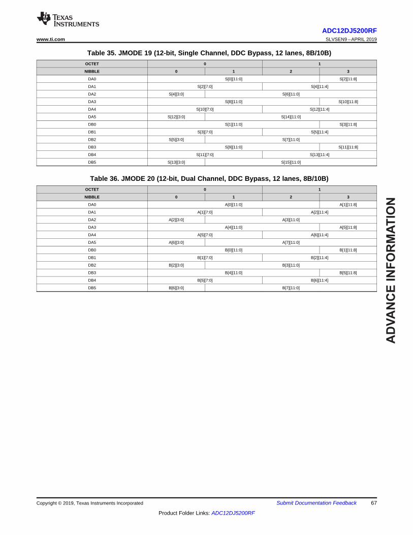
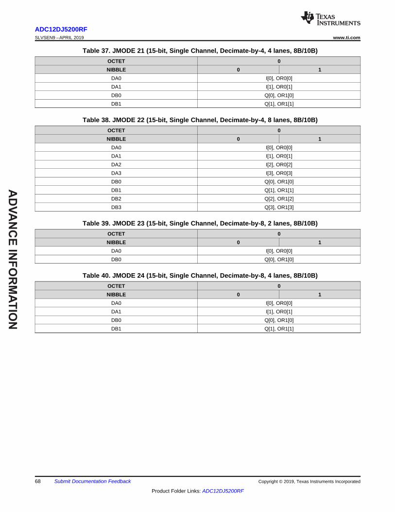
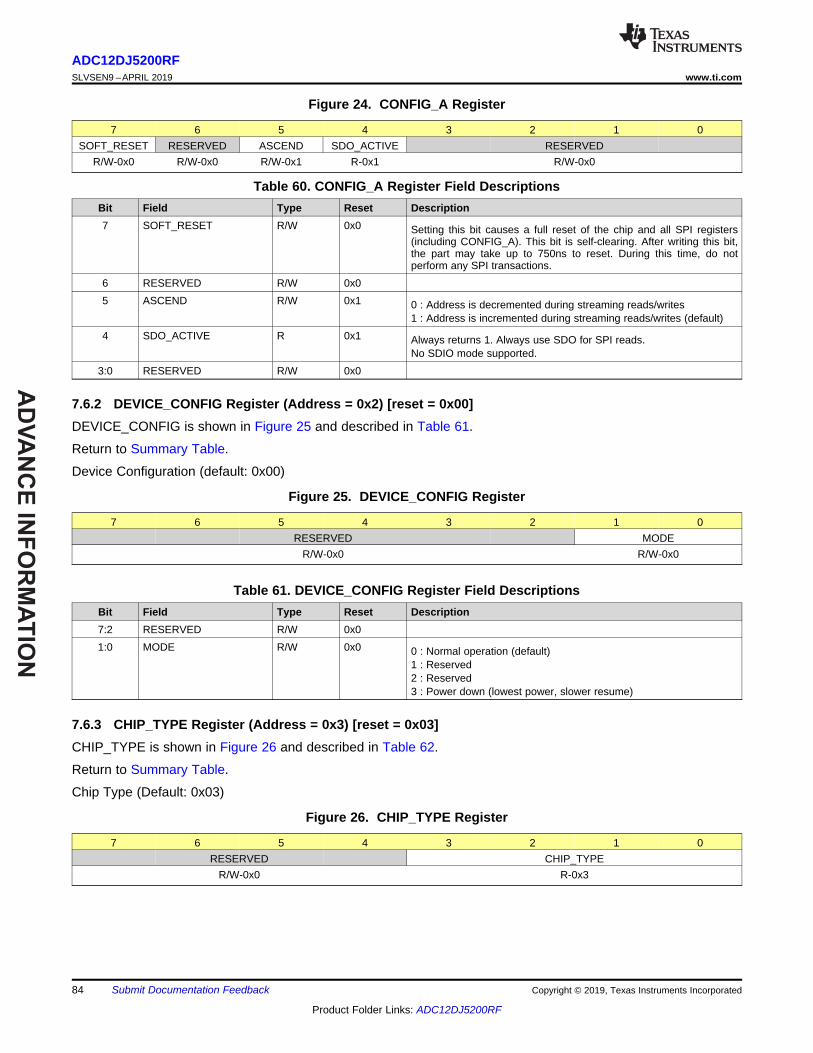
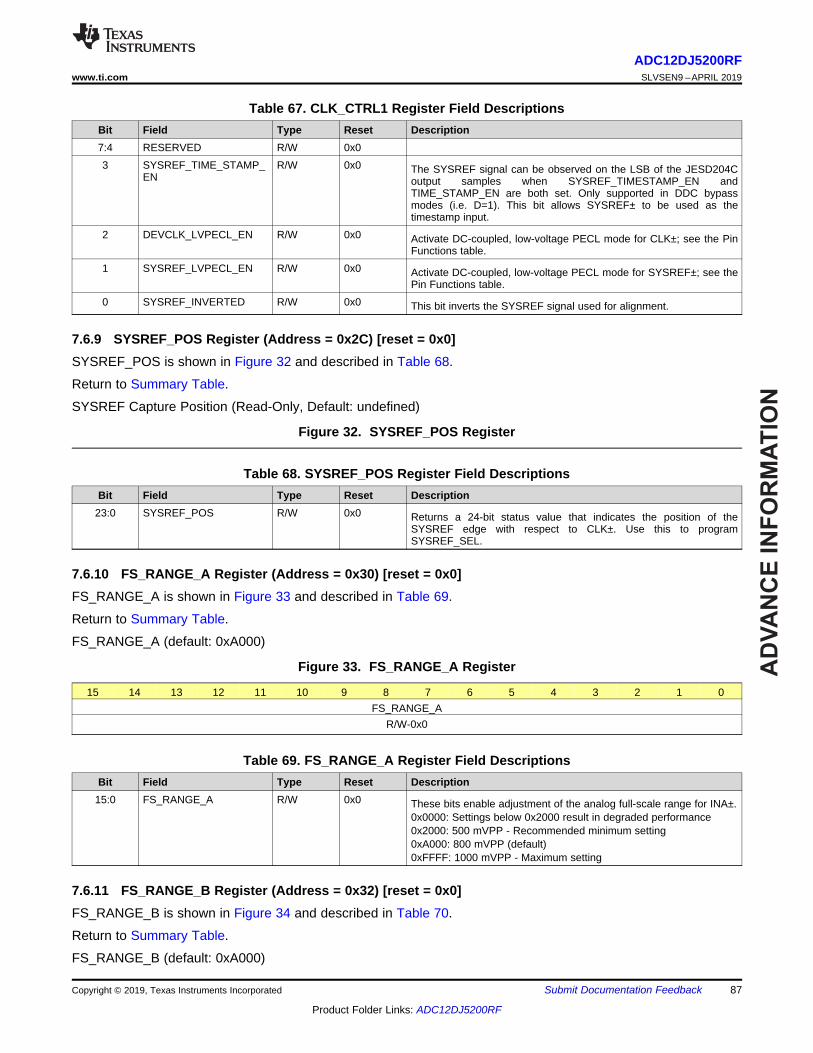
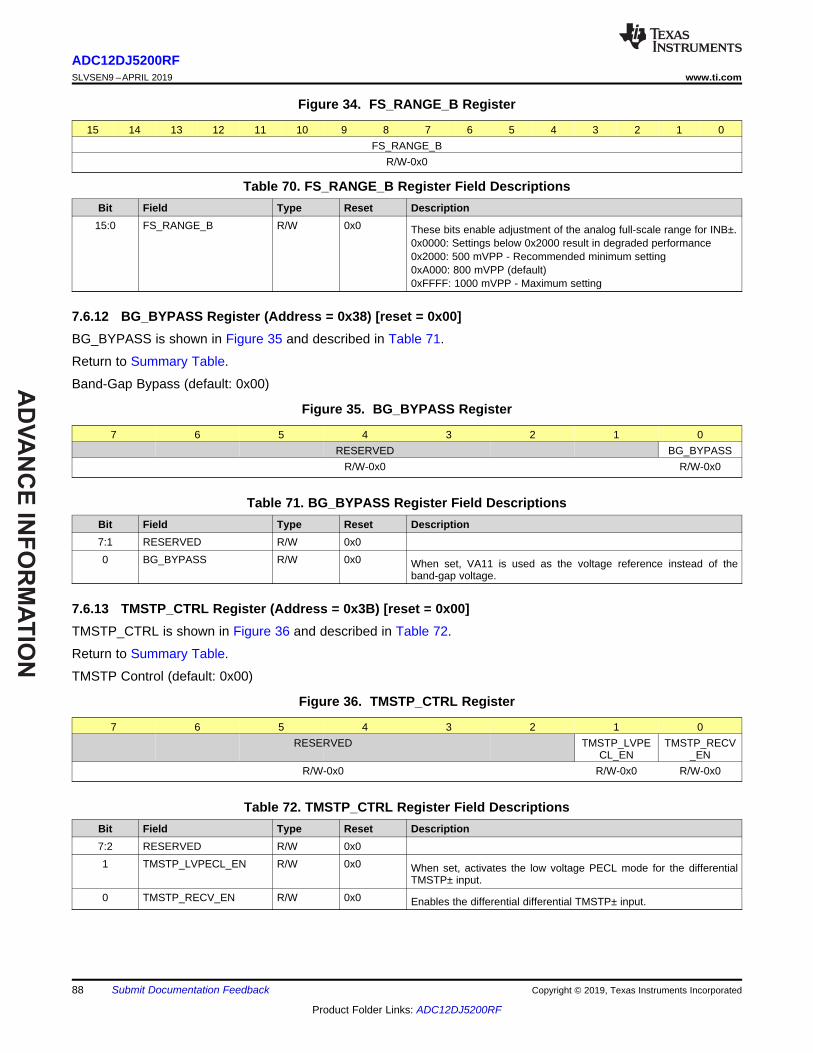
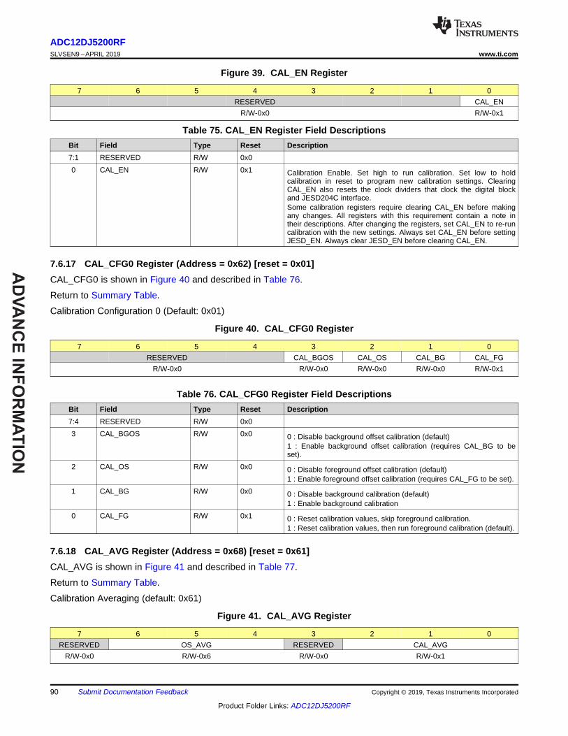
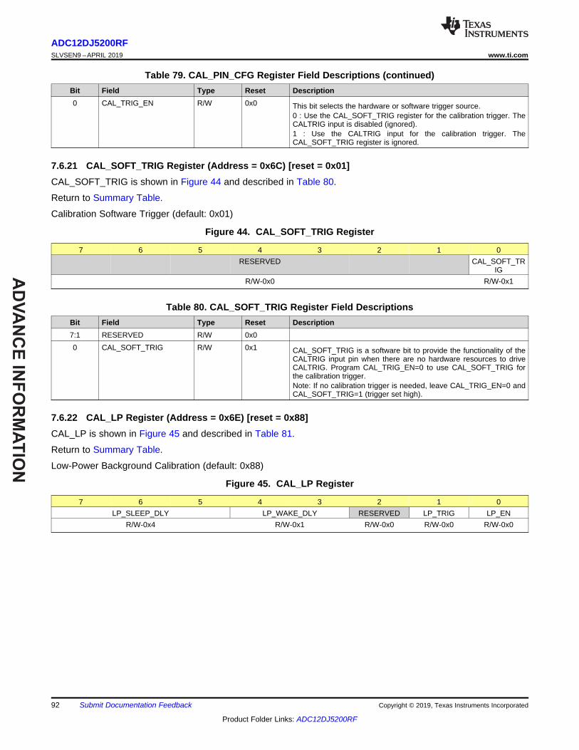
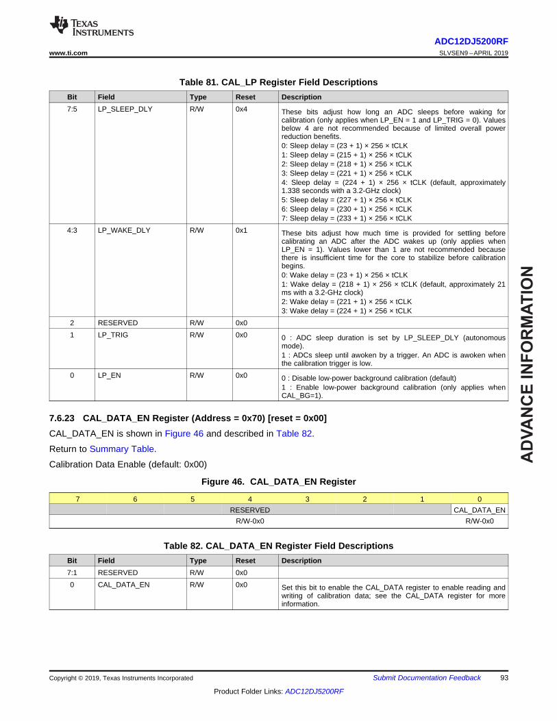
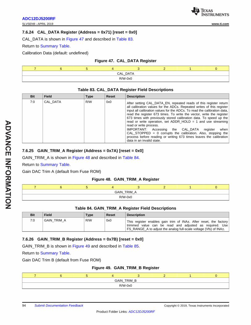
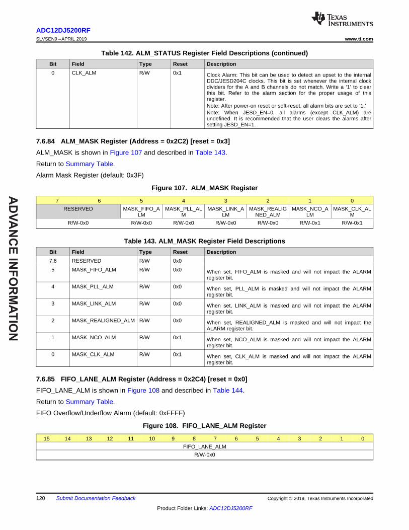
ADVANCE INFORMATION SCLK SDI SDO SCS\ NCOA0 NCOA1 NCOB0 NCOB1 ADC A JESD204C Link A JESD204C Link B Aperture Delay Adjust Clock Distribution and Synchronization CLK+ CLK- SYSREF+ SYSREF- SYNCSE\ Over- range DA0+ DA0- DA7+ DA7- DB0+ DB0- DB7+ DB7- Status Indicators ORA0 ORA1 ORB0 ORB1 CALSTAT ADC B TDIODE+ TDIODE- CALTRG PD SPI Registers and Device Control INA+ INA- INB+ INB- TMSTP+ TMSTP- Input MUX Input MUX JMODE SYSREF Windowing Crossbar MUX or Interleaving Digital Down Converter (DDC) Block DDC Options: DDC Bypass Decimate-by-4 Decimate-by-8 Product Folder Order Now Technical Documents Tools & Software Support & Community An IMPORTANT NOTICE at the end of this data sheet addresses availability, warranty, changes, use in safety-critical applications, intellectual property matters and other important disclaimers. ADVANCE INFORMATION for pre-production products; subject to change without notice. ADC12DJ5200RF SLVSEN9 – APRIL 2019 ADC12DJ5200RF 10.4-GSPS Single-Channel or 5.2-GSPS Dual-Channel, 12-bit, RF-Sampling Analog-to-Digital Converter (ADC) 1 1 Features 1• ADC core: – 12-bit resolution – Up to 10.4 GSPS in single-channel mode – Up to 5.2 GSPS in dual-channel mode • Performance specifications: – Noise floor (–20 dBFS, V FS = 1.0 V PP-DIFF ): – Dual-channel mode: –151.8 dBFS/Hz – Single-channel mode: –154.4 dBFS/Hz – ENOB (dual channel, F IN = 2.4 GHz): 8.6 Bits • Buffered analog inputs with V CMI of 0 V: – Analog input bandwidth (–3 dB): 8.0 GHz – Usable input frequency range: > 10 GHz – Full-scale input voltage (V FS , default): 0.8 V PP • Noiseless aperture delay (T AD ) adjustment: – Precise sampling control: 19-fs Step – Simplifies synchronization and interleaving – Temperature and voltage invariant delays • Easy-to-use synchronization features: – Automatic SYSREF timing calibration – Timestamp for sample marking • JESD204C serial data interface: – Maximum lane rate: 17.16 Gbps – Support for 64B/66B and 8B/10B encoding – 8B/10B modes are JESD204B compatible • Optional digital down-converters (DDC): – 4x and 8x complex decimation – Four independent 32-Bit NCOs per DDC • Power consumption: 4.0 W • Power supplies: 1.1 V, 1.9 V 2 Applications • Oscilloscopes and wideband digitizers • Communications testers (802.11ad, 5G) • Electronic warfare (SIGINT, ELINT) • Satellite communications (SATCOM) • RF-sampling software-defined radio (SDR) • Spectrometry 3 Description The ADC12DJ5200RF device is an RF-sampling, giga-sample, analog-to-digital converter (ADC) that can directly sample input frequencies from DC to above 10 GHz. ADC12DJ5200RF can be configured as a dual-channel, 5.2 GSPS ADC or single-channel, 10.4 GSPS ADC. These operating modes allow programmable tradeoffs in channel count and Nyquist bandwidth allows for flexible hardware that meets the needs of multiple applications. Useable input frequency range of up to 10 GHz enables direct RF sampling of L-band, S-band, C-band, and X-band for frequency agile systems. The ADC12DJ5200RF uses a high-speed JESD204C output interface with up to 16 serialized lanes supporting up to 17.16 Gbps line rate. Deterministic latency and multi-device synchronization is supported through JESD204C subclass-1. The JESD204C interface can be configured to trade-off line rate and number of lanes. Both 8B/10B and 64B/66B data encoding schemes are supported. 64b/66b encoding supports forward error correction (FEC) for improved bit error rates. The interface is backwards compatible with JESD204B receivers when using 8B/10B encoding modes. Innovative synchronization features, including noiseless aperture delay (T AD ) adjustment and SYSREF windowing, simplify system design for multi- channel applications. Optional digital down converters (DDCs) are available to provide digital conversion to baseband and to reduce the interface rate. Device Information (1) PART NUMBER PACKAGE BODY SIZE (NOM) ADC12DJ5200RF FCBGA (144) 10.00 mm × 10.00 mm (1) For all available packages, see the package option addendum at the end of the data sheet. ADC12DJ5200RF Block Diagram
Transcript
AD
VA
NC
E I
NF
OR
MA
TIO
NSCLK
SDI
SDO
SCS\
NCOA0 NCOA1 NCOB0 NCOB1
ADC AJESD204C
Link A
JESD204C
Link B
Aperture
Delay Adjust
Clock Distribution
and Synchronization
CLK+
CLK-
SYSREF+
SYSREF-
SYNCSE\Over-
range
DA0+
DA0-
DA7+
DA7-
DB0+
DB0-
DB7+
DB7-
Status
Indicators
ORA0
ORA1
ORB0
ORB1
CALSTAT
ADC B
TDIODE+ TDIODE-
CALTRG PD
SPI Registers and
Device Control
INA+
INA-
INB+
INB-
TMSTP+
TMSTP-
Input
MUX
Input
MUX
JMODE
SYSREF
Windowing
Crossbar MUX
or Interleaving
Digital Down
Converter (DDC)
Block
DDC Options:
DDC Bypass
Decimate-by-4
Decimate-by-8
Product
Folder
Order
Now
Technical
Documents
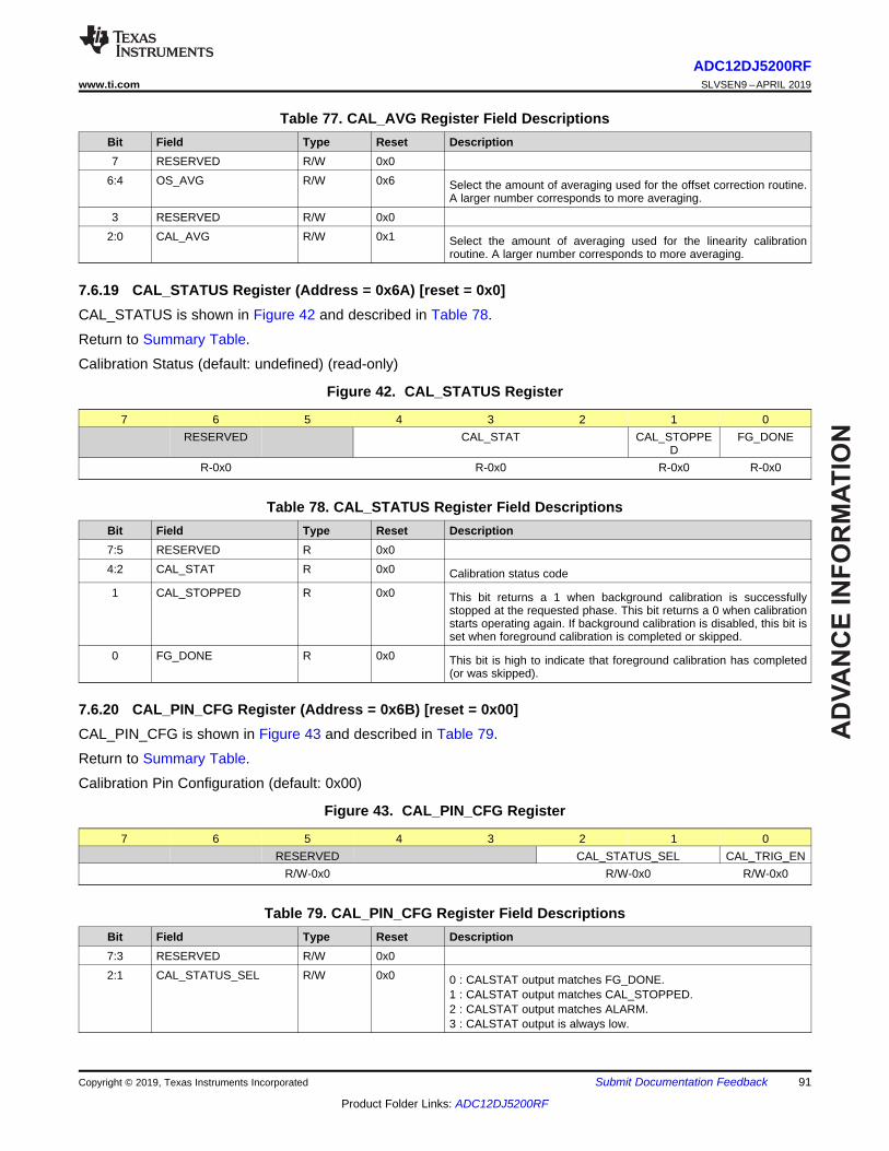
Tools &
Software
Support &Community
An IMPORTANT NOTICE at the end of this data sheet addresses availability, warranty, changes, use in safety-critical applications,intellectual property matters and other important disclaimers. ADVANCE INFORMATION for pre-production products; subject tochange without notice.
ADC12DJ5200RFSLVSEN9 –APRIL 2019
ADC12DJ5200RF 10.4-GSPS Single-Channel or 5.2-GSPS Dual-Channel,12-bit, RF-Sampling Analog-to-Digital Converter (ADC)
1
1 Features1• ADC core:
– 12-bit resolution– Up to 10.4 GSPS in single-channel mode– Up to 5.2 GSPS in dual-channel mode
– ENOB (dual channel, FIN = 2.4 GHz): 8.6 Bits• Buffered analog inputs with VCMI of 0 V:
– Analog input bandwidth (–3 dB): 8.0 GHz– Usable input frequency range: > 10 GHz– Full-scale input voltage (VFS, default): 0.8 VPP
• Noiseless aperture delay (TAD) adjustment:– Precise sampling control: 19-fs Step– Simplifies synchronization and interleaving– Temperature and voltage invariant delays
3 DescriptionThe ADC12DJ5200RF device is an RF-sampling,giga-sample, analog-to-digital converter (ADC) thatcan directly sample input frequencies from DC toabove 10 GHz. ADC12DJ5200RF can be configuredas a dual-channel, 5.2 GSPS ADC or single-channel,10.4 GSPS ADC. These operating modes allowprogrammable tradeoffs in channel count and Nyquistbandwidth allows for flexible hardware that meets theneeds of multiple applications. Useable inputfrequency range of up to 10 GHz enables direct RFsampling of L-band, S-band, C-band, and X-band forfrequency agile systems.
The ADC12DJ5200RF uses a high-speed JESD204Coutput interface with up to 16 serialized lanessupporting up to 17.16 Gbps line rate. Deterministiclatency and multi-device synchronization is supportedthrough JESD204C subclass-1. The JESD204Cinterface can be configured to trade-off line rate andnumber of lanes. Both 8B/10B and 64B/66B dataencoding schemes are supported. 64b/66b encodingsupports forward error correction (FEC) for improvedbit error rates. The interface is backwards compatiblewith JESD204B receivers when using 8B/10Bencoding modes.
Innovative synchronization features, includingnoiseless aperture delay (TAD) adjustment andSYSREF windowing, simplify system design for multi-channel applications. Optional digital down converters(DDCs) are available to provide digital conversion tobaseband and to reduce the interface rate.
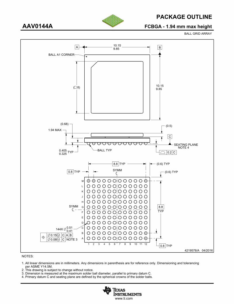
Device Information(1)
PART NUMBER PACKAGE BODY SIZE (NOM)ADC12DJ5200RF FCBGA (144) 10.00 mm × 10.00 mm
(1) For all available packages, see the package option addendumat the end of the data sheet.
11 Device and Documentation Support ............... 13811.1 Device Support .................................................. 13811.2 Documentation Support ...................................... 13811.3 Receiving Notification of Documentation
— Analog supply ground. Tie AGND and DGND to a common ground plane (GND) on the circuitboard.
BG C3 OBand-gap voltage output. This pin is capable of sourcing only small currents and driving limitedcapacitive loads, as specified in the Recommended Operating Conditions table. This pin can beleft disconnected if not used.
CALSTAT F7 O Foreground calibration status output or device alarm output. Functionality is programmed throughCAL_STATUS_SEL. This pin can be left disconnected if not used.
CALTRIG E7 IForeground calibration trigger input. This pin is only used if hardware calibration triggering isselected in CAL_TRIG_EN, otherwise software triggering is performed using CAL_SOFT_TRIG.Tie this pin to GND if not used.
CLK+ F1 I
Device (sampling) clock positive input. The clock signal is strongly recommended to be AC-coupled to this input for best performance. In single-channel mode, the analog input signal issampled on both the rising and falling edges. In dual-channel mode, the analog signal is sampledon the rising edge. This differential input has an internal untrimmed 100-Ω differential terminationand is self-biased to the optimal input common-mode voltage as long as DEVCLK_LVPECL_ENis set to 0.
CLK– G1 I Device (sampling) clock negative input. TI strongly recommends using AC-coupling for bestperformance.
DA0+ E12 OHigh-speed serialized data output for channel A, lane 0, positive connection. This differentialoutput must be AC-coupled and must always be terminated with a 100-Ω differential terminationat the receiver. This pin can be left disconnected if not used.
DA0– F12 O High-speed serialized data output for channel A, lane 0, negative connection. This pin can be leftdisconnected if not used.
DA1+ C12 OHigh-speed serialized data output for channel A, lane 1, positive connection. This differentialoutput must be AC-coupled and must always be terminated with a 100-Ω differential terminationat the receiver. This pin can be left disconnected if not used.
DA1– D12 O High-speed serialized data output for channel A, lane 1, negative connection. This pin can be leftdisconnected if not used.
DA2+ A10 OHigh-speed serialized-data output for channel A, lane 2, positive connection. This differentialoutput must be AC-coupled and must always be terminated with a 100-Ω differential terminationat the receiver. This pin can be left disconnected if not used.
DA2– A11 O High-speed serialized-data output for channel A, lane 2, negative connection. This pin can be leftdisconnected if not used.
DA3+ A8 OHigh-speed serialized-data output for channel A, lane 3, positive connection. This differentialoutput must be AC-coupled and must always be terminated with a 100-Ω differential terminationat the receiver. This pin can be left disconnected if not used.
DA3– A9 O High-speed serialized-data output for channel A, lane 3, negative connection. This pin can be leftdisconnected if not used.
DA4+ E11 OHigh-speed serialized data output for channel A, lane 4, positive connection. This differentialoutput must be AC-coupled and must always be terminated with a 100-Ω differential terminationat the receiver. This pin can be left disconnected if not used.
DA4– F11 O High-speed serialized data output for channel A, lane 4, negative connection. This pin can be leftdisconnected if not used.
DA5+ C11 OHigh-speed serialized data output for channel A, lane 5, positive connection. This differentialoutput must be AC-coupled and must always be terminated with a 100-Ω differential terminationat the receiver. This pin can be left disconnected if not used.
DA5– D11 O High-speed serialized data output for channel A, lane 5, negative connection. This pin can be leftdisconnected if not used.
DA6+ B10 OHigh-speed serialized data output for channel A, lane 6, positive connection. This differentialoutput must be AC-coupled and must always be terminated with a 100-Ω differential terminationat the receiver. This pin can be left disconnected if not used.
DA6– B11 O High-speed serialized data output for channel A, lane 6, negative connection. This pin can be leftdisconnected if not used.
DA7+ B8 OHigh-speed serialized data output for channel A, lane 7, positive connection. This differentialoutput must be AC-coupled and must always be terminated with a 100-Ω differential terminationat the receiver. This pin can be left disconnected if not used.
DA7– B9 O High-speed serialized data output for channel A, lane 7, negative connection. This pin can be leftdisconnected if not used.
DB0+ H12 OHigh-speed serialized data output for channel B, lane 0, positive connection. This differentialoutput must be AC-coupled and must always be terminated with a 100-Ω differential terminationat the receiver. This pin can be left disconnected if not used.
DB0– G12 O High-speed serialized data output for channel B, lane 0, negative connection. This pin can be leftdisconnected if not used.
DB1+ K12 OHigh-speed serialized data output for channel B, lane 1, positive connection. This differentialoutput must be AC-coupled and must always be terminated with a 100-Ω differential terminationat the receiver. This pin can be left disconnected if not used.
DB1– J12 O High-speed serialized data output for channel B, lane 1, negative connection. This pin can be leftdisconnected if not used.
DB2+ M10 OHigh-speed serialized data output for channel B, lane 2, positive connection. This differentialoutput must be AC-coupled and must always be terminated with a 100-Ω differential terminationat the receiver. This pin can be left disconnected if not used.
DB2– M11 O High-speed serialized data output for channel B, lane 2, negative connection. This pin can be leftdisconnected if not used.
DB3+ M8 OHigh-speed serialized data output for channel B, lane 3, positive connection. This differentialoutput must be AC-coupled and must always be terminated with a 100-Ω differential terminationat the receiver. This pin can be left disconnected if not used.
DB3– M9 O High-speed serialized data output for channel B, lane 3, negative connection. This pin can be leftdisconnected if not used.
DB4+ H11 OHigh-speed serialized data output for channel B, lane 4, positive connection. This differentialoutput must be AC-coupled and must always be terminated with a 100-Ω differential terminationat the receiver. This pin can be left disconnected if not used.
DB4– G11 O High-speed serialized data output for channel B, lane 4, negative connection. This pin can be leftdisconnected if not used.
DB5+ K11 OHigh-speed serialized data output for channel B, lane 5, positive connection. This differentialoutput must be AC-coupled and must always be terminated with a 100-Ω differential terminationat the receiver. This pin can be left disconnected if not used.
DB5– J11 O High-speed serialized data output for channel B, lane 5, negative connection. This pin can be leftdisconnected if not used.
DB6+ L10 OHigh-speed serialized data output for channel B, lane 6, positive connection. This differentialoutput must be AC-coupled and must always be terminated with a 100-Ω differential terminationat the receiver. This pin can be left disconnected if not used.
DB6– L11 O High-speed serialized data output for channel B, lane 6, negative connection. This pin can be leftdisconnected if not used.
DB7+ L8 OHigh-speed serialized data output for channel B, lane 7, positive connection. This differentialoutput must be AC-coupled and must always be terminated with a 100-Ω differential terminationat the receiver. This pin can be left disconnected if not used.
DB7– L9 O High-speed serialized data output for channel B, lane 7, negative connection. This pin can be leftdisconnected if not used.
DGND
A12, B12, D9,D10, F9, F10,G9, G10, J9,
J10, L12, M12
— Digital supply ground. Tie AGND and DGND to a common ground plane (GND) on the circuitboard.
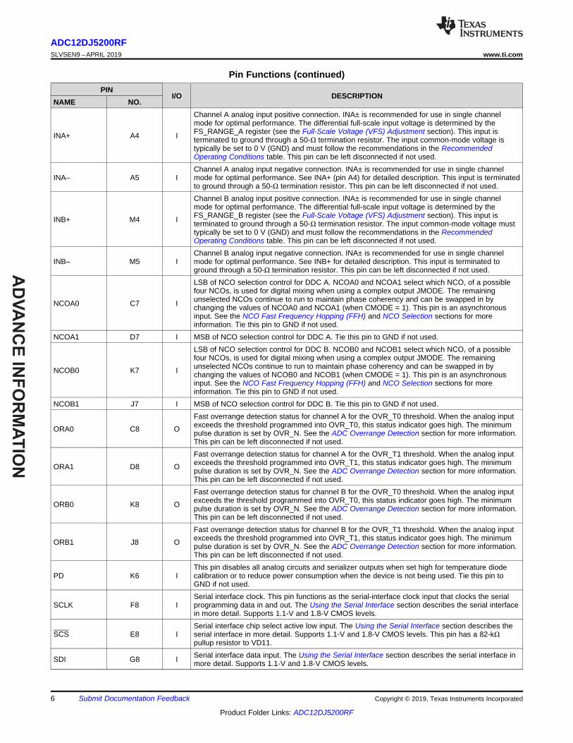
Channel A analog input positive connection. INA± is recommended for use in single channelmode for optimal performance. The differential full-scale input voltage is determined by theFS_RANGE_A register (see the Full-Scale Voltage (VFS) Adjustment section). This input isterminated to ground through a 50-Ω termination resistor. The input common-mode voltage istypically be set to 0 V (GND) and must follow the recommendations in the RecommendedOperating Conditions table. This pin can be left disconnected if not used.
INA– A5 IChannel A analog input negative connection. INA± is recommended for use in single channelmode for optimal performance. See INA+ (pin A4) for detailed description. This input is terminatedto ground through a 50-Ω termination resistor. This pin can be left disconnected if not used.
INB+ M4 I
Channel B analog input positive connection. INA± is recommended for use in single channelmode for optimal performance. The differential full-scale input voltage is determined by theFS_RANGE_B register (see the Full-Scale Voltage (VFS) Adjustment section). This input isterminated to ground through a 50-Ω termination resistor. The input common-mode voltage musttypically be set to 0 V (GND) and must follow the recommendations in the RecommendedOperating Conditions table. This pin can be left disconnected if not used.
INB– M5 IChannel B analog input negative connection. INA± is recommended for use in single channelmode for optimal performance. See INB+ for detailed description. This input is terminated toground through a 50-Ω termination resistor. This pin can be left disconnected if not used.
NCOA0 C7 I
LSB of NCO selection control for DDC A. NCOA0 and NCOA1 select which NCO, of a possiblefour NCOs, is used for digital mixing when using a complex output JMODE. The remainingunselected NCOs continue to run to maintain phase coherency and can be swapped in bychanging the values of NCOA0 and NCOA1 (when CMODE = 1). This pin is an asynchronousinput. See the NCO Fast Frequency Hopping (FFH) and NCO Selection sections for moreinformation. Tie this pin to GND if not used.
NCOA1 D7 I MSB of NCO selection control for DDC A. Tie this pin to GND if not used.
NCOB0 K7 I
LSB of NCO selection control for DDC B. NCOB0 and NCOB1 select which NCO, of a possiblefour NCOs, is used for digital mixing when using a complex output JMODE. The remainingunselected NCOs continue to run to maintain phase coherency and can be swapped in bychanging the values of NCOB0 and NCOB1 (when CMODE = 1). This pin is an asynchronousinput. See the NCO Fast Frequency Hopping (FFH) and NCO Selection sections for moreinformation. Tie this pin to GND if not used.
NCOB1 J7 I MSB of NCO selection control for DDC B. Tie this pin to GND if not used.
ORA0 C8 O
Fast overrange detection status for channel A for the OVR_T0 threshold. When the analog inputexceeds the threshold programmed into OVR_T0, this status indicator goes high. The minimumpulse duration is set by OVR_N. See the ADC Overrange Detection section for more information.This pin can be left disconnected if not used.
ORA1 D8 O
Fast overrange detection status for channel A for the OVR_T1 threshold. When the analog inputexceeds the threshold programmed into OVR_T1, this status indicator goes high. The minimumpulse duration is set by OVR_N. See the ADC Overrange Detection section for more information.This pin can be left disconnected if not used.
ORB0 K8 O
Fast overrange detection status for channel B for the OVR_T0 threshold. When the analog inputexceeds the threshold programmed into OVR_T0, this status indicator goes high. The minimumpulse duration is set by OVR_N. See the ADC Overrange Detection section for more information.This pin can be left disconnected if not used.
ORB1 J8 O
Fast overrange detection status for channel B for the OVR_T1 threshold. When the analog inputexceeds the threshold programmed into OVR_T1, this status indicator goes high. The minimumpulse duration is set by OVR_N. See the ADC Overrange Detection section for more information.This pin can be left disconnected if not used.
PD K6 IThis pin disables all analog circuits and serializer outputs when set high for temperature diodecalibration or to reduce power consumption when the device is not being used. Tie this pin toGND if not used.
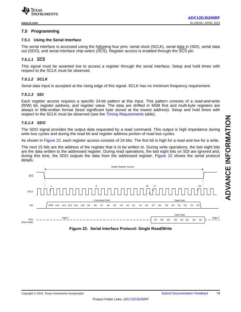
SCLK F8 ISerial interface clock. This pin functions as the serial-interface clock input that clocks the serialprogramming data in and out. The Using the Serial Interface section describes the serial interfacein more detail. Supports 1.1-V and 1.8-V CMOS levels.
SCS E8 ISerial interface chip select active low input. The Using the Serial Interface section describes theserial interface in more detail. Supports 1.1-V and 1.8-V CMOS levels. This pin has a 82-kΩpullup resistor to VD11.
SDI G8 I Serial interface data input. The Using the Serial Interface section describes the serial interface inmore detail. Supports 1.1-V and 1.8-V CMOS levels.
SDO H8 OSerial interface data output. The Using the Serial Interface section describes the serial interfacein more detail. This pin is high impedance during normal device operation. This pin outputs 1.9-VCMOS levels during serial interface read operations. This pin can be left disconnected if not used.
SYNCSE C2 I
Single-ended JESD204C SYNC signal. This input is an active low input that is used to initializethe JESD204C serial link in 8B/10B modes when SYNC_SEL is set to 0. The 64B/66B modes donot use the SYNC signal for initialization, however it may be used for NCO synchronization.When toggled low in 8B/10B modes this input initiates code group synchronization (see the CodeGroup Synchronization (CGS) section). After code group synchronization, this input must betoggled high to start the initial lane alignment sequence (see the Initial Lane Alignment Sequence(ILAS) section). A differential SYNC signal can be used instead by setting SYNC_SEL to 1 andusing TMSTP± as a differential SYNC input. Tie this pin to GND if differential SYNC (TMSTP±) isused as the JESD204C SYNC signal.
SYSREF+ K1 I
The SYSREF positive input is used to achieve synchronization and deterministic latency acrossthe JESD204C interface. This differential input (SYSREF+ to SYSREF–) has an internaluntrimmed 100-Ω differential termination and can be AC-coupled when SYSREF_LVPECL_EN isset to 0. This input is self-biased when SYSREF_LVPECL_EN is set to 0. The terminationchanges to 50 Ω to ground on each input pin (SYSREF+ and SYSREF–) and can be DC-coupledwhen SYSREF_LVPECL_EN is set to 1. This input is not self-biased whenSYSREF_LVPECL_EN is set to 1 and must be biased externally to the input common-modevoltage range provided in the Recommended Operating Conditions table.
SYSREF– L1 I SYSREF negative input
TDIODE+ K2 ITemperature diode positive (anode) connection. An external temperature sensor can beconnected to TDIODE+ and TDIODE– to monitor the junction temperature of the device. This pincan be left disconnected if not used.
TDIODE– K3 I Temperature diode negative (cathode) connection. This pin can be left disconnected if not used.
TMSTP+ B1 I
Timestamp input positive connection or differential JESD204C SYNC positive connection. Thisinput is a timestamp input, used to mark a specific sample, when TIMESTAMP_EN is set to 1.This differential input is used as the JESD204C SYNC signal input when SYNC_SEL is set 1.This input can be used as both a timestamp and differential SYNC input at the same time,allowing feedback of the SYNC signal using the timestamp mechanism. TMSTP± uses active lowsignaling when used as a JESD204C SYNC. For additional usage information, see theTimestamp section.TMSTP_RECV_EN must be set to 1 to use this input. This differential input (TMSTP+ toTMSTP–) has an internal untrimmed 100-Ω differential termination and can be AC-coupled whenTMSTP_LVPECL_EN is set to 0. The termination changes to 50 Ω to ground on each input pin(TMSTP+ and TMSTP–) and can be DC coupled when TMSTP_LVPECL_EN is set to 1. This pinis not self-biased and therefore must be externally biased for both AC- and DC-coupledconfigurations. The common-mode voltage must be within the range provided in theRecommended Operating Conditions table when both AC and DC coupled. This pin can be leftdisconnected and disabled (TMSTP_RECV_EN = 0) if SYNCSE is used for JESD204C SYNCand timestamp is not required.
TMSTP– C1 ITimestamp input positive connection or differential JESD204C SYNC negative connection. Thispin can be left disconnected and disabled (TMSTP_RECV_EN = 0) if SYNCSE is used forJESD204C SYNC and timestamp is not required.
(1) Stresses beyond those listed under Absolute Maximum Ratings may cause permanent damage to the device. These are stress ratingsonly, which do not imply functional operation of the device at these or any other conditions beyond those indicated under RecommendedOperating Conditions. Exposure to absolute-maximum-rated conditions for extended periods may affect device reliability.
(2) Measured to AGND.(3) Measured to DGND.(4) Maximum voltage not to exceed VD11 absolute maximum rating.(5) Maximum voltage not to exceed VA11 absolute maximum rating.(6) Maximum voltage not to exceed VA19 absolute maximum rating.
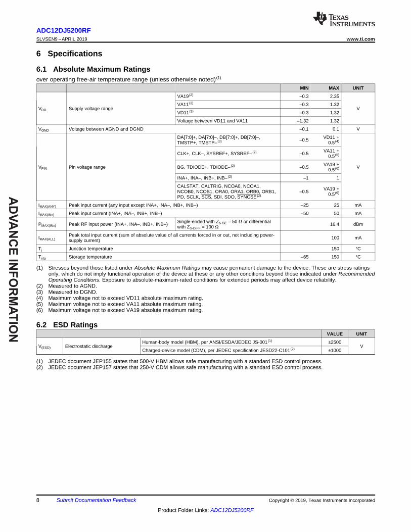
6 Specifications
6.1 Absolute Maximum Ratingsover operating free-air temperature range (unless otherwise noted) (1)
IMAX(ANY) Peak input current (any input except INA+, INA–, INB+, INB–) –25 25 mA
IMAX(INx) Peak input current (INA+, INA–, INB+, INB–) –50 50 mA
PMAX(INx) Peak RF input power (INA+, INA–, INB+, INB–) Single-ended with ZS-SE = 50 Ω or differentialwith ZS-DIFF = 100 Ω 16.4 dBm
IMAX(ALL)Peak total input current (sum of absolute value of all currents forced in or out, not including power-supply current) 100 mA
Tj Junction temperature 150 °C
Tstg Storage temperature –65 150 °C
(1) JEDEC document JEP155 states that 500-V HBM allows safe manufacturing with a standard ESD control process.(2) JEDEC document JEP157 states that 250-V CDM allows safe manufacturing with a standard ESD control process.
6.2 ESD RatingsVALUE UNIT
V(ESD) Electrostatic dischargeHuman-body model (HBM), per ANSI/ESDA/JEDEC JS-001 (1) ±2500
VCharged-device model (CDM), per JEDEC specification JESD22-C101 (2) ±1000
(1) Measured to AGND.(2) Measured to DGND.(3) TI strongly recommends that CLK± be AC-coupled with DEVCLK_LVPECL_EN set to 0 to allow CLK± to self-bias to the optimal input
common-mode voltage for best performance. TI recommends AC-coupling for SYSREF± unless DC-coupling is required, in which case,the LVPECL input mode must be used (SYSREF_LVPECL_EN = 1).
(4) TMSTP± does not have internal biasing that requires TMSTP± to be biased externally whether AC-coupled with TMSTP_LVPECL_EN =0 or DC-coupled with TMSTP_LVPECL_EN= 1.
(5) The ADC output code saturates when VID for INA± or INB± exceeds the programmed full-scale voltage(VFS) set by FS_RANGE_A forINA± or FS_RANGE_B for INB±.
(6) Prolonged use above junction temperature of 105°C may increase the device failure-in-time (FIT) rate.
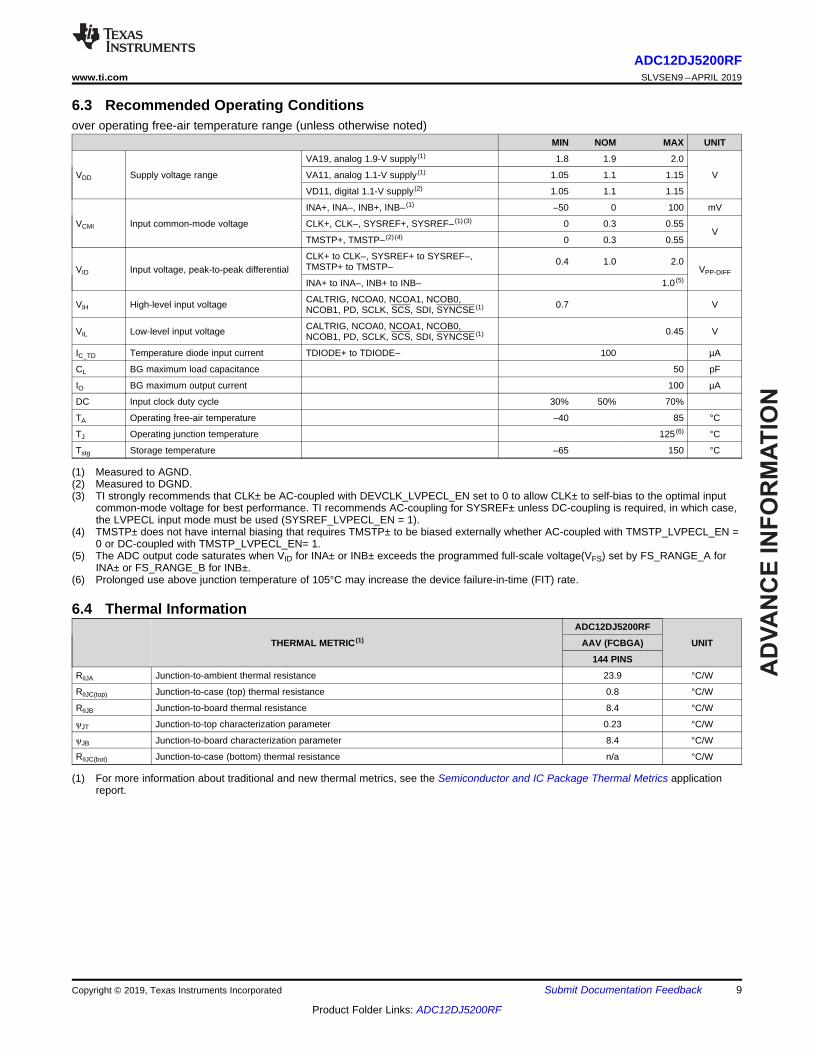
6.3 Recommended Operating Conditionsover operating free-air temperature range (unless otherwise noted)
MIN NOM MAX UNIT
VDD Supply voltage range
VA19, analog 1.9-V supply (1) 1.8 1.9 2.0
VVA11, analog 1.1-V supply (1) 1.05 1.1 1.15
VD11, digital 1.1-V supply (2) 1.05 1.1 1.15
VCMI Input common-mode voltage
INA+, INA–, INB+, INB– (1) –50 0 100 mV
CLK+, CLK–, SYSREF+, SYSREF– (1) (3) 0 0.3 0.55V
TMSTP+, TMSTP– (2) (4) 0 0.3 0.55
VID Input voltage, peak-to-peak differentialCLK+ to CLK–, SYSREF+ to SYSREF–,TMSTP+ to TMSTP– 0.4 1.0 2.0
VPP-DIFF
INA+ to INA–, INB+ to INB– 1.0 (5)
VIH High-level input voltage CALTRIG, NCOA0, NCOA1, NCOB0,NCOB1, PD, SCLK, SCS, SDI, SYNCSE (1) 0.7 V
VIL Low-level input voltage CALTRIG, NCOA0, NCOA1, NCOB0,NCOB1, PD, SCLK, SCS, SDI, SYNCSE (1) 0.45 V
IC_TD Temperature diode input current TDIODE+ to TDIODE– 100 µA
CL BG maximum load capacitance 50 pF
IO BG maximum output current 100 µA
DC Input clock duty cycle 30% 50% 70%
TA Operating free-air temperature –40 85 °C
TJ Operating junction temperature 125 (6) °C
Tstg Storage temperature –65 150 °C
(1) For more information about traditional and new thermal metrics, see the Semiconductor and IC Package Thermal Metrics applicationreport.
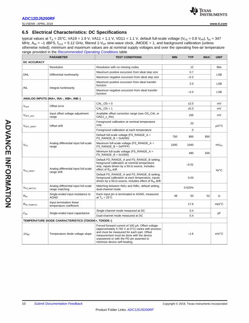
6.5 Electrical Characteristics: DC Specificationstypical values at TA = 25°C, VA19 = 1.9 V, VA11 = 1.1 V, VD11 = 1.1 V, default full-scale voltage (VFS = 0.8 VPP), fIN = 347MHz, AIN = –1 dBFS, fCLK = 5.12 GHz, filtered 1-VPP sine-wave clock, JMODE = 1, and background calibration (unlessotherwise noted); minimum and maximum values are at nominal supply voltages and over the operating free-air temperaturerange provided in the Recommended Operating Conditions table
PARAMETER TEST CONDITIONS MIN TYP MAX UNIT
DC ACCURACY
Resolution Resolution with no missing codes 12 Bits
DNL Differential nonlinearityMaximum positive excursion from ideal step size 0.7
LSBMaximum negative excursion from ideal step size –0.3
INL Integral nonlinearity
Maximum positive excursion from ideal transferfunction 2.0 LSB
Maximum negative excursion from ideal transferfunction –2.0 LSB
ANALOG INPUTS (INA+, INA–, INB+, INB–)
VOFF Offset errorCAL_OS = 0 ±2.0 mV
CAL_OS = 1 ±0.3 mV
VOFF_ADJInput offset voltage adjustmentrange
Available offset correction range (see OS_CAL orOADJ_x_INx) ±55 mV
VOFF_DRIFT Offset driftForeground calibration at nominal temperatureonly 23
µV/°CForeground calibration at each temperature 0
VFSAnalog differential input full-scalerange
Default full-scale voltage (FS_RANGE_A =FS_RANGE_B = 0xA000) 750 800 850
mVPPMaximum full-scale voltage (FS_RANGE_A =FS_RANGE_B = 0xFFFF) 1000 1040
Minimum full-scale voltage (FS_RANGE_A =FS_RANGE_B = 0x2000) 480 500
Default FS_RANGE_A and FS_RANGE_B setting,foreground calibration at nominal temperatureonly, inputs driven by a 50-Ω source, includeseffect of RIN drift
–0.01
%/°CDefault FS_RANGE_A and FS_RANGE_B setting,foreground calibration at each temperature, inputsdriven by a 50-Ω source, includes effect of RIN drift
CIN Single-ended input capacitanceSingle-channel mode measured at DC 0.4
pFDual-channel mode measured at DC 0.4
TEMPERATURE DIODE CHARACTERISTICS (TDIODE+, TDIODE–)
ΔVBE Temperature diode voltage slope
Forced forward current of 100 µA. Offset voltage(approximately 0.792 V at 0°C) varies with processand must be measured for each part. Offsetmeasurement must be done with the deviceunpowered or with the PD pin asserted tominimize device self-heating.
Electrical Characteristics: DC Specifications (continued)typical values at TA = 25°C, VA19 = 1.9 V, VA11 = 1.1 V, VD11 = 1.1 V, default full-scale voltage (VFS = 0.8 VPP), fIN = 347MHz, AIN = –1 dBFS, fCLK = 5.12 GHz, filtered 1-VPP sine-wave clock, JMODE = 1, and background calibration (unlessotherwise noted); minimum and maximum values are at nominal supply voltages and over the operating free-air temperaturerange provided in the Recommended Operating Conditions table
PARAMETER TEST CONDITIONS MIN TYP MAX UNIT
BAND-GAP VOLTAGE OUTPUT (BG)
VBG Reference output voltage IL ≤ 100 µA 1.1 V
VBG_DRIFT Reference output temperature drift IL ≤ 100 µA –64 µV/°C
6.6 Electrical Characteristics: Power Consumptiontypical values at TA = 25°C, VA19 = 1.9 V, VA11 = 1.1 V, VD11 = 1.1 V, default full-scale voltage (VFS = 0.8 VPP), fIN = 347MHz, AIN = –1 dBFS, fCLK = 5.12 GHz, filtered 1-VPP sine-wave clock, JMODE = 1, and background calibration (unlessotherwise noted); minimum and maximum values are at nominal supply voltages and over the operating free-air temperaturerange provided in the Recommended Operating Conditions table
(1) Full-power input bandwidth (FPBW) is defined as the input frequency where the reconstructed output of the ADC has dropped 3 dBbelow the power of a full-scale input signal at a low input frequency. Useable bandwidth may exceed the –3-dB, full-power inputbandwidth.
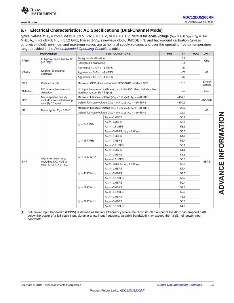
6.7 Electrical Characteristics: AC Specifications (Dual-Channel Mode)typical values at TA = 25°C, VA19 = 1.9 V, VA11 = 1.1 V, VD11 = 1.1 V, default full-scale voltage (VFS = 0.8 VPP), fIN = 347MHz, AIN = –1 dBFS, fCLK = 5.12 GHz, filtered 1-VPP sine-wave clock, JMODE = 3, and background calibration (unlessotherwise noted); minimum and maximum values are at nominal supply voltages and over the operating free-air temperaturerange provided in the Recommended Operating Conditions table
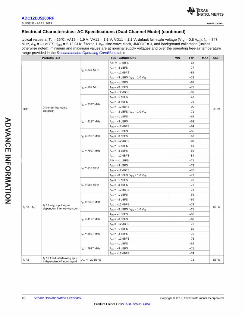
PARAMETER TEST CONDITIONS MIN TYP MAX UNIT
FPBW Full-power input bandwidth(–3 dB) (1)
Foreground calibration 8.1GHz
Background calibration 8.1
XTALK Channel-to-channelcrosstalk
Aggressor = 1 GHz, –1 dBFS –87
dBAggressor = 3 GHz, –1 dBFS –76
Aggressor = 6 GHz, –1 dBFS –62
CER Code error rate Maximum CER, does not include JESD204C interface BER 10–18 Errors/sample
NOISEDCDC input noise standarddeviation
No input, foreground calibration, excludes DC offset, includes fixedinterleaving spur (fS / 2 spur) 2.3 LSB
Electrical Characteristics: AC Specifications (Dual-Channel Mode) (continued)typical values at TA = 25°C, VA19 = 1.9 V, VA11 = 1.1 V, VD11 = 1.1 V, default full-scale voltage (VFS = 0.8 VPP), fIN = 347MHz, AIN = –1 dBFS, fCLK = 5.12 GHz, filtered 1-VPP sine-wave clock, JMODE = 3, and background calibration (unlessotherwise noted); minimum and maximum values are at nominal supply voltages and over the operating free-air temperaturerange provided in the Recommended Operating Conditions table
PARAMETER TEST CONDITIONS MIN TYP MAX UNIT
SINADSignal-to-noise anddistortion ratio, excludingDC and fS / 2 fixed spurs
fIN = 347 MHz
AIN = –1 dBFS 54.4
dBFS
AIN = –3 dBFS 55.3
AIN = –12 dBFS 56.0
AIN = –3 dBFS, VFS = 1.0 VPP 56.0
fIN = 997 MHz
AIN = –1 dBFS 54.2
AIN = –3 dBFS 54.8
AIN = –12 dBFS 55.8
fIN = 2397 MHz
AIN = –1 dBFS 53.4
AIN = –3 dBFS 54.3
AIN = –12 dBFS 55.9
AIN = –3 dBFS, VFS = 1.0 VPP 55.1
fIN = 4197 MHz
AIN = –1 dBFS 51.3
AIN = –3 dBFS 52.7
AIN = –12 dBFS 55.5
fIN = 5997 MHz
AIN = –1 dBFS 48.6
AIN = –3 dBFS 51.0
AIN = –12 dBFS 55.2
fIN = 7997 MHz
AIN = –1 dBFS 46.2
AIN = –3 dBFS 48.9
AIN = –12 dBFS 54.7
ENOBEffective number of bits,excluding DC and fS / 2fixed spurs
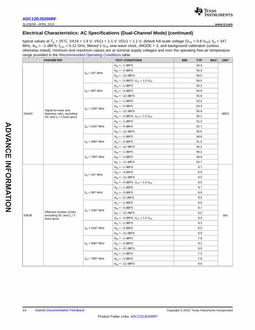
Electrical Characteristics: AC Specifications (Dual-Channel Mode) (continued)typical values at TA = 25°C, VA19 = 1.9 V, VA11 = 1.1 V, VD11 = 1.1 V, default full-scale voltage (VFS = 0.8 VPP), fIN = 347MHz, AIN = –1 dBFS, fCLK = 5.12 GHz, filtered 1-VPP sine-wave clock, JMODE = 3, and background calibration (unlessotherwise noted); minimum and maximum values are at nominal supply voltages and over the operating free-air temperaturerange provided in the Recommended Operating Conditions table
PARAMETER TEST CONDITIONS MIN TYP MAX UNIT
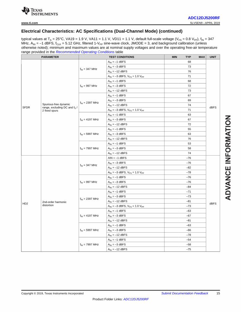
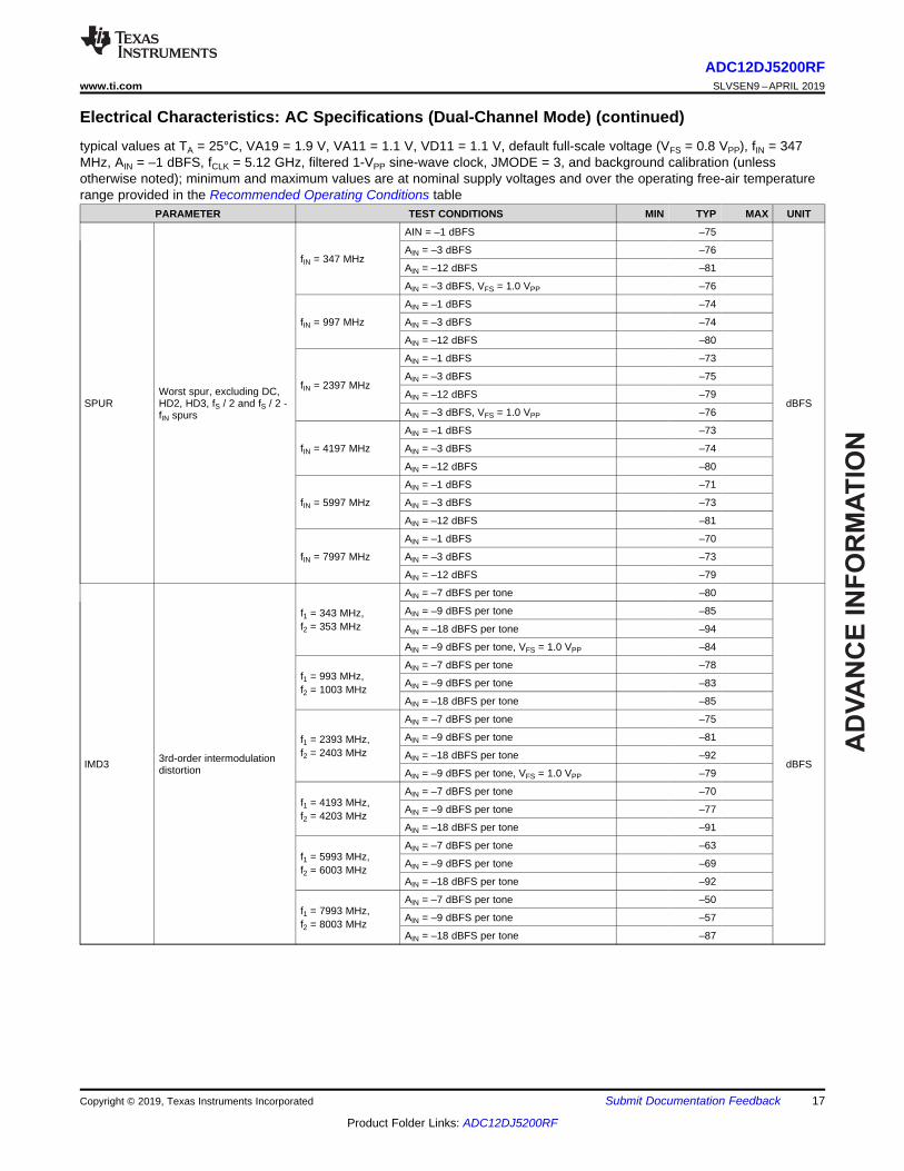
SFDRSpurious-free dynamicrange, excluding DC and fS /2 fixed spurs
Electrical Characteristics: AC Specifications (Dual-Channel Mode) (continued)typical values at TA = 25°C, VA19 = 1.9 V, VA11 = 1.1 V, VD11 = 1.1 V, default full-scale voltage (VFS = 0.8 VPP), fIN = 347MHz, AIN = –1 dBFS, fCLK = 5.12 GHz, filtered 1-VPP sine-wave clock, JMODE = 3, and background calibration (unlessotherwise noted); minimum and maximum values are at nominal supply voltages and over the operating free-air temperaturerange provided in the Recommended Operating Conditions table
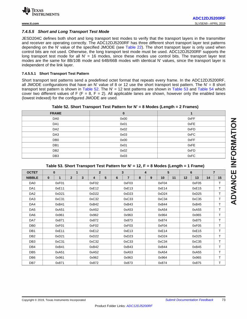
Electrical Characteristics: AC Specifications (Dual-Channel Mode) (continued)typical values at TA = 25°C, VA19 = 1.9 V, VA11 = 1.1 V, VD11 = 1.1 V, default full-scale voltage (VFS = 0.8 VPP), fIN = 347MHz, AIN = –1 dBFS, fCLK = 5.12 GHz, filtered 1-VPP sine-wave clock, JMODE = 3, and background calibration (unlessotherwise noted); minimum and maximum values are at nominal supply voltages and over the operating free-air temperaturerange provided in the Recommended Operating Conditions table
(1) Full-power input bandwidth (FPBW) is defined as the input frequency where the reconstructed output of the ADC has dropped 3 dBbelow the power of a full-scale input signal at a low input frequency. Useable bandwidth may exceed the –3-dB, full-power inputbandwidth.
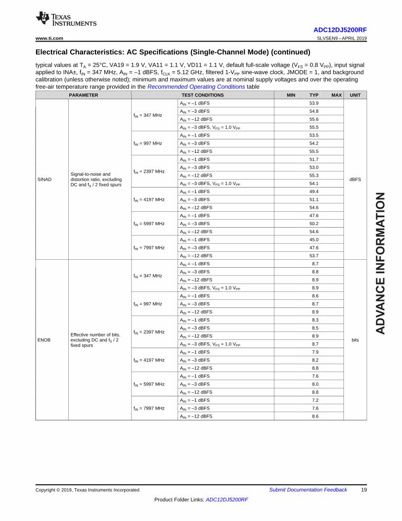
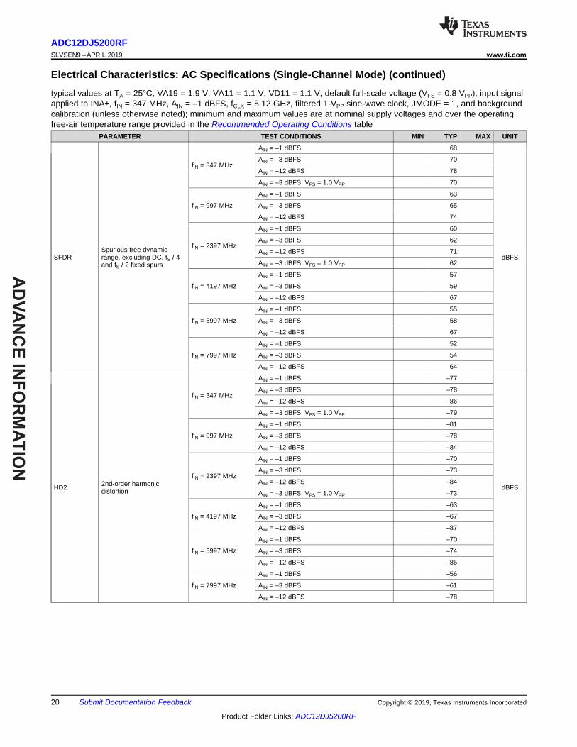
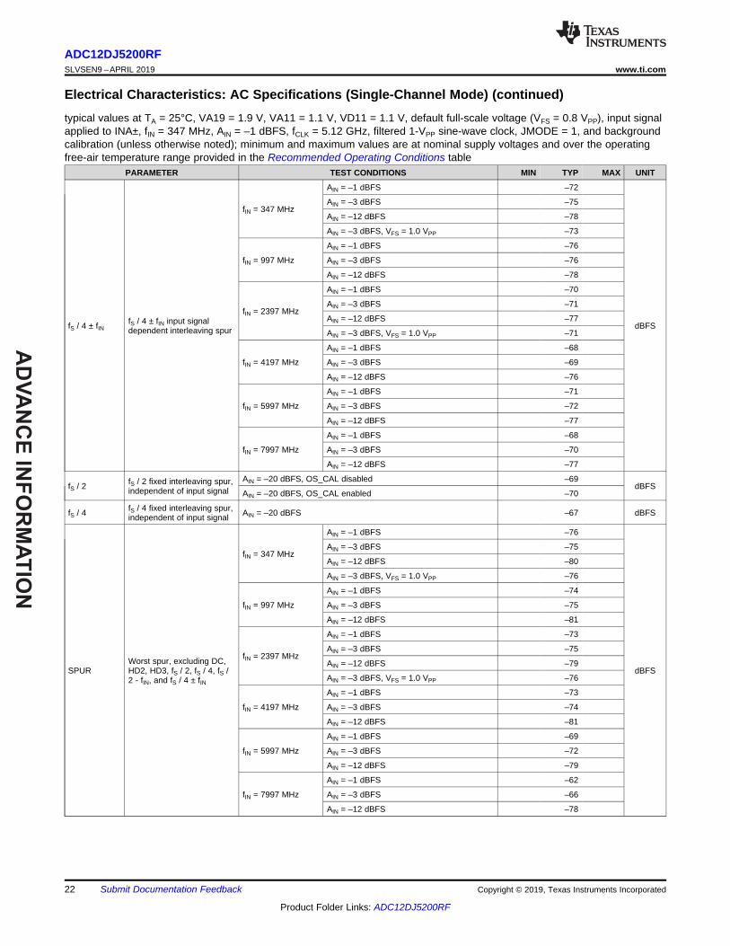
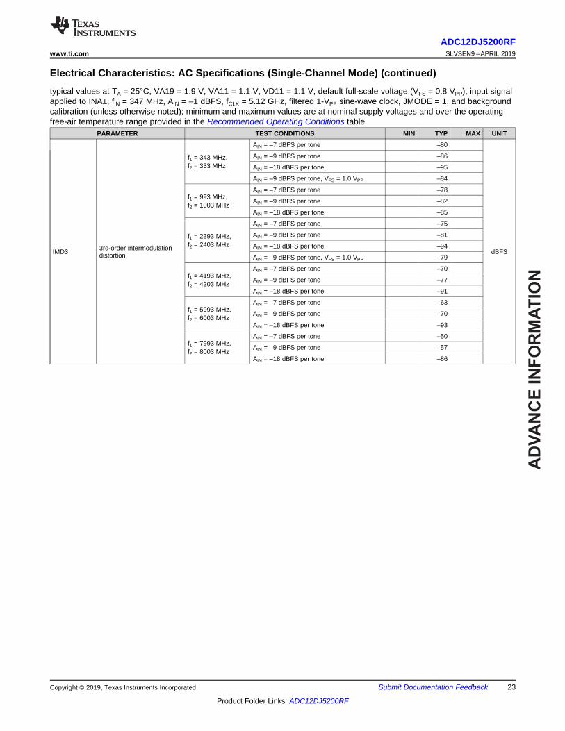
6.8 Electrical Characteristics: AC Specifications (Single-Channel Mode)typical values at TA = 25°C, VA19 = 1.9 V, VA11 = 1.1 V, VD11 = 1.1 V, default full-scale voltage (VFS = 0.8 VPP), input signalapplied to INA±, fIN = 347 MHz, AIN = –1 dBFS, fCLK = 5.12 GHz, filtered 1-VPP sine-wave clock, JMODE = 1, and backgroundcalibration (unless otherwise noted); minimum and maximum values are at nominal supply voltages and over the operatingfree-air temperature range provided in the Recommended Operating Conditions table
PARAMETER TEST CONDITIONS MIN TYP MAX UNIT
FPBW Full-power input bandwidth(–3 dB) (1)
Foreground calibration 7.9GHz
Background calibration 7.9
CER Code error rate Maximum CER, does not include JESD204C interface BER 10–18 Errors/sample
NOISEDCDC input noise standarddeviation
No input, foreground calibration, excludes DC offset, includes fixedinterleaving spurs (fS / 2 and fS / 4 spurs), OS_CAL enabled 2.7 LSB
Electrical Characteristics: AC Specifications (Single-Channel Mode) (continued)typical values at TA = 25°C, VA19 = 1.9 V, VA11 = 1.1 V, VD11 = 1.1 V, default full-scale voltage (VFS = 0.8 VPP), input signalapplied to INA±, fIN = 347 MHz, AIN = –1 dBFS, fCLK = 5.12 GHz, filtered 1-VPP sine-wave clock, JMODE = 1, and backgroundcalibration (unless otherwise noted); minimum and maximum values are at nominal supply voltages and over the operatingfree-air temperature range provided in the Recommended Operating Conditions table
PARAMETER TEST CONDITIONS MIN TYP MAX UNIT
SINADSignal-to-noise anddistortion ratio, excludingDC and fS / 2 fixed spurs
fIN = 347 MHz
AIN = –1 dBFS 53.9
dBFS
AIN = –3 dBFS 54.8
AIN = –12 dBFS 55.6
AIN = –3 dBFS, VFS = 1.0 VPP 55.5
fIN = 997 MHz
AIN = –1 dBFS 53.5
AIN = –3 dBFS 54.2
AIN = –12 dBFS 55.5
fIN = 2397 MHz
AIN = –1 dBFS 51.7
AIN = –3 dBFS 53.0
AIN = –12 dBFS 55.3
AIN = –3 dBFS, VFS = 1.0 VPP 54.1
fIN = 4197 MHz
AIN = –1 dBFS 49.4
AIN = –3 dBFS 51.1
AIN = –12 dBFS 54.6
fIN = 5997 MHz
AIN = –1 dBFS 47.6
AIN = –3 dBFS 50.2
AIN = –12 dBFS 54.6
fIN = 7997 MHz
AIN = –1 dBFS 45.0
AIN = –3 dBFS 47.6
AIN = –12 dBFS 53.7
ENOBEffective number of bits,excluding DC and fS / 2fixed spurs
Electrical Characteristics: AC Specifications (Single-Channel Mode) (continued)typical values at TA = 25°C, VA19 = 1.9 V, VA11 = 1.1 V, VD11 = 1.1 V, default full-scale voltage (VFS = 0.8 VPP), input signalapplied to INA±, fIN = 347 MHz, AIN = –1 dBFS, fCLK = 5.12 GHz, filtered 1-VPP sine-wave clock, JMODE = 1, and backgroundcalibration (unless otherwise noted); minimum and maximum values are at nominal supply voltages and over the operatingfree-air temperature range provided in the Recommended Operating Conditions table
Electrical Characteristics: AC Specifications (Single-Channel Mode) (continued)typical values at TA = 25°C, VA19 = 1.9 V, VA11 = 1.1 V, VD11 = 1.1 V, default full-scale voltage (VFS = 0.8 VPP), input signalapplied to INA±, fIN = 347 MHz, AIN = –1 dBFS, fCLK = 5.12 GHz, filtered 1-VPP sine-wave clock, JMODE = 1, and backgroundcalibration (unless otherwise noted); minimum and maximum values are at nominal supply voltages and over the operatingfree-air temperature range provided in the Recommended Operating Conditions table
Electrical Characteristics: AC Specifications (Single-Channel Mode) (continued)typical values at TA = 25°C, VA19 = 1.9 V, VA11 = 1.1 V, VD11 = 1.1 V, default full-scale voltage (VFS = 0.8 VPP), input signalapplied to INA±, fIN = 347 MHz, AIN = –1 dBFS, fCLK = 5.12 GHz, filtered 1-VPP sine-wave clock, JMODE = 1, and backgroundcalibration (unless otherwise noted); minimum and maximum values are at nominal supply voltages and over the operatingfree-air temperature range provided in the Recommended Operating Conditions table
Electrical Characteristics: AC Specifications (Single-Channel Mode) (continued)typical values at TA = 25°C, VA19 = 1.9 V, VA11 = 1.1 V, VD11 = 1.1 V, default full-scale voltage (VFS = 0.8 VPP), input signalapplied to INA±, fIN = 347 MHz, AIN = –1 dBFS, fCLK = 5.12 GHz, filtered 1-VPP sine-wave clock, JMODE = 1, and backgroundcalibration (unless otherwise noted); minimum and maximum values are at nominal supply voltages and over the operatingfree-air temperature range provided in the Recommended Operating Conditions table
(1) Unless functionally limited to a smaller range in the ADC12DJ5200RF Operating Modes table based on programmed JMODE.(2) Use SYSREF_POS to select an optimal SYSREF_SEL value for the SYSREF capture, see the SYSREF Position Detector and
Sampling Position Selection (SYSREF Windowing) section for more information on SYSREF windowing. The invalid region, specified bytINV(SYSREF), indicates the portion of the CLK± period(tCLK), as measured by SYSREF_SEL, that may result in a setup and hold violation.Verify that the timing skew between SYSREF± and CLK± over system operating conditions from the nominal conditions (that used tofind optimal SYSREF_SEL) does not result in the invalid region occurring at the selected SYSREF_SEL position in SYSREF_POS,otherwise a temperature dependent SYSREF_SEL selection may be needed to track the skew between CLK± and SYSREF±.
(3) This parameter only applies to JMODE settings that use 8B/10B encoding or settings that use 64B/66B encoding and 4x or 8xdecimation. SYNC is not used for 64B/66B encoding modes unless the DDC block and NCOs are used and require synchronization.
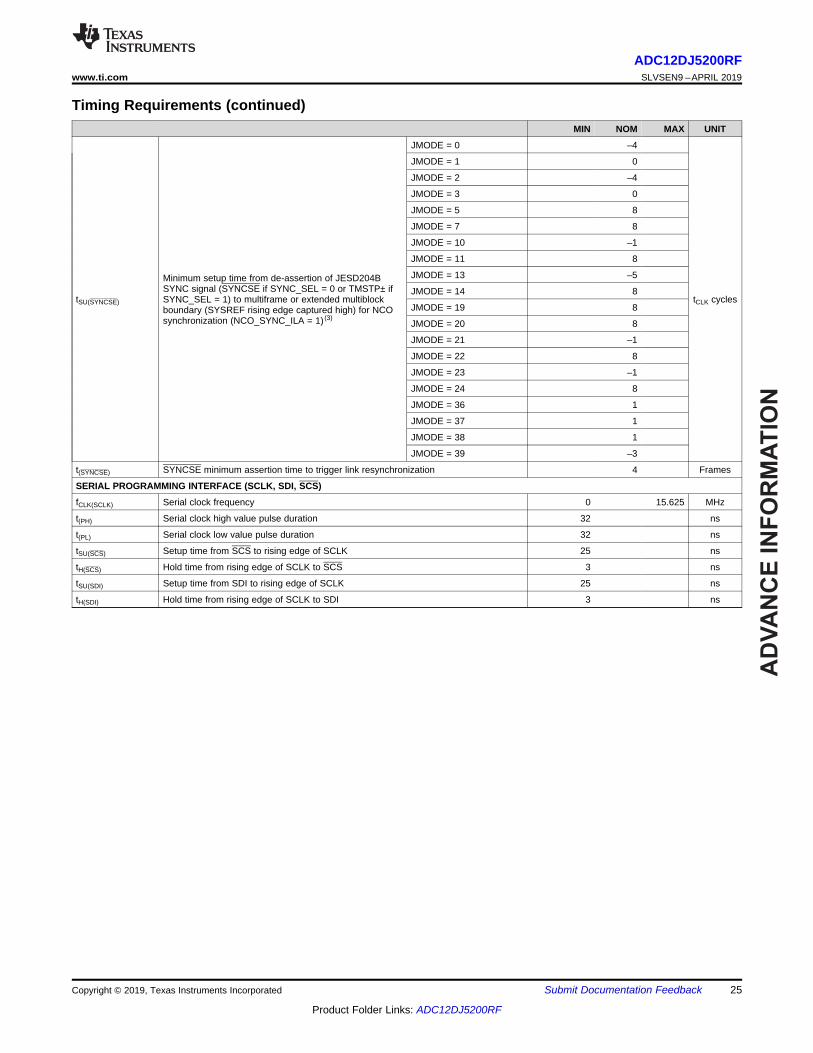
6.9 Timing RequirementsMIN NOM MAX UNIT
DEVICE (SAMPLING) CLOCK (CLK+, CLK–)
fCLK Input clock frequency (CLK±), both single-channel and dual-channel modes (1) 800 5200 MHz
tCLK Input clock period (CLK±), both single-channel and dual-channel modes (1) 192.3 1250 ps
SYSREF (SYSREF+, SYSREF–)
tINV(SYSREF)Width of invalid SYSREF capture region of CLK± period, indicating setup or hold timeviolation, as measured by SYSREF_POS status register (2) 48 ps
tINV(TEMP)Drift of invalid SYSREF capture region over temperature, positive number indicates ashift toward MSB of SYSREF_POS register 0 ps/°C
tINV(VA11)Drift of invalid SYSREF capture region over VA11 supply voltage, positive numberindicates a shift toward MSB of SYSREF_POS register 0.36 ps/mV
tSTEP(SP) Delay of SYSREF_POS LSBSYSREF_ZOOM = 0 77
Minimum hold time from multiframe or extendedmultiblock boundary (SYSREF rising edge captured high)to de-assertion of JESD204B SYNC signal (SYNCSE ifSYNC_SEL = 0 or TMSTP± if SYNC_SEL = 1) for NCOsynchronization (NCO_SYNC_ILA = 1) (3)
Minimum setup time from de-assertion of JESD204BSYNC signal (SYNCSE if SYNC_SEL = 0 or TMSTP± ifSYNC_SEL = 1) to multiframe or extended multiblockboundary (SYSREF rising edge captured high) for NCOsynchronization (NCO_SYNC_ILA = 1) (3)
JMODE = 0 –4
tCLK cycles
JMODE = 1 0
JMODE = 2 –4
JMODE = 3 0
JMODE = 5 8
JMODE = 7 8
JMODE = 10 –1
JMODE = 11 8
JMODE = 13 –5
JMODE = 14 8
JMODE = 19 8
JMODE = 20 8
JMODE = 21 –1
JMODE = 22 8
JMODE = 23 –1
JMODE = 24 8
JMODE = 36 1
JMODE = 37 1
JMODE = 38 1
JMODE = 39 –3
t(SYNCSE) SYNCSE minimum assertion time to trigger link resynchronization 4 Frames
SERIAL PROGRAMMING INTERFACE (SCLK, SDI, SCS)
fCLK(SCLK) Serial clock frequency 0 15.625 MHz
t(PH) Serial clock high value pulse duration 32 ns
t(PL) Serial clock low value pulse duration 32 ns
tSU(SCS) Setup time from SCS to rising edge of SCLK 25 ns
tH(SCS) Hold time from rising edge of SCLK to SCS 3 ns
tSU(SDI) Setup time from SDI to rising edge of SCLK 25 ns
tH(SDI) Hold time from rising edge of SCLK to SDI 3 ns
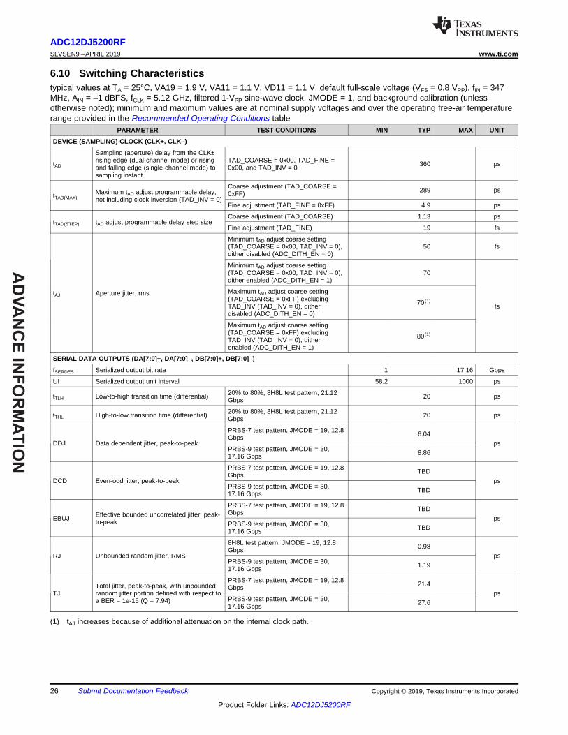
(1) tAJ increases because of additional attenuation on the internal clock path.
6.10 Switching Characteristicstypical values at TA = 25°C, VA19 = 1.9 V, VA11 = 1.1 V, VD11 = 1.1 V, default full-scale voltage (VFS = 0.8 VPP), fIN = 347MHz, AIN = –1 dBFS, fCLK = 5.12 GHz, filtered 1-VPP sine-wave clock, JMODE = 1, and background calibration (unlessotherwise noted); minimum and maximum values are at nominal supply voltages and over the operating free-air temperaturerange provided in the Recommended Operating Conditions table
PARAMETER TEST CONDITIONS MIN TYP MAX UNIT
DEVICE (SAMPLING) CLOCK (CLK+, CLK–)
tAD
Sampling (aperture) delay from the CLK±rising edge (dual-channel mode) or risingand falling edge (single-channel mode) tosampling instant
Switching Characteristics (continued)typical values at TA = 25°C, VA19 = 1.9 V, VA11 = 1.1 V, VD11 = 1.1 V, default full-scale voltage (VFS = 0.8 VPP), fIN = 347MHz, AIN = –1 dBFS, fCLK = 5.12 GHz, filtered 1-VPP sine-wave clock, JMODE = 1, and background calibration (unlessotherwise noted); minimum and maximum values are at nominal supply voltages and over the operating free-air temperaturerange provided in the Recommended Operating Conditions table
PARAMETER TEST CONDITIONS MIN TYP MAX UNIT
(2) tADC is an exact, unrounded, deterministic delay. The delay can be negative if the reference sample is sampled after the SYSREF highcapture point, in which case the total latency is smaller than the delay given by tTX.
ADC CORE LATENCY
tADC
Deterministic delay from the CLK± edgethat samples the reference sample to theCLK± edge that samples SYSREF goinghigh (2)
Switching Characteristics (continued)typical values at TA = 25°C, VA19 = 1.9 V, VA11 = 1.1 V, VD11 = 1.1 V, default full-scale voltage (VFS = 0.8 VPP), fIN = 347MHz, AIN = –1 dBFS, fCLK = 5.12 GHz, filtered 1-VPP sine-wave clock, JMODE = 1, and background calibration (unlessotherwise noted); minimum and maximum values are at nominal supply voltages and over the operating free-air temperaturerange provided in the Recommended Operating Conditions table
PARAMETER TEST CONDITIONS MIN TYP MAX UNIT
(3) The values given for tTX include deterministic and non-deterministic delays. Over process, temperature, and voltage, the delay will vary.JESD204B accounts for these variations when operating in subclass-1 mode in order to achieve deterministic latency. Proper receiverRBD values must be chosen such that the elastic buffer release point does not occur within the invalid region of the local multiframeclock (LMFC) cycle.
JESD204C AND SERIALIZER LATENCY
tTX
Delay from the CLK± rising edge thatsamples SYSREF high to the first bit of themultiframe (8B/10B encoding) or extendedmultiblock (64B/66B encoding) on theJESD204C serial output lanecorresponding to the reference sample oftADC
(3)
JMODE = 0 92 111
tCLK cycles
JMODE = 1 159 189
JMODE = 2 93 112
JMODE = 3 159 189
JMODE = 5 143 172
JMODE = 7 143 172
JMODE = 10 85 102
JMODE = 11 143 172
JMODE = 13 85 102
JMODE = 14 143 170
JMODE = 19 143 168
JMODE = 20 143 168
JMODE = 21 84 102
JMODE = 22 143 172
JMODE = 23 84 102
JMODE = 24 143 170
JMODE = 30 114 134
JMODE = 31 115 134
JMODE = 32 102 120
JMODE = 33 103 120
JMODE = 34 102 120
JMODE = 35 103 120
JMODE = 36 102 120
JMODE = 37 103 120
JMODE = 38 102 120
JMODE = 39 103 120
SERIAL PROGRAMMING INTERFACE (SDO)
t(OZD)Delay from the falling edge of the 16th SCLK cycle during read operation for SDOtransition from tri-state to valid data 1 ns
t(ODZ) Delay from the SCS rising edge for SDO transition from valid data to tri-state 10 ns
t(OD) Delay from the falling edge of SCLK during read operation to SDO valid 1 10 ns
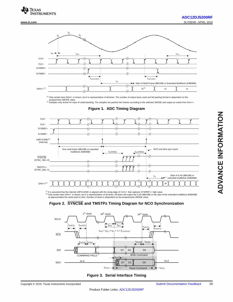
(1) It is assumed that the internal LMFC/LEMC is aligned with the rising edge of CLK+/- that captures SYSREF+/- high value.(2) Only serdes lane DA0+/- is shown, but it is representative of all lanes. All lanes will output the ILAS (8B/10B) or the start of the extended multiblock (64B/66B) at approximately the same point in time. Number of lanes is dependent on the programmed JMODE value.
SYNCSE(SYNC_SEL=0)
tH(SYNCSE) tSU(SYNCSE)
tTXStart of ILAS (8B/10B) or
extended multiblock (64B/66B)
LMFC/LEMC(1)
(Internal)
One multi-frame (8B/10B) or extended multiblock (64B/66B)
TMSTP+/±(SYNC_SEL=1)
NCO one-time sync event
CLK+
CLK±
DA0+/±(1)
tAD tADC
SYSREF+
SYSREF±
tSU(SYSREF)
tTX
S0
S1
S2
tCLK
S0(2) S1 S2
(1) Only serdes lane DA0+/- is shown, but it is representative of all lanes. The number of output lanes used and bit-packing format is dependent on the programmed JMODE value.(2) Samples only shown for ease of understanding. The samples are packed into frames according to the selected JMODE and output as octets from Dxx+/±.
tH(SYSREF)
Start of Multi-Frame (8B/10B) or Extended Multiblock (64B/66B)
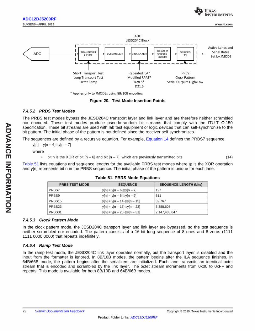
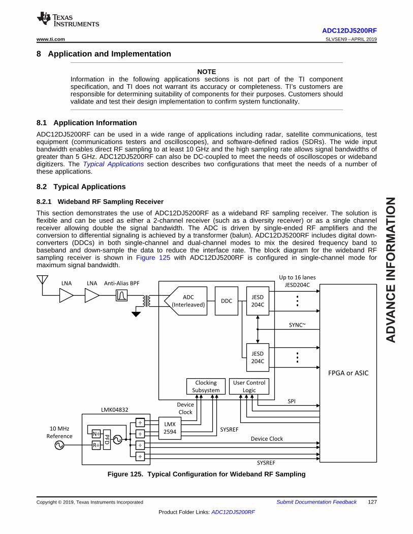
7.1 OverviewADC12DJ5200RF device is an RF-sampling, giga-sample, analog-to-digital converter (ADC) that can directlysample input frequencies from DC to above 10 GHz. In dual-channel mode, the ADC12DJ5200RF can sampleup to 5.2 GSPS and up to 10.4 GSPS in single-channel mode. Programmable tradeoffs in channel count (dual-channel mode) and Nyquist bandwidth (single-channel mode) allow development of flexible hardware that meetsthe needs of both high channel count or wide instantaneous signal bandwidth applications. Full-power inputbandwidth (–3 dB) of 8.0 GHz, with usable frequencies exceeding the –3-dB point in both dual- and single-channel modes, allows direct RF sampling of L-band, S-band, C-band, and X-band for frequency agile systems.
ADC12DJ5200RF uses a high-speed JESD204C output interface with up to 16 serialized lanes and subclass-1compliance for deterministic latency and multi-device synchronization. The serial output lanes support up to17.16 Gbps and can be configured to trade-off bit rate and number of lanes. Both 8B/10B and 64B/66B dataencoding schemes are supported. The 64B/66B encoding schemes support forward error correction (FEC) forimproved bit error rates. The JESD204C interface is backwards compatible with JESD204B receivers when using8B/10B encoding modes.
A number of synchronization features, including noiseless aperture delay (tAD) adjustment and SYSREFwindowing, simplify system design for multi-channel systems. Aperture delay adjustment can be used to simplifySYSREF capture, to align the sampling instance between multiple ADCs or to sample an ideal location of a front-end track and hold (T&H) amplifier output. SYSREF windowing offers a simplistic way to measure invalid timingregions of SYSREF relative to the device clock and then choose an optimal sampling location. Dual-edgesampling (DES) is implemented in single-channel mode to reduce the maximum clock rate applied to the ADC tosupport a wide range of clock sources and relax setup and hold timing for SYSREF capture.
Optional digital down converters (DDCs) are available in both single-channel mode and dual-channel mode toallow a reduction in interface rate (decimation) and digital mixing of the signal to baseband. Single-channel modesupports a single DDC while dual-channel mode supports one DDC per channel. The DDC block supports datadecimation of 4x or 8x and alias-free complex output bandwidths of 80% of the effective output data rate.
ADC12DJ5200RF provides foreground and background calibration options for gain, offset and static linearityerrors. Foreground calibration is run at system startup or at specified times during which the ADC is offline andnot sending data to the logic device. Background calibration allows the ADC to run continually while the coresare calibrated in the background so that the system does not experience downtime. The calibration routine isalso used to match the gain and offset between sub-ADC cores to minimize spurious artifacts from timeinterleaving.
7.3.1 Device ComparisonThe devices listed in Table 1 are part of a pin-to-pin compatible, high-speed, wide-bandwidth ADC family. Thefamily is offered to provide a scalable family of devices for varying resolution, sampling rate and signalbandwidth.
Table 1. Device Family Comparison
PART NUMBER MAXIMUMSAMPLING RATE RESOLUTION DUAL CHANNEL
ADC12DJ3200 Single 6.4 GSPSDual 3.2 GSPS 12-bit Real: 2x
Complex: 4x, 8x, 16x None JESD204B(12.8 Gbps)
ADC08DJ3200 Single 6.4 GSPSDual 3.2 GSPS 8-bit None None JESD204B
(12.8 Gbps)
ADC12DJ2700 Single 5.4 GSPSDual 2.7 GSPS 12-bit Real: 2x
Complex: 4x, 8x, 16x None JESD204B(12.8 Gbps)
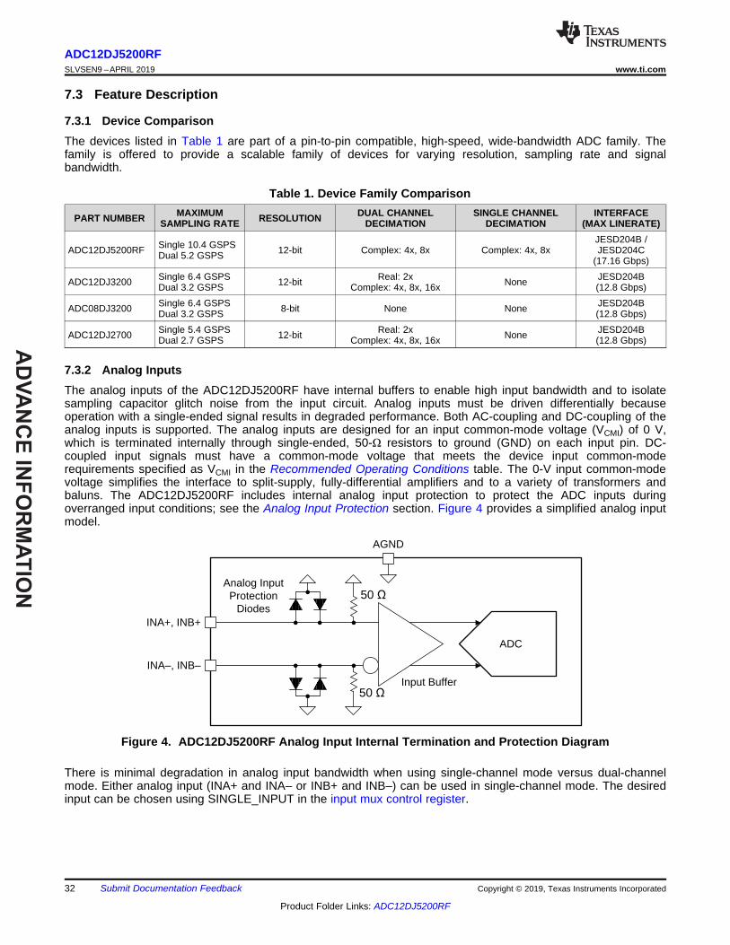
7.3.2 Analog InputsThe analog inputs of the ADC12DJ5200RF have internal buffers to enable high input bandwidth and to isolatesampling capacitor glitch noise from the input circuit. Analog inputs must be driven differentially becauseoperation with a single-ended signal results in degraded performance. Both AC-coupling and DC-coupling of theanalog inputs is supported. The analog inputs are designed for an input common-mode voltage (VCMI) of 0 V,which is terminated internally through single-ended, 50-Ω resistors to ground (GND) on each input pin. DC-coupled input signals must have a common-mode voltage that meets the device input common-moderequirements specified as VCMI in the Recommended Operating Conditions table. The 0-V input common-modevoltage simplifies the interface to split-supply, fully-differential amplifiers and to a variety of transformers andbaluns. The ADC12DJ5200RF includes internal analog input protection to protect the ADC inputs duringoverranged input conditions; see the Analog Input Protection section. Figure 4 provides a simplified analog inputmodel.
Figure 4. ADC12DJ5200RF Analog Input Internal Termination and Protection Diagram
There is minimal degradation in analog input bandwidth when using single-channel mode versus dual-channelmode. Either analog input (INA+ and INA– or INB+ and INB–) can be used in single-channel mode. The desiredinput can be chosen using SINGLE_INPUT in the input mux control register.
7.3.2.1 Analog Input ProtectionThe analog inputs are protected against overdrive conditions by internal clamping diodes that are capable ofsourcing or sinking input currents during overrange conditions, see the voltage and current limits in the AbsoluteMaximum Ratings table. The overrange protection is also defined for a peak RF input power in the AbsoluteMaximum Ratings table, which is frequency independent. Operation above the maximum conditions listed in theRecommended Operating Conditions table results in an increase in failure-in-time (FIT) rate, so the system mustcorrect the overdrive condition as quickly as possible. Figure 4 shows the analog input protection diodes.
7.3.2.2 Full-Scale Voltage (VFS) AdjustmentInput full-scale voltage (VFS) adjustment is available, in fine increments, for each analog input through theFS_RANGE_A register setting (see the INA full-scale range adjust register) and FS_RANGE_B register setting(see the INB full-scale range adjust register) for INA± and INB±, respectively. The available adjustment range isspecified in the Electrical Characteristics: DC Specifications table. Larger full-scale voltages improve SNR andnoise floor (in dBFS/Hz) performance, but can degrade harmonic distortion. The full-scale voltage adjustment isuseful for matching the full-scale range of multiple ADCs when developing a multi-converter system or forexternal interleaving of multiple ADC12DJ5200RFs to achieve higher sampling rates.
7.3.2.3 Analog Input Offset AdjustThe input offset voltage for each input and for each ADC core can be adjusted through SPI registers. TheOADJ_A_FG0_VINx and OADJ_A_FG90_VINx registers (registers 0x344 to 0x34A) are used to adjust ADC coreA's offset voltage when sampling analog input x (where x is A for INA± or B for INB±) where the FG0 register isused for dual channel mode and FG90 is used for single channel mode. OADJ_B_FG0_VINx is used to adjustADC core B's offset voltage when sampling input x. OADJ_B_FG0_VINx applies to both single channel modeand dual channel mode. To adjust the offset voltage in dual channel mode simply adjust the offset for the ADCcore sampling the desired input. In single channel mode, both ADC core A's offset and ADC core B's offset mustbe adjusted together. The difference in the two core's offsets in single channel mode will result in a spur at fS/2that is independent of the input. These registers can be used to compensate the fS/2 spur in single channelmode. See the Calibration Modes and Trimming section for more information.
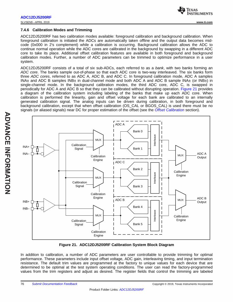
7.3.3 ADC CoreThe ADC12DJ5200RF consists of a total of six ADC cores. The cores are interleaved for higher sampling ratesand swapped on-the-fly for calibration as required by the operating mode. This section highlights the theory andkey features of the ADC cores.
7.3.3.1 ADC Theory of OperationThe differential voltages at the analog inputs are captured by the rising edge of CLK± in dual-channel mode or bythe rising and falling edges of CLK± in single-channel mode. After capturing the input signal, the ADC convertsthe analog voltage to a digital value by comparing the voltage to the internal reference voltage. If the voltage onINA– or INB– is higher than the voltage on INA+ or INB+, respectively, then the digital output is a negative 2'scomplement value. If the voltage on INA+ or INB+ is higher than the voltage on INA– or INB–, respectively, thenthe digital output is a positive 2's complement value. Equation 1 can calculate the differential voltage at the inputpins from the digital output.
where• Code is the signed decimation output code (for example, –2048 to +2047)• N is the ADC resolution• and VFS is the full-scale input voltage of the ADC as specified in the Recommended Operating Conditions
table, including any adjustment performed by programming FS_RANGE_A or FS_RANGE_B (1)
7.3.3.2 ADC Core CalibrationADC core calibration is required to optimize the analog performance of the ADC cores. Calibration must berepeated when operating conditions change significantly, namely temperature, in order to maintain optimalperformance. The ADC12DJ5200RF has a built-in calibration routine that can be run as a foreground operationor a background operation. Foreground operation requires ADC downtime, where the ADC is no longer samplingthe input signal, to complete the process. Background calibration can be used to overcome this limitation andallow constant operation of the ADC. See the Calibration Modes and Trimming section for detailed information oneach mode.
7.3.3.3 Analog Reference VoltageThe reference voltage for the ADC12DJ5200RF is derived from an internal band-gap reference. A bufferedversion of the reference voltage is available at the BG pin for user convenience. This output has an output-current capability of ±100 µA. The BG output must be buffered if more current is required. No provision exists forthe use of an external reference voltage, but the full-scale input voltage can be adjusted through the full-scale-range register settings.
7.3.3.4 ADC Overrange DetectionTo ensure that system gain management has the quickest possible response time, a low-latency configurableoverrange function is included. The overrange function works by monitoring the converted 12-bit samples at theADC to quickly detect if the ADC is near saturation or already in an overrange condition. The absolute value ofthe upper 8 bits of the ADC data are checked against two programmable thresholds, OVR_T0 and OVR_T1.These thresholds apply to both channel A and channel B in dual-channel mode. Table 2 lists how an ADCsample is converted to an absolute value for a comparison of the thresholds.
Table 2. Conversion of ADC Sample for Overrange ComparisonADC SAMPLE(Offset Binary)
ADC SAMPLE(2's Complement) ABSOLUTE VALUE UPPER 8 BITS USED FOR
If the upper 8 bits of the absolute value equal or exceed the OVR_T0 or OVR_T1 thresholds during themonitoring period, then the overrange bit associated with the threshold is set to 1, otherwise the overrange bit is0. In dual-channel mode, the overrange status can be monitored on the ORA0 and ORA1 pins for channel A andthe ORB0 and ORB1 pins for channel B, where ORx0 corresponds to the OVR_T0 threshold and ORx1corresponds to the OVR_T1 threshold. In single-channel mode, the overrange status for the OVR_T0 thresholdis determined by monitoring both the ORA0 and ORB0 outputs and the OVR_T1 threshold is determined bymonitoring both ORA1 and ORB1 outputs. In single-channel mode, the two outputs for each threshold must beOR'd together to determine whether an overrange condition occurred. OVR_N can be used to set the outputpulse duration from the last overrange event. Table 3 lists the overrange pulse lengths for the various OVR_Nsettings (see the overrange configuration register). In decimation modes (only in the JMODEs where CS = 1 inTable 22), the overrange status is also embedded into the output data samples where the OVR_T0 thresholdstatus is embedded as the LSB along with the upper 15 bits of every complex I sample and the OVR_T1threshold status is embedded as the LSB along with the upper 15 bits of every complex Q sample. Table 4 liststhe outputs, related data samples, threshold settings, and the monitoring period equation. The embeddedoverrange bit goes high if the associated channel exceeds the associated overrange threshold within themonitoring period set by OVR_N. Use Table 4 to calculate the monitoring period.
Table 3. Overrange Monitoring Period for the ORA0, ORA1, ORB0, and ORB1 Outputs
OVR_N OVERRANGE PULSE LENGTH SINCE LAST OVERRANGEEVENT (DEVCLK Cycles)
0 81 162 323 644 1285 2566 5127 1024
(1) OVR_N is the monitoring period register setting.
Table 4. Threshold and Monitoring Period for Embedded Overrange Indicators in Dual-ChannelDecimation Modes
OVERRANGEINDICATOR
ASSOCIATEDTHRESHOLD DECIMATION TYPE OVERRANGE STATUS
EMBEDDED INMONITORING PERIOD
(ADC Samples)
ORA0 OVR_T0 Complex down-conversion Channel A in-phase (I)samples 2OVR_N(1)
ORA1 OVR_T1 Complex down-conversion Channel A quadrature(Q) samples 2OVR_N(1)
ORB0 OVR_T0 Complex down-conversion Channel B in-phase (I)samples 2OVR_N(1)
ORB1 OVR_T1 Complex down-conversion Channel B quadrature(Q) samples 2OVR_N(1)
Typically, the OVR_T0 threshold can be set near the full-scale value (228 for example). When the threshold istriggered, a typical system can turn down the system gain to avoid clipping. The OVR_T1 threshold can be setmuch lower. For example, the OVR_T1 threshold can be set to 64 (peak input voltage of −12 dBFS). If the inputsignal is strong, the OVR_T1 threshold is tripped occasionally. If the input is quite weak, the threshold is nevertripped. The downstream logic device monitors the OVR_T1 bit. If OVR_T1 stays low for an extended period oftime, then the system gain can be increased until the threshold is occasionally tripped (meaning the peak level ofthe signal is above −12 dBFS).
7.3.3.5 Code Error Rate (CER)ADC cores can generate bit errors within a sample, often called code errors (CER) or referred to as sparklecodes, resulting from metastability caused by non-ideal comparator limitations. The ADC12DJ5200RF uses aunique ADC architecture that inherently allows significant code error rate improvements from traditional pipelinedflash or successive approximation register (SAR) ADCs. The code error rate of the ADC12DJ5200RF is multipleorders of magnitude better than what can be achieved in alternative architectures at equivalent sampling ratesproviding significant signal reliability improvements.
7.3.4 Temperature Monitoring DiodeA built-in thermal monitoring diode is made available on the TDIODE+ and TDIODE– pins. This diode facilitatestemperature monitoring and characterization of the device in higher ambient temperature environments. Althoughthe on-chip diode is not highly characterized, the diode can be used effectively by performing a baselinemeasurement (offset) at a known ambient or board temperature and creating a linear equation with the diodevoltage slope provided in the Electrical Characteristics: DC Specifications table. Perform offset measurementwith the device unpowered or with the PD pin asserted to minimize device self-heating. Recommendedmonitoring devices include the LM95233 device and similar remote-diode temperature monitoring products fromTexas Instruments.
7.3.5 TimestampThe TMSTP+ and TMSTP– differential input can be used as a time-stamp input to mark a specific sample basedon the timing of an external trigger event relative to the sampled signal. TIMESTAMP_EN (see the LSB controlbit output register) must be set in order to use the timestamp feature and output the timestamp data. Whenenabled, the LSB of the 12-bit ADC digital output reports the status of the TMSTP± input. In effect, the 12-bitoutput sample consists of the upper 11-bits of the 12-bit converter and the LSB of the 12-bit output sample is theoutput of a parallel 1-bit converter (TMSTP±) with the same latency as the ADC core. In the 8-bit operatingmodes, the LSB of the 8-bit output sample is used to output the timestamp status. The trigger must be applied tothe differential TMSTP+ and TMSTP– inputs. The trigger can be asynchronous to the ADC sampling clock and issampled at approximately the same time as the analog input. Timestamp cannot be used when a JMODE withdecimation is selected and instead SYSREF must be used to achieve synchronization through the JESD204Csubclass-1 method for achieving deterministic latency.
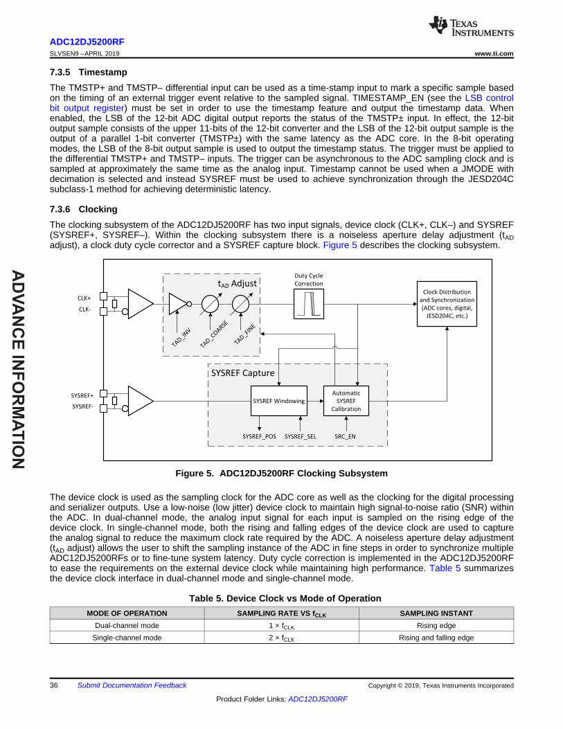
7.3.6 ClockingThe clocking subsystem of the ADC12DJ5200RF has two input signals, device clock (CLK+, CLK–) and SYSREF(SYSREF+, SYSREF–). Within the clocking subsystem there is a noiseless aperture delay adjustment (tADadjust), a clock duty cycle corrector and a SYSREF capture block. Figure 5 describes the clocking subsystem.
Figure 5. ADC12DJ5200RF Clocking Subsystem
The device clock is used as the sampling clock for the ADC core as well as the clocking for the digital processingand serializer outputs. Use a low-noise (low jitter) device clock to maintain high signal-to-noise ratio (SNR) withinthe ADC. In dual-channel mode, the analog input signal for each input is sampled on the rising edge of thedevice clock. In single-channel mode, both the rising and falling edges of the device clock are used to capturethe analog signal to reduce the maximum clock rate required by the ADC. A noiseless aperture delay adjustment(tAD adjust) allows the user to shift the sampling instance of the ADC in fine steps in order to synchronize multipleADC12DJ5200RFs or to fine-tune system latency. Duty cycle correction is implemented in the ADC12DJ5200RFto ease the requirements on the external device clock while maintaining high performance. Table 5 summarizesthe device clock interface in dual-channel mode and single-channel mode.
Table 5. Device Clock vs Mode of OperationMODE OF OPERATION SAMPLING RATE VS fCLK SAMPLING INSTANT
SYSREF is a system timing reference used for JESD204C subclass-1 implementations of deterministic latency.SYSREF is used to achieve deterministic latency and for multi-device synchronization. SYSREF must becaptured by the correct device clock edge in order to achieve repeatable latency and synchronization. TheADC12DJ5200RF includes SYSREF windowing and automatic SYSREF calibration to ease the requirements onthe external clocking circuits and to simplify the synchronization process. SYSREF can be implemented as asingle pulse or as a periodic clock. In periodic implementations, SYSREF must be equal to, or an integer divisionof, the local multiframe clock frequency in 8B/10B encoding modes or the local extended multiblock clockfrequency in 64B/66B encoding modes. Equation 2 is used to calculate valid SYSREF frequencies in 8B/10Bencoding modes. In 64B/66B modes, the denominator changes to 66 × 32 × E × n, where E is the number ofmultiblocks in an extended multiblock.
where• R and F are set by the JMODE setting (see Table 22)• fCLK is the device clock frequency (CLK±)• K is the programmed multiframe length (see Table 22 for valid K settings)• and n is any positive integer (2)
7.3.6.1 Noiseless Aperture Delay Adjustment (tAD Adjust)The ADC12DJ5200RF contains a delay adjustment on the device clock (sampling clock) input path, called tADadjust, that can be used to shift the sampling instance within the device in order to align sampling instancesamong multiple devices or for external interleaving of multiple ADC12DJ5200RFs. Further, tAD adjust can beused for automatic SYSREF calibration to simplify synchronization; see the Automatic SYSREF Calibrationsection. Aperture delay adjustment is implemented in a way that adds no additional noise to the clock path,however a slight degradation in aperture jitter (tAJ) is possible at large values of TAD_COARSE because ofinternal clock path attenuation. The degradation in aperture jitter can result in minor SNR degradations at highinput frequencies (see tAJ in the Switching Characteristics table). This feature is programmed using TAD_INV,TAD_COARSE, and TAD_FINE in the DEVCLK timing adjust ramp control register. Setting TAD_INV inverts theinput clock resulting in a delay equal to half the clock period. Table 6 summarizes the step sizes and ranges ofthe TAD_COARSE and TAD_FINE variable analog delays. All three delay options are independent and can beused in conjunction. All clocks within the device are shifted by the programmed tAD adjust amount, which resultsin a shift of the timing of the JESD204C serialized outputs and affects the capture of SYSREF.
Table 6. tAD Adjust Adjustment RangesADJUSTMENT PARAMETER ADJUSTMENT STEP DELAY SETTINGS MAXIMUM DELAY
TAD_INV 1 / (fCLK × 2) 1 1 / (fCLK × 2)
TAD_COARSE See tTAD(STEP) in the SwitchingCharacteristics table 256 See tTAD(MAX) in the Switching
Characteristics table
TAD_FINE See tTAD(STEP) in the SwitchingCharacteristics table 256 See tTAD(MAX) in the Switching
Characteristics table
In order to maintain timing alignment between converters, stable and matched power-supply voltages and devicetemperatures must be provided.
Aperture delay adjustment can be changed on-the-fly during normal operation but may result in brief upsets tothe JESD204C data link. Use TAD_RAMP to reduce the probability of the JESD204C link losing synchronization;see the Aperture Delay Ramp Control (TAD_RAMP) section.
7.3.6.2 Aperture Delay Ramp Control (TAD_RAMP)The ADC12DJ5200RF contains a function to gradually adjust the tAD adjust setting towards the newly writtenTAD_COARSE value. This functionality allows the tAD adjust setting to be adjusted with minimal internal clockcircuitry glitches. The TAD_RAMP_RATE parameter allows either a slower (one TAD_COARSE LSB per 256tCLK cycles) or faster ramp (four TAD_COARSE LSBs per 256 tCLK cycles) to be selected. The TAD_RAMP_ENparameter enables the ramp feature and any subsequent writes to TAD_COARSE initiate a new cramp.
7.3.6.3 SYSREF Capture for Multi-Device Synchronization and Deterministic LatencyThe clocking subsystem is largely responsible for achieving multi-device synchronization and deterministiclatency. The ADC12DJ5200RF uses the JESD204C subclass-1 method to achieve deterministic latency andsynchronization. Subclass 1 requires that the SYSREF signal be captured by a deterministic device clock (CLK±)edge at each system power-on and at each device in the system. This requirement imposes setup and holdconstraints on SYSREF relative to CLK±, which can be difficult to meet at giga-sample clock rates over allsystem operating conditions. The ADC12DJ5200RF includes a number of features to simplify thissynchronization process and to relax system timing constraints:• The ADC12DJ5200RF uses dual-edge sampling (DES) in single-channel mode to reduce the CLK± input
frequency by half and double the timing window for SYSREF (see Table 5)• A SYSREF position detector (relative to CLK±) and selectable SYSREF sampling position aid the user in
meeting setup and hold times over all conditions; see the SYSREF Position Detector and Sampling PositionSelection (SYSREF Windowing) section
• Easy-to-use automatic SYSREF calibration uses the aperture timing adjust block (tAD adjust) to shift the ADCsampling instance based on the phase of SYSREF (rather than adjusting SYSREF based on the phase of theADC sampling instance); see the Automatic SYSREF Calibration section
7.3.6.3.1 SYSREF Position Detector and Sampling Position Selection (SYSREF Windowing)
The SYSREF windowing block is used to first detect the position of SYSREF relative to the CLK± rising edge andthen to select a desired SYSREF sampling instance, which is a delay version of CLK±, to maximize setup andhold timing margins. In many cases a single SYSREF sampling position (SYSREF_SEL) is sufficient to meettiming for all systems (device-to-device variation) and conditions (temperature and voltage variations). However,this feature can also be used by the system to expand the timing window by tracking the movement of SYSREFas operating conditions change or to remove system-to-system variation at production test by finding a uniqueoptimal value at nominal conditions for each system.
This section describes proper usage of the SYSREF windowing block. First, apply the device clock and SYSREFto the device. The location of SYSREF relative to the device clock cycle is determined and stored in theSYSREF_POS bits of the SYSREF capture position register. ADC12DJ5200RF must see at least 3 rising edgesof SYSREF before the SYSREF_POS output is valid. Each bit of SYSREF_POS represents a potential SYSREFsampling position. If a bit in SYSREF_POS is set to 1, then the corresponding SYSREF sampling position has apotential setup or hold violation. Upon determining the valid SYSREF sampling positions (the positions ofSYSREF_POS that are set to 0) the desired sampling position can be chosen by setting SYSREF_SEL in theclock control register 0 to the value corresponding to that SYSREF_POS position. In general, the middlesampling position between two setup and hold instances is chosen. Ideally, SYSREF_POS and SYSREF_SELare performed at the nominal operating conditions of the system (temperature and supply voltage) to providemaximum margin for operating condition variations. This process can be performed at final test and the optimalSYSREF_SEL setting can be stored for use at every system power up. Further, SYSREF_POS can be used tocharacterize the skew between CLK± and SYSREF± over operating conditions for a system by sweeping thesystem temperature and supply voltages. For systems that have large variations in CLK± to SYSREF± skew, thischaracterization can be used to track the optimal SYSREF sampling position as system operating conditionschange. In general, a single value can be found that meets timing over all conditions for well-matched systems,such as those where CLK± and SYSREF± come from a single clocking device.
NOTESYSREF_SEL must be set to 0 when using automatic SYSREF calibration; see theAutomatic SYSREF Calibration section.
The step size between each SYSREF_POS sampling position can be adjusted using SYSREF_ZOOM. WhenSYSREF_ZOOM is set to 0, the delay steps are coarser. When SYSREF_ZOOM is set to 1, the delay steps arefiner. See the Switching Characteristics table for delay step sizes when SYSREF_ZOOM is enabled anddisabled. In general, SYSREF_ZOOM is recommended to always be used (SYSREF_ZOOM = 1) unless atransition region (defined by 1's in SYSREF_POS) is not observed, which can be the case for low clock rates.Bits 0 and 23 of SYSREF_POS are always be set to 1 because there is insufficient information to determine ifthese settings are close to a timing violation, although the actual valid window can extend beyond these samplingpositions. The value programmed into SYSREF_SEL is the decimal number representing the desired bit locationin SYSREF_POS. Table 7 lists some example SYSREF_POS readings and the optimal SYSREF_SEL settings.
(1) Red coloration indicates the bits that are selected, as given in the last column of this table.
Although 24 sampling positions are provided by the SYSREF_POS status register, SYSREF_SEL only allowsselection of the first 16 sampling positions, corresponding to SYSREF_POS bits 0 to 15. The additionalSYSREF_POS status bits are intended only to provide additional knowledge of the SYSREF valid window. Ingeneral, lower values of SYSREF_SEL are selected because of delay variation over supply voltage, however inthe fourth example a value of 15 provides additional margin and can be selected instead.
Table 7. Examples of SYSREF_POS Readings and SYSREF_SEL SelectionsSYSREF_POS[23:0]
OPTIMAL SYSREF_SELSETTING0x02E[7:0]
(Largest Delay) 0x02D[7:0] (1) 0x02C[7:0] (1)
(Smallest Delay)b10000000 b01100000 b00011001 8 or 9b10011000 b00000000 b00110001 12b10000000 b01100000 b00000001 6 or 7b10000000 b00000011 b00000001 4 or 15b10001100 b01100011 b00011001 6
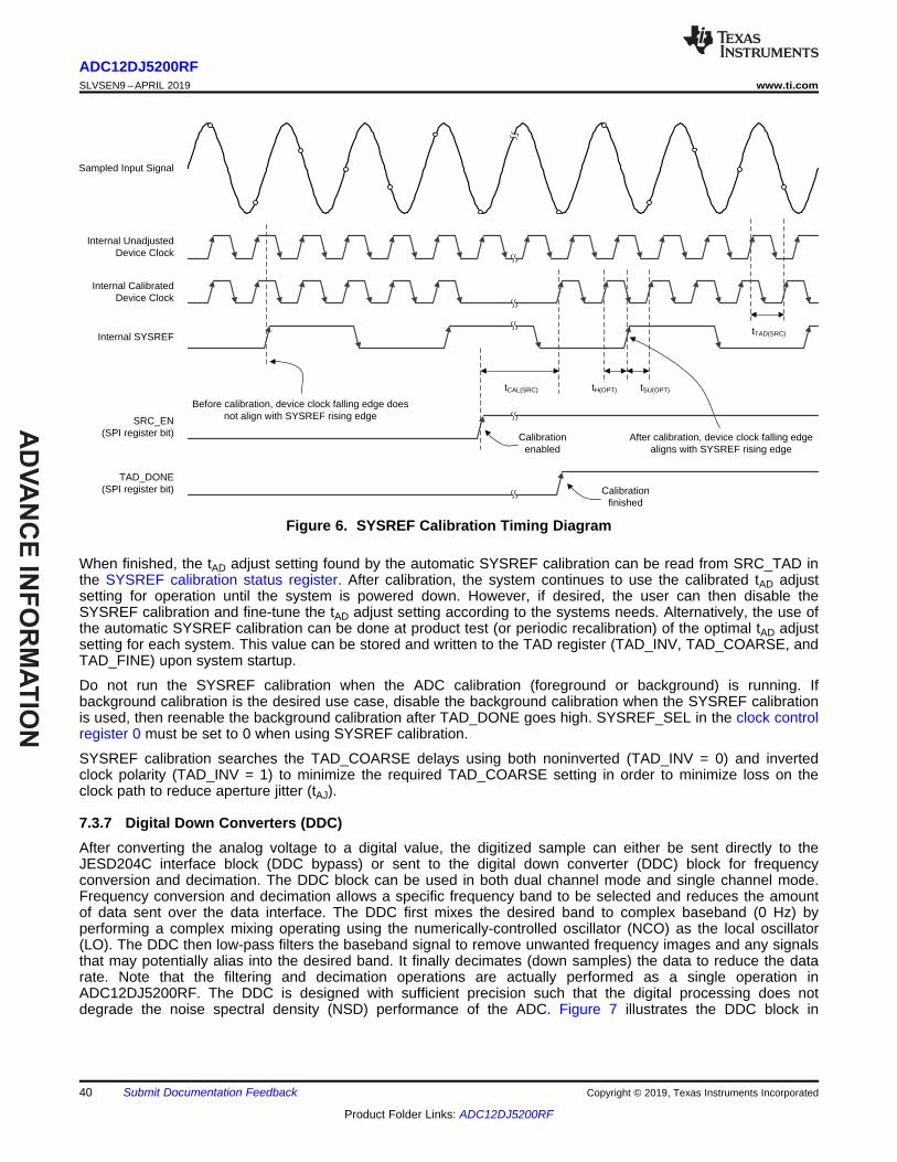
7.3.6.3.2 Automatic SYSREF Calibration
The ADC12DJ5200RF has an automatic SYSREF calibration feature to alleviate the often challenging setup andhold times associated with capturing SYSREF for giga-sample data converters. Automatic SYSREF calibrationuses the tAD adjust feature to shift the device clock to maximize the SYSREF setup and hold times or to align thesampling instance based on the SYSREF rising edge.
The ADC12DJ5200RF must have a proper device clock applied and be programmed for normal operation beforestarting the automatic SYSREF calibration. When ready to initiate automatic SYSREF calibration, a continuousSYSREF signal must be applied. SYSREF must be a continuous (periodic) signal when using the automaticSYSREF calibration. Start the calibration process by setting SRC_EN high in the SYSREF calibration enableregister after configuring the automatic SYSREF calibration using the SRC_CFG register. Upon setting SRC_ENhigh, the ADC12DJ5200RF searches for the optimal tAD adjust setting until the device clock falling edge isinternally aligned to the SYSREF rising edge. TAD_DONE in the SYSREF calibration status register can bemonitored to ensure that the SYSREF calibration has finished. By aligning the device clock falling edge with theSYSREF rising edge, automatic SYSREF calibration maximizes the internal SYSREF setup and hold timesrelative to the device clock and also sets the sampling instant based on the SYSREF rising edge. After theautomatic SYSREF calibration finishes, the rest of the startup procedure can be performed to finish bringing upthe system.
For multi-device synchronization, the SYSREF rising edge timing must be matched at all devices and thereforetrace lengths must be matched from a common SYSREF source to each ADC12DJ5200RF. Any skew betweenthe SYSREF rising edge at each device results in additional error in the sampling instance between devices,however repeatable deterministic latency from system startup to startup through each device must still beachieved. No other design requirements are needed in order to achieve multi-device synchronization as long asa proper elastic buffer release point is chosen in the JESD2048 receiver.
Figure 6 provides a timing diagram of the SYSREF calibration procedure. The optimized setup and hold timesare shown as tSU(OPT) and tH(OPT), respectively. Device clock and SYSREF are referred to as internal in thisdiagram because the phase of the internal signals are aligned within the device and not to the external (applied)phase of the device clock or SYSREF.
When finished, the tAD adjust setting found by the automatic SYSREF calibration can be read from SRC_TAD inthe SYSREF calibration status register. After calibration, the system continues to use the calibrated tAD adjustsetting for operation until the system is powered down. However, if desired, the user can then disable theSYSREF calibration and fine-tune the tAD adjust setting according to the systems needs. Alternatively, the use ofthe automatic SYSREF calibration can be done at product test (or periodic recalibration) of the optimal tAD adjustsetting for each system. This value can be stored and written to the TAD register (TAD_INV, TAD_COARSE, andTAD_FINE) upon system startup.
Do not run the SYSREF calibration when the ADC calibration (foreground or background) is running. Ifbackground calibration is the desired use case, disable the background calibration when the SYSREF calibrationis used, then reenable the background calibration after TAD_DONE goes high. SYSREF_SEL in the clock controlregister 0 must be set to 0 when using SYSREF calibration.
SYSREF calibration searches the TAD_COARSE delays using both noninverted (TAD_INV = 0) and invertedclock polarity (TAD_INV = 1) to minimize the required TAD_COARSE setting in order to minimize loss on theclock path to reduce aperture jitter (tAJ).
7.3.7 Digital Down Converters (DDC)After converting the analog voltage to a digital value, the digitized sample can either be sent directly to theJESD204C interface block (DDC bypass) or sent to the digital down converter (DDC) block for frequencyconversion and decimation. The DDC block can be used in both dual channel mode and single channel mode.Frequency conversion and decimation allows a specific frequency band to be selected and reduces the amountof data sent over the data interface. The DDC first mixes the desired band to complex baseband (0 Hz) byperforming a complex mixing operating using the numerically-controlled oscillator (NCO) as the local oscillator(LO). The DDC then low-pass filters the baseband signal to remove unwanted frequency images and any signalsthat may potentially alias into the desired band. It finally decimates (down samples) the data to reduce the datarate. Note that the filtering and decimation operations are actually performed as a single operation inADC12DJ5200RF. The DDC is designed with sufficient precision such that the digital processing does notdegrade the noise spectral density (NSD) performance of the ADC. Figure 7 illustrates the DDC block in
ADC12DJ5200RF in dual channel mode while Figure 8 shows the DDC block of ADC12DJ5200RF in singlechannel mode. In dual channel mode, the input data for each DDC can be selected to come from either ADCchannel A or ADC channel B by using the DIG_BIND_x SPI registers. Channel B has the same structure with theinput data selected by DIG_BIND_B and the NCO selection mux controlled by pins NCOB[1:0] or throughCSELB[1:0]. Only one DDC is available for use in single channel mode.
Figure 7. Digital Down Conversion Block in Dual Channel Mode
Figure 8. Digital Down Conversion Block in Single Channel Mode
7.3.7.1 Numerically-Controlled Oscillator and Complex MixerThe DDC contains a complex numerically-controlled oscillator (NCO) and a complex mixer. Equation 3 shows thecomplex exponential sequence generated by the oscillator.
x[n] = ejωn (3)
The frequency (ω) is specified by a 32-bit register setting (see the Basic NCO Frequency Setting Mode sectionand the Rational NCO Frequency Setting Mode section). The complex exponential sequence is multiplied by thereal input from the ADC to mix the desired carrier to a frequency equal to fIN + fNCO, where fIN is the analog inputfrequency after aliasing (in undersampling systems) and fNCO is the programmed NCO frequency.
7.3.7.1.1 NCO Fast Frequency Hopping (FFH)
Fast frequency hopping (FFH) is made possible by each DDC having four independent NCOs that can becontrolled by the NCOA0 and NCOA1 pins for DDC A and the NCOB0 and NCOB1 pins for DDC B. Each NCOhas independent frequency settings (see the Basic NCO Frequency Setting Mode section) and initial phasesettings (see the NCO Phase Offset Setting section) that can be set independently. Further, all NCOs haveindependent phase accumulators that continue to run when the specific NCO is not selected, allowing the NCOsto maintain their phase between selection so that downstream processing does not need to perform carrierrecovery after each hop, for instance.
NCO hopping occurs when the NCO GPIO pins change state. The pins are controlled asynchronously andtherefore synchronous switching is not possible. Associated latencies are demonstrated in Figure 9, where tTXand tADC are provided in the Switching Characteristics table. All latencies in Table 8 are approximations only.
Figure 9. NCO Fast Frequency Hopping Latency Diagram
Table 8. NCO Fast Frequency Hopping Latency DefinitionsLATENCY PARAMETER VALUE OR CALCULATION UNITS
Within each channel DDC, four different frequency and phase settings are available for use. Each of the foursettings use a different phase accumulator within the NCO. Because all four phase accumulators areindependent and continuously running, rapid switching between different NCO frequencies is possible allowingfor phase coherent frequency hopping.
The specific frequency-phase pair used for each channel is selected through the NCOA[1:0] or NCOB[1:0] inputpins when CMODE is set to 1. Alternatively, the selected NCO can be chosen through SPI by CSELA for DDC Aand CSELB for DDC B by setting CMODE to 0 (default). The logic table for NCO selection is provided in Table 9for both the GPIO and SPI selection options.
Table 9. Logic Table for NCO Selection Using GPIO or SPINCO SELECTION CMODE NCOx1 NCOx0 CSELx[1] CSELx[0]NCO 0 using GPIO 1 0 0 X XNCO 1 using GPIO 1 0 1 X XNCO 2 using GPIO 1 1 0 X XNCO 3 using GPIO 1 1 1 X XNCO 0 using SPI 0 X X 0 0NCO 1 using SPI 0 X X 0 1NCO 2 using SPI 0 X X 1 0NCO 3 using SPI 0 X X 1 1
The frequency for each phase accumulator is programmed independently through the FREQAx, FREQBx (x = 0to 3) and, optionally, NCO_RDIV register settings. The phase offset for each accumulator is programmedindependently through the PHASEAx and PHASEBx (x = 0 to 3) register settings.
7.3.7.1.3 Basic NCO Frequency Setting Mode
In basic NCO frequency-setting mode (NCO_RDIV = 0x0000), the NCO frequency setting is set by the 32-bitregister value, FREQAx and FREQBx (x = 0 to 3). The NCO frequency for DDC A can be calculated usingEquation 4, where FREQAx can be replaced by FREQBx to calculate the NCO frequency for DDC B. FREQAxand FREQBx can be considered either a 2's complement number (–2147483648 to 2147483647) or as an offsetbinary number (0 to 4294967295).
NOTEChanging the FREQAx and FREQBx register settings during operation results in a non-deterministic NCO phase. If deterministic phase is required, the NCOs must beresynchronized; see the NCO Phase Synchronization section.
7.3.7.1.4 Rational NCO Frequency Setting Mode
In basic NCO frequency mode, the frequency step size is very small and many frequencies can be synthesized,but sometimes an application requires very specific frequencies that fall between two frequency steps. Forexample with ƒS equal to 2457.6 MHz and a desired ƒ(NCO) equal to 5.02 MHz, the value for FREQAx is8773085.867. Truncating the fractional portion results in an ƒ(NCO) equal to 5.0199995 MHz, which is not thedesired frequency.
To produce the desired frequency, the NCO_RDIV parameter is used to force the phase accumulator to arrive atspecific frequencies without error. First, select a frequency step size (ƒ(STEP)) that is appropriate for the NCOfrequency steps required. The typical value of ƒ(STEP) is 10 kHz. Next, use Equation 5 to program the NCO_RDIVvalue.
(5)
The result of Equation 5 must be an integer value. If the value is not an integer, adjust either of the parametersuntil the result is an integer value.
For example, select a value of 1920 for NCO_RDIV.
NOTENCO_RDIV values larger than 8192 can degrade the NCO SFDR performance and arenot recommended.
Now use Equation 6 to calculate the FREQAx register value.
(6)
Alternatively, the following equations can be used:
Table 10 lists common values for NCO_RDIV in 10-kHz frequency steps.
Table 10. Common NCO_RDIV Values (For 10-kHz Frequency Steps)fCLK (MHz) NCO_RDIV
2457.6 38401966.08 3072
1600 25001474.56 23041228.8 1920
7.3.7.1.5 NCO Phase Offset Setting
The NCO phase-offset setting for each NCO is set by the 16-bit register value PHASEAx and PHASEBx (wherex = 0 to 3). The value is left-justified into a 32-bit field and then added to the phase accumulator.
Use Equation 9 to calculate the phase offset in radians.Φ(rad) = PHASEA/Bx × 2–16 × 2 × π (x = 0 to 3) (9)
7.3.7.1.6 NCO Phase Synchronization
The NCOs must be synchronized after setting or changing the value of FREQAx or FREQBx. NCOsynchronization is performed when the JESD204C link is initialized or by SYSREF, based on the settings ofNCO_SYNC_ILA and NCO_SYNC_NEXT. The procedures are as follows for the JESD204C initializationprocedure and the SYSREF procedure for both DC-coupled and AC-coupled SYSREF signals.
NCO synchronization using the JESD204C SYNC signal (SYNCSE or TMSTP±). Although the 64B/66B encodingmodes do not use the SYNC signal to initialize the JESD204C link, it can still be used for NCO synchronizationwith this method:1. The device must be programmed for normal operation2. Set NCO_SYNC_ILA to 1 to enable NCO synchronization using the SYNC signal3. Set JESD_EN to 04. Program FREQAx, FREQBx, PHASEAx, and PHASEBx to the desired settings5. In the JESD204C receiver (logic device), deassert the SYNC signal by setting SYNC high6. Set JESD_EN to 17. Assert the SYNC signal by setting SYNC low in the JESD204C receiver. This start the code group
synchronization (CGS) process in 8B/10B encoding modes or arms the trigger in 64B/66B encoding modes.8. After achieving CGS (or when ready to synchronize), deassert the SYNC signal by setting SYNC high at the
same time for all ADCs in order synchronize the NCOs in each ADC. The SYNC signal must meet therequired setup and hold times (as specified in the Timing Requirements table)
NCO synchronization using SYSREF (DC-coupled):1. The device must be programmed for normal operation2. Set JESD_EN to 1 to start the JESD204C link (the SYNC signal can respond as normal during the CGS
process)3. Program FREQAx, FREQBx, PHASEAx, and PHASEBx to the desired settings4. Verify that SYSREF is disabled (held low)5. Arm NCO synchronization by setting NCO_SYNC_NEXT to 16. Issue a single SYSREF pulse to all ADCs to synchronize NCOs within all devices
NCO synchronization using SYSREF (AC-coupled):1. The device must be programmed for normal operation2. Set JESD_EN to 1 to start the JESD204C link (the SYNC signal can respond as normal during the CGS
process)3. Program FREQAx, FREQBx, PHASEAx, and PHASEBx to the desired settings4. Run SYSREF continuously5. Arm NCO synchronization by setting NCO_SYNC_NEXT to 1 at the same time at all ADCs by timing the
rising edge of SCLK for the last data bit (LSB) at the end of the SPI write so that the SCLK rising edgeoccurs after a SYSREF rising edge and early enough before the next SYSREF rising edge so that the triggeris armed before the next SYSREF rising edge (a long SYSREF period is recommended)
6. NCOs in all ADCs are synchronized by the next SYSREF rising edge
7.3.7.2 Decimation FiltersThe decimation filters are arranged to provide a programmable overall decimation of 4 or 8. All decimation filtersoperate on complex data (from the complex digital mixer) and the outputs have a resolution of 15 bits. Thedecimation filters are implemented as linear phase finite impulse response (FIR) filters. Table 11 lists theeffective output sample rates, available signal bandwidths, output formats, and stop-band attenuation for eachdecimation mode.
Table 11. Output Sample Rates and Signal Bandwidths
DECIMATIONSETTING
ƒ(DEVCLK)OUTPUT FORMATOUTPUT RATE
(MSPS)MAX ALIAS PROTECTED SIGNAL
BANDWIDTH (MHz)STOP-BAND
ATTENUATIONPASS-BAND
RIPPLENo decimation (DDC
bypass) ƒ(DEVCLK) ƒ(DEVCLK) / 2 — < ±0.001 dB Real signal,12-bit data
Decimate-by-4 ƒ(DEVCLK) / 4 0.8 × ƒ(DEVCLK) / 4 > 90 dB < ±0.001 dB Complex signal,15-bit data
Decimate-by-8 ƒ(DEVCLK) / 8 0.8 × ƒ(DEVCLK) / 8 > 90 dB < ±0.001 dB Complex signal,15-bit data
Figure 10 to Figure 13 provide the composite decimation filter responses. The black portion of the trace showsthe pass-band region, or alias-protected region, of the response. The red portion of the trace shows the transitionregion of the response as well as any frequency regions that will alias into the transition region. The transitionregion is not alias protected and therefore desired signals should only be placed in the pass-band region of thefilter response. The blue portion of the trace shows the frequency regions that will alias into the pass-band afterdecimation and therefore define the stop-band region of the frequency response. The stop-band attenuation isdefined to sufficient filter any undesired images or signals to prevent them from aliasing into the desired pass-band. Use analog filtering before the analog inputs (INA± or INB±) for additional attenuation of signals that fallwithin this band or to sufficiently reduce signals at the ADC inputs that may produce harmonics, interleavingspurs or other undesired spurious signals that will alias into the desired signal band (before the complex mixingand decimation operations).
For maximum efficiency, a group of high-speed filter blocks are implemented with specific blocks used for eachdecimation setting to achieve the composite responses illustrated in Figure 10 to Figure 13. Table 12 describesthe combination of filter blocks used for each decimation setting and Table 13 lists the coefficient details anddecimation factor of each filter block. The coefficients are symmetric with the center tap indicated by bold text.
Table 12. Decimation Mode Filter UsageDECIMATION SETTING FILTER BLOCKS USED (Listed in Order of Operation)
Table 13. Filter Coefficient DetailsFILTER COEFFICIENT SET (Decimation Factor of Filter, Scale factor)
CS20 (2, 2-14) CS40 (2, 2-17) CS80 (2, 2-19)
109 109 –327 –327 –37 –37
0 0 0 0 0 0
–837 –837 2231 2231 118 118
0 0 0 0 0 0
4824 4824 –8881 –8881 –291 –291
8192 0 0 0 0
39742 39742 612 612
65536 0 0
–1159 –1159
0 0
2031 2031
0 0
–3356 –3356
0 0
5308 5308
0 0
–8140 –8140
0 0
12284 12284
0 0
–18628 –18628
0 0
29455 29455
0 0
–53191 –53191
0 0
166059 166059
262144
7.3.7.3 Output Data FormatThe DDC output data consists of 15-bit complex data plus the two overrange threshold-detection controlbits.Table 14 shows the data output format for the DDC modes.
The decimation setting is adjustable over the following settings and is set by the JMODE parameter. SeeTable 22 for the available JMODE values and the corresponding decimation settings.• DDC Bypass: No decimation, real output• Decimate-by-4: Complex output• Decimate-by-8: Complex output
The DDC gain boost (see the DDC configuration register) provides additional gain through the DDC block.Setting BOOST to 1 sets the total decimation filter chain gain to 6.02 dB. With a setting of 0, the total decimationfilter chain has a 0-dB gain. Only use this setting when the negative image of the input signal is filtered out by thedecimation filters, otherwise clipping may occur. There is no reduction in analog performance when gain boost isenabled or disabled, but care must be taken to understand the reference output power for proper performancecalculations.
7.3.8 JESD204C InterfaceThe ADC12DJ5200RF uses a JESD204C high-speed serial interface for data converters to transfer data from theADC to the receiving logic device. Many of the available JESD204C output formats are backwards compatiblewith existing JESD204B receivers, including many of the JESD204B modes in the ADC12DJ2700 andADC12DJ3200. The ADC12DJ5200RF serialized lanes are capable of operating with both 8B/10B encoding and64B/66B encoding. A maximum of 16 lanes can be used to lower lane rates for interfacing with speed-limitedlogic devices. There are a few differences between 8B/10B and 64B/66B encoded JESD204C, which will bedescribed throughout this section. Figure 14 shows a simplified block diagram of the 8B/10B encoded JESD204Cinterface and Figure 15 shows a simplified block diagram of the 64B/66B encoded JESD204C interface.
The various signals used in the JESD204C interface and the associated ADC12DJ5200RF pin names aresummarized briefly in Table 15 for reference. Most of the signals are common between 8B/10B and 64B/66Bencoded JESD204C, except for SYNC which is not needed to achieve block synchronization for 64B/66Bencoding. The sync header encoded into the data stream is used for block synchronization instead of the SYNCsignal.
Table 15. Summary of JESD204C SignalsSIGNAL NAME ADC12DJ5200RF PIN NAMES 8B/10B 64B/66B DESCRIPTION
Data DA[7:0]+, DA[7:0]–, DB[7:0]+, DB[7:0]–) Yes YesHigh-speed serialized dataafter 8B/10B or 64B/66Bencoding
SYNC SYNCSE, TMSTP+, TMSTP– Yes No
Link initialization signal(handshake), toggles low tostart code groupsynchronization (CGS)process. Not used for64B/66B encoding modes,unless it is used for NCOsynchronization purposes.
Device clock CLK+, CLK– Yes YesADC sampling clock, alsoused for clocking digital logicand output serializers
SYSREF SYSREF+, SYSREF– Yes Yes
System timing referenceused to deterministically resetthe internal local multiframeclock (LMFC) or localextended multiblock clock(LEMC) counters in eachJESD204C device
Not all optional features of JESD204C are supported by ADC12DJ5200RF. The list of features that aresupported and the features that are not supported is provided in Table 16.
Table 16. Declaration of Supported JESD204C Features
LETTER IDENTIFIER REFERENCECLAUSE FEATURE SUPPORT IN ADC12DJ5200RF
a clause 8 8B/10B link layer Supportedb clause 7 64B/66B link layer Supportedc clause 7 64B/80B link layer Not supported
d clause 7 The command channel when using the64B/66B or 64B/80B link layer Not supported
e clause 7 Forward error correction (FEC) when usingthe 64B/66B or 64B/80B link layer Supported
f clause 7 CRC3 when using the 64B/66B or 64B/80Blink layer Not supported
g clause 8 A physical SYNC pin when using the 8B/10Blink layer Supported
h clause 7, clause 8 Subclass 0 Not supported, but subclass 1 transmitter iscompatible with subclass 0 receiver
i clause 7, clause 8 Subclass 1 Supportedj clause 8 Subclass 2 Not supportedk clause 7, clause 8 Lane alignment within a single link Supported
l clause 7, clause 8Subclass 1 with support for a lane alignment
on a multipoint link by means of theMULTIREF signal
Not supported
m clause 8 SYNC interface timing is compatible withJESD204A Supported
n clause 8 SYNC interface timing is compatible withJESD204B Supported
7.3.8.1 Transport LayerThe transport layer takes samples from the ADC output (when decimation is bypassed) or from the DDC outputand maps the samples into octets inside of frames. The transport layer is common to both 8B/10B and 64B/66Bencoding modes. These frames are then mapped onto the available lanes. The mapping of octets into framesand frames onto lanes is defined by the transport layer settings such as L, M, F, S, N and N'. An octet is 8 bits(before 8B/10B or 64B/66B encoding), a frame consists of F octets and the frames are mapped onto L lanes.Samples are N bits, but sent as N' bits across the link. The samples come from M converters and there are Ssamples per converter per frame cycle. M is sometimes artificially increased in order to obtain a more desirablemapping, for instance lower latency may be achieved with a larger M value for long frames.
There are a number of predefined transport layer modes in the ADC12DJ5200RF that are defined in Table 22.The high level configuration parameters for the transport layer in the ADC12DJ5200RF are described inTable 20. The transport layer mode is chosen by simply setting the JMODE register setting. For reference, thevarious configuration parameters for JESD204C are defined in Table 21.
The link layer further maps the frames into multiframes when using 8B/10B encoding or blocks, multiblocks andextended multiblocks when using 64B/66B encoding.
7.3.8.2 ScramblerA data scrambler is available to scramble the data before transmission across the channel. Scrambling is used toremove the possibility of spectral peaks in the transmitted data due to repetitive data streams. The scrambler isoptional for 8B/10B encoded modes, however it is mandatory for 64B/66B encoded modes in order to havesufficient spectral content for clock recovery and adaptive equalization and to maintain DC balance to allow ACcoupling of the transmitter to the receiver. The scrambler operates on the data before encoding, such that the8B/10B scrambler scrambles the 8-bit octets before 10-bit encoding and the 64B/66B scrambler scrambles the64-bit block before the sync header insertion (66-bit encoding). The JESD204C receiver automaticallysynchronizes its descrambler to the incoming scrambled data stream. For 8B/10B encoding, the initial lanealignment sequence (ILA) is never scrambled. Scrambling can be enabled by setting SCR (in the JESD204Ccontrol register) for 8B/10B encoding modes, but it is automatically enabled in 64B/66B modes. The scramblingpolynomial is different for 8B/10B encoding and 64B/66B encoding schemes as defined by the JESD204Cstandard.
7.3.8.3 Link LayerThe link layer serves multiple purposes in JESD204C for both 8B/10B and 64B/66B encoding schemes, howeverthere are some differences in implementation for each encoding scheme. In general, the link layer'sresponsibilities include scrambling of the data (see Scrambler), establishing the code (8B/10B) or block(64B/66B) boundaries and the multiframe (8B/10B) or multiblock (64B/66B) boundaries, initializing the link,encoding the data, and monitoring the health of the link. This section is split into an 8B/10B section (8B/10B LinkLayer) and a 64B/66B section (64B/66B Link Layer) in order to cover the specific implementation for eachencoding scheme.
7.3.8.4 8B/10B Link LayerThis section covers the link layer for the 8B/10B encoding operating modes including initialization of thecharacter, frame and multiframe boundaries, alignment of the lanes, 8B/10B encoding and monitoring of theframe and multiframe alignment during operation.
7.3.8.4.1 Data Encoding (8B/10B)
The data link layer converts the 8-bit octets from the transport layer into 10-bit characters for transmission acrossthe link using 8B/10B encoding. 8B/10B encoding ensures DC balance to allow use of AC-coupling between theSerDes transmitter and receiver and guarantees a sufficient number of edge transitions for the receiver to reliablyrecover the data clock. 8B/10B encoding also provides some error detection since a single bit error in a characterlikely results in either not being able to find the 10-bit character in the 8B/10B decoder lookup table or anincorrect character disparity.
7.3.8.4.2 Multiframes and the Local Multiframe Clock (LMFC)
The frames from the transport layer are combined into multiframes which are used in the process of achievingdeterministic latency in subclass 1 implementations. The length of a multiframe is set by the K parameter whichdefines the number of frames in a multiframe. JESD204C increases the maximum allowed number of frames permultiframe (K) from 32 in JESD204B to 256 in JESD204C to allow a longer multi-frame to ease deterministiclatency requirements. The total allowed range of K is defined by the inequality ceil(17/F) ≤ K ≤ min(256,floor(1024/F)) where ceil() and floor() are the ceiling and floor function, respectively. The local multiframe clock(LMFC) keeps track of the start and end of a multiframe for deterministic latency and data synchronizationpurposes. The LMFC is reset by the SYSREF signal to a deterministic phase in both the transmitter and receiverin order to act as a timing reference for deterministic latency. The LMFC clock frequency is given in Equation 10where fBIT is the serialized bit rate (line rate) of the SerDes interface and F and K are as defined above. Thefrequency of SYSREF must equal to or an integer division of fLMFC when using 8B/10B encoding modes ifSYSREF is a continuous signal.fLMFC = fBIT / (10 × F × K) (10)
7.3.8.4.3 Code Group Synchronization (CGS)
The first step in initializing the JESD204C link, after the LMFC is deterministically reset by SYSREF, is for thereceiver to find the boundaries of the encoded 10-bit characters sent across each SerDes lane. This process iscalled code group synchronization (CGS). The receiver first asserts the SYNC signal (set to logic '0') when readyto initialize the link. The transmitter responds to the request by sending a stream of K28.5 comma characters.The receiver aligns its character clock to the K28.5 character sequence and CGS is achieved after successfullyreceiving four consecutive K28.5 characters. The receiver deasserts SYNC (set to logic '1') on the next LMFCedge after CGS is achieved and waits for the transmitter to start the initial lane alignment sequence (ILAS).
7.3.8.4.4 Initial Lane Alignment Sequence (ILAS)
After the transmitter detects the SYNC signal deassert (logic '0' to logic '1' transition), the transmitter waits untilits next LMFC edge to start sending the initial lane alignment sequence (ILAS). The ILAS consists of fourmultiframes each containing a predetermined sequence. The receiver searches for the start of the ILAS todetermine the frame and multiframe boundaries. Each multiframe of the ILAS starts with a /R/ character (K28.0)and ends with a /A/ character (K28.3) and either can be used to detect the boundary of a multiframe. Each lanestarts buffering its data in the elastic buffer once the ILAS reaches the receiver, starting with the /R/ character,until all receivers have received the ILAS and subsequently release the ILAS from all lanes at the same time inorder to align the lanes. The elastic buffer release point is chosen to avoid ambiguity in the release of the datacaused by variation in the data delay (arrival of the ILAS at the receiver for each lane). The second multiframe ofthe ILAS contains configuration parameters for the JESD204C link configuration that can be used by the receiverto verify that the transmitter and receiver configurations match.
7.3.8.4.5 Frame and Multiframe Monitoring
The ADC12DJ5200RF supports frame and multiframe monitoring for verifying the health of the JESD204C linkwhen using 8B/10B encoding. The scheme changes depending on the use of scrambling. The implementationwhen scrambling is disabled is covered first. If the last octet of the current frame matches the last octet of theprevious frame, then the last octet of the current frame is encoded as an /F/ (K28.7) character. If the currentframe is also the last frame of a multiframe, then an /A/ (K28.3) character is used instead. Neither an /F/ or /A/character should occur in a normal data stream, except when replaced by the transmitter for alignmentmonitoring. When the receiver detects an /F/ or /A/ character in the normal data stream the receiver checks tosee if the character occurs at the location expected to be the end of a frame or multiframe. If the characteroccurs at a location other than the end of a frame or multiframe then either the transmitter or receiver hasbecome misaligned. The receiver replaces the alignment character with the appropriate data character uponreception of a properly aligned /F/ or /A/ character. The appropriate data character is the last octet of thepreviously received frame. This scheme increases the probability of an alignment character for non-scrambleddata streams.
The implementation when scrambling is enabled is slightly different since the octets will be randomized. If the lastoctet of a frame is 0xFC (before 8B/10B encoding) then the transmitter encodes the octet as an /F/ (/K28.7/)character. If the last octet of a multiframe is 0x7C (before 8B/10B encoding) then the transmitter encodes theoctet as an /A/ (/K28.3/) character. The location of the /A/ and /F/ characters is monitored to verify proper frameand multiframe alignment. The receiver replaces the alignment characters by simply replacing an /F/ characterwith the 0xFC octet and an /A/ character with the 0x7C octet.
The receiver can report an error if multiple alignment characters occur in the incorrect location or do not occurwhen expected. Upon detection of a frame or multiframe misalignment, the receiver should trigger a linkrealignment by asserting SYNC. SYSREF should also be reissued to verify that the LMFC in the transmitter andreceiver have proper alignment before restarting the link.
7.3.8.5 64B/66B Link LayerThis section covers the link layer for the 64B/66B encoding operating modes which includes scrambling of thedata, addition of the sync headers (64B/66B encoding), the structure of the block and multiblock, the syncheader, cyclic redundancy checking (CRC), forward error correction (FEC) and link alignment.
7.3.8.5.1 64B/66B Encoding
The frames formed by the transport layer are packed into 8-octet long blocks (64 bits). This 64-bit block isscrambled and then a 2-bit sync header (SH) is appended to form a 66-bit transmission block. The sync headeris used for block synchronization by marking the end of a block as well as allowing for cyclic redundancychecking (CRC), forward error correction (FEC) or a command channel. The structure of a block is given inTable 17 where SH represents the appended 2-bit sync header.
7.3.8.5.2 Multiblocks, Extended Multiblocks and the Local Extended Multiblock Clock (LEMC)
A multiblock is a 32 block container which consists of a concatenation of 32 blocks. An extended multiblock is aconcatenation of multiple multiblocks, where E defines the number of multiblocks in an extended multiblock. Aframe can be split between blocks and multiblocks, but there must be an integer number of frames in anextended multiblock. An extended multiblock is only necessary when a multiblock does not have an integernumber of frames. If an extended multiblock is not used, because a multiblock contains an integer number offrames, then the E parameter is equal to 1 to indicate that there is one multiblock in an extended multiblock.Values of E greater than 1 are not supported in ADC12DJ5200RF.
An extended multiblock is analogous to a multiframe in the 8B/10B transport layer. The local extended mutiblockclock (LEMC) keeps track of the start and end of a multiblock for deterministic latency and data synchronizationpurposes in the same way the LMFC tracks the start and end of a multiframe in 8B/10B encoding. The LEMC isreset by the SYSREF signal to a deterministic phase in both the transmitter and receiver in order to act as atiming reference for deterministic latency. The LEMC clock frequency is defined by Equation 11 where fBIT is theserialized bit rate (line rate) of the SerDes interface. The frequency of SYSREF must equal to or an integerdivision of fLMFC when using 64B/66B encoding modes if SYSREF is a continuous signal.fLEMC = fBIT / (66 × 32 × E) (11)
7.3.8.5.3 Block, Multiblock and Extended Multiblock Alignment using Sync Header
The sync header contains two bits that are always opposite of each other (either 01 or 10). The JESD204Creceiver can find the block boundaries by looking for a 66-bit boundary that always contains a 0 to 1 or 1 to 0transition. Although 0 to 1 and 1 to 0 transitions will occur at other locations in a block, it is impossible for thesequence to appear at a fixed location, other than the proper sync header location, in successive blocks for along period of time. The sync header indicates the start of a block and can be used for block alignmentmonitoring. If a 00 or a 11 bit sequence is seen at the assumed sync header location of a block, then blockalignment may have been lost. Multiple occurrences of incorrect sync header bits should trigger a search for thesync header after sending SYSREF to all devices to reset LEMC alignment.
A sync header ([0:1]) of 01 corresponds to transmission of a 1 while a sync header of 10 corresponds to atransmission of a 0. The transmitted bit from the sync header of each block of a multiblock are combined into a32-bit word called the sync header stream. The sync header stream is used to transmit data in parallel with theuser data in order to synchronize the link by marking the borders of multiblocks and extended multiblocks. Inaddition, the sync header stream provides one of either CRC, FEC or a command channel. ADC12DJ5200RFsupports CRC-12 and FEC and does not support CRC-3 or the command channel.
The 32-bit sync header stream always ends with a 00001 bit sequence, called the end-of-multiblock (EoMB)signal, that indicates the end of a multiblock. For CRC and command channel modes, a 00001 sequence willnever occur in any other location in the sync header stream. For FEC mode, it is possible for a 00001 sequenceto appear in another location within the sync header stream, however it is improbable to see the 00001 sequencein the same location within a sequence of multiple multiblocks. Therefore, in FEC mode it may take more thanone multiblock to find the end of a multiblock. The end of an extended multiblock is found for all modes bymonitoring bit 22 of the sync header stream, the EoEMB bit, which indicates the end of an extended multiblockwhen set to a 1. The EoMB (00001) and EoEMB signals, as well as fixed 1s in the sync header stream for CRCand command channel modes, form the pilot signal of the sync header stream.
The defined format for each form of the sync header stream are defined in the following sections.
7.3.8.5.3.1 Cyclic Redundancy Check (CRC) Mode
The cyclic redundancy check (CRC) mode is available to allow detection of potential bit errors duringtransmission. Support for the 12-bit word CRC-12 mode is required by JESD204C, while a 3-bit word CRC-3mode is optional. ADC12DJ5200RF does not support the CRC-3 mode and therefore this section is specific tothe CRC-12 mode only. The transmitter computes the CRC-12 parity bits from the scrambled data bits of the 32blocks of a multiblock. The 12-bit CRC parity word is then transmitted in the sync header stream of the nextmultiblock. The receiver computes the 12-bit parity word of the received multiblock and compares it against thereceived 12-bit parity word of the next multiblock. A difference indicates that there is at least one error in thereceived data bits or in the received 12-bit parity word. The minimum latency to the detection of a bit error in thefirst data bit of a multiblock is 46 blocks.
The mapping of the sync header stream when using the CRC-12 mode is shown in Table 18. CRC[x]corresponds to bit x of the 12-bit CRC word. Cmd[x] corresponds to bit x of the 7 bit command word, which arealways set to 0's in ADC12DJ5200RF. The 00001 bit sequence at the end of the sync header stream is the pilotsignal that is used to identify the end of a multiblock. The 1s that occur throughout the sync header guaranteethat the pilot signal will only be seen at the end of the sync header, allowing multiblock alignment after only asingle multiblock has been received. EoEMB is the end-of-extended-multiblock bit, which is set to 1 for the lastmultiblock of an extended multiblock.
Table 18. Sync Header Stream Bit Mapping for CRC-12 ModeBit Function Bit Function Bit Function Bit Function0 CRC[11] 8 CRC[5] 16 Cmd[6] 24 Cmd[2]1 CRC[10] 9 CRC[4] 17 Cmd[5] 25 Cmd[1]2 CRC[9] 10 CRC[3] 18 Cmd[4] 26 Cmd[0]3 1 11 1 19 1 27 04 CRC[8] 12 CRC[2] 20 Cmd[3] 28 05 CRC[7] 13 CRC[1] 21 1 29 06 CRC[6] 14 CRC[0] 22 EoEMB 30 07 1 15 1 23 1 31 1
The CRC-12 encoder takes in a multiblock of 32 scrambled blocks (2048 bits) and computes the 12-bit parityword using the generator polynomial given by Equation 12. The polynomial is sufficient to detect all 2-bit errors ina multiblock, spanning any distance, and burst error sequences of up to 12-bits in length. The probability of notdetecting a 3-bit error spanning any distance in a multiblock is approximately 0.004%.0x987 == x12+x9+x8+x3+x2+x+1 (12)
The full parity bit generation for CRC-12 is shown in Figure 16. The input is a 2048 bit sequence, built from the32 scrambled blocks of a multiblock (sync header is not included). The 12-bit parity word, CRC[11:0], is takenfrom the Sx blocks after the full 2048 bit sequence is processed. The Sx blocks are initialized with 0's beforeprocessing each multiblock. For more information on the CRC-12 parity word generation, refer to the JESD204Cstandard.
Forward error correction (FEC) is an optional feature in JESD204C and is supported by ADC12DJ5200RF.Whereas CRC-12 mode can only detect errors on the link, FEC is able to detect and correct errors in order toimprove the bit error rate (BER) for error-sensitive applications. Many applications can tolerate random bit errors,however some applications, such as an oscilloscope, rely on long error-free measurements in order to detect acertain response from the device under test (DUT). An error in these applications may result in a false-positivedetection of the response.
A scrambled multiblock of 32 blocks (2048 bits) is input into the FEC parity bit generator to generate the 26-bitparity word. The parity word is sent in the sync header stream of the next multiblock. The receiver thencalculates its own 26-bit parity word and calculates the difference between the locally generated and receivedparity word, called the syndrome of the received bits. If the syndrome is 0, then all bits are assumed to havebeen received correctly, while any value other than 0 indicates at least one error in either the data bits or theparity word. If the syndrome is non-zero, then it can be used to determine the most likely error and then correctthe error. The minimum latency from a bit error to detection and correct of a bit error in the first bit of a multiblockis 58 blocks.
The mapping of the sync header stream when using FEC mode is shown in Table 19. FEC[x] corresponds to bitx of the 26-bit FEC word. The 00001 bit sequence at the end of the sync header stream is the pilot signal that isused to identify the end of a multiblock. It is possible for a 00001 sequence to appear in another location withinthe sync header stream in FEC mode, however it is improbable to see the 00001 sequence in the same locationwithin a sequence of multiple multiblocks. Therefore, in FEC mode it may take more than one multiblock to findthe end of a multiblock. EoEMB is the end-of-extended-multiblock bit, which is set to 1 for the last multiblock ofan extended multiblock.
Table 19. Sync Header Stream Bit Mapping for FEC ModeBit Function Bit Function Bit Function Bit Function0 FEC[25] 8 FEC[17] 16 FEC[9] 24 FEC[2]1 FEC[24] 9 FEC[16] 17 FEC[8] 25 FEC[1]2 FEC[23] 10 FEC[15] 18 FEC[7] 26 FEC[0]3 FEC[22] 11 FEC[14] 19 FEC[6] 27 04 FEC[21] 12 FEC[13] 20 FEC[5] 28 05 FEC[20] 13 FEC[12] 21 FEC[4] 29 06 FEC[19] 14 FEC[11] 22 EoEMB 30 07 FEC[18] 15 FEC[10] 23 FEC[3] 31 1
The FEC encoder takes in a multiblock of 32 scrambled blocks (2048 bits) and computes the 26-bit parity wordusing the generator polynomial given by Equation 13. The 2048 scrambled input bits plus 26 parity bits forms ashortened (2074, 2048) binary cyclic code. The (2074, 2048) binary cyclic code is shortened from the cyclic Firecode (8687, 8661). This polynomial can correct up to a 9-bit burst error per multiblock.g(x) = (x17+1)(x9+x4+1) == x26+x21+x17+x9+x4+1 (13)
The full 26-bit FEC parity word generation is shown in Figure 17. The input is a 2048 bit sequence, built from the32 scrambled blocks of a multiblock (sync header is not included). The 26-bit parity word, FEC[25:0], is takenfrom the Sx blocks after the full 2048 bit sequence is processed. The Sx blocks are initialized with 0's beforeprocessing each multiblock. For more information on the FEC parity word generation, refer to the JESD204Cstandard.
Figure 17. FEC Parity Bit Generator
FEC decoding and error correction are not covered here. For full details on FEC decoding and error correction,refer to the JESD204C standard.
7.3.8.5.4 Initial Lane Alignment
The 64B/66B link layer does not use an initial lane alignment sequence (ILAS) like the 8B/10B link layer.Therefore, the receiver must use a different scheme to align lanes using the elastic buffer. In 8B/10B mode, theILAS triggers the elastic buffer to start buffering the data for each lane. After all lanes have started buffering thedata, the elastic buffers for each lane are released at a release point determined by the release buffer delay(RBD) parameter and the phase of the LMFC. In 64B/66B mode, the process starts by having all lanes achieveblock, multiblock and extended multiblock alignment. Once all lanes have achieved alignment, the receiver canbegin buffering data in the elastic buffers at the start of the next extended multiblock on each lane. The data isreleased at the next release point after all lanes have seen the start of an extended multiblock and have startedbuffering the data. The release point is defined relative to the LEMC edge and the programmed RBD value, themost intuitive of which is to release on the LEMC edge itself. The release point must be chosen to avoid theregion of the LEMC containing variation in the data delay on each lane from startup to startup.
7.3.8.5.5 Block, Multiblock and Extended Multiblock Alignment Monitoring
Synchronization of blocks, multiblocks and extended multiblocks by monitoring the sync header of each blockand EoMB and EoEMB bit of the sync header stream. A block will always begin with a 0 to 1 or 1 to 0 transition(sync header). A single missed sync header can occur due to a bit error, however it there are a number of syncheader errors within a set number of blocks, then block synchronization has been lost and block synchronizationshould be reinitialized. It is possible to still have block synchronization, but to lose multiblock or extendedmultiblock synchronization. Multiblock synchronization is monitored by looking for the EoMB signal, 00001, at theend of the sync header stream for each multiblock. If multiple EoMB signals are erroneous within a number ofblocks, multiblock synchronization has been lost and multiblock synchronization should be reinitialized. If anerroneous EoEMB bit is received for multiple extended multiblocks within a number of extended multiblocks,such as a 1 for a multiblock that is not the end of an extended multiblock or a 0 for a multiblock that is the end ofan extended multiblock, then multiblock synchronization is lost and extended multiblock synchronization shouldbe reinitialized. If multiblock or extended multiblock synchronizaton is lost, SYSREF should be applied to theerroneous devices in order to reestablish the LEMC before the synchronization process begins.
7.3.8.6 Physical LayerThe JESD204C physical layer consists of a current mode logic (CML) output driver and receiver. The receiverconsists of a clock detection and recovery (CDR) unit to extract the data clock from the serialized data streamand can contain a continuous time linear equalizer (CTLE) and/or discrete feedback equalizer (DFE) to correctfor the low-pass response of the physical transmission channel. Likewise, the transmitter can contain pre-equalization to account for frequency dependent losses across the channel. The total reach of the SerDes linksdepends on the data rate, board material, connectors, equalization, noise and jitter, and required bit-errorperformance. The SerDes lanes do not have to be matched in length because the receiver aligns the lanesduring the initial lane alignment sequence.
The ADC12DJ5200RF high-speed output drivers can pre-equalize the transmitted data stream by using pre-emphasis in order to compensate for the low-pass response of the transmission channel. Configurable pre-emphasis settings allow the output drive waveform to be optimized for different PCB materials and signaltransmission distances. The pre-emphasis setting is adjusted through the serializer pre-emphasis settingSER_PE (in the serializer pre-emphasis control register). Higher values increase the pre-emphasis tocompensate for more lossy PCB materials. This adjustment is best used in conjunction with an eye-diagramanalysis capability in the receiver. Adjust the pre-emphasis setting to optimize the eye-opening for the specifichardware configuration and line rates needed.
7.3.8.7 JESD204C EnableThe JESD204C interface must be disabled through JESD_EN (in the JESD204C enable register) while any ofthe other JESD204C parameters are being changed. When JESD_EN is set to 0 the block is held in reset andthe serializers are powered down. The clocks for this section are also gated off to further save power. When theparameters are set as desired, the JESD204C block can be enabled (JESD_EN is set to 1).
7.3.8.8 Multi-Device Synchronization and Deterministic LatencyJESD204C subclass 1 outlines a method to achieve deterministic latency across the serial link. If two devicesachieve the same deterministic latency then they can be considered synchronized. This latency must beachieved from system startup to startup to be deterministic. There are two key requirements to achievedeterministic latency. The first is proper capture of SYSREF for which the ADC12DJ5200RF provides a numberof features to simplify this requirement at giga-sample clock rates (see the SYSREF Capture for Multi-DeviceSynchronization and Deterministic Latency section for more information). SYSREF resets either the LMFC in8B/10B encoding mode or the LEMC is 64B/66B encoding mode. The LMFC and LEMC are analogous betweenthe two modes and will now be referred to as LMFC/LEMC.
The second requirement is to choose a proper elastic buffer release point in the receiver. Because theADC12DJ5200RF is an ADC, the ADC12DJ5200RF is the transmitter (TX) in the JESD204C link and the logicdevice is the receiver (RX). The elastic buffer is the key block for achieving deterministic latency, and does so byabsorbing variations in the propagation delays of the serialized data as the data travels from the transmitter tothe receiver. A proper release point is one that provides sufficient margin against delay variations. An incorrectrelease point results in a latency variation of one LMFC/LEMC period. Choosing a proper release point requiresknowing the average arrival time of data at the elastic buffer, referenced to an LMFC/LEMC edge, and the totalexpected delay variation for all devices. With this information the region of invalid release points within theLMFC/LEMC period can be defined, which stretches from the minimum to maximum delay for all lanes.Essentially, the designer must ensure that the data for all lanes arrives at all devices after the previous releasepoint occurs and before the next release point occurs.
Figure 18 provides a timing diagram that demonstrates this requirement. In this figure, the data for two ADCs isshown. The second ADC has a longer routing distance (tPCB) and results in a longer link delay. First, the invalidregion of the LMFC/LEMC period is marked off as determined by the data arrival times for all devices. Then, therelease point is set by using the release buffer delay (RBD) parameter to shift the release point an appropriatenumber of frame clocks from the LMFC/LEMC edge so that the release point occurs within the valid region of theLMFC/LEMC cycle. In the case of Figure 18, the LMFC/LEMC edge (RBD = 0) is a good choice for the releasepoint because there is sufficient margin on each side of the valid region.
Figure 18. LMFC/LEMC Valid Region Definition for Elastic Buffer Release Point Selection
The TX and RX LMFC/LEMCs do not necessarily need to be phase aligned, but knowledge of their phase isimportant for proper elastic buffer release point selection. Also, the elastic buffer release point occurs withinevery LMFC/LEMC cycle, but the buffers only release when all lanes have arrived. Therefore, the total link delaycan exceed a single LMFC/LEMC period; see JESD204B multi-device synchronization: Breaking down therequirements for more information.
7.3.8.9 Operation in Subclass 0 SystemsADC12DJ5200RF can operate with subclass 0 compatibility provided that multi-ADC synchronization anddeterministic latency are not required. With these limitations, the device can operate without the application ofSYSREF. The internal LMFC/LEMC is automatically self-generated with unknown timing. SYNC is used asnormal to initiate the CGS and ILAS in 8B/10B mode.
7.3.9 Alarm MonitoringA number of built-in alarms are available to monitor internal events. Several types of alarms and upsets aredetected by this feature:
1. Serializer FIFO alarm (FIFO overflow or underflow)2. Serializer PLL is not locked3. JESD204C link is enabled, but not transmitting data (not in the data transmission state)4. SYSREF causes internal clocks to be realigned5. An upset that impacts the NCO phase6. An upset that impacts the internal DDC or JESD204C clocks
When an alarm occurs, a bit for each specific alarm is set in ALM_STATUS. Each alarm bit remains set until thehost system writes a 1 to clear the alarm. If the alarm type is not masked (see the alarm mask register), then thealarm is also indicated by the ALARM register. The CALSTAT output pin can be configured as an alarm outputthat goes high when an alarm occurs; see the CAL_STATUS_SEL bit in the calibration pin configuration register.
7.3.9.1 NCO Upset DetectionThe NCO_ALM register bit indicates if the NCO in channel A or B has been upset. The NCO phase accumulatorsin channel A are continuously compared to channel B. If the accumulators differ for even one clock cycle, theNCO_ALM register bit is set and remains set until cleared by the host system by writing a 1. This featurerequires the phase and frequency words for each NCO accumulator in DDC A (PHASEAx, FREQAx) to be set tothe same values as the NCO accumulators in DDC B (PHASEBx, FREQBx). For example, PHASEA0 must bethe same as PHASEB0 and FREQA0 must be the same as FREQB0, however, PHASEA1 can be set to a
different value than PHASEA0. This requirement ultimately reduces the number of NCO frequencies available forphase coherent frequency hopping from four to two for each DDC. DDC B can use a different NCO frequencythan DDC A by setting the NCOB[1:0] pins to a different value than NCOA[1:0]. This detection is only valid afterthe NCOs are synchronized by either SYSREF or the start of the ILA sequence (as determined by the NCOsynchronization register). For the NCO upset detection to work properly, follow these steps:
1. Program JESD_EN = 02. Ensure the device is configured to use both channels (PD_ACH = 0, PD_BCH = 0)3. Select a JMODE that uses the NCO4. Program all NCO frequencies and phases to be the same for channel A and B (for example, FREQA0 =
FREQB0, FREQA1 = FREQB1, FREQA2 = FREQB2, and FREQA3 = FREQB3)5. If desired, use the CMODE and CSEL registers or the NCOA[1:0] and NCOB[1:0] pins to choose a unique
frequency for channel A and channel B6. Program JESD_EN = 17. Synchronize the NCOs (using SYNC or using SYSREF); see the NCO synchronization register8. Write a 1 to the NCO_ALM register bit to clear it9. Monitor the NCO_ALM status bit or the CALSTAT output pin if CAL_STATUS_SEL is properly configured10. If the frequency or phase registers are changed while the NCO is enabled, the NCOs can get out of
synchronization11. Repeat steps 7-912. If the device enters and exits global power down, repeat steps 7-9
7.3.9.2 Clock Upset DetectionThe CLK_ALM register bit indicates if the internal clocks have been upset. The clocks in channel A arecontinuously compared to channel B. If the clocks differ for even one DEVCLK / 2 cycle, the CLK_ALM registerbit is set and remains set until cleared by the host system by writing a 1. For the CLK_ALM register bit to functionproperly, follow these steps:
1. Program JESD_EN = 02. Ensure the part is configured to use both channels (PD_ACH = 0, PD_BCH = 0)3. Program JESD_EN = 14. Write CLK_ALM = 1 to clear CLK_ALM5. Monitor the CLK_ALM status bit or the CALSTAT output pin if CAL_STATUS_SEL is properly configured6. When exiting global power-down (via MODE or the PD pin), the CLK_ALM status bit may be set and must be
cleared by writing a 1 to CLK_ALM
7.3.9.3 FIFO Upset DetectionThe FIFO_ALM bit indicates if an underflow or overflow condition has occurred on any of the JESD204Cserializer lanes within the synchronizing FIFO between the digital logic block and serializer outputs. TheFIFO_LANE_ALM register bits can be used to determine which lane triggered the underflow or overflow conditionalarm. If the FIFO pointers are upset due to an undesired clock shift or other single event or incorrect clockingfrequencies the FIFO_LANE_ALM bit for the erroneous lane will be set to 1. If the INIT_ON_FIFO_ALM bit is setthen the serializers, FIFO and JESD204C block will automatically reinitialize.
7.4 Device Functional ModesThe ADC12DJ5200RF can be configured to operate in a number of functional modes. These modes aredescribed in this section.
7.4.1 Dual-Channel ModeADC12DJ5200RF can be used as a dual-channel ADC where the sampling rate is equal to the clock frequency(fS = fCLK) provided at the CLK+ and CLK– pins. The two inputs, AIN± and BIN±, serve as the respective inputsfor each channel in this mode. This mode is chosen simply by setting JMODE to the appropriate setting for thedesired configuration as described in Table 22. The analog inputs can be swapped by setting DUAL_INPUT (seethe input mux control register). One channel can be powered down to operate ADC12DJ5200RF as a singlechannel at the maximum sampling rate of dual channel mode to save power compared to single channel modeoperating at half the rate.
7.4.2 Single-Channel Mode (DES Mode)The ADC12DJ5200RF can also be used as a single-channel ADC where the sampling rate is equal to two timesthe clock frequency (fS = 2 × fCLK) provided at the CLK+ and CLK– pins. This mode effectively interleaves the twoADC channels together to form a single-channel ADC at twice the sampling rate. This mode is chosen simply bysetting JMODE to the appropriate setting for the desired configuration as described in Table 22. INA± or INB±,can serve as the input to the ADC, however INA± is recommended for highest performance. The analog inputcan be selected using SINGLE_INPUT (see the input mux control register).
7.4.3 JESD204C ModesThe ADC12DJ5200RF can be programmed as a single-channel or dual-channel ADC, with or without decimation,and a number JESD204C output formats. Table 20 summarizes the basic operating mode configurationparameters and whether they are user configured or derived.
PARAMETER DESCRIPTION USER CONFIGUREDOR DERIVED VALUE
JMODE
JESD204C operating mode, automaticallyderives the rest of the JESD204Cparameters, single-channel or dual-channelmode and the decimation factor
User configured Set by JMODE (see the JESD204C moderegister)
D Decimation factor Derived See Table 22
DES 1 = single-channel mode, 0 = dual-channelmode Derived See Table 22
R
Number of bits transmitted per lane perCLK+/– cycle. The JESD204C line rate isthe CLK+/– frequency times R. Thisparameter sets the SerDes PLLmultiplication factor or controls bypassing ofthe SerDes PLL.
Derived See Table 22
Links Number of JESD204C links used Derived See Table 22
K Number of frames per multiframe (8B/10Bmode) User configured
Set by KM1 (see the JESD204C Kparameter register), see the allowed valuesin Table 22. This parameter is ignored in64B/66B modes.
E Number of multiblocks per extendedmultiblock (64B/66B mode) Derived Always set to '1' in ADC12DJ5200RF. This
parameter is ignored in 8B/10B modes.
There are a number of parameters required to define the JESD204C transport layer format, all of which are sentacross the link during the initial lane alignment sequence in 8B/10B mode. 64B/66B mode does not use theILAS, however the transport layer uses the same parameters. In the ADC12DJ5200RF, most parameters areautomatically derived based on the selected JMODE; however, a few are configured by the user. Table 21describes these parameters.
Table 21. JESD204C Initial Lane Alignment Sequence Parameters
PARAMETER DESCRIPTION USER CONFIGUREDOR DERIVED VALUE
ADJCNT LMFC adjustment amount (not applicable) Derived Always 0ADJDIR LMFC adjustment direction (not applicable) Derived Always 0BID Bank ID Derived Always 0CF Number of control words per frame Derived Always 0
CS Control bits per sample Derived Always set to 0 in ILAS, see Table 22 foractual usage
DID Device identifier, used to identify the link User configured Set by DID (see the JESD204C DIDparameter register), see Table 23
F Number of octets (bytes) per frame (perlane) Derived See Table 22
HD High-density format (samples split betweenlanes) Derived Always 0
JESDV JESD204 standard revision Derived Always 1
K Number of frames per multiframe User configured Set by the KM1 register, see the JESD204CK parameter register
L Number of serial output lanes per link Derived See Table 22LID Lane identifier for each lane Derived See Table 23
MNumber of converters used to determinelane bit packing; may not match number ofADC channels in the device
Derived See Table 22
N Sample resolution (before adding controland tail bits) Derived See Table 22
N' Bits per sample after adding control and tailbits Derived See Table 22
S Number of samples per converter (M) perframe Derived See Table 22
SCR Scrambler enabled User configured Set by the JESD204C control registerSUBCLASSV Device subclass version Derived Always 1RES1 Reserved field 1 Derived Always 0RES2 Reserved field 2 Derived Always 0
CHKSUM Checksum for ILAS checking (sum of allabove parameters modulo 256) Derived Computed based on parameters in this table
Configuring the ADC12DJ5200RF is made easy by using a single configuration parameter called JMODE (seethe JESD204C mode register). Using Table 22, the correct JMODE value can be found for the desired operatingmode. The modes listed in Table 22 are the only available operating modes. This table also gives a range andallowable step size for the K parameter (set by KM1, see the JESD204C K parameter register), which sets themultiframe length in number of frames.
(1) M equals L in these modes to allow the samples to be sent in time-order over L lanes without unnecessary buffering. The M parameter does not represent the actual number ofconverters. Interleave the M sample streams from each link in the receiver to produce the correct sample data; see mode diagrams for more details.
(2) In the 64B/66B modes, the K parameter is not directly programmable. K is related to E and F according to the equation K=8*32*E/F. K is not an actual parameter of the 64B/66B link layer.
The ADC12DJ5200RF has a total of 16 high-speed output drivers that are grouped into two 8-lane JESD204Clinks. All operating modes use two links with up to eight lanes per link. The lanes and their derived configurationparameters are described in Table 23. For a specified JMODE, the lowest indexed lanes for each link are usedand the higher indexed lanes for each link are automatically powered down. Always route the lowest indexedlanes to the logic device.
Table 23. ADC12DJ5200RF Lane Assignment and ParametersDEVICE PIN
DESIGNATION JESD204C LINK DID (User Configured) LID (Derived)
DA0±
ASet by DID (see the JESD204C DID parameterregister), the effective DID is equal to the DID registersetting (DID)
0DA1± 1DA2± 2DA3± 3DA4± 4DA5± 5DA6± 6DA7± 7DB0±
BSet by DID (see the JESD204C DID parameterregister), the effective DID is equal to the DID registersetting plus 1 (DID+1)
0DB1± 1DB2± 2DB3± 3DB4± 4DB5± 5DB6± 6DB7± 7
7.4.3.1 JESD204C Transport Layer Data FormatsOutput data are formatted in a specific optimized fashion for each JMODE setting based on the transport layersettings for that JMODE. When the DDC is not used (decimation = 1) the 12-bit offset binary values are mappedinto octets. For the DDC mode, the 16-bit values (15-bit complex data plus 1 overrange bit) are mapped intooctets. The following tables show the specific mapping formats for a single frame for each JMODE. The symboldefinitions used in the JMODE tables is provided in Table 24. In all mappings the tail bits (T) are 0 (zero). Allsamples are formatted as MSB first, LSB last.
Table 24. JMODE Table Symbol DefinitionsNOTATION MODE DESCRIPTION
S[n] Single channel, DDC bypassed Sample n from ADC in single channel mode when DDC is bypassedA[n] Dual channel, DDC bypassed Sample n from channel A in dual channel mode when DDC is bypassedB[n] Dual channel, DDC bypassed Sample n from channel A in dual channel mode when DDC is bypassed
T — Tail bits, always set to 0AI[n], AQ[n] Dual channel, DDC enabled Complex I/Q sample n from DDC A in dual channel modeBI[n], BQ[n] Dual channel, DDC enabled Complex I/Q sample n from DDC B in dual channel mode
ORA0[n] Dual channel, DDC enabled Overrange flag for channel A, set high if channel A sample n exceedsoverrange threshold 0 (OVR_T0)
ORA1[n] Dual channel, DDC enabled Overrange flag for channel A, set high if channel A sample n exceedsoverrange threshold 1 (OVR_T1)
ORB0[n] Dual channel, DDC enabled Overrange flag for channel B, set high if channel B sample n exceedsoverrange threshold 0 (OVR_T0)
ORB1[n] Dual channel, DDC enabled Overrange flag for channel B, set high if channel B sample n exceedsoverrange threshold 1 (OVR_T1)
I[n], Q[n] Single channel, DDC enabled Complex I/Q sample n from the DDC in single channel modeOR0[n] Single channel, DDC enabled Overrange flag, set high if sample n exceeds overrange threshold 0 (OVR_T0)OR1[n] Single channel, DDC enabled Overrange flag, set high if sample n exceeds overrange threshold 1 (OVR_T1)
7.4.3.2 64B/66B Sync Header Stream ConfigurationThe sync header stream can be used to identify bit errors on the link or to correct bit errors. Two modes ofoperation are available in ADC12DJ5200RF. Cyclic redundancy checking (CRC) can be used to identify biterrors. ADC12DJ5200RF only supports 12-bit CRC (CRC-12) and does not support the optional 3-bit CRC-3described by JESD204C. Alternatively, forward error correction (FEC) can be used to identify bit errors and thencorrect bit errors. For information on CRC-12, see Cyclic Redundancy Check (CRC) Mode. For information onFEC, see Forward Error Correction (FEC) Mode. Set the sync header stream configuration by using the syncheader mode register.
7.4.3.3 Dual DDC and Redundant Data ModeWhen operating in dual-channel mode, the data from one channel can be routed to both digital down-converterblocks by using DIG_BIND_A or DIG_BIND_B (see the digital channel binding register). This feature enablesdown-conversion of two separate captured bands from a single ADC channel. The second ADC can be powereddown in this mode by setting PD_ACH or PD_BCH (see the channel power down register).
Additionally, DIG_BIND_A or DIG_BIND_B can be used to provide redundant data to separate digital processorsby routing data from one ADC channel to both JESD204C links. Redundant data mode is available for allJMODE modes except for the single-channel modes. Both dual DDC mode and redundant data mode aredemonstrated in Figure 19 where the data for ADC channel A is routed to both DDCs and then transmitted to asingle processor or two processors (for redundancy).
Figure 19. Dual DDC Mode or Redundant Data Mode for Channel A
7.4.4 Power-Down ModesThe PD input pin allows the ADC12DJ5200RF devices to be entirely powered down. Power-down can also becontrolled by MODE (see the device configuration register). To power down only one channel in dual channelmode use the channel power down register. The serial data output drivers are disabled when PD is high. Whenthe device returns to normal operation, the JESD204 link must be re-established, and the ADC pipeline anddecimation filters contain meaningless information so the system must wait a sufficient time for the data to beflushed.
7.4.5 Test ModesA number of device test modes are available. These modes insert known patterns of information into the devicedata path for assistance with system debug, development, or characterization.
7.4.5.1 Serializer Test-Mode DetailsTest modes are enabled by setting JTEST (see the JESD204C test pattern control register) to the desired testmode. Each test mode is described in detail in the following sections. Regardless of the test mode, the serializeroutputs (number of lanes, rate) are powered up based on JMODE. Only enable the test modes when theJESD204C link is disabled. Figure 20 provides a diagram showing the various test mode insertion points.
7.4.5.2 PRBS Test ModesThe PRBS test modes bypass the JESD204C transport layer and link layer and are therefore neither scramblednor encoded. These test modes produce pseudo-random bit streams that comply with the ITU-T O.150specification. These bit streams are used with lab test equipment or logic devices that can self-synchronize to thebit pattern. The initial phase of the pattern is not defined since the receiver self synchronizes.
The sequences are defined by a recursive equation. For example, Equation 14 defines the PRBS7 sequence.y[n] = y[n – 6]⊕y[n – 7]
where• bit n is the XOR of bit [n – 6] and bit [n – 7], which are previously transmitted bits (14)
Table 51 lists equations and sequence lengths for the available PRBS test modes where ⊕ is the XOR operationand y[n] represents bit n in the PRBS sequence. The initial phase of the pattern is unique for each lane.
7.4.5.3 Clock Pattern ModeIn the clock pattern mode, the JESD204C transport layer and link layer are bypassed, so the test sequence isneither scrambled nor encoded. The pattern consists of a 16-bit long sequence of 8 ones and 8 zeros (11111111 0000 0000) that repeats indefinitely.
7.4.5.4 Ramp Test ModeIn the ramp test mode, the JESD204C link layer operates normally, but the transport layer is disabled and theinput from the formatter is ignored. In 8B/10B modes, the pattern begins after the ILA sequence finishes. In64B/66B mode, the pattern begins after the serializers are initialized. Each lane transmits an identical octetstream that is encoded and scrambled by the link layer. The octet stream increments from 0x00 to 0xFF andrepeats. This mode is available for both 8B/10B and 64B/66B modes.
7.4.5.5 Short and Long Transport Test ModeJESD204C defines both short and long transport test modes to verify that the transport layers in the transmitterand receiver are operating correctly. The ADC12DJ5200RF has three different short transport layer test patternsdepending on the N' value of the specified JMODE (see Table 22). The short transport layer is only used whencontrol bits are not used. Otherwise, the long transport test mode must be used. ADC12DJ5200RF supports thelong transport test mode for all N' = 16 modes, since these modes use control bits. The transport layer testmodes are the same for 8B/10B mode and 64B/66B modes with identical N' values, since the transport layer isindependent of the link layer.
7.4.5.5.1 Short Transport Test Pattern
Short transport test patterns send a predefined octet format that repeats every frame. In the ADC12DJ5200RF,all JMODE configurations that have an N' value of 8 or 12 use the short transport test pattern. The N' = 8 shorttransport test pattern is shown in Table 52. The N' = 12 test patterns are shown in Table 53 and Table 54 whichcover two different values of F (F = 8, F = 2). All applicable lanes are shown, however only the enabled lanes(lowest indexed) for the configured JMODE are used.
Table 52. Short Transport Test Pattern for N' = 8 Modes (Length = 2 Frames)FRAME 0 1
Table 54. Short Transport Test Pattern for N' = 12, F = 2 Modes (Length = 1 Frame)OCTET 0 1
NIBBLE 0 1 2 3
DA0 0x012 0x3
DA1 0x45 0x67
DA2 0x8 0x9AB
DA3 0xCDE 0xF
DA4 0x01 0x23
DA5 0x4 0x567
DB0 0x012 0x3
DB1 0x45 0x67
DB2 0x8 0x9AB
DB3 0xCDE 0xF
DB4 0x01 0x23
DB5 0x4 0x567
7.4.5.5.2 Long Transport Test Pattern
The long-transport test mode is used in all of the JMODE modes where N' equals 16 due to the use of controlbits. Patterns are generated in accordance with the JESD204C standard and are different for each output formatas defined in Table 22. The rules for the pattern are defined below. Equation 15 gives the length of the testpattern. The long transport test pattern is the same for link A and link B, where DAx lanes belong to link A andDBx lanes belong to link B.
Long Test Pattern Length (Frames) = K × ceil[(M × S + 2) / K] (15)
• Sample Data:– Frame 0: Each sample contains N bits, with all samples set to the converter ID (CID) plus 1 (CID + 1). The
CID is defined based on the converter number within the link; two links are used in all modes. Within alink, the converters are numbered by channel (A or B) and in-phase (I) and quadrature-phase (Q). Thenumbering resets for the second link. For instance, in JMODE 11, channel A and channel B data areseparated into separate links (Link A and Link B). The in-phase component for each channel has CID = 0and the quadrature-phase component has CID = 1.
– Frame 1: Each sample contains N bits, with each sample (for each converter) set as its individual sampleID (SID) within the frame plus 1 (SID + 1)
– Frame 2 +: Each sample contains N bits, with the data set to 2N–1 for all samples (for example, if N is 15then 2N–1 = 16384)
• Control Bits (if CS > 0):– Frame 0 to M × S – 1: The control bit belonging to the sample mod (i, S) of the converter floor (i, S) is set
to 1 and all others are set to 0, where i is the frame index (i = 0 is the first frame of the pattern).Essentially, the control bit walks from the lowest indexed sample to the highest indexed sample and fromthe lowest indexed converter to the highest indexed converter, changing position every frame.
– Frame M × S +: All control bits are set to 0
Table 55 describes an example long transport test pattern for when JMODE = 10, K = 10.
The pattern starts at the end of the initial lane alignment sequence (ILAS) and repeats indefinitely as long as thelink remains running. For more details see the JESD204C specification, section 5.1.6.3.
7.4.5.6 D21.5 Test ModeIn this test mode, the controller transmits a continuous stream of D21.5 characters (alternating 0s and 1s). Thismode applies to 8B/10B and 64B/66B modes.
7.4.5.7 K28.5 Test ModeIn this test mode, the controller transmits a continuous stream of K28.5 characters. This mode only applies to8B/10B modes.
7.4.5.8 Repeated ILA Test ModeIn this test mode, the JESD204C link layer operates normally, except that the ILA sequence (ILAS) repeatsindefinitely instead of starting the data phase. Whenever the receiver issues a synchronization request, thetransmitter initiates code group synchronization. Upon completion of code group synchronization, the transmitterrepeatedly transmits the ILA sequence. This mode only applies to 8B/10B modes.
7.4.5.9 Modified RPAT Test ModeA 12-octet repeating pattern is defined in INCITS TR-35-2004. The purpose of this pattern is to generate whitespectral content for JESD204C compliance and jitter testing. Table 56 lists the pattern before and after 8B/10Bencoding. This mode only applies to 8B/10B modes.
Table 56. Modified RPAT Pattern Values
OCTET NUMBER Dx.y NOTATION 8-BIT INPUT TO 8B/10B ENCODER 20b OUTPUT OF 8B/10B ENCODER(Two Characters)
7.4.6 Calibration Modes and TrimmingADC12DJ5200RF has two calibration modes available: foreground calibration and background calibration. Whenforeground calibration is initiated the ADCs are automatically taken offline and the output data becomes mid-code (0x000 in 2's complement) while a calibration is occurring. Background calibration allows the ADC tocontinue normal operation while the ADC cores are calibrated in the background by swapping in a different ADCcore to take its place. Additional offset calibration features are available in both foreground and backgroundcalibration modes. Further, a number of ADC parameters can be trimmed to optimize performance in a usersystem.
ADC12DJ5200RF consists of a total of six sub-ADCs, each referred to as a bank, with two banks forming anADC core. The banks sample out-of-phase so that each ADC core is two-way interleaved. The six banks formthree ADC cores, referred to as ADC A, ADC B, and ADC C. In foreground calibration mode, ADC A samplesINA± and ADC B samples INB± in dual-channel mode and both ADC A and ADC B sample INA± (or INB±) insingle-channel mode. In the background calibration modes, the third ADC core, ADC C, is swapped inperiodically for ADC A and ADC B so that they can be calibrated without disrupting operation. Figure 21 providesa diagram of the calibration system including labeling of the banks that make up each ADC core. Whencalibration is performed the linearity, gain and offset voltage for each bank are calibrated to an internallygenerated calibration signal. The analog inputs can be driven during calibration, in both foreground andbackground calibration, except that when offset calibration (OS_CAL or BGOS_CAL) is used there must be nosignals (or aliased signals) near DC for proper estimation of the offset (see the Offset Calibration section).
Figure 21. ADC12DJ5200RF Calibration System Block Diagram
In addition to calibration, a number of ADC parameters are user controllable to provide trimming for optimalperformance. These parameters include input offset voltage, ADC gain, interleaving timing, and input terminationresistance. The default trim values are programmed at the factory to unique values for each device that aredetermined to be optimal at the test system operating conditions. The user can read the factory-programmedvalues from the trim registers and adjust as desired. The register fields that control the trimming are labeled
according to the input that is being sampled (INA± or INB±), the bank that is being trimmed, or the ADC core thatis being trimmed. The user is not expected to change the trim values as operating conditions change, howeveroptimal performance can be obtained by doing so. Any custom trimming must be done on a per device basisbecause of process variations, meaning that there is no global optimal setting for all parts. See the Trimmingsection for information about the available trim parameters and associated registers.
7.4.6.1 Foreground Calibration ModeForeground calibration requires the ADC to stop converting the analog input signals during the procedure.Foreground calibration always runs on power-up and the user must wait a sufficient time before programming thedevice to ensure that the calibration is finished. Foreground calibration can be initiated by triggering thecalibration engine. The trigger source can be either the CAL_TRIG pin or CAL_SOFT_TRIG (see the calibrationsoftware trigger register) and is chosen by setting CAL_TRIG_EN (see the calibration pin configuration register).
7.4.6.2 Background Calibration ModeBackground calibration mode allows the ADC to continuously operate, with no interruption of data. Thiscontinuous operation is accomplished by activating an extra ADC core that is calibrated and then takes overoperation for one of the other previously active ADC cores. When that ADC core is taken off-line, that ADC iscalibrated and can in turn take over to allow the next ADC to be calibrated. This process operates continuously,ensuring the ADC cores always provide the optimum performance regardless of system operating conditionchanges. Because of the additional active ADC core, background calibration mode has increased powerconsumption in comparison to foreground calibration mode. The low-power background calibration (LPBG) modediscussed in the Low-Power Background Calibration (LPBG) Mode section provides reduced average powerconsumption in comparison with the standard background calibration mode. Background calibration can beenabled by setting CAL_BG (see the calibration configuration 0 register). CAL_TRIG_EN must be set to 0 andCAL_SOFT_TRIG must be set to 1.
Great care has been taken to minimize effects on converted data as the core switching process occurs, however,small brief glitches may still occur on the converter data as the cores are swapped.
7.4.6.3 Low-Power Background Calibration (LPBG) ModeLow-power background calibration (LPBG) mode reduces the power-overhead of enabling additional ADC cores.Off-line cores are powered down until ready to be calibrated and put on-line. Set LP_EN = 1 to enable the low-power background calibration feature. LP_SLEEP_DLY is used to adjust the amount of time an ADC sleepsbefore waking up for calibration (if LP_EN = 1 and LP_TRIG = 0). LP_WAKE_DLY sets how long the core isallowed to stabilize before calibration and being put on-line. LP_TRIG is used to select between an automaticswitching process or one that is controlled by the user via CAL_SOFT_TRIG or CAL_TRIG. In this mode there isan increase in power consumption during the ADC core calibration. The power consumption roughly alternatesbetween the power consumption in foreground calibration when the spare ADC core is sleeping to the powerconsumption in background calibration when the spare ADC is being calibrated. Design the power-supplynetwork to handle the transient power requirements for this mode.
7.4.7 Offset CalibrationForeground calibration and background calibration modes inherently calibrate the offsets of the ADC cores;however, the input buffers sit outside of the calibration loop and therefore their offsets are not calibrated by thestandard calibration process. In both dual-channel mode and single-channel mode, uncalibrated input bufferoffsets result in a shift in the mid-code output (DC offset) with no input. Further, in single-channel modeuncalibrated input buffer offsets can result in a fixed spur at fS / 2. A separate calibration is provided to correctthe input buffer offsets.
There must be no signals at or near DC or aliased signals that fall at or near DC in order to properly calibrationthe offsets, requiring the system to ensure this condition during normal operation or have the ability to mute theinput signal during calibration. Foreground offset calibration is enabled via CAL_OS and only performs thecalibration one time as part of the foreground calibration procedure. Background offset calibration is enabled viaCAL_BGOS and continues to correct the offset as part of the background calibration routine to account foroperating condition changes. When CAL_BGOS is set, the system must ensure that there are no DC or near DCsignals or aliased signals that fall at or near DC during normal operation. Offset calibration can be performed asa one-time operation when using background calibration by setting CAL_OS to 1 before setting CAL_EN, butdoes not correct for variations as operating conditions change.
The offset calibration correction uses the input offset voltage trim registers (see Table 57) to correct the offsetand therefore must not be written by the user when offset calibration is used. The user can read the calibratedvalues by reading the OADJ_x_VINy registers, where x is the ADC core and y is the input (INA± or INB±), aftercalibration is completed. Only read the values when FG_DONE is read as 1 when using foreground offsetcalibration (CAL_OS = 1) and do not read the values when using background offset calibration (CAL_BGOS = 1).
7.4.8 TrimmingTable 57 lists the parameters that can be trimmed and the associated registers. User trimming is limited toforeground (FG) calibration mode only.
Table 57. Trim Register DescriptionsTRIM PARAMETER TRIM REGISTER NOTES
Band-gap reference BG_TRIM Measurement on BG output pin.
Input termination resistance RTRIM_x,where x = A for INA± or B for INB±) The device must be powered on with a clock applied.
where OADJ_A applies to ADC core A andOADJ_B applies to ADC core B, FG0 applies todual channel mode for ADC cores A and B and
single channel mode for ADC core B, FG90 appliesto ADC core A in single channel mode and x = A for
INA± or B for INB±)
Input offset adjustment in dual channel mode consists ofchanging OADJ_A_FG0_VINA for channel A andOADJ_B_FG0_VINB for channel B. In single channelmode, OADJ_A_FG90_VINx and OADJ_B_FG0_VINxmust be adjusted together to trim the input offset oradjusted separate to compensate the fS/2 offset spur.
INA± and INB± gain GAIN_Bx,where x = bank number (0, 1, 4 or 5)
Set FS_RANGE_A and FS_RANGE_B to default valuesbefore trimming the input. Use FS_RANGE_A andFS_RANGE_B to adjust the full-scale input voltage. Totrim the gain of ADC core A, change GAIN_B0 andGAIN_B1 together in the same direction. To trim thegain of ADC core B, change GAIN_B4 and GAIN_B5together in the same direction. To trim the gain of thetwo banks within ADC A, change GAIN_B0 andGAIN_B1 in opposite directions. To trim the gain of thetwo banks within ADC B, change GAIN_B4 andGAIN_B5 in oppositie directions.
INA± and INB± full-scaleinput voltage
FS_RANGE_x,where x = A for INA± or B for INB±)
Full-scale input voltage adjustment for each input. Thedefault value is effected by GAIN_Bx (x = 0, 1, 4 or 5).Trim GAIN_Bx with FS_RANGE_x set to the defaultvalue. FS_RANGE_x can then be used to trim the full-scale input voltage.
Intra-ADC core timing (banktiming)
Bx_TIME_y,where x = bank number (0, 1, 4 or 5)
and y = 0° (0) or –90° (90) clock phase
Trims the timing between the two banks of an ADC core(ADC A or B). The 0° clock phase is used for dualchannel mode and for ADC B in single channel mode.The –90° clock phase is used only for ADC A in single-channel mode. A mismatch in the timing between thetwo banks of an ADC core can result in an fS/2-fIN spurin dual channel mode or fS/4±fIN spurs in single channelmode.
The suffix letter (A or B) indicates the ADC core that isbeing trimmed. Changing either TADJ_A or TADJ_Badjusts the sampling instance of ADC A relative to ADCB in dual channel mode.
Inter-ADC core timing(single-channel mode)
TADJ_A_FG90_VINx, TADJ_B_FG0_VINx,where x = analog input (INA± or INB±)
These trim registers are used to adjust the timing ofADC core A relative to ADC core B in single channelmode. A mismatch in the timing will result in an fS/2-fINspur that is signal dependent. Changing eitherTADJ_A_FG90_VINx or TADJ_B_FG0_VINx changesthe relative timing of ADC core A relative to ADC core Bin single channel mode.
7.5.1 Using the Serial InterfaceThe serial interface is accessed using the following four pins: serial clock (SCLK), serial data in (SDI), serial dataout (SDO), and serial interface chip-select (SCS). Register access is enabled through the SCS pin.
7.5.1.1 SCSThis signal must be asserted low to access a register through the serial interface. Setup and hold times withrespect to the SCLK must be observed.
7.5.1.2 SCLKSerial data input is accepted at the rising edge of this signal. SCLK has no minimum frequency requirement.
7.5.1.3 SDIEach register access requires a specific 24-bit pattern at this input. This pattern consists of a read-and-write(R/W) bit, register address, and register value. The data are shifted in MSB first and multi-byte registers arealways in little-endian format (least significant byte stored at the lowest address). Setup and hold times withrespect to the SCLK must be observed (see the Timing Requirements table).
7.5.1.4 SDOThe SDO signal provides the output data requested by a read command. This output is high impedance duringwrite bus cycles and during the read bit and register address portion of read bus cycles.
As shown in Figure 22, each register access consists of 24 bits. The first bit is high for a read and low for a write.
The next 15 bits are the address of the register that is to be written to. During write operations, the last eight bitsare the data written to the addressed register. During read operations, the last eight bits on SDI are ignored and,during this time, the SDO outputs the data from the addressed register. Figure 22 shows the serial protocoldetails.
Figure 22. Serial Interface Protocol: Single Read/Write
Programming (continued)7.5.1.5 Streaming ModeThe serial interface supports streaming reads and writes. In this mode, the initial 24 bits of the transactionspecifics the access type, register address, and data value as normal. Additional clock cycles of write or readdata are immediately transferred, as long as the SCS input is maintained in the asserted (logic low) state. Theregister address auto increments (default) or decrements for each subsequent 8-bit transfer of the streamingtransaction. The ADDR_ASC bit (register 000h, bits 5 and 2) controls whether the address value ascends(increments) or descends (decrements). Streaming mode can be disabled by setting the ADDR_HOLD bit (seethe user SPI configuration register). Figure 23 shows the streaming mode transaction details.
Figure 23. Serial Interface Protocol: Streaming Read/Write
See the SPI_Register_Map Registers section for detailed information regarding the registers.
NOTEThe serial interface must not be accessed during ADC calibration. Accessing the serialinterface during this time impairs the performance of the device until the device iscalibrated correctly. Writing or reading the serial registers also reduces dynamic ADCperformance for the duration of the register access time.
7.6 SPI_Register_Map RegistersTable 58 lists the memory-mapped registers for the SPI_Register_Map registers. All register offset addresses notlisted in Table 58 should be considered as reserved locations and the register contents should not be modified.
Table 58. SPI_REGISTER_MAP RegistersOffset Acronym Register Name Section
0x0 CONFIG_A Configuration A (default: 0x30) Go0x2 DEVICE_CONFIG Device Configuration (default: 0x00) Go0x3 CHIP_TYPE Chip Type (Default: 0x03) Go0x4 CHIP_ID Chip Identification Go0xC VENDOR_ID Vendor Identification (Default = 0x0451) Go0x10 USR0 User SPI Configuration (Default: 0x00) Go0x29 CLK_CTRL0 Clock Control 0 (default: 0x00) Go0x2A CLK_CTRL1 Clock Control 1 (default: 0x00) Go0x2C SYSREF_POS SYSREF Capture Position (Read-Only, Default: undefined) Go0x30 FS_RANGE_A FS_RANGE_A (default: 0xA000) Go0x32 FS_RANGE_B FS_RANGE_B (default: 0xA000) Go0x38 BG_BYPASS Band-Gap Bypass (default: 0x00) Go0x3B TMSTP_CTRL TMSTP Control (default: 0x00) Go0x48 SER_PE Serializer Pre-Emphasis Control (default: 0x00) Go0x60 INPUT_MUX Input Mux Control (default: 0x01) Go0x61 CAL_EN Calibration Enable (Default: 0x01) Go0x62 CAL_CFG0 Calibration Configuration 0 (Default: 0x01) Go0x68 CAL_AVG Calibration Averaging (default: 0x61) Go0x6A CAL_STATUS Calibration Status (default: undefined) (read-only) Go0x6B CAL_PIN_CFG Calibration Pin Configuration (default: 0x00) Go0x6C CAL_SOFT_TRIG Calibration Software Trigger (default: 0x01) Go0x6E CAL_LP Low-Power Background Calibration (default: 0x88) Go0x70 CAL_DATA_EN Calibration Data Enable (default: 0x00) Go0x71 CAL_DATA Calibration Data (default: undefined) Go0x7A GAIN_TRIM_A Gain DAC Trim A (default from Fuse ROM) Go0x7B GAIN_TRIM_B Gain DAC Trim B (default from Fuse ROM) Go0x7C BG_TRIM Band-Gap Trim (default from Fuse ROM) Go0x7E RTRIM_A Resistor Trim for VinA (default from Fuse ROM) Go0x7F RTRIM_B Resistor Trim for VinB (default from Fuse ROM) Go0x9D ADC_DITH ADC Dither Control (default from Fuse ROM) Go0x102 B0_TIME_0 Time Adjustment for Bank 0 (0° clock) (default from Fuse ROM) Go0x103 B0_TIME_90 Time Adjustment for Bank 0 (-90° clock) (default from Fuse ROM) Go0x112 B1_TIME_0 Time Adjustment for Bank 1 (0° clock) (default from Fuse ROM) Go0x113 B1_TIME_90 Time Adjustment for Bank 1 (-90° clock) (default from Fuse ROM) Go0x142 B4_TIME_0 Time Adjustment for Bank 4 (0° clock) (default from Fuse ROM) Go0x152 B5_TIME_0 Time Adjustment for Bank 5 (0° clock) (default from Fuse ROM) Go0x160 LSB_CTRL LSB Control Bit Output (default: 0x00) Go0x200 JESD_EN JESD204C Subsystem Enable (default: 0x01) Go0x201 JMODE JESD204C Mode (default: 0x02) Go0x202 KM1 JESD204C K Parameter (default: 0x1F) Go0x203 JSYNC_N JESD204C Manual Sync Request (default: 0x01) Go0x204 JCTRL JESD204C Control (default: 0x02) Go0x205 JTEST JESD204C Test Control (default: 0x00) Go
Table 58. SPI_REGISTER_MAP Registers (continued)Offset Acronym Register Name Section0x31A TADJ_A_FG90_VINB Timing Adjust for A-ADC operating in Single Channel Mode and sampling INB±
(default from Fuse ROM)Go
0x31B TADJ_B_FG0_VINB Timing Adjust for B-ADC operating in Single Channel Mode and sampling INB±(default from Fuse ROM)
Go
0x344 OADJ_A_FG0_VINA Offset Adjustment for A-ADC operating in Dual Channel Mode sampling INA±(default from Fuse ROM)
Go
0x346 OADJ_A_FG0_VINB Offset Adjustment for A-ADC operating in Dual Channel Mode sampling INB±(default from Fuse ROM)
Go
0x348 OADJ_A_FG90_VINA Offset Adjustment for A-ADC operating in Single Channel Mode sampling INA±(default from Fuse ROM)
Go
0x34A OADJ_A_FG90_VINB Offset Adjustment for A-ADC operating in Single Channel Mode sampling INB±(default from Fuse ROM)
Go
0x34C OADJ_B_FG0_VINA Offset Adjustment for B-ADC sampling INA± (default from Fuse ROM) Go0x34E OADJ_B_FG0_VINB Offset Adjustment for B-ADC sampling INB± (default from Fuse ROM) Go0x360 GAIN_B0 Fine Gain Adjust for Bank 0 (default from Fuse ROM) Go0x361 GAIN_B1 Fine Gain Adjust for Bank 1 (default from Fuse ROM) Go0x364 GAIN_B4 Fine Gain Adjust for Bank 4 (default from Fuse ROM) Go0x365 GAIN_B5 Fine Gain Adjust for Bank 5 (default from Fuse ROM) Go
Complex bit access types are encoded to fit into small table cells. Table 59 shows the codes that are used foraccess types in this section.
Table 59. SPI_Register_Map Access Type CodesAccess Type Code DescriptionRead TypeR R ReadWrite TypeW W WriteReset or Default Value-n Value after reset or the default
valueRegister Array Variablesi,j,k,l,m,n When these variables are used in
a register name, an offset, or anaddress, they refer to the value ofa register array where the registeris part of a group of repeatingregisters. The register groups forma hierarchical structure and thearray is represented with aformula.
y When this variable is used in aregister name, an offset, or anaddress it refers to the value of aregister array.
7.6.1 CONFIG_A Register (Address = 0x0) [reset = 0x30]CONFIG_A is shown in Figure 24 and described in Table 60.
Table 60. CONFIG_A Register Field DescriptionsBit Field Type Reset Description7 SOFT_RESET R/W 0x0 Setting this bit causes a full reset of the chip and all SPI registers
(including CONFIG_A). This bit is self-clearing. After writing this bit,the part may take up to 750ns to reset. During this time, do notperform any SPI transactions.
6 RESERVED R/W 0x05 ASCEND R/W 0x1 0 : Address is decremented during streaming reads/writes
1 : Address is incremented during streaming reads/writes (default)4 SDO_ACTIVE R 0x1 Always returns 1. Always use SDO for SPI reads.
No SDIO mode supported.3:0 RESERVED R/W 0x0
7.6.2 DEVICE_CONFIG Register (Address = 0x2) [reset = 0x00]DEVICE_CONFIG is shown in Figure 25 and described in Table 61.
Return to Summary Table.
Device Configuration (default: 0x00)
Figure 25. DEVICE_CONFIG Register
7 6 5 4 3 2 1 0RESERVED MODE
R/W-0x0 R/W-0x0
Table 61. DEVICE_CONFIG Register Field DescriptionsBit Field Type Reset Description7:2 RESERVED R/W 0x01:0 MODE R/W 0x0 0 : Normal operation (default)
1 : Reserved2 : Reserved3 : Power down (lowest power, slower resume)
7.6.3 CHIP_TYPE Register (Address = 0x3) [reset = 0x03]CHIP_TYPE is shown in Figure 26 and described in Table 62.
Table 62. CHIP_TYPE Register Field DescriptionsBit Field Type Reset Description7:4 RESERVED R/W 0x03:0 CHIP_TYPE R 0x3 Always returns 0x3, indicating that the part is a high speed ADC.
7.6.4 CHIP_ID Register (Address = 0x4) [reset = 0x0]CHIP_ID is shown in Figure 27 and described in Table 63.
Return to Summary Table.
Chip Identification
Figure 27. CHIP_ID Register
15 14 13 12 11 10 9 8 7 6 5 4 3 2 1 0CHIP_ID
R-0x0
Table 63. CHIP_ID Register Field DescriptionsBit Field Type Reset Description
15:0 CHIP_ID R 0x0 Returns 0x0021 indicating the device is an ADC12DJ5200RF.
7.6.5 VENDOR_ID Register (Address = 0xC) [reset = 0x0]VENDOR_ID is shown in Figure 28 and described in Table 64.
Return to Summary Table.
Vendor Identification (Default = 0x0451)
Figure 28. VENDOR_ID Register
15 14 13 12 11 10 9 8 7 6 5 4 3 2 1 0VENDOR_ID
R-0x0
Table 64. VENDOR_ID Register Field DescriptionsBit Field Type Reset Description
15:0 VENDOR_ID R 0x0 Always returns 0x0451 (Vendor ID for Texas Instruments)
7.6.6 USR0 Register (Address = 0x10) [reset = 0x00]USR0 is shown in Figure 29 and described in Table 65.
Table 65. USR0 Register Field DescriptionsBit Field Type Reset Description7:1 RESERVED R/W 0x00 ADDR_HOLD R/W 0x0 0 : Use ASCEND register to select address ascend/descend mode
(default)1 : Address stays constant throughout streaming operation; usefulfor reading and writing calibration vector information at theCAL_DATA register
7.6.7 CLK_CTRL0 Register (Address = 0x29) [reset = 0x00]CLK_CTRL0 is shown in Figure 30 and described in Table 66.
Return to Summary Table.
Clock Control 0 (default: 0x00)
Figure 30. CLK_CTRL0 Register
7 6 5 4 3 2 1 0RESERVED SYSREF_PRO
C_ENSYSREF_REC
V_ENSYSREF_ZOO
MSYSREF_SEL
R/W-0x0 R/W-0x0 R/W-0x0 R/W-0x0 R/W-0x0
Table 66. CLK_CTRL0 Register Field DescriptionsBit Field Type Reset Description7 RESERVED R/W 0x06 SYSREF_PROC_EN R/W 0x0 This bit enables the SYSREF processor, which allows the device to
process SYSREF events (default: disabled). SYSREF_RECV_ENmust be set before setting SYSREF_PROC_EN.
5 SYSREF_RECV_EN R/W 0x0 Set this bit to enable the SYSREF receiver circuit (default: disabled)4 SYSREF_ZOOM R/W 0x0 Set this bit to zoom in the SYSREF windowing status and delays
(impacts SYSERF_POS and SYSREF_SEL). When set, the delaysused in the SYSREF windowing feature (reported in theSYSREF_POS register) become smaller. Use SYSREF_ZOOM forhigh clock rates, specifically when multiple SYSREF valid windowsare encountered in the SYSREF_POS register; see the SYSREFPosition Detector and Sampling Position Selection (SYSREFWindowing) section.
3:0 SYSREF_SEL R/W 0x0 Set this field to select which SYSREF delay to use. Set this fieldbased on the results returned by SYSREF_POS; see the SYSREFPosition Detector and Sampling Position Selection (SYSREFWindowing) section. These bits must be set to 0 to use SYSREFcalibration; see the Automatic SYSREF Calibration section.
7.6.8 CLK_CTRL1 Register (Address = 0x2A) [reset = 0x00]CLK_CTRL1 is shown in Figure 31 and described in Table 67.
Table 67. CLK_CTRL1 Register Field DescriptionsBit Field Type Reset Description7:4 RESERVED R/W 0x03 SYSREF_TIME_STAMP_
ENR/W 0x0 The SYSREF signal can be observed on the LSB of the JESD204C
output samples when SYSREF_TIMESTAMP_EN andTIME_STAMP_EN are both set. Only supported in DDC bypassmodes (i.e. D=1). This bit allows SYSREF± to be used as thetimestamp input.
2 DEVCLK_LVPECL_EN R/W 0x0 Activate DC-coupled, low-voltage PECL mode for CLK±; see the PinFunctions table.
1 SYSREF_LVPECL_EN R/W 0x0 Activate DC-coupled, low-voltage PECL mode for SYSREF±; see thePin Functions table.
0 SYSREF_INVERTED R/W 0x0 This bit inverts the SYSREF signal used for alignment.
7.6.9 SYSREF_POS Register (Address = 0x2C) [reset = 0x0]SYSREF_POS is shown in Figure 32 and described in Table 68.
Return to Summary Table.
SYSREF Capture Position (Read-Only, Default: undefined)
Figure 32. SYSREF_POS Register
Table 68. SYSREF_POS Register Field DescriptionsBit Field Type Reset Description
23:0 SYSREF_POS R/W 0x0 Returns a 24-bit status value that indicates the position of theSYSREF edge with respect to CLK±. Use this to programSYSREF_SEL.
7.6.10 FS_RANGE_A Register (Address = 0x30) [reset = 0x0]FS_RANGE_A is shown in Figure 33 and described in Table 69.
Return to Summary Table.
FS_RANGE_A (default: 0xA000)
Figure 33. FS_RANGE_A Register
15 14 13 12 11 10 9 8 7 6 5 4 3 2 1 0FS_RANGE_A
R/W-0x0
Table 69. FS_RANGE_A Register Field DescriptionsBit Field Type Reset Description
15:0 FS_RANGE_A R/W 0x0 These bits enable adjustment of the analog full-scale range for INA±.0x0000: Settings below 0x2000 result in degraded performance0x2000: 500 mVPP - Recommended minimum setting0xA000: 800 mVPP (default)0xFFFF: 1000 mVPP - Maximum setting
7.6.11 FS_RANGE_B Register (Address = 0x32) [reset = 0x0]FS_RANGE_B is shown in Figure 34 and described in Table 70.
Table 70. FS_RANGE_B Register Field DescriptionsBit Field Type Reset Description
15:0 FS_RANGE_B R/W 0x0 These bits enable adjustment of the analog full-scale range for INB±.0x0000: Settings below 0x2000 result in degraded performance0x2000: 500 mVPP - Recommended minimum setting0xA000: 800 mVPP (default)0xFFFF: 1000 mVPP - Maximum setting
7.6.12 BG_BYPASS Register (Address = 0x38) [reset = 0x00]BG_BYPASS is shown in Figure 35 and described in Table 71.
Return to Summary Table.
Band-Gap Bypass (default: 0x00)
Figure 35. BG_BYPASS Register
7 6 5 4 3 2 1 0RESERVED BG_BYPASS
R/W-0x0 R/W-0x0
Table 71. BG_BYPASS Register Field DescriptionsBit Field Type Reset Description7:1 RESERVED R/W 0x00 BG_BYPASS R/W 0x0 When set, VA11 is used as the voltage reference instead of the
band-gap voltage.
7.6.13 TMSTP_CTRL Register (Address = 0x3B) [reset = 0x00]TMSTP_CTRL is shown in Figure 36 and described in Table 72.
Return to Summary Table.
TMSTP Control (default: 0x00)
Figure 36. TMSTP_CTRL Register
7 6 5 4 3 2 1 0RESERVED TMSTP_LVPE
CL_ENTMSTP_RECV
_ENR/W-0x0 R/W-0x0 R/W-0x0
Table 72. TMSTP_CTRL Register Field DescriptionsBit Field Type Reset Description7:2 RESERVED R/W 0x01 TMSTP_LVPECL_EN R/W 0x0 When set, activates the low voltage PECL mode for the differential
7.6.14 SER_PE Register (Address = 0x48) [reset = 0x00]SER_PE is shown in Figure 37 and described in Table 73.
Return to Summary Table.
Serializer Pre-Emphasis Control (default: 0x00)
Figure 37. SER_PE Register
7 6 5 4 3 2 1 0RESERVED SER_PE
R/W-0x0 R/W-0x0
Table 73. SER_PE Register Field DescriptionsBit Field Type Reset Description7:4 RESERVED R/W 0x03:0 SER_PE R/W 0x0 Sets the pre-emphasis for the SerDes output lanes. Pre-emphasis
can be used to compensate for the high-frequency loss of the PCBtrace. This is a global setting that affects all 16 lanes (DA[7:0]±,DB[7:0]±).
7.6.15 INPUT_MUX Register (Address = 0x60) [reset = 0x01]INPUT_MUX is shown in Figure 38 and described in Table 74.
Table 74. INPUT_MUX Register Field DescriptionsBit Field Type Reset Description7:5 RESERVED R/W 0x04 DUAL_INPUT R/W 0x0 Select inputs for dual channel modes. If JMODE is selecting a single
channel mode, this register has no effect.0: A channel samples INA±, B channel samples INB± (no swap)(default)1: A channel samples INB±, B channel samples INA± (swap)
3:2 RESERVED R/W 0x01:0 SINGLE_INPUT R/W 0x1 Defines which input is sampled in single channel mode. If JMODE is
not selecting a single channel mode, this register has no effect.0: RESERVED1: INA± is used (default)2: INB± is used3: RESERVED
7.6.16 CAL_EN Register (Address = 0x61) [reset = 0x01]CAL_EN is shown in Figure 39 and described in Table 75.
Table 75. CAL_EN Register Field DescriptionsBit Field Type Reset Description7:1 RESERVED R/W 0x00 CAL_EN R/W 0x1 Calibration Enable. Set high to run calibration. Set low to hold
calibration in reset to program new calibration settings. ClearingCAL_EN also resets the clock dividers that clock the digital blockand JESD204C interface.Some calibration registers require clearing CAL_EN before makingany changes. All registers with this requirement contain a note intheir descriptions. After changing the registers, set CAL_EN to re-runcalibration with the new settings. Always set CAL_EN before settingJESD_EN. Always clear JESD_EN before clearing CAL_EN.
7.6.17 CAL_CFG0 Register (Address = 0x62) [reset = 0x01]CAL_CFG0 is shown in Figure 40 and described in Table 76.
Table 77. CAL_AVG Register Field DescriptionsBit Field Type Reset Description7 RESERVED R/W 0x0
6:4 OS_AVG R/W 0x6 Select the amount of averaging used for the offset correction routine.A larger number corresponds to more averaging.
3 RESERVED R/W 0x02:0 CAL_AVG R/W 0x1 Select the amount of averaging used for the linearity calibration
routine. A larger number corresponds to more averaging.
7.6.19 CAL_STATUS Register (Address = 0x6A) [reset = 0x0]CAL_STATUS is shown in Figure 42 and described in Table 78.
Return to Summary Table.
Calibration Status (default: undefined) (read-only)
Figure 42. CAL_STATUS Register
7 6 5 4 3 2 1 0RESERVED CAL_STAT CAL_STOPPE
DFG_DONE
R-0x0 R-0x0 R-0x0 R-0x0
Table 78. CAL_STATUS Register Field DescriptionsBit Field Type Reset Description7:5 RESERVED R 0x04:2 CAL_STAT R 0x0 Calibration status code1 CAL_STOPPED R 0x0 This bit returns a 1 when background calibration is successfully
stopped at the requested phase. This bit returns a 0 when calibrationstarts operating again. If background calibration is disabled, this bit isset when foreground calibration is completed or skipped.
0 FG_DONE R 0x0 This bit is high to indicate that foreground calibration has completed(or was skipped).
7.6.20 CAL_PIN_CFG Register (Address = 0x6B) [reset = 0x00]CAL_PIN_CFG is shown in Figure 43 and described in Table 79.
Table 79. CAL_PIN_CFG Register Field Descriptions (continued)Bit Field Type Reset Description0 CAL_TRIG_EN R/W 0x0 This bit selects the hardware or software trigger source.
0 : Use the CAL_SOFT_TRIG register for the calibration trigger. TheCALTRIG input is disabled (ignored).1 : Use the CALTRIG input for the calibration trigger. TheCAL_SOFT_TRIG register is ignored.
7.6.21 CAL_SOFT_TRIG Register (Address = 0x6C) [reset = 0x01]CAL_SOFT_TRIG is shown in Figure 44 and described in Table 80.
Return to Summary Table.
Calibration Software Trigger (default: 0x01)
Figure 44. CAL_SOFT_TRIG Register
7 6 5 4 3 2 1 0RESERVED CAL_SOFT_TR
IGR/W-0x0 R/W-0x1
Table 80. CAL_SOFT_TRIG Register Field DescriptionsBit Field Type Reset Description7:1 RESERVED R/W 0x00 CAL_SOFT_TRIG R/W 0x1 CAL_SOFT_TRIG is a software bit to provide the functionality of the
CALTRIG input pin when there are no hardware resources to driveCALTRIG. Program CAL_TRIG_EN=0 to use CAL_SOFT_TRIG forthe calibration trigger.Note: If no calibration trigger is needed, leave CAL_TRIG_EN=0 andCAL_SOFT_TRIG=1 (trigger set high).
7.6.22 CAL_LP Register (Address = 0x6E) [reset = 0x88]CAL_LP is shown in Figure 45 and described in Table 81.
Table 81. CAL_LP Register Field DescriptionsBit Field Type Reset Description7:5 LP_SLEEP_DLY R/W 0x4 These bits adjust how long an ADC sleeps before waking for
4:3 LP_WAKE_DLY R/W 0x1 These bits adjust how much time is provided for settling beforecalibrating an ADC after the ADC wakes up (only applies whenLP_EN = 1). Values lower than 1 are not recommended becausethere is insufficient time for the core to stabilize before calibrationbegins.0: Wake delay = (23 + 1) × 256 × tCLK1: Wake delay = (218 + 1) × 256 × tCLK (default, approximately 21ms with a 3.2-GHz clock)2: Wake delay = (221 + 1) × 256 × tCLK3: Wake delay = (224 + 1) × 256 × tCLK
2 RESERVED R/W 0x01 LP_TRIG R/W 0x0 0 : ADC sleep duration is set by LP_SLEEP_DLY (autonomous
mode).1 : ADCs sleep until awoken by a trigger. An ADC is awoken whenthe calibration trigger is low.
7.6.23 CAL_DATA_EN Register (Address = 0x70) [reset = 0x00]CAL_DATA_EN is shown in Figure 46 and described in Table 82.
Return to Summary Table.
Calibration Data Enable (default: 0x00)
Figure 46. CAL_DATA_EN Register
7 6 5 4 3 2 1 0RESERVED CAL_DATA_EN
R/W-0x0 R/W-0x0
Table 82. CAL_DATA_EN Register Field DescriptionsBit Field Type Reset Description7:1 RESERVED R/W 0x00 CAL_DATA_EN R/W 0x0 Set this bit to enable the CAL_DATA register to enable reading and
writing of calibration data; see the CAL_DATA register for moreinformation.
7.6.24 CAL_DATA Register (Address = 0x71) [reset = 0x0]CAL_DATA is shown in Figure 47 and described in Table 83.
Return to Summary Table.
Calibration Data (default: undefined)
Figure 47. CAL_DATA Register
7 6 5 4 3 2 1 0CAL_DATA
R/W-0x0
Table 83. CAL_DATA Register Field DescriptionsBit Field Type Reset Description7:0 CAL_DATA R/W 0x0 After setting CAL_DATA_EN, repeated reads of this register return
all calibration values for the ADCs. Repeated writes of this registerinput all calibration values for the ADCs. To read the calibration data,read the register 673 times. To write the vector, write the register673 times with previously stored calibration data. To speed up theread or write operation, set ADDR_HOLD = 1 and use streamingread or write process.IMPORTANT: Accessing the CAL_DATA register whenCAL_STOPPED = 0 corrupts the calibration. Also, stopping theprocess before reading or writing 673 times leaves the calibrationdata in an invalid state.
7.6.25 GAIN_TRIM_A Register (Address = 0x7A) [reset = 0x0]GAIN_TRIM_A is shown in Figure 48 and described in Table 84.
Return to Summary Table.
Gain DAC Trim A (default from Fuse ROM)
Figure 48. GAIN_TRIM_A Register
7 6 5 4 3 2 1 0GAIN_TRIM_A
R/W-0x0
Table 84. GAIN_TRIM_A Register Field DescriptionsBit Field Type Reset Description7:0 GAIN_TRIM_A R/W 0x0 This register enables gain trim of INA±. After reset, the factory
trimmed value can be read and adjusted as required. UseFS_RANGE_A to adjust the analog full-scale voltage (Vfs) of INA±.
7.6.26 GAIN_TRIM_B Register (Address = 0x7B) [reset = 0x0]GAIN_TRIM_B is shown in Figure 49 and described in Table 85.
Table 85. GAIN_TRIM_B Register Field DescriptionsBit Field Type Reset Description7:0 GAIN_TRIM_B R/W 0x0 This register enables gain trim of INB±. After reset, the factory
trimmed value can be read and adjusted as required. UseFS_RANGE_B to adjust the analog full-scale voltage (Vfs) of INB±.
7.6.27 BG_TRIM Register (Address = 0x7C) [reset = 0x0]BG_TRIM is shown in Figure 50 and described in Table 86.
Return to Summary Table.
Band-Gap Trim (default from Fuse ROM)
Figure 50. BG_TRIM Register
7 6 5 4 3 2 1 0RESERVED BG_TRIM
R/W-0x0 R/W-0x0
Table 86. BG_TRIM Register Field DescriptionsBit Field Type Reset Description7:4 RESERVED R/W 0x03:0 BG_TRIM R/W 0x0 This register enables trimming of the internal band-gap reference.
After reset, the factory trimmed value can be read and adjusted asrequired.
7.6.28 RTRIM_A Register (Address = 0x7E) [reset = 0x0]RTRIM_A is shown in Figure 51 and described in Table 87.
Return to Summary Table.
Resistor Trim for VinA (default from Fuse ROM)
Figure 51. RTRIM_A Register
7 6 5 4 3 2 1 0RTRIM_AR/W-0x0
Table 87. RTRIM_A Register Field DescriptionsBit Field Type Reset Description7:0 RTRIM_A R/W 0x0 This register controls the INA± ADC input termination trim. After
reset, the factory trimmed value can be read and adjusted asrequired.
7.6.29 RTRIM_B Register (Address = 0x7F) [reset = 0x0]RTRIM_B is shown in Figure 52 and described in Table 88.
Table 88. RTRIM_B Register Field DescriptionsBit Field Type Reset Description7:0 RTRIM_B R/W 0x0 This register controls the INB± ADC input termination trim. After
reset, the factory trimmed value can be read and adjusted asrequired.
7.6.30 ADC_DITH Register (Address = 0x9D) [reset = 0x0]ADC_DITH is shown in Figure 53 and described in Table 89.
Return to Summary Table.
ADC Dither Control (default from Fuse ROM)
Figure 53. ADC_DITH Register
7 6 5 4 3 2 1 0RESERVED ADC_DITH_ER
RADC_DITH_AM
PADC_DITH_EN
R/W-0x0 R/W-0x0 R/W-0x0 R/W-0x0
Table 89. ADC_DITH Register Field DescriptionsBit Field Type Reset Description7:3 RESERVED R/W 0x02 ADC_DITH_ERR R/W 0x0 Small rounding errors may occur when subtracting the dither signal.
The error can be chosen to either slightly degrade SNR or to slightlyincrease the DC offset and FS/2 spur. In addition, the FS/4 spur willalso be increased slightly while in single channel mode.0 : Rounding error degrades SNR1 : Rounding error degrades DC offset, FS/2 spur and FS/4 spur
1 ADC_DITH_AMP R/W 0x0 0 : Small dither for better SNR (default)1 : Large dither for better spurious performance
0 ADC_DITH_EN R/W 0x0 Set this bit to enable ADC dither. Dither can improve spuriousperformance at the expense of slightly degraded SNR. The ditheramplitude (ADC_DITH_AMP) can be used to further tradeoff SNRand spurious performance.
7.6.31 B0_TIME_0 Register (Address = 0x102) [reset = 0x0]B0_TIME_0 is shown in Figure 54 and described in Table 90.
Return to Summary Table.
Time Adjustment for Bank 0 (0° clock) (default from Fuse ROM)
Figure 54. B0_TIME_0 Register
7 6 5 4 3 2 1 0B0_TIME_0
R/W-0x0
Table 90. B0_TIME_0 Register Field DescriptionsBit Field Type Reset Description7:0 B0_TIME_0 R/W 0x0 Time adjustment for bank 0 applied when ADC A is configured for 0°
clock phase (dual channel mode). After reset, the factory trimmedvalue can be read and adjusted as required.
7.6.32 B0_TIME_90 Register (Address = 0x103) [reset = 0x0]B0_TIME_90 is shown in Figure 55 and described in Table 91.
Return to Summary Table.
Time Adjustment for Bank 0 (-90° clock) (default from Fuse ROM)
Figure 55. B0_TIME_90 Register
7 6 5 4 3 2 1 0B0_TIME_90
R/W-0x0
Table 91. B0_TIME_90 Register Field DescriptionsBit Field Type Reset Description7:0 B0_TIME_90 R/W 0x0 Time adjustment for bank 0 applied when ADC A is configured for
-90° clock phase(single channel mode). After reset, the factorytrimmed value can be read and adjusted as required.
7.6.33 B1_TIME_0 Register (Address = 0x112) [reset = 0x0]B1_TIME_0 is shown in Figure 56 and described in Table 92.
Return to Summary Table.
Time Adjustment for Bank 1 (0° clock) (default from Fuse ROM)
Figure 56. B1_TIME_0 Register
7 6 5 4 3 2 1 0B1_TIME_0
R/W-0x0
Table 92. B1_TIME_0 Register Field DescriptionsBit Field Type Reset Description7:0 B1_TIME_0 R/W 0x0 Time adjustment for bank 1 applied when ADC A is configured for 0°
clock phase (dual channel mode). After reset, the factory trimmedvalue can be read and adjusted as required.
7.6.34 B1_TIME_90 Register (Address = 0x113) [reset = 0x0]B1_TIME_90 is shown in Figure 57 and described in Table 93.
Return to Summary Table.
Time Adjustment for Bank 1 (-90° clock) (default from Fuse ROM)
Figure 57. B1_TIME_90 Register
7 6 5 4 3 2 1 0B1_TIME_90
R/W-0x0
Table 93. B1_TIME_90 Register Field DescriptionsBit Field Type Reset Description7:0 B1_TIME_90 R/W 0x0 Time adjustment for bank 1 applied when ADC A is configured for
-90° clock phase(single channel mode). After reset, the factorytrimmed value can be read and adjusted as required.
7.6.35 B4_TIME_0 Register (Address = 0x142) [reset = 0x0]B4_TIME_0 is shown in Figure 58 and described in Table 94.
Return to Summary Table.
Time Adjustment for Bank 4 (0° clock) (default from Fuse ROM)
Figure 58. B4_TIME_0 Register
7 6 5 4 3 2 1 0B4_TIME_0
R/W-0x0
Table 94. B4_TIME_0 Register Field DescriptionsBit Field Type Reset Description7:0 B4_TIME_0 R/W 0x0 Time adjustment for bank 4 applied when ADC B is configured for 0°
clock phase (dual channel mode and single channel mode). Afterreset, the factory trimmed value can be read and adjusted asrequired.
7.6.36 B5_TIME_0 Register (Address = 0x152) [reset = 0x0]B5_TIME_0 is shown in Figure 59 and described in Table 95.
Return to Summary Table.
Time Adjustment for Bank 5 (0° clock) (default from Fuse ROM)
Figure 59. B5_TIME_0 Register
7 6 5 4 3 2 1 0B5_TIME_0
R/W-0x0
Table 95. B5_TIME_0 Register Field DescriptionsBit Field Type Reset Description7:0 B5_TIME_0 R/W 0x0 Time adjustment for bank 5 applied when ADC B is configured for 0°
clock phase (dual channel mode and single channel mode). Afterreset, the factory trimmed value can be read and adjusted asrequired.
7.6.37 LSB_CTRL Register (Address = 0x160) [reset = 0x00]LSB_CTRL is shown in Figure 60 and described in Table 96.
Table 96. LSB_CTRL Register Field DescriptionsBit Field Type Reset Description7:1 RESERVED R/W 0x00 TIME_STAMP_EN R/W 0x0 When set, the timestamp signal is transmitted on the LSB of the
output samples. The latency of the timestamp signal (through theentire chip) matches the latency of the analog ADC inputs. Also setSYNC_RECV_EN when using TIME_STAMP_EN.Note 1: In 8-bit modes, the control bit is placed on the LSB of the 8-bit samples (leaving 7-bits of sample data). If the part is configuredfor 12-bit data, the control bit is placed on the LSB of the 12-bit bitdata (leaving 11-bits of sample data).Note 2: The control bit that is enabled by this register is neveradvertised in the ILA (CS is 0 in the ILA).
7.6.38 JESD_EN Register (Address = 0x200) [reset = 0x01]JESD_EN is shown in Figure 61 and described in Table 97.
Return to Summary Table.
JESD204C Subsystem Enable (default: 0x01)
Figure 61. JESD_EN Register
7 6 5 4 3 2 1 0RESERVED JESD_EN
R/W-0x0 R/W-0x1
Table 97. JESD_EN Register Field DescriptionsBit Field Type Reset Description7:1 RESERVED R/W 0x00 JESD_EN R/W 0x1 0 : Disable JESD204C interface
1 : Enable JESD204C interfaceNote: Before altering other JESD204C registers, you must clearJESD_EN. When JESD_EN is 0, the block is held in reset and theserializers are powered down. The clocks are gated off to savepower. The LMFC/LEMC counter is also held in reset, so SYSREFwill not align the LMFC/LEMC.Note 2: Always set CAL_EN before setting JESD_EN.Note 3: Always clear JESD_EN before clearing CAL_EN.
7.6.39 JMODE Register (Address = 0x201) [reset = 0x02]JMODE is shown in Figure 62 and described in Table 98.
Table 98. JMODE Register Field DescriptionsBit Field Type Reset Description7:6 RESERVED R/W 0x05:0 JMODE R/W 0x2 Specify the JESD204C output mode (including DDC decimation
factor).Note 1: This register should only be changed when JESD_EN=0 andCAL_EN=0.
7.6.40 KM1 Register (Address = 0x202) [reset = 0x1]KM1 is shown in Figure 63 and described in Table 99.
Return to Summary Table.
JESD204C K Parameter (default: 0x1F)
Figure 63. KM1 Register
7 6 5 4 3 2 1 0KM1
R/W-0x1
Table 99. KM1 Register Field DescriptionsBit Field Type Reset Description7:0 KM1 R/W 0x1 K is the number of frames per multiframe and this register must be
programmed as K-1. Depending on the JMODE setting, there areconstraints on the legal values of K (see KR).The default values is KM1=31, which corresponds to K=32.Note: For modes using the 64b/66b link layer, the KM1 register isignored and the value of K is determined from JMODE. The effectivevalue of K is 256*E/F.Note: This register should only be changed when JESD_EN is 0.
7.6.41 JSYNC_N Register (Address = 0x203) [reset = 0x01]JSYNC_N is shown in Figure 64 and described in Table 100.
Return to Summary Table.
JESD204C Manual Sync Request (default: 0x01)
Figure 64. JSYNC_N Register
7 6 5 4 3 2 1 0RESERVED JSYNC_N
R/W-0x0 R/W-0x1
Table 100. JSYNC_N Register Field DescriptionsBit Field Type Reset Description7:1 RESERVED R/W 0x00 JSYNC_N R/W 0x1 Set this bit to 0 to request JESD204C synchronization (equivalent to
the SYNC~ signal being asserted). For normal operation, leave thisbit set to 1.Note: The JSYNC_N register can always generate a synchronizationrequest, regardless of the SYNC_SEL register. However, if theselected sync pin is stuck low, you cannot de-assert thesynchronization request unless you program SYNC_SEL=2.
Table 101. JCTRL Register Field DescriptionsBit Field Type Reset Description7:5 RESERVED R/W 0x04 ALT_LANES R/W 0x0 0 : Normal lane mapping (default). Link A uses lanes DA0 to DA3
and link B uses lanes DB0 to DB3. Other lanes are powered down.1 : Alternate lane mapping (use upper lanes). Link A uses lanes DA4to DA7 and link B uses lanes DB4 to DB7. Lanes DA0 to DA3 andDB0 to DB3 are powered down.Note: This option is only supported when JMODE selects a modethat uses 8 or less lanes. The behavior is undefined for modes thatdo not meet this requirement.
3:2 SYNC_SEL R/W 0x0 0 : Use the SYNCSE input for SYNC~ function (default)1 : Use the TMSTP input for SYNC~ function. TMSTP_RECV_ENmust also be set.2 : Do not use any sync input pin (use software SYNC~ throughJSYNC_N)
1 SFORMAT R/W 0x1 Output sample format for JESD204C samples0 : Offset binary1 : Signed 2’s complement (default)
0 SCR R/W 0x0 0 : 8B/10B Scrambler disabled (default) (applies only to 8B/10Bmodes)1 : 8b/10b Scrambler enabledNote 1: 64B/66B modes always use scrambling. This register doesnot apply to 64B/66B modes.Note 2: This register should only be changed when JESD_EN is 0.
7.6.43 JTEST Register (Address = 0x205) [reset = 0x00]JTEST is shown in Figure 66 and described in Table 102.
Table 102. JTEST Register Field DescriptionsBit Field Type Reset Description7:5 RESERVED R/W 0x04:0 JTEST R/W 0x0 0 : Test mode disabled. Normal operation (default)
1 : PRBS7 test mode2 : PRBS15 test mode3 : PRBS23 test mode4 : Ramp test mode5 : Transport Layer test mode6 : D21.5 test mode7 : K28.5 test mode*8 : Repeated ILA test mode*9 : Modified RPAT test mode*10: Serial outputs held low11: Serial outputs held high12: RESERVED13: PRBS9 test mode14: PRBS31 test mode15: Clock test pattern (0x00FF)16: K28.7 test mode*17-31: RESERVED* These test modes are only supported when JMODE is selecting amode that utilizes 8b/10b encoding.Note: This register should only be changed when JESD_EN is 0.
7.6.44 DID Register (Address = 0x206) [reset = 0x00]DID is shown in Figure 67 and described in Table 103.
Return to Summary Table.
JESD204C DID Parameter (default: 0x00)
Figure 67. DID Register
7 6 5 4 3 2 1 0DID
R/W-0x0
Table 103. DID Register Field DescriptionsBit Field Type Reset Description7:0 DID R/W 0x0 Specifies the DID (Device ID) value that is transmitted during the
second multiframe of the JESD204B ILA. Link A will transmit DID,and link B will transmit DID+1. Bit 0 is ignored and always returns 0(if you program an odd number, it will be decremented to an evennumber).Note: This register should only be changed when JESD_EN is 0.
7.6.45 FCHAR Register (Address = 0x207) [reset = 0x00]FCHAR is shown in Figure 68 and described in Table 104.
Table 104. FCHAR Register Field DescriptionsBit Field Type Reset Description7:2 RESERVED R/W 0x01:0 FCHAR R/W 0x0 Specify which comma character is used to denote end-of-frame. This
character is transmitted opportunistically. This only applies to modesthat utilize 8B/10B encoding.0 : Use K28.7 (default) (JESD204C compliant)1 : Use K28.1 (not JESD204C compliant)2 : Use K28.5 (not JESD204C compliant)3 : ReservedWhen using a JESD204C receiver, always use FCHAR=0.When using a general purpose 8B/10B receiver, the K28.7 charactermay cause issues. When K28.7 is combined with certain datacharacters, a false, misaligned comma character can result, andsome receivers will re-align to the false comma. To avoid this,program FCHAR to 1 or 2.Note: This register should only be changed when JESD_EN is 0.
7.6.46 JESD_STATUS Register (Address = 0x208) [reset = 0x0]JESD_STATUS is shown in Figure 69 and described in Table 105.
Table 105. JESD_STATUS Register Field DescriptionsBit Field Type Reset Description7 RESERVED R/W 0x06 LINK_UP R/W 0x0 When set, indicates that the JESD204C link is up.5 SYNC_STATUS R/W 0x0 Returns the state of the JESD204C SYNC~ signal.
0 : SYNC~ asserted1 : SYNC~ de-asserted
4 REALIGNED R/W 0x0 When high, indicates that the digital block clock, frame clock, ormultiframe (LMFC) clock phase was realigned by SYSREF. Writing a1 to this bit will clear it.
3 ALIGNED R/W 0x0 When high, indicates that the multiframe (LMFC) clock phase hasbeen established by SYSREF. The first SYSREF event afterenabling the JESD204B encoder will set this bit. Writing a 1 to thisbit will clear it.
2 PLL_LOCKED R/W 0x0 When high, indicates that the serializer PLL is locked.1:0 RESERVED R/W 0x0
7.6.47 PD_CH Register (Address = 0x209) [reset = 0x00]PD_CH is shown in Figure 70 and described in Table 106.
Table 106. PD_CH Register Field DescriptionsBit Field Type Reset Description7:2 RESERVED R/W 0x01 PD_BCH R/W 0x0 When set, the “B” ADC channel is powered down. The digital
channels that are bound to the “B” ADC channel are also powereddown (see DIG_BIND).Important notes:1. You must set JESD_EN=0 before changing PD_CH.2. To power down both ADC channels, use the MODE register.3. If both channels are powered down, then the entire JESD204Csubsystem is powered down, including serializer PLL and LMFC.4. If the selected JESD204C mode transmits A and B data on link A,and the B digital channel is disabled, link A remains operational, butthe B-channel samples are undefined.
0 PD_ACH R/W 0x0 When set, the “A” ADC channel is powered down. The digitalchannels that are bound to the “A” ADC channel are also powereddown (see DIG_BIND).Important notes:1. You must set JESD_EN=0 before changing PD_CH.2. To power down both ADC channels, use the MODE register.3. If both channels are powered down, then the entire JESD204Csubsystem is powered down, including serializer PLL and LMFC.4. If the selected JESD204C mode transmits A and B data on link A,and the B digital channel is disabled, link A remains operational, butthe B-channel samples are undefined.
7.6.48 JEXTRA_A Register (Address = 0x20A) [reset = 0x00]JEXTRA_A is shown in Figure 71 and described in Table 107.
Return to Summary Table.
JESD204C Extra Lane Enable (Link A) (default: 0x00)
Figure 71. JEXTRA_A Register
Table 107. JEXTRA_A Register Field DescriptionsBit Field Type Reset Description0 EXTRA_SER_A R/W 0x0 0 : Only the link layer clocks for extra lanes are enabled.
1 : Serializers for extra lanes are enabled (as well as link layerclocks). Use this mode to transmit data from the extra lanes.Important Notes:1. This register should only be changed when JESD_EN is 0.2. The bit-rate and mode of the extra lanes are set by JMODE andJTEST (see exception below).3. If a lane is enabled by this register (and was not enabled byJMODE), and JTEST is 0 or 5, the extra lanes will use an octet ramp(same as JTEST=4).4. This register doesn’t override the PD_CH register, so ensure thatthe link is enabled to use this feature.5. To enable serializer 'n', the lower number lanes 0 to n-1 must alsobe enabled, otherwise serializer 'n' will not receive a clock.
7.6.49 JEXTRA_B Register (Address = 0x20B) [reset = 0x00]JEXTRA_B is shown in Figure 72 and described in Table 108.
Return to Summary Table.
JESD204C Extra Lane Enable (Link B) (default: 0x00)
Figure 72. JEXTRA_B Register
Table 108. JEXTRA_B Register Field DescriptionsBit Field Type Reset Description0 EXTRA_SER_B R/W 0x0 0 : Only the link layer clocks for extra lanes are enabled.
1 : Serializers for extra lanes are enabled (as well as link layerclocks). Use this mode to transmit data from the extra lanes.Important Notes:1. This register should only be changed when JESD_EN is 0.2. The bit-rate and mode of the extra lanes are set by JMODE andJTEST (see exception below).3. If a lane is enabled by this register (and was not enabled byJMODE), and JTEST is 0 or 5, the extra lanes will use an octet ramp(same as JTEST=4).4. This register doesn’t override the PD_CH register, so ensure thatthe link is enabled to use this feature.5. To enable serializer 'n', the lower number lanes 0 to n-1 must alsobe enabled, otherwise serializer 'n' will not receive a clock.
7.6.50 SHMODE Register (Address = 0x20F) [reset = 0x00]SHMODE is shown in Figure 73 and described in Table 109.
Return to Summary Table.
JESD204C Sync Word Mode (default: 0x00)
Figure 73. SHMODE Register
7 6 5 4 3 2 1 0RESERVED SHMODE
R/W-0x0 R/W-0x0
Table 109. SHMODE Register Field DescriptionsBit Field Type Reset Description7:2 RESERVED R/W 0x01:0 SHMODE R/W 0x0 Select the mode for the 64b/66b sync word (32 bits of data per multi-
block). This only applies when JMODE is selecting a 64b/66b mode.0 : Transmit CRC-12 signal (default setting)1 : RESERVED2 : Transmit FEC signal3 : RESERVEDNote: This device does not support any JESD204C commandfeatures. All command fields will be set to zero (idle headers).Note: This register should only be changed when JESD_EN is 0.
7.6.51 DDC_CFG Register (Address = 0x210) [reset = 0x00]DDC_CFG is shown in Figure 74 and described in Table 110.
Table 110. DDC_CFG Register Field DescriptionsBit Field Type Reset Description7:1 RESERVED R/W 0x00 BOOST R/W 0x0 DDC gain control.
0 : DDC filter has 0dB gain (default).1 : DDC filter has 6.02dB gain. Only use this setting when you arecertain the negative image of your input signal is filtered out by theDDC, otherwise clipping may occur.
7.6.52 OVR_T0 Register (Address = 0x211) [reset = 0x0]OVR_T0 is shown in Figure 75 and described in Table 111.
Return to Summary Table.
Over-range Threshold 0 (default: 0xF2)
Figure 75. OVR_T0 Register
7 6 5 4 3 2 1 0OVR_T0R/W-0x0
Table 111. OVR_T0 Register Field DescriptionsBit Field Type Reset Description7:0 OVR_T0 R/W 0x0 This parameter defines the absolute sample level that causes control
bit 0 to be set. Control bit 0 is attached to the DDC I output samples.The detection level in dBFS (peak) is 20log10(OVR_T0/256)(Default: 0xF2 = 242-> -0.5dBFS)
7.6.53 OVR_T1 Register (Address = 0x212) [reset = 0x0]OVR_T1 is shown in Figure 76 and described in Table 112.
Return to Summary Table.
Over-range Threshold 1 (default: 0xAB)
Figure 76. OVR_T1 Register
7 6 5 4 3 2 1 0OVR_T1R/W-0x0
Table 112. OVR_T1 Register Field DescriptionsBit Field Type Reset Description7:0 OVR_T1 R/W 0x0 This parameter defines the absolute sample level that causes control
bit 1 to be set. Control bit 1 is attached to the DDC Q outputsamples. The detection level in dBFS (peak) is20log10(OVR_T1/256) (Default: 0xAB = 171 -> -3.5dBFS)
7.6.54 OVR_CFG Register (Address = 0x213) [reset = 0x07]OVR_CFG is shown in Figure 77 and described in Table 113.
Return to Summary Table.
Over-range Enable / Hold Off (default: 0x07)
Figure 77. OVR_CFG Register
7 6 5 4 3 2 1 0RESERVED OVR_EN OVR_N
R/W-0x0 R/W-0x0 R/W-0x7
Table 113. OVR_CFG Register Field DescriptionsBit Field Type Reset Description7:4 RESERVED R/W 0x03 OVR_EN R/W 0x0 Enables over-range status output pins when set high. The ORA0,
ORA1, ORB0 and ORB1 outputs are held low when OVR_EN is setlow. This register only affects the over-range output pins (ORxx).JESD204C modes that transmit over-range bits are not affected bythis register.
2:0 OVR_N R/W 0x7 Program this register to adjust the pulse extension for the ORA0/1and ORB0/1 outputs. The minimum pulse duration of the over-rangeoutputs is 8 * 2OVR_N DEVCLK cycles. Incrementing this fielddoubles the monitoring period.
7.6.55 CMODE Register (Address = 0x214) [reset = 0x00]CMODE is shown in Figure 78 and described in Table 114.
Return to Summary Table.
DDC NCO Configuration Preset Mode (default: 0x00)
Figure 78. CMODE Register
7 6 5 4 3 2 1 0RESERVED CMODE
R/W-0x0 R/W-0x0
Table 114. CMODE Register Field DescriptionsBit Field Type Reset Description7:2 RESERVED R/W 0x01:0 CMODE R/W 0x0 This register sets the selection mode for the NCO frequency used in
the DDC block. The NCO frequency and phase for DDC A are set bythe FREQAx and PHASEAx registers and the NCO frequency andphase for DDC B are set by the FREQBx and PHASEBx registers,where x is the configuration preset (0 through 3). In single channelmode, the NCO selection method for DDC A in dual channel mode isused to set the NCO for the single channel DDC.0: Use CSEL register to select the active NCO configuration presetfor DDC A and DDC B1: Use NCOA[1:0] pins to select the active NCO configuration presetfor DDC A and use NCOB[1:0] pins to select the active NCOconfiguration preset for DDC B2: Use NCOA[1:0] pins to select the active NCO configuration presetfor both DDC A and DDC B3: RESERVED
Table 115. CSEL Register Field DescriptionsBit Field Type Reset Description7:4 RESERVED R/W 0x03:2 CSELB R/W 0x0 When CMODE=0, this register is used to select the active NCO
configuration preset for DDC B In single channel mode, this registeris ignored and CSELA must be used instead.
1:0 CSELA R/W 0x0 When CMODE=0, this register is used to select the active NCOconfiguration preset for DDC A Example: If CSELA=0, then FREQA0and PHASEA0 are the active settings. If CSELA=1, then FREQA1and PHASEA1 are the active settings.In single channel mode CSELA selects the NCO frequency for theDDC.
7.6.57 DIG_BIND Register (Address = 0x216) [reset = 0x02]DIG_BIND is shown in Figure 80 and described in Table 116.
Return to Summary Table.
Digital Channel Binding (default: 0x02)
Figure 80. DIG_BIND Register
7 6 5 4 3 2 1 0RESERVED DIG_BIND[1] DIG_BIND[0]
R/W-0x0 R/W-0x1 R/W-0x0
Table 116. DIG_BIND Register Field DescriptionsBit Field Type Reset Description7:2 RESERVED R/W 0x01 DIG_BIND[1] R/W 0x1 Digital channel B input select:
0: Digital channel B receives data from ADC channel A1: Digital channel B receives data from ADC channel B (default)
0 DIG_BIND[0] R/W 0x0 Digital channel A input select:0: Digital channel A receives data from ADC channel A (default)1: Digital channel A receives data from ADC channel BNote 1: When using single channel mode, you must always use thedefault setting for DIG_BIND or the device will not work.Note 2: You must set JESD_EN=0 and CAL_EN=0 before changingDIG_BIND.Note 3: The DIG_BIND setting is combined with PD_ACH/PD_BCHto determine if a digital channel is powered down. Each digitalchannel (and link) is powered down when the ADC channel it isbound to is powered down (by PD_ACH/PD_BCH).
7.6.58 NCO_RDIV Register (Address = 0x217) [reset = 0x0000]NCO_RDIV is shown in Figure 81 and described in Table 117.
Return to Summary Table.
NCO Reference Divisor (default: 0x0000)
Figure 81. NCO_RDIV Register
15 14 13 12 11 10 9 8 7 6 5 4 3 2 1 0NCO_RDIV
R/W-0x0
Table 117. NCO_RDIV Register Field DescriptionsBit Field Type Reset Description
15:0 NCO_RDIV R/W 0x0 Sometimes the 32-bit NCO frequency word does not provide thedesired frequency step size and can only approximate the desiredfrequency. This results in a frequency error. Use this register toeliminate the frequency error.The default value of 0 disables the reference divisor and the NCOoperates as a traditional 32-bit NCO.Any combination of FS and FSTEP that results in a fractional valuefor NCO_RDIV is not supported. Values of NCO_RDIV larger than8192 may degrade the NCO’s SFDR performance and are notrecommended. This register is used for all NCO configurationpresets.
7.6.59 NCO_SYNC Register (Address = 0x219) [reset = 0x02]NCO_SYNC is shown in Figure 82 and described in Table 118.
Return to Summary Table.
NCO Synchronization (default: 0x02)
Figure 82. NCO_SYNC Register
7 6 5 4 3 2 1 0RESERVED NCO_SYNC_IL
ANCO_SYNC_N
EXTR/W-0x0 R/W-0x1 R/W-0x0
Table 118. NCO_SYNC Register Field DescriptionsBit Field Type Reset Description7:2 RESERVED R/W 0x01 NCO_SYNC_ILA R/W 0x1 When this bit is set, the NCO phase is initialized on the LMFC/LEMC
boundary immediately after the rising edge of the SYNC~ signal(default). This feature works in 8B/10B and 64B/66B modes. Thisfeature can be used to precisely align the NCO phase in severalADCs. In 64B/66B modes SYNC~ is only used for this purpose anddoes not affect the link operation.
Table 118. NCO_SYNC Register Field Descriptions (continued)Bit Field Type Reset Description0 NCO_SYNC_NEXT R/W 0x0 After writing ‘0’ and then ‘1’ to this bit, the next SYSREF rising edge
will initialize the NCO phase. Once the NCO phase has beeninitialized by SYSREF, the NCO will not re-initialize on futureSYSREF edges unless ‘0’ and ‘1’ is written to this bit again.Use this to align the NCO in multiple parts (without the need torestart the JESD link).1. Ensure the part is powered up, JESD_EN is set, and the deviceclock is running.2. Ensure that SYSREF is disabled (not toggling).3. Program NCO_SYNC_ILA=0 on all parts.4. Write NCO_SYNC_NEXT=0 on all parts.5. Write NCO_SYNC_NEXT=1 on all parts. NCO sync is armed.6. Instruct the SYSREF source to generate 1 or more SYSREFpulses.7. All parts will initialize their NCO using the first SYSREF risingedge.
7.6.60 FREQA0 Register (Address = 0x220) [reset = 0x0]FREQA0 is shown in Figure 83 and described in Table 119.
Return to Summary Table.
NCO Frequency (Channel A, Preset 0) (default: 0xC0000000)
Table 119. FREQA0 Register Field DescriptionsBit Field Type Reset Description
31:0 FREQA0 R/W 0x0 The following description applies to FREQA0 thru FREQA3 andFREQB0 thru FREQB3.The NCO frequency (FNCO) is:FNCO = FREQA0 * 232 * FADCFADC is the sampling frequency of the ADC. FREQA0 is the integervalue of this register. This register can be interpreted as signed orunsigned (both interpretations are valid).Use this equation to determine the value to program:FREQA0 = 232 * FNCO /FSIf the equation does not result in an integer value, you must choosean alternate frequency step (FSTEP) and program the NCO_RDIVregister. Then use one of these equations to compute FREQA0:FREQA0 = round(232 * FNCO/FS)FREQA0 = round(225 * FNCO/FSTEP/NCO_RDIV)Changing this register after the NCO has been synchronized isrunning will result in non-deterministic NCO phase. If deterministicphase is required, the NCO should be re-synchronized afterchanging this register.
7.6.61 PHASEA0 Register (Address = 0x224) [reset = 0x0000]PHASEA0 is shown in Figure 84 and described in Table 120.
Table 120. PHASEA0 Register Field DescriptionsBit Field Type Reset Description
15:0 PHASEA0 R/W 0x0 NCO phase for configuration preset 0. This value is left justified intoa 32−bit field and then added to the phase accumulator. The phase(in radians) is PHASEA0 * 2-16 * 2π. This register can be interpretedas signed or unsigned.
7.6.62 FREQA1 Register (Address = 0x228) [reset = 0x0]FREQA1 is shown in Figure 85 and described in Table 121.
Return to Summary Table.
NCO Frequency (Channel A, Preset 1) (default: 0xC0000000)
Table 127. FREQB0 Register Field DescriptionsBit Field Type Reset Description
31:0 FREQB0 R/W 0x0 NCO frequency for channel B, NCO preset 0.Note: If the ADC is in DES mode, the NCO frequency and phasesettings for channel B are ignored. Use the NCO frequency andphase registers for channel A only.
7.6.69 PHASEB0 Register (Address = 0x244) [reset = 0x0000]PHASEB0 is shown in Figure 92 and described in Table 128.
7.6.77 SRC_EN Register (Address = 0x2B0) [reset = 0x00]SRC_EN is shown in Figure 100 and described in Table 136.
Return to Summary Table.
SYSREF Calibration Enable (default: 0x00)
Figure 100. SRC_EN Register
7 6 5 4 3 2 1 0RESERVED SRC_EN
R/W-0x0 R/W-0x0
Table 136. SRC_EN Register Field DescriptionsBit Field Type Reset Description7:1 RESERVED R/W 0x00 SRC_EN R/W 0x0 0: SYSREF Calibration Disabled. Use the TAD register to manually
control the tad[16:0] output and adjust the DEVCLK delay. (default)1: SYSREF Calibration Enabled. The DEVCLK delay is automaticallycalibrated. The TAD register is ignored.A 0-to-1 transition on SRC_EN starts the SYSREF calibrationsequence. Program SRC_CFG before setting SRC_EN. Ensure thatADC calibration is not currently running before setting SRC_EN.
7.6.78 SRC_CFG Register (Address = 0x2B1) [reset = 0x05]SRC_CFG is shown in Figure 101 and described in Table 137.
Return to Summary Table.
SYSREF Calibration Configuration (default: 0x05)
Figure 101. SRC_CFG Register
7 6 5 4 3 2 1 0RESERVED SRC_AVG SRC_HDUR
R/W-0x0 R/W-0x1 R/W-0x1
Table 137. SRC_CFG Register Field DescriptionsBit Field Type Reset Description7:4 RESERVED R/W 0x03:2 SRC_AVG R/W 0x1 Specifies the amount of averaging used for SYSREF Calibration.
Larger values will increase calibration time and reduce the varianceof the calibrated value.0: 4 averages1: 16 averages2: 64 averages3: 256 averages
Table 137. SRC_CFG Register Field Descriptions (continued)Bit Field Type Reset Description1:0 SRC_HDUR R/W 0x1 Specifies the duration of each high-speed accumulation for SYSREF
Calibration. If the SYSREF period exceeds the supported value,calibration will fail. Larger values will increase calibration time andsupport longer SYSREF periods. For a given SYSREF period, largervalues will also reduce the variance of the calibrated value.0: 4 cycles per accumulation, max SYSREF period of 128 DEVCLKcycles1: 16 cycles per accumulation, max SYSREF period of 1664DEVCLK cycles2: 64 cycles per accumulation, max SYSREF period of 7808DEVCLK cycles3: 256 cycles per accumulation, max SYSREF period of 32384DEVCLK cyclesMax duration of SYSREF calibration is bounded by: TSYSREFCAL(in DEVCLK cycles) = 384 * 19 * 4^(SRC_AVG + SRC_HDUR + 2)
7.6.79 SRC_STATUS Register (Address = 0x2B2) [reset = 0x0]SRC_STATUS is shown in Figure 102 and described in Table 138.
Return to Summary Table.
SYSREF Calibration Status (read-only, default: undefined)
Figure 102. SRC_STATUS Register
Table 138. SRC_STATUS Register Field DescriptionsBit Field Type Reset Description
23:18 RESERVED R/W 0x017 SRC_DONE R/W 0x0 This bit returns ‘1’ when SRC_EN=1 and SYSREF Calibration has
been completed.16:0 SRC_TAD R/W 0x0 This field returns the value for TAD[16:0] computed by SYSREF
Calibration. It is only valid if SRC_DONE=1.SRC_TAD[16] indicates if DEVCLK has been inverted.SRC_TAD[15:8] indicates the coarse delay adjustment.SRC_TAD[7:0] indicates the fine delay adjustment.
7.6.80 TAD Register (Address = 0x2B5) [reset = 0x00]TAD is shown in Figure 103 and described in Table 139.
Return to Summary Table.
DEVCLK Timing Adjust (default: 0x00)
Figure 103. TAD Register
Table 139. TAD Register Field DescriptionsBit Field Type Reset Description
23:17 RESERVED R/W 0x016 TAD_INV R/W 0x0 Inverts the sampling clock when set.
15:8 TAD_FINE R/W 0x0 Refer to Switching Characteristics for TAD_FINE resolution.
Table 139. TAD Register Field Descriptions (continued)Bit Field Type Reset Description
15:8 TAD_COARSE R/W 0x0 This register controls the sampling aperture delay adjustment whenSRC_EN=0. Use this register to manually control the DEVCLKaperture delay when SYSREF Calibration is disabled. If ADCcalibration or JESD204B is running, it is recommended that yougradually increase or decrease this value (1 code at a time) to avoidclock glitches. Refer to Switching Characteristics for TAD_COARSEresolution.If ADC calibration is enabled (CAL_EN=1), or the JESD204C link isenabled (JESD_EN=1), the following rules must be obeyed to avoidclock glitches and unpredictable behavior:1. Do not change TAD_INV. You must program CAL_EN=0 andJESD_EN=0 before changing TAD_INV.2. TAD_COARSE must be increased or decreased gradually (nomore than 4 codes at a time). This rule can be obeyed manually viaSPI writes, or by setting TAD_RAMP_EN.3. TAD_FINE may be changed to any value at any time (itsadjustment is too fine to cause clock glitches).
7:0 RESERVED R 0x0
7.6.81 TAD_RAMP Register (Address = 0x2B8) [reset = 0x00]TAD_RAMP is shown in Figure 104 and described in Table 140.
Return to Summary Table.
DEVCLK Timing Adjust Ramp Control (default: 0x00)
Figure 104. TAD_RAMP Register
7 6 5 4 3 2 1 0RESERVED TAD_RAMP_R
ATETAD_RAMP_E
NR/W-0x0 R/W-0x0 R/W-0x0
Table 140. TAD_RAMP Register Field DescriptionsBit Field Type Reset Description7:2 RESERVED R/W 0x01 TAD_RAMP_RATE R/W 0x0 Specifies the ramp rate for TAD_COARSE when the TAD_COARSE
register is written while TAD_RAMP_EN=1.0: TAD_COARSE ramps up or down one code per 384 samplingclock cycles.1: TAD_COARSE ramps up or down 4 codes per 384 sampling clockcycles.
0 TAD_RAMP_EN R/W 0x0 TAD ramp enable. Set this bit if you want the coarse TADadjustment (TAD_COARSE) to ramp up or down instead of changingabruptly.0 : After writing the TAD_COARSE register, the appliedTAD_COARSE setting is updated within 1536 CLK cycles (rampfeature disabled).1 : After writing the TAD_COARSE register, the appliedTAD_COARSE setting ramps up or down gradually until it matchesthe TAD_COARSE register.
7.6.82 ALARM Register (Address = 0x2C0) [reset = 0x0]ALARM is shown in Figure 105 and described in Table 141.
Table 141. ALARM Register Field DescriptionsBit Field Type Reset Description7:1 RESERVED R 0x00 ALARM R 0x0 This bit returns a ‘1’ whenever any alarm occurs that is unmasked in
the ALM_STATUS register. Use ALM_MASK to mask (disable)individual alarms. CAL_STATUS_SEL can be used to drive theALARM bit onto the CALSTAT output pin to provide a hardwarealarm interrupt signal.
7.6.83 ALM_STATUS Register (Address = 0x2C1) [reset = 0x3]ALM_STATUS is shown in Figure 106 and described in Table 142.
Table 142. ALM_STATUS Register Field DescriptionsBit Field Type Reset Description7:6 RESERVED R/W 0x05 FIFO_ALM R/W 0x0 FIFO overflow/underflow alarm: This bit is set whenever an active
JESD204C lane FIFO experiences an underflow or overflowcondition. Write a ‘1’ to clear this bit. To inspect which lanegenerated the alarm, read FIFO_LANE_ALM.
4 PLL_ALM R/W 0x0 PLL Lock Lost Alarm: This bit is set whenever the PLL is not locked.Write a ‘1’ to clear this bit.
3 LINK_ALM R/W 0x0 Link Alarm: This bit is set whenever the JESD204C link is enabled,but is not in the data encoder state (for 8B/10B modes). In 64B/66Bmodes, there is no data encoder state, so this alarm will be set whenthe link first starts up, and will also be set if any event causes aFIFO/serializer realignment. Write a ‘1’ to clear this bit.
2 REALIGNED_ALM R/W 0x0 Realigned Alarm: This bit is set whenever SYSREF causes theinternal clocks (including the LMFC/LEMC) to be realigned. Write a‘1’ to clear this bit.
1 NCO_ALM R/W 0x1 NCO Alarm: This bit can be used to detect an upset to the NCOphase. This bit is set when any of the following occur:- The NCOs are disabled (JESD_EN=0).- The NCOs are synchronized (intentionally or unintentionally)- Any phase accumulators in channel A do not match channel B.Write a ‘1’ to clear this bit. Refer to the alarm section for the properusage of this register.
Table 142. ALM_STATUS Register Field Descriptions (continued)Bit Field Type Reset Description0 CLK_ALM R/W 0x1 Clock Alarm: This bit can be used to detect an upset to the internal
DDC/JESD204C clocks. This bit is set whenever the internal clockdividers for the A and B channels do not match. Write a ‘1’ to clearthis bit. Refer to the alarm section for the proper usage of thisregister.Note: After power-on reset or soft-reset, all alarm bits are set to ‘1.’Note: When JESD_EN=0, all alarms (except CLK_ALM) areundefined. It is recommended that the user clears the alarms aftersetting JESD_EN=1.
7.6.84 ALM_MASK Register (Address = 0x2C2) [reset = 0x3]ALM_MASK is shown in Figure 107 and described in Table 143.
Table 143. ALM_MASK Register Field DescriptionsBit Field Type Reset Description7:6 RESERVED R/W 0x05 MASK_FIFO_ALM R/W 0x0 When set, FIFO_ALM is masked and will not impact the ALARM
register bit.4 MASK_PLL_ALM R/W 0x0 When set, PLL_ALM is masked and will not impact the ALARM
register bit.3 MASK_LINK_ALM R/W 0x0 When set, LINK_ALM is masked and will not impact the ALARM
register bit.2 MASK_REALIGNED_ALM R/W 0x0 When set, REALIGNED_ALM is masked and will not impact the
ALARM register bit.1 MASK_NCO_ALM R/W 0x1 When set, NCO_ALM is masked and will not impact the ALARM
register bit.0 MASK_CLK_ALM R/W 0x1 When set, CLK_ALM is masked and will not impact the ALARM
register bit.
7.6.85 FIFO_LANE_ALM Register (Address = 0x2C4) [reset = 0x0]FIFO_LANE_ALM is shown in Figure 108 and described in Table 144.
Table 144. FIFO_LANE_ALM Register Field DescriptionsBit Field Type Reset Description
15:0 FIFO_LANE_ALM R/W 0x0 FIFO_LANE_ALM[i] is set if the FIFO for lane i experiences overflowor underflow. Use this register to determine which lane(s) generatedan alarm. Writing a ‘1’ to any bit in this register will clear the alarm(the alarm may immediately trip again if the overflow/underflowcondition persists). Writing a ‘1’ to the FIFO_ALM bit in theALM_STATUS register will clear all bits of this register.
7.6.86 TADJ_A Register (Address = 0x310) [reset = 0x0]TADJ_A is shown in Figure 109 and described in Table 145.
Return to Summary Table.
Timing Adjust for A-ADC operating in Dual Channel Mode (default from Fuse ROM)
Figure 109. TADJ_A Register
7 6 5 4 3 2 1 0TADJ_AR/W-0x0
Table 145. TADJ_A Register Field DescriptionsBit Field Type Reset Description7:0 TADJ_A R/W 0x0 This register (and other TADJ* registers that follow it) are used to
adjust the sampling instant of each ADC core. Different TADJregisters apply to different ADCs under different modes. The defaultvalues for all TADJ* registers are factory programmed values. Thefactory trimmed values can be read out and adjusted as required.
7.6.87 TADJ_B Register (Address = 0x313) [reset = 0x0]TADJ_B is shown in Figure 110 and described in Table 146.
Return to Summary Table.
Timing Adjust for B-ADC operating in Dual Channel Mode (default from Fuse ROM)
Figure 110. TADJ_B Register
7 6 5 4 3 2 1 0TADJ_BR/W-0x0
Table 146. TADJ_B Register Field DescriptionsBit Field Type Reset Description7:0 TADJ_B R/W 0x0 See TADJ_A register for description. Adjusts timing of B-ADC in dual
channel mode with foreground calibration enabled.
7.6.88 TADJ_A_FG90_VINA Register (Address = 0x314) [reset = 0x0]TADJ_A_FG90_VINA is shown in Figure 111 and described in Table 147.
Return to Summary Table.
Timing Adjust for A-ADC operating in Single Channel Mode and sampling INA± (default from Fuse ROM)
Table 147. TADJ_A_FG90_VINA Register Field DescriptionsBit Field Type Reset Description7:0 TADJ_A_FG90_VINA R/W 0x0 See TADJ_A register for description. Adjusts timing of A-ADC in
single channel mode with foreground calibration enabled andsampling INA±.
7.6.89 TADJ_B_FG0_VINA Register (Address = 0x315) [reset = 0x0]TADJ_B_FG0_VINA is shown in Figure 112 and described in Table 148.
Return to Summary Table.
Timing Adjust for B-ADC operating in Single Channel Mode and sampling INA± (default from Fuse ROM)
Figure 112. TADJ_B_FG0_VINA Register
7 6 5 4 3 2 1 0TADJ_B_FG0_VINA
R/W-0x0
Table 148. TADJ_B_FG0_VINA Register Field DescriptionsBit Field Type Reset Description7:0 TADJ_B_FG0_VINA R/W 0x0 See TADJ_A register for description. Adjusts timing of B-ADC in
single channel mode with foreground calibration enabled andsampling INA±.
7.6.90 TADJ_A_FG90_VINB Register (Address = 0x31A) [reset = 0x0]TADJ_A_FG90_VINB is shown in Figure 113 and described in Table 149.
Return to Summary Table.
Timing Adjust for A-ADC operating in Single Channel Mode and sampling INB± (default from Fuse ROM)
Figure 113. TADJ_A_FG90_VINB Register
7 6 5 4 3 2 1 0TADJ_A_FG90_VINB
R/W-0x0
Table 149. TADJ_A_FG90_VINB Register Field DescriptionsBit Field Type Reset Description7:0 TADJ_A_FG90_VINB R/W 0x0 See TADJ_A register for description. Adjusts timing of A-ADC in
single channel mode with foreground calibration enabled andsampling INB±.
7.6.91 TADJ_B_FG0_VINB Register (Address = 0x31B) [reset = 0x0]TADJ_B_FG0_VINB is shown in Figure 114 and described in Table 150.
Return to Summary Table.
Timing Adjust for B-ADC operating in Single Channel Mode and sampling INB± (default from Fuse ROM)
Table 150. TADJ_B_FG0_VINB Register Field DescriptionsBit Field Type Reset Description7:0 TADJ_B_FG0_VINB R/W 0x0 See TADJ_A register for description. Adjusts timing of B-ADC in
single channel mode with foreground calibration enabled andsampling INB±.
7.6.92 OADJ_A_FG0_VINA Register (Address = 0x344) [reset = 0x0]OADJ_A_FG0_VINA is shown in Figure 115 and described in Table 151.
Return to Summary Table.
Offset Adjustment for A-ADC operating in Dual Channel Mode sampling INA± (default from Fuse ROM)
Figure 115. OADJ_A_FG0_VINA Register
15 14 13 12 11 10 9 8RESERVED OADJ_A_FG0_VINA
R/W-0x0 R/W-0x0
7 6 5 4 3 2 1 0OADJ_A_FG0_VINA
R/W-0x0
Table 151. OADJ_A_FG0_VINA Register Field DescriptionsBit Field Type Reset Description
15:12 RESERVED R/W 0x011:0 OADJ_A_FG0_VINA R/W 0x0 Offset adjustment value applied to A-ADC when it samples INA± in
dual channel mode and foreground calibration is enabled.
7.6.93 OADJ_A_FG0_VINB Register (Address = 0x346) [reset = 0x0]OADJ_A_FG0_VINB is shown in Figure 116 and described in Table 152.
Return to Summary Table.
Offset Adjustment for A-ADC operating in Dual Channel Mode sampling INB± (default from Fuse ROM)
Figure 116. OADJ_A_FG0_VINB Register
15 14 13 12 11 10 9 8RESERVED OADJ_A_FG_VINB
R/W-0x0 R/W-0x0
7 6 5 4 3 2 1 0OADJ_A_FG_VINB
R/W-0x0
Table 152. OADJ_A_FG0_VINB Register Field DescriptionsBit Field Type Reset Description
15:12 RESERVED R/W 0x011:0 OADJ_A_FG_VINB R/W 0x0 Offset adjustment value applied to A-ADC when it samples INB± in
dual channel mode and foreground calibration is enabled.
NOTEInformation in the following applications sections is not part of the TI componentspecification, and TI does not warrant its accuracy or completeness. TI’s customers areresponsible for determining suitability of components for their purposes. Customers shouldvalidate and test their design implementation to confirm system functionality.
8.1 Application InformationADC12DJ5200RF can be used in a wide range of applications including radar, satellite communications, testequipment (communications testers and oscilloscopes), and software-defined radios (SDRs). The wide inputbandwidth enables direct RF sampling to at least 10 GHz and the high sampling rate allows signal bandwidths ofgreater than 5 GHz. ADC12DJ5200RF can also be DC-coupled to meet the needs of oscilloscopes or widebanddigitizers. The Typical Applications section describes two configurations that meet the needs of a number ofthese applications.
8.2 Typical Applications
8.2.1 Wideband RF Sampling ReceiverThis section demonstrates the use of ADC12DJ5200RF as a wideband RF sampling receiver. The solution isflexible and can be used as either a 2-channel receiver (such as a diversity receiver) or as a single channelreceiver allowing double the signal bandwidth. The ADC is driven by single-ended RF amplifiers and theconversion to differential signaling is achieved by a transformer (balun). ADC12DJ5200RF includes digital down-converters (DDCs) in both single-channel and dual-channel modes to mix the desired frequency band tobaseband and down-sample the data to reduce the interface rate. The block diagram for the wideband RFsampling receiver is shown in Figure 125 with ADC12DJ5200RF is configured in single-channel mode formaximum signal bandwidth.
Figure 125. Typical Configuration for Wideband RF Sampling
(1) See the Third-Party Products Disclaimer section.
8.2.1.1 Design Requirements
8.2.1.1.1 Input Signal Path
Use appropriate band-limiting filters to reject unwanted frequencies in the input signal path.
A 1:2 balun transformer is needed to convert the 50-Ω, single-ended signal to 100-Ω differential for input to theADC. The balun outputs can be either AC-coupled, or directly connected to the ADC differential inputs, which areterminated internally to GND.
Drivers must be selected to provide any needed signal gain and that have the necessary bandwidth capabilities.
In general, baluns must be selected to cover the needed frequency range, have a 1:2 impedance ratio, and haveacceptable gain and phase balance over the frequency range of interest. Mount baluns with poor differentialoutput return loss as close to the ADC inputs as possible to avoid ripples in the frequency response at high inputfrequencies. Resistive attenuators (Pi- or T-type) can also help dampen ripples caused by poor return loss.Table 161 lists a number of recommended baluns for different frequency ranges.
Table 161. Recommended BalunsPART NUMBER MANUFACTURER (1) MINIMUM FREQUENCY (MHz) MAXIMUM FREQUENCY (MHz)BAL-0009SMG Marki Microwave 0.5 9000BAL-0208SMG Marki Microwave 2000 8000
The ADC12DJ5200RF clock inputs must be AC-coupled to the device to ensure rated performance. The clocksource must have extremely low jitter (integrated phase noise) to enable rated performance. Recommendedclock synthesizers include LMX2594 and LMX2572.
The JESD204C data converter system (ADC plus logic device) requires additional SYSREF and device clocks.LMK04832, LMK04828, LMK04826, and LMK04821 devices are suitable to generate these clocks. Depending onthe ADC clock frequency and jitter requirements, this device can also be used as the system clock synthesizer oras a device clock and SYSREF distribution device when multiple ADC12DJ5200RF devices are used in asystem. For clock frequencies higher than 3.2 GHz, LMX2594 and LMX2572 can supply both the device clockand SYSREF from a single device as demonstrated in Figure 125.
8.2.1.2 Detailed Design ProcedureCertain component values used in conjunction with the ADC12DJ5200RF must be calculated based on systemparameters. Those items are covered in this section.
8.2.1.2.1 Calculating Values of AC-Coupling Capacitors
AC-coupling capacitors are used in the input CLK± and JESD204C output data pairs. The capacitor values mustbe large enough to address the lowest frequency signals of interest, but not so large as to cause excessivelylong startup biasing times, or unwanted parasitic inductance.
The minimum capacitor value can be calculated based on the lowest frequency signal that is transferred throughthe capacitor. Given a 50-Ω single-ended clock or data path impedance, good practice is to set the capacitorimpedance to be <1 Ω at the lowest frequency of interest. This setting ensures minimal impact on signal level atthat frequency. For the CLK± path, the minimum-rated clock frequency is 800 MHz. Therefore, the minimumcapacitor value can be calculated from:
(16)
Setting Zc = 1 Ω and rearranging gives:
(17)
Therefore, a capacitance value of at least 199 pF is needed to provide the low-frequency response for the CLK±path. If the minimum clock frequency is higher than 800 MHz, this calculation can be revisited for that frequency.Similar calculations can be done for the JESD204C output data capacitors based on the minimum frequency inthat interface. Capacitors must also be selected for good response at high frequencies, and with dimensions thatmatch the high-frequency signal traces they are connected to. Capacitors of the 0201 size are frequently wellsuited to these applications.
8.2.2 Reconfigurable Dual-Channel 5-GSPS or Single-Channel 10-Gsps OscilloscopeThis section demonstrates the use of the ADC12DJ5200RF in a reconfigurable oscilloscope. ADC12DJ5200RF isideally suited for oscilloscope applications. The ability to tradeoff channel count and sampling speed allowsdesigners to build flexible hardware to meet multiple needs. This flexibility saves development time and cost,allows hardware reuse for various projects and enables software upgrade paths for additional functionality. Thissection describes an oscilloscope that can operate as a dual-channel oscilloscope running at 5 GSPS or can bereconfigured through SPI programming as a single-channel, 10-GSPS oscilloscope. A reconfigurable setupallows users to trade off the number of channels and the sampling rate of the oscilloscope as needed withoutchanging the hardware. Set the input bandwidth to the desired maximum signal bandwidth through the use of anantialiasing, low-pass filter. Digital filtering can then be used to reconfigure the analog bandwidth as required. Forinstance, the maximum bandwidth can be set to 2 GHz for use during pulsed transient detection and thenreconfigured to 100 MHz through digital filtering for low-noise, power-supply ripple observation. Figure 126 showsthe application block diagram.
Figure 126. Typical Configuration for Reconfigurable Oscilloscope
Most oscilloscopes are required to be DC-coupled in order to monitor DC or low-frequency signals. Thisrequirement forces the design to use DC-coupled, fully differential amplifiers to convert from single-endedsignaling at the front panel to differential signaling at the ADC. This design uses two differential amplifiers. Thefirst amplifier shown in Figure 126 is the LMH5401 that converts from single-ended to differential signaling. TheLMH5401 interfaces with the front panel through a programmable termination network and has an offsetadjustment input. The amplifier has an 8-GHz, gain-bandwidth product that is sufficient to support a 1-GHzbandwidth oscilloscope. A second amplifier, the LMH6401, comes after the LMH5401 to provide a digitallyprogrammable gain control for the oscilloscope. The LMH6401 supports a gain range from –6 dB to 26 dB in 1-dB steps. If gain control is not necessary or is performed in a different location in the signal chain, then thisamplifier can be replaced with a second LMH5401 for additional fixed gain or omitted altogether.
The input of the oscilloscope contains a programmable termination block that is not covered in detail here. Thisblock enables the front-panel input termination to be programmed. For instance, many oscilloscopes allow thetermination to be programmed as either 50-Ω or 1-MΩ to meet the needs of various applications. A 75-Ωtermination can also be desired to support cable infrastructure use cases. This block can also contain an optionfor DC blocking to remove the DC component of the external signal and therefore pass only AC signals.
A precision DAC is used to configure the offset of the oscilloscope front-end to prevent saturation of the analogsignal chain for input signals containing large DC offsets. The DAC8560 is shown in Figure 126 along withsignal-conditioning amplifiers OPA703 and LMH6559. The first differential amplifier, LMH5401, is driven by thefront panel input circuitry on one input, and the DC offset bias on the second input. The impedance of thesedriving signals must be matched at DC and over frequency to ensure good even-order harmonic performance inthe single-ended to differential conversion operation. The high bandwidth of the LMH6559 allows the device tomaintain low impedance over a wide frequency range.
An antialiasing, low-pass filter is positioned at the input of the ADC to limit the bandwidth of the input signal intothe ADC. This amplifier also band-limits the front-end noise to prevent aliased noise from degrading the signal-to-noise ratio of the overall system. Design this filter for the maximum input signal bandwidth specified by theoscilloscope. The input bandwidth can then be reconfigured through the use of digital filters in the FPGA or ASICto limit the oscilloscope input bandwidth to a bandwidth less than the maximum.
8.2.2.1.2 Clocking
The ADC12DJ5200RF clock inputs must be AC-coupled to the device to ensure rated performance. The clocksource must have extremely low jitter (integrated phase noise) to enable rated performance. Recommendedclock synthesizers include LMX2594 and LMX2572.
The JESD204C data converter system (ADC plus logic device) requires additional SYSREF and device clocks.LMK04832, LMK04828, LMK04826, and LMK04821 devices are suitable to generate these clocks. Depending onthe ADC clock frequency and jitter requirements, this device can also be used as the system clock synthesizer oras a device clock and SYSREF distribution device when multiple ADC12DJ5200RF devices are used in asystem. For clock frequencies higher than 3.2 GHz, LMX2594 and LMX2572 can supply both the device clockand SYSREF from a single device as demonstrated in Figure 125.
8.2.2.1.3 ADC12DJ5200RF
ADC12DJ5200RF has a number of features that make it a great fit for oscilloscope applications. The low code-error rate (CER) eliminates concerns about undesired time domain glitches or sparkle codes. The low CERmakes ADC12DJ5200RF a perfect fit for long-duration transient detection measurements and reduces theprobability of false triggers. The input common-mode voltage of 0 V allows the driving amplifiers to use equalsplit power supplies that center the amplifier output common-mode voltage at 0 V and eliminates the need forcommon-mode voltage shifting before the ADC inputs. The high input bandwidth of the ADC12DJ5200RFsimplifies the design of the driving amplifier circuit and antialiasing, low-pass filter. The use of dual-edgesampling (DES) in single-channel mode eliminates the need to change the clock frequency when switchingbetween dual- and single-channel modes and simplifies synchronization by relaxing the setup and hold timingrequirements of SYSREF. The tAD adjust circuit allows the user to time-align the sampling instances of multipleADC12DJ5200RF devices or to set the ideal sampling point of a front-end track and hold (T&H) amplifier.
8.3 Initialization Set UpThe device and JESD204C interface require a specific startup and alignment sequence. The order of thatsequence is listed in the following steps.1. Power-up or reset the device.2. Apply a stable device CLK signal at the desired frequency.3. Perform a software reset by toggling SOFT_RESET to 1. Wait at least 1 µs before continuing.4. Program JESD_EN = 0 to stop the JESD204C state machine and allow setting changes.5. Program CAL_EN = 0 to stop the calibration state machine and allow setting changes.6. Program the desired JMODE.7. Program the desired KM1 value. KM1 = K–1.8. Program SYNC_SEL as needed. Choose SYNCSE or timestamp differential inputs.9. Program the GAIN_Bx registers (addresses 0x360 to 0x365), where x is the bank number, as follows:
– Single-channel mode, background calibration: Use default values (no write needed after device reset)– Single-channel mode, foreground calibration: Write 0x10 to each register– Dual-channel mode: Write 0x10 to each register
10. Configure device calibration settings as desired. Select foreground or background calibration modes andoffset calibration as needed.
11. Program CAL_EN = 1 to enable the calibration state machine.12. Enable overrange via OVR_EN and adjust settings if desired.13. Program JESD_EN = 1 to re-start the JESD204C state machine and allow the link to restart.14. The JESD204C interface operates in response to the applied SYNC signal from the receiver.15. Program CAL_SOFT_TRIG = 0.16. Program CAL_SOFT_TRIG = 1 to initiate a calibration.
9 Power Supply RecommendationsThe device requires two different power-supply voltages. 1.9-V DC is required for the VA19 power bus and 1.1-VDC is required for the VA11 and VD11 power buses.
The power-supply voltages must be low noise and provide the needed current to achieve rated deviceperformance.
There are two recommended power supply architectures:1. Step down using high-efficiency switching converters, followed by a second stage of regulation to provide
switching noise reduction and improved voltage accuracy.2. Directly step down the final ADC supply voltage using high-efficiency switching converters. This approach
provides the best efficiency, but care must be taken to ensure switching noise is minimized to preventdegraded ADC performance.
TI WEBENCH® Power Designer can be used to select and design the individual power supply elements needed:see the WEBENCH® Power Designer
Recommended switching regulators for the first stage include LMS3635-Q1, LMS3655-Q1, TPSM84424 andsimilar devices.
Recommended low drop-out (LDO), low-noise linear regulators include the TPS7A84, TPS7A83A, TPS7A47 andsimilar devices.
For the switcher only approach, the ripple filter must be designed to provide sufficient filtering at the switchingfrequency of the DC-DC converter and harmonics of the switching frequency. Make a note of the switchingfrequency reported from WEBENCH® and design the EMI filter and capacitor combination to have the notchfrequency centered as needed. Each application will have different tolerances for noise on the supply voltage sostrict ripple requirements are not provided. Figure 127 and Figure 128 illustrate the two approaches.
9.1 Power SequencingThe voltage regulators must be sequenced using the power-good outputs and enable inputs to ensure that theVx11 regulator is enabled after the VA19 supply is good. Similarly, as soon as the VA19 supply drops out ofregulation on power-down, the Vx11 regulator is disabled.
The general requirement for the ADC is that VA19 ≥ Vx11 during power-up, operation, and power-down.
TI also recommends that VA11 and VD11 are derived from a common 1.1-V regulator. This recommendationensures that all 1.1-V blocks are at the same voltage, and no sequencing problems exist between these supplies.Also use ferrite bead filters to isolate any noise on the VA11 and VD11 buses from affecting each other.
10 Layout
10.1 Layout GuidelinesThere are many critical signals that require specific care during board design:1. Analog input signals2. CLK and SYSREF3. JESD204C data outputs4. Power connections5. Ground connections
The analog input signals, clock signals and JESD204C data outputs must be routed for excellent signal quality athigh frequencies, but should also be routed for maximum isolation from each other. Use the following generalpractices:1. Route using loosely coupled 100-Ω differential traces when possible. This routing minimizes impact of
corners and length-matching serpentines on pair impedance.2. Provide adequate pair-to-pair spacing to minimize crosstalk, especially with loosely coupled differential
traces. Tightly coupled differential traces may be used to reduce self-radiated noise or to improveneighboring trace noise immunity when adequate spacing cannot be provided.
3. Provide adequate ground plane pour spacing to minimize coupling with the high-speed traces. Any groundplane pour must have sufficient via connections to the main ground plane of the board. Do not use floating orpoorly connected ground pours.
4. Use smoothly radiused corners. Avoid 45- or 90-degree bends to reduce impedance mismatches.5. Incorporate ground plane cutouts at component landing pads to avoid impedance discontinuities at these
locations. Cut-out below the landing pads on one or multiple ground planes to achieve a pad size or stackupheight that achieves the needed 50-Ω, single-ended impedance.
6. Avoid routing traces near irregularities in the reference ground planes. Irregularities include cuts in theground plane or ground plane clearances associated with power and signal vias and through-holecomponent leads.
7. Provide symmetrically located ground tie vias adjacent to any high-speed signal vias at an appropriatespacing as determined by the maximum frequency the trace will transport (<< λMIN/8).
8. When high-speed signals must transition to another layer using vias, transition as far through the board aspossible (top to bottom is best case) to minimize via stubs on top or bottom of the vias. If layer selection isnot flexible, use back-drilled or buried, blind vias to eliminate stubs. Always place ground vias close to thesignal vias when transitioning between layers to provide a nearby ground return path.
Pay particular attention to potential coupling between JESD204C data output routing and the analog inputrouting. Switching noise from the JESD204C outputs can couple into the analog input traces and show up aswideband noise due to the high input bandwidth fo the ADC. Ideally, route the JESD204C data outputs on aseparate layer from the ADC input traces to avoid noise coupling (not shown in the Layout Example section).Tightly coupled traces can also be used to reduce noise coupling.
Layout Guidelines (continued)Impedance mismatch between the CLK± input pins and the clock source can result in reduced amplitude of theclock signal at the ADC CLK± pins due to signal reflections or standing waves. A reduction in the clock amplitudemay degrade ADC noise performance, especially at high input frequencies. To avoid this, keep the clock sourceclose to the ADC (as shown in the Layout Example section) or implement impedance matching at the ADC CLK±input pins.
In addition, TI recommends performing signal quality simulations of the critical signal traces before committing tofabrication. Insertion loss, return loss, and time domain reflectometry (TDR) evaluations should be done.
The power and ground connections for the device are also very important. These rules must be followed:1. Provide low-resistance connection paths to all power and ground pins.2. Use multiple power layers if necessary to access all pins.3. Avoid narrow isolated paths that increase connection resistance.4. Use a signal, ground, or power circuit board stackup to maximum coupling between the ground and power
11.1.1 Third-Party Products DisclaimerTI'S PUBLICATION OF INFORMATION REGARDING THIRD-PARTY PRODUCTS OR SERVICES DOES NOTCONSTITUTE AN ENDORSEMENT REGARDING THE SUITABILITY OF SUCH PRODUCTS OR SERVICESOR A WARRANTY, REPRESENTATION OR ENDORSEMENT OF SUCH PRODUCTS OR SERVICES, EITHERALONE OR IN COMBINATION WITH ANY TI PRODUCT OR SERVICE.
11.1.2 Development SupportWEBENCH® Power Designer
11.2 Documentation Support
11.2.1 Related DocumentationFor related documentation see the following:• ADC12DJ5200RF Evaluation Module User's Guide• JESD204B multi-device synchronization: Breaking down the requirements• Scalable 20.8 GSPS reference design for high speed 12 bit digitizers• Synchronizing multi-channel data converter DDC and NCO features for RF systems reference design• Multi-Channel JESD204B 15 GHz Clocking Reference Design for DSO, Radar and 5G Wireless Testers• Flexible 3.2 GSPS Multi-Channel AFE Reference Design for DSOs, RADAR, and 5G Wireless Test Systems• Low noise power-supply reference design maximizing performance in 12.8 GSPS data acquisition systems• 12.8-GSPS analog front end reference design for high-speed oscilloscope and wide-band digitizer• Direct RF-Sampling Radar Receiver for L-, S-, C-, and X-Band Using ADC12DJ3200 Reference Design• LMX2594 Multiple PLL Reference Design• LMX2594 15-GHz Wideband PLLatinum™ RF Synthesizer With Phase Synchronization and JESD204B• LMX2572 6.4-GHz Low Power Wideband RF Synthesizer With Phase Synchronization and JESD204B• LMK04832 Ultra Low-Noise JESD204B Compliant Clock Jitter Cleaner With Dual Loop PLLs• LMK0482x Ultra Low-Noise JESD204B Compliant Clock Jitter Cleaner with Dual Loop PLLs• LMK61E2 Ultra-Low Jitter Programmable Oscillator With Internal EEPROM• LMH5401 8-GHz, Low-Noise, Low-Power, Fully-Differential Amplifier• LMH6401 DC to 4.5 GHz, Fully-Differential, Digital Variable-Gain Amplifier• TPSM84424 4.5-V to 17-V Input, 0.6-V to 10-V Output, 4-A Power Module• TPS7A470x 36-V, 1-A, 4-µVRMS, RF LDO Voltage Regulator• TPS7A83A 2-A, High-Accuracy (0.75%), Low-Noise (4.4 µVRMS) LDO Regulator• TPS7A84 High-Current (3 A), High-Accuracy (1%), Low-Noise (4.4 µVRMS), LDO Voltage Regulator• DAC8560 16-Bit, Ultra-Low Glitch, Voltage Output Digital-to-Analog Converter With 2.5-V, 2-ppm/°C
Reference• LM95233 Dual Remote Diode and Local Temperature Sensor with SMBus Interface and TruTherm™• TMP461 High-Accuracy Remote and Local Temperature Sensor with Pin-Programmable Bus Address
11.3 Receiving Notification of Documentation UpdatesTo receive notification of documentation updates, navigate to the device product folder on ti.com. In the upperright corner, click on Alert me to register and receive a weekly digest of any product information that haschanged. For change details, review the revision history included in any revised document.
11.4 Community ResourcesThe following links connect to TI community resources. Linked contents are provided "AS IS" by the respectivecontributors. They do not constitute TI specifications and do not necessarily reflect TI's views; see TI's Terms ofUse.
TI E2E™ Online Community TI's Engineer-to-Engineer (E2E) Community. Created to foster collaborationamong engineers. At e2e.ti.com, you can ask questions, share knowledge, explore ideas and helpsolve problems with fellow engineers.
Design Support TI's Design Support Quickly find helpful E2E forums along with design support tools andcontact information for technical support.
11.5 TrademarksE2E is a trademark of Texas Instruments.WEBENCH is a registered trademark of Texas Instruments.All other trademarks are the property of their respective owners.
11.6 Electrostatic Discharge CautionThis integrated circuit can be damaged by ESD. Texas Instruments recommends that all integrated circuits be handled withappropriate precautions. Failure to observe proper handling and installation procedures can cause damage.
ESD damage can range from subtle performance degradation to complete device failure. Precision integrated circuits may be moresusceptible to damage because very small parametric changes could cause the device not to meet its published specifications.
11.7 GlossarySLYZ022 — TI Glossary.
This glossary lists and explains terms, acronyms, and definitions.
12 Mechanical, Packaging, and Orderable InformationThe following pages include mechanical, packaging, and orderable information. This information is the mostcurrent data available for the designated devices. This data is subject to change without notice and revision ofthis document. For browser-based versions of this data sheet, refer to the left-hand navigation.
ADC12DJ5200RFAAV PREVIEW FCBGA AAV 144 168 TBD Call TI Call TI -40 to 85
ADC12DJ5200RFAAVT PREVIEW FCBGA AAV 144 250 TBD Call TI Call TI -40 to 85
PADC12DJ5200RFAAV ACTIVE FCBGA AAV 144 1 TBD Call TI Call TI -40 to 85
(1) The marketing status values are defined as follows:ACTIVE: Product device recommended for new designs.LIFEBUY: TI has announced that the device will be discontinued, and a lifetime-buy period is in effect.NRND: Not recommended for new designs. Device is in production to support existing customers, but TI does not recommend using this part in a new design.PREVIEW: Device has been announced but is not in production. Samples may or may not be available.OBSOLETE: TI has discontinued the production of the device.
(2) RoHS: TI defines "RoHS" to mean semiconductor products that are compliant with the current EU RoHS requirements for all 10 RoHS substances, including the requirement that RoHS substancedo not exceed 0.1% by weight in homogeneous materials. Where designed to be soldered at high temperatures, "RoHS" products are suitable for use in specified lead-free processes. TI mayreference these types of products as "Pb-Free".RoHS Exempt: TI defines "RoHS Exempt" to mean products that contain lead but are compliant with EU RoHS pursuant to a specific EU RoHS exemption.Green: TI defines "Green" to mean the content of Chlorine (Cl) and Bromine (Br) based flame retardants meet JS709B low halogen requirements of <=1000ppm threshold. Antimony trioxide basedflame retardants must also meet the <=1000ppm threshold requirement.
(3) MSL, Peak Temp. - The Moisture Sensitivity Level rating according to the JEDEC industry standard classifications, and peak solder temperature.
(4) There may be additional marking, which relates to the logo, the lot trace code information, or the environmental category on the device.
(5) Multiple Device Markings will be inside parentheses. Only one Device Marking contained in parentheses and separated by a "~" will appear on a device. If a line is indented then it is a continuationof the previous line and the two combined represent the entire Device Marking for that device.
(6) Lead/Ball Finish - Orderable Devices may have multiple material finish options. Finish options are separated by a vertical ruled line. Lead/Ball Finish values may wrap to two lines if the finishvalue exceeds the maximum column width.
Important Information and Disclaimer:The information provided on this page represents TI's knowledge and belief as of the date that it is provided. TI bases its knowledge and belief on informationprovided by third parties, and makes no representation or warranty as to the accuracy of such information. Efforts are underway to better integrate information from third parties. TI has taken andcontinues to take reasonable steps to provide representative and accurate information but may not have conducted destructive testing or chemical analysis on incoming materials and chemicals.TI and TI suppliers consider certain information to be proprietary, and thus CAS numbers and other limited information may not be available for release.
In no event shall TI's liability arising out of such information exceed the total purchase price of the TI part(s) at issue in this document sold by TI to Customer on an annual basis.
NOTES: 1. All linear dimensions are in millimeters. Any dimensions in parenthesis are for reference only. Dimensioning and tolerancing per ASME Y14.5M. 2. This drawing is subject to change without notice.3. Dimension is measured at the maximum solder ball diameter, parallel to primary datum C.4. Primary datum C and seating plane are defined by the spherical crowns of the solder balls.
BALL A1 CORNER
SEATING PLANE
BALL TYP0.2 C
NOTE 4
M
L
K
J
H
G
F
E
D
C
B
A
1 2 3
0.15 C A B0.08 C
SYMM
SYMM
4
NOTE 35 6 7 8 9 10 11 12
SCALE 1.400
www.ti.com
EXAMPLE BOARD LAYOUT
144X ( )0.4
(0.8) TYP
(0.8) TYP
( )METAL
0.4 0.05 MAX
SOLDER MASKOPENING
METAL UNDERSOLDER MASK
( )SOLDER MASKOPENING
0.4
0.05 MIN
FCBGA - 1.94 mm max heightAAV0144ABALL GRID ARRAY
4219578/A 04/2016
NOTES: (continued) 5. Final dimensions may vary due to manufacturing tolerance considerations and also routing constraints. For more information, see Texas Instruments literature number SPRU811 (www.ti.com/lit/spru811).
SYMM
SYMM
LAND PATTERN EXAMPLESCALE:8X
1A
B
C
D
E
F
G
H
J
K
L
M
2 3 4 5 6 7 8 9 10 11 12
NON-SOLDER MASKDEFINED
(PREFERRED)
SOLDER MASK DETAILSNOT TO SCALE
SOLDER MASKDEFINED
www.ti.com
EXAMPLE STENCIL DESIGN
(0.8)TYP
(0.8) TYP 144X ( )0.4
FCBGA - 1.94 mm max heightAAV0144ABALL GRID ARRAY
4219578/A 04/2016
NOTES: (continued) 6. Laser cutting apertures with trapezoidal walls and rounded corners may offer better paste release.
SOLDER PASTE EXAMPLEBASED ON 0.15 mm THICK STENCIL
SCALE:8X
SYMM
SYMM
1A
B
C
D
E
F
G
H
J
K
L
M
2 3 4 5 6 7 8 9 10 11 12
IMPORTANT NOTICE AND DISCLAIMER
TI PROVIDES TECHNICAL AND RELIABILITY DATA (INCLUDING DATASHEETS), DESIGN RESOURCES (INCLUDING REFERENCEDESIGNS), APPLICATION OR OTHER DESIGN ADVICE, WEB TOOLS, SAFETY INFORMATION, AND OTHER RESOURCES “AS IS”AND WITH ALL FAULTS, AND DISCLAIMS ALL WARRANTIES, EXPRESS AND IMPLIED, INCLUDING WITHOUT LIMITATION ANYIMPLIED WARRANTIES OF MERCHANTABILITY, FITNESS FOR A PARTICULAR PURPOSE OR NON-INFRINGEMENT OF THIRDPARTY INTELLECTUAL PROPERTY RIGHTS.These resources are intended for skilled developers designing with TI products. You are solely responsible for (1) selecting the appropriateTI products for your application, (2) designing, validating and testing your application, and (3) ensuring your application meets applicablestandards, and any other safety, security, or other requirements. These resources are subject to change without notice. TI grants youpermission to use these resources only for development of an application that uses the TI products described in the resource. Otherreproduction and display of these resources is prohibited. No license is granted to any other TI intellectual property right or to any thirdparty intellectual property right. TI disclaims responsibility for, and you will fully indemnify TI and its representatives against, any claims,damages, costs, losses, and liabilities arising out of your use of these resources.TI’s products are provided subject to TI’s Terms of Sale (www.ti.com/legal/termsofsale.html) or other applicable terms available either onti.com or provided in conjunction with such TI products. TI’s provision of these resources does not expand or otherwise alter TI’s applicablewarranties or warranty disclaimers for TI products.