Adding Custom Instrumentation to an FPGA Design Version (v1.1) Aug 19, 2008 1 The CUSTOM_INSTRUMENT component is a fully-customizable instrument with which to monitor and control signals within an FPGA design. As part of the instrument's configuration you are able to create your own GUI – the interface that is seen once the design is programmed into the target device and the instrument is accessed. A palette of standard components and instrument controls enable you to quickly construct the instrument panel, while various properties associated with a control allow you to make fine-tuning adjustments. Defined IO signals, wired to the instrument on the schematic, can be hooked up directly to the various controls in your custom GUI, or you can write your own DelphiScript code to process IO as required. Scripts are fired whenever the instrument polls, and in relation to specified events. In this tutorial, we will look at a simple design that incorporates a Custom Instrument component and which will be programmed into an FPGA resident on a daughter board plugged into the Desktop NanoBoard NB2DSK01. The design will utilize several resources found on the Desktop NanoBoard, namely: • 8-way DIP-Switch • User LEDs • 'DAUGHTER BD TEST/RESET' button. To demonstrate functionality we will configure the instrument to: • Reflect the current state of the DIP-Switch using a variety of monitoring-based controls – all directly hooked up to the incoming signal. • Reflect the current state of the 'DAUGHTER BD TEST/RESET' button using a monitoring-based control – directly hooked up to the incoming signal. • Use scripting to control the output to the User LEDs. When running normally, the output to the LEDs will be determined by the value set using a control on the instrument's panel. This value can be overriden in two ways: - If the 'DAUGHTER BD TEST/RESET' button is pressed. A message should appear stating that override has been engaged and all LEDs turned OFF. - If a dedicated button on the instrument's panel is pressed. A similar message should appear stating that override has been engaged and again, all LEDs turned OFF. The example design featured in this tutorial (Figure 1) can be found in the \Examples\NanoBoard Common\FPGA Hardware\Custom Instrument Design folder of your Altium Designer installation. Refer to this example at any time to get further insight or to skip some of the steps. Figure 1. Our simple FPGA design that we will use to highlight the functionality of the Custom Instrument. This tutorial assumes a working knowledge of the basics of FPGA design within Altium Designer. Although not a pre- requisite for this tutorial, should you wish to familialize yourself with the basics, including project creation, component placement, wiring, configuration and design processing, refer to the document TU0116 Getting Started with FPGA Design. Summary This tutorial takes a look at using the Custom Instrument component in an FPGA design, involving monitoring of input signals directly and control of output signals using scripting. The design will be targeted to a physical FPGA device on a daughter board plugged into the Desktop NanoBoard.
Transcript
Adding Custom Instrumentation
to an FPGA Design
Version (v1.1) Aug 19, 2008 1
The CUSTOM_INSTRUMENT component is a fully-customizable instrument with which to monitor and control signals within an FPGA design.
As part of the instrument's configuration you are able to create your own GUI – the interface that is seen once the design is programmed into the target device and the instrument is accessed. A palette of standard components and instrument controls enable you to quickly construct the instrument panel, while various properties associated with a control allow you to make fine-tuning adjustments.
Defined IO signals, wired to the instrument on the schematic, can be hooked up directly to the various controls in your custom GUI, or you can write your own DelphiScript code to process IO as required. Scripts are fired whenever the instrument polls, and in relation to specified events.
In this tutorial, we will look at a simple design that incorporates a Custom Instrument component and which will be programmed into an FPGA resident on a daughter board plugged into the Desktop NanoBoard NB2DSK01. The design will utilize several resources found on the Desktop NanoBoard, namely:
• 8-way DIP-Switch
• User LEDs • 'DAUGHTER BD TEST/RESET' button.
To demonstrate functionality we will configure the instrument to:
• Reflect the current state of the DIP-Switch using a variety of monitoring-based controls – all directly hooked up to the incoming signal.
• Reflect the current state of the 'DAUGHTER BD TEST/RESET' button using a monitoring-based control – directly hooked up to the incoming signal.
• Use scripting to control the output to the User LEDs. When running normally, the output to the LEDs will be determined by the value set using a control on the instrument's panel. This value can be overriden in two ways: - If the 'DAUGHTER BD TEST/RESET' button is pressed. A message should appear stating that override has been
engaged and all LEDs turned OFF.
- If a dedicated button on the instrument's panel is pressed. A similar message should appear stating that override has been engaged and again, all LEDs turned OFF.
The example design featured in this tutorial (Figure 1) can be found in the \Examples\NanoBoard Common\FPGA Hardware\Custom Instrument Design folder of your Altium Designer installation. Refer to this example at any time to get further insight or to skip some of the steps.
Figure 1. Our simple FPGA design that we will use to highlight the functionality of the Custom Instrument.
This tutorial assumes a working knowledge of the basics of FPGA design within Altium Designer. Although not a pre-requisite for this tutorial, should you wish to familialize yourself with the basics, including project creation, component placement, wiring, configuration and design processing, refer to the document TU0116 Getting Started with FPGA Design.
Summary This tutorial takes a look at using the Custom Instrument component in an FPGA design, involving monitoring of input signals directly and control of output signals using scripting. The design will be targeted to a physical FPGA device on a daughter board plugged into the Desktop NanoBoard.
TU0135 Adding Custom Instrumentation to an FPGA Design
Version (v1.1) Aug 19, 2008 2
Important Note on FPGA Vendor Tools
Before you can download a design to the Desktop NanoBoard – or rather the physical device resident on a daughter board plug-in – you must have the appropriate vendor tools installed on your computer. These tools are used to place and route the FPGA design for the target device. The FPGA vendor tools ARE NOT supplied with the system and must be sourced independently.
A range of daughter boards are available for use with the Desktop NanoBoard. The FPGA devices on these daughter boards are supported by the respective vendor’s downloadable tools available on the web, as well as by the commercial versions of these tools. In order to use your chosen daughter board, you will need to install the relevant tools.
More information on the vendor tools can be found on the respective FPGA vendor’s web site:
• Actel® Designer or Libero® IDE from www.actel.com. The software can be downloaded but does require a license. Check the website for licensing options.
• Altera® Quartus® II from www.altera.com. The Altera Quartus II Web Edition Software can be freely downloaded and does not require a license.
• Lattice® ispLever® from www.latticesemi.com. The ispLever Starter software can be downloaded but does require a license. Check the website for licensing options.
• Xilinx® ISE™ from www.xilinx.com. The Xilinx ISE WebPACK can be freely downloaded and does not require a license.
Links to each vendor's downloadable tools can be found in the Vendor Resources area of the Altium website (www.altium.com/Community/VendorResources). This page can be accessed directly from within Altium Designer. With the Devices view active (View » Devices View), simply choose the Vendor Tool Support entry on the main Tools menu.
Note: Altium does not provide technical support for FPGA vendor tools. For information on installing these tools, please refer to the information provided by the FPGA vendors.
Capturing the Design
Let's go ahead and capture our simple custom instrument design in an FPGA project within Altium Designer. 1. Create a new FPGA project and save it with the name Custom_Instrument_Design.PrjFpg, in a new folder called
Custom Instrument Tutorial.
2. Add a new schematic document to this project and save the file with the name Custom_Instrument_Design.SchDoc, in the same folder as the parent project.
Table 1 identifies the various logic components and design interface components that we need to use for our design, as well as the source integrated libraries in which they can be found.
Table 1. Design components required in the custom instrument design schematic.
way DIP-switch on the Desktop NanoBoard. We will use these switches as inputs to our custom instrument.
FPGA NB2DSK01 Port-Plugin.IntLib
TEST_BUTTON This component interfaces to the 'DAUGHTER BD TEST/RESET' button on the Desktop NanoBoard. We will use this signal (inverted) to provide a hardware override input to our custom instrument.
FPGA NB2DSK01 Port-Plugin.IntLib
LED This component interfaces to the User LEDs on the Desktop
TU0135 Adding Custom Instrumentation to an FPGA Design
Version (v1.1) Aug 19, 2008 3
NanoBoard. We will use the LEDs to visually display the output signal of our custom instrument.
NEXUS_JTAG_CONNECTOR This component interfaces to the Soft JTAG chain signals (NEXUS_TMS, NEXUS_TCK, NEXUS_TDI and NEXUS_TDO) and essentially 'brings' the chain into the design.
FPGA NB2DSK01 Port-Plugin.IntLib
NEXUS_JTAG_PORT This component is used to 'wire' our Nexus-enabled custom instrument component into the Soft JTAG chain.
FPGA Generic.IntLib
INV Inverter. We will use this to invert the active-Low input from the 'DAUGHTER BD TEST/RESET' button.
FPGA Generic.IntLib
INV8B 8-bit Inverter, Bus version. We will use this to invert the acive-Low input lines from the 8-way DIP-switch.
FPGA Generic.IntLib
Note: The reason for inverting the active-Low inputs to the instrument is simple – for monitoring purposes it is far better to see a light come on when a switch is set to the ON position, rather than go off.
3. Place the CUSTOM_INSTRUMENT component in a central location on the schematic sheet. Right-click on it and choose the Configure command from the context menu to access the Custom Instrument Configuration dialog. We will consider configuration of the instrument in full in the next section, but for now, we need to define the following input and output signals for wiring purposes: - Rename the default input signal from AIN[7..0] to Data_In[7..0]
- Rename the default output signal from AOUT[7..0] to Data_Out[7..0]
- Add another input signal, named Override.
4. Place the remaining components and wire up the design as shown in Figure 2. Don't forget to designate the applicable components in the design (using, for example, the Tools » Annotate Schematics Quietly command).
Figure 2. Final design – components placed and fully wired.
5. Save the schematic and project documents.
That's the base design captured, now we can concentrate on the 'heart' of this tutorial – configuration of the Custom Instrument itself!
TU0135 Adding Custom Instrumentation to an FPGA Design
Version (v1.1) Aug 19, 2008 4
Configuring the Custom Instrument
Configuration of the Custom Instrument component is carried out from within the Custom Instrument Configuration dialog. We briefly visited this dialog in the previous section, in order to define the instrument's interface IO signals. In this part of the tutorial, we shall fully configure the instrument, customizing it to meet the needs of our simple design project. This configuration will involve:
• Defining base instrument options, including specification of the configuration file and how it is retrieved by Altium Designer
• Creating the custom GUI – using a variety of elements to monitor and control our IO
• Writing the underlying DelphiScript used to control the output to the User LEDs on the Desktop NanoBoard.
For detailed information on the Custom Instrument, refer to the document TR0176 Custom Instrument Reference.
Defining the Base Options for the Instrument
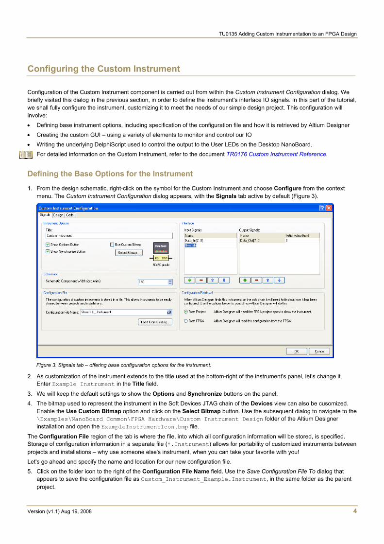
1. From the design schematic, right-click on the symbol for the Custom Instrument and choose Configure from the context menu. The Custom Instrument Configuration dialog appears, with the Signals tab active by default (Figure 3).
Figure 3. Signals tab – offering base configuration options for the instrument.
2. As customization of the instrument extends to the title used at the bottom-right of the instrument's panel, let's change it. Enter Example Instrument in the Title field.
3. We will keep the default settings to show the Options and Synchronize buttons on the panel.
4. The bitmap used to represent the instrument in the Soft Devices JTAG chain of the Devices view can also be cusomized. Enable the Use Custom Bitmap option and click on the Select Bitmap button. Use the subsequent dialog to navigate to the \Examples\NanoBoard Common\FPGA Hardware\Custom Instrument Design folder of the Altium Designer installation and open the ExampleInstrumentIcon.bmp file.
The Configuration File region of the tab is where the file, into which all configuration information will be stored, is specified. Storage of configuration information in a separate file (*.Instrument) allows for portability of customized instruments between projects and installations – why use someone else's instrument, when you can take your favorite with you!
Let's go ahead and specify the name and location for our new configuration file. 5. Click on the folder icon to the right of the Configuration File Name field. Use the Save Configuration File To dialog that
appears to save the configuration file as Custom_Instrument_Example.Instrument, in the same folder as the parent project.
TU0135 Adding Custom Instrumentation to an FPGA Design
Version (v1.1) Aug 19, 2008 5
When a custom instrument is detected in the Soft Devices JTAG chain, there are two methods by which Altium Designer can access the relevant configuration information: • From Project - the configuration information is retrieved from the corresponding .Instrument file for the instrument, which
resides alongside the project file. The project must be open in order to show the instrument from the Devices view. • From FPGA - the configuration information is downloaded with the design to the physical device, and stored in Block RAM.
It is retrieved directly from here and the project need not be open. 6. For this tutorial, let's have the configuration for the instrument stored in the target physical FPGA device. Enable the From
FPGA option in the Configuration Retrieval region of the tab.
The Signals tab of the dialog, now fully configured for our requirements, should look like the image in Figure 4.
Figure 4. Signals tab – fully configured for our design.
Designing the Custom GUI
Now it's time to create the GUI – the customized panel for the instrument that will be accessed once the design is programmed into the daughter board FPGA. 1. Click on the Design tab at the bottom of the Custom Instrument Configuration dialog. You will be presented with a 'shell'
instrument form with which to build the GUI (Figure 5).
Figure 5. Design tab – providing the canvas with which to create our custom GUI.
TU0135 Adding Custom Instrumentation to an FPGA Design
Version (v1.1) Aug 19, 2008 6
There are three tabbed panels associated to the form: - Palette – provides a range of standard scripting components and instrument-specific controls for use on the form
- Properties – displays all attributes of the currently selected control (or object) in the form
- Events – lists the applicable events for the currently selected control (or object) in the form. This tab is used to hook-up a script procedures or function to a control, which will be called when the specified event occurs.
The currently selected object in the form, named DesignedAreaPanel, represents the bounds of form design. We can only place controls and objects within this area.
2. We are going to add a variety of controls to the panel, so let's increase the area we have to work with. Increase the Height property for the DesignedAreaPanel object from 270 to 352.
Table 2 identifies the various instrument controls that we will use in our custom panel GUI and the corresponding entries in the Instrument Controls region of the Palette panel used to place them within the form.
Table 2. Instrument controls required in the custom instrument panel.
Control Control Name Placed from the Palette by Clicking...
Quantity
TInstrumentCaption 2
TInstrumentGauge 1
TInstrumentProgressBar
8
TInstrumentLEDsPanel 2
TInstrumentLEDDigits
1
TInstrumentGraph
1
TInstrumentNumericPanel 1
TInstrumentLabel 2
TInstrumentButton
1
3. Go ahead and place all of these controls within the form, as shown in Figure 6. Note that the only modification to default controls, at this stage, is to reduce the size of each Progress Bar control.
TU0135 Adding Custom Instrumentation to an FPGA Design
Version (v1.1) Aug 19, 2008 7
Figure 6. Initial controls added to the form.
Now the base controls are placed, we need to modify properties so that we get the panel looking just the way we want it. Let's consider each control in turn, in terms of the property adjustments to be made (from the Properties panel). For those controls we are using to monitor inputs, we will directly specify the signal to be hooked up to the control.
4. Click to select the top-left Caption control. Modify the following properties: - AutoSize: Disable - Caption: Change to DATA INPUT MONITORING
- Font » Color: Change to CaptionText
- Font » Height: Change to -11
- Font » Name: Change to Tahoma
- Style » fsItalic: Enable - Width: Change to 296
5. Click to select the Gauge control. Modify the following properties: - BigTicks » Color: Change to Lime
- BigTicks » Step: Change to 32
- Color: Change to Black
- Font » Color: Change to White
- Max: Change to 256
- MediumTicks » Color: Change to Silver
- MediumTicks » Step: Change to 16
- Needle » Kind: Change to gnkTearDrop
- Numbers » Step: Change to 32
- Position: Change to 0
- SignalName: Use the drop-down to assign the Data_In[7..0] input signal to this control
- SmallTicks » Color: Change to White
- SmallTicks » Step: Change to 8
6. Use shift+click to select all eight Progress Bar controls. Modify the following properties: - BarColor: Change to Yellow
- BarInactiveColor: Change to Gray
- BarMiddleColor: Change to Gray
TU0135 Adding Custom Instrumentation to an FPGA Design
Version (v1.1) Aug 19, 2008 8
- ColorScheme: This will automatically change to icsCustom by virtue of the color changes made
- Max: Change to 1
- Position: Change to 0
Starting with the left-most Progress Bar control, select each control in turn and set the SignalName property to assign the corresponding signal line of the Data_In[7..0] input. So set Data_In[7] for the leftmost control, then Data_In[6] for the next control, through to Data_In[0] for the right-most control.
7. Click to select the left-hand LEDs Panel control. Modify the following properties: - DigitsInGroup: Change to 8
- Metrics » EndSpace: Change to 1
- Metrics » Space: Change to 1
- Metrics » StartSpace: Change to 1
- SignalName: Use the drop-down to assign the Data_In[7..0] input signal to this control
8. Click to select the LED Digits control. Modify the following properties: - DigitsInGroup: Change to 8
- Metrics » Space: Change to 6
- SignalName: Use the drop-down to assign the Data_In[7..0] input signal to this control
9. Click to select the Graph control. Modify the following properties: - Color: Change to InfoBk
- SignalForm » NormalSignal » Color: Change to Red
- SignalName: Use the drop-down to assign the Data_In[7..0] input signal to this control
- Width: Change to 264
10. Click to select the top-right Caption control. Modify the following properties: - AutoSize: Disable - Caption: Change to DATA OUTPUT CONTROL
- Font » Color: Change to CaptionText
- Font » Height: Change to -11
- Font » Name: Change to Tahoma
- Style » fsItalic: Enable - Width: Change to 296
11. Click to select the Numeric Panel control. Modify the following properties: - Name: Change to Output_Data
- UseDefaultDigitClick: Enable
12. Click to select the InstrumentLabel1 control. Modify the following properties: - Caption: Change to NB_Override
- Font » Color: Change to Red
- Font » Height: Change to -13
- Name: Change to NB_Override
TU0135 Adding Custom Instrumentation to an FPGA Design
Version (v1.1) Aug 19, 2008 9
13. Click to select the InstrumentLabel2 control. Modify the following properties: - Caption: Change to Panel_Override
- Font » Color: Change to Red
- Font » Height: Change to -13
- Name: Change to Panel_Override
14. Click to select the right-hand LEDs Panel control. Modify the following properties: - Color: Change to 3DDkShadow
- Digits: Change to 1
- DigitsInGroup: Change to 1
- SignalName: Use the drop-down to assign the Override input signal to this control
- Style: Change to icsGreen
15. Click to select the Button control. Modify the following properties: - AllowAllUp: Enable - Caption: Enter SOFTWARE OVERRIDE
- Font » Height: Change to -13
- Style » fsBold: Enable
- Style » fsItalic: Enable - GroupIndex: Change to 1
- Height: Change to 48
- Name: Change to Panel_Override_Button
- Width: Change to 200
Having made these changes, the instrument panel form should now appear as shown in Figure 7.
Figure 7. Panel controls after modification of properties.
Let's finish off the design of the instrument panel by adding a few descriptive labels. We will add labels next to the Graph control for the High and Low threshold values and various labels to describe the operation of the controls on the panel.
16. Add InstrumentLabel controls with captions and placement as shown in Figure 8. In each case, disable the AutoSize property and size the label accordingly.
TU0135 Adding Custom Instrumentation to an FPGA Design
Version (v1.1) Aug 19, 2008 10
Figure 8. Finished instrument panel design, complete with descriptive labeling.
We have now finished designing our custom panel, in terms of controls and aesthetics. For the controls used to monitor incoming signals to our custom instrument, we have directly assigned the input signal to the relevant control. For data output however, our design requires a bit more 'smarts' in terms of how the data to the User LEDs on the Desktop NanoBoard is controlled. For this, we need to turn to scripting to achieve the requirements of our simple design.
Writing the Script
Before we look at the script itself, let's recap what we want to have happen, in relation to the data output from our custom instrument:
• In normal operation, the output should be placed under the control of the Numeric Panel control. • If either the 'DAUGHTER BD TEST/RESET' button on the Desktop NanoBoard, or the SOFTWARE OVERRIDE button on the
instrument panel is pressed, the Numeric Panel should be overriden. The value output should be zero, and the corresponding message appear on the instrument panel, to alert the user to which override has been engaged.
1. Click on the Code tab at the bottom of the Custom Instrument Configuration dialog. You will be presented with a blank page on which to write the content of your script (Figure 9).
Figure 9. Code tab – providing an area to develop your DelphiScript code.
TU0135 Adding Custom Instrumentation to an FPGA Design
Version (v1.1) Aug 19, 2008 11
Note: Only DelphiScript is supported when writing script for a custom instrument. Should you wish to write your script within the comfort of a code-aware editor within Altium Designer, simply click the Open in Code Editor button at the bottom of the dialog. This allows you to take advantage of the syntax highlighting and related code-based features available in the editor, that are not available in the Code tab of the dialog.
If you use the Code Editor to write your script, simply save the file when done and the code will be available in the dialog when next accessed.
2. Type the following script. The comments can of course be omitted, but it is always good practice to comment code and, for the purposes of this tutorial, highlight what the script is being used to achieve.
//The following procedure is entered when a read or write event occurs within the area of the //designed panel
Panel_Override_Button.Down := not Panel_Override_Button.Down;
end;
TU0135 Adding Custom Instrumentation to an FPGA Design
Version (v1.1) Aug 19, 2008 12
IO values are updated by nature of the polling, not by the OnReadWrite event. The latter is simply a method to synchronously call code which can process the signal values at each poll point.
Hooking the Script up to the GUI We have our designed instrument panel. We have our DelphiScript code to achieve the desired manipulation of the output. We now need to hook our script up to the GUI, so that the relevant procedure can be called when a certain event occurs within the panel.
Each component/control has a number of events associated with it. These are the events that the component/control can 'react' to. The script code that gets used when an event is 'fired' is that event's handling code. The parent procedure or function written in the script is therefore the 'event handler'. The logical place then, to link event to event handler, is the value of the event – defined on the Events panel, when the Design tab of the dialog is active.
When monitoring inputs or controlling outputs – wired to the Custom Instrument – we are dealing with not just a single control object on the instrument's panel, but rather the entire panel itself. The event we are interested in, and to which we will link our code to write values onto the Data_Out line, is the OnReadWrite event.
The panel's OnReadWrite event is hard coded to 'fire' each time the instrument polls. The polling interval is 250ms by default, and can be changed in the Custom Instrument – Options dialog (accessed by clicking on the Options button included on the panel).
Each time the instrument polls, the current value for each input signal is read into an internal storage structure. Similarly, the current value internally stored for each output signal is made available at the corresponding output pin of the instrument. The internal storage structure is transparent to the user and, as such, cannot be accessed in any way. The event handling code linked to the OnReadWrite event is essentially used to process the IO as required.
Figure 10. Use event handling code linked to the panel's OnReadWrite event to process signal IO each time the instrument polls.
If polling is turned off (by setting the Update value in the Custom Instrument – Options dialog to 0ms), the OnReadWrite event will not fire. It will, however, fire if the Synchronize button is available on the instrument's panel, and is pressed. This would essentially be a 'manual poll'.
Let's go ahead and hook up our two scripting procedures to the relevant objects and events. 1. Open the Custom Instrument Configuration dialog (if not already) and make the Design tab active.
2. Click anywhere within the bounds of the panel, away from controls, to select the DesignedAreaPanel object. 3. From the associated Events panel, click inside the field to the right of the OnReadWrite event and use the drop-down to
choose (and assign) the DesignedAreaPanelReadWrite procedure.
4. Now click to select the SOFTWARE OVERRIDE Button control. 5. In the associated Events panel, click inside the field to the right of the OnClick event and use the drop-down to choose (and
assign) the Panel_Override_ButtonClick procedure.
That's it. We have completely finished configuring our custom instrument. Time to target and program the physical FPGA device with our design, so that we can see it in action!
TU0135 Adding Custom Instrumentation to an FPGA Design
Version (v1.1) Aug 19, 2008 13
Targeting the Physical FPGA Device
Now we are finished with the capture phase of our design, we need to specify which physical FPGA device we want to use – the target for our design and the end medium into which the design will ultimately be programmed and run. For this tutorial, we will target an FPGA device located on a 3-connector daughter board that is plugged into the Desktop NanoBoard NB2DSK01.
The easiest way to configure the project is to use Altium Designer's auto-configuration feature This will configure the project based on the exact hardware present in your Desktop NanoBoard system. Let's go ahead and configure our FPGA project.
1. Ensure the 3-connector daughter board carrying the FPGA device to which the design will be targeted is plugged into the NB2DSK01 motherboard.
2. Our simple custom instrument design does not use any resources resident on plug-in peripheral boards. These boards can be left attached to the motherboard, or removed, as desired.
3. Ensure your Desktop NanoBoard is connected to the PC via USB (or parallel) connection and is powered-on.
4. Run the auto-configuration process on the project (Custom_Instrument_Design.PrjFpg).
5. When configuration is complete, save all source files and the parent project.
For more information on the concept of configurations and constraints, and their role in design portability, refer to the article AR0124 Design Portability, Configurations and Constraints.
For more detailed information on the Desktop NanoBoard NB2DSK01 constraint system, including auto-configuration, refer to the application note AP0154 Understanding the Desktop NanoBoard NB2DSK01 Constraint System.
Processing the Design
Now that the design has been fully captured and targeted to our daughter board FPGA device, we can go ahead and process the design – ultimately creating the required FPGA programming file with which to program the target device.
1. Ensure that your Desktop NanoBoard is connected to your PC and powered on. 2. Ensure that the Devices view is the active view within Altium Designer and that the Live option is enabled and the
Connected indicator is Green.
3. In the associated 'Process Flow' for the physical device, click on the Program FPGA button – the last stage in the flow. The design will be compiled, synthesized and the vendor tools invoked. Ultimately the FPGA programming file will be generated and downloaded, via JTAG, to the physical device on the daughter board.
Once the design has been downloaded, the text underneath the physical device's icon in the Devices view will change from Reset to Programmed. On the hardware side, the 'Program' LED on the daughter board will be lit (Green), confirming the design has been loaded into the physical device.
For more information on the Process Flow and the Devices view, refer to the document AP0103 Processing the Captured FPGA Design.
Figure 11. Auto-configure direct from Devices view.
Figure 12. Starting the programming process.
TU0135 Adding Custom Instrumentation to an FPGA Design
Version (v1.1) Aug 19, 2008 14
Accessing the Customized Instrument Panel
Now the design has been programmed into the physical FPGA device, we can finally access the customized GUI we created for the instrument in real-time. This is the exciting final part of our tutorial – the part where we get to 'play' with the fruits of our labor! 1. In the Devices view, notice that the customized icon for our instrument has appeared in the Soft Devices JTAG chain, which
only gets presented in the view once the design is programmed into the physical FPGA device. The status of the instrument should appear as 'Running'.
2. Double-click on the icon for the Custom Instrument. The associated instrument panel – our custom GUI – will appear in the Instrument Rack – Soft Devices panel.
Figure 14. Accessing our customized GUI.
3. Turn various switches associated to the Desktop NanoBoard's DIP-Switch ON and OFF and observe that the same value is reflected in the various monitoring controls that we added and defined for the panel:
- The Gauge
- The Progress Bars
- The LEDs Panel
- The LED Digits
- The Graph.
4. Use the Numeric Panel control and click to toggle bits ON and OFF. Observe that the corresponding LEDs on the Desktop NanoBoard will toggle in their lit status accordingly.
5. Set the lower nibble of the Numeric Panel control to '1111', causing User LEDs 3..0 to become lit on the NanoBoard.
Figure 13. Monitoring the input value from the DIP-switch.
TU0135 Adding Custom Instrumentation to an FPGA Design
Version (v1.1) Aug 19, 2008 15
6. Momentarily press the 'DAUGHTER BD TEST/RESET' button on the NanoBoard. Observe that:
- User LEDs 3..0 switch OFF
- The associated hardware override message appears on the instrument panel
- The LED on the instrument panel used to monitor the state of the 'DAUGHTER BD TEST/RESET' button becomes lit.
7. Now press the SOFTWARE OVERRIDE button on the
instrument panel. Observe that:
- User LEDs 3..0 switch OFF again
- The associated software override message appears on the instrument panel.
8. Click on the SOFTWARE OVERRIDE button again to disengage the override and observe the User LEDS 3..0 become lit again.
That concludes this tutorial. We have only really scratched the surface with respect to the functionality and power that the Custom Instrument has to offer. Now, armed with a basic understanding of its use, you can embark on more complex designs, confident in the knowledge that this fully customizable instrument delivers the required 'grunt' to facilitate your digital IO monitoring and control requirements.
Figure 15. Invoking the hardware override.
Figure 16. Invoking the software override.
TU0135 Adding Custom Instrumentation to an FPGA Design
Version (v1.1) Aug 19, 2008 16
Revision History
Date Version No. Revision
17-May-2008 1.0 Initial release
19-Aug-2008 1.1 Updated images relating to the Custom Instrument Configuration dialog. Enhanced information for section 'Hooking the Script up to the GUI'.
02-Aug-2011 - Updated template.
Software, hardware, documentation and related materials:
All rights reserved. You are permitted to print this document provided that (1) the use of such is for personal use only and will not be copied or posted on any network computer or broadcast in any media, and (2) no modifications of the document is made. Unauthorized duplication, in whole or part, of this document by any means, mechanical or electronic, including translation into another language, except for brief excerpts in published reviews, is prohibited without the express written permission of Altium Limited. Unauthorized duplication of this work may also be prohibited by local statute. Violators may be subject to both criminal and civil penalties, including fines and/or imprisonment.
Altium, Altium Designer, Board Insight, DXP, Innovation Station, LiveDesign, NanoBoard, NanoTalk, OpenBus, P-CAD, SimCode, Situs, TASKING, and Topological Autorouting and their respective logos are trademarks or registered trademarks of Altium Limited or its subsidiaries. All other registered or unregistered trademarks referenced herein are the property of their respective owners and no trademark rights to the same are claimed.