Additive Manufacturing of Smart Parts with Embedded Sensors for In-Situ Monitoring in Advanced Energy Systems DE-FE0012272 Investigators: Hai-Lung Tsai (PI), Ming Leu, Missouri S&T Hai Xiao, Clemson University Junhang Dong, University of Cincinnati Program Manager: Richard Dunst and Otis Mills, NETL NETL Crosscutting Technology Research Review Meeting, Pittsburgh, PA, March 20, 2017
Transcript
Additive Manufacturing of Smart Parts with Embedded Sensors for In-Situ Monitoring in
Advanced Energy SystemsDE-FE0012272
Investigators: Hai-Lung Tsai (PI), Ming Leu, Missouri S&THai Xiao, Clemson UniversityJunhang Dong, University of Cincinnati
Program Manager: Richard Dunst and Otis Mills, NETL
NETL Crosscutting Technology Research Review Meeting, Pittsburgh, PA, March 20, 2017
Outline
• Introduction
• Technical Progresses and Accomplishments
• Summary
• Future Work
Demands
• Sensors and instrumentation are needed in advanced energy systems for – Advanced process control/optimization– Health status monitoring of key components– System maintenance and lifecycle management
• Sensors need to survive and operate in the high-T, high-P and corrosive/erosive harsh environments for a long time
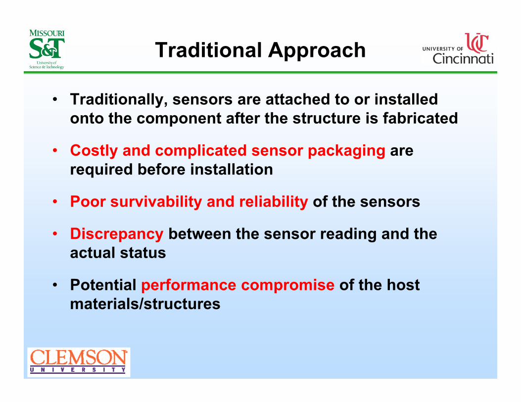
Traditional Approach
• Traditionally, sensors are attached to or installed onto the component after the structure is fabricated
• Costly and complicated sensor packaging are required before installation
• Poor survivability and reliability of the sensors
• Discrepancy between the sensor reading and the actual status
• Potential performance compromise of the host materials/structures
Opportunities
• Smart parts – widely used and proven successful in civil engineering for structural health monitoring (SHM)
• Provide the real-time information of the component and system
• Reduce the complexity in sensor packaging and installation
• Increase the robustness and reliability of the system
Objectives• Main Objective: Demonstrate the new concept of sensor-
integrated “smart part” achieved by additive manufacturing and embedding microwave and photonic sensors into critical components used in advanced energy systems
• Specific objectives– Robust, distributed and embeddable microwave photonic sensors – Additive manufacturing techniques for rapid fabrication of “smart
parts” and sensors embedment– Multifunctional transition layer between the embedded sensor and
host material for sensor protection and performance enhancement– Models to correlate the sensor readings with the parameters of
interest– Sensor instrumentation for in situ and distributed measurement– Feasibility tests and performance evaluation
Project Elements/Overview
• Performers: Missouri S&T, Clemson, University of Cincinnati
• Interdisciplinary team – Hai-Lung Tsai (PI), Professor of Mechanical Engineering, Missouri S&T,
Modeling and AM of metal parts– Ming Leu, Professor of Mechanical Engineering, Missouri S&T, AM of
ceramic parts– Hai Xiao, Professor of Electrical Engineering, Clemson University, Sensors
and Instrumentation, test and evaluation– Junhang Dong, Professor of Chemical Engineering, University of Cincinnati,
Sensor protections
• Success criteria: – Demonstrate concept and capability in simulated laboratory environments
Development of robust, distributed and embeddable sensors and
• Three types of fully distributed sensors for embedded applications
1. Microwave sensors – uniquely harvest the robustness of high temperature coaxial cables
2. Incoherent Optical carrier based microwave interferometry (OCMI) sensors – can be used to interrogate previously difficult highly multimode fibers (e.g., quart rod and sapphire fiber)
3. Coherent OMCI sensors – can reach extremely high resolution
Page 9
Microwave-Photonics Sensors• Optical carrier based microwave interferometry (OCMI)
– Read optical interferometers using microwave– Optics as the carrier to perform measurement– Microwave as the signal to locate the sensors– Can be implemented in either incoherent (make the optical
term become zero) or coherence (keep the optical term)
Page 10
Microwave term
Optical term
max
min
2 2 2 2 1 2 1 21 2
2 1 2 1 2
22 2 cos cos2 2
2 1 cos 1 cos cos
O O O O
O O O O
L L W L LE E E A A M tc c
W L W L L LA M t M t dc c c
J. Huang, et al., Optics Express, 2014.
Quartz rod (800m dia. Uncladded)
Fused silica rod 800m dia.
High temperature response
R13dB coupler
Input
Output
Path 2
Path 1
R2
18.7 cm
Large core fiber
Interference fringes
Quartz rod can be used to measure strains at high temperaturesL. Hua., Applied Optics, 2015
Sapphire Michelson Sensor (125 µm)
Page 12
1000 1500 2000 2500 3000 3500 4000 4500
-60
-50
-40
-30
Am
plitu
de (d
B)
Frequency (MHz)
Joint by fusion
R1
3dB multimode fiber coupler
Input
Output
Joint by fusion
R2
10.2 cm
Silica graded-index multimode (62.5 m core and 125 m cladding)
Single crystal sapphire fiber (125 m diameter, uncladded)
• Use a coherent light source • Arrange the interferometers within the coherent length
of the source
Page 14
Very high resolution • Use both real and imaginary part of the signal (quadrature) • Resolution reaches 10n using an interferometer with a
length of 10cm.
Incoherent and Coherent OCMI
• Incoherent OCMI – use incoherent (i.e., broadband) optical source – Large dynamic range – Resolution is limited, about 10-5 - 10-6
• Coherent OCMI – use coherent (i.e., narrow bandwidth) optical source – Limited dynamic range – Resolution can be extremely high, about 10-8 - 10-9
• The two can be combined into a single system with two optical sources to achieve a high resolution in a large dynamic range. – Sensing Range (Spatial resolution): 100 km(1m), 2km(2cm)
Page 16
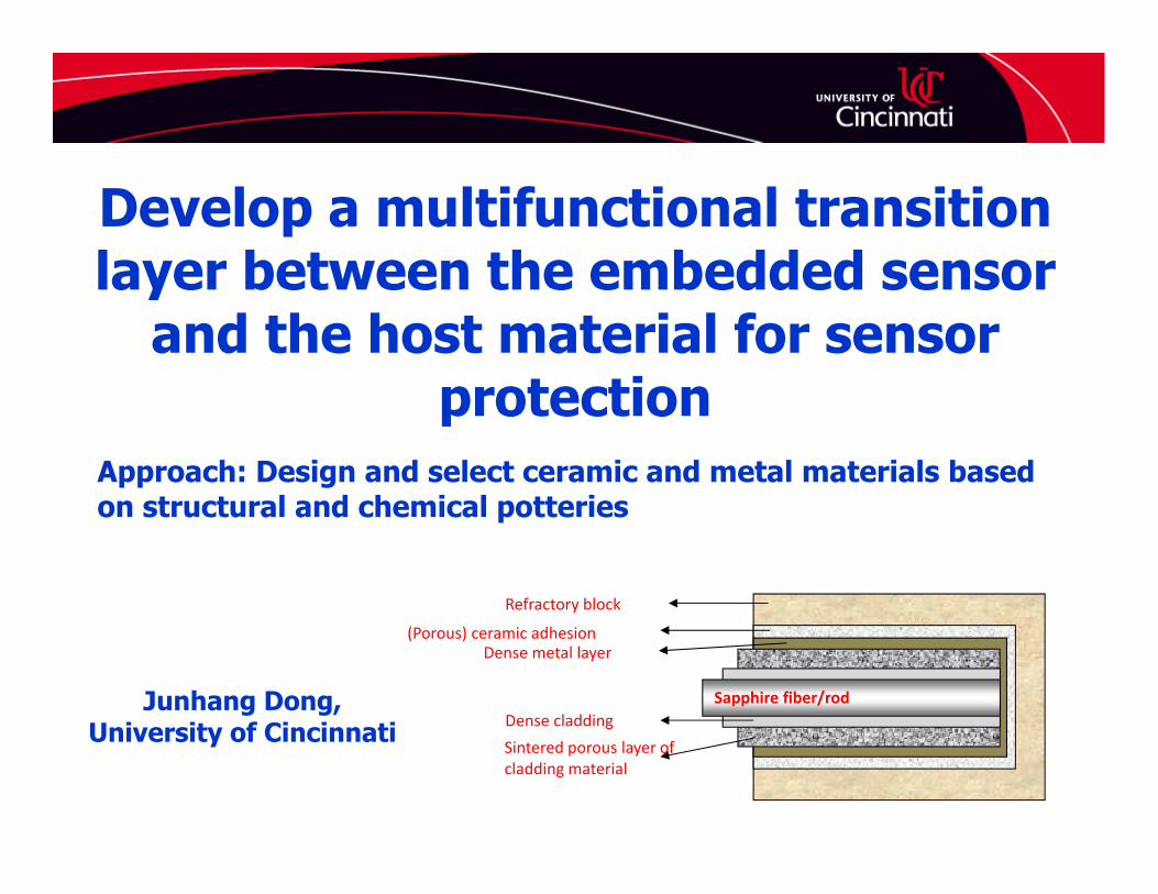
Develop a multifunctional transition layer between the embedded sensor
and the host material for sensor protection
Sapphire fiber/rodDense claddingSintered porous layer of cladding material
Dense metal layer(Porous) ceramic adhesion
Refractory block
Approach: Design and select ceramic and metal materials based on structural and chemical potteries
Junhang Dong, University of Cincinnati
Summary of Accomplishments
• Silica fiber optic sensors packaged in the ceramic host capillary tubes are fully functional at high temperature (tested up to 1000oC) with good stability
• Silicalite layers directly grown on the sapphire fibers may be used both as fiber cladding and sensor protection (up to ~900oC)
• MgAl2O4 layers can be used as sapphire cladding for operation up to 1250oC.
Interface Stability in Layered Structure for Sensor Protection
Results: Stainless steel has been identified as the most stable metal among the candidates (Ti/Pd, Al, Cu, etc.) and demonstrated to be stable when coated with ceramics at 1000oC for >100h
Silicalite surface
MgAl2O4surface
Spinal MgAl2O4
Silicalite
Stainless steel
Sensor Protection by ceramic adhesive in sintered SS capillary tube
Stainless steel hosted fiber unit:
Fused silica optical fibers as a packaged sensor unit for direct installation in “smart bricks”. Porous ceramic adhesion layers (e.g. alumina and zirconia based materials) used to fix the fiber with the host capillary tube.
EDS line scan across the SS/alumina interface/fiber interfaces indicated no significant solid state reaction or diffusion at 1000oC over extended period.
Multilayer-Protected FOS FabricationResults: pre-packaging of fibers in ceramic capillary tubes (e.g. porous zirconia and α-alumina) has been demonstrated using ceramic adhesion and tested at 1000oC stable over extended periods.
Zirconia tube
α-aluminafilling
Opticalfiber
Zirconia
Alumina
Optical Fiber alumina
Sensor Protection by ceramic adhesive in ceramic capillary tube
Packaging of Fiber Optic Sensor in Host Ceramic (or SS) Capillary Tubes
ZAlMgADZ
ADZ
Optical Functionality Tests for the Fiber Sensor in Capillary Tables
Results: The fibers pre-packaged in the host tubes have been verified to be optically functional for signal generation and transmission at high temperatures
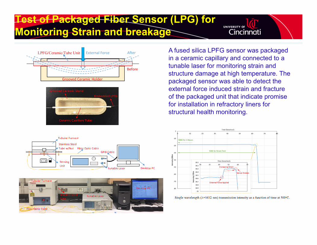
Test of Packaged Fiber Sensor (LPG) for Monitoring Strain and breakage
External Force
Grooved Ceramic Holder
LPFG/Ceramic/Tube Unit
Before
After A fused silica LPFG sensor was packaged in a ceramic capillary and connected to a tunable laser for monitoring strain and structure damage at high temperature. The packaged sensor was able to detect the external force induced strain and fracture of the packaged unit that indicate promise for installation in refractory liners for structural health monitoring.
Long-Term Stability of Sapphire Multilayer Protection
The structures of silicalite-coated-sapphire with an overcoats of ZAlMg (ZrO2-Al2O3-MgO mixture) and ADZ (Zr1-0.75xAlxSiO4) are both stable after firing at 1000oC for 200 h according to SEM and EDS examinations –No structural damage or inter-layer element diffusion was found.
Silicalite
Sapphire
AZlMg
Silicalite
Sapphire
ADZ
Additive Manufacturing of Ceramics
Approach: Multi-extruder freeze-form extrusion based additive manufacturing
Ming LeuMissouri University of Science and Technology
o A new ceramic on-demand extrusion (CODE) system has been developed to fabricate Functionally Graded parts (Configuration 1) and Multi-Material parts (Configuration 2).
Config. 1FGM
printing
Config. 2Multi-
materialprintingBuilding envelop: 250 x 250 x 150 mm3
Positioning resolution: 1 μmPositioning accuracy: 18 μm over 300 mm travel
Fabricating Parts with Support Material
Printing Post processing
(a) CAD model(b) Support structure being printed(c) Overhanging structure being printed(d) Part having been printed completely
(surrounded by oil)
(a) Parts after 1st step sintering(1100 °C)
(b) Support structures being dissolved(c) Cleaned parts (after support removal)(d) Final sintered parts
Sample Parts Fabricated with the CODE System
1 cm
Zirconia gears:400 μm layer98.5% Density
Alumina disks:400 μm layer
vs.200 μm layer
Alumina turbine blower housing400 μm layer, 97.5% density
Good circularityD1: Mean = 29.3 mm, Std.Dev. = 0.07 mmD2: Mean = 63.7 mm, Std.Dev. = 0.05 mm
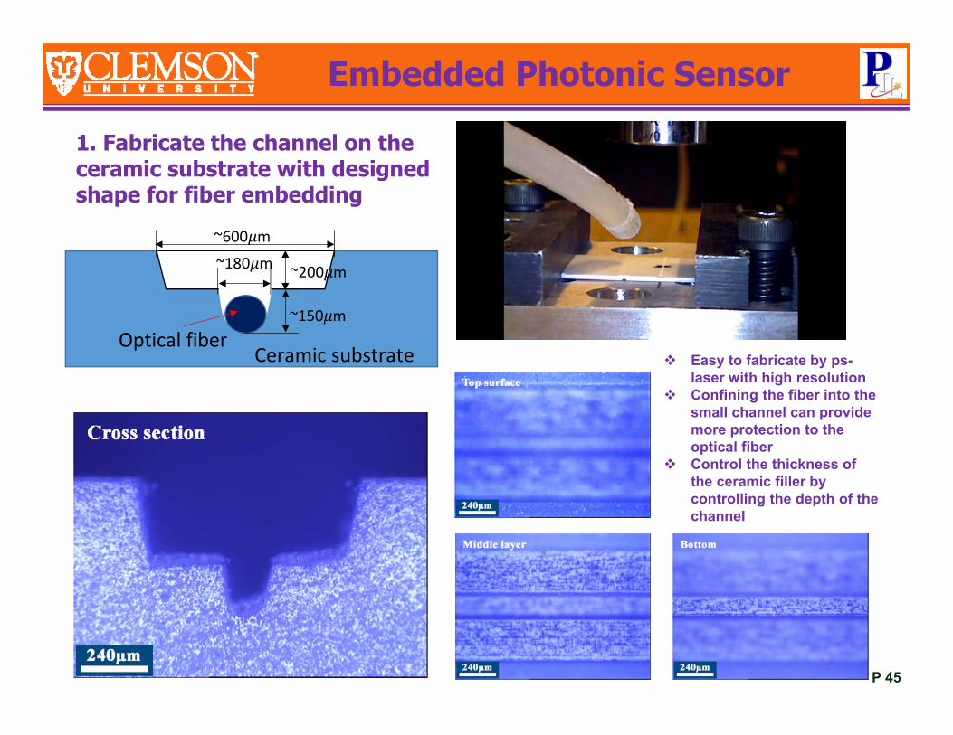
1. Fabricate the channel on the ceramic substrate with designed shape for fiber embedding
Ceramic substrateOptical fiber
~600 m
~200 m
~150 m
~180 m
Easy to fabricate by ps-laser with high resolution
Confining the fiber into the small channel can provide more protection to the optical fiber
Control the thickness of the ceramic filler by controlling the depth of the channel
Embedded Photonic Sensor
P 46
2. Place the optical fiber sensor into the channel and filled the channel with the ceramic paste
Fiber embedded setup An IFPI was placed inside the channel
Slightly applied tensile stress on two ends of the optical fiber to make sure it was straight and touch the bottom of the channel
Top view at the edge
Channel was filled with the ceramic paste
Embedded Photonic Sensor
P 47
Schematic of the CO2 laser processing system
3. Use a CO2 laser to process the filling materials and seal the fiber inside Laser operating parameters:• Laser output power: 9 W• Scanning speed: 0.2 mm/s• Spot size: 1.1 mm high speed scanning at low
power to pre‐heat the materials before high power processing
The optical fiber was monitoring by the OSA during the whole embedding process
Max Output Power 20W
Operation Continuous wave (CW)
Mode Quality TEM00, M2 < 1.1 ± 0.1
Beam Diameter before focusing 2.5mm ± 0.5mm
Beam Diameter after scanner ~1.0 mm
Wavelength 10.6 μm
Polarization Linear (Horizontal)
CO2 laser specification
Embedded Photonic Sensor
P 48
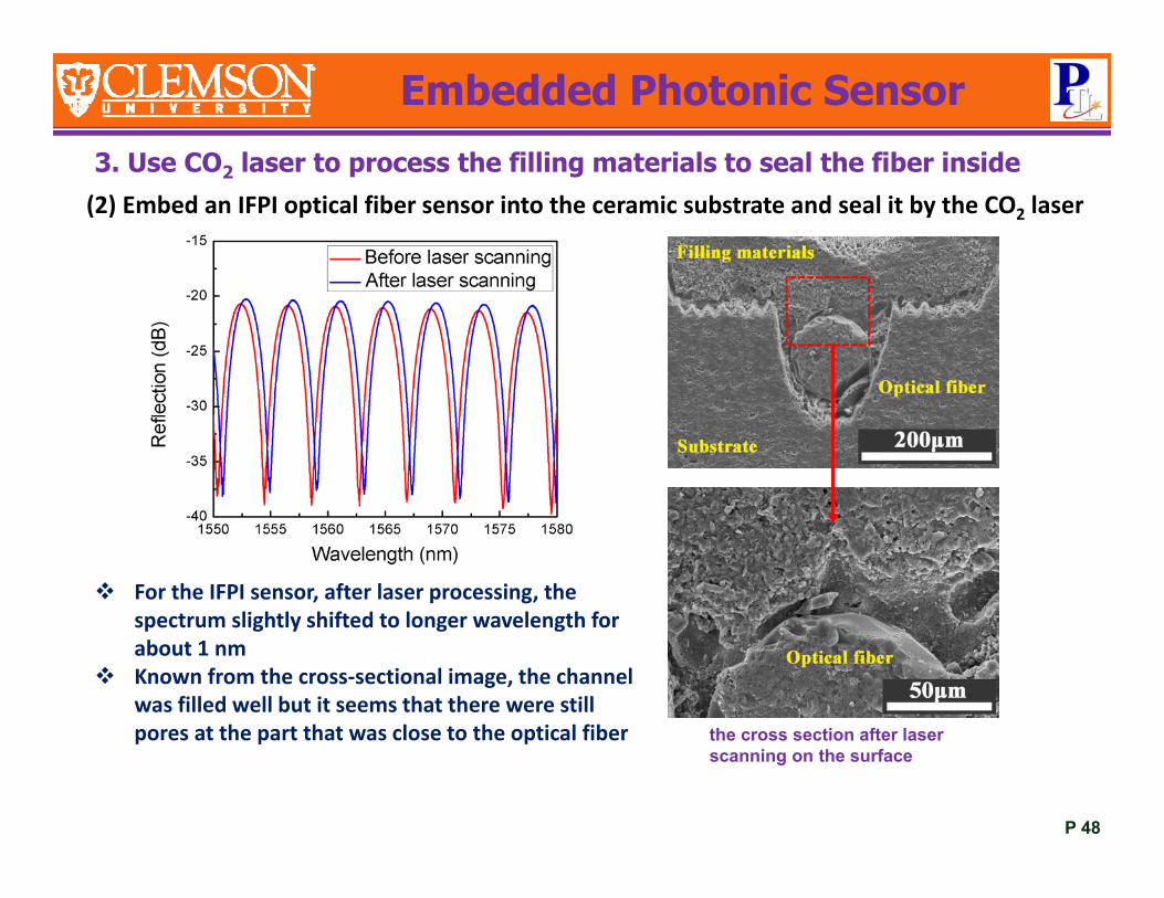
3. Use CO2 laser to process the filling materials to seal the fiber inside
For the IFPI sensor, after laser processing, the spectrum slightly shifted to longer wavelength for about 1 nm
Known from the cross‐sectional image, the channel was filled well but it seems that there were still pores at the part that was close to the optical fiber
(2) Embed an IFPI optical fiber sensor into the ceramic substrate and seal it by the CO2 laser
the cross section after laser scanning on the surface
Embedded Photonic Sensor
P 49
4. Test the high temperature stability of the embedded optical fiber sensor
Traditional furnace based sintering, the embedded optical fiber had a huge loss (~45 dB) when the temperature reached 400
Direct laser sintering, though small ripples occurred after 400 , the transmission spectrum generally maintain straight and only 5 dB loss when the temperature reached 1000
(1) Improved high temperature stability of the embedded optical fiber by laser sintering
Cross section after tested at 1000Direct laser sintering (successful) Furnace sintering (failed)Furnace sintering (failed)
Embedded Photonic Sensor
P 50
4. Test the high temperature stability of the embedded optical fiber sensor
(2) High temperature stability of the embedded intrinsic Fabry‐Perot interferometer (IFPI)
Survived 1000 and still produced good signals Slightly compression of the optical fiber that reduced the cavity length of
the IFPI Need further improvement and optimization
Manufacturing of smart parts• Manufacturing of sensor embedded smart parts (a smart
ceramic washer)
P 51
Embedded Photonic Sensor
P 52
Embedment and experimental setup
Large size
Ceramic block (φ = 8 cm)
Ceramic tube to guide fiber
Small size
Experimental setup
Ceramic block (φ = 5 cm)
1 2 3 4 5 6 7 8 9 10
-120
-110
-100
-90
-80
-70
-60
-50
Frequency (GHz)
Ref
lect
ion
(dB)
Embedded Photonic Sensor
Frequency domain Frequency response VS temperature
Distributed microwave and photonic sensors and instrumentation have been developed and proven
Protective coating materials have been identified and successfully coated on silica and sapphire optical fibers
Additive Manufacturing techniques have been developed for fabrication of metal and ceramic parts
Smart parts with embedded sensors have been fabricated using advanced manufacturing and preliminarily tested
P 54
Future Work
• Manufacture more smart parts
• Comprehensive tests of the smart parts
P 55
Acknowledgement
• NETL Managers and Engineers (current and former) – Robert Romanosky– Susan Maley– Robie Lewis– Steve Seachman– Barbara Carney – Sydni Credle – Paul Ohodnicki– Benjamin Chorpening – Richard Dunst– Jessica Mullen – Otis Mills