ouse, 32 Southtoown Road, Great YYarmouth, Norfoolk, England, NR31 ODU
lovickm
Stamp
lovickm
Stamp
lovickm
Rectangle
BOOKBINDING AREA
DOC.DATASHEET STATEMENT
The following icons are absolutely designed by Midas independently in 2007-SEP. They are not in commonuse in the LCD industry yet but just used for marking out Midas products’ characteristics quickly andsimply without any special meaning. Midas reserves the composing right and copyright.No one else is allowed to adopt these icons without Midas approval.
1.
The ISO9001 logo used in this document is authorized by SGS (www.sgs.com). Midas had alreadysuccessfully passed the strict and professional ISO9001:2000 Quality Management System Certification andgot the certificate (No.: CN07/00404)
2.
The technologies/techniques/crafts which denoted by the following icons are not exclusively owned by Midas,but also shared by Midas LCD strategic cooperators, however all these technologies/techniques/crafts havebeen finally confirmed by Midas professional engineers and QC department.
3.
SAMPLE APPROVAL document rather than consider this DATASHEET as the standard for judging whether or not theLCD meets your requirements. Once you instruct Midas to a mass-production without definite demand forproviding sample before, Midas will disclaim all responsibility if the mass-production is proved not meeting withyour requirements.
As the difference in test standard and test conditions, also Midas insufficient familiarity with the actual LCDusing environment, all the referred information in this DATASHEET (including the icons) only have two functions:4.1: providing quick reference when you are judging whether or not the product meets your requirements.4.2: listing out definitely the tolerance.
4.
The sequence of the icons is random and doesn’t indicate the importance grade.5.
Icons explanation6.
This icon on the cover indicates the productis with high contrast; Otherwise not.
HIGH CONTRAST LONG LIFE VERSIONThis icon on the cover indicates the productis long life version (over 9K hours guaranteed);Otherwise not.
H C
3.0VVlcm = 3.0V
This icon on the cover indicates the productcan work at 3.0V exactly; otherwise not.
3TIMEs 100% QC EXAMINATIONThis icon on the cover indicates the producthas passed Midas thrice 100% QC.Otherwise not.
This icon on the cover indicates the LED had passedMidas twice strict selection which promises theproduct’s identical color and brightness; Otherwise not.
TWICE SELECTION OF LED MATERIALS
This icon on the cover indicates the productis with high response speed; Otherwise not.
FAST RESPONSE TIME
This icon on the cover indicates the productis with protection circuit; Otherwise not.
PROTECTION CIRCUIT
FFF
Y C
X C
OPERATION TEMPERATURE RANGE
This icon on the cover indicates the operatingtemperature range (X-Y).
This icon on the cover indicates the productmeets ROHS requirements; Otherwise not.
RoHS COMPLIANCE
RoHS
Midas 2006 version logo.Midas is an integrated manufacturer of flatpanel display (FPD). Midas supplies TN, HTN, STN, FSTN monochromeLCD panel; COB, COG, TAB LCD module; and all kinds of LED backlight.
WIDE VIEWING SCOPE
This icon on the cover indicates the productis with wide viewing scope; Otherwise not.
Anti UV VERSION
This icon on the cover indicates the productis against UV line. Otherwise not.
UV
N New structure, new craft, newtechnology and new materials inside both LCDmodule and LCD panel to improve the "RainBow"
N SERIES TECHNOLOGY (2008 developed)
Page 2 , Total 28 Pages
MC22405C6WK-BNMLW
Contents 1. Specification Revision History Page 3 2. General Specification Page 4 3. Module Classification Information Page 5 4. Interface Pin Function Page 6 5. Contour Drawing & Block Diagram Page 7 6. Function Description Page 8 7. Character Generator ROM Pattern Page 11 8. Instruction Table Page 12 9. Timing Characteristics Page 13 10. Initializing of LCM Page 15 11. Optical Characteristics Page 17 12. Absolute Maximum Ratings Page 18 13. Electrical Characteristics Page 18 14. Backlight Information Page 19 15. Reliability Page 20 16. Inspection specification Page 21 17. Precautions in use of LCD Modules Page 25 18. Material List of Components for RoHs Page 26
Page 3 , Total 28 Pages
1. Specification Revision History
RECORDS OF REVISION
VERSION DATE REVISED PAGE NO. Note
1
2008.04.07
First issue
Page 4 , Total 28 Pages
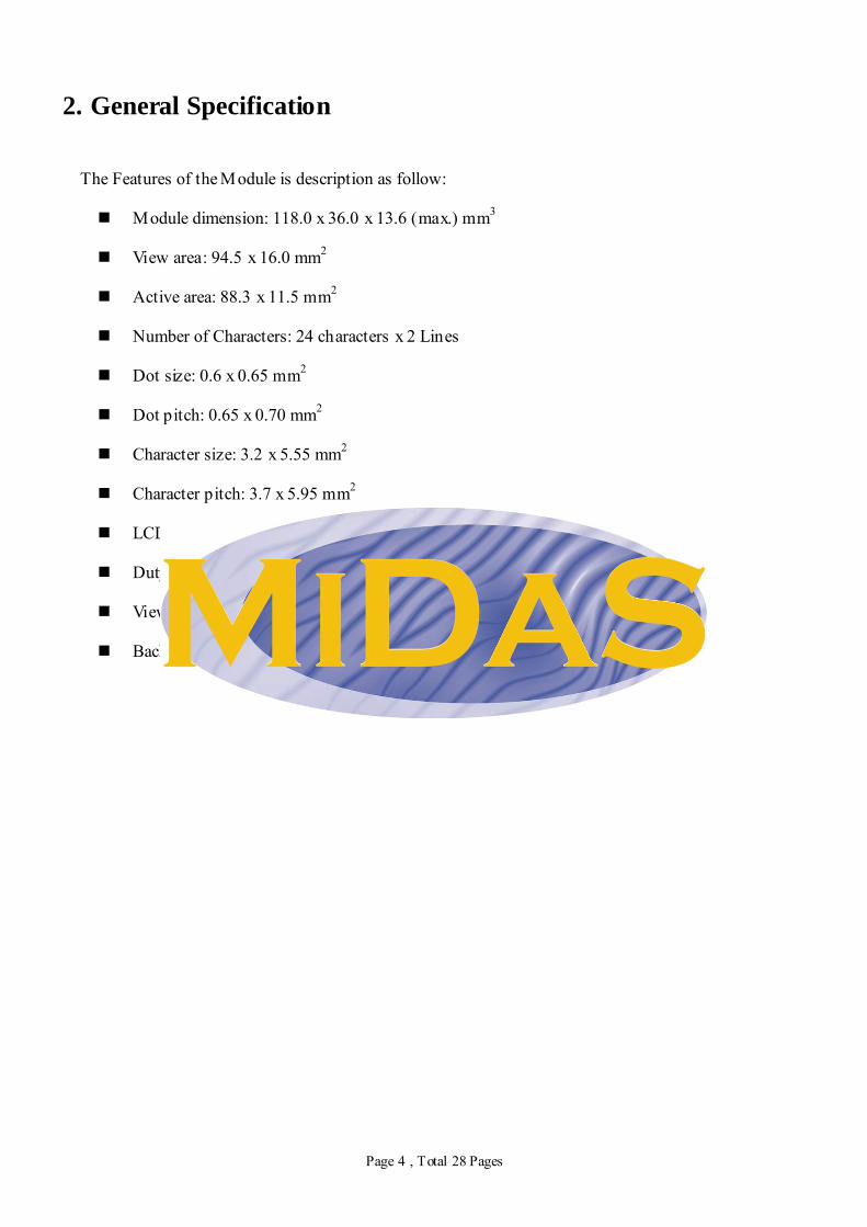
2. General Specification
The Features of the Module is description as follow:
Module dimension: 118.0 x 36.0 x 13.6 (max.) mm3
View area: 94.5 x 16.0 mm2
Active area: 88.3 x 11.5 mm2
Number of Characters: 24 characters x 2 Lines
Dot size: 0.6 x 0.65 mm2
Dot pitch: 0.65 x 0.70 mm2
Character size: 3.2 x 5.55 mm2
Character pitch: 3.7 x 5.95 mm2
LCD type: STN, Negative, Transmissive , blue
Duty: 1/16
View direction: 6 o’clock
Backlight Type: LED White
Midas LCD Part Number System
MC COG 132033 A * 6 W * * - S N T L W * *
1 2 3 4 5 6 7 8 9 - 10 11 12 13 14 15 16
1 = MC: Midas Components
2 = Blank: COB (chip on board) COG: chip on glass
3 = No of dots (e.g. 240064 = 240 x 64 dots) (e.g. 21605 = 2 x 16 5mm C.H.)
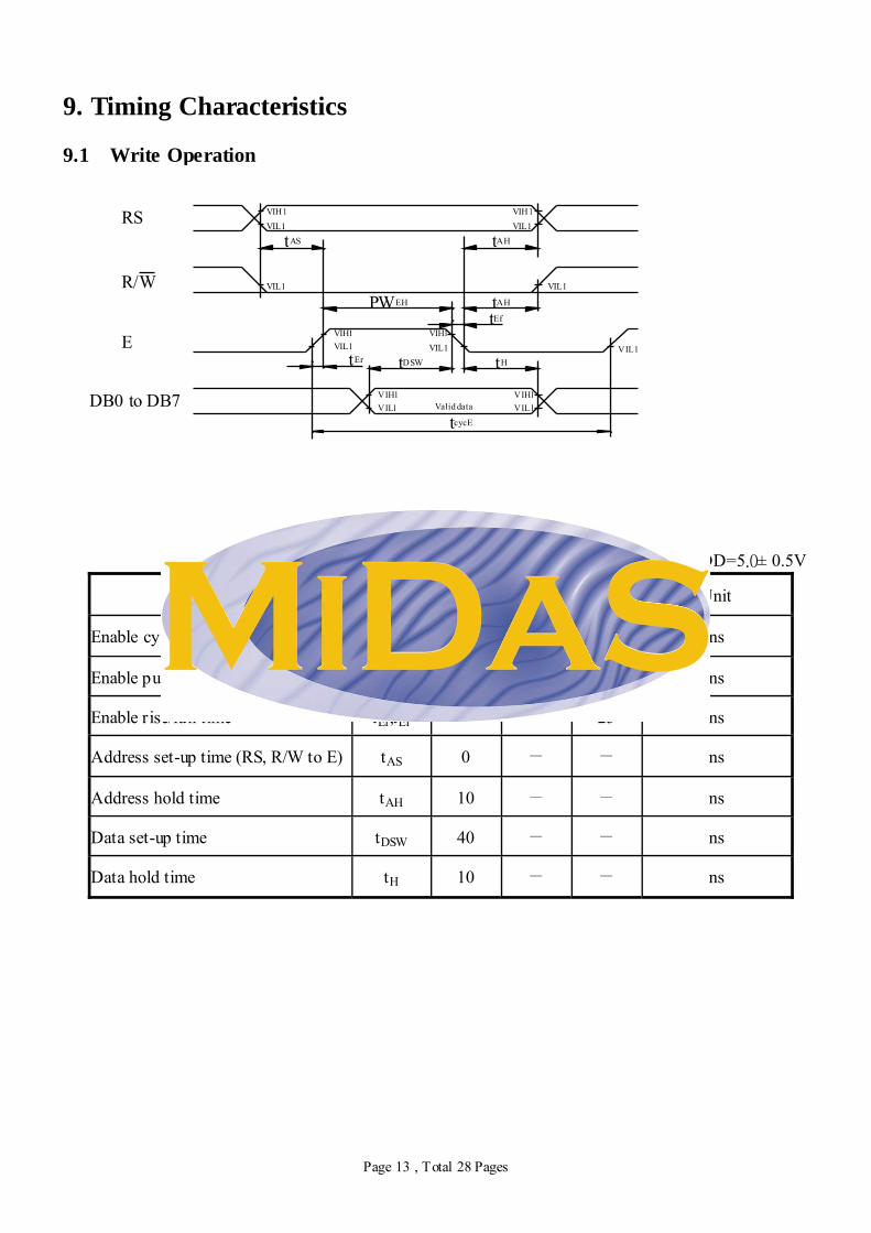
The LCD display Module is built in a LSI controller, the controller has two 8-bit registers, an instruction register (IR) and a data register (DR). The IR stores instruction codes, such as display clear and cursor shift, and address information for display data RAM (DDRAM) and character generator (CGRAM). The IR can only be written from the MPU. The DR temporarily stores data to be written or read from DDRAM or CGRAM. When address information is written into the IR, then data is stored into the DR from DDRAM or CGRAM. By the register selector (RS) signal, these two registers can be selected. RS R/W Operation
0 0 IR write as an internal operation (display clear, etc.)
0 1 Read busy flag (DB7) and address counter (DB0 to DB7)
1 0 Write data to DDRAM or CGRAM (DR to DDRAM or CGRAM)
1 1 Read data from DDRAM or CGRAM (DDRAM or CGRAM to DR)
Busy Flag (BF)
When the busy flag is 1, the controller LSI is in the internal operation mode, and the next instruction will not be accepted. When RS=0 and R/W=1, the busy flag is output to DB7. The next instruction must be written after ensuring that the busy flag is 0.
Address Counter (AC) The address counter (AC) assigns addresses to both DDRAM and CGRAM. Display Data RAM (DDRAM) This DDRAM is used to store the display data represented in 8-bit character codes. Its extended capacity is 80×8 bits or 80 characters. Below figure is the relationships between DDRAM addresses and positions on the liquid crystal display.
AC (hexadecimal)
High bits Low bits
AC6 AC5 AC4 AC3 AC2 AC1 AC0 1 0 0 1 1 1 0
Example: DDRAM addresses 4E
Page 9 , Total 28 Pages
Character Generator ROM (CGROM) The CGROM generate 5×8 dot or 5×10 dot character patterns from 8-bit character codes. See Table 2.
Character Generator RAM (CGRAM) In CGRAM, the user can rewrite character by program. For 5×8 dots, eight character patterns can be
written, and for 5×10 dots, four character patterns can be written. Write into DDRAM the character code at the addresses shown as the left column of table 1. To show the character patterns stored in CGRAM.
F o r 5 * 1 0 d o t c h a r a c t e r p a tte r n sC h a r a c te r C o d e s( D D R A M d a ta ) C G R A M A d d r e s s C h a r a c te r P a tte r n s
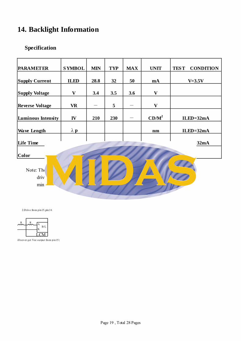
Note: The LED of B/L is drive by current only, drive voltage is for reference only. drive voltage can make driving current under safety area (current between minimum and maximum).
ill never get Vee output from pin15)
LCM
R
2.D rive from pin15,pin16
R A
KB/L
Page 20 , Total 28 Pages
15. Reliability Content of Reliability Test (wide temperature, -20~70)
Note1: No dew condensation to be observed. Note2: The function test shall be conducted after 4 hours storage at the normal Temperature and humidity after remove from the test chamber. Note3: Vibration test will be conducted to the product itself without putting it in a container.
Environmental Test
Test Item Content of Test Test Condition Note
High Temperature storage Endurance test applying the high storage temperature for a long
time.
80
200hrs 2
Low Temperature storage
Endurance test applying the high storage temperature for a long time.
-30 200hrs
1,2
High Temperature Operation
Endurance test applying the electric stress (Voltage & Current) and the thermal stress to the element for a long time.
70 200hrs
——
Low Temperature
Operation
Endurance test applying the electric stress under low temperature
for a long time.
-20
200hrs 1
High Temperature/
Humidity Operation
The module should be allowed to stand at 60 ,90%RH max
For 96hrs under no-load condition excluding the polarizer, Then taking it out and drying it at normal temperature.
60 ,90%RH
96hrs 1,2
Thermal shock resistance
The sample should be allowed stand the following 10 cycles of operation
-20 25 70
30min 5min 30min
1 cycle
-20 / 70 10 cycles
——
Vibration test Endurance test applying the vibration during transportation and using.
Total fixed amplitude : 15mm
Vibration Frequency : 10~55Hz
One cycle 60 seconds to 3 directions of X,Y,Z for
Each 15 minutes
3
Static electricity test Endurance test applying the electric stress to the terminal.
VS=800V,RS=1.5kΩ
CS=100pF 1 time
——
Page 21 , Total 28 Pages
16. Inspection specification
NO Item Criterion AQL
01 Electrical Testing
1.1 Missing vertical, horizontal segment, segment contrast defect. 1.2 Missing character , dot or icon. 1.3 Display malfunction. 1.4 No function or no display. 1.5 Current consumption exceeds product specifications. 1.6 LCD viewing angle defect. 1.7 Mixed product types. 1.8 Contrast defect.
0.65
02 Black or white spots on LCD (display only)
2.1 White and black spots on display ≦0.25mm, no more than
three white or black spots present. 2.2 Densely spaced: No more than two spots or lines within 3mm
2.5
3.1 Round type : As following drawing
Φ=( x + y ) / 2
SIZE Acceptable Q TY
Φ≦0.10 Accept no dense 0.10<Φ≦0.20 2 0.20<Φ≦0.25 1 0.25<Φ 0
2.5
03
LCD black spots, white
spots, contamination (non-display) 3.2 Line type : (As following drawing)
Length Width Acceptable Q TY --- W≦0.02 Accept no dense
L≦3.0 0.02<W≦0.03 L≦2.5 0.03<W≦0.05
2
--- 0.05<W As round type
2.5
04 Polarizer bubbles
If bubbles are visible, judge using black spot specifications, not easy to find, must check in specify direction.
Size Φ Acceptable Q TY Φ≦0.20 Accept no dense
0.20<Φ≦0.50 3 0.50<Φ≦1.00 2 1.00<Φ 0
Total Q TY 3
2.5
Page 22 , Total 28 Pages
NO Item Criterion AQL 05 Scratches Follow NO.3 LCD black spots, white spots, contamination
06 Chipped glass
Symbols Define: x: Chip length y: Chip width z: Chip thickness k: Seal width t: Glass thickness a: LCD side length L: Electrode pad length: 6.1 General glass chip : 6.1.1 Chip on panel surface and crack between panels:
z: Chip thickness y: Chip width x: Chip length Z≦1/2t Not over viewing
area x≦1/8a
1/2t<z≦2t Not exceed 1/3k x≦1/8a If there are 2 or more chips, x is total length of each chip. 6.1.2 Corner crack:
z: Chip thickness y: Chip width x: Chip length Z≦1/2t Not over viewing
area x≦1/8a
1/2t<z≦2t Not exceed 1/3k x≦1/8a If there are 2 or more chips, x is the total length of each chip.
2.5
Page 23 , Total 28 Pages
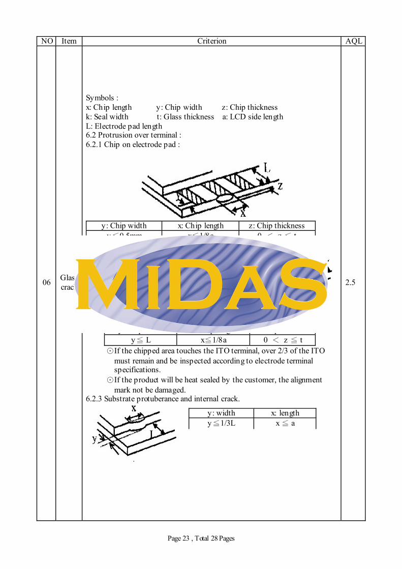
NO Item Criterion AQL
06 Glass crack
Symbols : x: Chip length y: Chip width z: Chip thickness k: Seal width t: Glass thickness a: LCD side length L: Electrode pad length 6.2 Protrusion over terminal : 6.2.1 Chip on electrode pad :
y: Chip width x: Chip length z: Chip thickness
y≦0.5mm x≦1/8a 0 < z ≦ t 6.2.2 Non-conductive portion:
y: Chip width x: Chip length z: Chip thickness
y≦ L x≦1/8a 0 < z ≦ t If the chipped area touches the ITO terminal, over 2/3 of the ITO
must remain and be inspected according to electrode terminal specifications.
If the product will be heat sealed by the customer, the alignment mark not be damaged.
6.2.3 Substrate protuberance and internal crack.
y: width x: length y≦1/3L x ≦ a
2.5
Page 24 , Total 28 Pages
NO Item Criterion AQL
07 Cracked glass The LCD with extensive crack is not acceptable. 2.5
08 Backlight elements
8.1 Illumination source flickers when lit. 8.2 Spots or scratched that appear when lit must be judged. Using
LCD spot, lines and contamination standards. 8.3 Backlight doesn’t light or color wrong.
0.65 2.5 0.65
09 Bezel
9.1 Bezel may not have rust, be deformed or have fingerprints,
stains or other contamination. 9.2 Bezel must comply with job specifications.
2.5 0.65
10 PCB、COB
10.1 COB seal may not have pinholes larger than 0.2mm or
contamination. 10.2 COB seal surface may not have pinholes through to the IC. 10.3 The height of the COB should not exceed the height indicated
in the assembly diagram. 10.4 There may not be more than 2mm of sealant outside the seal
area on the PCB. And there should be no more than three places.
10.5 No oxidation or contamination PCB terminals. 10.6 Parts on PCB must be the same as on the production
characteristic chart. There should be no wrong parts, missing parts or excess parts.
10.7 The jumper on the PCB should conform to the product characteristic chart.
10.8 If solder gets on bezel tab pads, LED pad, zebra pad or screw hold pad, make sure it is smoothed down.
10.9 The Scraping testing standard for Copper Coating of PCB
YX
X * Y<=2mm2
2.5 2.5 0.65 2.5 2.5 0.65 0.65 2.5 2.5
11 Soldering
11.1 No un-melted solder paste may be present on the PCB. 11.2 No cold solder joints, missing solder connections, oxidation
or icicle. 11.3 No residue or solder balls on PCB. 11.4 No short circuits in components on PCB.
2.5 2.5 2.5 0.65
Page 25 , Total 28 Pages
NO Item Criterion AQL
12 General appearance
12.1 No oxidation, contamination, curves or, bends on interface
Pin (OLB) of TCP. 12.2 No cracks on interface pin (OLB) of TCP. 12.3 No contamination, solder residue or solder balls on product. 12.4 The IC on the TCP may not be damaged, circuits. 12.5 The uppermost edge of the protective strip on the interface
pin must be present or look as if it cause the interface pin to sever.
12.6 The residual rosin or tin oil of soldering (component or chip component) is not burned into brown or black color.
12.7 Sealant on top of the ITO circuit has not hardened. 12.8 Pin type must match type in specification sheet. 12.9 LCD pin loose or missing pins. 12.10 Product packaging must the same as specified on packaging
specification sheet. 12.11 Product dimension and structure must conform to product
specification sheet.
2.5 0.65 2.5 2.5 2.5 2.5 2.5 0.65 0.65 0.65 0.65
17. Precautions in use of LCD Modules
(1)Avoid applying excessive shocks to the module or making any alterations or modifications to it. (2)Don’t make extra holes on the printed circuit board, modify its shape or change the components of
LCD module. (3)Don’t disassemble the LCM. (4)Don’t operate it above the absolute maximum rating. (5)Don’t drop, bend or twist LCM. (6)Soldering: only to the I/O terminals. (7)Storage: please storage in anti-static electricity container and clean environment.
Page 26 , Total 28 Pages
18. Material List of Components for RoHs 1. Midas Components Ltd. hereby declares that all of or part of products, including, but not limited to, the
LCM, accessories or packages, manufactured and/or delivered to your company (including your subsidiaries
and affiliated company) directly or indirectly by our company (including our subsidiaries or affil iated companies)
do not intentionally contain any of the substances listed in all applicable EU directives and regulations,
including the following substances.
Exhibit A:The Harmful Material List
Material (Cd) (Pb) (Hg) (Cr6+) PBBs PBDEs
Limited
Value
100
ppm
1000
ppm
1000
ppm
1000
ppm
1000
ppm
1000
ppm
Above limited value is set up according to RoHS. 2.Process for RoHS requirement:
(1) Use the Sn/Ag/Cu soldering surface;the surface of Pb-free solder is rougher than we used before.
(2) Heat-resistance temp.: Reflow:250 ,30 seconds Max. ; Connector soldering wave or hand soldering:320 , 10 seconds max.
(3) Temp. curve of reflow, max. Temp.:235±5; Recommended customer’s soldering temp. of connector:280 , 3 seconds.