29
Advanced Digital Circuits ECET 146 Week 4 Professor Iskandar Hack ET 221G, 481-5733 [email protected]
| Date post: | 31-Dec-2015 |
| Category: |
Documents |
| Upload: | winfred-hicks |
| View: | 215 times |
| Download: | 2 times |

Advanced Digital CircuitsECET 146
Week 4
Professor Iskandar Hack
ET 221G, 481-5733

This Week’s Goals
Introduction to AHDL Designing a Combinational Circuit from a
Truth Table using the Table Command in AHDL

Design ExampleA B C D X
0 0 0 0 0
0 0 0 1 0
0 0 1 0 1
0 0 1 1 1
0 1 0 0 1
0 1 0 1 0
0 1 1 0 0
0 1 1 1 1
1 0 0 0 1
1 0 0 1 0
1 0 1 0 0
1 0 1 1 1
1 1 0 0 1
1 1 0 1 0
1 1 1 0 1
1 1 1 1 0

Introduction AHDL
Altera Hardware Design Language (AHDL) is a way of designing digital circuits by defining in a text format the functionality of the circuit.
AHDL is NOT a programming language!!! AHDL is a concurrent language. All behavior
specified in the Logic Section of a TDF is evaluated at the same time rather than sequentially.
All AHDL instructions are translated into hardware, and as such commands such as a=a+1 are not supported.

AHDL File Format – Subdesign Spec
The top part of the file contains the subdesign I/O specification. It has the name of the design followed by all of the I/O pins.
Important note – the name of the subdesign (lab4b in this case) must be the same name as the file. This file must be named lab4b.tdf
Do not use X as a node name – it is reserved in AHDL

AHDL File Format – Logic Section
After the subdesign section you can name any internal nodes (not shown in this lab)
After the naming internal nodes then the logic section follows denoted with a Begin and End
Logic

AHDL Complete File

The Table Keyword
A table is the easiest way to implement combinational logic in AHDL, you simply enter the truth table as you want it.
The Table begins with the keyword TABLE Followed by a line that specifies the inputs
and outputs for the table (note you can implement as many outputs as you want)
The inputs and outputs are then entered in the table in the syntax shown (next slide)
The table ends with the keyword END TABLE

Completed Table
Inputs in Hex format
Values from Truth Table
Start of Table
Inputs and Outputs of Table
End of Table

Implementing a Design in AHDL
Select New -> AHDL Design File
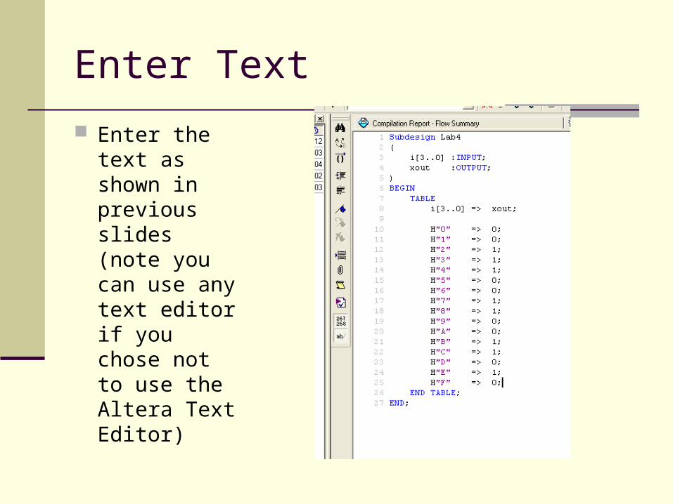
Enter Text
Enter the text as shown in previous slides (note you can use any text editor if you chose not to use the Altera Text Editor)

Save File
Note – SeparateDirectory with sameName as File
Ext .tdf
Create Project as before
NOTE: The name of the project MUST be the same as the Subdesign name on the previousslide.

Compile and Simulate Steps (refer to earlier slides for details) Create Project Specify Part Don’t set pins yet (the system doesn’t know what
your I/O pins are until the first compile, you’ll get a warning)
Also note that this time I named the pins i0, i1, i2, i3 Compile the project Assign the pins as before Recompile the project Create Waveform Vector Files (see previous labs) Simulate the design

Simulation

Connect the Altera Board to the PC
Check out an Altera Board from the Lab Tech office
DO NOT connect any parts to the board before programming!!!!
The board has the design from the last time it was used and it’s possible that some inputs now are now outputs and that you can destroy the part.

Connect Board to PC I
When checking out board also check out DC wall pack. Ensure that the wall pack is of the correct polarity (+ is the center, - is the outside) and is between 9 and 12 volts.
Also get a Male -> Female DB25 cable to connect between the computer and the PC

Connect to PC II
Notice the location of the connectors used, the other DB25 connector is used for experiments.
DB25 Cable to PC DC Power connector

Open the Programming Module
Select the Programmer Hot Button

Select Programming Hardware
Once the programmer is opened – hit hardware setup
Then select Add Hardware
Selected Byteblaster on LPT1:

Select Programming Options
Select Program/Configure and Verify

Program the Part
Hit the start button You should see the
progress bar move and the red LED come on (on the board) during programming

Wire up Board
Connect VCC and Ground to the proto board by using the +5 volts and Ground on the top of the board.
DO NOT use the unregulated DC!!! This could be as high as +12 volts and will destroy the part.
Place wires from the Input's to Ground on the proto board (this is input A=0, B=0, C=0, D=0)

Wire Up Board II
For this Lab we’ll use positive logic (the Altera part supplies the 5 volts for the LED), so connect the LED as shown.

Wired Board
Your board after wiring should resemble the following:
Inputs
Output X

Wire up Board
Connect VCC and Ground to the proto board by using the +5 volts and Ground on the top of the board.
DO NOT use the unregulated DC!!! This could be as high as +12 volts and will destroy the part.
Place wires from the Input's to Ground on the proto board (this is input A=0, B=0, C=0, D=0)

Wire Up Board II
For this Lab we’ll use positive logic (the Altera part supplies the 5 volts for the LED), so connect the LED as shown.

Verify the Design
Move the input wires thru the 16 possible combinations (0000 to 1111) to verify that the design matches the truth table

Summary
This week we covered how to design a circuit without drawing ANY schematics using the waveform editor
We also got our first look at designing a circuit by using AHDL (also without drawing schematics)
We also we reviewed how to verify a combinational logic design using the Altera hardware

Lab Three
Design a circuit and verify it using the techniques (first using waveform design and again using AHDL) covered in this week’s lecture that will have the following truth table.
Turn in your printouts from the schematic editor and simulator.
Download only the project from AHDL to the board and verify it’s operation in hardware
A B C D X
0 0 0 0 1
0 0 0 1 1
0 0 1 0 0
0 0 1 1 0
0 1 0 0 1
0 1 0 1 0
0 1 1 0 0
0 1 1 1 0
1 0 0 0 0
1 0 0 1 0
1 0 1 0 0
1 0 1 1 0
1 1 0 0 0
1 1 0 1 0
1 1 1 0 1
1 1 1 1 1


