Page 1
STANFORD
Advanced LIGO Photodiode Development
______
David Jackrel, PhD Candidate
Stanford University
Dept. of Materials Science and Engineering
James S. Harris
Hannover, Germany
August 20th, 2003
LIGO-G030495-00-Z
Page 2
STANFORD
Outline
Motivation & Introduction AdLIGO PD Specifications Device Materials and Design
InGaAs vs. GaInNAs
Device Results Thinned Device QE InGaAs & GaInNAs I-V 2m Thick GaInNAs Absorption
Predictions
Page 3
STANFORD
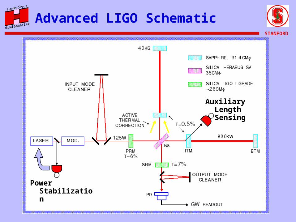
Advanced LIGO Schematic
Power Stabilization
Auxiliary Length Sensing
Page 4
STANFORD
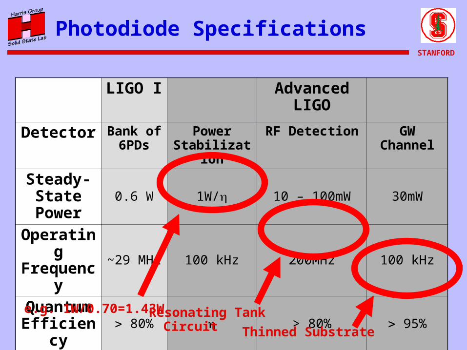
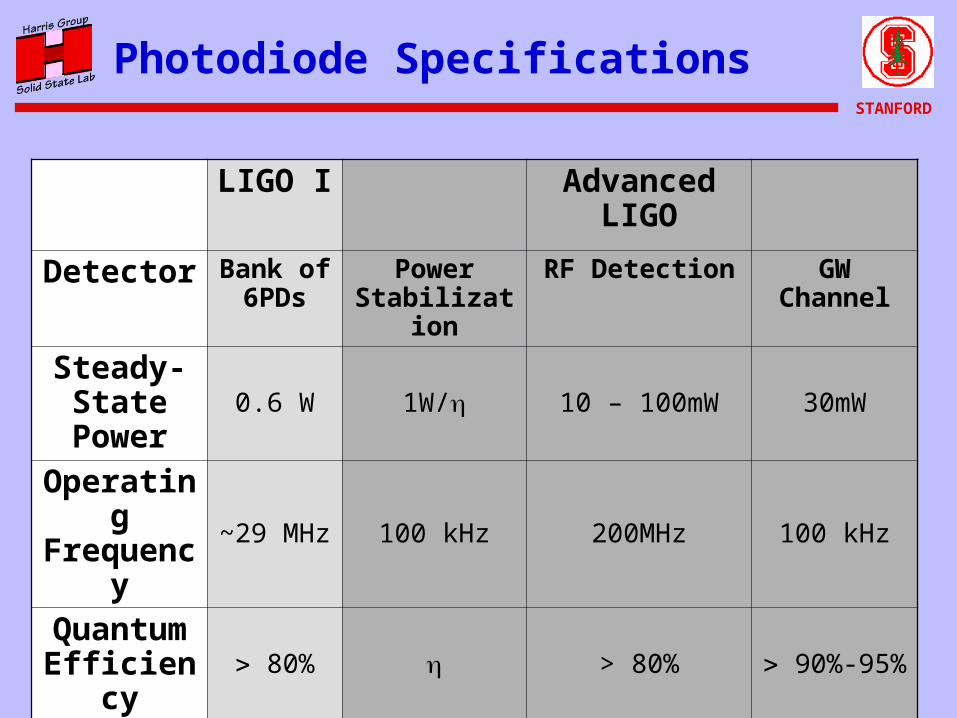
Photodiode Specifications
LIGO I Advanced LIGO
Detector
Bank of 6PDs
Power Stabilizati
on
RF Detection GW Channel
Steady-State Power
0.6 W 1W/ 10 – 100mW 30mW
Operating
Frequency
~29 MHz 100 kHz 200MHz 100 kHz
Quantum
Efficiency
80% > 80% 95%
e.g. 1W/0.70=1.43W
Resonating Tank Circuit Thinned Substrate
Page 5
STANFORD
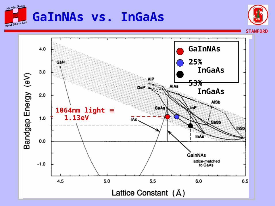
GaInNAs vs. InGaAs
GaInNAs
25% InGaAs
53% InGaAs
1064nm light 1.13eV
Page 6
STANFORD
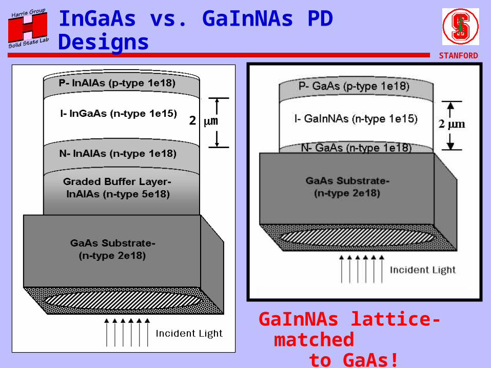
InGaAs vs. GaInNAs PD Designs
2 m
GaInNAs lattice-matched to
GaAs!
Page 7
STANFORD
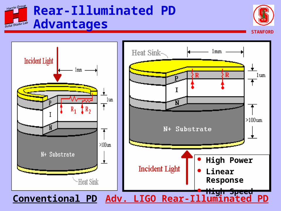
Rear-Illuminated PD Advantages
Conventional PD Adv. LIGO Rear-Illuminated PD
High Power Linear
Response High Speed
Page 8
STANFORD
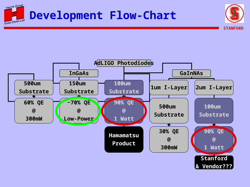
Development Flow-Chart
AdLIGO Photodiodes
InGaAs GaInNAs
500um
Substrate
150um
Substrate1um I-Layer 2um I-Layer
100um
Substrate
100um
Substrate
90% QE
@
1 Watt
90% QE
@
1 Watt
~70% QE
@
Low-Power
60% QE
@
300mW
500um
Substrate
Stanford
& Vendor???
Hamamatsu
Product
30% QE
@
300mW
Page 9
STANFORD
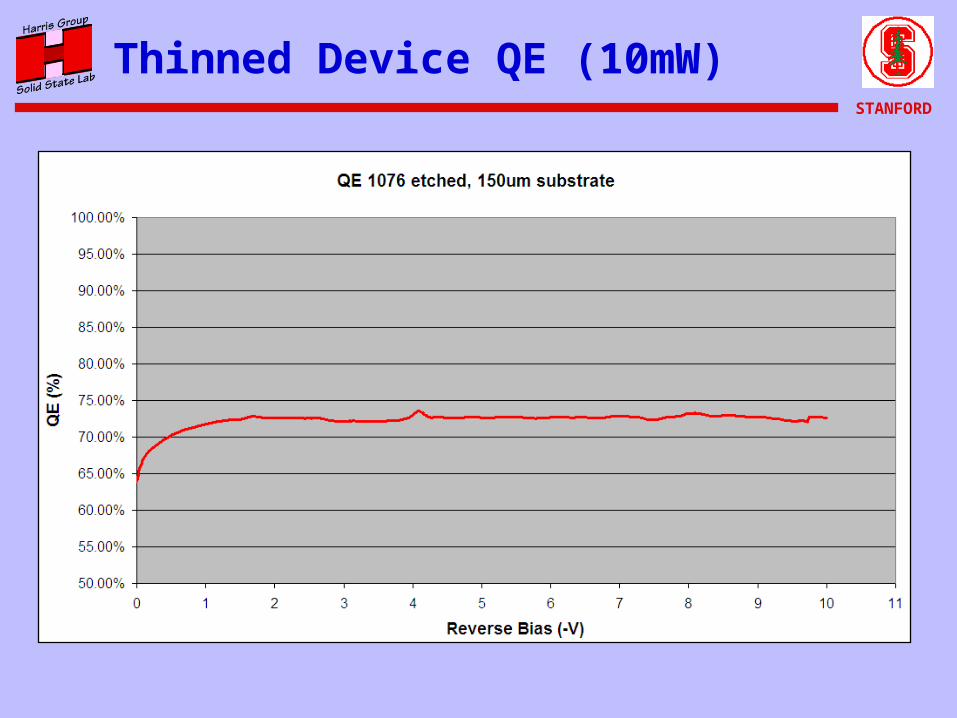
Thinned Device QE (10mW)
Page 10
STANFORD
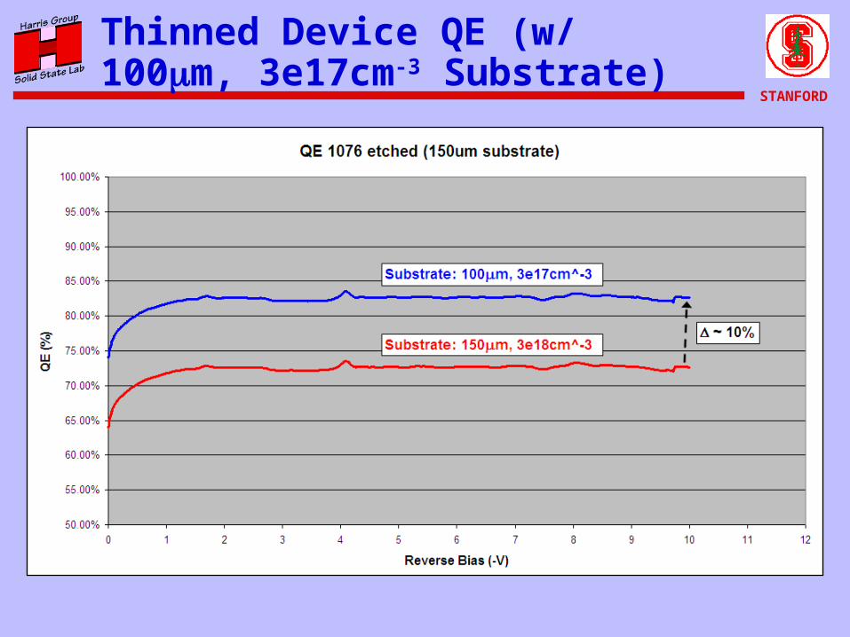
Thinned Device QE (w/ 100m, 3e17cm-3 Substrate)
Page 11
STANFORD
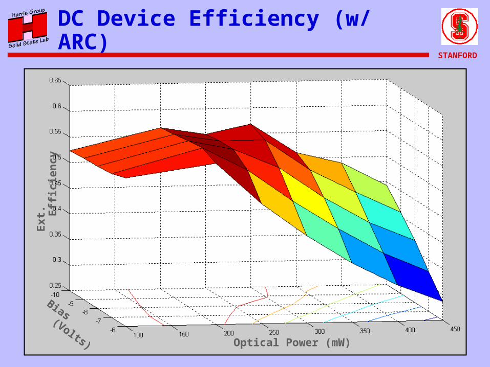
DC Device Efficiency (w/ ARC)E
xt.
Eff
icie
ncy
Optical Power (mW)
Bias (Volts)
Page 12
STANFORD
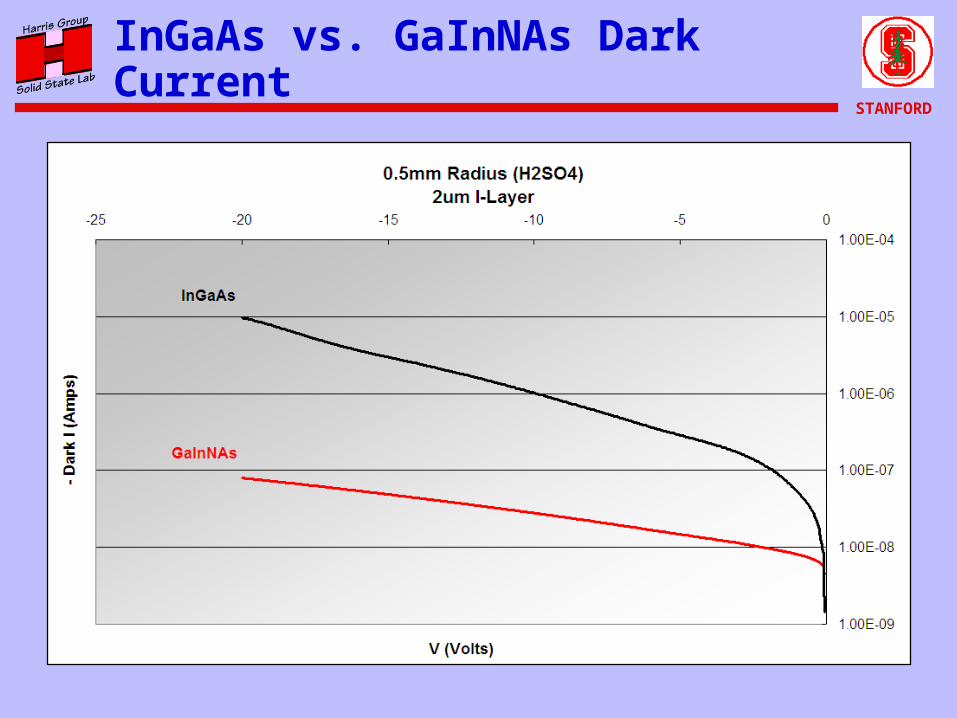
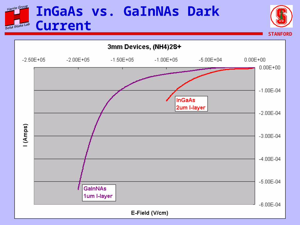
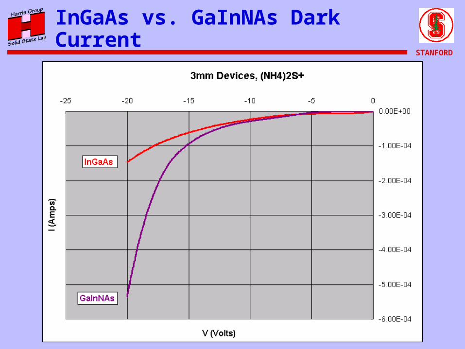
InGaAs vs. GaInNAs Dark Current
Page 13
STANFORD
InGaAs vs. GaInNAs Dark Current
Page 14
STANFORD
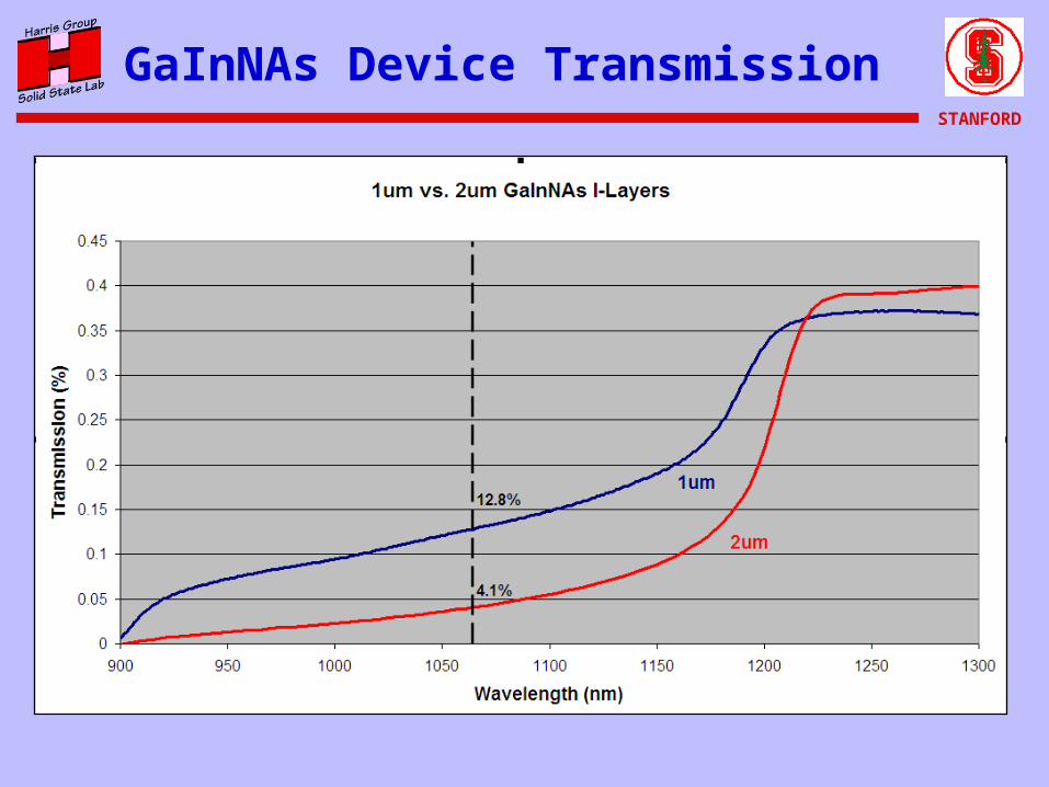
GaInNAs Device Transmission
Page 15
STANFORD
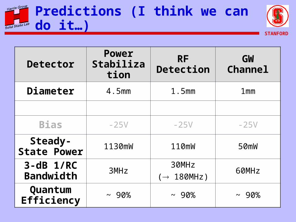
Predictions (I think we can do it…)
DetectorPower
Stabilization
RF Detection
GW Channel
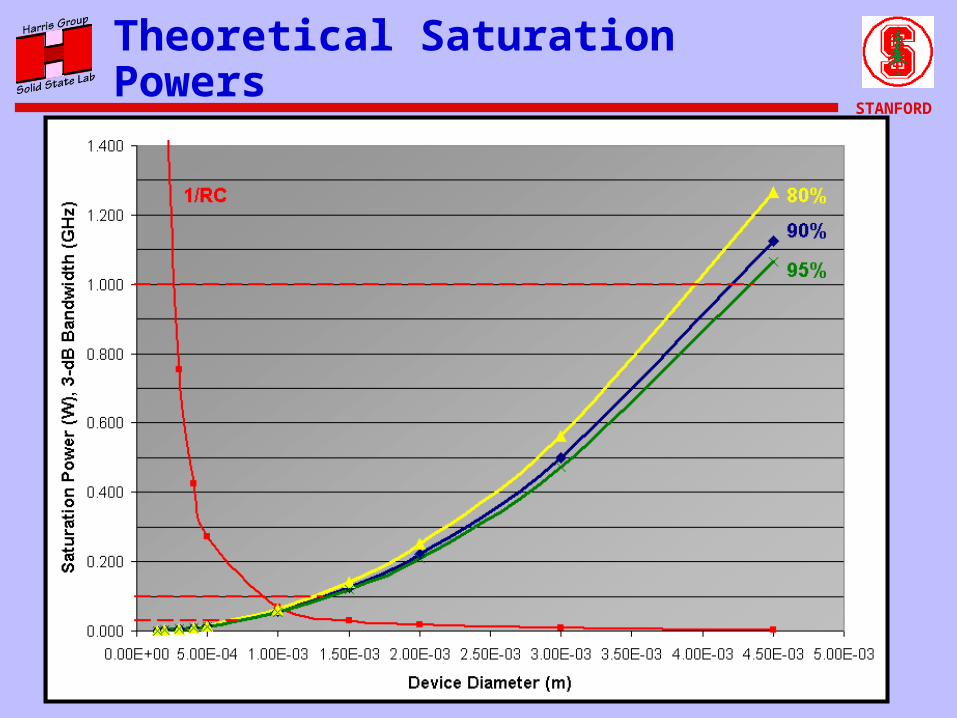
Diameter 4.5mm 1.5mm 1mm
Bias -25V -25V -25V
Steady-State Power
1130mW 110mW 50mW
3-dB 1/RC Bandwidth
3MHz30MHz
( 180MHz)60MHz
Quantum Efficiency
~ 90% ~ 90% ~ 90%
Page 16
STANFORD
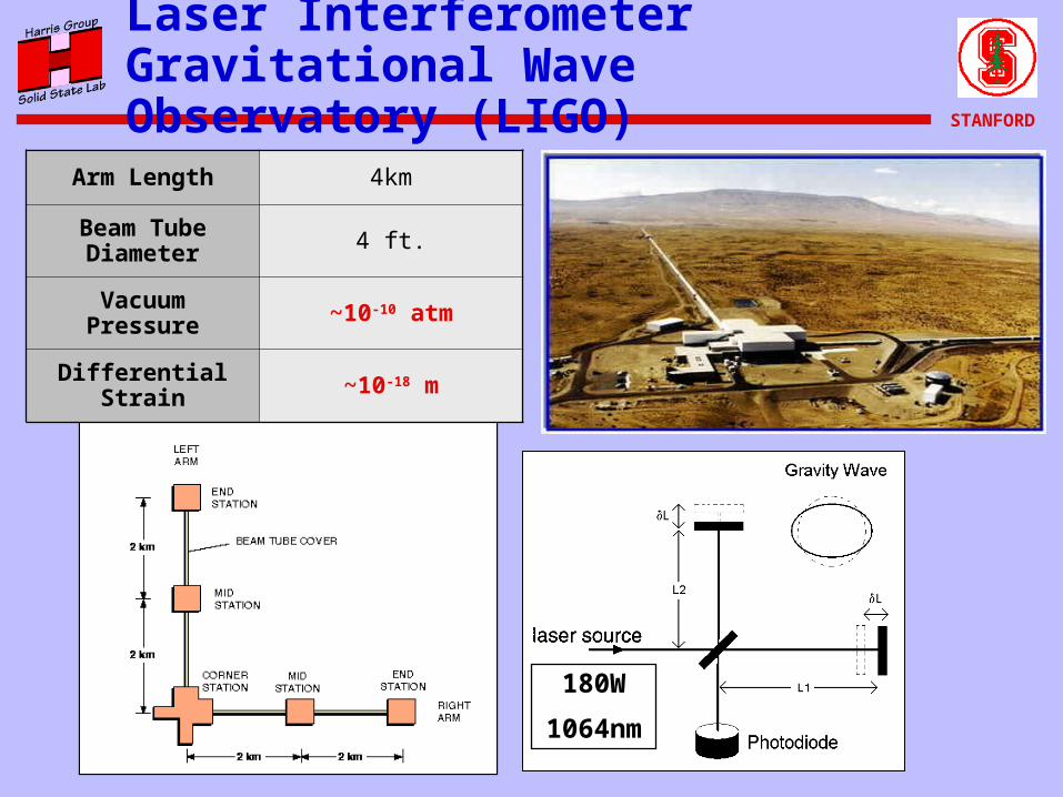
Laser Interferometer Gravitational Wave Observatory (LIGO)
Arm Length 4km
Beam Tube Diameter 4 ft.
Vacuum Pressure ~10-10 atm
Differential Strain ~10-18 m
180W
1064nm
Page 17
STANFORD
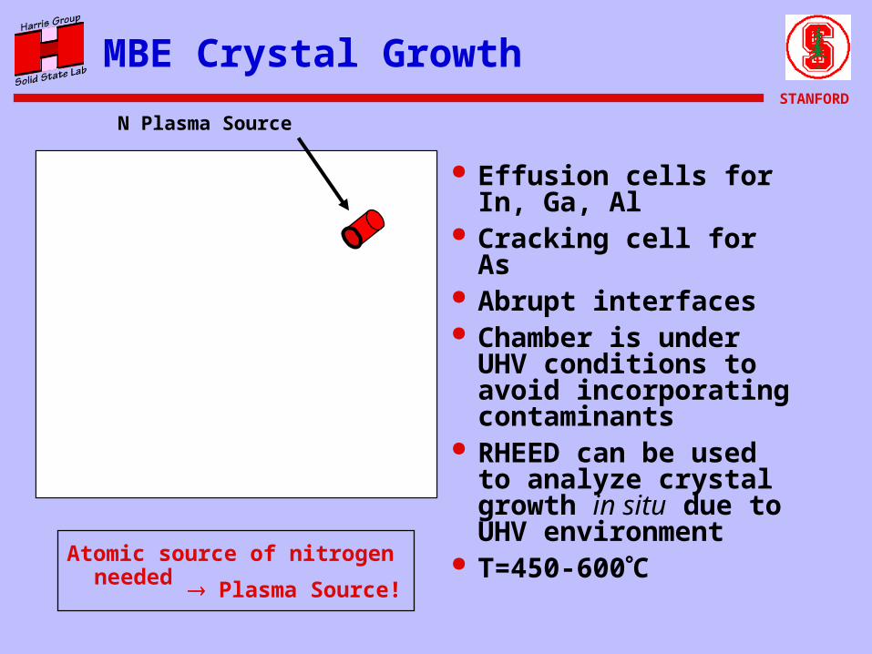
MBE Crystal Growth
Effusion cells for In, Ga, Al
Cracking cell for As Abrupt interfaces Chamber is under
UHV conditions to avoid incorporating contaminants
RHEED can be used to analyze crystal growth in situ due to UHV environment
T=450-600C
N Plasma Source
Atomic source of nitrogen needed Plasma Source!
Page 18
STANFORD
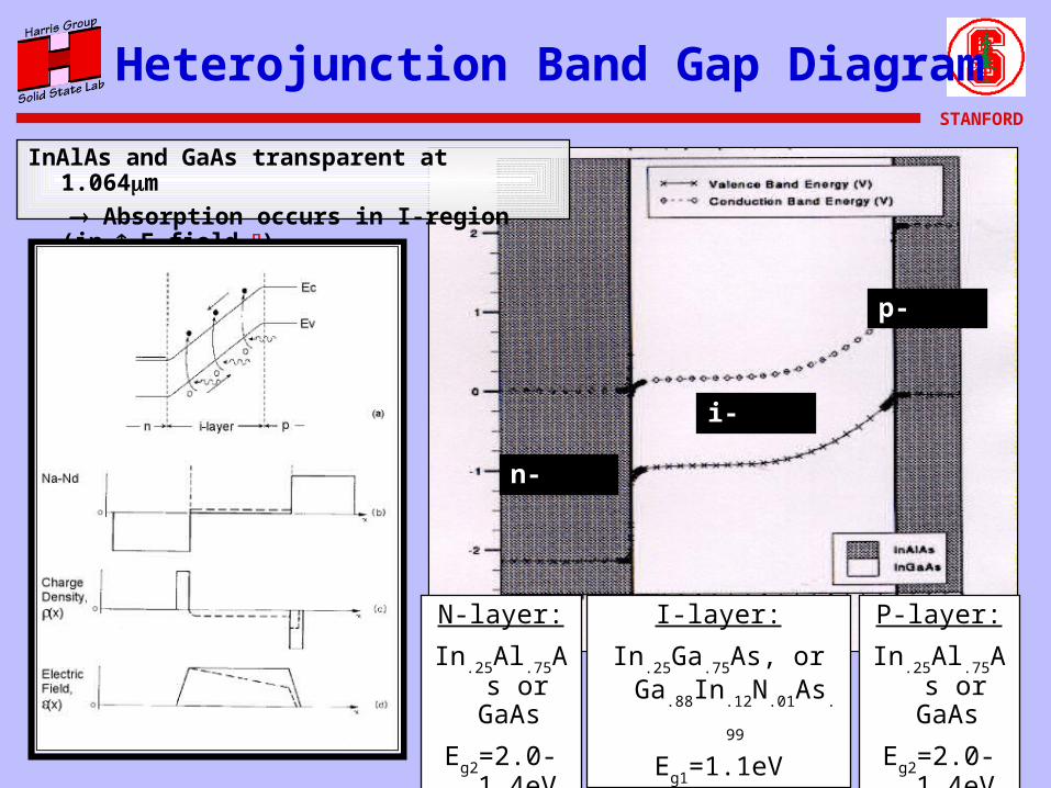
Heterojunction Band Gap Diagram
N-layer:
In.25Al.75As or GaAs
Eg2=2.0-1.4eV
P-layer:
In.25Al.75As or GaAs
Eg2=2.0-1.4eV
I-layer:
In.25Ga.75As, or Ga.88In.12N.01As.99
Eg1=1.1eV
n-
i-
p-
InAlAs and GaAs transparent at 1.064m
Absorption occurs in I-region (in E-field )
Page 19
STANFORD
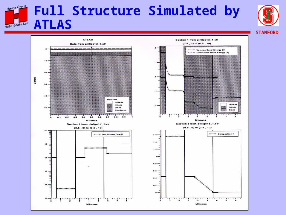
Full Structure Simulated by ATLAS
Page 20
STANFORD
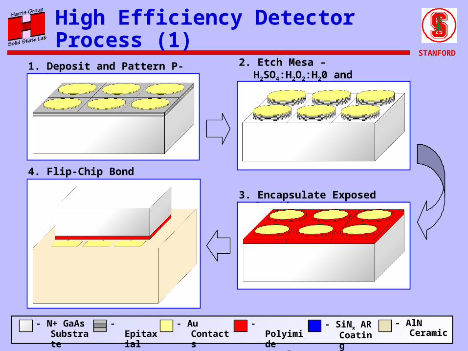
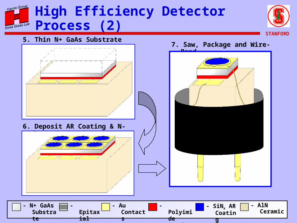
High Efficiency Detector Process (1)
1. Deposit and Pattern P-Contact
2. Etch Mesa – H2SO4:H2O2:H20 and Passivate in (NH4)2S+
3. Encapsulate Exposed Junction
4. Flip-Chip Bond
- N+ GaAs Substrate
- Epitaxial Layers
- Au Contacts
- Polyimide Insulator
- SiNx AR Coating
- AlN Ceramic
Page 21
STANFORD
High Efficiency Detector Process (2)
6. Deposit AR Coating & N-Contact
7. Saw, Package and Wire-Bond
- N+ GaAs Substrate
- Epitaxial Layers
- Au Contacts
- Polyimide Insulator
- SiNx AR Coating
- AlN Ceramic
5. Thin N+ GaAs Substrate
Page 22
STANFORD
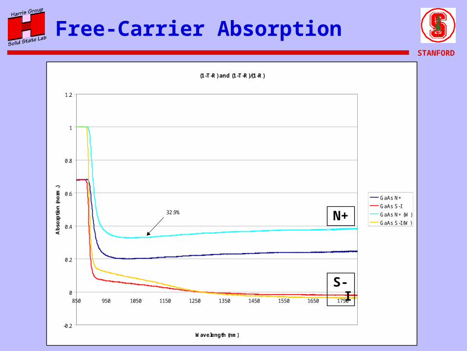
Free-Carrier Absorption
(1-T-R) and (1-T-R)/(1-R)
-0.2
0
0.2
0.4
0.6
0.8
1
1.2
850 950 1050 1150 1250 1350 1450 1550 1650 1750
Wavelength (nm)
Ab
sorp
tio
n (
no
rm.)
GaAs N+
GaAs S-I
GaAs N+ (W)
GaAs S-I (W)
32.9% N+
S-I
Page 23
STANFORD
Free-Carrier Absorption
Page 24
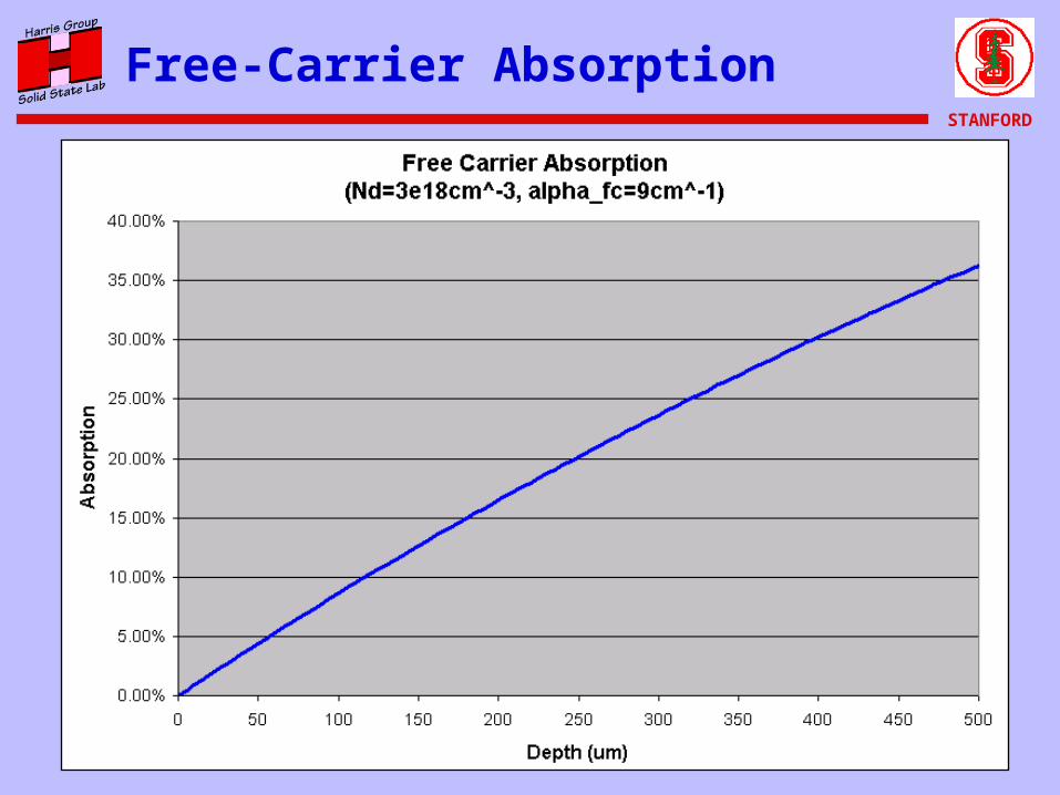
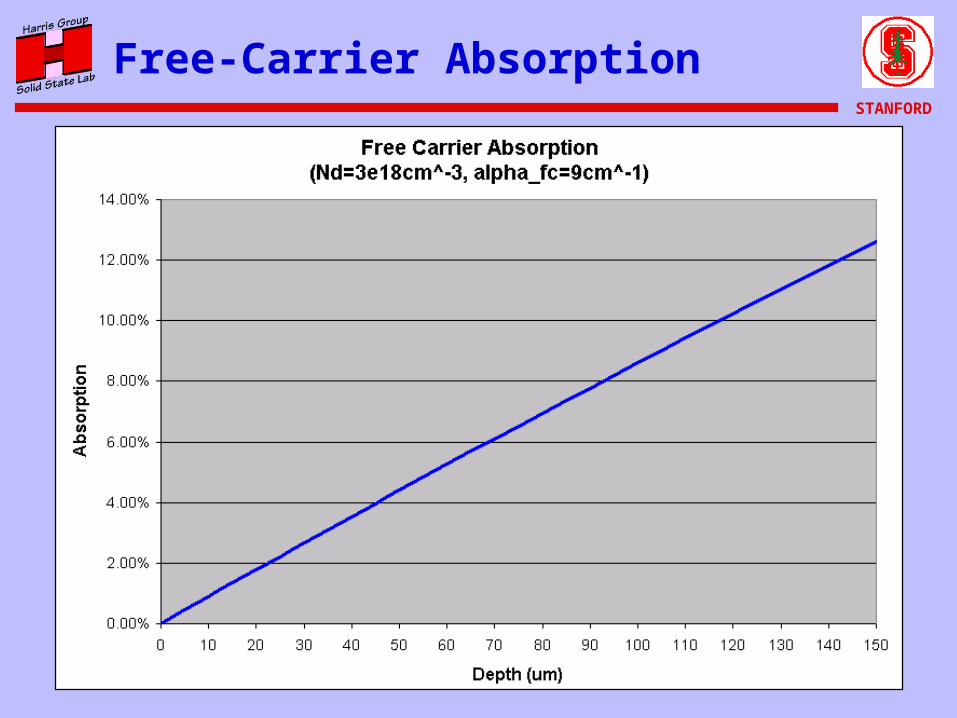
STANFORD
Free-Carrier Absorption
Page 25
STANFORD
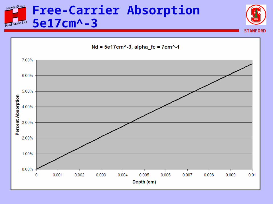
Free-Carrier Absorption 5e17cm^-3
Page 26
STANFORD
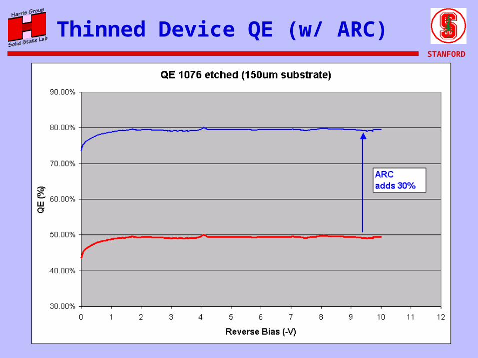
Thinned Device QE (w/ ARC)
Page 27
STANFORD
Photodiode Specifications
LIGO I Advanced LIGO
Detector
Bank of 6PDs
Power Stabilizati
on
RF Detection GW Channel
Steady-State Power
0.6 W 1W/ 10 – 100mW 30mW
Operating
Frequency
~29 MHz 100 kHz 200MHz 100 kHz
Quantum
Efficiency
80% > 80% 90%-95%
Page 28
STANFORD
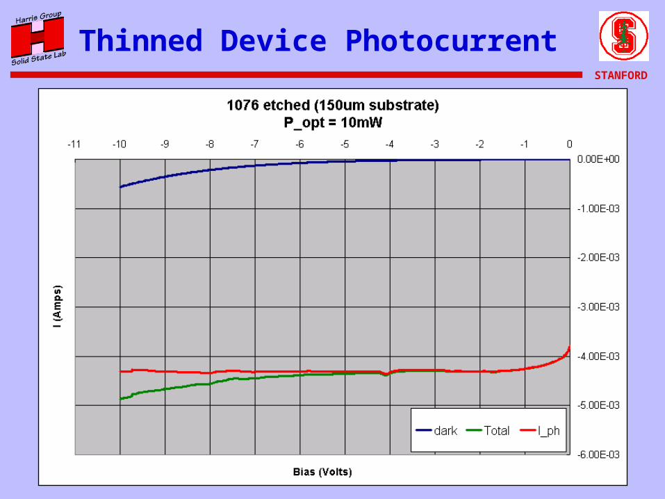
Thinned Device Photocurrent
Page 29
STANFORD
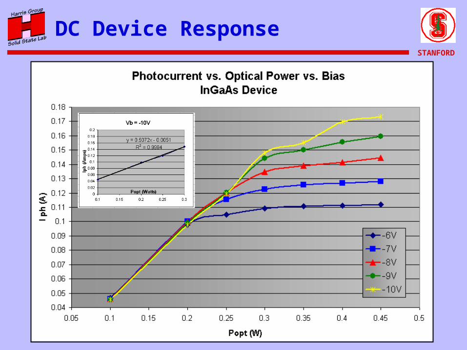
DC Device Response
Page 30
STANFORD
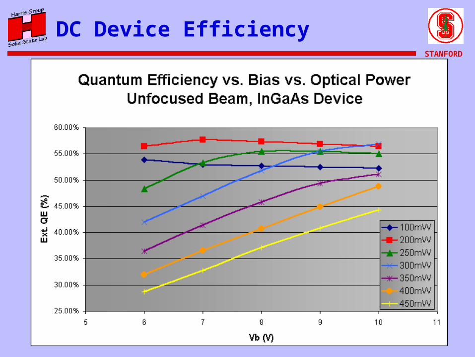
DC Device Efficiency
Page 31
STANFORD
Free-Carrier Absorption
A = 1 – exp(-tsub•fc) , fc = Nd * 3e-18
Page 32
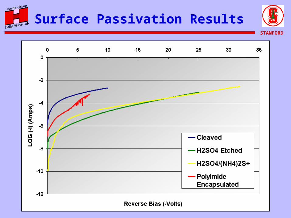
STANFORD
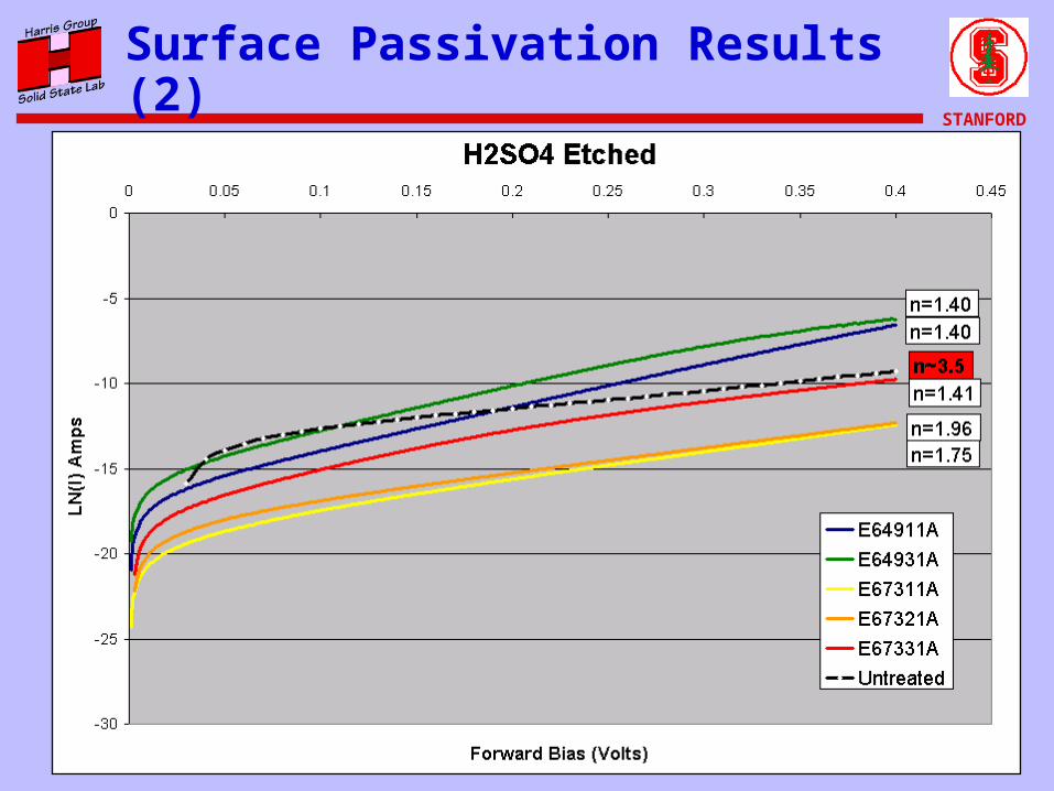
Surface Passivation Results (2)
Page 33
STANFORD
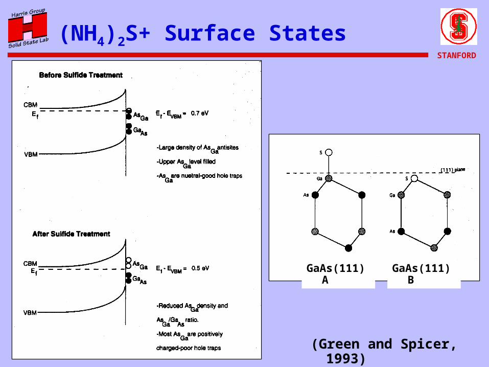
(NH4)2S+ Surface States
(Green and Spicer, 1993)
GaAs(111)A GaAs(111)B
Page 34
STANFORD
Surface Passivation Results
Page 35
STANFORD
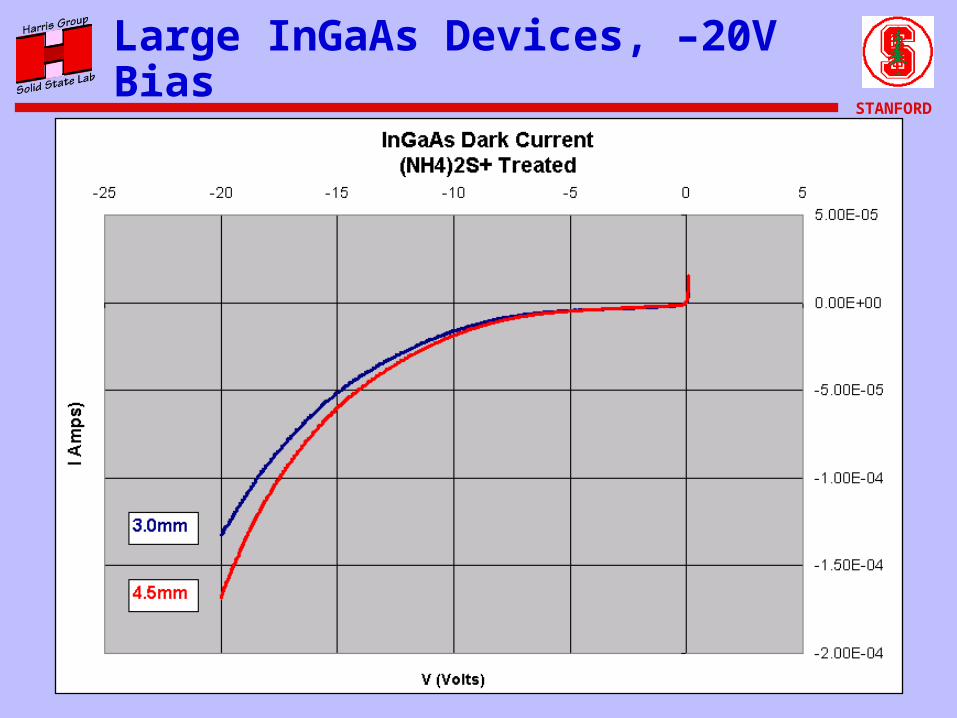
Large InGaAs Devices, –20V Bias
Page 36
STANFORD
InGaAs vs. GaInNAs Dark Current
Page 37
STANFORD
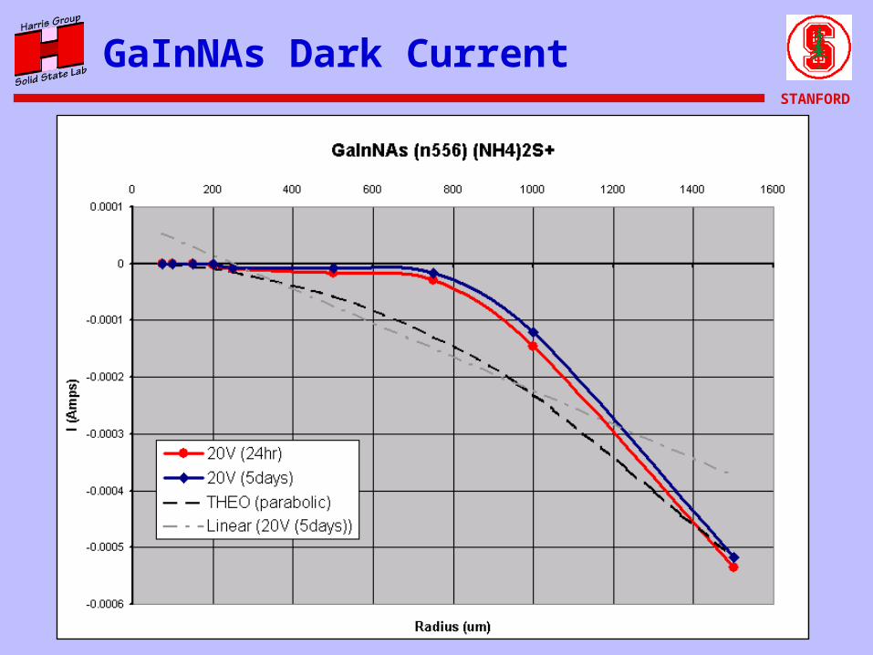
GaInNAs Dark Current
Page 38
STANFORD
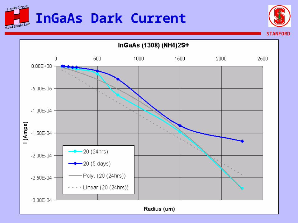
InGaAs Dark Current
Page 39
STANFORD
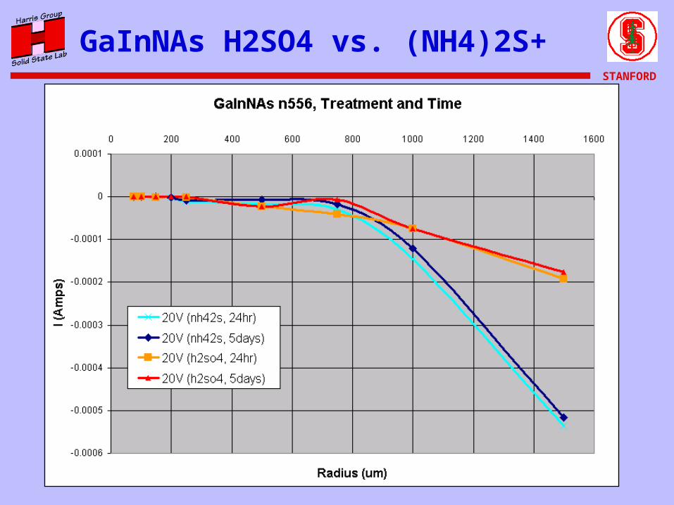
GaInNAs H2SO4 vs. (NH4)2S+
Page 40
STANFORD
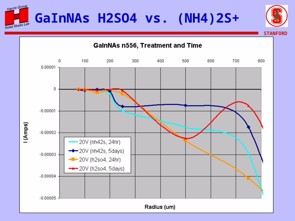
GaInNAs H2SO4 vs. (NH4)2S+
Page 41
STANFORD
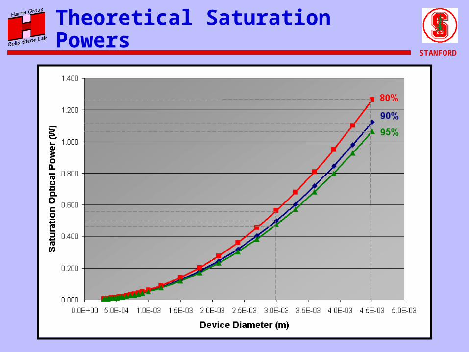
Theoretical Saturation Powers
Page 42
STANFORD
Theoretical Saturation Powers
Page 43
STANFORD
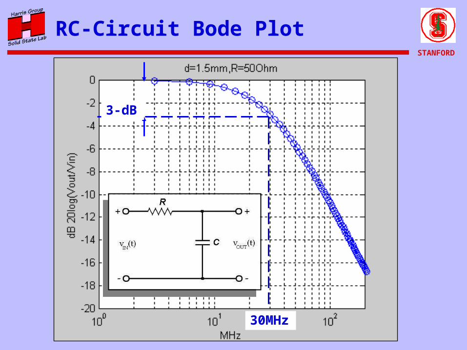
RC-Circuit Bode Plot
3-dB
30MHz
Page 44
STANFORD
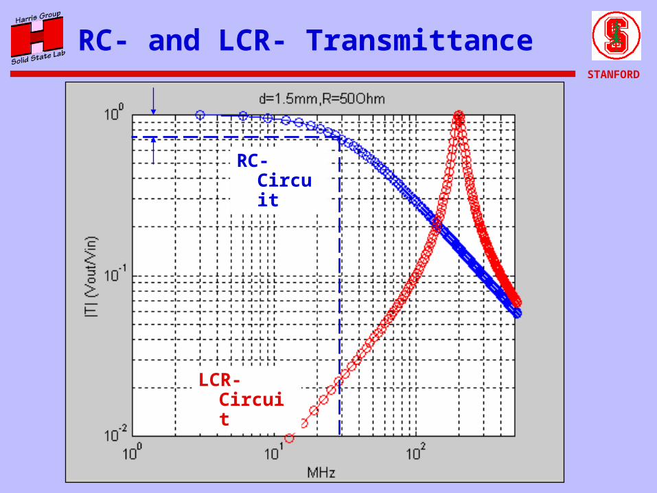
RC- and LCR- Transmittance
RC-Circuit
LCR-Circuit
Page 45
STANFORD
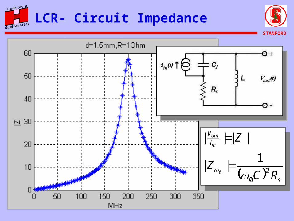
LCR- Circuit Impedance
s
iV
RCZ
Zin
out
20
1||
||||
0
s
iV
RCZ
Zin
out
20
1||
||||
0
Page 46
STANFORD
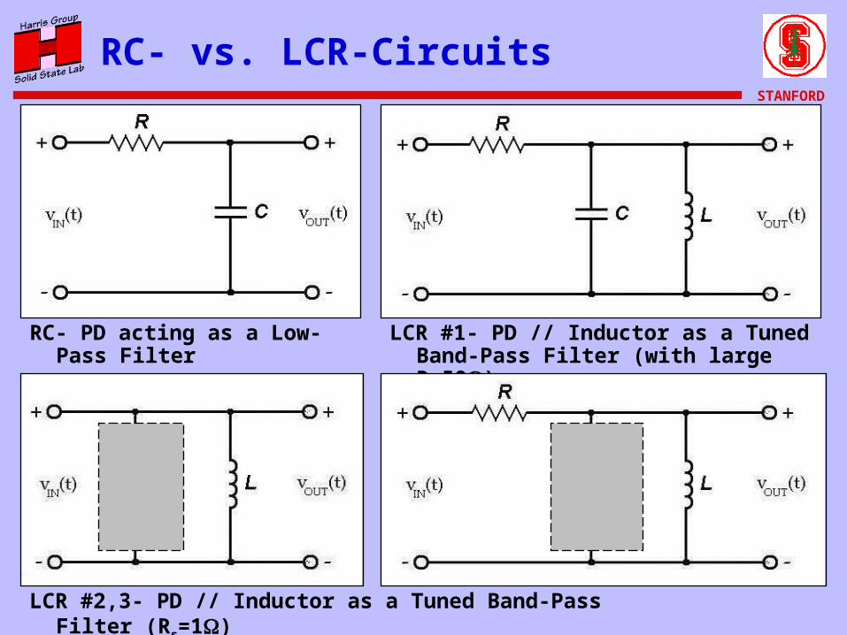
RC- vs. LCR-Circuits
RC- PD acting as a Low-Pass Filter LCR #1- PD // Inductor as a Tuned Band-Pass Filter (with large R=50)
LCR #2,3- PD // Inductor as a Tuned Band-Pass Filter (Rs=1)
Page 47
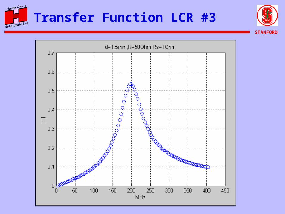
STANFORD
Transfer Function LCR #3