+ All Categories
Home > Documents > “Advanced Silicon Technology Foundry Access … For Public Release, Distribution Unlimited FOR...

“Advanced Silicon Technology Foundry Access … For Public Release, Distribution Unlimited FOR...

Date post: 19-May-2018
Category:
Upload: lamtuyen
View: 242 times
Download: 1 times
Share this document with a friend
13
FOR OFFICIAL USE ONLY – Not Cleared for Open Release Approved For Public Release, Distribution Unlimited “Advanced Silicon Technology Foundry Access Strategy for DoD Research” “Advanced Silicon Technology Foundry Access Strategy for DoD Research” Dr. Mike Fritze DARPA MTO Office Dr. Mike Fritze DARPA MTO Office Approved For Public Release, Distribution Unlimited
Transcript

FOR OFFICIAL USE ONLY – Not Cleared for Open ReleaseApproved For Public Release, Distribution Unlimited

“Advanced Silicon Technology Foundry Access Strategy for DoD Research”

“Advanced Silicon Technology Foundry Access Strategy for DoD Research”

Dr. Mike FritzeDARPA MTO Office

Dr. Mike FritzeDARPA MTO Office

Approved For Public Release, Distribution Unlimited

Report Documentation Page Form ApprovedOMB No. 0704-0188

Public reporting burden for the collection of information is estimated to average 1 hour per response, including the time for reviewing instructions, searching existing data sources, gathering andmaintaining the data needed, and completing and reviewing the collection of information. Send comments regarding this burden estimate or any other aspect of this collection of information,including suggestions for reducing this burden, to Washington Headquarters Services, Directorate for Information Operations and Reports, 1215 Jefferson Davis Highway, Suite 1204, ArlingtonVA 22202-4302. Respondents should be aware that notwithstanding any other provision of law, no person shall be subject to a penalty for failing to comply with a collection of information if itdoes not display a currently valid OMB control number.

1. REPORT DATE MAR 2009 2. REPORT TYPE

3. DATES COVERED 00-00-2009 to 00-00-2009

4. TITLE AND SUBTITLE Advanced Silicon Technology Foundry Access Strategy for DoD Research

5a. CONTRACT NUMBER

5b. GRANT NUMBER

5c. PROGRAM ELEMENT NUMBER

6. AUTHOR(S) 5d. PROJECT NUMBER

5e. TASK NUMBER

5f. WORK UNIT NUMBER

7. PERFORMING ORGANIZATION NAME(S) AND ADDRESS(ES) Defense Advanced Research Projects Agency,Microsystems TechnologyOffice (MTO) ,3701 North Fairfax Drive,Arlington,VA,22203-1714

8. PERFORMING ORGANIZATIONREPORT NUMBER

9. SPONSORING/MONITORING AGENCY NAME(S) AND ADDRESS(ES) 10. SPONSOR/MONITOR’S ACRONYM(S)

11. SPONSOR/MONITOR’S REPORT NUMBER(S)

12. DISTRIBUTION/AVAILABILITY STATEMENT Approved for public release; distribution unlimited

13. SUPPLEMENTARY NOTES MTO (DARPA Microsystems Technology Office) Symposium, 2009, 2-5 Mar 5, San Jose, CA

14. ABSTRACT

15. SUBJECT TERMS

16. SECURITY CLASSIFICATION OF: 17. LIMITATION OF ABSTRACT Same as

Report (SAR)

18. NUMBEROF PAGES

12

19a. NAME OFRESPONSIBLE PERSON

a. REPORT unclassified

b. ABSTRACT unclassified

c. THIS PAGE unclassified

Standard Form 298 (Rev. 8-98) Prescribed by ANSI Std Z39-18

Approved For Public Release, Distribution Unlimited

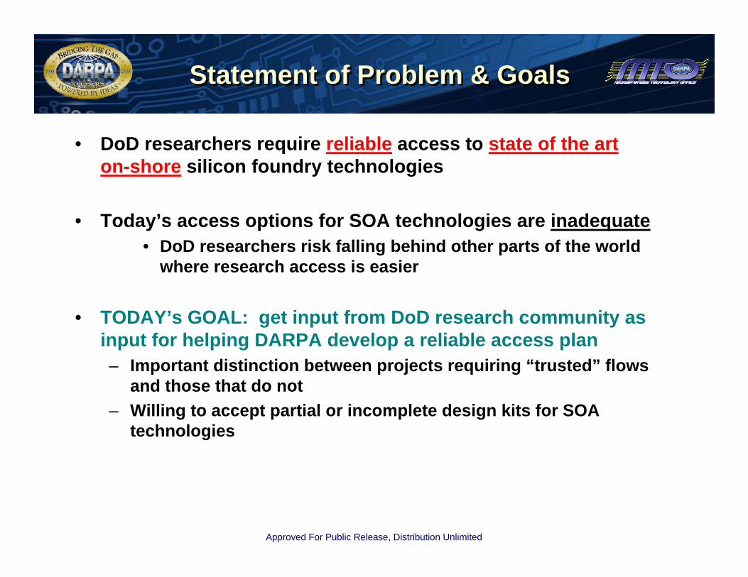
Statement of Problem & GoalsStatement of Problem & Goals

• DoD researchers require reliable access to state of the arton-shore silicon foundry technologies

• Today’s access options for SOA technologies are inadequate• DoD researchers risk falling behind other parts of the world

where research access is easier

• TODAY’s GOAL: get input from DoD research community as input for helping DARPA develop a reliable access plan– Important distinction between projects requiring “trusted” flows

and those that do not– Willing to accept partial or incomplete design kits for SOA

technologies

Approved For Public Release, Distribution Unlimited

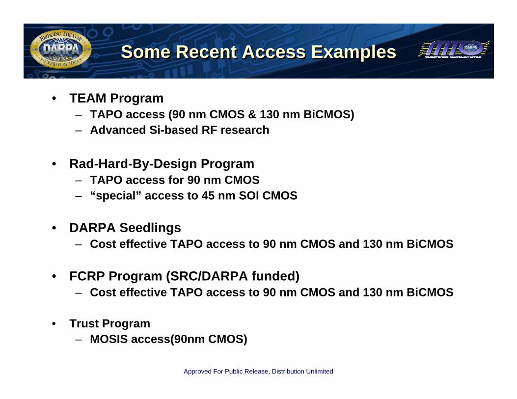
Some Recent Access ExamplesSome Recent Access Examples

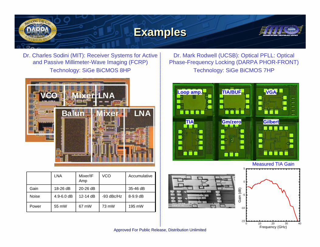
• TEAM Program– TAPO access (90 nm CMOS & 130 nm BiCMOS)– Advanced Si-based RF research

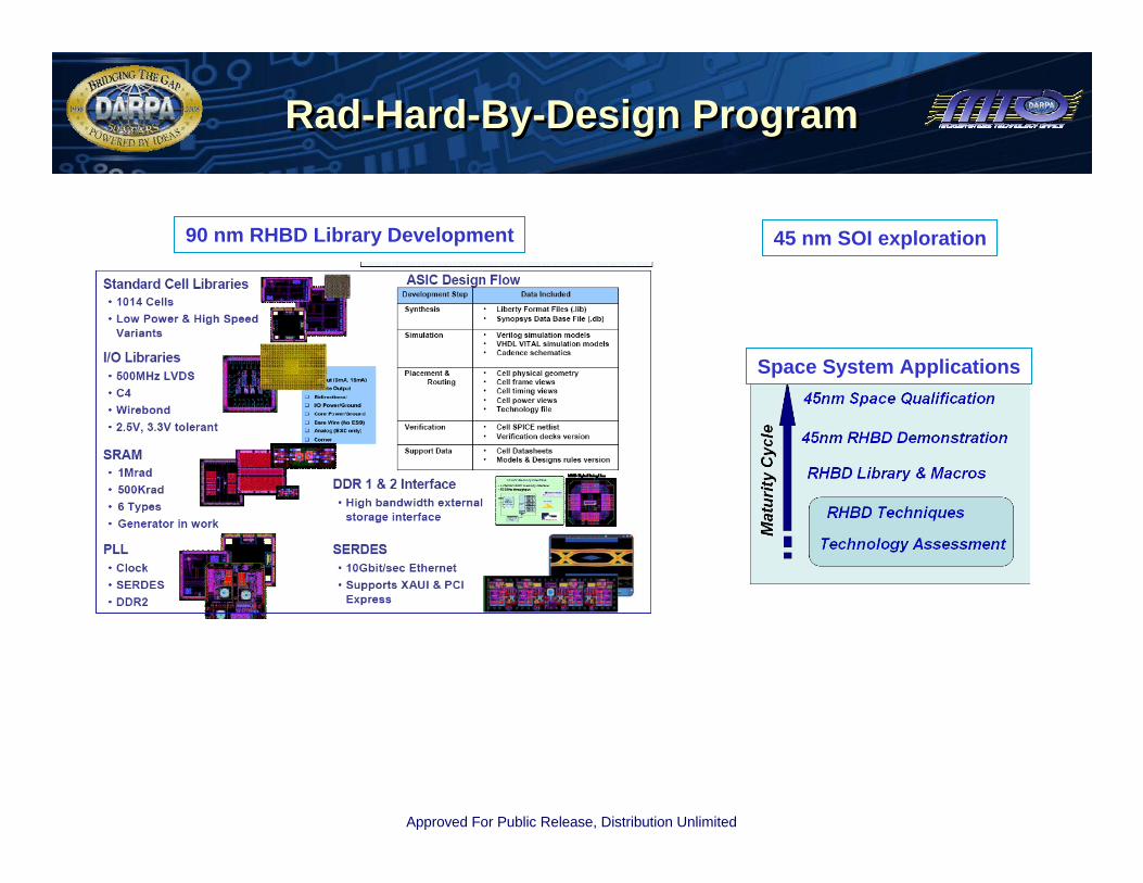
• Rad-Hard-By-Design Program– TAPO access for 90 nm CMOS– “special” access to 45 nm SOI CMOS

• DARPA Seedlings– Cost effective TAPO access to 90 nm CMOS and 130 nm BiCMOS

• FCRP Program (SRC/DARPA funded)– Cost effective TAPO access to 90 nm CMOS and 130 nm BiCMOS

• Trust Program– MOSIS access(90nm CMOS)

Approved For Public Release, Distribution Unlimited

DARPA TEAM PROGRAM:DARPA TEAM PROGRAM:

60 GHz RF-CMOS Rx (TEAM; UCB) Transformer coupled Si-CMOS PA (TEAM; UCB)

60 GHz RF-CMOS Radio (TEAM; GTech) 324 GHz RF-CMOS Oscillator (TEAM; UCLA)

90 nm RF-CMOS

Linear superposition of fourphase-shifted fundamentalsgenerating output at 40

Pwr = -41 dB

90 nm RF-CMOS

GPwr= -8 to +55dBNF = 6.2 dBP1dB(in) = -26 dB Pwr = 24 mWVdd = 1V

90 nm RF-CMOS

Vdd = 1 VP1dB = +9 dBPSat = +12.3 dBArea = 660 x 380 um2

PAE = 8.8%

Rx

Tx 90 nm RF-CMOS

TP = 7 Gb/s (QPSK)TP = 15 Gb/s (16QAMM)Pwr = 200 mW

Approved For Public Release, Distribution Unlimited

Rad-Hard-By-Design ProgramRad-Hard-By-Design Program

Space System Applications

90 nm RHBD Library Development 45 nm SOI exploration

Approved For Public Release, Distribution Unlimited

ExamplesExamples

VCO Mixer LNA

Mixer LNABalun

LNA Mixer/IF Amp

VCO Accumulative

Gain 18-26 dB 20-26 dB 35-46 dB

Noise 4.9-6.0 dB 12-14 dB -93 dBc/Hz 8-9.9 dB

Power 55 mW 67 mW 73 mW 195 mW

Dr. Charles Sodini (MIT): Receiver Systems for Active and Passive Millimeter-Wave Imaging (FCRP)

Technology: SiGe BiCMOS 8HP

TIA/BUF VGA

GilbertGm/zeroTIA

Loop amp.

Dr. Mark Rodwell (UCSB): Optical PFLL: Optical Phase-Frequency Locking (DARPA PHOR-FRONT)

Technology: SiGe BiCMOS 7HP

-15

-10

-5

0

5

0 10 20 30 40

Gai

n (d

B)

Frequency (GHz)

Measured TIA Gain

FOR OFFICIAL USE ONLY – Not Cleared for Open ReleaseApproved For Public Release, Distribution Unlimited

Current DARPA Program IC Foundry Enablement

Current DARPA Program IC Foundry Enablement

Saverio FazzariSaverio Fazzari

Approved For Public Release, Distribution Unlimited

OutlineOutlineOutline

• Requirements– Projects need cost effective and reliable technology access for IC

fabrication– Multiple process node support desired

• Primary options– TAPO

• DOD sponsored IBM access with cost• Limited runs & limited SOA technology

– MOSIS• Large MPW schedule• Costs & limited SOA technology

– Custom Foundry relationships• Large access to specific foundry technologies• Costly for PI to maintain relationship; limited PI pool

Approved For Public Release, Distribution Unlimited

IC Design Flow and TAPOIC Design Flow and TAPO

Product Definition

Modeling

RTL/Analog Design

Synthesis/Simulation

Layout

Aggregation

Mask Making

Physical Implementation

Packaging

Test

Plain Language

RTL

Netlist

GDSII

Silicon

Foundry ASIC Services

In-House Design

The ASIC shall implement a square root function with an 8 bit unsigned magnitude as input and 5-bit unsigned output including 1 fractional bit.

architecture signal A_REAL, Z_REAL : real;

beginA_REAL <= real(A_IN);Z_REAL <= sqrt(A_REAL);Z_OUT <= to_std_ulogic_vector(Z_REAL,5);

end;

IBM & ARM IP

KCP

Foun

dry

Serv

ices

Other DesignsOther Designs

In-H

ouse

In-H

ouse

(Tru

sted

)

Foun

dry

Serv

ices

(Tru

sted

thro

ugh

TAPO

)

Approved For Public Release, Distribution Unlimited

TAPO MPW RunsTAPO MPW Runs

FY09 MPW Program Scheduleas of September 9, 2008

Oct Nov Dec Jan Feb Mar Apr May Jun Jul Aug Sep

8HP 130nm10/01/08 8HP09A

12/08/08 8HP09B

02/09/09 8HP09C

06/08/09 8HP 09D

09/08/09 8HP09E

8RF 130nm11/03/08 8RF09A

03/09/09 8RF09B

05/26/09 8RF 09C

08/10/09 8RF09D

9SF 90nm12/01/08 9SF09A

07/13/09 9SF09C

7HP 180nm10/27/2008

7HP09A04/20/09 7HP 09B

9LP 90nm05/04/09 9LP09A

10SF 65nm02/23/09

10SF09A*

Quarter 4Technology

Quarter 1 Quarter 2 Quarter 3

9SF09B04/06/09

There have been advanced runs including 45 nm SOI (12S0)

* Fully Customer-Funded Run (Taxi-Run)

Approved For Public Release, Distribution Unlimited

IC Design Flow With MOSISIC Design Flow With MOSISIC Design Flow With MOSIS

Product Definition

Modeling

RTL/Analog Design

Synthesis/Simulation

Layout

Aggregation

Mask Making

Physical Implementation

Packaging

Test

Plain Language

RTL

Netlist

GDSII

Silicon

Foundry ASIC Services

In-House Design

The ASIC shall implement a square root function with an 8 bit unsigned magnitude as input and 5-bit unsigned output including 1 fractional bit.

architecture signal A_REAL, Z_REAL : real;

beginA_REAL <= real(A_IN);Z_REAL <= sqrt(A_REAL);Z_OUT <= to_std_ulogic_vector(Z_REAL,5);

end;

Third-Party IP

MOSIS

Foun

dry

Serv

ices

Other DesignsOther Designs

In-H

ouse

In-H

ouse

(Tru

sted

)

Foun

dry

Serv

ices

(Unt

rust

ed)

Approved For Public Release, Distribution Unlimited

MOSIS MPW INFOMOSIS MPW INFOMOSIS MPW INFO

AMIS • The AMIS fabrication schedule includes MPW runs in the

following processes: 1.5 µm CMOS, 0.7 µm high voltage CMOS, 0.5 µm CMOS, and 0.35 µm high voltage CMOS.

austriamicrosystems• The austriamicrosystems fabrication schedule offered by MOSIS

include 0.35 µm CMOS, high voltage CMOS, and SiGe BiCMOSprocesses.

IBM Fabrication Schedule • The technologies included in the IBM MPW fabrication schedule

range from 45 nanometer to 0.25 µm in CMOS, and from 0.13 µm to 0.50 µm in SiGe BiCMOS.

TSMC Fabrication Schedule • Multiproject wafer (MPW) runs available through TSMC include

0.35 µm CMOS, 0.25 µm CMOS, 0.18 µm CMOS, and 0.13 µm CMOS.

Info from www.mosis.com


Recommended