Page 1
Advanced Technologies for Highly Integrated RFIC Modules for Future Wireless
Communications
Deuk Hyoun Heo Ph. D.
January 22, 2003
Department of Electrical and Computer EngineeringWINLAB
Rutgers University, Piscataway, NJ
Page 2
Georgia Tech
• Location: Atlanta, Georgia USA
– Masters Golf Tournament
– Coca-Cola Headquarters
– Delta
– CNN Headquarters
– Atlanta Braves Baseball
Georgia Institute of Technology
Page 3
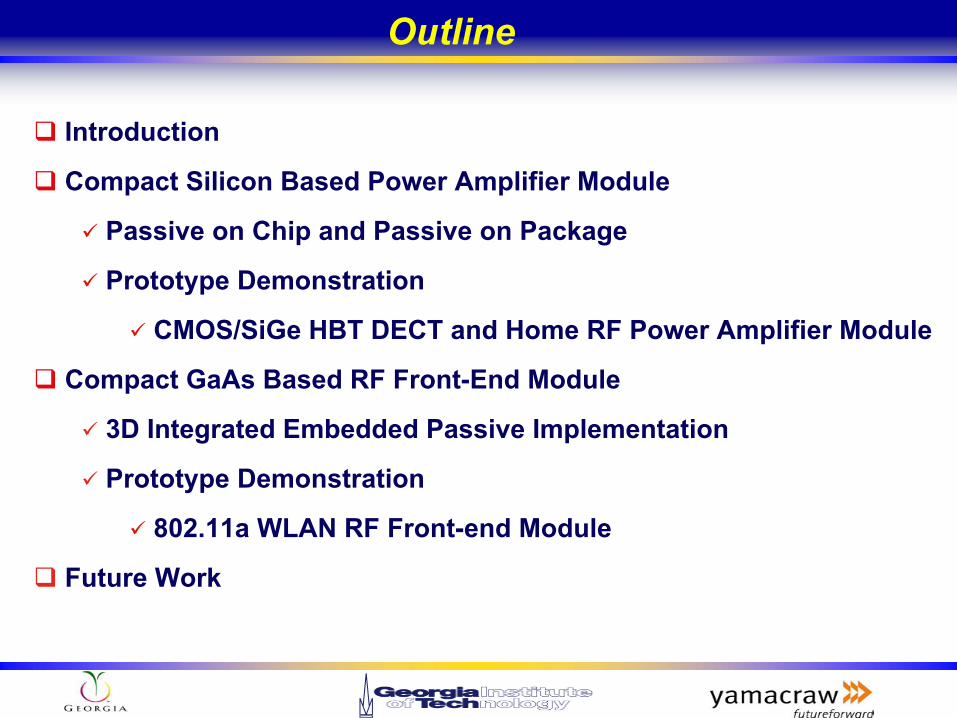
Introduction
Compact Silicon Based Power Amplifier Module
Passive on Chip and Passive on Package
Prototype Demonstration
CMOS/SiGe HBT DECT and Home RF Power Amplifier Module
Compact GaAs Based RF Front-End Module
3D Integrated Embedded Passive Implementation
Prototype Demonstration
802.11a WLAN RF Front-end Module
Future Work
Outline
Page 4
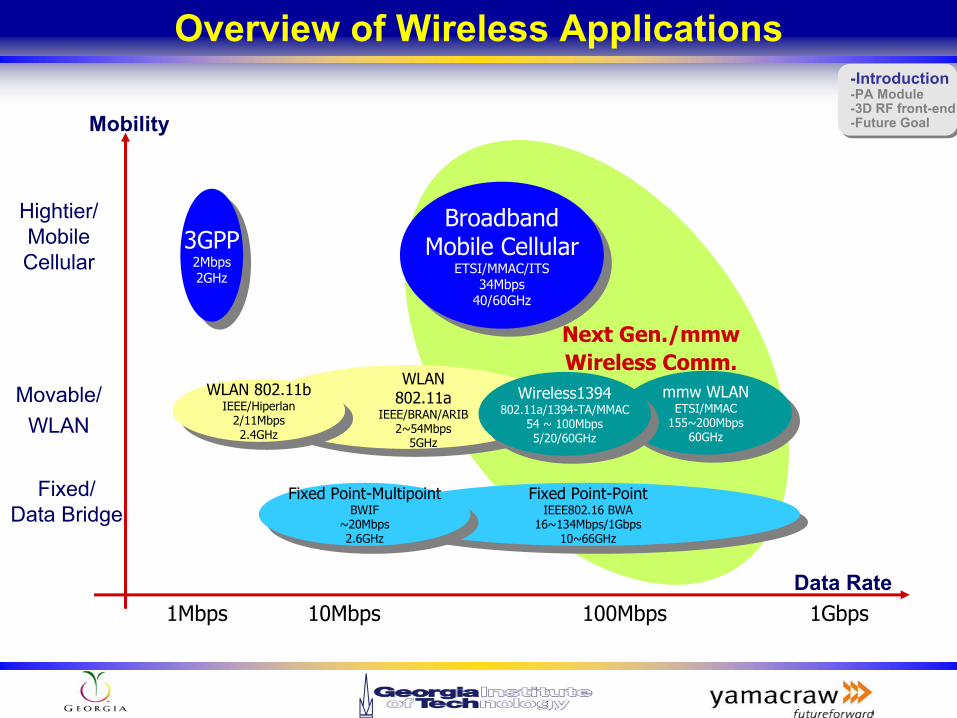
Overview of Wireless Applications
3GPP2Mbps2GHz
3GPP2Mbps2GHz
BroadbandMobile Cellular
ETSI/MMAC/ITS34Mbps
40/60GHz
BroadbandMobile Cellular
ETSI/MMAC/ITS34Mbps
40/60GHz
mmw WLANETSI/MMAC
155~200Mbps60GHz
mmw WLANETSI/MMAC
155~200Mbps60GHz
Fixed Point-PointIEEE802.16 BWA
16~134Mbps/1Gbps10~66GHz
Fixed Point-PointIEEE802.16 BWA
16~134Mbps/1Gbps10~66GHz
10Mbps 100Mbps 1Gbps1Mbps
Fixed Point-MultipointBWIF
~20Mbps2.6GHz
Fixed Point-MultipointBWIF
~20Mbps2.6GHz
WLAN 802.11a
IEEE/BRAN/ARIB2~54Mbps
5GHz
WLAN 802.11bIEEE/Hiperlan
2/11Mbps2.4GHz
WLAN 802.11bIEEE/Hiperlan
2/11Mbps2.4GHz
Wireless1394802.11a/1394-TA/MMAC
54 ~ 100Mbps5/20/60GHz
Wireless1394802.11a/1394-TA/MMAC
54 ~ 100Mbps5/20/60GHz
Hightier/MobileCellular
Movable/WLAN
Fixed/Data Bridge
Mobility
Data Rate
Next Gen./mmw Wireless Comm.
-Introduction-PA Module-3D RF front-end-Future Goal
-Introduction-PA Module-3D RF front-end-Future Goal
Page 5
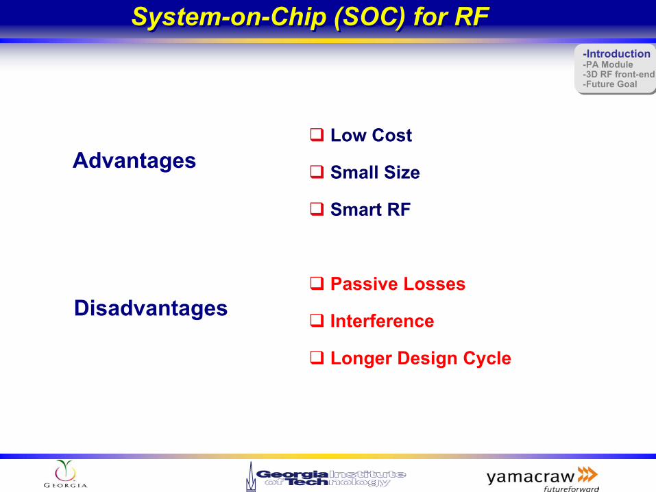
Low Cost
Small Size
Smart RF
Passive Losses
Interference
Longer Design Cycle
System-on-Chip (SOC) for RFSystem-on-Chip (SOC) for RF
Advantages
Disadvantages
-Introduction-PA Module-3D RF front-end-Future Goal
-Introduction-PA Module-3D RF front-end-Future Goal
Page 6
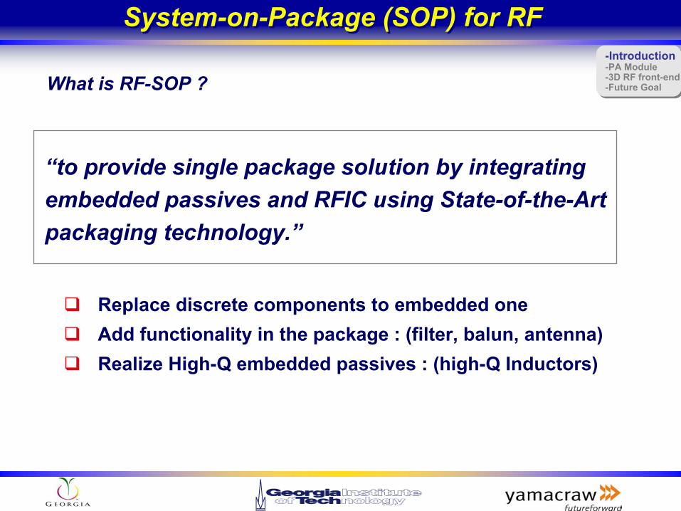
Replace discrete components to embedded oneAdd functionality in the package : (filter, balun, antenna)Realize High-Q embedded passives : (high-Q Inductors)
“to provide single package solution by integrating embedded passives and RFIC using State-of-the-Art packaging technology.”
System-on-Package (SOP) for RFSystem-on-Package (SOP) for RF
What is RF-SOP ?-Introduction-PA Module-3D RF front-end-Future Goal
-Introduction-PA Module-3D RF front-end-Future Goal
Page 7
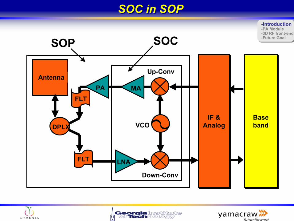
SOC in SOPSOC in SOP
AntennaUp-Conv
PA
LNA
Down-Conv
VCOBasebandBaseband
IF &Analog
IF &Analog
FLT
FLT
MA
DPLX
SOP SOC-Introduction-PA Module-3D RF front-end-Future Goal
-Introduction-PA Module-3D RF front-end-Future Goal
Page 8
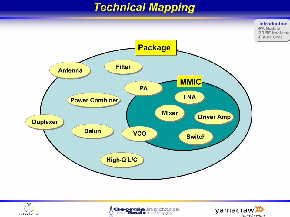
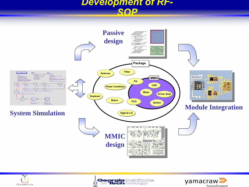
MMIC
PackagePackage
LNALNA
MixerMixer
VCOVCO
PAPA
AntennaAntenna FilterFilter
BalunBalun
High-Q L/CHigh-Q L/C
Driver AmpDriver AmpDuplexerDuplexer
SwitchSwitch
Power CombinerPower Combiner
Technical Mapping-Introduction-PA Module-3D RF front-end-Future Goal
-Introduction-PA Module-3D RF front-end-Future Goal
Page 9
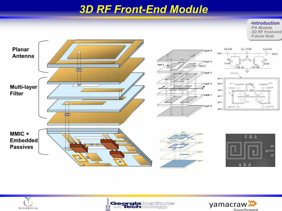
MMIC + Embedded Passives
Multi-layer Filter
PlanarAntenna
3D RF Front-End Module -Introduction-PA Module-3D RF front-end-Future Goal
-Introduction-PA Module-3D RF front-end-Future Goal
Page 10
Development of RF-SOP
System SimulationModule Integration
MMIC design
Passive design
MMIC
PackagePackage
LNALNA
MixerMixer
VCOVCO
PAPA
AntennaAntenna FilterFilter
BalunBalun
High-Q L/CHigh-Q L/C
Driver AmpDriver AmpDuplexerDuplexer
SwitchSwitch
Power CombinerPower Combiner
Page 11
• Compact Silicon Based PowerAmplifier Modules
Page 12
Introduction
Power Amplifiers in RF transmitters
Consume Most of Power in Transmission Mode
Linearity
Cost
Cost Reduction Strategy
Silicon-Based Technology
High levels of Integration
-IntroductionPA Module-3D RF front-end-Future Goal
-IntroductionPA Module-3D RF front-end-Future Goal
Page 13
Issues of CMOS PA
Transistor Characteristics
Low Breakdown Voltage
High Knee Voltage
Passive Component
Lossy Si substrate
Thin Metal Layers
-IntroductionPA Module-3D RF front-end-Future Goal
-IntroductionPA Module-3D RF front-end-Future Goal
Page 14
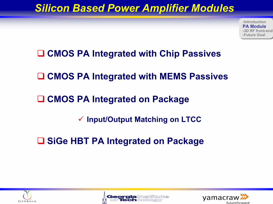
Silicon Based Power Amplifier Modules
CMOS PA Integrated with Chip Passives
CMOS PA Integrated with MEMS Passives
CMOS PA Integrated on Package
Input/Output Matching on LTCC
SiGe HBT PA Integrated on Package
-IntroductionPA Module-3D RF front-end-Future Goal
-IntroductionPA Module-3D RF front-end-Future Goal
Page 15
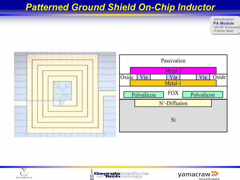
Patterned Ground Shield On-Chip Inductor
FOX+-Diffusion
OxideOxide
Si
Via Via
PolysiliconFOX
ViaMetal-1
Metal-2
Passivation
PolysiliconN+-Diffusion
OxideOxide
Si
Via Via
Polysilicon
-IntroductionPA Module-3D RF front-end-Future Goal
-IntroductionPA Module-3D RF front-end-Future Goal
Page 16
Poly-Silicon Patterned Ground
Q of the Inductor with PG is lower than that of the Inductor without PG.
The Inductor Trace Close to PG introduces Additional Parasitic Capacitance
Additional Parasitic Capacitance degrades the Q of the Inductor
-IntroductionPA Module-3D RF front-end-Future Goal
-IntroductionPA Module-3D RF front-end-Future Goal
Page 17
Improvement of Patterned Ground
N+-Diffusion layer is used to implement PG
Much less Parasitic Capacitance is introduced by
N+-Diffusion PG
Q can be enhanced up to 20%
Effective Inductance is not affected by PG
-IntroductionPA Module-3D RF front-end-Future Goal
-IntroductionPA Module-3D RF front-end-Future Goal
Page 18
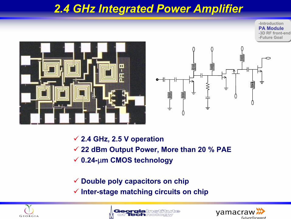
2.4 GHz Integrated Power Amplifier
2.4 GHz, 2.5 V operation22 dBm Output Power, More than 20 % PAE0.24-µm CMOS technology
Double poly capacitors on chipInter-stage matching circuits on chip
-IntroductionPA Module-3D RF front-end-Future Goal
-IntroductionPA Module-3D RF front-end-Future Goal
Page 19
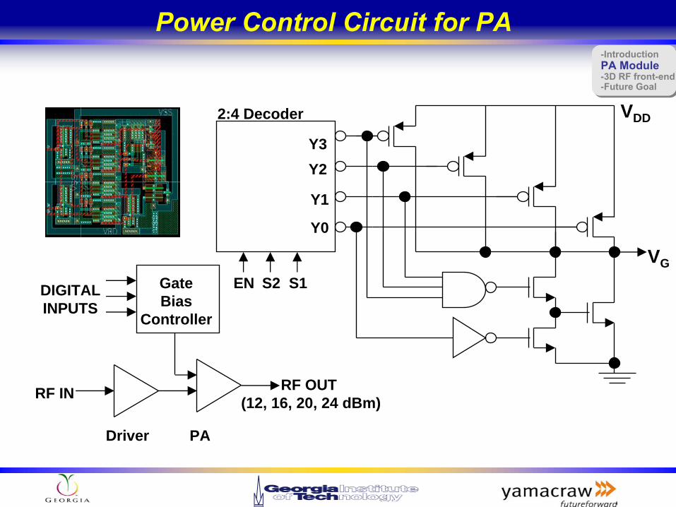
2:4 Decoder
EN S2 S1
Y3
Y2
Y1
Y0
VG
VDD
Driver PA
RF OUT (12, 16, 20, 24 dBm)
RF IN
GateBias
Controller
DIGITALINPUTS
Power Control Circuit for PA-IntroductionPA Module-3D RF front-end-Future Goal
-IntroductionPA Module-3D RF front-end-Future Goal
Page 20
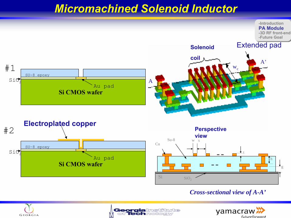
Micromachined Solenoid Inductor
w s
t
h
Si
g
Su-8Cu
SiO2
wc
Solenoid
coil
A
A’
Extended pad
Perspective view
Cross-sectional view of A-A’
Si CMOS wafer
SU-8 epoxy
SiO2Au pad
Si CMOS wafer
Electroplated copper
SU-8 epoxy
SiO2Au pad
#1
#2
-IntroductionPA Module-3D RF front-end-Future Goal
-IntroductionPA Module-3D RF front-end-Future Goal
Page 21
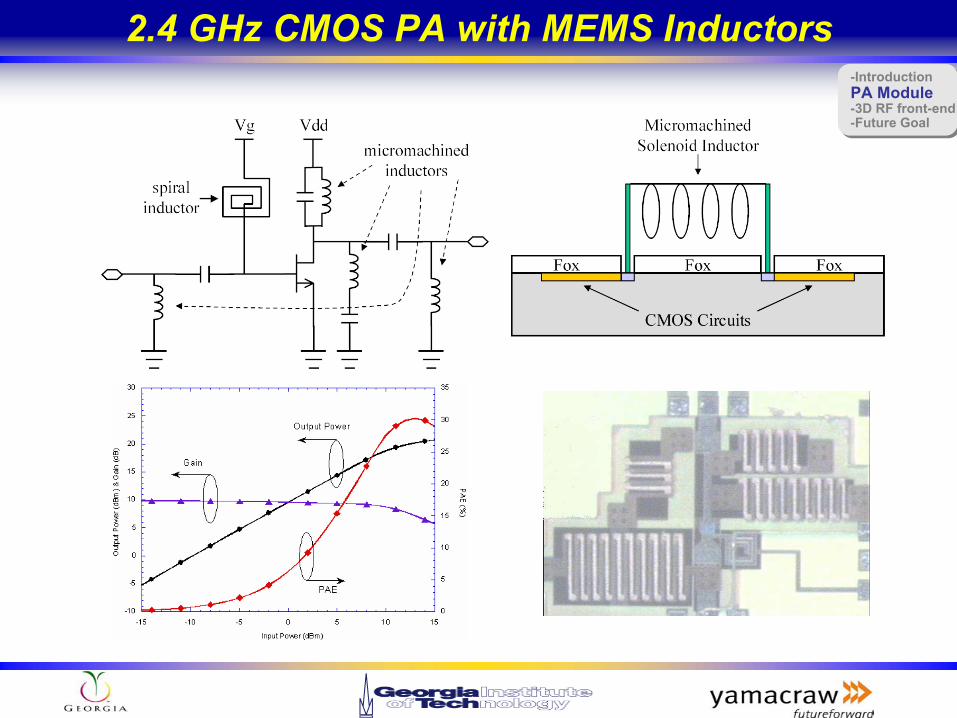
2.4 GHz CMOS PA with MEMS Inductors-IntroductionPA Module-3D RF front-end-Future Goal
-IntroductionPA Module-3D RF front-end-Future Goal
Page 22
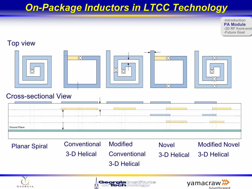
On-Package Inductors in LTCC Technology
Ground Plane
Top view
Cross-sectional View
Planar Spiral Conventional3-D Helical
Modified Conventional3-D Helical
Novel 3-D Helical
Modified Novel 3-D Helical
-IntroductionPA Module-3D RF front-end-Future Goal
-IntroductionPA Module-3D RF front-end-Future Goal
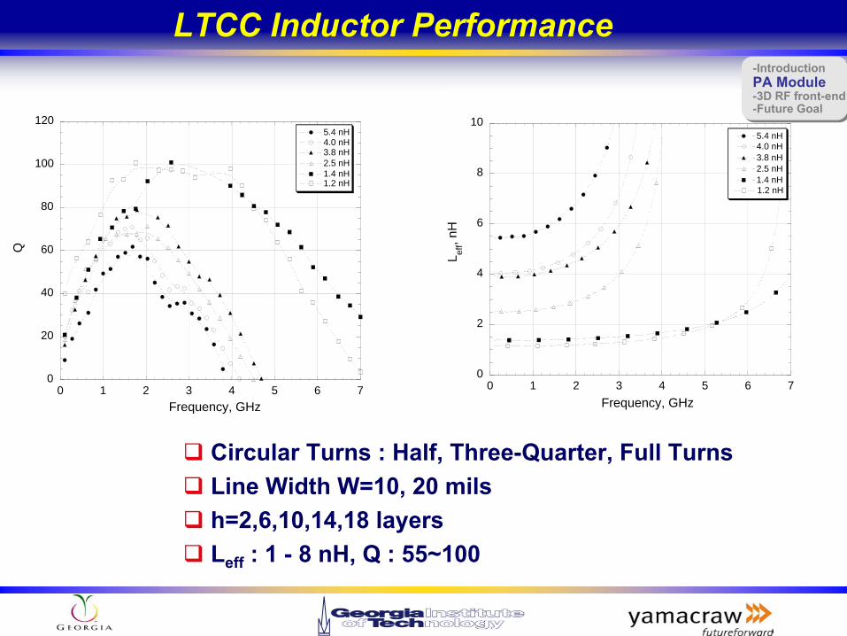
Page 23
0
20
40
60
80
100
120
0 1 2 3 4 5 6 7
4.0 nH5.4 nH
2.5 nH3.8 nH
1.2 nH1.4 nH
Q
Frequency, GHz
0
2
4
6
8
10
0 1 2 3 4 5 6 7
4.0 nH5.4 nH
2.5 nH 3.8 nH
1.2 nH1.4 nH
L eff, n
H
Frequency, GHz
Circular Turns : Half, Three-Quarter, Full TurnsLine Width W=10, 20 milsh=2,6,10,14,18 layersLeff : 1 - 8 nH, Q : 55~100
LTCC Inductor Performance-IntroductionPA Module-3D RF front-end-Future Goal
-IntroductionPA Module-3D RF front-end-Future Goal
Page 24
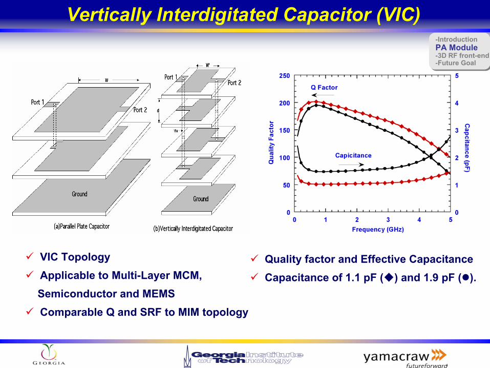
Vertically Interdigitated Capacitor (VIC)
VIC TopologyApplicable to Multi-Layer MCM,Semiconductor and MEMSComparable Q and SRF to MIM topology
Quality factor and Effective Capacitance Capacitance of 1.1 pF ( ) and 1.9 pF ( ).
-IntroductionPA Module-3D RF front-end-Future Goal
-IntroductionPA Module-3D RF front-end-Future Goal
Page 25
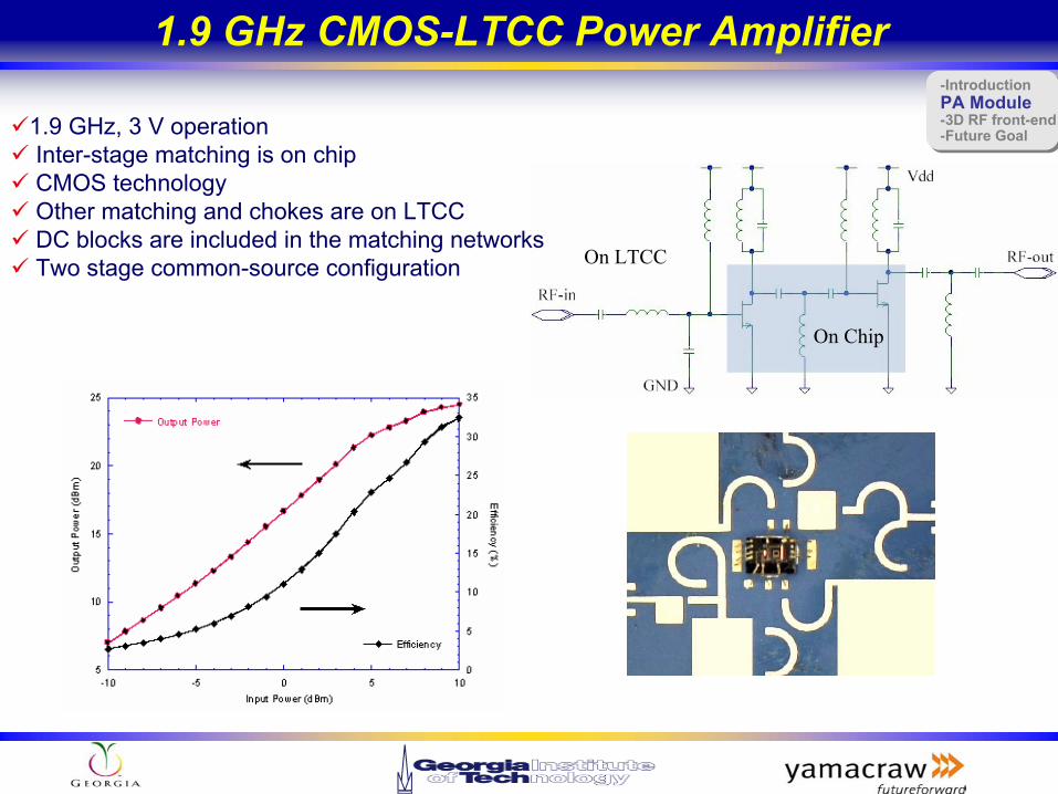
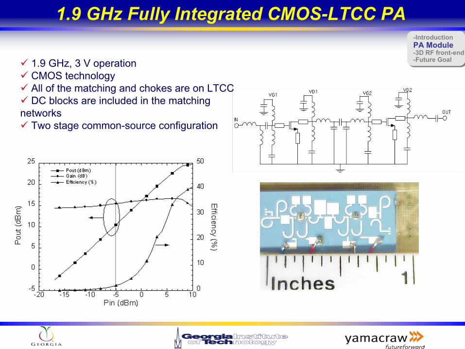
1.9 GHz CMOS-LTCC Power Amplifier
On Chip
On LTCC
1.9 GHz, 3 V operationInter-stage matching is on chipCMOS technologyOther matching and chokes are on LTCCDC blocks are included in the matching networksTwo stage common-source configuration
-IntroductionPA Module-3D RF front-end-Future Goal
-IntroductionPA Module-3D RF front-end-Future Goal
Page 26
1.9 GHz Fully Integrated CMOS-LTCC PA
1.9 GHz, 3 V operationCMOS technologyAll of the matching and chokes are on LTCCDC blocks are included in the matching
networks Two stage common-source configuration
-IntroductionPA Module-3D RF front-end-Future Goal
-IntroductionPA Module-3D RF front-end-Future Goal
Page 27
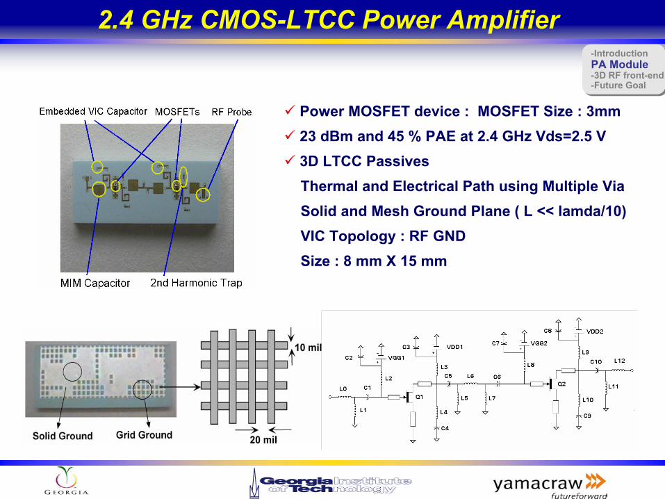
2.4 GHz CMOS-LTCC Power Amplifier
Power MOSFET device : MOSFET Size : 3mm 23 dBm and 45 % PAE at 2.4 GHz Vds=2.5 V 3D LTCC Passives Thermal and Electrical Path using Multiple ViaSolid and Mesh Ground Plane ( L << lamda/10)VIC Topology : RF GNDSize : 8 mm X 15 mm
-IntroductionPA Module-3D RF front-end-Future Goal
-IntroductionPA Module-3D RF front-end-Future Goal
Page 28
Power Amplifier in a Si-based Technology
SiGe HBT ⇒ HBT Device Advantages in Si
Enhance Native Device Performance
Class F-like Loading ⇒ High EfficiencyHarmonic Suppression Filter (HSF)
-3-
SiGe HBT Power Amplifier-IntroductionPA Module-3D RF front-end-Future Goal
-IntroductionPA Module-3D RF front-end-Future Goal
Page 29
Load impedanceSecond Harmonic ShortOpen at Third harmonic
Performance Enhancements0.6 dB Additional powerNo power Dissipation at Harmonics90 % Efficiency
NeededCompact Implementation of Load Network
-5-
Class F Operation-IntroductionPA Module-3D RF front-end-Future Goal
-IntroductionPA Module-3D RF front-end-Future Goal
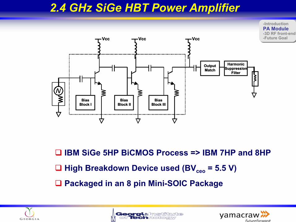
Page 30
Bias Block II
Bias Block I
Bias Block III
Output Match
Harmonic Suppression
Filter
Vcc Vcc Vcc
Bias Block II
Bias Block I
Bias Block III
Output Match
Harmonic Suppression
Filter
Vcc Vcc Vcc
IBM SiGe 5HP BiCMOS Process => IBM 7HP and 8HP
High Breakdown Device used (BVceo = 5.5 V)
Packaged in an 8 pin Mini-SOIC Package
-10-
2.4 GHz SiGe HBT Power Amplifier-IntroductionPA Module-3D RF front-end-Future Goal
-IntroductionPA Module-3D RF front-end-Future Goal
Page 31
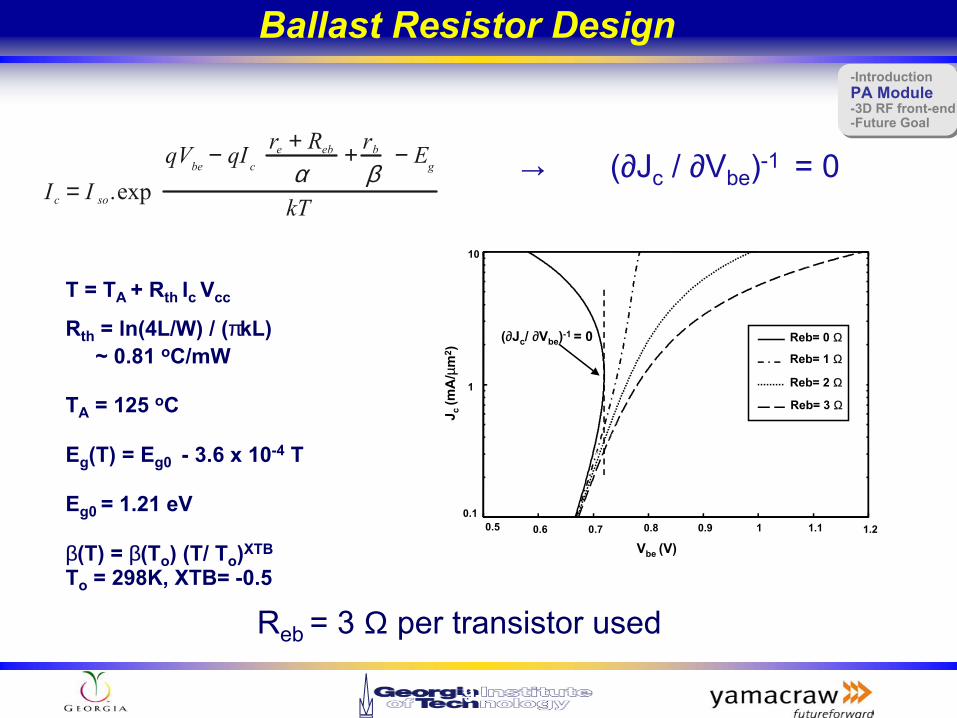
Ic = I so.expqVbe − qIc
re + Rebα
+ rbβ
− Eg
kT
T = TA + Rth Ic Vcc
Rth = ln(4L/W) / (πkL) ~ 0.81 oC/mW
TA = 125 oC
Eg(T) = Eg0 - 3.6 x 10⁻⁴ T
Eg0 = 1.21 eV
β(T) = β(To) (T/ To)XTB
To = 298K, XTB= -0.5
→ (∂Jc / ∂Vbe)-1 = 0
Reb = 3 Ω per transistor used
-9-
Ballast Resistor Design
0.5 0.6 0.7 0.8 0.9 1 1.1 1.20.1
1
10
Reb= 0 Ω
Reb= 1 Ω
Reb= 2 Ω
(∂Jc/ ∂Vbe)-1 = 0
Vbe (V)
J c (m
A/µ
m2 )
Reb= 3 Ω
-IntroductionPA Module-3D RF front-end-Future Goal
-IntroductionPA Module-3D RF front-end-Future Goal
Page 32
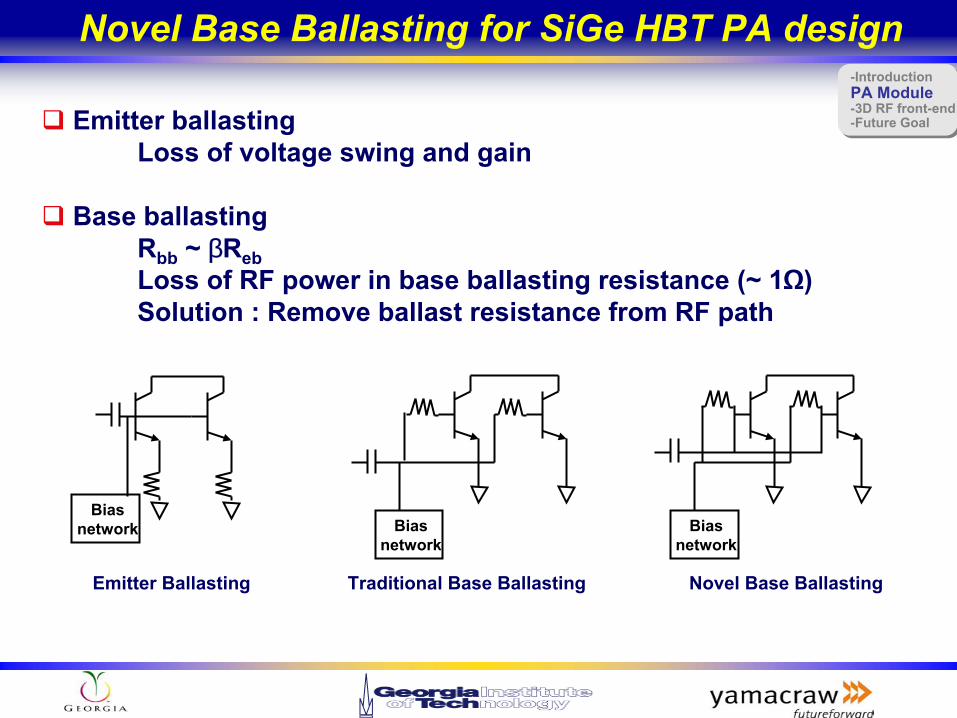
Novel Base Ballasting for SiGe HBT PA design
Emitter ballasting Loss of voltage swing and gain
Base ballastingRbb ~ βRebLoss of RF power in base ballasting resistance (~ 1Ω)Solution : Remove ballast resistance from RF path
Bias network
Bias network Bias
network
Emitter Ballasting Traditional Base Ballasting Novel Base Ballasting
-IntroductionPA Module-3D RF front-end-Future Goal
-IntroductionPA Module-3D RF front-end-Future Goal
Page 33
Biasing for SiGe HBT PAs
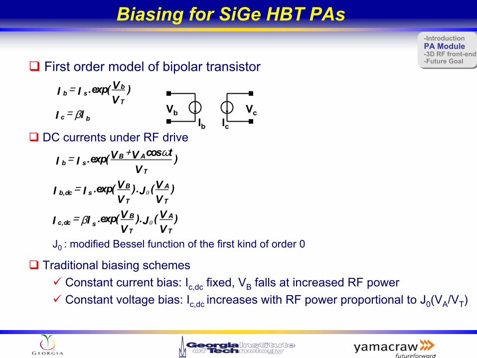
First order model of bipolar transistor
bI = sI .exp( bV
TV)
cI = bβIIb Ic
Vb Vc
bI = sI .exp( BV + AV cosωt
TV)
b,dcI = sI .exp( BV
TV). 0J ( AV
TV)
c,dcI = sβI .exp( BV
TV). 0J ( AV
TV)
DC currents under RF drive
Traditional biasing schemesConstant current bias: Ic,dc fixed, VB falls at increased RF powerConstant voltage bias: Ic,dc increases with RF power proportional to J0(VA/VT)
J0 : modified Bessel function of the first kind of order 0
-IntroductionPA Module-3D RF front-end-Future Goal
-IntroductionPA Module-3D RF front-end-Future Goal
Page 34
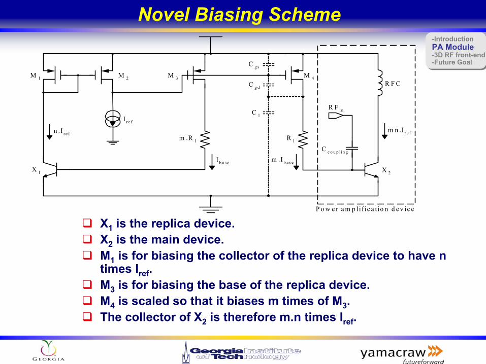
Novel Biasing Scheme
M 1 M 2 M 3 M 4
X 1
I re f
n .I re f
X 2
I b a s e m .I b a s e
R 1m .R 1
C 1
C g d
C g s
C c o u p lin g
R F in
m n .I re f
R F C
P o w e r a m p li f ic a t io n d e v ic e
X1 is the replica device.X2 is the main device.M1 is for biasing the collector of the replica device to have n times Iref.M3 is for biasing the base of the replica device.M4 is scaled so that it biases m times of M3.The collector of X2 is therefore m.n times Iref.
-IntroductionPA Module-3D RF front-end-Future Goal
-IntroductionPA Module-3D RF front-end-Future Goal
Page 35
Insensitivity to Process, Voltage, and Temperature
The Iref is generated from the bandgap voltage reference over an external resistor (not shown in schematic). Therefore, it is constant over the change of biasing voltage
Biasing currents are only dependent on the ratio of transistors,it is therefore insensitive to the process variation such as gm
and VT
The temperature dependent gm and VT do not have any role in this biasing scheme, so it does not change the biasing currents over the change of temperature
-IntroductionPA Module-3D RF front-end-Future Goal
-IntroductionPA Module-3D RF front-end-Future Goal
Page 36
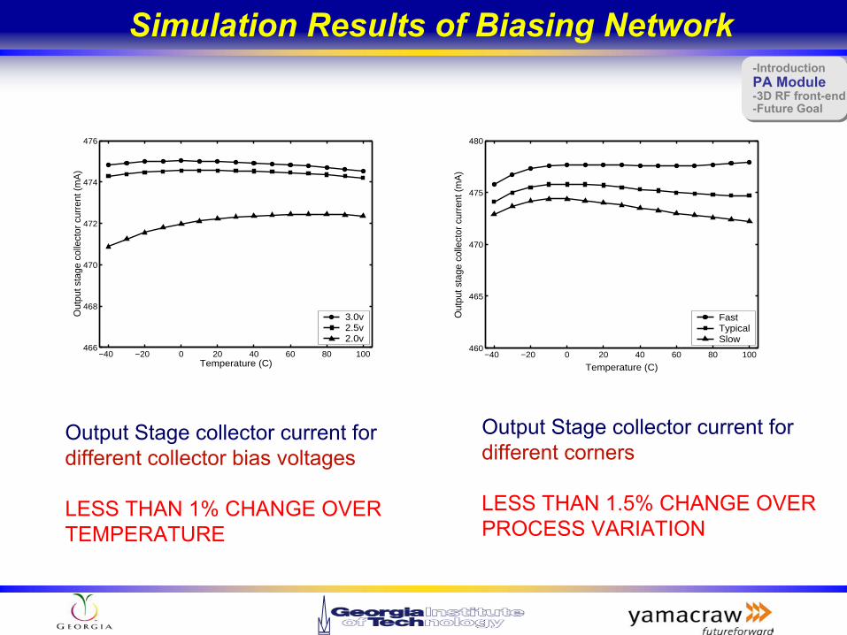
Simulation Results of Biasing Network
−40 −20 0 20 40 60 80 100466
468
470
472
474
476
Temperature (C)
Out
put s
tage
col
lect
or c
urre
nt (
mA
)
3.0v2.5v2.0v
−40 −20 0 20 40 60 80 100460
465
470
475
480
Temperature (C)
Out
put s
tage
col
lect
or c
urre
nt (
mA
)
FastTypicalSlow
Output Stage collector current fordifferent corners
LESS THAN 1.5% CHANGE OVERPROCESS VARIATION
Output Stage collector current fordifferent collector bias voltages
LESS THAN 1% CHANGE OVERTEMPERATURE
-IntroductionPA Module-3D RF front-end-Future Goal
-IntroductionPA Module-3D RF front-end-Future Goal
Page 37
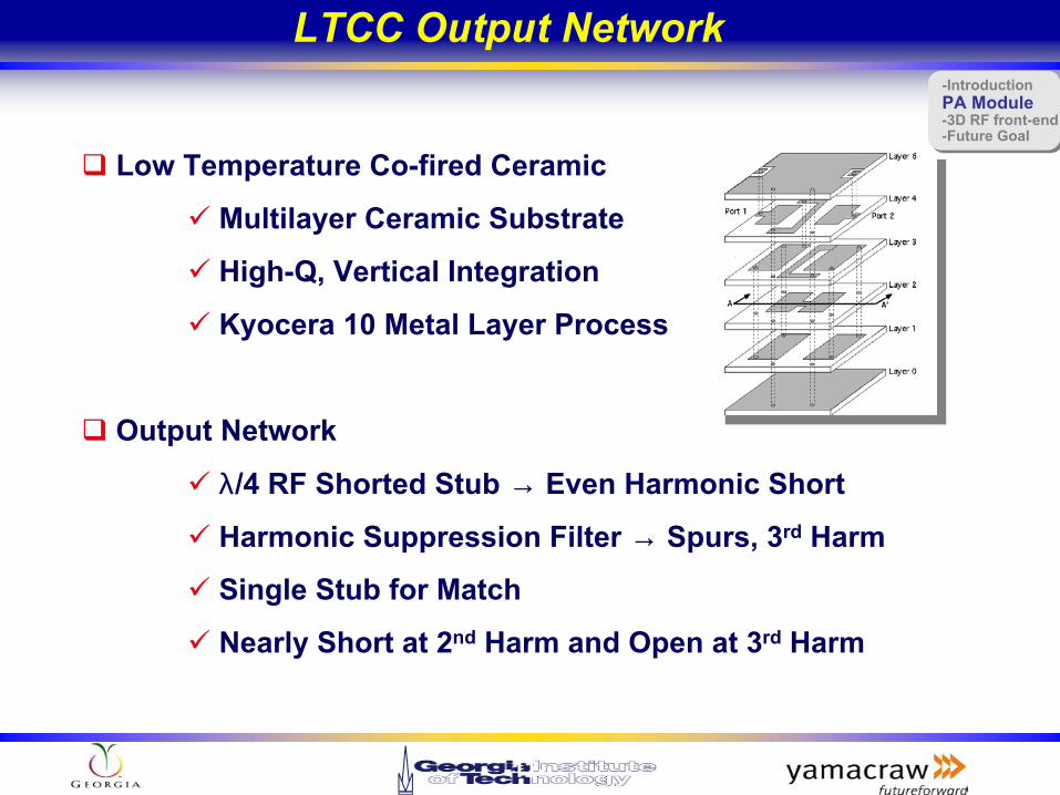
Low Temperature Co-fired Ceramic
Multilayer Ceramic Substrate
High-Q, Vertical Integration
Kyocera 10 Metal Layer Process
Output Network
λ/4 RF Shorted Stub → Even Harmonic Short
Harmonic Suppression Filter → Spurs, 3rd Harm
Single Stub for Match
Nearly Short at 2nd Harm and Open at 3rd Harm
-12-
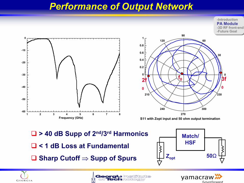
LTCC Output Network-IntroductionPA Module-3D RF front-end-Future Goal
-IntroductionPA Module-3D RF front-end-Future Goal
Page 38
-60
-50
-40
-30
-20
-10
0
1 2 3 4 5 6 7 8Frequency (GHz)
> 40 dB Supp of 2nd/3rd Harmonics
< 1 dB Loss at Fundamental
Sharp Cutoff ⇒ Supp of Spurs
0
0.2
0.4
0.6
0.8
1
0
30
60
90
120
210
240
270
300
330
S11 with Zopt input and 50 ohm output termination
f02f0
3f0
Match/HSF
Zopt 50Ω
-14-
Performance of Output Network-IntroductionPA Module-3D RF front-end-Future Goal
-IntroductionPA Module-3D RF front-end-Future Goal
Page 39
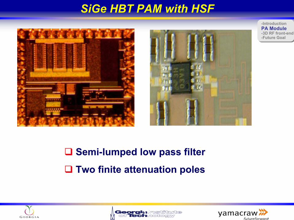
SiGe HBT PAM with HSF
Semi-lumped low pass filter
Two finite attenuation poles
-13-
0.5”
0.75”
-IntroductionPA Module-3D RF front-end-Future Goal
-IntroductionPA Module-3D RF front-end-Future Goal
Page 40
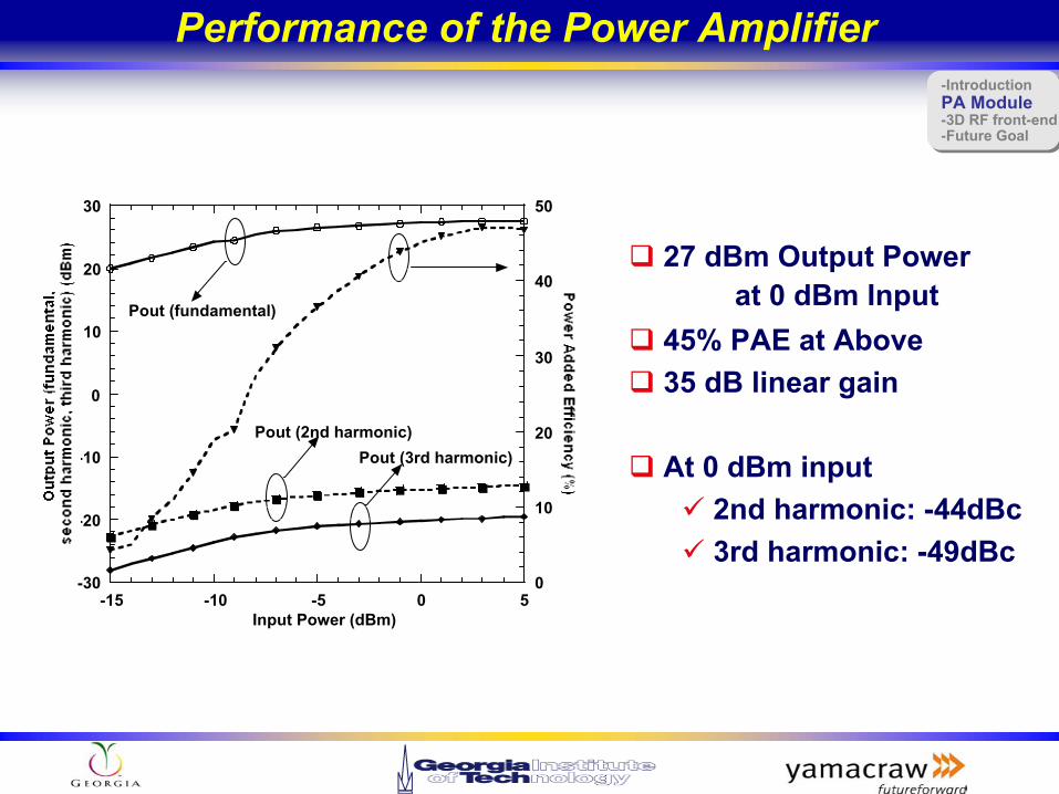
27 dBm Output Power at 0 dBm Input
45% PAE at Above35 dB linear gain
At 0 dBm input2nd harmonic: -44dBc3rd harmonic: -49dBc
-30
-20
-10
0
10
20
30
0
10
20
30
40
50
-15 -10 -5 0 5Input Power (dBm)
Pout (fundamental)
Pout (2nd harmonic)Pout (3rd harmonic)
Performance of the Power Amplifier-IntroductionPA Module-3D RF front-end-Future Goal
-IntroductionPA Module-3D RF front-end-Future Goal
Page 41
Demonstration of Silicon-Based Power Amplifiers
with Different level of Integration towards RF SOP
Integrated on chip with chip Passives
Integrated on chip with MEMS Passives
Integrated on Package
Fully Integrated on Package
-18-
Summary-IntroductionPA Module-3D RF front-end-Future Goal
-IntroductionPA Module-3D RF front-end-Future Goal
Page 42
• Compact RF Front-end Module for IEEE 802.11a WLAN
Applications
Page 43
Motivation/Objectives
Demand for high data rates, broadband transmission
Significant RF interference within 2.4 GHz
802.11a more attractive for their high data rates in
densely populated area
Short coverage, more access points needed
Need for low cost RF front-end module
Page 44
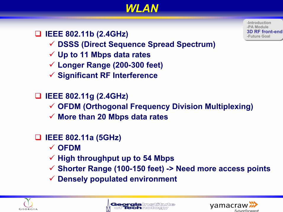
WLAN
IEEE 802.11b (2.4GHz)DSSS (Direct Sequence Spread Spectrum)Up to 11 Mbps data ratesLonger Range (200-300 feet)Significant RF Interference
IEEE 802.11g (2.4GHz)OFDM (Orthogonal Frequency Division Multiplexing)More than 20 Mbps data rates
IEEE 802.11a (5GHz)OFDMHigh throughput up to 54 MbpsShorter Range (100-150 feet) -> Need more access pointsDensely populated environment
-Introduction-PA Module3D RF front-end-Future Goal
-Introduction-PA Module3D RF front-end-Future Goal
Page 45
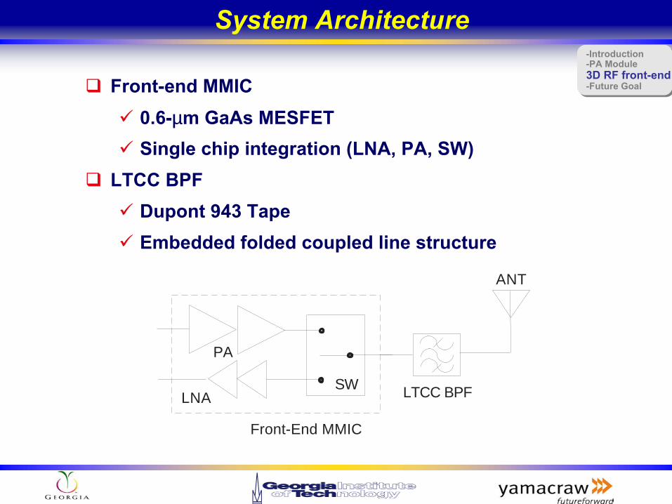
System Architecture
Front-end MMIC0.6-µm GaAs MESFETSingle chip integration (LNA, PA, SW)
LTCC BPFDupont 943 TapeEmbedded folded coupled line structure
ANT
LTCC BPF
Front-End MMIC
PA
LNASW
-Introduction-PA Module3D RF front-end-Future Goal
-Introduction-PA Module3D RF front-end-Future Goal
Page 46
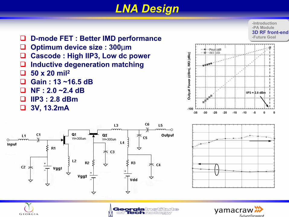
LNA Design
D-mode FET : Better IMD performanceOptimum device size : 300µmCascode : High IIP3, Low dc powerInductive degeneration matching50 x 20 mil2Gain : 13 ~16.5 dBNF : 2.0 ~2.4 dBIIP3 : 2.8 dBm3V, 13.2mA
-Introduction-PA Module3D RF front-end-Future Goal
-Introduction-PA Module3D RF front-end-Future Goal
Page 47
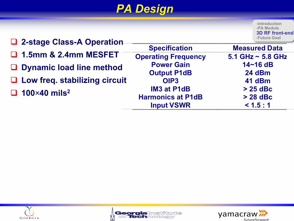
PA Design
2-stage Class-A Operation1.5mm & 2.4mm MESFETDynamic load line methodLow freq. stabilizing circuit100×40 mils2
Specification Measured DataOperating Frequency 5.1 GHz ~ 5.8 GHz
Power Gain 14~16 dBOutput P1dB 24 dBm
OIP3 41 dBmIM3 at P1dB > 25 dBc
Harmonics at P1dB > 28 dBcInput VSWR < 1.5 : 1
-Introduction-PA Module3D RF front-end-Future Goal
-Introduction-PA Module3D RF front-end-Future Goal
Page 48
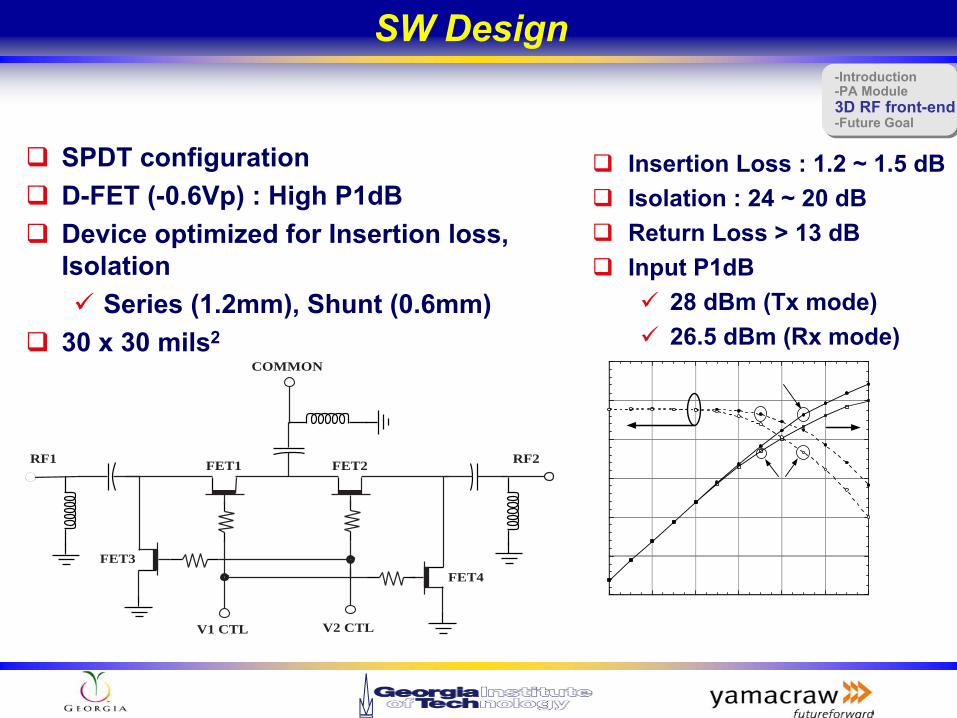
SW Design
SPDT configurationD-FET (-0.6Vp) : High P1dBDevice optimized for Insertion loss, Isolation
Series (1.2mm), Shunt (0.6mm)30 x 30 mils2
COMMON
FET1 FET2
FET3
FET4
V1 CTL
RF1 RF2
V2 CTL
Insertion Loss : 1.2 ~ 1.5 dBIsolation : 24 ~ 20 dBReturn Loss > 13 dBInput P1dB
28 dBm (Tx mode)26.5 dBm (Rx mode)
-Introduction-PA Module3D RF front-end-Future Goal
-Introduction-PA Module3D RF front-end-Future Goal
Page 49
Filter Configuration
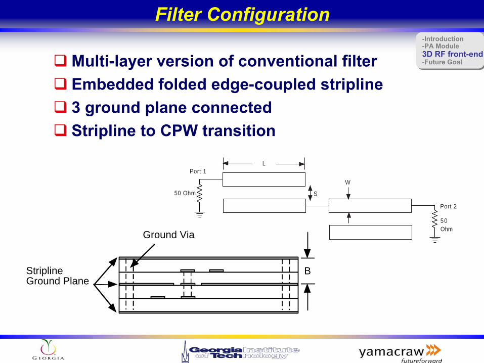
Multi-layer version of conventional filterEmbedded folded edge-coupled stripline3 ground plane connectedStripline to CPW transition
L
S
W
Port 1
Port 2
50 Ohm
50Ohm
Stripline Ground Plane
Ground Via
B
-Introduction-PA Module3D RF front-end-Future Goal
-Introduction-PA Module3D RF front-end-Future Goal
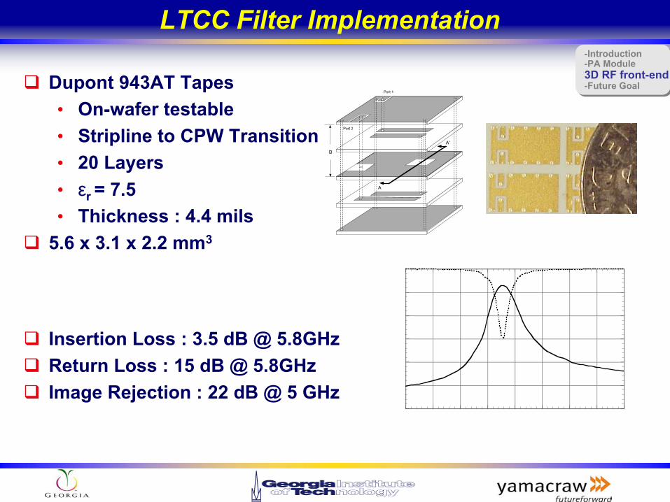
Page 50
LTCC Filter Implementation
Port 1
Port 2
B
A
A'
Insertion Loss : 3.5 dB @ 5.8GHzReturn Loss : 15 dB @ 5.8GHzImage Rejection : 22 dB @ 5 GHz
Dupont 943AT Tapes• On-wafer testable• Stripline to CPW Transition • 20 Layers• εr = 7.5• Thickness : 4.4 mils
5.6 x 3.1 x 2.2 mm3
-Introduction-PA Module3D RF front-end-Future Goal
-Introduction-PA Module3D RF front-end-Future Goal
Page 51
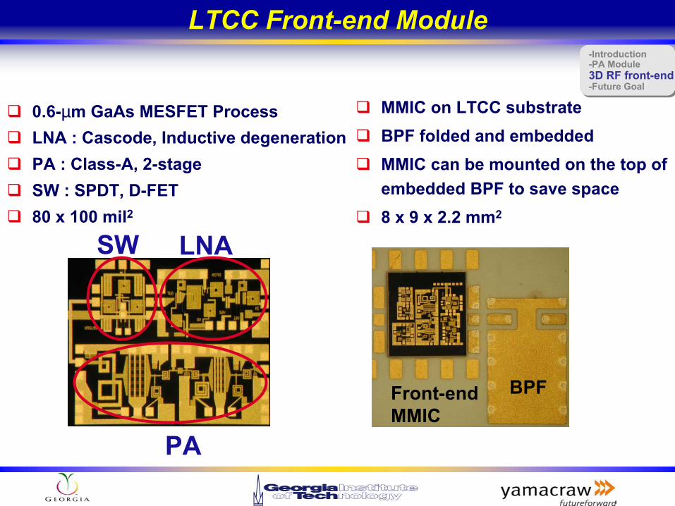
LTCC Front-end Module
MMIC on LTCC substrateBPF folded and embeddedMMIC can be mounted on the top of embedded BPF to save space8 x 9 x 2.2 mm2
BPFFront-endMMIC
SW LNA
PA
0.6-µm GaAs MESFET ProcessLNA : Cascode, Inductive degenerationPA : Class-A, 2-stageSW : SPDT, D-FET80 x 100 mil2
-Introduction-PA Module3D RF front-end-Future Goal
-Introduction-PA Module3D RF front-end-Future Goal
Page 52
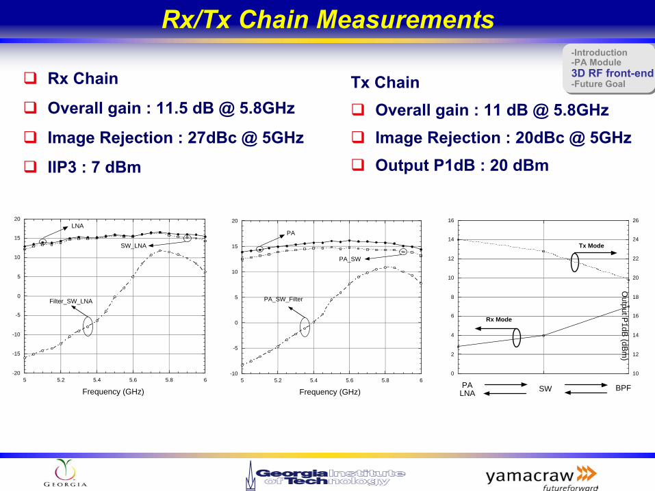
Rx/Tx Chain Measurements
Rx Chain
Overall gain : 11.5 dB @ 5.8GHz
Image Rejection : 27dBc @ 5GHz
IIP3 : 7 dBm
-20
-15
-10
-5
0
5
10
15
20
5 5.2 5.4 5.6 5.8 6
Frequency (GHz)
Filter_SW_LNA
LNA
SW_LNA
Tx ChainOverall gain : 11 dB @ 5.8GHzImage Rejection : 20dBc @ 5GHzOutput P1dB : 20 dBm
-10
-5
0
5
10
15
20
5 5.2 5.4 5.6 5.8 6
Frequency (GHz)
PA_SW_Filter
PA
PA_SW
0
2
4
6
8
10
12
14
16
10
12
14
16
18
20
22
24
26
Output P
1dB (dB
m)
PALNA SW BPF
Tx Mode
Rx Mode
-Introduction-PA Module3D RF front-end-Future Goal
-Introduction-PA Module3D RF front-end-Future Goal
Page 53
Conclusions
Highly integrated, Broadband, High Linear Front-
end Single GaAs MESFET MMIC
Embedded 3-D LTCC-based BPF
Demonstrates the feasibility of on-package
integration of RF front-end system
-Introduction-PA Module3D RF front-end-Future Goal
-Introduction-PA Module3D RF front-end-Future Goal
Page 54
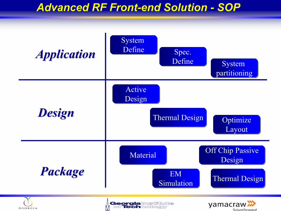
ApplicationApplication
DesignDesign
PackagePackage
System partitioning
System partitioning
Spec.DefineSpec.
Define
ActiveDesignActiveDesign
EMSimulation
EMSimulation
OptimizeLayout
OptimizeLayout
MaterialMaterial
Thermal DesignThermal Design
Advanced RF Front-end Solution - SOP
Off Chip PassiveDesign
Off Chip PassiveDesign
Thermal DesignThermal Design
System Define
System Define
Page 55
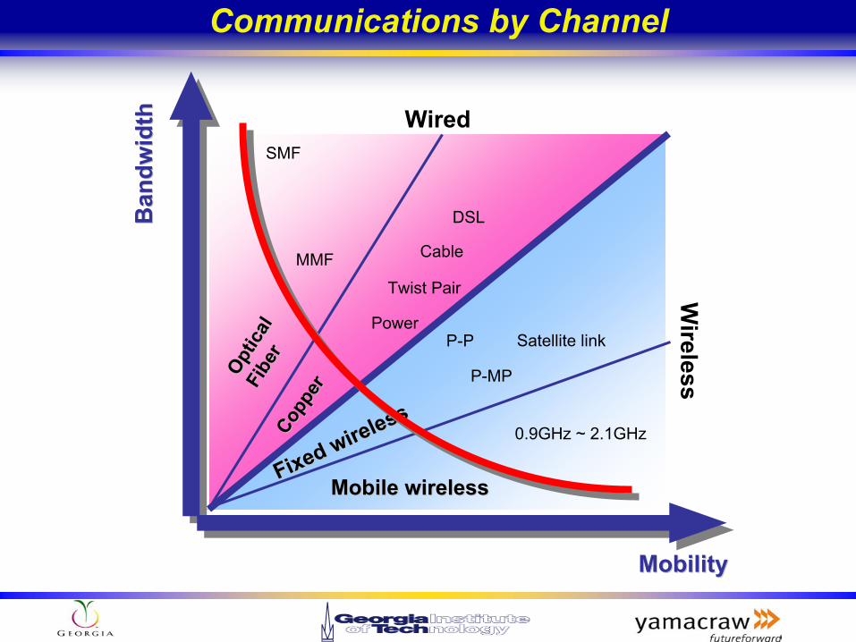
Wireless
Wired
Optica
lOpt
ical
Fibe
rFi
ber
Coppe
r
Coppe
r
Fixed wireless
Fixed wireless
Mobile wirelessMobile wireless
MobilityMobility
Ban
dwid
thB
andw
idth
SMF
MMF
DSL
Cable
Twist Pair
P-P Satellite linkPower
0.9GHz ~ 2.1GHz
P-MP
Communications by Channel
Page 56
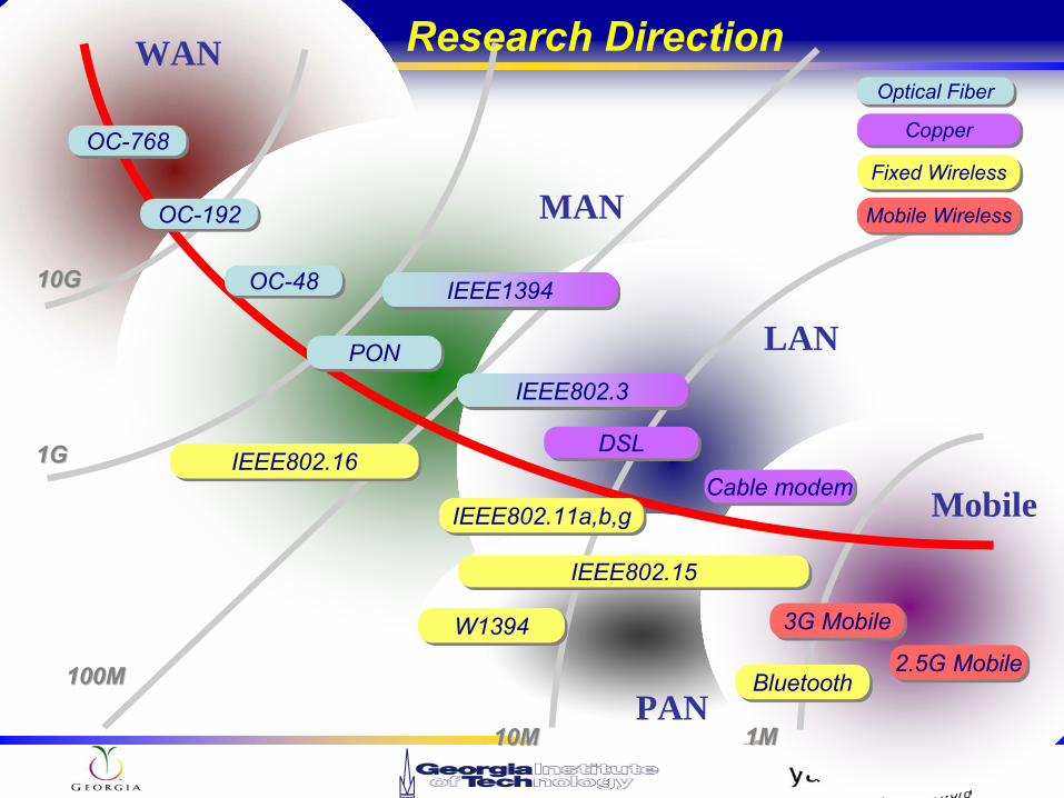
WAN
MAN
LAN
PAN
Mobile
10G10G
1G1G
100M100M
10M10M 1M1M
OC-192OC-192
OC-48OC-48
OC-768OC-768
PONPON
IEEE1394IEEE1394
DSLDSL
Cable modemCable modemIEEE802.16IEEE802.16
IEEE802.11a,b,gIEEE802.11a,b,g
IEEE802.3IEEE802.3
IEEE802.15IEEE802.15
W1394W1394
BluetoothBluetooth
3G Mobile3G Mobile
2.5G Mobile2.5G Mobile
Optical FiberOptical Fiber
CopperCopper
Fixed WirelessFixed Wireless
Mobile WirelessMobile Wireless
Research Direction
Page 57
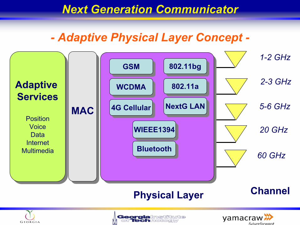
Next Generation Communicator
- Adaptive Physical Layer Concept -1-2 GHz
2-3 GHz
5-6 GHz
20 GHz
60 GHz
Channel
GSMGSM
WCDMAWCDMA
4G Cellular4G Cellular
WIEEE1394WIEEE1394
802.11bg802.11bg
BluetoothBluetooth
802.11a802.11a
NextG LANNextG LAN
Physical Layer
MACMAC
Adaptive Services
PositionVoiceData
InternetMultimedia
Adaptive Services
PositionVoiceData
InternetMultimedia
Page 58
Future Work and Research Fund
NSF New Faculty Career Award
Research Program : NSF and DARPA
NSF(Sensor and Sensor Network)
High Speed RFIC for Wireless Sensor Network
DARPA(MTO): Wide Bandgap Semiconductor Technology
High Power Microwave Circuit
DARPA(MTO): Intelligent RF Front-End
Smart RFIC Module
DARPA(MTO): VLSI Photonics, Radio-Frequency Lightwave Integrated Circuits
Optical Transceiver
Radio on Fiber
Fund from Industry : NSC, IBM, SAMSUNG, LG, CREE
Page 59
Thank you for your Attention
Deuk Hyoun Heo, Ph.D.
[email protected]
Page 60
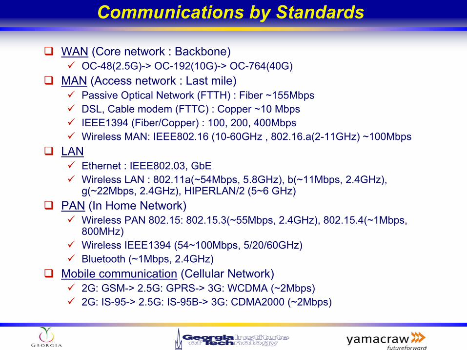
Communications by Standards
WAN (Core network : Backbone)OC-48(2.5G)-> OC-192(10G)-> OC-764(40G)
MAN (Access network : Last mile)Passive Optical Network (FTTH) : Fiber ~155MbpsDSL, Cable modem (FTTC) : Copper ~10 MbpsIEEE1394 (Fiber/Copper) : 100, 200, 400MbpsWireless MAN: IEEE802.16 (10-60GHz , 802.16.a(2-11GHz) ~100Mbps
LANEthernet : IEEE802.03, GbEWireless LAN : 802.11a(~54Mbps, 5.8GHz), b(~11Mbps, 2.4GHz), g(~22Mbps, 2.4GHz), HIPERLAN/2 (5~6 GHz)
PAN (In Home Network)Wireless PAN 802.15: 802.15.3(~55Mbps, 2.4GHz), 802.15.4(~1Mbps,800MHz)Wireless IEEE1394 (54~100Mbps, 5/20/60GHz) Bluetooth (~1Mbps, 2.4GHz)
Mobile communication (Cellular Network)2G: GSM-> 2.5G: GPRS-> 3G: WCDMA (~2Mbps)2G: IS-95-> 2.5G: IS-95B-> 3G: CDMA2000 (~2Mbps)
Page 61
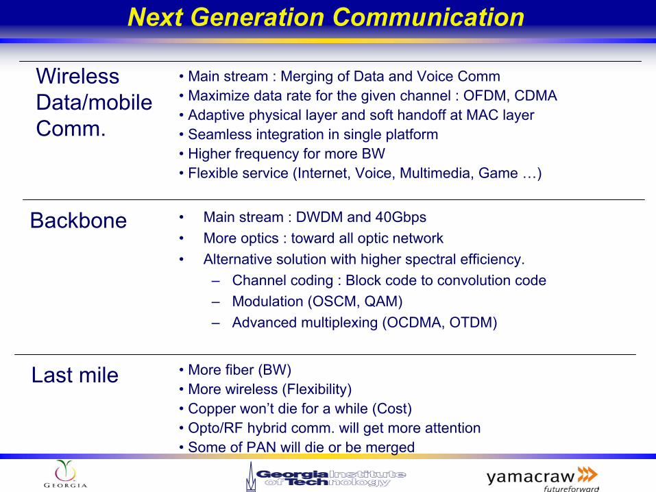
Next Generation Communication
• Main stream : DWDM and 40Gbps• More optics : toward all optic network• Alternative solution with higher spectral efficiency.
– Channel coding : Block code to convolution code – Modulation (OSCM, QAM) – Advanced multiplexing (OCDMA, OTDM)
• More fiber (BW) • More wireless (Flexibility) • Copper won’t die for a while (Cost) • Opto/RF hybrid comm. will get more attention • Some of PAN will die or be merged
• Main stream : Merging of Data and Voice Comm• Maximize data rate for the given channel : OFDM, CDMA• Adaptive physical layer and soft handoff at MAC layer• Seamless integration in single platform • Higher frequency for more BW• Flexible service (Internet, Voice, Multimedia, Game …)
Backbone
Last mile
Wireless Data/mobileComm.
Page 62
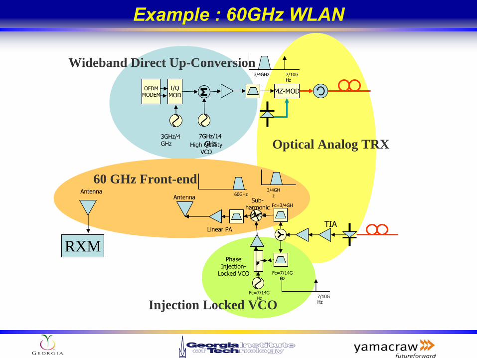
Example : 60GHz WLAN
Optical Analog TRX
Wideband Direct Up-Conversion
Injection Locked VCO
60 GHz Front-end
OFDMMODEM
I/QMOD
3GHz/4 GHz
MZ-MOD
7GHz/14 GHz
7/10GHz
3/4GHz
High Quality VCO
TIA
Phase Injection-
Locked VCO
Linear PA
Fc=7/14GHz
Fc=7/14GHz 7/10G
Hz
Fc=3/4GHz
Sub-harmonic
Mixer
3/4GHz60GHzAntenna
Antenna
RXM