EURASIP Journal on Applied Signal Processing 2005:10, 1462–1484 c 2005 Hindawi Publishing Corporation Advanced Optical Processing of Microwave Signals Beatriz Ortega Grupo de Comunicaciones Opticas, ITEAM, Universidad Polit´ ecnica de Valencia, Camino de Vera, s/n, 46022 Valencia, Spain Email: [email protected]Daniel Pastor Grupo de Comunicaciones Opticas, ITEAM, Universidad Polit´ ecnica de Valencia, Camino de Vera, s/n, 46022 Valencia, Spain Email: [email protected]Jos ´ e Mora Grupo de Comunicaciones Opticas, ITEAM, Universidad Polit´ ecnica de Valencia, Camino de Vera, s/n, 46022 Valencia, Spain Email: [email protected]Jos ´ e Capmany Grupo de Comunicaciones Opticas, ITEAM, Universidad Polit´ ecnica de Valencia, Camino de Vera, s/n, 46022 Valencia, Spain Email: [email protected]Miguel V. Andr ´ es Grupo de Semiconductores y Fibras ´ Opticas, ICMUV, Universidad de Valencia, Dr. Moliner 50, 46100 Burjassot (Valencia), Spain Email: [email protected]Received 16 April 2004; Revised 20 September 2004 The authors present a review on the recent approaches proposed to implement transversal RF filters. Different tunable transversal filters consisting of wavelength tunable optical taps and those employing the tunability of dispersive devices are presented showing their high-performance characteristics. A comprehensive review of the fundamentals and a discussion on the main limitation of these structures are also included. Keywords and phrases: microwave photonics, transversal filters, optical fibers, delay lines. 1. INTRODUCTION Over the last 25 years microwave photonics has been a discipline under constant active research because of the unique properties that photonic devices and systems bring to the generation, transport, processing, and detection of mi- crowave and millimeter wave signals [1]. The possibility of using photonic devices to implement flexible filters for microwave and radiofrequency (RF) signals with larger bandwidth is one of the applications that first at- tracted the interest of the researchers [2, 3, 4, 5, 6] since tra- ditional approaches for RF signal processing are fraught with the electronic bottleneck [2] and other sources of degradation as electromagnetic interference (EMI) and frequency depen- dent losses. An interesting approach to overcome the above limita- tions involves the use of photonics technology and espe- cially fiber and integrated photonic devices and circuits to perform the required signal processing tasks of RF signals conveyed by an optical carrier directly in the optical do- main. The discrete-time optical processing of microwave sig- nals (DOPMS) approach is shown in Figure 1. The RF-to- optical conversion is achieved by direct (or externally) mod- ulating a laser. The RF signal is conveyed by an optical car- rier and the composite signal is fed to a photonic circuit that samples the signal in the time domain, weights the samples, and combines them using optical delay lines and other pho- tonic elements. At the output(s) the resulting signal(s) are optical-to-RF converted by means of an/various optical re- ceiver(s).
Beatriz OrtegaGrupo de Comunicaciones Opticas, ITEAM, Universidad Politecnica de Valencia, Camino de Vera, s/n,46022 Valencia, SpainEmail: [email protected]
Daniel PastorGrupo de Comunicaciones Opticas, ITEAM, Universidad Politecnica de Valencia, Camino de Vera, s/n,46022 Valencia, SpainEmail: [email protected]
Jose MoraGrupo de Comunicaciones Opticas, ITEAM, Universidad Politecnica de Valencia, Camino de Vera, s/n,46022 Valencia, SpainEmail: [email protected]
Jose CapmanyGrupo de Comunicaciones Opticas, ITEAM, Universidad Politecnica de Valencia, Camino de Vera, s/n,46022 Valencia, SpainEmail: [email protected]
Miguel V. Andres
Grupo de Semiconductores y Fibras Opticas, ICMUV, Universidad de Valencia, Dr. Moliner50, 46100 Burjassot (Valencia), SpainEmail: [email protected]
Received 16 April 2004; Revised 20 September 2004
The authors present a review on the recent approaches proposed to implement transversal RF filters. Different tunable transversalfilters consisting of wavelength tunable optical taps and those employing the tunability of dispersive devices are presented showingtheir high-performance characteristics. A comprehensive review of the fundamentals and a discussion on the main limitation ofthese structures are also included.
Keywords and phrases:microwave photonics, transversal filters, optical fibers, delay lines.
1. INTRODUCTION
Over the last 25 years microwave photonics has been adiscipline under constant active research because of theunique properties that photonic devices and systems bringto the generation, transport, processing, and detection of mi-crowave and millimeter wave signals [1].
The possibility of using photonic devices to implementflexible filters for microwave and radiofrequency (RF) signalswith larger bandwidth is one of the applications that first at-tracted the interest of the researchers [2, 3, 4, 5, 6] since tra-ditional approaches for RF signal processing are fraught withthe electronic bottleneck [2] and other sources of degradationas electromagnetic interference (EMI) and frequency depen-dent losses.
An interesting approach to overcome the above limita-tions involves the use of photonics technology and espe-cially fiber and integrated photonic devices and circuits toperform the required signal processing tasks of RF signalsconveyed by an optical carrier directly in the optical do-main. The discrete-time optical processing of microwave sig-nals (DOPMS) approach is shown in Figure 1. The RF-to-optical conversion is achieved by direct (or externally) mod-ulating a laser. The RF signal is conveyed by an optical car-rier and the composite signal is fed to a photonic circuit thatsamples the signal in the time domain, weights the samples,and combines them using optical delay lines and other pho-tonic elements. At the output(s) the resulting signal(s) areoptical-to-RF converted by means of an/various optical re-ceiver(s).
The DOPMS approach is of interest, for example, inradio-over-fiber systems, both for channel rejection andchannel selection applications [7]. Another application ex-ample is for noise suppression and channel interference mit-igation in the front-end stage after the receiving antenna ofa UMTS base station prior to a highly selective SAW filter[8, 9]. Photonic filters for RF signals can also be of interest forapplications where lightweight is a prime concern, for exam-ple, analog notch filters are also needed to achieve cochan-nel interference suppression in digital satellite communica-tions systems [71]. Moreover, in moving target identification(MTI) radar systems [11] the filtering of clutter and noise(the unwanted signals) is performed using a digital notch fil-ter placed after frequency downconversion to baseband andanalog-to-digital (ADC) conversion.
Research contributions within this area extend over thelast 25 years starting with the seminal paper of Wilner andVan den Heuvel [3] who noted that the low-loss and high-modulation bandwidth of optical fibers made then an idealcandidate as a broadband delay line. Several contributionsduring the 70s addressed experimental work on DOPMS us-ing multimode fibers [4, 5]. An intensive theoretical andexperimental research work on incoherent DOPMS usingsingle-mode fiber delay lines was carried by researchers atthe University of Stanford during the period between 1980and 1990. Multiple configurations, applications, and poten-tial limitations of these structures were considered and themain results can be found summarized in [2, 6]. However,the DOPMS demonstrated serious limitations arising fromlosses and lack of reconfiguration since the technology sta-tus regarding optical fiber and integrated components was atthe time at its infancy. The advent of the optical amplifier atthe end of the 80s and the development of optical compo-nents (variable couplers, modulators, electro-optic switches)and specific purpose instrumentation fuelled the activity to-wards more flexible structures employing these components[12, 13, 14, 15, 16, 17, 18, 19, 20, 21, 22, 23, 24, 25, 26, 27,28, 29, 30, 31, 32, 33]. Nevertheless, the availability of novelcomponents, such as the fiber Bragg grating (FBG) and thearrayed waveguide grating (AWG) has opened a new perspec-tive towards the implementation of fully reconfigurable andtunable DOPMS [34, 35, 36, 37, 38, 39, 40, 41, 42, 43, 44, 45,46, 47, 48, 49, 50, 51, 52, 53, 54, 55, 56, 57, 58, 59, 60, 61, 62].
In this paper, we present the recent advances in photonicprocessing of radiofrequency signals, focusing on differentalternatives for implementing transversal filters. The outlineof this paper is as follows. In Section 2 we describe the fun-damental concepts and limitations related to the photonic RFprocessors, paying special attention to incoherent signal pro-cessing techniques. Section 3 reviews the recent advances inthe implementation of DOPMS from a structural point ofview. We discuss different alternatives for two main consoli-dated technical approaches towards the practical implemen-tation of transversal filters. The first one corresponds to tun-able transversal filters consisting of wavelength tunable op-tical taps, whereas the second one employs the tunability ofdispersive devices. In the former one, we include the effortsmade so far to overcome the limitations in incoherent filtersimposed by the positive nature of their coefficients. Finally, asummary and conclusions are presented in Section 4.
2. FUNDAMENTAL CONCEPTS AND LIMITATIONS
2.1. Fundamental concepts
Any filter implemented using DOPMS tries to provide a sys-tem function for the RF signal given by [63]
H(z−1) =
∑Nr=0 arz−r
1−∑Mk=1 bkz−k
, (1)
where z−1 represents the basic delay between samples andar , bk the filter coefficients which are implemented by op-tical components. The numerator represents the finite im-pulse part (i.e., nonrecursive or FIR) of the system function,whereas the denominator accounts for the infinite impulsepart (i.e., recursive or FIR) of the system function. N andM stand for the order of the FIR and IIR parts, respectively.If bk = 0 for all k, filter is nonrecursive and is also knownas transversal filter. Otherwise the filter is recursive and itis common to use the term recirculating delay line. Figure 2shows how (1) is implemented for anN-tap transversal inco-herent filter using a single optical source. The optical carrieris amplitude-modulated by an RF signal. Once the optical-modulated signal is tapped, each tap is differently delayedand weighted. After combining the samples, the receiver gets
1464 EURASIP Journal on Applied Signal Processing
Ω: electrical frequency
FSR ∆ΩFWHM
δ(t)
CW lasersource
e j(wot+φ(t))
RF signal
Opticalsign
altapp
ing
elem
ent
Delay line
NT
2T
T
Weight
aN
a2
a0
Opticalsign
alcombining
elem
ent
· · ·h(t): N taps
Delayed and weightedRF signals
Figure 2: Implementation layout of an N-tap incoherent transversal filter using a single optical source.
the sum of differently delayed samples in order to give thesystem response shown in the inset of Figure 2. The end-to-end (electrical) impulse response corresponding to this situ-ation can be directly derived from (1) yielding
h(t) =N∑
r=0arδ(t − rT), (2)
which convolved with the input RF signal si(t) yielding thefollowing output signal so(t):
so(t) =N∑
r=0arsi(t − rT). (3)
Similar expressions to (2) and (3) apply for IIR or recir-culating delay line filters with N →∞.
According to (2) and (3) the standard electrical/opticalimpulsive response of the optical processor is represented byan equally time-spaced (T) pulse train where pulses imple-ment the filter taps. If all the samples have the same ampli-tude, the filter is called uniform; if the samples have differ-ent amplitudes, the filter is termed as apodized or windowed[63]. The electrical frequency responseH(Ω) of such a struc-ture can be obtained by Fourier transformation of the impul-sive response (2):
H(Ω) =N∑
r=0are
− jrΩT . (4)
The above expression identifies a transfer function witha periodic spectral characteristic (see inset of Figure 2). Thefrequency period is known as the filter free spectral rangeor FSR which is inversely proportional to the time spacingT between adjacent samples in the impulse response. Theresonance full-width half-maximum is denoted as ∆ΩFWHM.
The filter selectivity is given by its quality or Q factor whichis given by
Q = FSR∆ΩFWHM
. (5)
The value of theQ factor is related to the number of sam-ples (taps) used to implement it. If the number of taps is high(greater than 10), Q factor can be approximated for uniformfilters by the number of taps Q ∼= N . This relation can beslightly corrected (Q < N) for apodized filters [63].
As shown in Figure 2, the implementation of the DOPMSrequires specific optical components to provide (a) signaltapping, (b) optical delay lines, (c) optical weights, and (d)optical signal combination, as detailed in Table 1.
Some further definitions are now introduced to completeour general description of these filters.
Coherent and incoherent operation regime
The multiple optical contributions carrying the RF signal aremixed at the detector end of the structure under two differ-ent regimes. The former regime is verified when the lightarising from each tap of the filter has a deterministic opti-cal phase relationship with the rest at the input of the pho-todetector. In this case, the optical power-to-electric currentconversion operation at the photodetector generates an in-terference term. This situation can only take place when asingle optical source is employed and its “coherence time”τc is much longer than the time delay T between adjacentsamples or taps of the optical. Under coherent regime op-eration, the optical phase of the taps plays a predominantrole in the overall time and frequency response of the pro-cessor, and filters with negative and complex coefficients canbe implemented. On the other hand, since the filter opera-tion relies on optical interferences, any slight change in thepropagation characteristics of any part of the optical proces-sor drastically affects the filter response and its properties.
Advanced Optical Processing of Microwave Signals 1465
Table 1: Components needed in a DOPMS.
Function Components
Signal tapping 2 × 2 and 1×N , N × 1 star couplersOptical signal combination 2× 2 and 1×N , N × 1 star couplers
Optical weightsVariable 2× 2 couplers, optical amplifiers (both EDFAs and SOAs),electro-optic and electroabsorption modulators
This circumstance constitutes a very serious practical lim-itation for the implementation of these filters since a verystable platform and considerable electronic feedback loopsmust be provided for successful operation. The incoherentregime is due to completely random optical phase relation-ship between the filter taps (i.e., limited source coherencetime, τc T). The interference is lost and the optical powerat the photodetector input is the sum of the optical powersof the filter samples. In this case the filter structure is freefrom environmental effects and thus is very stable and its per-formance is quite repeatable. The main drawback of this ap-proach is that filter coefficients can only be positive in princi-ple and this leads to a serious limitation of the range of trans-fer functions that can be implemented. Fortunately, there aresolutions available for the implementation of incoherent fil-ters with negative coefficients and these will be presented ina following section.
Filter tunability
This property makes reference to the possibility to tune theRF bandpass position in a sufficiently fast way. Tunability canbe achieved either in a step by step or in a continuous way,and is a key feature required for high-performance flexiblefilters. In order to tune the RF response of the filter, the FSRhas to be modified and therefore also the basic time delay Tbetween samples or taps. The techniques to produce a truetime delay can be classified as follows.
(i) Wavelength tuning of one or multiple sources combinedwith dispersive optical devices. This technique takes ad-vantage of currently available modern tunable sources.The dispersive devices can be standard fiber, high dis-persive (dispersion compensating) fiber, and linearlychirped fiber Bragg gratings (LCFBG). It can providecontinuous or step tunability at high speed, limitedby the tuning speed of the sources (depending on thetunable source technology from 100 nanoseconds togreater than 100milliseconds).
(ii) Fixed wavelength multiple sources or sliced broadbandsources combined with tunable dispersive devices. Thisapproach is based on the utilization of novel deviceswith tunable dispersion properties as special chirpedFBGs with actuators to change their dispersion prop-erties. It can provide continuous and step tunability,but in this case the time and accuracy to perform adispersion change on the Fiber device is not so wellcontrolled (100milliseconds –1 second). Discrete tun-ability can be achieved by using switched delay lines
since different paths providing different basic propa-gation delays can be chosen by means of an opticalspace switch. Only step by step tunability is allowed,and the tuning speed is limited by the switching time(1–10milliseconds).
Filter reconfiguration
This property makes reference to the possibility of chang-ing dynamically the amplitudes of the filter taps (ak, br co-efficients) to reshape its spectral response: the weighting orapodization of the amplitude of the filter taps is also a fun-damental aspect to ensure enough rejection of the avoidedbands. The uniform tap apodization (equal amplitude of thetaps) provides a rejection ratio or main-to-secondary loberatio (MSLR) that increases linearly with the number of taps.This can be insufficient for certain applications. Differentapodization functions have been demonstrated for MSLRimprovement, either by adjusting the power of the opticalsources or by controlling the attenuation/gain suffered by thetaps when they travel through the optical processor.
2.2. Limitations
DOPMS must overcome a series of potential limitationsprior to their practical realization as pointed out in previouspapers. The main limitations arise from the following.
Source coherence
The source(s) spectral characteristics must be carefully cho-sen attending to the desired working regime. While coherentoperation provides the possibility of implementing any kindof desired transfer function, these structures are very sensi-tive to environmental conditions [4]. Thus in the majorityof cases, incoherent operation is employed since the filtersare very compact and robust. Yet coherent effects can appeareven under incoherent operation. These undesirable coher-ent effects may be overcome, for instance, by the use of bir-refringent fiber delay lines [64].
Polarization
Polarization effects are mainly important under coherent op-eration [4]. However, it has been outlined and experimen-tally demonstrated that even under incoherent operation, thefilter can be sensitive to signal polarization [65]. The maincause for this apparent contradiction is that some signal sam-ples experience exactly the same delay within the filter lead-ing to coherent interference between them even if a broad-band source is employed [65]. Also, when using laser sources
1466 EURASIP Journal on Applied Signal Processing
and external modulators, care must be taken to adjust thesource polarization to that required by the modulator. Theuse of polarization preserving fiber pigtails at the modulatorinput helps to overcome this limitation.
Positive coefficients
Filters working under incoherent regime are linear in opticalintensity, thus the coefficients of their impulse responses arealways positive. This has two important implications as de-rived from the theory of positive systems [5]. The first oneand more important is that the range of transfer functionsthat can be implemented is quite limited. The second one isthat regardless of its spectral period, the transfer function al-ways has a resonance place at baseband. This is not a seriouslimitation since a DC blocking filter can be inserted at theoptical receiver output. Nevertheless, incoherent filters withnegative coefficients can be implemented by means of differ-ential detection [5, 21] and cross-gain modulation in an SOA[66] and other recently developed techniques which are fur-ther discussed in Section 4.
Limited spectral period or free spectral range
DOPMSs are periodic in spectrum since they sample the in-put signal at a time rate given by T . Thus the spectral periodor FSR is given by 1/T . If the DOPMS is fed by only one opti-cal source, then the source coherence time (which is inverselyrelated to the source linewidth) limits the maximum (mini-mum) value of the attainable FSR under incoherent (coher-ent) operation. To overcome this limitation, it has been pro-posed to feed the DOPMSs with source arrays [65].
Noise
As far as the optical source is concerned, passive DOPMSs be-have as frequency discriminators and thus convert the opti-cal source phase noise into intensity noise which materializesinto RF baseband noise at the filter output [67, 68, 69, 70, 71,72]. This conversion is dependent on the operation regime.For incoherent operation, the noise is periodic in spectrumshowing notches at zero frequency and multiples of the filterFSR. Under active operation (i.e., when incorporating opti-cal amplifiers) new RF noise sources appear as a direct con-sequence of the beating between the signal and the sponta-neous emission [71, 72]. It has been proved however, that theconverted phase noise is still the dominant noise source [72].The use of source arrays to feed the DOPMS is an attractivesolution to overcome noise limitations [58]. This is due tothe fact that signals recombining at the photodetector at dif-ferent wavelengths will generate the intensity noise centeredat the frequency resulting from the beats of the optical carri-ers. Since these have very high values, they will be filtered outby the receiver.
Reconfigurability
As defined previously, this property refers to the possibilityto dynamically change the values of ar and bk in (1). Passivestructures are incapable of this feature. Several solutions have
been proposed to overcome this limitation including the useof optical amplifiers [7, 8, 9], modulators [10, 34, 35], fibergratings, and laser arrays [56, 57, 58, 59, 60].
Tunability
As defined previously, this property refers to the possibil-ity to dynamically change the position of filter resonancesor notches. To provide tunability, it is necessary to alter thevalue of the sampling period T . Solutions that include theuse of switched fiber delay lines, fiber Bragg gratings, or othertunable tap schemes have been proposed, as will be describedbelow.
3. HIGH-PERFORMANCE INCOHERENT FILTERS
3.1. Transversal filters based on the optical tapwavelength tunability
3.1.1. Positive coefficient transversal filter
High-performance and programmable RF transversal filterscan be obtained employing both LCFBGs or fiber coils asdispersive media in combination with an array of opticalsources [56, 57, 58, 59]. The layout of the filter for a spe-cific case of a laser array of 5 elements is shown in Figure 3,although in general it is composed of N sources. The advan-tage of using a laser array to feed the delay line is twofold. Onone hand, the wavelengths of the lasers can be independentlyadjusted. Thus spectrally equally spaced signals representingRF signal samples can be fed to the fiber grating suffering dif-ferent delays, but keeping constant the incremental delay Tbetween two adjacent wavelengths emitted by the array if thedelay line is implemented bymeans of a linearly chirped fibergrating. This means, for instance, and referring to Figure 3b,that the delay between the signals at λ1 and λ2, λ3, λ4, λ5, . . . ,λN is, respectively, T , 2T , 3T , 4T , and (N − 1)T . Hence theconfiguration can act as a transversal filter, where the basicdelay is given by T . Furthermore, T can be changed by propertuning of the central wavelengths emitted by the laser array.Thus, this structure provides the potential for implementingtunable positive coefficient RF filters.
The second advantage stems from the fact that the outputpowers of the lasers can be adjusted independently at highspeed. This means that the time impulse response of the filtercan be apodized or in other words, temporal windowing canbe easily implemented and therefore the filter transfer func-tion can be reconfigured at high speed. We have experimen-tally succeeded in the demonstration of both tunability andreconfigurability. For instance, Figure 4 shows the results ofthe samples of the five-stage uniform filter where weights aregiven by a truncated Gaussian window. The upper trace inFigure 4a, shows the spectrum corresponding to the uniformfilter (i.e., unapodized) where the normalized output powersfrom the lasers in the array are [1 1 1 1 1]. The interme-diate trace corresponds to a five-stage Gaussian windowedfilter where the normalized output powers from the lasersin the array are given by [0.46 0.81 1 0.81 0.46]. Figure 4bdemonstrates the resonance tunability, increasing the reso-nance position from approximately 2GHz up to 4GHz (i.e.,
Advanced Optical Processing of Microwave Signals 1467
DFB laser
Tunable source 4
Tunable source 3
Tunable source 2
Tunable source 1
Vectorialnetworkanalyzer
5× 1coupler
Electro-opticalmodulator 2× 2
coupler Fiber grating
Adaptedterminals
(a)Reflectivity(dB)
−40
−30
−20
−10
0
1547 1548 1549 1550 1551
Wavelength (nm)
Groupdelay(ns)
0
1
2
3
4
λ1 λ2 λ3 λ4 λ5
(b)
Figure 3: Architecture of a tunable and reconfigurable RF photonic filter using a laser array and a linearly chirped fiber Bragg grating.
Frequency (GHz)
0 0.5 1 1.5 2 2.5 3 3.5 4
Amplitude
(dB)
−50−45−40−35−30−25−20−15−10−50
(a)
Frequency (GHz)
0 2 4 6 8 10
Amplitude
(dB)
−45−40
−35
−30
−25
−20
−15
−10
−5
0
(b)
Figure 4: Results of the architecture using a laser array and an LCFBG. (a) The upper trace: uniform filter (i.e., unapodized) output powersfrom the lasers in the array are [1 1 1 1 1]. The intermediate trace: five-stage Gaussian windowed filter where the normalized output powersare [0.46 0.81 1 0.81 0.46]. (b) Resonance tunability, resonance position from approximately 2GHz up to 4GHz, and details of the CSE aredemonstrated.
reducing in a factor of two the wavelength separation). In ad-dition, this figure shows the carrier suppression effect (CSE)suffered by the second resonance in this specific case of dis-persive media and wavelength spacing.
An additional advantage of employing laser arrays is thepossibility of exploiting WDM techniques for parallel signalprocessing [60]. The possibility of implementing a bank of
parallel transversal filters is feasible by extending the conceptof a single fiber-optic RF transversal filter based on multi-ple linearly chirped fiber Bragg gratings and dispersive ele-ments into the implementation of a bank of transversal fil-ters, by means of utilizing wavelength division multiplexingtechniques. This technique allows for the simultaneous pro-cessing of a single RF signal by various filters.
1468 EURASIP Journal on Applied Signal Processing
23 km fiber
LCA
EDFA
RF signal
Electro-optic modulator
90/10 coupler
SLED
OSA
Reflectedsignals
Glue
λ3
λ2
λ1
λ0
L2
UFBGs Mechanical stage
∆L (µm)0 50 100 150
λ N(nm)
1545
1546
1547
1548
1549
λ0
λ1
λ2
λ3
Figure 5: Setup of the flexible uniform FBG-based RF filter. Inset: spectral position of the reflectivity peaks (filter taps) when the fiber isstretched.
f (GHz)
0 2 4 6 8 10
H(dB)
−50
−40
−30
−20
−10
0
Figure 6: Tunability of the RF-filters. Experimental (solid line: filter1, dashed line: filter 2) and calculated (dotted line: filter 1, dash-dotted line: filter 2) filter response versus RF signal frequency withdifferent spectral spacing between taps.
A high-performance and continuously tunable positivecoefficient RF filter with larger FSR tuning range, low-costand simple tuning scheme was presented in [35]. This filterconsists of a broadband optical source, that is, a superelec-troluminescent diode, SLED, and uniform fiber Bragg grat-ings as filtering elements. This tunable approach was previ-ously demonstrated to provide a simple tunable notch filterwhere the broadband optical source was sliced by means of
only two FBGs, which can be tuned by means of a strain ap-plication stage [34]. The output light of the source is drivento the FBG through an optical circulator, and therefore, thereflected signal will be driven to the rest of the system. Theuniform FBGs are 5 cm long, written in a series configura-tion as shown in Figure 5, and they will be stretched to tunethe reflection bandwidth, initially centered at λinit. Since thecentral optical frequency, ωN , of different gratings must beequidistant [35], each grating must be stretched over a dif-ferent fiber length, LN = L/N , so the total device length isdetermined by the number of optical taps.
The device employs identical Bragg gratings whose ini-tial responses, λinitN , have been tuned by tension before glu-ing the gratings on the mechanical stage. One of the grat-ings is not glued on the stage but the others are glued overa fiber length given by N = 0, not stretched, L1 = 21 cm,L2 = 10.5 cm, and L3 = 7 cm. The inset of Figure 5 showsthe wavelength tunability of all four optical taps correspond-ing to reflected signals by the gratings when different elonga-tions are applied. The lowest wavelength is kept constant (thegrating is not stretched, so λ0 = λinit0 ) and the others show alinear behaviour, in such a way all of them are equidistant fordifferent elongations.
Figure 6 shows the measured RF-transfer function of twofilters corresponding to optical tap spectral spacing of 1.20and 0.65 nm and a fiber length of 23 km as the dispersiveelement, together with the theoretical calculation. The filterFSRs were 2.19 and 4.05GHz, respectively, although the FSRtuning range was demonstrated to be 1–6GHz.
Advanced Optical Processing of Microwave Signals 1469
Variable attenuator
Glue
ATλ0
λ3
λ2
λ1
L2To modulator
From LED 4× 4 coupler
Reflectedsignals
UFBGs Mechanical stage
Figure 7: System configuration for reconfigurable sidelobe suppression.
A similar configuration for a 4-tap filter where the grat-ings are written in a parallel configuration to achieve largesidelobe suppression by weighting the taps was also proposedin [35]. Figure 7 shows the new configuration of the grat-ings, which will show large flexibility in the implementationof the filters with the only drawback of larger optical losses,which will be compensated by the optical amplifier. The grat-ings are written in different arms of a 4 × 4 optical couplerand will be glued onto the mechanical stage over differentfiber lengths, as explained above. As known from filter the-ory [58], the shape of the transfer function of a discrete-timetransversal filter can be changed or reconfigured by chang-ing the optical power of the different taps according to anapodization function. Therefore, a decrease in the secondarysidelobes of the filter can be achieved. The optical signals cor-responding to the side taps (in our case, N = 0 and N = 3)will go through a two-input variable attenuation, which willbe varied according to the desired degree of MSLR of the RFfilter.
Figure 8 shows the measured main to sidelobe ratios ofimplemented RF filters by introducing different attenuationvalues to the optical signal taps, together with the theoreticalcurve. As an example, the intensity of the four taps of twofilters is shown in two different insets, exhibiting differentapodization profiles. The uniform intensity pattern leads usto the theoretical (and measured) limitation of 11.3 dB (seeFigure 6) and sidelobe reduction has been demonstrated inthese filters up to 25 dB.
Another interesting option is to employ AWG deviceswith high port count in order to implement source slicingwith a high number of samples [73, 74]. With this tech-nique we have recently reported a twelve-sample transversalfilter using a two-stage 1 × 40 AWG configuration shown inFigure 9. This structure has the advantage of allowing alsofilter reconfiguration if switches or variable attenuators areplaced in between the demultiplexing and the multiplexingstages.
In the structure above, the combinations of the SLED andthe erbium-doped fiber amplifier (EDFA) sources providean almost flat optical spectrum to be sliced by the coupleof AWGs. The proper channel-by-channel interconnection
AT (dB)
−3 −2 −1 0 1 2 3
MSL
R(dB)
−30
−25
−20
−15
−10
−5
P(a.u.)
P(a.u.)
λ
λ
Figure 8: Calibration curve of sidelobe suppression versus atten-uation tuning parameter. Insets: intensity of the taps in differentfilters.
between AWGs provides a certain degree of freedom to se-lect the wavelength spacing between the slices. The employedAWGs were designed for DWDM applications with 0.8 nmspacing between adjacent channels and 0.4 nm of 3 dB op-tical bandwidth. Figure 10 shows two examples of channelsinterconnections to provide different RF lobe tuning and RFlobe 3 dB bandwidth. Proper optical attenuation of the in-terconnections provide the feasibility of taps apodization toreduce the sidelobe level. Special attention must be paid tothe lowpass filtering effect arising from the combined use ofbroadband slices (0.4 nm) and large amount of dispersion,and on the other hand also the effect of the dispersion slope(S) and the large wavelength range covered must be consid-ered. This phenomenonmanifests as an amplitude reductionand an RF lobe bandwidth increasing for higher RF frequen-cies as it can be observed from results in Figure 10, and it wasextensively discussed in [74].
Another recently reported slicing technique employs afiber Bragg grating and an acoustic wave, which generatesthe optical taps when it is propagated along a uniform FBG
1470 EURASIP Journal on Applied Signal Processing
Array ofswitches orattenuators
EDFA
SLED1× 40AWG
1× 40AWG
SOA
EOM
Networkanalyser
23 km SSMFcoil
Wavelength (nm)
1540 1545 1550 1555 1560 1565
Amplitude
(dB)
−40−36−32−28−24−20
Figure 9: Spectral slicing technique employing AWGs. Inset: sliced spectrum employing twelve channels of the AWGs.
[75]. The acoustic wave creates a periodic strain perturbationthat modulates periodically the period and the refractive in-dex of the FBG. In this system, the spontaneous emission ofan EDFA around 1540 nm is used as a broadband source, theFBG is written at the neck of a symmetric tapered fiber in or-der to increase the efficiency of the acoustic interaction andthe longitudinal acoustic wave is generated by a piezoelectrictransducer driven by an RF signal and launched into the fiberusing a silica horn. It produces spectrally equispaced bandsof reflection on both sides of the original Bragg grating as wecan observe in Figure 11.
By using an SMF-28 fiber length of 46 km as a dis-persive element, two transversal filters were implementedwith the acoustic frequencies of 0.755MHz and 1.444MHz.The wavelength spacing of the optical taps were 0.11 nmand 0.22 nm, respectively, and the RF filter characteristicsare shown in Figure 12. The former one showed an FSR of6.25GHz and a 3 dB bandwidth of 1.44GHz, whereas thesecond one had an FSR of 11.5GHz and a 3 dB bandwidth of2.76GHz. The reconfigurability of the filter can be obtainedby applying different voltages to the piezoelectric transducersince different degrees of apodization of the optical taps in-tensities are achieved by controlling the acoustic power. Amain to sidelobe ratio up to 20 dB has been demonstrated.
However, in RF applications when an optical signal isused to carry several RF signals providing different services,and photonic filters are used to select one of these services,as happens in next-generation optical access networks, thereis a need for obtaining a single and very selective tunable ra-diofrequency band in sliced broadband optical source [76].The presence of a periodic transversal filter response wheredifferent RF bands are selected by the filter implies a limita-tion in the number of services carried by the same optical car-rier. Thus, a new approach to obtain single bandpass RF fil-ters is extremely interesting for their implementation in opti-
cal access networks. It is based on a broadband optical sourceand a fiber Mach-Zehnder interferometer (MZI), as shownin Figure 13. When the source optical output is transmittedby the interferometer and launched into a fiber delay line,a tunable bandpass filter is achieved showing a single band-pass frequency response, large tunability without changingthe bandwidth of the filter, and high attainable Q values.
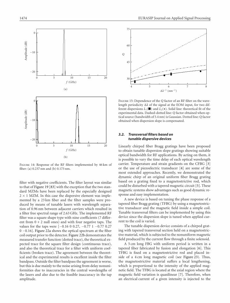
The experimental arrangement is given by the Figure 13.The spontaneous emission of an EDFA is used as broadbandoptical source, with a 3 dB bandwidth of 5.4 nm and the MZIleads to obtain different periodicities ∆ω. In this system, a46 km fiber length is used as dispersive element, and the RFfilter response shows a bandpass characteristic centered at thefrequency Ω0, that can be tuned varying the periodicity ∆ωof the interferometer Mach-Zehnder. As shown in Figure 14,periodical wavelength spacing in the interferometer ouputof 0.237 and 0.173 nm leads to bandpass filters at 5.83 and7.88GHz. A tuning range of several tens of GHz was achievedwith an MSLR lower than 20 dB and the Q maximum valueachieved was around 40.
The Q factor is plotted in Figure 15 for several RF fil-ters implemented with different wavelength periodicity ∆λof the signal at the electro-optic modulator (EOM) input,for two different dispersion values according to 23 km()and 46 km(•) length of fiber. The dashed curve plots the Qfactor that can be achieved by a Gaussian optical source of5.4 nm 3 dB bandwidth. As shown, Q value is improved byincreasing the optical source bandwidth although the influ-ence of the dispersion slope drives to a degradation of theradiofrequency response. Therefore, potential high Q valuescan be achieved by choosing the appropriated broadbandsource and reducing the dispersion slope that can be achievedby using two different fibers to compensate the dispersionslope. The dotted line shows the Q factor when the disper-sion slope is compensated.
Advanced Optical Processing of Microwave Signals 1471
Frequency (GHz)
0 2 4 6 8 10
Amplitude
(dB)
−50−45−40−35−30−25−20−15−10−50
Frequency (GHz)1.2 1.4 1.6 1.8A
mplitude
(dB)
−20−10
0
(a)
Frequency (GHz)
1 2 3 4 5 6 7 8 9 10
Amplitude
(dB)
−50−45−40−35−30−25−20−15−10−50
Wavelength (nm)1540 1550 1560
(b)
Figure 10: (a) Normalized RF amplitude for the sliced spectrum:slices from 1543.7–1561.3 nm up to a total number of twelve bands(samples), 1.6 nm apart. The RF response presents a band spacing of1.56GHz. Inset: precise measurement of the 1 passband. (b) Nor-malized RF response for 24 slices (1542.9–1561.3 nm), with 0.8 nmwavelength spacing. FSR = 3.1GHz, MSLR = 14 dB, 3 dB band-width of 125MHz, Q factor = 24.8.
3.1.2. Negative coefficient transversal filter
One of the main limitations of incoherent transversal filtersis that only positive taps are possible since the intensity isa positive magnitude. Some solutions have been reported toovercome this limitation, from the optoelectronic approachthat uses differential detection [21] to various configurationswhich use active elements to generate negative taps, that is,amplitude inversion due to gain saturation in the homoge-neously broadened gain medium of a semiconductor opticalamplifiers (SOA) [77], carrier depletion effect in a DFB laserdiode [78], cross-intensity modulation of the longitudinalmodes of an injection-locked Fabry-Perot laser diode [79].Recently, microwave filters based on wavelength conversionemploying cross-gain modulation of amplified spontaneousemission spectrum (ASE) of an SOA have been demonstrated[80]. Recently, a new low-cost approach based on passive el-ements has been proposed to generate negative taps and it isbased on filtering a broadband source with the transmissionof uniform FBGs [81].
The implemented filter is formed by a tunable laser (TL)and the signal transmitted by a uniform FBG, which is il-luminated with the ASE of an EDFA. The broadband opti-cal source has a 3 dB bandwidth of 5 nm around 1530 nm.The uniform FBG is 1 cm long with Bragg wavelength of1530.96 nm and maximum reflectivity of 8 dB. The outputlight of the FBG and the TL are driven to a 90/10 optical cou-pler. The combined signal can be monitorised by an opti-cal spectrum analyser, OSA, by using the 10% arm. The 90%arm signal is amplitude-modulated in the EOM whose RF-signal of frequency f is generated by a lightwave componentanalyser, LCA. A fiber length of 46 km will be the dispersiveelement in the filter, and finally, the transfer function of thefilter is measured in the LCA (Figure 16).
Figure 17 gives the measured and theoretically predictedfree spectral range of 2-tap RF filter versus different wave-length spacing between the central Bragg wavelength of theFBG and the TL output signal showing tunability in the 0.7–5.6GHz.
In order to show the good performance of these filterswhen various taps are added, 5-tap RF filter has been mea-sured using two FBGs and three lasers whose wavelength sep-aration is 1.16 nm (Figure 18).
Therefore, the system shows a broad tuning range and agood performance of the transversal filter.
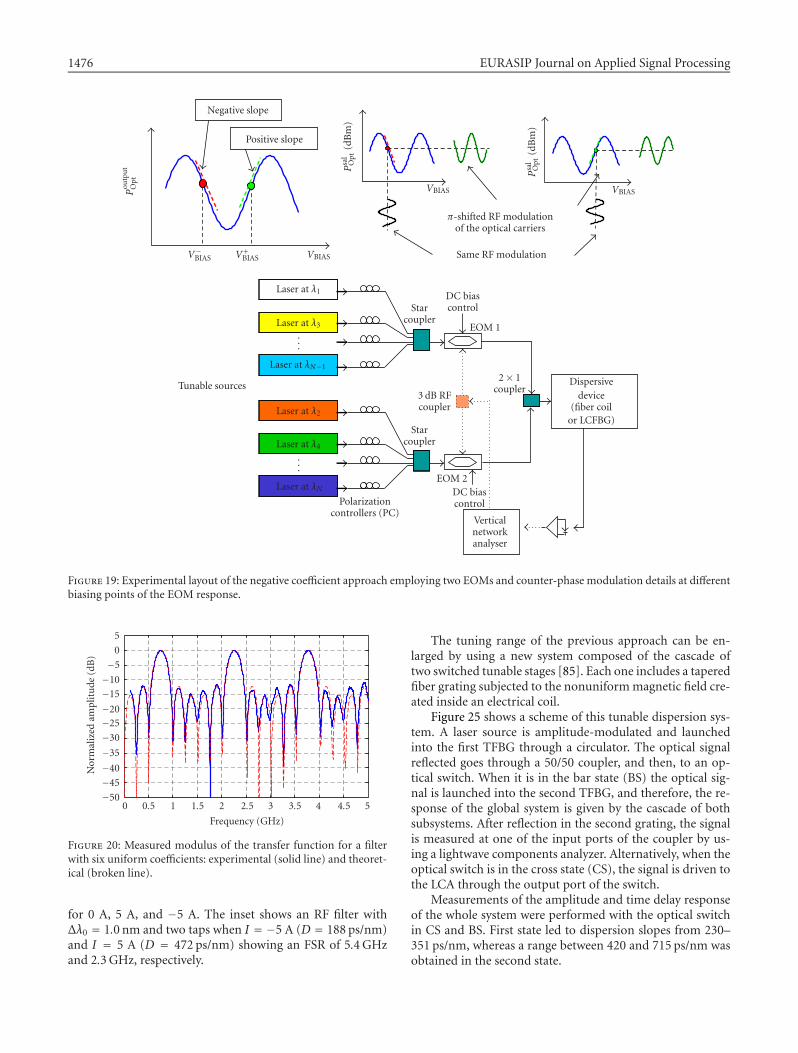
A different and promising technique also used to obtainRF filter with negative coefficients and consists of using laserarrays (like the first approach described in this section) hasbeen recently reported in [82]. It relies in the counter-phasemodulation on aMach-Zehnder external modulator (MZM)device by means of employing the linear part of the trans-fer function with positive and negative slopes. The conceptis illustrated in the upper part of Figure 19 with a simple RFmodulating source.
The upper left part of the figure depicts the typical out-put versus input optical power sinusoidal transfer functionof an MZM as a function of the applied bias voltage VBIAS.Two linear modulation regions with opposite slopes can beobserved centered at V−
BIAS and V+BIAS, respectively. As shown
in the right part of the figure, the same RF modulation signalapplied to the modulator at each of the former bias pointswill produce an optical-modulated output signal with thesame average power but where the modulating signals are180 shifted or in counter-phase. In other words they canbe considered of different signs. This principle can be em-ployed to implement RF photonic filters with negative coef-ficients if the output wavelengths from a multi-wavelengthsource (either a laser array or a sliced broadband source) areapplied to anMZM biased at eitherV+
BIAS orV−BIAS depending
on whether they are employed to implement positive or neg-ative filter samples. The output from both modulators arecombined and sent to a dispersive element (i.e., an LCFBGor a fiber coil) that implements the constant differential timedelay between the filter samples.
The feasibility of this approach has been experimentallydemonstrated with a six-sample uniform RF photonic filterwith three positive and three negative coefficients using thelaser array implementation described in [82].
1472 EURASIP Journal on Applied Signal Processing
Broadbandsource
CirculatorHorn
RF supply
Taperedfiber
Transducer
FBG
Tappingelement
LCA
Broadbandsource
Wavelength
Opticalpow
er90/10coupler 10
90 EOM
Fiber length
Wavelength
Group
delaytime
OSA
−2 −1 0 1 2λ− λB/∆λ
Reflectivity(dB)
−20
−10
0
Figure 11: Experimental setup to implement transversal filters consisting of a Bragg grating-based acousto-optic superlattice modulator.
λ (nm)
1542 1543 1544
R(dB)
−70
−60
−50
−40
(a)
f (GHz)
0 5 10 15 20
Amplitude
(dB)
45
30
15
0
(b)
λ (nm)
1542 1543 1544
R(dB)
−70
−60
−50
−40
(c)
f (GHz)
0 5 10 15 20
Amplitude
(dB)
45
30
15
0
(d)
Figure 12: (a), (c) Optical spectra and their experimental (solid lines) and (b), (d) theoretical (dashed line) transfer functions for thefrequencies (a), (b) 0.755MHz and (c), (d) 1.444MHz.
Advanced Optical Processing of Microwave Signals 1473
LCA
Broadbandoptical source
S(ω)
RF signal
Fiber length
EOM
Port 1
Port 2
Port 3
Port 450/50 couplers
∆LOSA
TMZ(ω) · S(ω)
(ω − ω0)/ω0
−0.010 −0.005 0 0.005 0.010
S(ω)
0
0.2
0.4
0.6
0.8
1
(ω− ω0)/ω0
−0.010 −0.005 0 0.005 0.010
T(ω
)
0
0.2
0.4
0.6
0.8
1
Figure 13: Schematic of the implementation of the RF single bandpass filter based on a broadband source and an MZI.
Figure 19 shows the experimental layout. An array of sixtunable lasers emitting at λ1=1546.65 nm, λ2=1548.43 nm,λ3 = 1550.11 nm, λ4 = 1551.86 nm, λ5 = 1553.47 nm, andλ6 = 1555.24 nm was selectively fed to two MZMs biasedat V+
BIAS = 0V and V−BIAS = −3.9V, respectively. Wave-
lengths λ1, λ3, and λ5 were fed to the MZM biased at V+BIAS
(positive samples) , whereas wavelengths λ2, λ4, and λ6 werefed to the MZM biased at V−
BIAS (negative samples). BothEOMs were modulated by the same RF signal, a 5 dBm si-nusoidal signal provided by an LCA. The frequency of theRF modulating signal was varied from 130MHz to 5GHz inorder to measure the transfer function characteristic of thefilter.
Figure 20 shows the measured modulus of the transferfunction for a filter with six uniform coefficients. Both theexperimental (solid line) and the theoretical (broken line) re-sults are shown for reference and comparison. As expected,the filter resonance at baseband (typical of positive coeffi-cient filters) has been eliminated, thus confirming the fea-sibility of the proposed scheme for the implementation ofnegative coefficients. Although in principle, as shown inFigure 19, two modulators are required in the transmitter, inpractice this requirement can be reduced to only one modu-lator if this device is provided with two input ports. A mainadvantage of this configuration is that there is no need to du-plicate the optical structure of the filter to implement posi-tive and negative coefficients since the taps already carry theirsign prior to being delayed. Another interesting feature isthat the sign is decoupled from any sample weighting pro-cess.
As it was anticipated, in principle two MZM devices arerequired for the previous approach, but only one MZM isrequired to incorporate 2 inputs by replacing the input Ybranch to the integrated modulator by a 2 × 2 integratedcoupler. We have reported novel results [83] using a newlydeveloped 2 × 1 MZM device fabricated by AMS (AleniaMarconi Systems) featuring the above desired characteristics.We demonstrate a filter structure that requires only this de-vice and we employ it to implement a 9-tap (positive andnegative) transversal RF photonic reconfigurable filter withsquare-type resonances.
Figure 21 shows the layout and the intensity trans-fer function of the newly developed device. The device isan LiNbO3 dual drive MZM developed for this applica-tion within the framework of the EU-funded IST-LABELSproject. As it can be observed, the input Y branch has beenreplaced by a 3 dB 2 × 2 integrated coupler. Figure 21 alsoshows the measured modulation curves for the two (input1-output) (input 2-output) input/output configurations. Asexpected, the curves for the two input/output configura-tions show a clear 180 phase shift on the two RF-modulatedoutputs with maximum dynamic range at the quadraturepoint. Note as well that the 180 phase shift on the two RF-modulated outputs is maintained regardless of the value ofthe bias voltage although the output average output powerchanges. For instance, the figure shows two cases (case (i)and case (ii)) as particular examples. The 2 × 1 MZM pre-viously described has been employed to demonstrate the op-eration concept in an experiment designed to implement, forthe first time to our knowledge, a reconfigurable square-type
1474 EURASIP Journal on Applied Signal Processing
f (GHz)
0 5 10 15 20
Amplitude
(dB)
−20
−10
0
(a)
f (GHz)
0 5 10 15 20
Amplitude
(dB)
−20
−10
0
(b)
Figure 14: Response of the RF filters implemented by 46 km offiber: (a) 0.237 nm and (b) 0.173 nm.
filter with negative coefficients. The filter layout was similarto that of Figure 19 [83] with the exception that the two stan-dard MZMs have been replaced by the especially designed2 × 1 MZM. In this case the dispersive element was imple-mented by a 23 km fiber and the filter samples were pro-duced by means of tunable lasers with wavelength separa-tion of 0.96 nm between adjacent carriers which resulted ina filter free spectral range of 2.63GHz. The implemented RFfilter was a square shape type with nine coefficients (7 differ-ent from 0 + 2 null ones) and with four negative taps. Thevalues for the taps were [−0.16 0 0.27, −0.77 1 −0.77 0.270 −0.16]. Figure 22a shows the optical spectrum at the fibercoil output prior to the detector. Figure 22b demonstrates themeasured transfer function (dotted trace), the theoretical ex-pected trace for the square filter design (continuous trace),and also the theoretical trace for a filter with uniform coef-ficients (broken trace). The agreement between the theoret-ical and the experimental results is excellent inside the filterbandpass. Outside the filter bandpass the agreement is worse,but this is due mainly to the noise arising from delay nonuni-formities due to inaccuracies in the central wavelengths ofthe lasers and also due to the feasible inaccuracy in the tapamplitude.
∆λ−1 (nm−1)4 5 6 7 8
Q
30
45
60
75
Figure 15: Dependence of the Q factor of an RF filter on the wave-length periodicity ∆λ of the signal at the EOM input, for two dif-ferent dispersions L1() and L2(•). Solid line: theoretical fit of theexperimental data. Dashed-dotted line:Q factor obtained when op-tical source (bandwidth of 5.4 nm) is Gaussian. Dotted line:Q factorobtained when dispersion slope is compensated.
3.2. Transversal filters based ontunable dispersive devices
Linearly chirped fiber Bragg gratings have been proposedto obtain tunable dispersion slope gratings showing suitableoptical bandwidth for RF applications. By acting on them, itis possible to vary the time delay of each optical wavelengthcarrier. Temperature and strain gradients on the CFBG [3]or the use of piezoelectric transducer [4] are some of themost extended approaches. Recently, we demonstrated thedynamic chirp of an original uniform fiber Bragg gratingbased on a grating fixed to a magnetostrictive rod, whichcould be disturbed with a tapered magnetic circuit [5]. Thesemagnetic systems show advantages such as good dynamic re-sponse and easy implementation.
A new device is based on tuning the phase response of atapered fiber Bragg grating (TFBG) by using a magnetostric-tive transducer and the magnetic field inside a simple coil.Tunable transversal filters can be implemented by using thisdevice since the dispersion slope is tuned when applied cur-rent to the coil is varied.
The tunable dispersion device consists of a chirped grat-ing with tapered transversal section held on a magnetostric-tive material, which is subjected to the nonuniformmagneticfield produced by the current flow through a finite solenoid.
A 5 cm long FBG with uniform period is written in atapered fiber fabricated by fusion and elongation [6]. ThisTFBG is fixed on a magnetostrictive rod and placed in-side of a 4 cm long magnetic coil (see Figure 23). Thus,the magnetostrictive material suffers a local lengthening,which is proportional to the intensity of the applied mag-netic field. The TFBG is located at the axial region where themagnetic field variation is quasilinear [7]. Therefore, whenan electrical current of a given intensity is injected to the
Advanced Optical Processing of Microwave Signals 1475
46 km fiber
LCA
RF signal
Electro-optic modulator
TL
EDFAUFBG
OSA
90/10 coupler
λ (nm)
1500 1560
−45−30−15
P(dBm)
λ (nm)
1528.5 1530 1531.5
|R(λ)|(dB)
−5
0
5
Figure 16: Setup of the RF negative-taps filter. Inset: input signal launched into EOM relative to EDFA power level.
∆λ−1 (nm−1)0.5 1 1.5 2
FSR(G
Hz)
0
2
4
6
Figure 17: Free spectral range of the RF filters dependence on thereciprocal of the wavelength spacing between taps: theoretical cal-culation (solid line) and experimental results (dots).
solenoid, the magnetic field applied to the TFBG leads to dif-ferent dispersion slopes depending on the intensity current.When no current is applied, the TFBG has a linear disper-sion due to the design of the taper profile [6]. It has a flatreflectivity and a 3 dB bandwidth of 1.58 nm.
Inset of Figure 23 shows the dispersion slope when elec-tric currents are 0 A, 3 A, and 5 A, with a 3 dB bandwidthof 1.58 nm, 2.05 nm, and 2.51 nm, respectively. Time delayslopes are achieved from 188–472 ps/nm, with a useful pass-band larger than 1 nm.
The implementation of RF filters requires N opticalcarriers, equidistant by ∆λ0/(N − 1), which are provided
f (GHz)
0 5 10
H(dB)
−60
−40
−20
λ (nm)1545 1550 1555
R(dB)
−100
10
Figure 18: Filter response versus RF signal frequency with 1.16 nmequispaced wavelength separation. Theoretical calculation (dottedline) and experimental results (solid line). Inset: spectral positionof the five taps.
by a multi-wavelength tunable laser. They are amplitude-modulated by an EOM and launched into the tunable TFBGas shown in Figure 23 [84]. The dispersion of the TFBG,D, gives the differential delay between adjacent optical taps∆τ = D · ∆λ. Because of the variation of the time delayslope of the TFBG when we apply different magnetic gradi-ents, transversal notch filters with tunable free spectral range(FSR) are measured.
Figure 24 shows the range of FSR values that can be ob-tained by using our device (shaded region).Moreover, severalfilters have been implemented by changing the number ofoptical taps and the total optical bandwidth ∆λ0 of the filter
1476 EURASIP Journal on Applied Signal Processing
Verticalnetworkanalyser
DC biascontrol
EOM 2
Starcoupler
3 dB RFcoupler
2× 1coupler
Dispersivedevice
(fiber coilor LCFBG)
DC biascontrol
EOM 1
Starcoupler
Polarizationcontrollers (PC)
...
Laser at λN
Laser at λ4
Laser at λ2
Laser at λN−1
...
Laser at λ3
Laser at λ1
Tunable sources
V−BIAS V+BIAS VBIAS
Pou
tput
Opt
Negative slope
Positive slope
Psal
Opt(dBm)
VBIAS
Psal
Opt(dBm)
VBIAS
π-shifted RF modulationof the optical carriers
Same RF modulation
Figure 19: Experimental layout of the negative coefficient approach employing two EOMs and counter-phase modulation details at differentbiasing points of the EOM response.
Frequency (GHz)
0 0.5 1 1.5 2 2.5 3 3.5 4 4.5 5
Normalized
amplitude
(dB)
−50−45−40−35−30−25−20−15−10−50
5
Figure 20: Measured modulus of the transfer function for a filterwith six uniform coefficients: experimental (solid line) and theoret-ical (broken line).
for 0 A, 5 A, and −5 A. The inset shows an RF filter with∆λ0 = 1.0 nm and two taps when I = −5 A (D = 188 ps/nm)and I = 5 A (D = 472 ps/nm) showing an FSR of 5.4GHzand 2.3GHz, respectively.
The tuning range of the previous approach can be en-larged by using a new system composed of the cascade oftwo switched tunable stages [85]. Each one includes a taperedfiber grating subjected to the nonuniformmagnetic field cre-ated inside an electrical coil.
Figure 25 shows a scheme of this tunable dispersion sys-tem. A laser source is amplitude-modulated and launchedinto the first TFBG through a circulator. The optical signalreflected goes through a 50/50 coupler, and then, to an op-tical switch. When it is in the bar state (BS) the optical sig-nal is launched into the second TFBG, and therefore, the re-sponse of the global system is given by the cascade of bothsubsystems. After reflection in the second grating, the signalis measured at one of the input ports of the coupler by us-ing a lightwave components analyzer. Alternatively, when theoptical switch is in the cross state (CS), the signal is driven tothe LCA through the output port of the switch.
Measurements of the amplitude and time delay responseof the whole system were performed with the optical switchin CS and BS. First state led to dispersion slopes from 230–351 ps/nm, whereas a range between 420 and 715 ps/nm wasobtained in the second state.
Advanced Optical Processing of Microwave Signals 1477
VBIAS
input
RF input 2
2× 1 EOM
Input 1
Input 2
Output
RF input 1
Twoopticalinputsto theMZI
Oneopticaloutput
(a)
Input 2→ output
Input 1→ output
Case (i)
Case(ii)
(+)
(−)(+)
(−)
Normalized
pow
er
(b)
Figure 21: Layout and the intensity transfer function of the newly developed device. (a) Two electrical travelling wave electrodes for dualdrive operation. (b) Optical power versus bias voltage of 2× 1 EOM.
Wavelength (nm)
1544 1546 1548 1550 1552 1554 1556
Normalized
opticalp
ower
(dB)
−70−60−50−40−30−20−10
0
Null taps(No source required)
(−) (+) (−) (+) (−) (+) (−)
(+) Positive taps
(−) Negative taps
(a)
Frequency (GHz)
0 0.5 1 1.5 2 2.5 3 3.5 4 4.5 5
Normalized
amplitude
(dB)
−35
−30
−25
−20
−15
−10
−5
0
(b)
Figure 22: (a) Optical spectrum at the detector, 9 taps (7 active and 2 null taps). (b)Measured transfer function (dotted trace), the theoreticalexpected trace (continuous trace), and the theoretical trace for a filter with uniform coefficients (broken trace).
1478 EURASIP Journal on Applied Signal Processing
LCA
Multiwavelengthsource
EOM
Magnetostrictiverod
TFBG
I
z-axis
CoilMagneticfield
λ (nm)
1544 1545 1546
τ(ps)
0200400600
Figure 23: Tunable device for RF filtering implementation based on fiber Bragg gratings subjected to nonuniform magnetic fields. Inset:time delay response when different electrical currents are applied: I = 0 (solid line), 3 (dashed line), and 5 A (dotted line).
(N − 1)/∆λ0
0 1 2 3 4 5 6 7 8
FSR(G
Hz)
0
5
10
15
f (GHz)0 5 10 15
H(dB)
−15
−10
−5
0
Dmax
Dmin
Figure 24: FSR versus number of optical taps and optical band-width of the filter for different time delay slopes. Inset: transferfunction of a tuned RF filter (solid line: D = 188 ps/nm, dashed-dotted line: D = 472 ps/nm).
To show the performance of this system, 3-tap RF fil-ters were implemented for CS and BS when different elec-trical currents are injected to the solenoid (0, 2, and 4 A).The multi-wavelength was set to emit light at three differentoptical wavelengths equispaced by 0.41 nm. Figure 26 showsthe FSR of the measured RF filters for different electricalcurrents. CS led to achieve FSRs between 7 and 10.6GHzand BS led to a tuning range from 3.5–5.8GHz. The insetof Figure 26 shows the group time delay versus wavelengthwhen no electrical current is applied to the coils. Note theincrease of the dispersion when BS was set instead of CS.
Amongst the approaches based on the concept of disper-sive adjusting and maintaining the wavelengths of the tapsfixed to obtain RF lobe tuning we can include the follow-ing RF photonic filter, although in this case other importanttechniques as spectral slicing employing uniform FBGs andfiber delay lines have been combined to perform the filter
specifications [8]. More specifically, we report a tunable pho-tonic filter for noise suppression and channel interferencemitigation in the front-end stage of a UMTS base stationprior to the highly selective SAW filter. As it has been re-ported elsewhere [9], the inclusion of such a filter can in-crease the capacity of UMTS systems. It is possible to switchthe designed filter along the twelve-channel UMTS.
The proposed configuration implements a classical FIRtransversal filter. We also employ the spectral slicing of ahigh-power broadband optical source to obtain an “equiva-lent” multi-wavelength source. The slicing is performed byan array of fiber Bragg gratings which also introduces afixed time delay between the reflected slices of the signal. Fi-nally, we employ a reconfigurable chain of dispersive mod-ules (SMF-28 fiber) to vary the time delay between the slicesand thus introduce tuneability to the filter. Figure 27 showsthe filter structure. The first block is the optical source andmodulator, where an SLED is employed as the broadband op-tical source (power of 10mW and with the 40 nm bandwidthat 1555 nm). The RF modulation of the optical signal is per-formed by means of an EOM directly over the entire SLEDspectrum. The second block consists of an array of N fiberBragg gratings written in series with certain uniform spac-ing between the gratings. This block accomplishes a doubletask: the slicing of the SLED spectrum and the introductionof the time delay ∆T between the signals reflected from thegratings. Finally, the spectral slices are fed to the third block: areconfigurable chain of dispersivemodules, where eachmod-ule employs a standard nonshifted SMF-28 fiber (the use of ahighly dispersive, e.g., dispersion compensating fiber, is alsopossible). The optical switches in the third block provide astepwise tuning of the accumulated dispersion in the block.By varying the dispersion of the block, the time delay be-tween the signals reflected from different gratings is changedand thus, tuneability of the filter RF response is achieved.
The UMTS channel filtering requires a high Q factor(about 400), since the required 3 dB passband of the filtershould be less than 5MHz and the operating frequency of the
Advanced Optical Processing of Microwave Signals 1479
LCA
Multiwavelengthsource
EOM
RFinput
Out to LCA (bar)
Y-junction
Out to LCA(cross)
Coupler
Opticalswitch TFGB
S
Coil I1
I2z-axis
z-axis
Magneticfield
(a)
Reflectivity(dBm)
−40
−30−20−10
Groupdelaytime(ns)
0.2
0.4
0.6
0.8(b)
1542 1543 1544 1545
λ (nm)
Figure 25: Schematic of the optically switched time delay line. Insets: (a) dependence of the magnetic field on the z-axis along the grating,and (b) reflectivity and time delay response of one of the chirped fiber gratings.
I (A)
0 1 2 3 4
FSR(G
Hz)
4
6
8
10
12
14
λ (nm)1543 1544
τ(ns)
0
0.5
1
CS
BS
Figure 26: Free spectral range of the RF filters versus the cur-rent intensity for cross () and bar (•) states of the switch. Inset:group delay time for cross state (351 ps/nm; solid line) and barstate (712 ps/nm; dotted line) when no current is applied to thesolenoids.
filter lies within 1920–1980MHz. Furthermore, the UMTSchannel filtering also requires the tuneability of the RF pass-band within the 12 channels allocated along the 60MHzband (between 1920 and 1980MHz). In order to achievesuch a high Q factor, the present transversal filter operatesat a higher order “resonance” of its periodic response. Inthis case, the FSR of the filter is an integer fraction of theUMTS operating frequency. The present filter has been de-signed to employ the resonance number 18. To keep the filter
tuned to the upper UMTS channel at 1977MHz when thedispersive module is “switched off,” the FSR of the filter hasbeen set to 109MHz, and the corresponding spacing betweenthe adjacent gratings has been set to 930mm. The other de-sign parameters are the total number of gratings N and thegratings reflectivity as a function of wavelength or gratingnumber. The goal of the filter design was to achieve a 3 dBbandwidth within 5-6MHz, a 1 dB bandwidth larger than3MHz, and the sidelobe rejection level larger than 40 dB. Inorder to meet the above rejection level, a normalized Gaus-sian apodization of the taps weights has been employed. Thetotal number of required gratings has been determined fromthe indicated above target bandwidth being finally fixed toN = 30. The last filter parameter to be determined was theFBG wavelength spacing that was set to 1 nm which ensuredthat the SLED optical spectrum (40 nm) was used efficiently.The 1 nm spacing has also established the length of the SMF-28 fiber required for proper switching of the operating fre-quency between the UMTS channels. We determined that5MHz steps towards lower RF frequencies require an in-crease of 23 picoseconds in the time delay ∆T which corre-sponds to about 1.35 km of SMF-28 fiber with the dispersionof 17 ps/(nm km) at 1550 nm.
The fabricated gratings have been made 1 cm long,Hamming-apodized, and had the 3 dB bandwidth of about44 pm. Each grating has been fabricated separately and thenthe gratings have been spliced to each other with the 930mmcenter-to-center spacing. Figure 28 shows the view over the17–19th and over the 18th resonance of the filter response.Each of the eight traces in either figure corresponds to a dif-ferent amount of dispersion provided by the reconfigurable
1480 EURASIP Journal on Applied Signal Processing
Dispersive mediaSSMF or DCF
DetectorL 2L 4L 8L
SLD EOM
RF in
FBG 1 FBG N
Opticalswitches
RF out
∆T Equally spaced FBGarray
Photonicfilter
SAWfilter
Front end
Figure 27: UMTS photonic filter setup.
Frequency (GHz)
1.8 1.85 1.9 1.95 2 2.05 2.1
Normalized
amplitude
(dB)
−18−16−14−12−10−8−6−4−20
(a)
Frequency (GHz)
1.93 1.94 1.95 1.96 1.97 1.98 1.99
Normalized
amplitude
(dB)
−18−16−14−12−10−8−6−4−20
(b)
Figure 28: (a) UMTS filter response over the 17–19th resonanceand (b) detail over the 18th resonance. Each of the eight traces ineither figure corresponds to a different amount of dispersion pro-vided by the reconfigurable dispersive module in different stepsfrom 0 km (higher-frequency trace) up to 10.7 km (lower-frequencytrace).
dispersive module. The introduced optical insertion loss of7 dB due to the 10.7 km long fiber and connectors (2 dB fromthe fiber and 5 dB from the connectors) has been compen-sated in the experiment by an adjustable EDFA prior to thedetector. One can see that the operation frequency of thefilter varies almost linearly versus the standard fiber length
with the slope of 3.577MHz/km (i.e., 1.39 km less or extrafiber is required for the shift of 5MHz). The rejection levelshave been obtained for each tuning position by measuringthe range from the main lobe to the highest sidelobe level in-side the rejected band, giving the 12, 13.4, 13.4, 12.8, 13, 11.4,10.9, and 10.9 dB, respectively. The smallMSLR ismainly dueto the spacing errors between the gratings, which we can alsoconclude from the fact that it is frequency dependent (e.g.,the measurements give MSLR > 24 dB at 500MHz).
4. SUMMARY AND CONCLUSIONS
In this paper, we have presented the last advances in theimplementation of photonic tunable transversal filters forRF signal processing. Following a distinction between filtersbased on wavelength tunable optical taps and others basedon the tunability of the dispersive elements that provide thetime delay between samples, last approaches have been dis-cussed.
On one hand, interesting results related to the largedegree of flexibility shown by the tunable laser array andchirped grating-based structure have been shown togetherwith other cheaper alternatives based on the slicing of broad-band optical sources either by using tunable fiber Bragg grat-ings or by using arrayed waveguide gratings. Other alter-natives include the implementation of flexible and low-costtunable transversal filters based on the generation of multi-ple taps by using an acousto-optic modulation on the fiberBragg grating.
We also introduced structures that provide high-performance filters such as the bandpass filter implementedby using a Mach-Zehnder interferometer and a broadbandoptical source and discussed the implementation of filterswith negative coefficients. These filters have been recentlydemonstrated by using two different approaches, which arealso described in this paper: either by setting different biasvoltage in an electro-optic modulator or by using fiber Bragggratings in transmission; larger flexibility in the filter re-sponse given by the implementation of negative coefficientsis demonstrated.
On the other hand, last proposals on tunable dispersivedevices based on the tunability of the chirped fiber Bragg
Advanced Optical Processing of Microwave Signals 1481
gratings characteristics have also been addressed in a singlestage or in a cascade by means of using an optical switch toincrease the tunability range of these structures. Finally, a 30-tap transversal filter implemented by using a broadband op-tical source sliced by 30 uniform fiber gratings is designed forselecting channels in a UMTS application. In this structure,the physical spacing between the gratings provide the initialresponse and the filter tunability is achieved by means of aseries of different switched fiber delay lines.
ACKNOWLEDGMENTS
The authors wish to acknowledge the EU-funded researchprojects IST-2001-37435 (LABELS) and IST-2001-32786(NEFERTITI) and the MCYT support through the Ayu-das a Parques Cientıficos and Infrestructuras FEDER pro-grammes and projects TIC2002-04344 PROFECIA and TIC2001-2969-c03-01 under which part of the work reportedhere is being carried.
REFERENCES
[1] A. J. Seeds, “Microwave photonics,” IEEE Trans. MicrowaveTheory Tech., vol. 50, no. 3, pp. 877–887, 2002.
[2] K. P. Jackson, S. A. Newton, B. Moslehi, et al., “Optical fiberdelay-line signal processing,” IEEE Trans. Microwave TheoryTech., vol. 33, no. 3, pp. 193–210, 1985.
[3] K. Wilner and A. P. Van Den Heuvel, “Fiber-optic delay linesfor microwave signal processing,” Proc. IEEE, vol. 64, no. 5,pp. 805–807, 1976.
[4] C. Chang, J. A. Cassaboom, and H. F. Taylor, “Fibre optic de-lay line devices for RF signal processing,” Electronics Letters,vol. 13, pp. 678–680, 1977.
[5] H. F. Taylor, “Fiber and integrated optical devices for signalprocessing,” in Proc. SPIE, vol. 176, pp. 17–27, 1979.
[6] K. P. Jackson and H. J. Shaw, “Fiber-optic delay-line signalprocessors,” in Optical Signal Processing, chapter 7, AcademicPress, San Diego, Calif, USA, 1987.
[7] R. A.Minasian, K. E. Alameh, and E. H.W. Chan, “Photonics-based interference mitigation filters,” IEEE Trans. MicrowaveTheory Tech., vol. 49, no. 10, pp. 1894–1899, 2001.
[8] D. Pastor, B. Ortega, J. Capmany, P.-Y. Fonjallaz, and M.Popov, “Tunable microwave photonic filter for noise and in-terference suppression in UMTS base stations,” ElectronicsLetters, vol. 40, no. 16, pp. 997–998, 2004.
[9] TSG-RANWorking Group 4, Rec. TSGR4#299048 Evaluationof up- and downlink adjacent channel performance, 3rd Gen-eration Partnership Project 3GPP, www.3gpp.org, 1999.
[10] T. Sugiyama, M. Suzuki, and S. Kubota, “An integrated inter-ference suppression scheme with adaptive equalizer for dig-ital satellite communication systems,” IEICE Transactions onCommunications, vol. E79-B, pp. 191–196, 1996.
[11] M. I. Skolnik, Introduction to Radar Systems, McGraw-Hill,New York, NY, USA, 1980.
[12] B. Moslehi, “Fibre-optic filters employing optical amplifiersto provide design flexibility,” Electronics Letters, vol. 28, no. 3,pp. 226–228, 1992.
[13] J. Capmany and J. Cascon, “Optical programmable transversalfilters using fibre amplifiers,” Electronics Letters, vol. 28, no. 13,pp. 1245–1246, 1992.
[14] V. Polo, F. Ramos, J. Martı, D. Moodie, and D. Wake, “Syn-thesis of photonic microwave filters based on external optical
modulators and wide-band chirped fiber gratings,” J. Light-wave Technol., vol. 18, no. 2, pp. 213–220, 2000.
[15] B. Moslehi, K. Chau, and J. W. Goodman, “Optical ampli-fiers and liquid-crystal shutters applied to electrically recon-figurable fiber optic signal processors,” Optical Engineering,vol. 32, pp. 974–981, 1993.
[16] J. Capmany and J. Cascon, “Direct form I fiber-optic discrete-time signal processors using optical amplifiers and embeddedMach-Zehnder structures,” IEEE Photon. Technol. Lett., vol. 5,no. 7, pp. 842–844, 1993.
[17] M. C. Vazquez, R. Civera, M. Lopez-Amo, and M. A. Muriel,“Analysis of double-parallel amplified recirculating optical de-lay lines,” Applied Optics, vol. 33, no. 6, pp. 1015–1021, 1994.
[18] A. Ho-Quoc and S. Tedjini, “Experimental investigation onthe optical unbalanced Mach-Zehnder interferometers as mi-crowave filters,” IEEE Microwave Guided Wave Lett., vol. 4,no. 6, pp. 183–185, 1994.
[19] D. Pastor, S. Sales, J. Capmany, J.Martı, and J. Cascon, “Ampli-fied double-coupler fiber-optic delay line filter,” IEEE Photon.Technol. Lett., vol. 7, no. 1, pp. 75–77, 1995.
[20] J. Capmany, J. Cascon, J. L. Martın, and J. Martı, “Fibre-opticdelay line filter synthesis using a modified PADE method,”Electronics Letters, vol. 31, no. 6, pp. 479–480, 1995.
[21] S. Sales, J. Capmany, J. Martı, and D. Pastor, “Experimentaldemonstration of fibre-optic delay line filters with negativecoefficients,” Electronics Letters, vol. 31, no. 13, pp. 1095–1096,1995.
[22] S. Sales, J. Capmany, D. Pastor, and J. Martı, “Fiber-optic delayline filters employing fiber loops: signal and noise analysis andexperimental characterization,” Journal of the Optical Societyof America A, vol. 12, no. 10, pp. 2129–2135, 1995.
[23] J. Capmany, J. Cascon, J. L. Martın, S. Sales, D. Pastor, and J.Martı, “Synthesis of Fiber-optic delay line filters,” J. LightwaveTechnol., vol. 13, no. 10, pp. 2003–2012, 1995.
[24] E. C. Heyde and R. A. Minasian, “A solution to the synthesisproblem of recirculating optical delay line filters,” IEEE Pho-ton. Technol. Lett., vol. 6, no. 7, pp. 833–835, 1994.
[25] S. Sales, J. Capmany, J. Martı, and D. Pastor, “Novel and sig-nificant results on the nonrecirculating delay line with a fibreloop,” IEEE Photon. Technol. Lett., vol. 7, no. 12, pp. 1439–1440, 1995.
[26] D. Norton, S. Johns, C. Keefer, and R. Soref, “Tunable mi-crowave filtering using high dispersion fiber time delays,”IEEE Photon. Technol. Lett., vol. 6, no. 7, pp. 831–832, 1994.
[27] M. E. Frankel and R. D. Esman, “Fiber-optic tunable mi-crowave transversal filter,” IEEE Photon. Technol. Lett., vol. 7,no. 2, pp. 191–193, 1995.
[28] S. Yegnanarayanan, P. D. Trinh, and B. Jalali, “Recirculatingphotonic filter: a wavelength-selective time delay for phased-array antennas andwavelength code-divisionmultiple access,”Optics Letters, vol. 21, no. 10, pp. 740–742, 1996.
[29] F. Coppinger, S. Yegnanarayanan, P. D. Trinh, B. Jalali, andI. L. Newberg, “Nonrecursive tunable photonic filter usingwavelength-selective true time delay,” IEEE Photon. Technol.Lett., vol. 8, no. 9, pp. 1214–1216, 1996.
[30] F. Coppinger, S. Yegnanarayanan, P. D. Trinh, and B. Jalali,“Continuosly tunable photonic radio-frequency notch fil-ter,” IEEE Photon. Technol. Lett., vol. 9, no. 3, pp. 339–341,1997.
[31] N. You and R. A. Minasian, “A novel tunable microwave opti-cal notch filter,” IEEE Trans. Microwave Theory Tech., vol. 49,no. 10, pp. 2002–2005, 2001.
[32] A. P. Foord, P. A. Davies, and P. A. Greenhalgh, “Synthe-sis of microwave and millimetre-wave filters using opticalspectrum-slicing,” Electronics Letters, vol. 32, no. 4, pp. 390–391, 1996.
1482 EURASIP Journal on Applied Signal Processing
[33] J. Capmany, D. Pastor, and B. Ortega, “Fibre-optic microwaveand millimetre wave filter with high density sampling andvery high sidelobe supression using subnanometre opticalspectrum slicing,” Electronics Letters, vol. 35, no. 6, pp. 494–496, 1999.
[34] D. Pastor, J. Capmany, and B. Ortega, “Broad-band tunablemicrowave transversal notch filter based on tunable uniformfiber Bragg gratings as slicing filters,” IEEE Photon. Technol.Lett., vol. 13, no. 7, pp. 726–728, 2001.
[35] J. Mora, B. Ortega, J. Capmany, et al., “Automatic tunable andreconfigurable fiberoptic microwave filters based on a broad-band optical source sliced by uniform fiber Bragg gratings,”Optics Express, vol. 10, no. 22, pp. 1291–1298, 2002.
[36] S. Yegnanarayanan, F. Coppinger, P. D. Trinh, and B. Jalali,“Microwave transversal filter based on spectral tapping ofbroadband light in an integrated waveguide prism, P CWF55,”in Conference on Lasers and Electro-Optics (CLEO ’97), vol. 11,pp. 259–259, Baltimore, Md, USA, May 1997.
[37] D. Pastor, B. Ortega, J. Capmany, S. Sales, A. Martinez, andP. Munoz, “Flexible and tunable microwave filters based onarrayed waveguide gratings,” in Proc. IEEE International Topi-cal Meeting on Microwave Photonics (MWP ’02), pp. 189–192,November 2002.
[38] T. A. Yost, P. R. Herczfeld, A. Rosen, and S. Singh, “Hybridtransversal filter utilizing MMIC and optical fiber delay lines,”IEEE Microwave Guided Wave Lett., vol. 5, no. 9, pp. 287–289,1995.
[39] W. Zhang and J. A. R. Williams, “Fibre optic bandpasstransversal filter employing fibre grating arrays,” ElectronicsLetters, vol. 35, no. 12, pp. 1010–1011, 1999.
[40] D. Pastor, J. Capmany, S. Sales, P. Munoz, and B. Ortega, “Re-configurable fiber-optic-based RF filters using current injec-tion in multimode lasers,” IEEE Photon. Technol. Lett., vol. 13,no. 11, pp. 1224–1226, 2001.
[41] G. A. Ball, W. H. Glenn, and W. W. Morey, “Programmablefiber optic delay line,” IEEE Photon. Technol. Lett., vol. 6, no. 6,pp. 741–743, 1994.
[42] D. B. Hunter, R. A. Minasian, and P. A. Krug, “Tunable op-tical transversal filter based on chirped gratings,” ElectronicsLetters, vol. 31, no. 25, pp. 2205–2207, 1995.
[43] D. B. Hunter and R. A. Minasian, “Microwave optical filtersusing in-fiber Bragg grating arrays,” IEEE Microwave GuidedWave Lett., vol. 6, no. 2, pp. 103–105, 1996.
[44] W. Zhang and J. A. R. Williams, “Fibre optic bandpasstransversal filter employing fibre grating arrays,” ElectronicsLetters, vol. 35, no. 12, pp. 1010–1011, 1999.
[45] G. Yu, W. Zhang, and J. A. R. Williams, “High-performancemicrowave transversal filter using fiber Bragg grating arrays,”IEEE Photon. Technol. Lett., vol. 12, no. 9, pp. 1183–1185,2000.
[46] W. Zhang, J. A. R. Williams, and I. Bennion, “Polarizationsynthesized optical transversal filter employing high birefrin-gence fiber gratings,” IEEE Photon. Technol. Lett., vol. 13,no. 5, pp. 523–525, 2001.
[47] W. Zhang, G. Yu, and J. A. R. Williams, “Tap multiplexed fi-bre grating-based optical tranversal filter,” Electronics Letters,vol. 36, no. 20, pp. 1708–1710, 2000.
[48] W. Zhang, J. A. R. Williams, and I. Bennion, “Optical fiber re-circulating delay line incorporating a fiber grating array,” IEEEMicrowave and Wireless Components Letters, vol. 11, no. 5,pp. 217–219, 2001.
[49] D. B. Hunter and R. A. Minasian, “Microwave optical filtersbased on a fibre Bragg grating in a loop structure,” in Proc.International Topical Meeting on Microwave Photonics (MWP’96), pp. 273–276, Kyoto, Japan, December 1996.
[50] D. B. Hunter and R. A. Minasian, “Photonic signal process-ing of microwave signals using active-fiber Bragg-grating-pairstructure,” IEEE Trans. Microwave Theory Tech., vol. 45, no. 8,pp. 1463–1466, 1997.
[51] N. You and R. A. Minasian, “A novel high-Q optical mi-crowave processor using hybrid delay line filters,” IEEE Trans.Microwave Theory Tech., vol. 47, no. 7, pp. 1304–1308, 1999.
[52] R. A.Minasian, K. E. Alameh, and E. H.W. Chan, “Photonics-based interference mitigation filters,” IEEE Trans. MicrowaveTheory Tech., vol. 49, no. 10, pp. 1894–1899, 2001.
[53] E. H. W. Chan, K. E. Alameh, and R. A. Minasian, “Photonicbandpass filters with high skirt selectivity and stopband atten-uation,” J. Lightwave Technol., vol. 20, no. 11, pp. 1962–1967,2002.
[54] W. Zhang, J. A. R. Williams, L. A. Everall, and I. Bennion,“Fibre-optic radio frequency notch filter with linear and con-tinous tuning by using a chirped fibre grating,” Electronics Let-ters, vol. 34, no. 18, pp. 1770–1772, 1998.
[55] D. B. Hunter and R. A. Minasian, “Tunable microwave fiber-optic bandpass filters,” IEEE Photon. Technol. Lett., vol. 11,no. 7, pp. 874–876, 1999.
[56] D. Pastor and J. Capmany, “Fiber optic tunable transversal fil-ter using laser array and linearly chirped fibre grating,” Elec-tronics Letters, vol. 34, no. 17, pp. 1684–1685, 1998.
[57] J. Capmany, D. Pastor, and B. Ortega, “Experimental demon-stration of tunability and transfer function reconfiguration infibre-optic microwave filters composed of linearly chirped fi-bre grating fed by a laser array,” Electronics Letters, vol. 34,no. 23, pp. 2262–2264, 1998.
[58] J. Capmany, D. Pastor, and B. Ortega, “New and flexible fiber-optic delay-line filters using chirped Bragg gratings and laserarrays,” IEEE Trans. Microwave Theory Tech., vol. 47, no. 7,pp. 1321–1326, 1999.
[59] D. Pastor, J. Capmany, and B. Ortega, “Efficient sidelobesuppression by source power apodisation on fibre-optic mi-crowave filters composed of linearly chirped fibre grating bylaser array,” Electronics Letters, vol. 35, no. 8, pp. 640–642,1999.
[60] D. Pastor, J. Capmany, and B. Ortega, “Experimental demon-stration of parallel fiber-optic-based RF filtering using WDMtechniques,” IEEE Photon. Technol. Lett., vol. 12, no. 1, pp. 77–78, 2000.
[61] N. You and R. A. Minasian, “Synthesis ofWDM grating-basedoptical microwave filter with arbitrary impulse response,” inProc. International Topical Meeting on Microwave Photonics(MWP ’99), vol. 1, pp. 223–226, Melbourne, Victoria, Aus-tralia, November 1999.
[62] J. Mora, B. Ortega, M. V. Andres, et al., “Dynamic opticaltransversal filters based on a tunable dispersion fiber Bragggrating,” in Proc. International Topical Meeting on MicrowavePhotonics (MWP ’01), pp. 203–206, Long Beach, Calif, USA,January 2001.
[63] A. V. Oppenheim, R.W. Schaffer, and J. R. Buck,Discrete TimeSignal Processing, Prentice Hall, Englewood Cliffs, NJ, USA,1996.
[64] W. Zhang, J. A. R. Williams, and I. Bennion, “Optical fibre de-lay line filter free of limitation imposed by optical coherence,”Electronics Letters, vol. 35, no. 24, pp. 2133–2134, 1999.
[65] A. Ho-Quoc, S. Tedjini, and A. Hilt, “Optical polarization ef-fect in discrete time fiber-optic structures for microwave sig-nal processing,” in Proc. IEEEMTT-S International MicrowaveSymposium Digest, vol. 2, pp. 907–910, San Francisco, Calif,USA, June 1996.
[66] F. Coppinger, S. Yegnanarayanan, P. D. Trinh, and B. Jalali,“All-optical incoherent negative taps for photonic signal pro-cessing,” Electronics Letters, vol. 33, no. 11, pp. 973–975, 1997.
Advanced Optical Processing of Microwave Signals 1483
[67] M. Tur and B. Moslehi, “Laser phase noise effects in fiber-optic signal processors with recirculating loops,” Optics Let-ters, vol. 8, no. 4, pp. 229–231, 1983.
[68] M. Tur, B. Moslehi, and J. W. Goodman, “Theory of laserphase noise in recirculating fiber optic delay lines,” J. Light-wave Technol., vol. 3, no. 1, pp. 20–30, 1985.
[69] M. Tur and A. Arie, “Phase induced intensity noise in con-catenated fiber-optic delay lines,” J. Lightwave Technol., vol. 6,no. 1, pp. 120–130, 1988.
[70] B. Moslehi, “Analysis of optical phase noise in fiber-optic sys-tems employing a laser source with arbitrary coherence time,”J. Lightwave Technol., vol. 4, no. 9, pp. 1334–1351, 1986.
[71] J. T. Kringlebotn and K. Blotekjaer, “Noise analysis of an am-plified fiber-optic recirculating-ring delay line,” J. LightwaveTechnol., vol. 12, no. 3, pp. 573–582, 1994.
[72] J. Capmany, “Investigation on phase-induced intensity noisein amplified fibre-optic recirculating delay line,” ElectronicsLetters, vol. 29, no. 4, pp. 346–347, 1993.
[73] D. Pastor, B. Ortega, J. Capmany, S. Sales, A. Martinez, andP. Munoz, “Flexible and tunable microwave filters based onarrayed waveguide gratings,” in Proc. IEEE International Topi-cal Meeting on Microwave Photonics (MWP ’02), pp. 189–192,Long Beach, Calif, USA, November 2002.
[74] D. Pastor, B. Ortega, J. Capmany, S. Sales, A. Martinez, andP. Munoz, “Optical microwave filter based on spectral slicingby use of arrayed waveguide gratings,” Optics Letters, vol. 28,no. 19, pp. 1802–1804, 2003.
[75] M. Delgado-Pinar, J. Mora, B. Ortega, A. Dıez, M. V. Andres,and J. Capmany, “Tunable and reconfigurable microwavefilter by use of a Bragg-grating-based acousto-optic super-lattice modulator,” Optics Letters, vol. 30, no. 1, pp. 8–10,2005.
[76] J. Mora, B. Ortega, M. V. Andres, J. Capmany, A. Dıez, andD. Pastor, “A single bandpass tunable photonic transversal fil-ter based on a broadband optical source and a Mach-Zehnderinterferometer,” in Proc. IEEE International Topical Meetingon Microwave Photonics (MWP ’03), pp. 251–254, Budapest,Hungary, September 2003.
[77] F. Coppinger, S. Yegnanarayanan, P. D. Trinh, and B. Jalali,“All-optical RF filter using amplitude inversion in a semicon-ductor optical amplifier,” IEEE Trans. Microwave Theory Tech.,vol. 45, no. 8, pp. 1473–1477, 1997.
[78] S. Li, K. S. Chiang, A. Gambling, Y. Liu, L. Zhang, and I.Bennion, “A novel tunable all-optical incoherent negative-tap fiber-optic transversal filter based on a DFB laser diodeand fiber Bragg gratings,” IEEE Photon. Technol. Lett., vol. 12,no. 9, pp. 1207–1209, 2000.
[79] X. Wang and K. T. Chan, “Tunable all-optical incoherentbipolar delay-line filter using injection-locked Fabry-Perotlaser and fibre Bragg gratings,” Electronics Letters, vol. 36,no. 24, pp. 2001–2003, 2000.
[80] Y. Xiaoke, F. Wei, N. J. Hong, and L. Chao, “Tunable mi-crowave filter design using wavelength conversion techniqueand high dispersion time delays,” IEEE Photon. Technol. Lett.,vol. 13, no. 8, pp. 857–859, 2001.
[81] J. Mora, M. V. Andres, J. L. Cruz, et al., “Tunable all-opticalnegative multi-tap microwave filters based on uniform fiberBragg gratings,” Optics Letters, vol. 28, no. 15, pp. 1308–1310,2003.
[82] J. Capmany, D. Pastor, A. Martinez, B. Ortega, and S. Sales,“Microwave photonic filters with negative coefficients basedon phase inversion in an electro-optic modulator,” Optics Let-ters, vol. 28, no. 16, pp. 1415–1417, 2003.
[83] D. Pastor, J. Capmany, B. Ortega, A. Martinez, L. Pierno, andM. Varasi, “Reconfigurable RF photonic filter with negativecoefficients and flat-top resonances using phase inversion in
a newly designed 2 × 1 integrated Mach-Zehnder modula-tor,” IEEE Photon. Technol. Lett., vol. 16, no. 9, pp. 2126–2128,2004.
[84] J. Mora, B. Ortega, M. V. Andres, et al., “Tunable dispersiondevice based on a tapered fiber Bragg grating and nonuniformmagnetic fields,” IEEE Photon. Technol. Lett., vol. 15, no. 7,pp. 951–953, 2003.
[85] J. Mora, B. Ortega, A. Dıez, et al., “Highly tunable opticallyswitched time delay line for transversal filtering,” ElectronicsLetters, vol. 39, no. 25, pp. 1799–1800, 2003.
Beatriz Ortega was born in Valencia, Spain,in 1972. She received the M.S. degree inphysics in 1995 from the Universidad deValencia, and the Ph.D. degree in telecom-munications engineering in 1999 from theUniversidad Politecnica de Valencia. Shejoined the Departamento de Comunica-ciones, Universidad Politecnica de Valencia,in 1996, where she was engaged with theOptical Communications Group and herresearch was mainly in the field of fiber gratings. From 1997 to1998, she joined the Optoelectronics Research Centre, Universityof Southampton, United Kingdom, where she was involved in sev-eral projects developing new add-drop filters or twin-core fiber-based filters. She has published more than 60 papers and con-ference contributions in fiber Bragg gratings, microwave photon-ics, and fiber filters. Currently, she is an Associate Lecturer at theTelecommunications Engineering Faculty and her main interestsinclude fiber gratings applications, optical delay lines, and opticalnetworks.
Daniel Pastor was born in Elda, Spain, onNovember 5, 1969. He received the Inge-niero de Telecomunicacion degree in 1993from the Universidad Politecnica de Valen-cia, and the Doctor Ingeniero de Telecomu-nicacion (Ph.D.) degree in 1996 from theUniversidad Politecnica de Valencia, Spain.He joined the Departamento de Comunica-ciones, Universidad Politecnica de Valencia,in 1993, where he was engaged with the Op-tical Communications Group. From 1994 to 1998 he was a Lec-turer at the Telecommunications Engineering Faculty and he be-came an Associate Professor in 1999. He has published over 45papers and conference contributions in the fields of optical delay-line filters, fiber Bragg gratings, microwave photonics, and WDMand SCM lightwave systems. His current technical interests includemicrowave photonics, fiber Bragg grating applications, and WDMnetworks.
Jose Mora was born in Torrent, Valencia,Spain, in 1976. He received the Licenciadoen Fısica degree in 1999 from the Universi-dad de Valencia, Spain. From 1999 to 2004he has served as Ph.D. student in the Depar-tamento de Fısica Aplicada, Universidad deValencia. Currently, he is a Researcher in theOptical Communications Group, Universi-dad Politecnica de Valencia. His research ac-tivities are focused on the use of fiber Bragggratings in fields such as sensor applications and telecommunica-tion systems.
1484 EURASIP Journal on Applied Signal Processing
Jose Capmany was born in Madrid, Spain,in 1962. He received the Ingeniero de Tele-comunicacion degree from the UniversidadPolitecnica de Madrid in 1987. From 1988to 1991, he worked as a Research Assistant atthe Departamento de Tecnologıa Fotonica,Universidad Politecnica de Madrid, wherehe received the Ph.D. degree in 1991. In1991 he moved to the Departamento de Co-municaciones, Universidad Politecnica deValencia, where he started the activities on optical communica-tions and photonics, founding the Optical Communications Group(www.gco.upv.es). He has been an Associate Professor from 1992 to1996, and Full Professor in optical communications, systems, andnetworks since 1996. Since 2002, he has also been the Director ofthe IMCO2 Research Institute, Universidad Politecnica de Valencia.His research activities and interests cover a wide range of subjectsrelated to optical communications including optical signal process-ing, fiber resonators, fiber gratings, RF filters, SCM, WDM, andCDMA transmission, wavelength conversion, and optical bistabil-ity. He has published over 200 papers in international refereed jour-nals and conferences and has been a Member of the Technical Pro-grammeCommittees of the European Conference onOptical Com-munications (ECOC), the Optical Fiber Conference (OFC), the In-tegrated Optics and Optical Communications Conference (IOOC),CLEO Europe.
Miguel V. Andres was born in Valencia,Spain, in 1957. He received the Licenciadoen Fısica degree in 1979, and the Doctoren Fısica (Ph.D.) degree in 1985, both fromthe Universidad de Valencia, Spain. From1983 he has served successively as AssistantProfessor and Lecturer in the Departamentode Fısica Aplicada, Universidad de Valen-cia. From 1984 to 1987 he was visiting forseveral periods the Department of Physics,University of Surrey, UK, as a Research Fellow. Until 1984 he wasengaged in research on microwave surface waveguides. His cur-rent research interests include waveguide theory (inhomogeneouswaveguides and microstructured optical fibres) and optical fiberdevices and systems for microwave photonics and sensor applica-tions (optical fiber interferometers, evanescent field devices basedon optical fiber tapers, in-fiber Bragg gratings, and photonic crystalfibres). Dr. M. V. Andres is a Member of IEEE, OSA, and IOP.