Advances in Nanotechnology/Nanomedicine Advances in Nanotechnology/Nanomedicine Charles E. May Center for Nanoscale Science and Engineering Center for Nanoscale Science and Engineering University of Kentucky, Lexington, Kentucky
Transcript
Advances in Nanotechnology/NanomedicineAdvances in Nanotechnology/Nanomedicine
Charles E. MayCenter for Nanoscale Science and EngineeringCenter for Nanoscale Science and Engineering
University of Kentucky, Lexington, Kentucky
What is Nanotechnology?
• The Science of and Research and technology development at the atomic, molecular or macromolecular levels, in the length scale of 1 100 nanometersscale of 1 - 100 nanometers.
• Creating and using structures, devices and systems that have novel properties and functions because of the nanoscale.
• Ability to control processes at a few nm-range for advanced material processing and manufacturing.
• The deployment of chemicals, drugs, sealants that are fully or partially made up of nanoscale materials
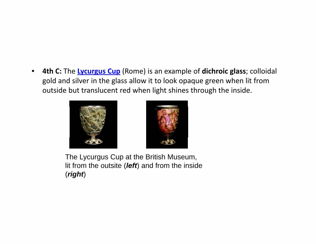
• 4th C: The Lycurgus Cup (Rome) is an example of dichroic glass; colloidal gold and silver in the glass allow it to look opaque green when lit from outside but translucent red when light shines through the inside.
The Lycurgus Cup at the British Museum, lit from the outsite (left) and from the inside ( )(right)
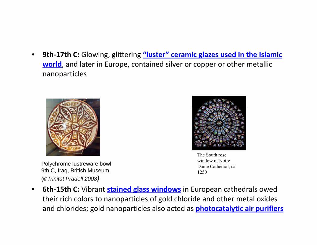
• 9th‐17th C: Glowing, glittering “luster” ceramic glazes used in the Islamic world, and later in Europe, contained silver or copper or other metallic nanoparticlesnanoparticles
Polychrome lustreware bowl, 9th C I B iti h M
The South rose window of Notre Dame Cathedral, ca
• 6th‐15th C: Vibrant stained glass windows in European cathedrals owed their rich colors to nanoparticles of gold chloride and other metal oxides
their rich colors to nanoparticles of gold chloride and other metal oxides and chlorides; gold nanoparticles also acted as photocatalytic air purifiers
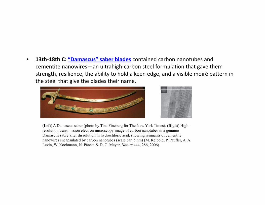
• 13th‐18th C: “Damascus” saber blades contained carbon nanotubes and cementite nanowires—an ultrahigh‐carbon steel formulation that gave them strength, resilience, the ability to hold a keen edge, and a visible moiré pattern in the steel that give the blades their name.
(Left) A Damascus saber (photo by Tina Fineberg for The New York Times). (Right) High-resolution transmission electron microscopy image of carbon nanotubes in a genuine Damascus sabre after dissolution in hydrochloric acid, showing remnants of cementitenanowires encapsulated by carbon nanotubes (scale bar, 5 nm) (M. Reibold, P. Paufler, A. A.nanowires encapsulated by carbon nanotubes (scale bar, 5 nm) (M. Reibold, P. Paufler, A. A. Levin, W. Kochmann, N. Pätzke & D. C. Meyer, Nature 444, 286, 2006).
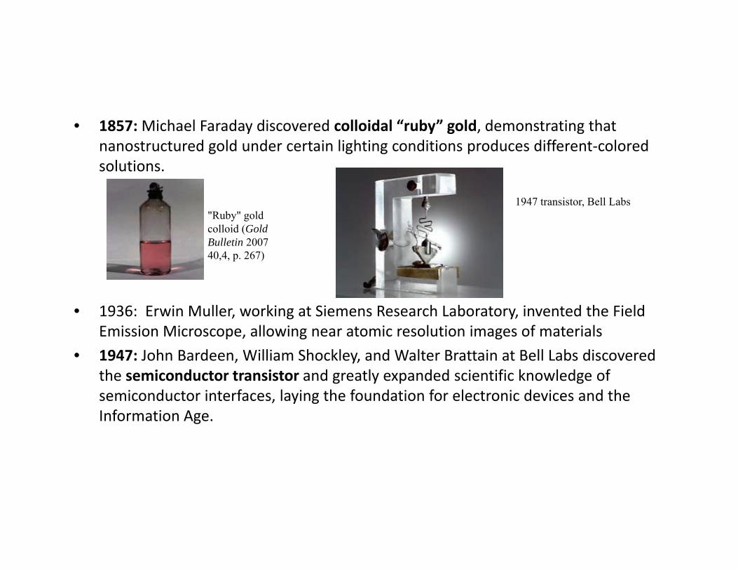
• 1857:Michael Faraday discovered colloidal “ruby” gold, demonstrating that nanostructured gold under certain lighting conditions produces different‐colored solutions.
"Ruby" gold colloid (Gold Bulletin 2007
1947 transistor, Bell Labs
• 1936: Erwin Muller, working at Siemens Research Laboratory, invented the Field
40,4, p. 267)
Emission Microscope, allowing near atomic resolution images of materials
• 1947: John Bardeen, William Shockley, and Walter Brattain at Bell Labs discovered the semiconductor transistor and greatly expanded scientific knowledge of semiconductor interfaces laying the foundation for electronic devices and thesemiconductor interfaces, laying the foundation for electronic devices and the Information Age.
• 1950: Victor La Mer and Robert Dinegar developed the theory and a process for growing monodisperse colloidal materials. Controlled ability to fabricate colloids enables myriad industrial uses such as specialized papers, paints, and thin films,
di l i t t teven dialysis treatments.
• 1951: Erwin Müller pioneered the field ion microscope, a means to image the arrangement of atoms at the surface of a sharp metal tip; he first imaged tungsten atoms.atoms.
• 1956: Arthur von Hippel at MIT introduced many concepts of—and coined the term—“molecular engineering” as applied to dielectrics, ferroelectrics, and piezoelectrics
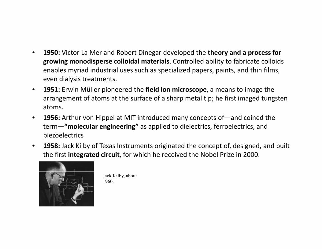
• 1958: Jack Kilby of Texas Instruments originated the concept of, designed, and built the first integrated circuit, for which he received the Nobel Prize in 2000.
Jack Kilby, about 1960.
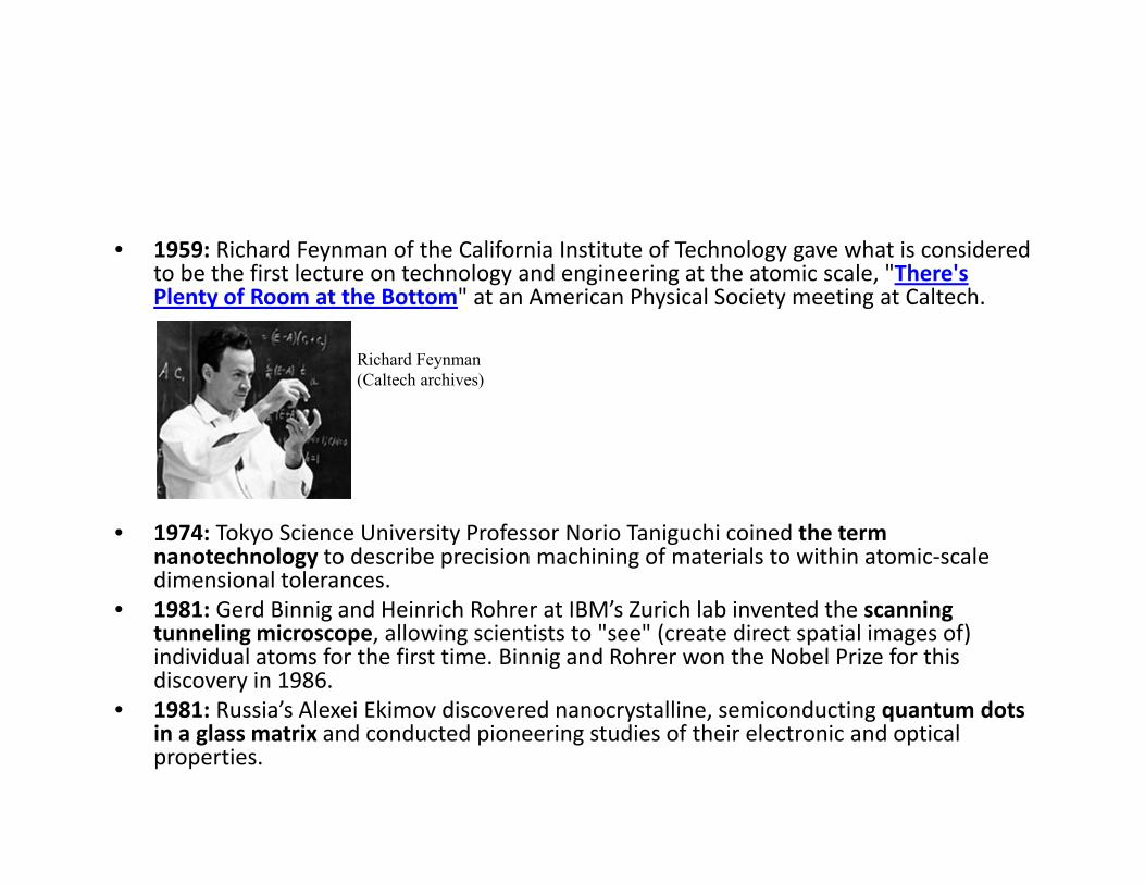
• 1959: Richard Feynman of the California Institute of Technology gave what is considered to be the first lecture on technology and engineering at the atomic scale "There'sto be the first lecture on technology and engineering at the atomic scale, There s Plenty of Room at the Bottom" at an American Physical Society meeting at Caltech.
Richard Feynman (Caltech archives)( )
• 1974: Tokyo Science University Professor Norio Taniguchi coined the term nanotechnology to describe precision machining of materials to within atomic‐scale dimensional tolerances.
• 1981: Gerd Binnig and Heinrich Rohrer at IBM’s Zurich lab invented the scanning• 1981: Gerd Binnig and Heinrich Rohrer at IBM s Zurich lab invented the scanning tunneling microscope, allowing scientists to "see" (create direct spatial images of) individual atoms for the first time. Binnig and Rohrer won the Nobel Prize for this discovery in 1986.
• 1981: Russia’s Alexei Ekimov discovered nanocrystalline, semiconducting quantum dots y g qin a glass matrix and conducted pioneering studies of their electronic and optical properties.
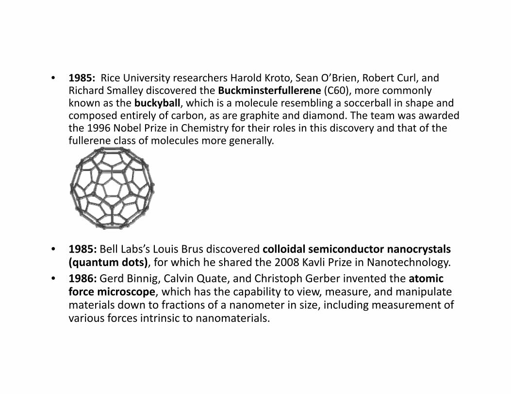
• 1985: Rice University researchers Harold Kroto, Sean O’Brien, Robert Curl, and Richard Smalley discovered the Buckminsterfullerene (C60), more commonly known as the buckyball, which is a molecule resembling a soccerball in shape and composed entirely of carbon, as are graphite and diamond. The team was awarded the 1996 Nobel Prize in Chemistry for their roles in this discovery and that of the fullerene class of molecules more generally.
• 1985: Bell Labs’s Louis Brus discovered colloidal semiconductor nanocrystals(quantum dots), for which he shared the 2008 Kavli Prize in Nanotechnology.
• 1986: Gerd Binnig, Calvin Quate, and Christoph Gerber invented the atomic force microscope, which has the capability to view, measure, and manipulate materials down to fractions of a nanometer in size, including measurement of various forces intrinsic to nanomaterials.various forces intrinsic to nanomaterials.
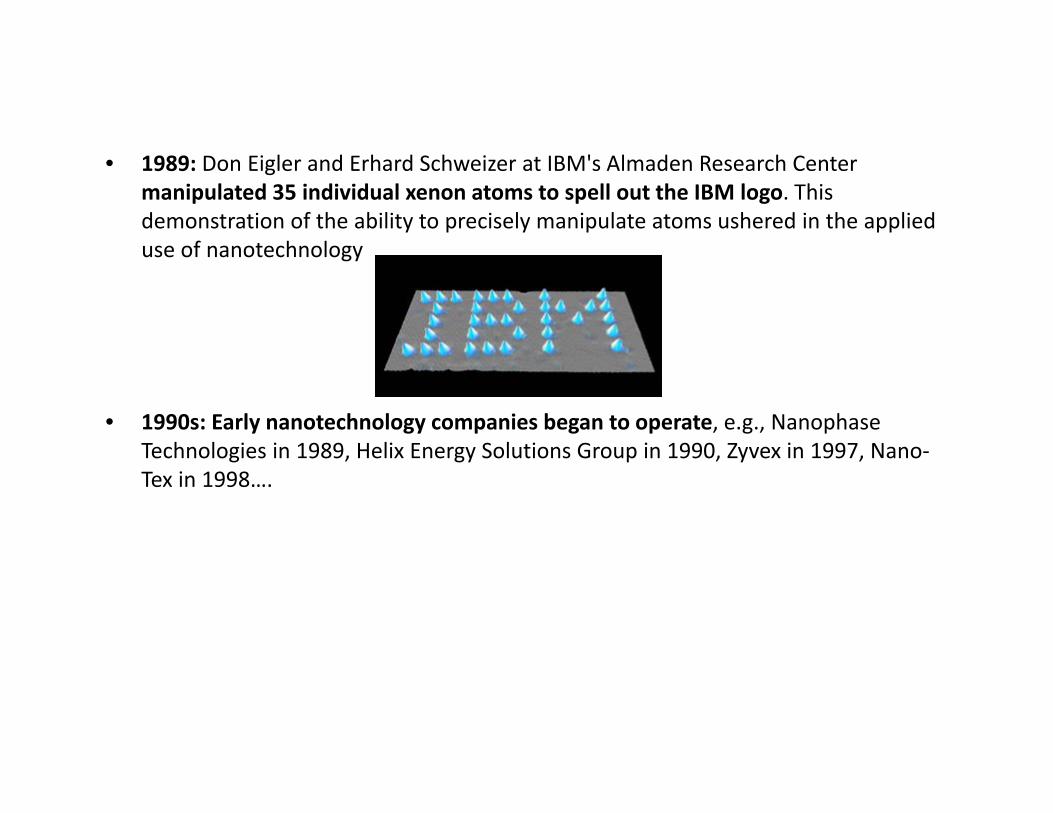
• 1989: Don Eigler and Erhard Schweizer at IBM's Almaden Research Center manipulated 35 individual xenon atoms to spell out the IBM logo. This demonstration of the ability to precisely manipulate atoms ushered in the applied use of nanotechnologyuse of nanotechnology
• 1990s: Early nanotechnology companies began to operate, e.g., Nanophase Technologies in 1989, Helix Energy Solutions Group in 1990, Zyvex in 1997, Nano‐Technologies in 1989, Helix Energy Solutions Group in 1990, Zyvex in 1997, NanoTex in 1998….
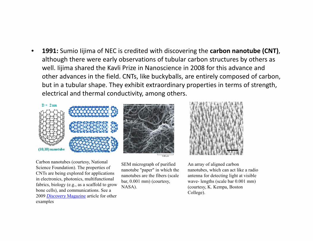
• 1991: Sumio Iijima of NEC is credited with discovering the carbon nanotube (CNT), although there were early observations of tubular carbon structures by others as well. Iijima shared the Kavli Prize in Nanoscience in 2008 for this advance and th d i th fi ld CNT lik b k b ll ti l d f bother advances in the field. CNTs, like buckyballs, are entirely composed of carbon,
but in a tubular shape. They exhibit extraordinary properties in terms of strength, electrical and thermal conductivity, among others.
Carbon nanotubes (courtesy, National S i F d i ) Th i f
SEM micrograph of purified An array of aligned carbon Science Foundation). The properties of CNTs are being explored for applications in electronics, photonics, multifunctional fabrics, biology (e.g., as a scaffold to grow bone cells), and communications. See a 2009 Discovery Magazine article for other
g p pnanotube "paper" in which the nanotubes are the fibers (scale bar, 0.001 mm) (courtesy, NASA).
y gnanotubes, which can act like a radio antenna for detecting light at visible wave- lengths (scale bar 0.001 mm) (courtesy, K. Kempa, Boston College).
2009 Discovery Magazine article for other examples
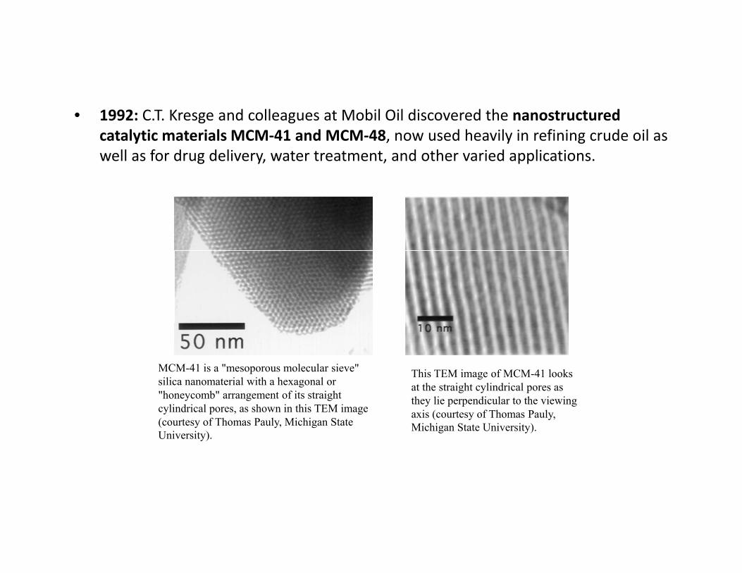
• 1992: C.T. Kresge and colleagues at Mobil Oil discovered the nanostructured catalytic materials MCM‐41 and MCM‐48, now used heavily in refining crude oil as well as for drug delivery, water treatment, and other varied applications.
MCM-41 is a "mesoporous molecular sieve" silica nanomaterial with a hexagonal or "honeycomb" arrangement of its straight
This TEM image of MCM-41 looks at the straight cylindrical pores as
honeycomb arrangement of its straight cylindrical pores, as shown in this TEM image (courtesy of Thomas Pauly, Michigan State University).
they lie perpendicular to the viewing axis (courtesy of Thomas Pauly, Michigan State University).
• 1993: Moungi Bawendi of MIT invented a method for controlled synthesis of nanocrystals (quantum dots), paving the way for applications ranging from computing to biology to high‐efficiency photovoltaics and lighting. Within the next several years, work by other researchers such as Louis Brus and Chris Murray also contributed methods for synthesizing quantum dots.
• 1998: The Interagency Working Group on Nanotechnology (IWGN) was formed under the National Science and Technology Council to investigate the state of the art in nanoscale science and technology and to forecast possible future developments. The IWGN’s study and report, Nanotechnology Research Directions: Vision for the Next Decade (1999) defined the vision for and led directly to formation of the U.S. National Nanotechnology Initiative in 2000.U.S. National Nanotechnology Initiative in 2000.
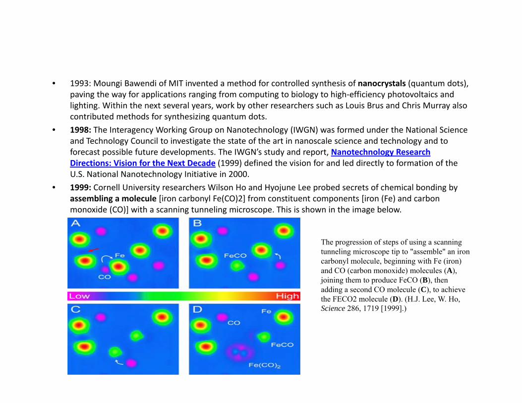
• 1999: Cornell University researchers Wilson Ho and Hyojune Lee probed secrets of chemical bonding by assembling a molecule [iron carbonyl Fe(CO)2] from constituent components [iron (Fe) and carbon monoxide (CO)] with a scanning tunneling microscope. This is shown in the image below.
The progression of steps of using a scanning tunneling microscope tip to "assemble" an iron carbonyl molecule, beginning with Fe (iron) and CO (carbon monoxide) molecules (A), j i i th t d F CO (B) thjoining them to produce FeCO (B), then adding a second CO molecule (C), to achieve the FECO2 molecule (D). (H.J. Lee, W. Ho, Science 286, 1719 [1999].)
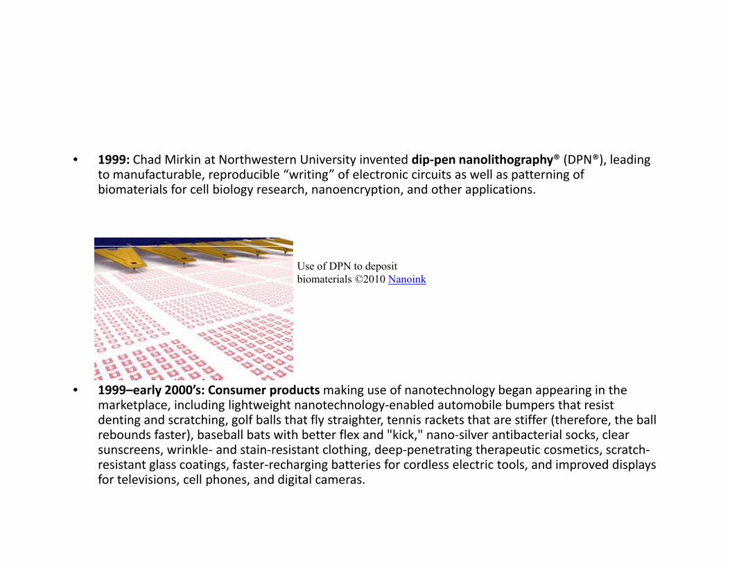
• 1999: Chad Mirkin at Northwestern University invented dip‐pen nanolithography® (DPN®), leading to manufacturable reproducible “writing” of electronic circuits as well as patterning ofto manufacturable, reproducible writing of electronic circuits as well as patterning of biomaterials for cell biology research, nanoencryption, and other applications.
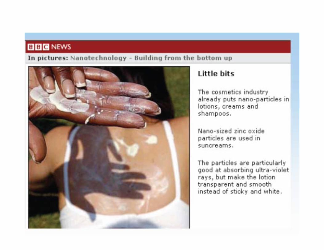
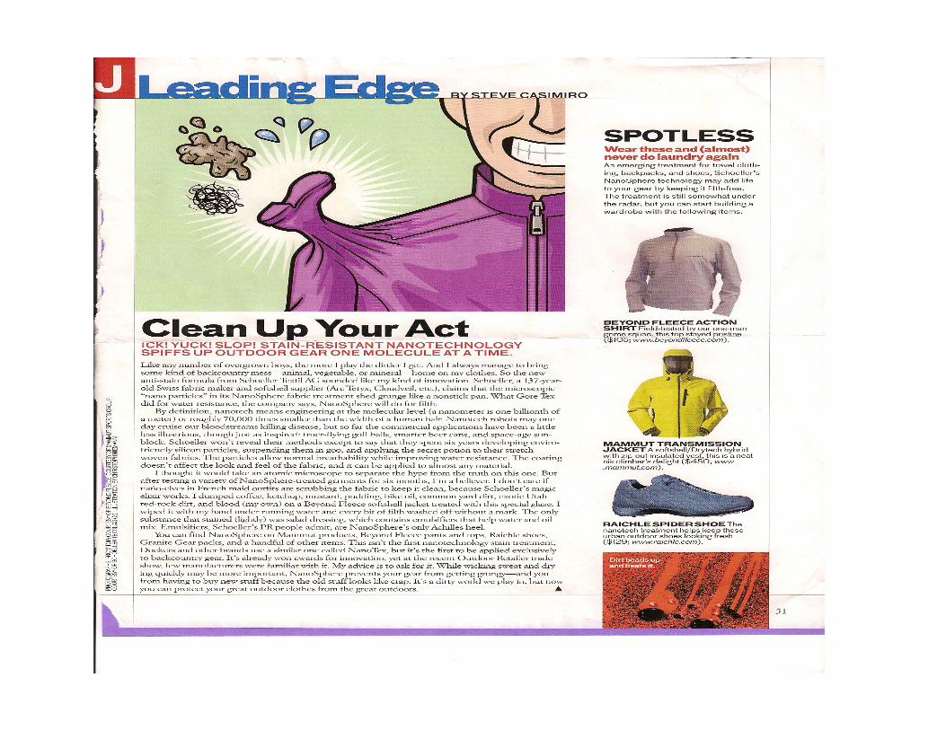
• 1999 early 2000’s: Consumer productsmaking use of nanotechnology began appearing in the• 1999–early 2000’s: Consumer productsmaking use of nanotechnology began appearing in the marketplace, including lightweight nanotechnology‐enabled automobile bumpers that resist denting and scratching, golf balls that fly straighter, tennis rackets that are stiffer (therefore, the ball rebounds faster), baseball bats with better flex and "kick," nano‐silver antibacterial socks, clear sunscreens, wrinkle‐ and stain‐resistant clothing, deep‐penetrating therapeutic cosmetics, scratch‐resistant glass coatings, faster‐recharging batteries for cordless electric tools, and improved displays for televisions, cell phones, and digital cameras.
• 2000: President Clinton launched the National Nanotechnology Initiative (NNI) to coordinate• 2000: President Clinton launched the National Nanotechnology Initiative (NNI) to coordinate Federal R&D efforts and promote U.S. competitiveness in nanotechnology. Congress funded the NNI for the first time in FY2001. The NSET Subcommittee of the NSTC was designated as the interagency group responsible for coordinating the NNI.
• 2003: Congress enacted the 21st Century Nanotechnology Research and Development Act (P.L. 108‐153). The act provided a statutory foundation for the NNI, established programs, assigned agency responsibilities, authorized funding levels, and promoted research to address key issues.
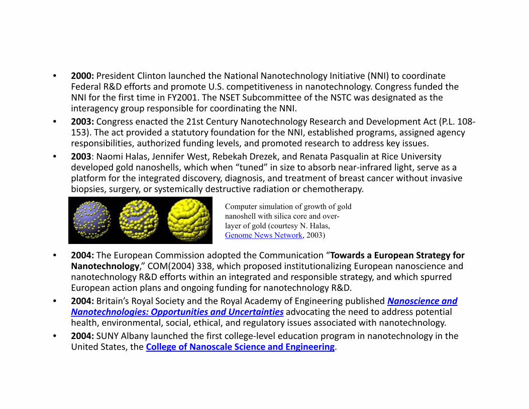
• 2003: Naomi Halas, Jennifer West, Rebekah Drezek, and Renata Pasqualin at Rice University developed gold nanoshells, which when “tuned” in size to absorb near‐infrared light, serve as a platform for the integrated discovery diagnosis and treatment of breast cancer without invasiveplatform for the integrated discovery, diagnosis, and treatment of breast cancer without invasive biopsies, surgery, or systemically destructive radiation or chemotherapy.
Computer simulation of growth of gold nanoshell with silica core and over-layer of gold (courtesy N. Halas,
• 2004: The European Commission adopted the Communication “Towards a European Strategy for Nanotechnology,” COM(2004) 338, which proposed institutionalizing European nanoscience and nanotechnology R&D efforts within an integrated and responsible strategy, and which spurred
Genome News Network, 2003)
European action plans and ongoing funding for nanotechnology R&D.• 2004: Britain’s Royal Society and the Royal Academy of Engineering published Nanoscience and
Nanotechnologies: Opportunities and Uncertainties advocating the need to address potential health, environmental, social, ethical, and regulatory issues associated with nanotechnology.2004 SUNY Alb l h d th fi t ll l l d ti i t h l i th• 2004: SUNY Albany launched the first college‐level education program in nanotechnology in the United States, the College of Nanoscale Science and Engineering.
• 2005: Erik Winfree and Paul Rothemund from the California Institute of Technology developed theories for DNA‐based computation and “algorithmic self‐assembly” in which computations are embedded in the process of nanocrystal growth.
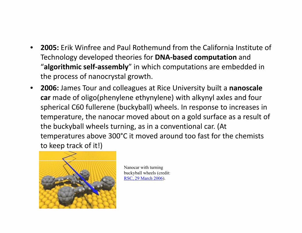
• 2006: James Tour and colleagues at Rice University built a nanoscale carmade of oligo(phenylene ethynylene) with alkynyl axles and four spherical C60 fullerene (buckyball) wheels. In response to increases in temperature, the nanocar moved about on a gold surface as a result of the buckyball wheels turning, as in a conventional car. (At temperatures above 300°C it moved around too fast for the chemists to keep track of it!)
Nanocar with turning buckyball wheels (credit: RSC, 29 March 2006).
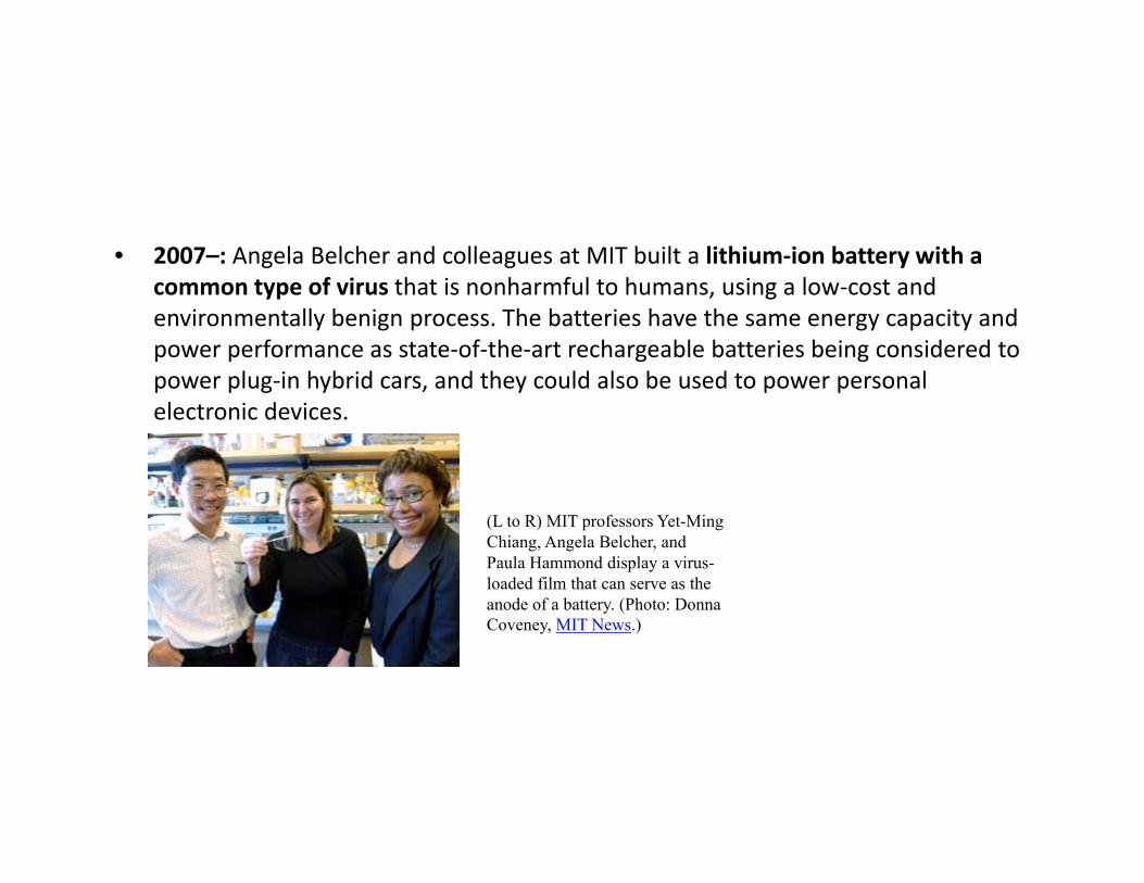
• 2007–: Angela Belcher and colleagues at MIT built a lithium‐ion battery with a common type of virus that is nonharmful to humans, using a low‐cost and environmentally benign process. The batteries have the same energy capacity and power performance as state‐of‐the‐art rechargeable batteries being considered to power plug‐in hybrid cars, and they could also be used to power personalpower plug in hybrid cars, and they could also be used to power personal electronic devices.
(L to R) MIT professors Yet-Ming Chiang, Angela Belcher, and Paula Hammond display a virus-loaded film that can serve as the anode of a battery. (Photo: Donnaanode of a battery. (Photo: Donna Coveney, MIT News.)
• 2008: The first official NNI Strategy for Nanotechnology‐Related2008: The first official NNI Strategy for Nanotechnology Related Environmental, Health, and Safety (EHS) Research was published, based on a two‐year process of NNI‐sponsored investigations and public dialogs. This strategy document was updated in 2011, following a series of workshops and public reviewfollowing a series of workshops and public review.
• 2009–2010: Nadrian Seeman and colleagues at New York University created several DNA‐like robotic nanoscale assembly devices. One is a process for creating 3D DNA structures using syntheticis a process for creating 3D DNA structures using synthetic sequences of DNA crystals that can be programmed to self‐assemble using “sticky ends” and placement in a set order and orientation. Nanoelectronics could benefit: the flexibility and density that 3D nanoscale components allow could enabledensity that 3D nanoscale components allow could enable assembly of parts that are smaller, more complex, and more closely spaced. Another Seeman creation (with colleagues at China’s Nanjing University) is a “DNA assembly line.” For this work, Seemanshared the Kavli Prize in Nanoscience in 2010.
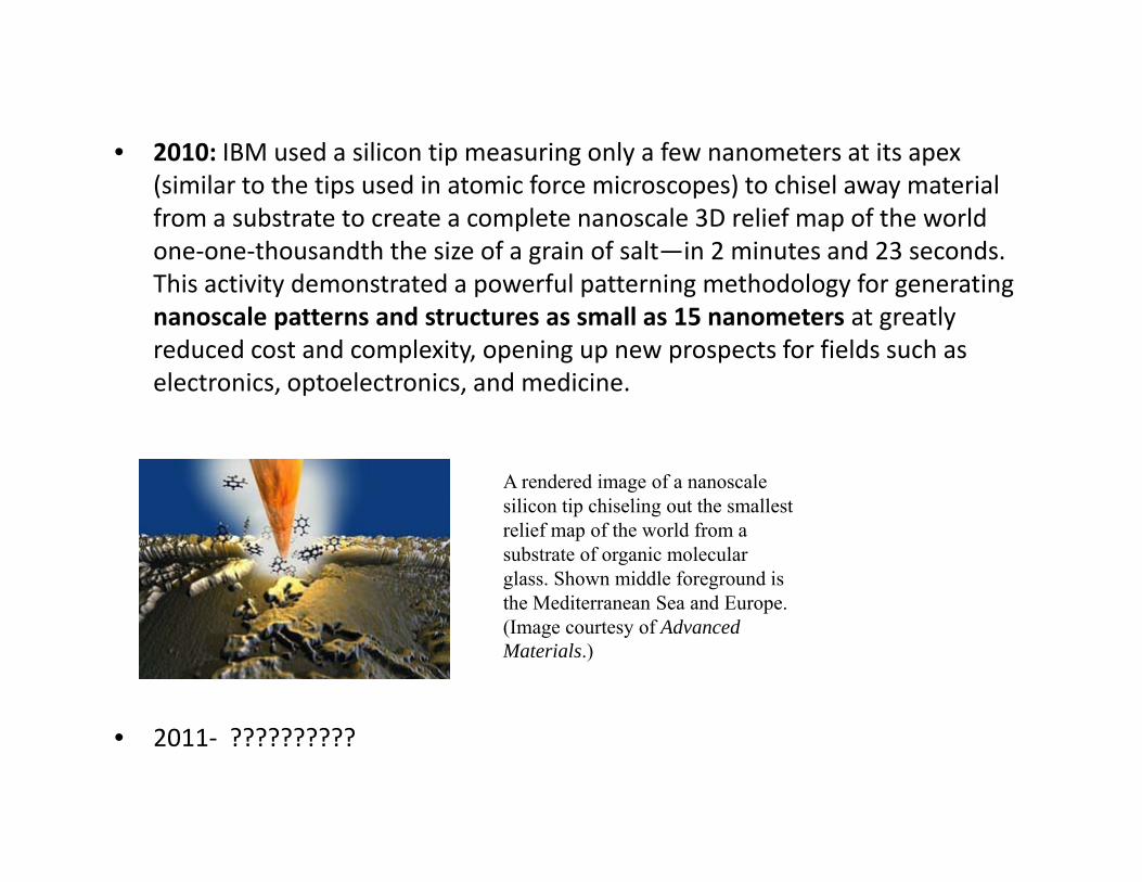
• 2010: IBM used a silicon tip measuring only a few nanometers at its apex p g y p(similar to the tips used in atomic force microscopes) to chisel away material from a substrate to create a complete nanoscale 3D relief map of the world one‐one‐thousandth the size of a grain of salt—in 2 minutes and 23 seconds. h d d f l h d l fThis activity demonstrated a powerful patterning methodology for generating nanoscale patterns and structures as small as 15 nanometers at greatly reduced cost and complexity, opening up new prospects for fields such as electronics optoelectronics and medicineelectronics, optoelectronics, and medicine.
A rendered image of a nanoscale silicon tip chiseling out the smallest relief map of the world from a substrate of organic molecular glass. Shown middle foreground is the Mediterranean Sea and Europe.the Mediterranean Sea and Europe. (Image courtesy of Advanced Materials.)
• 2011‐ ??????????
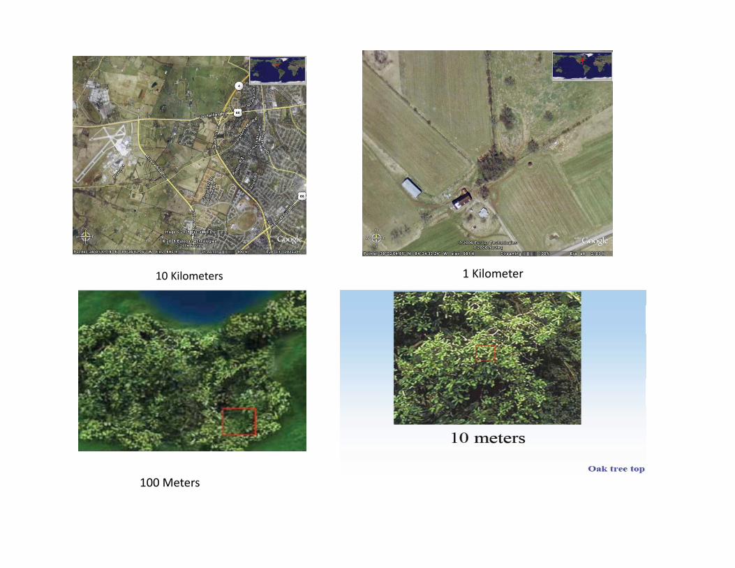
10,000 Kilometers 1000 Kilometers
100 Kilometers 10 Kilometers
10 Kilometers 1 Kilometer
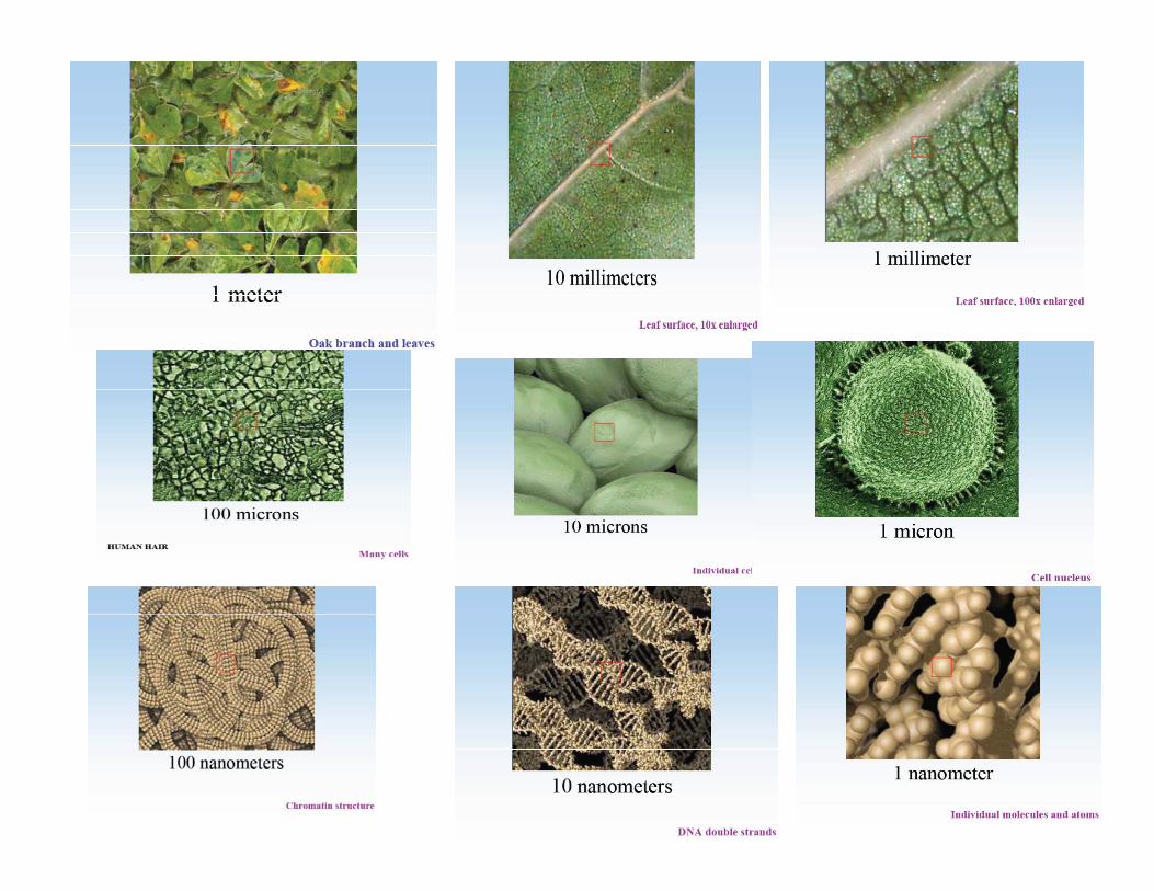
100 Meters
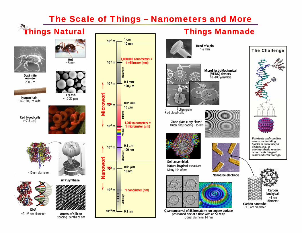
Things NaturalThings Natural Things ManmadeThings Manmade1 cm10 mm
10-2 m
The Scale of Things The Scale of Things –– Nanometers and MoreNanometers and More
Head of a pin1-2 mm
Ant~ 5 mm
The Challenge
1 millimeter (mm)
10 mm
10-3 m
wave
1,000,000 nanometers =
MicroElectroMechanical
Fly ash~ 10-20 mHuman hair
~ 60-120 m wide
Dust mite
200 m
OP
O
Owor
l0 01
0.1 mm100 m10-4 m
Micr
o (MEMS) devices10 -100 m wide
Red blood cells(~7-8 m)
60 120 m wideO O OO
O OO O OO OO
O
S
O
S
O
S
O
S
O
S
O
S
O
S
O
SMic
row d
1 micrometer (m)
0.01 mm10 m10-5 m
10-6 mbl
e1,000 nanometers =
Infra
red
Zone plate x-ray “lens”Outer ring spacing ~35 nm
Red blood cellsPollen grain
Fabricate and combine nanoscale building blocks to make useful devices, e.g., a photosynthetic reaction center with integral semiconductor storage.
0.1 m100 nm10-7 m
Visib
orl
Ultra
violet
S lf bl d
ATP synthase
~10 nm diameterNanotube electrode
1 nanometer (nm)
0.01 m10 nm
10-8 m
10-9 m
Nan
owo
d
U
Carbon
Self-assembled,Nature-inspired structureMany 10s of nm
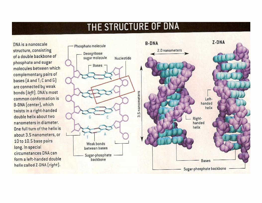
DNA~2-1/2 nm diameter Atoms of silicon
spacing ~tenths of nm
Quantum corral of 48 iron atoms on copper surfacepositioned one at a time with an STM tip
Corral diameter 14 nm
Carbon nanotube~1.3 nm diameter
0.1 nm
1 nanometer (nm)10 m
10-10 m
Soft
x-ra
y
Carbon buckyball
~1 nm diameter
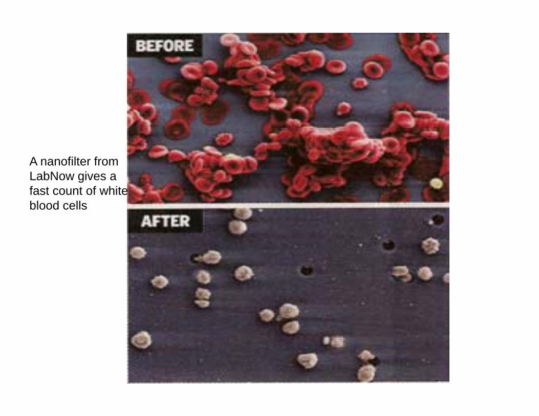
A nanofilter from LabNow gives a gfast count of whiteblood cells
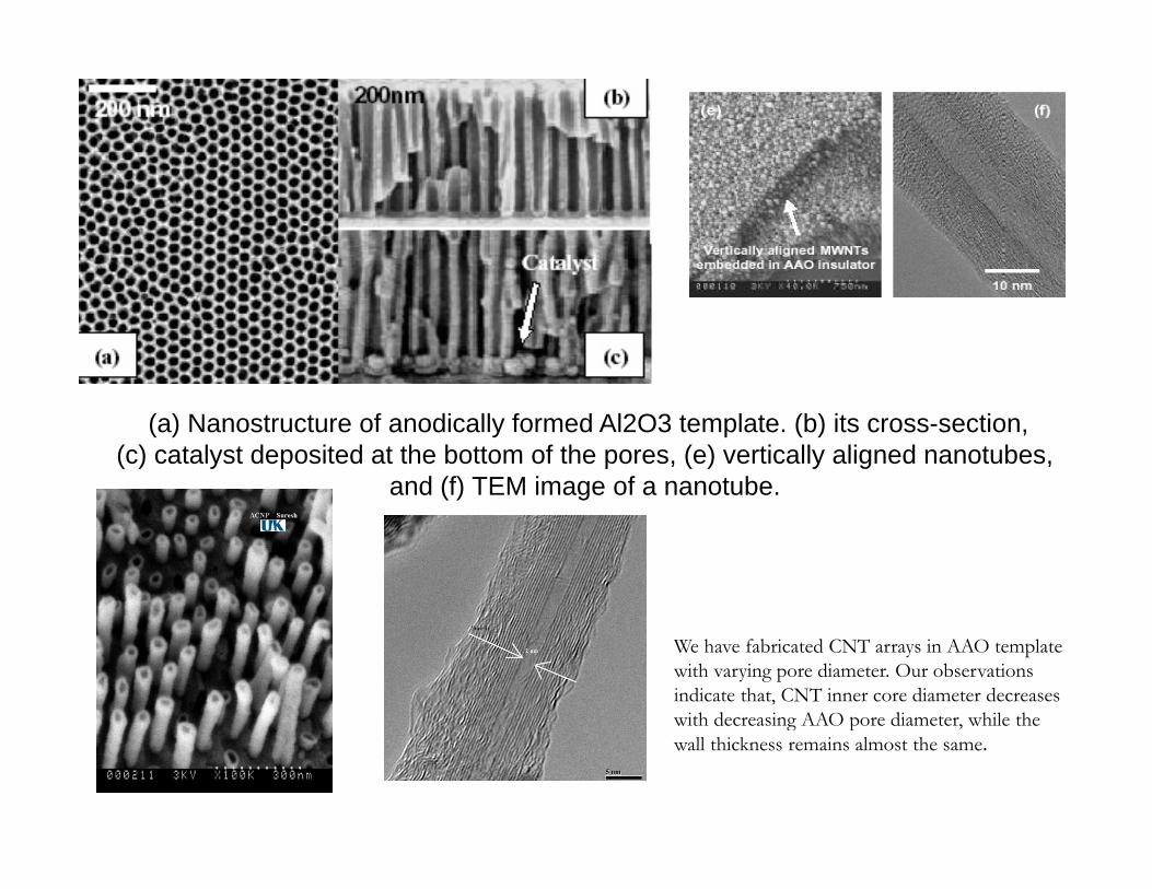
(a) Nanostructure of anodically formed Al2O3 template. (b) its cross-section, (c) catalyst deposited at the bottom of the pores, (e) vertically aligned nanotubes,
and (f) TEM image of a nanotube.
We have fabricated CNT arrays in AAO template with varying pore diameter. Our observations indicate that, CNT inner core diameter decreases with decreasing AAO pore diameter, while thewith decreasing AAO pore diameter, while the wall thickness remains almost the same.
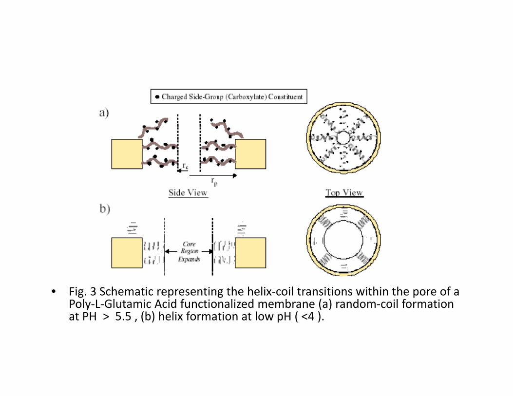
• Fig. 3 Schematic representing the helix‐coil transitions within the pore of a Poly‐L‐Glutamic Acid functionalized membrane (a) random‐coil formation at PH > 5.5 , (b) helix formation at low pH ( <4 ).
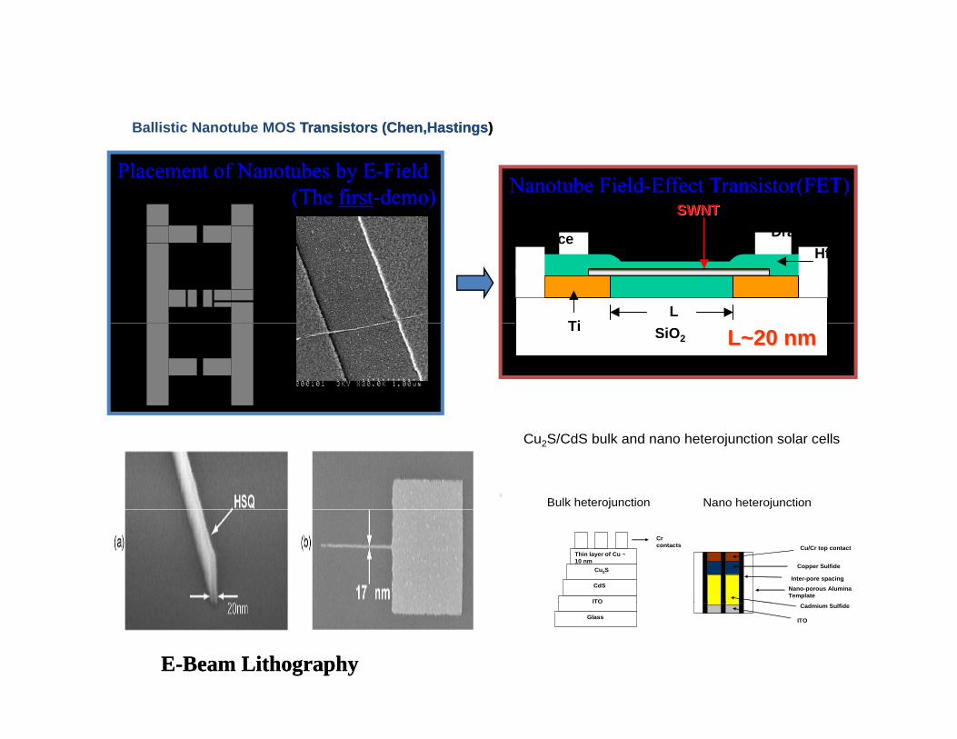
Ballistic Nanotube MOS Transistors (Chen,HastingsTransistors (Chen,Hastings))
D
SWNTSWNTAl-GateDrain
Placement of Nanotubes by EPlacement of Nanotubes by E--FieldField(The (The firstfirst--demo)demo) Nanotube FieldNanotube Field--Effect Transistor(FET)Effect Transistor(FET)
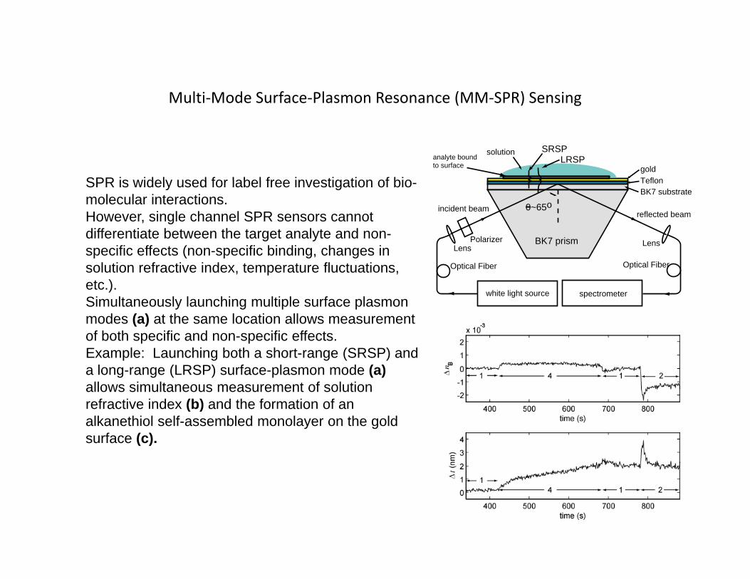
SPR is widely used for label free investigation of bio
BK7 prism
BK7 substrateTeflon
incident beamreflected beam
0~65o
Lens LensPolarizer
SPR is widely used for label free investigation of bio-molecular interactions. However, single channel SPR sensors cannot differentiate between the target analyte and non-specific effects (non-specific binding changes in
white light source spectrometer
Optical Fiber Optical Fiberspecific effects (non specific binding, changes in solution refractive index, temperature fluctuations, etc.).Simultaneously launching multiple surface plasmon modes (a) at the same location allows measurement ( )of both specific and non-specific effects.Example: Launching both a short-range (SRSP) and a long-range (LRSP) surface-plasmon mode (a)allows simultaneous measurement of solution
f ti i d (b) d th f ti frefractive index (b) and the formation of an alkanethiol self-assembled monolayer on the gold surface (c).
Application as Functional Components of Novel DevicesDevices
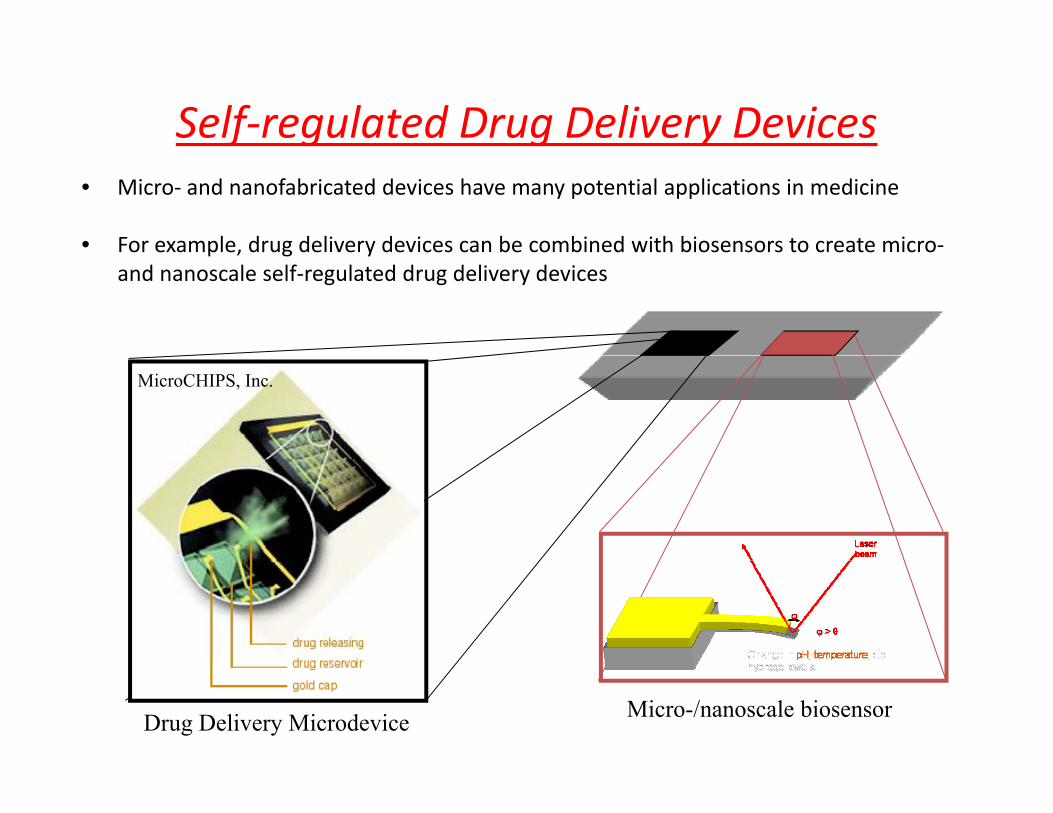
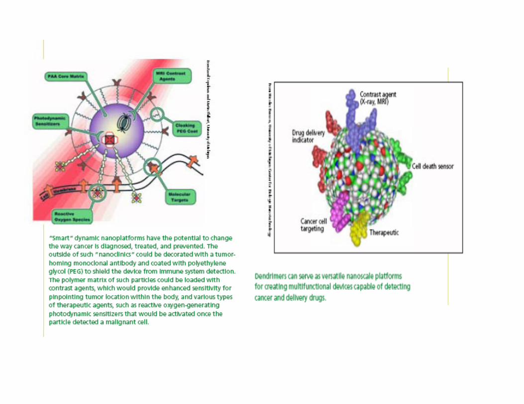
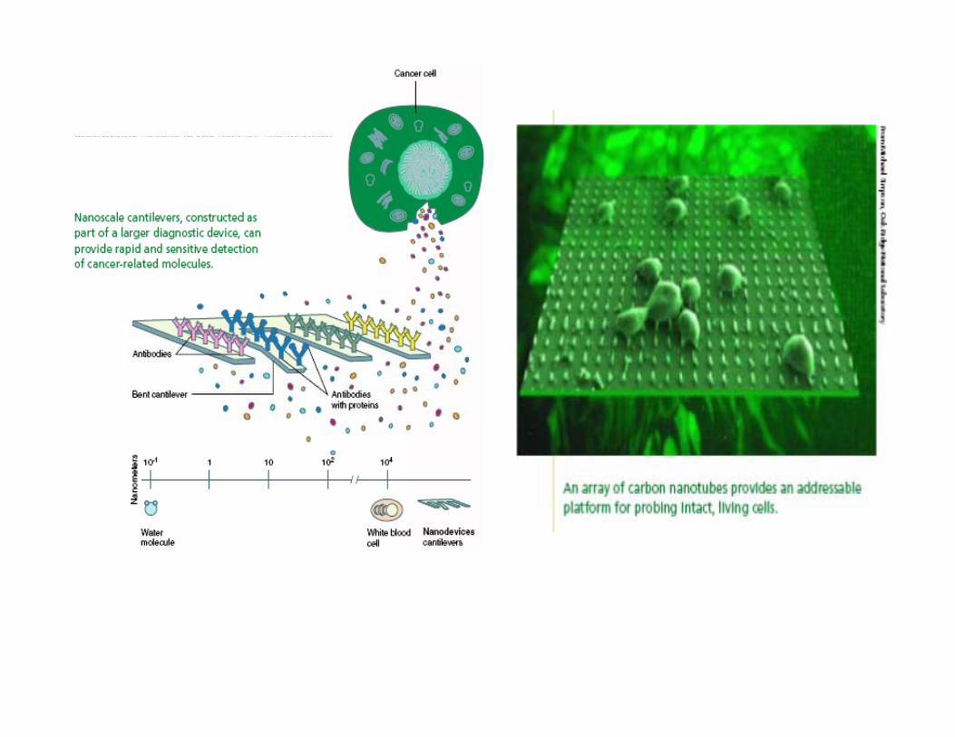
• Nanomedicine
Di i– Diagnosis• Imaging• Sensors• DNA Sequencing
– Arrays, Nanopore Sequencing
– Therapeutics• Surgery• Drug DevelopmentDrug Development


![Introduction - CS Multimedia Lab · PDF fileThe$Lycurgus$Cup,$an$earlyexample$of$ dichroic$glass$[4]$ Tony Wang Professor Scarlatos HON 301 October 19th, 2014 The Application of DNA](https://static.documents.pub/doc/80x56/5aaf48497f8b9adb688d7353/introduction-cs-multimedia-lab-lycurguscupanearlyexampleof-dichroicglass4.jpg)


