Advances in Technologies, Architectures, and Applications
of Highly-Integrated Low-Power Radars
Bruno Neri & Sergio Saponara University of Pisa
INTRODUCTION
The basis of radar (RAdio Detection And Ranginl) theory and technique dates back to the beginning of the 20 century, although the development of such technology was pushed by military applications during WW II with high-power (up to several kW and more), large size, long-distance radars. The radar technique has since been adopted for civil applications: e.g., Long Range Radar (LRR) for obstacle detection on-board airplanes and ships, traffic control in airports, long distance measurements, and remote sensing.
Recent advances in silicon technologies and electronic design methods, make possible the realization of highly-integrated radars with low cost, compact size, and low power consumption. This enables the widespread adoption of radar for new civil and defense applications such as [ 1 -20] : automotive short-range radars (SRR) for car parking, side-crash warning, collision warning, blind-spot detection and "stop and go " control in urban scenarios; automotive LRR for adaptive cruise control (ACC); SRR for contactless heart and pulmonary monitoring in e-health applications; SRR for vital signs detection in case of natural disasters or war scenarios; distance measurements in industrial automation; mm-wave body scanner for security; e.g., in airports and banks; ground penetrating applications; intra-wall and through-wall detections.
According to forecast market analysis [ 1 , 2] , in 2014, 7% of all vehicles sold world-wide, particularly in Europe, Japan, and the US, will be equipped with radar systems with a market value of billions of US dollars.
Such radar systems have some common characteristics: radar modulation schemes are pulsed Ultra WideBand (UWB)
Author's ClIITeIlt Address: B. Neri and S. Saponara, University of Pis&, Department of Information Engineering, via G. Caruso 1 6, 56122, Pis&, Itsly.
Fig. 1. EIRP Power Spectral Density in dBmIMHz in ETSI and FCC
.;
111 83
for SRR applications within 1 0 m, and Frequency Modulated Continuous Wave (FMCW) for mid- and long-range applications as high as several hundreds of meters. SRRs operate below 10 GHz or around 24 GHz, while LRRs operate at higher frequencies, such as 77-8 1 GHz where there are less strict limitations in terms of output power spectral density (PSD) [ 1 , 3] .
Figure 1 reports, for ETSI (European Telecommunications Standards Institute) and FCC (Federal Communications Commission) standards, the EIRP (Equivalent Isotropically Radiated Power) spectral density expressed in dBmlMHz [ I , 2]. Note that at 77 GHz there is a path loss of roughly 1 50 dB at 100 m distance, and hence, high gain antennas and high sensitivity receivers are required for LRR applications.
The output transmitted power of integrated radars typically amounts to a few dBm. For power levels in the order of Watts, or higher, off-chip power amplifiers (PA) are needed.
Figure 2 reports the main characteristics of SRR and LRR automotive systems: modulation used (Mod.), center frequency (Freq.) and bandwidth (BW), antenna aperture
25
S RR
Freq. BW Range Resol. Peak PSD Mod. 0 dBm! GHz GHz power m m dBm
SRR pulsed 24 7 700 1 0 <0. 1 -4 1 .3
SRR pulsed 79 4 700 1 0 <0 . 1 - 9
LRR FMCW 77 1 <200 1 00 1 5 5
Fig. 2 . Automotive Radar Specifications
angle (0), ranging distance (Range), and resolution (Resol.), peak power and PSD. The values of peak power and PSD refer to the limits adopted in Germany [ 1 ] .
The success of such applications in large volume markets requires the single-chip or at least the single package integration of mm-wave radar transceiver and base-band Digital Signal Processor (DSP).
Herein, the state-of-the-art of design realization and utilization of highly integrated low power radar will be described. Particularly, in the section entitled Technologies for Highly-Integrated and Low-Power Radars, the possible radar integration levels and the evolution in semiconductor technologies toward single-chip radar implementation will be reviewed. In the Radar Equations and Architecture Sizing section, the main equations to be used for specifying the radar parameters, starting from the application requirements, are shown. The Architectures and Performance of Pulsed and CW Highly-Integrated Radars section discusses the architecture and the main design criteria for FMCW and pulsed radars, the challenging issues toward the integration of the radar on a single-chip and the achievable performance in low-cost CMOS technologies. Two case studies will be analyzed: a 77 GHz automotive LRR design, requiring a dedicated DSP unit, and a pulsed SRR for e-health applications, working in the 3-10 GHz UWB spectrum. Moreover, implementation results (circuit complexity and radar performance) of state-of-the-art highly-integrated radars are presented [4-20]. Finally, recent research results achieved by the authors when designing key components of the highly-integrated radar are discussed [2 1 -26] : a low-power threshold-configuring SAR (Successive Approximation Register) AnaloglDigital (AID) Converter [25, 26], a pipeline cascade Fast Fourier Transform (FFT) hardware co-processor [2 1 , 22], mm-wave Low Noise
26
Amplifier (LNA) and integrated mm-wave double-slot antenna [23] . Conclusions are drawn in the final section.
TECHNOLOGIES FOR IDGHLY-INTEGRATED AND LOW-POWER RADARS
Radar Integration Levels From the implementation technology point of
view, different levels of integration are possible for miniaturized and low-power radars: System-on-a-single-Chip (SoC) where the radar is completely contained in a single chip, System-in-a-Package (SiP) where the radar is realized using multiple chips but embedded in a single package, or single-board radar where the system is realized using multiple integrated circuits mounted on a single board.
With reference to a pulsed modulation scheme, Figure 3 shows the main blocks of a radar: an antenna array used in timed-division for the transmitter (TX) and the receiver (RX); the transceiver with a homo dyne RX chain using the same reference oscillator of the transmitter to detect the Doppler frequency shift; AID and DI A converters; a base-band DSP unit for 1) Time-Of-Flight (TOF) and Doppler shift detection and processing in the RX path, 2) waveform generation for scanning radar in the TX path, and 3) user interfacing.
Today, the main challenge addressed by radar-on-chip designs is integrating on a single chip of a few mm2 the whole TX and RX chains operating in the mm-wave domain. At the state-of-the-art, the AID and DI A converters and the based-band DSP unit are typically implemented on a separate silicon die, integrated with the mm-wave transceiver chip in a single package or mounted on a single Printed-Circuit-Board (PCB).
Fig. 3 . Architecture of a Pulsed Radar with Homodyne-Type Receiver
The trend for the future, thanks to the evolution in silicon technologies, is further increasing the miniaturization level integrating in a single-chip the radar transceiver plus the AID and Df A converters and part of the DSP chain, such as an FFT processor.
As far as the antenna is concerned, it is typically realized off-chip. Indeed, LRR applications require antennas with high gain (e.g., from 20 dB up to 25 dB with a patch, hom, or dish antenna as in [4, 7, 1 1 ]) and high directivity which can not be realized on-chip. For radars operating at frequencies below 1 0 GHz, the wavelength amounts to several cm, and hence, it is not convenient to integrate the antenna due to the high silicon area occupied.
Single-chip integrated antennas on Silicon-on-Insulator (Sol) technology have been recently proposed in literature [23 , 27] but only for short-range and high-frequency applications: a double-slot antenna with CPW (CoPlanar Waveguide) feed, tunable to operate in the unlicensed 60 GHz band or in the 76 GHz range, has been proposed by these authors with a gain of 4.4 dB and an area occupation of 1 mm2 [23) . Further research is ongoing to increase the antenna gain and reduce the occupation area so that silicon fully-integrated SRRs operating in the 77-8 1 GHz spectrum can be a reality in the near future.
It should be noted that FMCW radars use separate TX and RX antennas [4] while pulsed radars use the same antenna in time-division for TX and RX [5] . Moreover, by using an antenna array, whose elements are driven with proper phase delays by a digital waveform generator as in Figure 3, a radar scanning effect can be obtained [4-6].
Unlike beamforming, which presumes a high correlation between signals either transmitted or received by an array, the Multiple-Input Multiple-Output (MIMO) concept exploits the independence between signals at the array elements to improve radar detection performance. In conventional single-antenna, radar target scattering is regarded as a parameter that degrades radar performance while MIMO radar takes the opposite view, capitalizing target scattering to improve the radar's performance [28-3 1 ] .
IEEE A&E SYSTEMS MAGAZINE, JANUARY 2012
Semiconductor Technologies for mm-wave Radar Transceivers ·and Base-Band DSP
The main semiconductor devices that can be used for radar design are BIT (Bipolar Junction Transistors) and MOS-FET (Metal Oxide Semiconductor Field Effect Transistors). For BIT and MOS n- and p- complementary transistors exist where the majority charge carriers are electrons and holes, respectively. Both devices can implement digital (on/off function mode) and analog circuits. In radar design BJTs are more suited for high-frequency analog circuitry ensuring higher gain, lower Noise Figure (NF) and higher cut-off frequency. MOS are more suited for the base-band DSP due to lower power consumption, easier device scaling, and hence, higher integration levels, and lower cost. BiCMOS (Bipolar Complementary MOS) and SOl CMOS technologies allow us to improve the performance of standard CMOS, although at higher cost. The BiCMOS allows the co-integration of BJT for high-frequency applications and MOS devices for digital circuits. In SOl technology the high resistivity of the substrate on which n- and p-MOSFET are created allows dielectric isolation of the circuit elements. This way, junction capacitances are reduced significantly, increasing the maximum operating frequencies. Moreover, noise coupling between digital and analog parts integrated in the same chip is reduced and the performances of antennas designed in SOl CMOS are improved due to a reduced amount of energy stored in the supporting substrate.
Thanks to the silicon technology scaling predicted by Moore, (the integration density doubles roughly every two years) the integration of complex and real-time DSP functions in a single-chip is today possible with low power consumption, low cost for high volume markets (down to few dollars per chip) and high miniaturization levels. MOS devices are available with channel length below 1 00 nm (32 nm in production) and billions of transistors that can be integrated in a single chip. Depending on the desired trade-off between flexibility and performance an Application Specific Integrated Circuit (ASIC), a Field Programmable Gate Array (FPGA) or a software-programmable processor can be designed.
27
Table 1 . Semiconductor Technologies for Radar Design
FT GainINF Ratio
BJT High High
CMOS Medium Medium
BiCMOS High High
HEMT Very IDgh High
'In [2 1] , we proposed an FFT macrocell based on a pipeline cascade architecture with mixed radix-2 and radix-4 butterflies fulfilling the DSP requirements of a Doppler radar (up to 8 192-point FFT with 1 0 MS/s throughput). This FFT processor occupies an area below 0. 1 mm2 in 65 nm CMOS technology with a power consumption below 1 mW. The same macrocell, described with VHDL language, has been synthesized on a low-cost reconfigurable device occupying 30% of a Spartan- l000 Xilinx FPGA with a power consumption of 200 mW. Spartan FPGAs are available with ABC Q- I00 automotive-grade qualification and with costs of a few dollars for large volume markets. Similar results can be obtained with FPGA devices from other providers such as ALTERA (whose configuration is stored in volatile Static Random Access Memory, SRAM, as for Xilinx) or Actel (Flash-based non-volatile devices). Hence, FPGAs are 'suitable to implement the DSP chain for the emerging automotive radar market [14, 15 , 32-35]. - Differently from digital circuits dominated by MOS
transistors, the technology selection for mm.-wave radar transceivers is not closed. This is mainly due to the challenging requirements of very low NF of few dB and high gain (tens of dB) for the LNA, high receiver sensitivity, high operating frequencies from a few GHz to 100 GHz, and more. The best performances at such high frequencies can be achieved with compound semiconductor transistors in ill-V GaAs or loP technologies due to higher mobility of electrons vs. silicon [36-39] . For example, monolithic radar transceivers using MESFET (MEtal-Semiconductor FET) or HBT (Hetero-junction Bipolar Transistor) in GaAs technology have been designed since the 1980s, see [36]. Since 2005 [37] ill-V High Electron Mobility Transistors (HEMT) with FT (the frequency at which the short-circuit current gain is 1 ) of 700 GHz ate available. Today we are in the THz domain. However due to niche market applications and higher device size, the cost of ICs with ill-V technologies is much higher than that of silicon technologies. While such cost is affordable in military or space applications, for low-cost, low-power civil radar applications, silicon technologies must be used. At the state-of-the-art the SiGe BiCMOS technology, with 1 30 nm transistors channel
28
Cost Power Suited For Consumption
Medium HIgh Analog, RF
Low Low Digital
Medium Medium Analog, RF, mixed-signal
High Medium mm-wave
length and an FT of230 GHz, offers a good trade-off between cost and performance for single-chip mm.-wave radar transceivers. Several transceivers at 24, 77, 90, 120 GHz have been proposed in literature using SiGe BiCMOS technology [6, 8- 13] . Table 1 reports a qualitative comparison of the semiconductor technologies available for highly-integrated radar design.
The next step in transceiver radar design is to use CMOS technology for the mm-wave circuits. As an effect of device scaling a FT higher than 150 GHz can be obtained with MOS transistors in sub-loo om technology nodes; therefore radar chips from a few GHz to 77 GHz can be designed in 90 nm or 65 nm CMOS technology. Realizing the same mm-wave transceiver architecture in 65 om CMOS technology entails a lower area and, consequently, lower cost for large volume market radar systems (transceiver plus DSP) but also lower performance vs. a 130 om BiCMOS SiGe technology. For example, in literature, a 24 GHz receiver with 30 dB gain and 6.5 dB NF has been proposed in 65 om CMOS technology while in 130 om SiGe BiCMOS technology, a receiver with 47 dB gain and 3 dB NF [9] is achieved for the same application.
Figure 4 reports the performance achievable at the state-of-the-art in CMOS technologies vs. the working frequency in terms of LNA gain, receiver NF, maximum deliverable power in transmission by the P A.
Figure 4 shows that the state-of-the-art mm-wave designs in CMOS technology have optimal performances (LNA gain higher than 20 dB, NF lower than 4 dB, 1 5 dBm to 30 dBm TX power), up to 10-20 GHz applications. At higher frequencies the performances decrease. Around 77 GHz acceptable but non-optimal performance are achieved today (LNA gain lower than 20 dB, NF higher than 4 dB, output power limited by 1 0 dBm).
RADAR EQUATIONS AND ARCIDTECTURE SIZING
This section discusses the fundamental equations needed to define the functional performance (e.g., ranging distance and resolution, speed detection range, Doppler resolution) and the main architectural parameters of a highly-integrated
IEEE A&E SYSTEMS MAGAZINE, JANUARY 201 2
a)
b)
c)
« 35 n. II) 30 0 :E 25 0
, 20 E !g 1 5 � 1 0 -:;, 5 0 n.
0
25 « z ...J � 20 :E 0 , to '0. 1 5 c ·cv (!)
1 0
1 0
� 8 ...J II) o 6 :E 0 � 4 '0 U: 2 z
0
[50)
+------------I�nt�·�� ��T-------�
• (45)
•
[52)
1 0 F (GHz) 1 00
• (46) ---(47)
1 000
[23T
�) • [4 [49]
• (7)
F (GHz) 1 0 1 00
[45) •
.-[52)
.[46) • [53)
F (GHz) 1 0
[41
(48) � [H
�·3l--1 00
Fig. 4: Performance Analysis for state-of-the-art CMOS mm-wave Circuits;
Fig. 4A. Output Power of Integrated PA; Fig. 4B. Gain of LNA;
Fig. 4C. NF of LNA
radar: gain and NF of the receiver from the antenna to the IF amplifier, gain and output power level of the transmitter chain including PA and antenna, FFT size and throughput of the DSP processor. The architectures ofFMCW and pulsed radars will be discussed and two design examples in low-cost CMOS technologies will be presented: a 77 GHz automotive LRR and a 3- 10 GHz UWB SRR for e-health.
Equation 1 shows how the received·power Pr depends on
radar wavelength A and hence carrier frequency fe, TX and RX antenna gains (Gt and Gr, respectively), target cross
section cr, and obviously transmitted power Pt and target distance R. Equation 2 determines the SNR at the receiver side given the Pr value obtained from Equation 1 , the NF of the receiver chain, the thermal noise contribution KT and the FFT bandwidth resolution BWFFf (which can be evaluated by
IEEE A&E SYSTEMS MAGAZINE, JANUARY 2012
dividing the sampling rate by the number of points in the FFT).
p = �GtG)}(j r (41t )3 R4
SNR = � K · T · NF · B WFFT
(1)
(2) The SNR is related to the detection probability and to the
false alarm rate of the radar system. As reported in the literature to achieve a detection probability of 99% and a negligible false alarm rate of 10-10 a SNR of at least 1 6 dB is required, further details are provided in [7] .
Combining Equations 1 and 2, and considering the specifications coming from the application and the standards, a trade-off between the different architectural parameters can be found.
Consider a 77 GHz LRR (A = 0.39 cm), the black curve in Figure 5 is obtained in terms of required PI vs. distance R assuming the following value for radar parameters: 20 dB gain TX and RX antennas; SNR of at least 1 6 dB; considering automotive target cross sections of several m2; an FFT processor similar to what we proposed in [2 1 ] (BWFFT -1 kHz, with 8 1 92 points FFT); a NF of 10 dB that can be easily realized in CMOS technology also at 77 GHz (see Figure 4). The Pr in such conditions is -88 dBm.
40
20 -I ..... , I l1li _ � �,- ...- - -
..-- ---.:..----"' _r - � ---
_ _ _ - A - '" - -4 - - -o
E � ·20 0:: ·40
·60
-80
�-- lIt - - - -- -
/' 20 " . - - - 40 ,. - - 60 80
(It/� Pt needed vs. R (10dB NF, 20 dB Gt & Gr) Il� Pt availa ble with integrated CMOS PA
I - ... - Pt needed vs. R (5db NF, 24 dB Gr & Gt) � R (m )
Fig. S. Required Pt (dBm) vs. distance R (m)
Considering a maximum PI of 10 dBm (10 m W) achievable with CMOS fully-integrated PA, a distance
1
of 50 m is covered (intersection of gray and black curves in Figure 5).
o
By considering a lower NF of 5 dB and an antenna gain of 24 dB (Pr is -93 dBm) with a PI of 10 dBm ( 1 0 mW) a target distance R of 100 m can be covered (intersection of gray and dashed curves in Figure 5).
Otherwise fixing the target distance, e.g., R = 70 m and the power level, e.g., PI = 10 dBm, and hence, Pr - -94 dBm, the curve in Figure 6 is obtained in terms of required NF and FFT performance. Different curves are obtained varying the
29
antenna gains (20 dB and 22 dB off-chip antennas are considered in Figure 6). Obviously given a fixed FFT frequency resolution, target distance and transmitted power the lower the antenna gain the lower the NF requirement (more difficult to achieve). From Figure 6 targeting a design with a NF = 5 dB, then an FFT processor with a resolution of roughly I kHz is needed (e.g., 8 1 92 point FFT with a throughput of 1 0 MS/s feasible with our pipeline cascade coprocessor in [2 1 ]) .
To cope with non-idealities of hardware components a margin should be taken by hardware designers with respect to the specifications obtained from the above analysis. If the ADC plus FFT processing chain has not degraded the required receiver SNR of at least 16 dB, then a Signal-to-Noise-and-Distortion-Ratio (SNDR) in the range 30-40 dB is needed for the AID converter. Therefore an Effective Number Of Bits (ENOB) of at least 6 bits is needed, which allows a SNDR of 36 dB. As proved in the literature [2 1 , 22, 25], to reach an ENOB performance of 6 bits, the ADC and the digital FFT processor should be designed with 7-8 nominal 110 bits.
I �OOOO • FFT-resol. (Hz) vs. NF (dB). Gr=Gt=20dB
j l • L · FFT-resol. (Hz) vs. NF (dB). Gr=Gt=22 dB • c:
I 1 1 1 000 •
• .. Ii: ........ ..
j l" 1 00 3 5 NF (dB) 7 9
Fig. 6. FFT Resolution (Hz) and NF (dB) Trade-OfT, Pt = 10 dBm, R = 70m, 77 GHz Radar Considering
Different Gr and Gt Antenna Gains
For example, the threshold-configuring SAR AID converter, proposed by us in [25] in 90 nm CMOS technology, offers 7 nominal bits and 6 ENOB with a sample rate up to 100 MS/s, beyond the 10 MS/s requirements emerging from the above analysis.
Note that the SAR ADC we proposed in [25] has been used in [26] as a basic channel of a multi-channel time-interleaved (TI) AID converter. The TI ADC is capable of sampling rates up to I GS/s required in emerging Software Defined Radio systems or multimedia processing terminals [54-58].
At the transmitter side, the use of a linear class A power amplifier minimizes distortions and avoids the use of high-Q inductors. At higher power levels, non-linear class C amplifiers are mandatory due to their improved energy efficiency. However, class C amplifiers entail increased signal distortion levels. In the proposed highly-integrated radar case study, due to bounded output power budget within 10 m W, the absolute dissipated power is limited, and hence, a
30
linear class A amplifier is typically used for CW radars. For example in [4] the PA is a 5-stage cascade high linear Class A amplifier: with 10 m W of P oul power an efficiency limited to 8.5 % is achieved (1 1 5 mW are dissipated). Instead for pulsed radars the linearity requirements are relaxed and more power-efficient switching PA topology can be used.
ARCHITECTURES AND PERFORMANCE OF PULSED AND CW HIGHLY-INTEGRATED RADARS
As application examples of the discussion on architectures and technology in previous sections, we now present two case studies: the design of radar-on-chip for LRR automotive applications at 77 GHz with a FMCW scheme; and a UWB pulsed radar for heart-rate monitoring in the 3- 1 0 GHz spectrum.
FMCW Radar for Automotive Applications Figure 7 shows the architecture of a FMCW radar. At the
transmitter side a fixed frequency, fre/ in Figure 7, is used as reference input to a digital controlled loop to generate, starting from a VCO (Voltage Controlled Oscillator) operating at a central frequency of 77 GHz, the triangular frequency modulated wave reported in Figure 7 . The FMCW signal is then transmitted by the PA through an off-chip high-gain antenna: 10 dBm output power can be used, compatible with performance of integrated PA, and a high-gain hom antenna with 24 dB gain as in [4] or 20 dB as in [7] .
The triangular modulated frequency can vary in bandwidth (e.g., B = 700 MHz in [4], B = 614 MHz in [7]), around the 77 GHz central frequency, with smaller quantized steps in a time window Tm, typically set to few ms (e.g., Tm =: 1 .5 ms in [4], Tm = 0.5 ms in [7]). It can be proved that the ranging resolution of the FMCW radar amounts to C/2B and, to reach a resolution between 20 cm and 1 m, B should be in the range 1 50 MHz to 750 MHz. The Doppler resolution of the FMCW radar is instead equal to A.l2Tm and hence with A. = 0.39 cm at 77 GHz a Tm of 1 .5 ms ensures a Doppler resolution of about 5 kmIh. After a time-of-flight TOF equal to 2R1c, R being the target distance and c the speed of light (e.g., TOF =
0.66 J.1S for R=100 J.1ID), the reflected signal, which can be as low as -90 or -100 dBm is received and amplified by a LNA at the receiver side. In continuous wave radar a separate RX antenna is used, normally realized as an off-chip hom antenna with a high gain of 20-24 dB.
An example LNA design for mm-wave applications has been proposed in [23] . It uses a 3-stage scheme composed by a first single-ended cascade stage, coupled through an integrated transformer to a fully differential 2Dd stage and a final fully differential cascode stage. Integrated in 65 nm CMOS SOl technology, the 3-stage LNA provides a gain higher than 22 dB and a NF of 5 dB with a power consumption below 35 mW. Details can be found in [23] . A
I Generated from 80 off-chip stable quartz oscillator.
IEEE A&E SYSTEMS MAGAZINE, JANUARY 201 2
Fig. 7. Architecture of a FMCW Radar System for 77 GHz LRR Automotive Applications
50 n input matching allows standard interfacing with off-chip high gain antennas required by LRR systems.
Target
)>>
(((
As reported in Figure 7 the amplified signal is sent to the RF port of a mixer which receives at the LO port the transmitted FMCW signal. A further gain can be achieved with an active mixer; e.g., 5 dB in [4] . Due to TOF delay and to Doppler effect (in case the target is moving with respect to the radar) a time delay and a frequency shift characterize the received signal vs. the transmitted signal, see Figure 8 . The signals f+ and f- at the output of the mixer contain the translation frequencies due to TOF and Doppler effects. If the target is not moving there is no Doppler shift and hence f+ =
f-. Considering a TOF in the order of 0.66 J.1s when R = 100 m and a frequency slope sweep of O.5*Bffm, with B = 700 MHz and Tm = 1 .5 ms, then the frequencies f+ and f- are in the order of hundreds of kHz . In case the target is moving with a relative speed Vr there is also a shift frequency fd due to the Doppler Effect (see Equation 3) and hence f+ and fare different. Considering a maximum speed of 200 km/h (i.e., 55 mls) at fc = 77 GHz, fd is 27.5 kHz, this value adds up to the frequency shift due to the TOF.
f - 2 · vr d - A
Therefore f+ and f- are always below 1 MHz and their detection through a FFT processor in a DSP chain can be achieved with an ADC sampling rate of few MS/s.
(3)
After a further amplification through the IF amplifier (e.g., 16 dB in [4]) the down-converted signal is sent to the digital chip which contains an ADC and a DSP implementing a
IEEE A&E SYSTEMS MAGAZINE, JANUARY 20 12
••• • • • :
• • ; • • • • • • • • • • -!i. • • .j ! f l , +----t-!i::==-r.:-:.:::=:.--t...ll...--�'--- t
Fig. 8: Frequency as a Function of Time for the TX and RX FMCW Signals,
and Effects of TOF Delay and Doppler Shift
real-time FFT for f+ and f- translation frequencies detection. The whole amplification of the receiving chain, off-chip RX antenna plus on-chip LNA, mixer and IF amplifier, can be on the order of 60 dB. Hence a signal in the range of -301-40 dBm is passed to the ADC.
The baseband digital chip, starting from the detected frequencies f+ and f-, estimates the target distance R and the target speed Vr based on the following formulas:
(4)
(5)
The maximum detectable speed is 2·B·RI(t;,·Tm); i.e., from 80 kmIh to 4000 kmIh when the distance R changes from 2 to 100 m considering B = 700 MHz, Tm = 1 .5 IDS. Such values are not limiting parameters for automotive applications since in short-range urban scenarios and long-distance highway scenarios the speed limits are 50 kmIh and 1 30 kmIh, respectively.
According to the above analysis, the FFT sample rate should be on the order of few MS/s (e.g., minimum 2 MS/s) and its frequency resolution (inverse of the time length of the FFT sequence) should be on the order of 1 KHz (see Figure 6). These values can be achieved with a 2048 point FFT processor working at 2 MS/s. To further improve radar performance a better frequency resolution can be achieved with the same sampling rate, a higher number ofFFT points; e.g., 4096 or 8 1 92, permitted by the FFT processor in [2 1 ] .
Table 2 summarizes the design parameters of such single-board automotive radar which would require an off-chip antenna plus a single-chip mm-wave transceiver in CMOS technology, and a baseband digital processing chain realizable in CMOS or FPGA technologies.
It is worth noting that using the same architecture of Figure 7, but considering fully-integrated antennas with an achievable gain of 3-4 dB, a target range up to 10 m can be achieved. Hence, the enabling technologies for CMOS fully
3 1
Table 2. 77 GHz FMCW Radar Systems, CMOS
[4] [7] Our Guidelines
Technology 65 nm CMOS 90 nm CMOS Feasible in CMOS
Power Consumption 243 mW 517 mW NtA
Area I mmz 6.8 mm2 NtA
Carrier Frequency 77 GHz 77 GHz 77 GHz
Resolution 20 cm NtA < 1 m
Doppler Resolution 5 km1h NtA -5 km1h Range and Antenna Gain 106 m with off- 8 m with off- > 100 m with otT-chip
chip 24 dB antenna chip 20 dB antenna 24 dB antenna, < 10 m with on-chip
4 dB antenna
On-chip PA Output 5 dBm -2.8 dBm < 10 dBm
RX Gain LNA+Mixer+IF -38.7 dB 23 dB -40 dB
LNA+Mixer
Sweep Time Tm 1.5 ms 0.5 ms -l ms
Sweep Freq. B 700 MBz 614 MHz 150-750 MHz FFT Points 2048, 3 MSts 4096, 2 MSts Up to 8192, few MSts
Table 3. State-of-the-Art Radar Transceivers, BiCMOS or HEMT
integrated (antenna plus transceivers plus SPD chain) 77 GHz SRR are today already available.
Based on the architectures design guidelines of this section some radars have been proposed in the literature and their performances are reported in Table 2. As a comparison to
32
Pulsed FMCW
NtA 1.3W
8.4 mm2 NtA (LNA+ PA only)
76-77 GHz 79 GHz, 1.9 GHz Sweep
15.5 dBm 8 dBm
20 dB 14 dB
radar IC designs in Table 2, which refer to CMOS technology, Table 3 reports the achieved performance of mm-wave radar transceivers in other technologies, such as BiCMOS SiGe or HEMT III-V semiconductors. The guidelines and the designs in Table 2 include also the digital
IEEE A&E SYSTEMS MAGAZINE, JANUARY 201 2
part and are complete radar solutions, for which range and Doppler resolution data are reported. Instead the designs in Table 3 refer only to mm-wave transceivers; to realize a complete radar system an extra digital IC is required. Comparing the data of Tables 2 and 3 for the transceiver it is clear that BiCMOS or HEMT technologies can achieve higher mm-wave performances than CMOS design (maximum RX gain of 47 dB in [9] vs. maximum RX gain of 38.7 dB in [4] , maximum POUI of 1 5 .5 dB in [39] vs. maximum POUI of 5. 1 dBm in [4]). However, CMOS-based designs allow for a reduced power consumption and area.
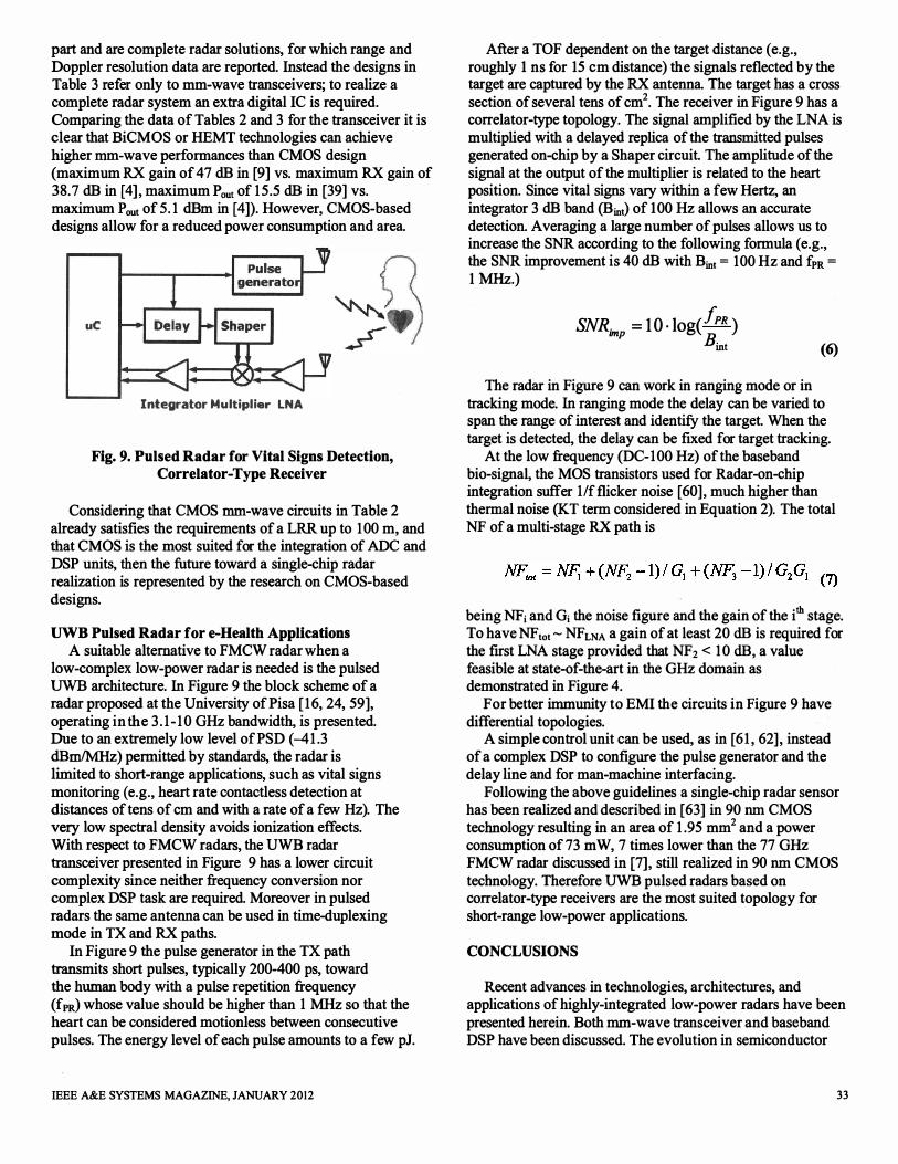
uC
Integrator Multipl ier LNA
Fig. 9. Pulsed Radar for Vital Signs Detection, Correlator-Type Receiver
Considering that CMOS mm-wave circuits in Table 2 already satisfies the requirements of a LRR up to 100 m, and that CMOS is the most suited for the integration of ADC and DSP units, then the future toward a single-chip radar realization is represented by the research on CMOS-based designs.
UWB Pulsed Radar for e-Health Applications A suitable alternative to FMCW radar when a
low-complex low-power radar is needed is the pulsed UWB architecture. In Figure 9 the block scheme of a radar proposed at the University of Pis a [ 1 6, 24, 59], operating in the 3 . 1 - 1 0 GHz bandwidth, is presented. Due to an extremely low level ofPSD (�1 .3 dBmIMHz) permitted by standards, the radar is limited to short-range applications, such as vital signs monitoring (e.g., heart rate contactless detection at distances of tens of cm and with a rate of a few Hz). The very low spectral density avoids ionization effects. With respect to FMCW radars, the UWB radar transceiver presented in Figure 9 has a lower circuit complexity since neither frequency conversion nor complex DSP task are required. Moreover in pulsed radars the same antenna can be used in time-duplexing mode in TX and RX paths.
In Figure 9 the pulse generator in the TX path transmits short pulses, typically 200-400 ps, toward the human body with a pulse repetition frequency (fpJJ whose value should be higher than 1 MHz so that the heart can be considered motionless between consecutive pulses. The energy level of each pulse amounts to a few pJ.
IEEE A&E SYSTEMS MAGAZINE, JANUARY 2012
After a TOF dependent on the target distance (e.g., roughly 1 ns for 15 em distance) the signals reflected by the target are captured by the RX antenna. The target has a cross section of several tens of cm2. The receiver in Figure 9 has a correlator-type topology. The signal amplified by the LNA is multiplied with a delayed replica of the transmitted pulses generated on-chip by a Shaper circuit. The amplitude of the signal at the output of the multiplier is related to the heart position. Since vital signs vary within a few Hertz, an integrator 3 dB band (Bint) of 100 Hz allows an accurate detection. Averaging a large number of pulses allows us to increase the SNR according to the following formula (e.g., the SNR improvement is 40 dB with Bint = 100 Hz and fpR = 1 MHz.)
SNR. = 1 0 . 1og(iPR ) Imp B int (6) The radar in Figure 9 can work in ranging mode or in
tracking mode. In ranging mode the delay can be varied to span the range of interest and identify the target. When the target is detected, the delay can be fixed for target tracking.
At the low frequency (DC-l 00 Hz) ofthe baseband bio-signal, the MOS transistors used for Radar-on-chip integration suffer lIf flicker noise [60] , much higher than thermal noise (KT term considered in Equation 2). The total NF of a multi-stage RX path is
being NFi and Gi the noise figure and the gain of the ith stage. To have NFtot - NFLNA a gain of at least 20 dB is required for the first LNA stage provided that NF2 < 1 0 dB, a value feasible at state-of-the-art in the GHz domain as demonstrated in Figure 4.
For better immunity to EMI the circuits in Figure 9 have differential topologies.
A simple control unit can be used, as in [6 1 , 62] , instead of a complex DSP to configure the pulse generator and the delay line and for man-machine interfacing.
Following the above guidelineS a single-chip radar sensor has been realized and described in [63] in 90 nm CMOS technology resulting in an area of 1 .95 mm2 and a power consumption of 73 mW, 7 times lower than the 77 GHz FMCW radar discussed in [7], still realized in 90 nm CMOS technology. Therefore UWB pulsed radars based on correlator-type receivers are the most suited topology for short-range low-power applications.
CONCLUSIONS
Recent advances in technologies, architectures, and applications of highly-integrated low-power radars have been presented herein. Both mm-wave transceiver and baseband DSP have been discussed. The evolution in semiconductor
33
technologies allows the low-cost and low-power integration of mm-wave radar t ransceiver and DSP unit in the same CMOS chip with performances suitable for several radar applications: automotive, e-health, security, vital signs detection - to name just a few. Since DSP and AID converter are already available as single-chip CMOS solutions we foresee the future migration from single-board radar to single-package or even single-chip radar systems. For SRR operating at several tens of GHz the on-chip integration of the antenna becomes feasible.
The main equations needed to explore the radar design space are presented and used to define the architecture and the main parameters of highly-integrated FMCW and pulsed radars. Two scenarios are analyzed: a 77 GHz automotive LRR using an FFT DSP baseband chain and a low-cost pulsed SRR for e-health applications. The latter works in the 3-10 GHz UWB spectrum, with a correlator-type receiver avoiding the use of a dedicated DSP hardware unit. Recent results achieved when designing in CMOS technology key components of the highly-integrated radar have also been discussed: a low-power threshold-configuring SAR ADC, a pipeline cascade FFT co-processor, mm-wave LNA, and on-chip integrated double-slot antennas.
REFERENCES
34
[ I ] M. Goppelt, H.-L. Blocher and W. Menze, Automotive radar - investigation of mutual interference mechanisms,
Adv. Radio Sci., Vol. 8, pp. 55 - 60, 20 1 0.
[2] D. Hoetzer et aI. , Automotive Radar and Vision Systems - ReadY for the Mass Volume Market,
Vehicle Dynamics Expo, October 2008.
[3] Australian communications authority, RF planning group, doc. SP4/0 1 , A review of automotive radar systems - devices and regulatory frameworks, ApnI 200 1 .
[4] J . Lee, Y.-A. Li, M.-H. Hung, S.-J. Huang, A Fully-Integrated 77-OHz FMCW Radar Transceiver in 65-nm CMOS Technology,
mEE J. Solid State Circuits, Vol. 45, No. 12, 20 1 0, pp. 2746 - 2756.
[5] Mei Li, R. Evans, E. Skafidas and B. Moran, Radar-on-a-chip (ROACH),
mEE Radar Conference, 201 0, pp. 1224 - 1 228.
[6] M. Jahn, A. Stelzer and A. Hamidipour, Highly integrated 79, 94, and 120-OHz SiGe radar front-ends,
mEE MTT-S Inter. Microwave Symp., 201 0, pp. 1 324 - 1 327.
[7] T. Mitomo et aI. , A 77 GHz 90 nm CMOS transceiver for FMCW radar applications,
IEEE J. Solid State Circuits, Vol. 45, No.4, pp. 928 - 937, 201 0.
[8] E. Ragonese, et aI., A fully integrated 24 GHz UWB radar sensor for automotive applications,
IEEE ISSCC 2009, pp. 306 - 307.
[9] L. Moquillon et aI., Low-cost fully integrated BiCMOS transceiver for pulsed 24-OHz automotive radar sensors,
mEE CICC 2008, pp. 475 - 478.
[ 1 0] V. Winker et aI., 79 GHz automotive short range radar sensor based on single-chip SiGe-transceivers,
EuRAD 2008. pp.459 - 462.
[ I I ] M.D. Richter et aI., 77 GHz automotive digital beamfonning radar with SiGe chipset,
Germsn Microwave Conf. 201 0, pp. 210 - 2 1 3 .
[ 1 2] V . Jain et aI., A single-chip dual-band 22-to-29GHzI77-t0-8 IGHz BiCMOS transceiver for automotive radars,
IEEE ISSCC 2009, pp. 308 - 309, 309a.
[ 1 3] T. Nagasaku et aI., 77GHz Low-Cost Single-Chip Radar Sensor for Automotive Ground Speed Detection,
IEEE CISC'08, pp. I - 4.
[ 1 4] E. Huyn et aI., Design and implementation of automotive 77GHz FMCW radar system based on DSP and FPGA,
IEEE ICCE 20 1 1 , pp. 5 1 7- 5 1 8.
[ 1 5] Sang-Dong Kim et aI., Design and implementation of a full-digital pulse-Doppler radar system for automotive applications,
mEE ICCE 20 1 1 , pp. 563 -564.
[ 1 6] D. Zito, D. Pepe, B. Neri, D. De Rossi, A. Lanata, A. Tognetti and E. Scilingo,
Wearable System-on-a-Chip UWB Radar for Health Care and its Application to the Safety Improvement of Emergency Operators,
mEE EMBS 2007, pp. 265 1 - 2654.
[ 1 7] Changzhi Li, Xiaogang Yu, Chien-Ming Lee, Dong Li, Lixin Ran and Jenshan Lin,
High-Sensitivity Software-Configurable 5.8-OHz Radar Sensor Receiver Chip in 0. 1 3 -J.IID CMOS for Noncontact Vital Sign Detection,
IEEE Trans. Microwave Theory and Techniques, Vol. 58, No. 5, 20 1 0, pp. 1410 - 1419.
[ 1 8] Changzhi Li, Xiaogang Yu, Dong Li, Lixin Ran and Jenshan Lin, Software configurable 5.8 GHz radar sensor receiver chip in 0. 1 3 I'm CMOS for non-contact vital sign detection,
IEEE RFIC 2009, pp. 97 - 1 00.
[ 1 9] Yeo-Sun Yoon et aI. , MVDR Beamfonning for Through-the-Wall Radar Imaging,
mEE Aerospace and Electronic Systems Magazine, Vol. 47, No. I , pp. 347 - 366, 20 1 1 .
mEE A&E SYSTEMS MAGAZINE, JANUARY 20 1 2
[20] A. Dallinger et aI. , Coherent millimeter-wave imaging for security applications,
IEEE Radar Conference 2007, pp.28 - 3 1 .
[2 1 ] N . L'Insalata, S . Saponara and L. Fanucci, Automatic synthesis of cost effective FFTIIFFT cores for VLSI OFDM systems,
IEICE Trans. on Electronics, Vol. E9 1C, No. 4, pp. 487 - 496, April 2008.
[22] S. Saponara and L. Fanucci, VLSI design investigation for low-cost, low-power FFTIIFFT processing in advanced VDSL transceivers,
[23] A. Fonte et aI., 6O-GHz Single-Chip Integrated Antenna and Low Noise Amplifier in 65-run CMOS SOl Technology for Short-range Wireless Gbits/s Applications,
IEEE Applied Electronics 201 1 .
[24] D . Zito, D . Pepe, B . Neri, D . De Rossi and A . Lanata, Wearable System-on-a-Chip Pulse Radar Sensors for the Health Care: System Overview,
IEEE AINAW 2007, pp. 766 - 769.
[25] S. Saponara, L. Fanucci, P. Nuzzo, C. Nani and G. Van der Plas, Architectural Exploration and Design ofTime-interleaved SAR Arrays for Low-Power and High Speed AID Converters,
IEICE Tran. on Electronics, Vol. E-92C/6, pp. 843 - 852, 2009.
[26] S. Saponara, Configurable Array of Low-complex SAR ADCs,
Analog Integrated Circuits and Signal Processing, Vol. 67, pp. 103 - 1 07, 201 1 .
[27] S . Montusclat, F . Gianesello and D . Gloria, Silicon integrated antenna substrate benchmarking for MMW wireless applications in advanced CMOS technologies,
EuCAP, 2006, p. 680.
[28] E. FishIer, et ai, MIMO radar: an idea whose time has come,
IEEE Radar Conference, 2004. pp. 71 - 78.
[29] S . Gogineni, et aI., Monopulse MIMO Radar for Target Tracking,
IEEE Trans. Aerospace and Electronic Systems, Vol. 47, No. 1 , 201 1 , pp. 755 - 768.
[30] G. T. Pratt, Subspace Optimization in Centralized Noncoherent MIMO Radar,
IEEE Trans. on Aerospace and Electr. Syst., Vol. 47, No. 2, 201 1 , pp. 1230 - 1 240.
[3 1 ] E. Grossi et aI., Robust waveform design for MIMO radars,
IEEE Trans. on Signal Processing, 201 1 .
[32] F. Baronti et aI., Design and Verification of Hardware Building Blocks for High-Speed and Fault-Tolerant In-Vehicle Networks,
[39] Dong Min Kang et aI., A 77GHz Automotive Radar MMIC Chip Set Fabricated by a 0 . 1 5 IlIll. MHEMT Technology,
IEEE IMWS, pp. 2 1 1 1 - 2 1 14.
[40] A. Komijani et aI., A 24-0Hz, 14.5-dBm fully-integrated power amplifier in O. l 8 1lIll. CMOS,
IEEE J. Solid-State Circuits, Vol. 40, No. 9, pp. 1 90 1 - 1 908, September 2005.
[41 ] T. La Rocca et aI., 60 GHz CMOS amplifiers using transformer-coupling and artificial dielectric differential transmission lines for compact design,
IEEE J. Solid-State Circuits, Vol. 44, No. 5, pp. 1 425 - 1435, May 2009.
[42] T. Yao et aI., Algorithmic design of CMOS LNAs and PAs for 6O-GHz radio,
IEEE J. Solid-State Circuits, Vol. 42, No. 5, pp. 1 044 - 1 057, 2007.
[43] T. Suzuki et aI., 60 and 77 GHz power amplifiers in standard 90 run CMOS,
IEEE ISSCC, February 2008, pp. 562 - 563 .
[44] M. Seo et aI., A 1 . 1 V 1 50 GHz amplifier with 8 dB gain and 6 dBm saturated output power in standard digital 65 run CMOS using dummy pre-filled microstrip lines,
IEEE ISSCC 2009, pp. 484 - 485.
35
36
[45] D. Shaeffer et aI., A 1 .5-V, 1 .5-OHz CMOS low noise amplifier,
IEEE J. Solid-State Circuits, Vol. 32, No. 5, pp. 745 - 759, May 1 997.
[46] A. Ismail et aI., A 3-1 0-OHz low-noise amplifier with wideband LC-ladder matching network,
IEEE J. Solid-State Circuits, Vol. 39, No. 1 2, pp. 2269 - 2277, December 2004.
[47] E. Adabi et aI., 30 GHz CMOS low noise amplifier,
in RFIC Symp. Dig., June 2007, pp. 625 - 628 .
[48] B Ashfar et ai, A robust 24 mW 60 GHz receiver in 90 nm standard CMOS,.
IEEE ISSCC, pp. 1 82 - 1 83 , 2008 .
[49] R. Berenguer et aI., A 43.5 mW 77 GHz receiver front-end in 65 nm CMOS suitable for FMCW automotive radar,
IEEE CICC 201 0, pp. 1 - 4.
[50] D. Chowdhury et aI. , A single-chip highly linear 2.4 GHz 30 dBm power amplifier in 9O nm CMOS,
IEEE ISSCC 2009, pp. 378 - 379.
[5 1 ] P. Haldi et aI. , A 5.8 GHz 1 V linear power amplifier using a novel on-chip transformer power combiner in standard 90 nm CMOS,
IEEE J. Solid-State Circuits, Vol. 43, No. 5, pp. 1 054 - 1063, 2008.
[52] S.K. Alam, A Novel 2.4 GHz CMOS Variable Gain Low Noise Amplifier Design for Bluetooth and Wireless LAN Applications,
IEEE ICCE 2007, pp. 1 - 2.
[53) S. Wang and B.Z. Huang, A high gain CMOS LNA fro 2.4/5.2 GHz WLAN applications,
Progress in Electromagnetic Research, Vol. 2 1 , pp. 1 55 - 1 67, 201 1 .
[54) S. Saponara et aI., Performance and complexity co-evaluation of the advanced video coding standard for cost-effective multimedia communications,
EURASIP Journal on Applied Signal Processing, Vol. 2004, No. 2, pp. 220 - 235, 2004.
[55) F. Vitullo et aI. , Low-complexity link microarchitecture for mesochronous communication in Networics-on-Chip,
IEEE Trans. on Computers, Vol. 57, No. 9, pp. 1 196 - 120 1 , 2008.
[56) S. Saponara et aI., Algorithmic and architectural design for real-time and power-efticient Retinex image/video processing,
J. Real-Time Image Processing, Vol. 1 , No. 4, pp. 267 -283, 2007.
[57] S. Saponara et aI., Application-specific instruction-set processor for Retinex-like image and video processing,
IEEE Trans. on Circuits and Systems II, Vol. 54, No. 7, 596 - 600 , 2007.
[58) S. Saponara et aI., Dynamic control of motion estimation search parameters for low complex H.264 video coding,