Page 1
reliable high precision converter for use in particle accelerators. OCR Output
elements of a power converter which will lead us to a regulation topology having all the qualities required of a
obliged to limit the content of this course. Our objective therefore is to follow a rapid overview of the various
The domain of regulation as well as the numerous methods of analysis being vast [l, 2], we have been
the fundamental building blocks of the regulation system no longer form the limiting factor of performance.
the lower performance of the former elements. Further, the elements such as operational amplifiers etc, used as
Hence, a particular attention should now be paid to the regulation loops which were previously masked by
DCCI`, once again fuliil our requirements.
Likewise the current transducers have followed a similar ¤·end and, along with the galvanic isolation of the
applications.
analogue converters, which have greatly improved over the last years and can now fulfil most of our
The references of the potentiometer type driven by up-down motors have been replaced by digital to
the regulation circuits.
the current transducer;
the reference source;
The elements concerned most directly with these objectives and more importantly towards the precision are:
fundamental objectives, other than electrical problems, have always been the precision and the reliability.
decades. Whether it be conventional equipment or the more modem generation of power converters the
In the domain of accelerators, power converter performance has progressed notably during the last two
converter is also described.
specification requirements. A novel regulation principle for a series-connected power
control synthesis is applied using various approaches generated by the different
system is defined. This leads us to a cascaded voltage loop and current loop, on which
on the above, as well as the specification and measurement problems, the control
described. From the electrical model, operational characteristics are deduced. Based
'Ihe power properties and design criteria of a power converter feedback system are
CERN, Geneva, Switzerland
A. Beuret
- gg
Page 2
and the load [3]. OCR Output
elements concemed in the command process, i.e. the thyristor bridge including its transformer, the passive filter
Before going onto the regulation, we should first consider the characteristics of the three fundamental
2.2 Operation
Fig. 2 Filter module Fig. 3 Equivalent diagram of a magnet load
-··il-—····· -l¤·
···it ·····—·l¤·
order, and of any type (e.g. thyristor control or switch mode).
consideration. While the load is always the last element, the other series—connected elements can be in any
of the latter (Fig. 3). Other parasitic effects such as capacitance to eanh may need to be taken into
The load consists of a connection between the convener and its load as well as the resistance and inductance
in figure 2 or a simple LC filter.
The filter must reduce the residual ripple to an acceptable level for the user. lt is normally of the type shown
suitable firing circuit.
The regulation and rectification can be carried out by a phase controlled thyristor bridge driven by a
galvanic isolation.
Adaptation of the network to the user needs is normally carried out using a transformer which also provides
Fig. 1 Block diagram of a power converter
mu necririen *-¤¤¤
”E“'°'*‘ Aomrnion l....l ‘f°°E,,'g;§}‘°" l..._l•=1ttzn l._l usan
We can sub—divide the power convener into four principle blocks
2.1
- gl
Page 3
Fig. 5 Static characteristic of the bridge OCR Output
c¤· s0· l20‘°‘
%`/ CONDUCTIONDISCONTINUOUS
S0'I•
/·jVp:T‘;_V¤cos¤1WO'/•
function of ot to Vp is therefore non-linear.
This characteristic is shown in figure 5 which shows the case of discontinuous conduction. The transfer
Fig. 4 Bridge output voltage
DU . OUJ 1\ _ -0 anglz Hh
I, I . \ Il . \ ll \\ I 'I I \I\ \’ 1 ·1 ’ \ [ \ \ I [ I [ l l \[ |\[ I I \
' Y ' I \ 1 l l \l lI? I1 lI I\ ` ’
»»t I ll I I \\ ’>> \l’ \ l \4\ ’ ";>\’/"’¤I'>""`/"lw / ’_`r/’_ "» / ’_"" ` /Va Va.t Vs.z
(1)VP = ms otg
network, the average DC output as a function of the firing delay ot is given by
Consider figure 4 which shows the output of a full-wave thyristor bridge. In the case of a balanced
2.2.1
- 82
Page 4
Fig. 6 Closed-loop firing circuit of a thyristor bridge
c) BDDE DIAGRAM
I . I I I I I l
I tm
Praia
m nt. T I IIhI i ' 1 g I IMI II ,|I III I I I I I " I . I OCR Output
`I`Te for r~~“`°“’
D) STATIC CHARACTERISTIC
INSTABILITY AREA
al BLOCK DIAGRAM OF A CLOSED-LOOP FIRING CIRCUIT AND A THYRISTDR BRIDGE
/ LJ
BRIDGE
mp · ?`m¤¤¤I?.I ,§§I§§,I I ; I_I_IVe ...I f H
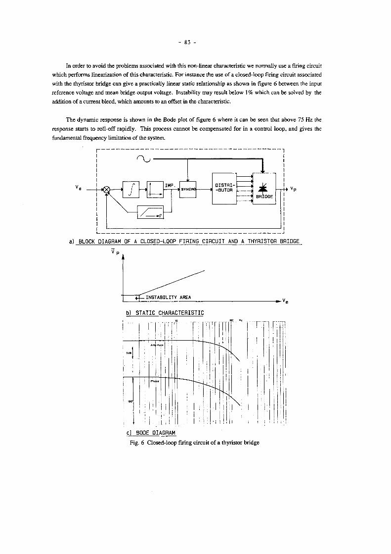
fundamental frequency limitation of the system.
response starts to roll—off rapidly. This process cannot be compensated for in a control loop, and gives the
The dynamic response is shown in the Bode plot of figure 6 where it can be seen that above 75 Hz the
addition of a current bleed, which amounts to an offset in the characteristic.
reference voltage and mean bridge output voltage. Instability may result below 1% which can be solved by the
with the thyristor bridge can give a practically linear static relationship as shown in figure 6 between the input
which performs linearization of this characteristic. For instance the use of a closed-loop firing circuit associated
In order to avoid the problems associated with this non-linear characteristic we normally use a firing circuit
Page 5
21: 300.C OCR OutputR S (6)e.g. R S 59 mf!
ESR) does not hinder the correct operation of the filter, i.e. gives a zero in equation (2) above 300 Hz.
We no longer need a damping resistor but must make sure that any parasitic resistance (e.g. connections, capacitor
—- . . L (21: 20)“° g 3 mH, C = 9 mF (5)1 LC = —For the filter at 30 Hz, we have
which is half the mathematical critical damping.
e. g. R 0.58 QR = J;
A reasonable value of damping is given by
. . L ° g 1 mH, C = 3 mF (3)LC = +-· (zu 90)*
For a filter at 90 Hz, we have
VP (s) l + RCs + LCs(2)
V! (s) _ 1 + RCs
function
The load impedance can be ignored compared with the output impedance of the filter giving a transfer
band pass limit of 75 Hz.
consider the case of an LC filter at 90 Hz and 30 Hz used on the output of a 6-pulse thyristor bridge having a
very attractive if we can choose a filter below the bandwidth limit of the system. To illustrate this we will
Once the introduction of a passive filter is necessary, it is evident that the ratio attenuation/price becomes
The large damping resistor is no longer needed leading to further economies.
can be achieved. Hence, the filter can be undamped which will give higher attenuation with no extra cost.
2) place the resonance of the Hlter sufficiently below the limit of the command element such that compensation
adding a damping resistor and eventually a second C and the attenuation may not be sufficient;
correct damping cannot be achieved electronically. Therefore, the filter may need to be damped elecuically by
a thyristor bridge). The consequences are that no compensation can be obtained for the filter and in particular
1) place the resonance of the filter above or close to the frequency limit of the command element (e.g. 75 Hz for
tolerated by the load. We have two possibilities :
The parameters, resonant frequency and damping, of the passive filter are dictated by the residual ripple
2.2.2
- 84
Page 6
overshoot. OCR Output
following error;
perturbation error;
long-term drift;
resolution;
precision;
The following are the points of particular interest from a point of view of the closed-loop control
3.1
we need and the specification of the power converter itself [4, 5].
loop control system. However, we must also take into consideration the quality of the various feed-back signals
Having defined the fundamental elements of the system, we can now consider the structure of a closed
3. STRUCIUBE OE 'IHE CLOSED-LOOP SYSTEM
tum caused by a cooling pipe can require a higher-order model.
result due to saturation of the magnetic circuit. In certain cases coupling with the vacuum chamber or a shorted
simple since it is normally a first-order element (0.1 < 1 < 100 s). However, a non—linear characteristic can
The load is the most important element of the system since it dominates the specification. Its make up is
2.2.3 Qad
Fig. 7 Bode plot of filters
Frequency In It10 100
-40.
_gg [ ...,...., . .......
-20 .
-10.
30Hz FILTER
»90Hz FILTER
10.
Db
Ga I n
this improvement for a cost increase of about 3.
Looking at the Bode plots of figure 7, we can see a difference of attenuation of 35 dB (factor of 56) at 300 Hz;
- gg
Page 7
signal. These two effects are illustrated in figure 9. OCR Output
found. The limiting performance for us is the induced noise into the primary bus-bar and noise on the output
is a zero-flux type of DCCl` (Direct Current Current Transducer) although the older Hingorani type can still be
rejection. The performance of the system depends to a large extent on this element. The most usual device today
Current measurement influences directly the precision, long·terrn drift and to a lesser extent the perturbation
3.2 Current measurement
requirements in this sense.
The overshoot specification comes from the hysterisis limits of the magnet as well as the obvious beam
loops.
The following error is only applicable to a dynamic change and depends entirely on the quality of the
Fig. 8 Illustration of the precision long-term drift and perturbation error
DRIFT
r¢n*runnArxou I E%OR L¤4O TERMREFERENCE
NUHERI C I Innzcxuou
rejection. This is often the most usual reason to add an active filter.
is the random mains perturbation which has low-frequency components for which the passive filter has little
rejection for this type of perturbation. If this is not the case, we may need to add an active filter. Secondly, there
chopping the 3-phase mains current to form the bridge output. In general the passive filter has sufficient
The perturbation error is the most critical point. Firstly there is the continuous ripple resulting from
transducer and to a lesser extent those of the regulation electronics.
The long-term drift depends essentially on temperature and ageing effects on the reference and current
influence the resolution.
The resolution depends essentially on the reference, since the rest of the process has no element likely to
reference and the current transducer which must not be degraded by the control loops.
The precision defines generally the absolute tolerance of the current. lt relies on the quality of the
- ..
Page 8
shown in figure ll, photos a and b. OCR Output
The typical effects of a mains perturbation and that of the current transducer on the output voltage are
the load.
the current transducer;
the mains network;
The perturbations come from three sources :
Fig. 10 Block diagram of control process and perturbations
*’EF*T°’¤*TI¤¤ nanrnksiruts nennmarruusmmm; iiiimr
I/P—•1 crr;cnt;r)1éEw¤Ii.|F1tran I..|•.0A¤ }..• 0/P
likely to create a fluctuation of the output current.
The block diagram (Fig. 10) represents the principle elements of the control process and the perturbations
3.3 E lsian
while the basic concept gives a far superior performance.
The electronics employed in the zero—flux type now give a comparable reliability to the older Hingorani type
The zero—tlux type offers better performance in both these domains.
bandwidth such as an active filter.
The induced noise in the bus—bars can only be eliminated by including it within a loop of sufficient
the bandwidth of the system.
The noise on the signal is particularly annoying since it will appear throughout the control process within
Fig. 9 Hlustration of secondary effects of the current transducer
cunnenr rimswcan
if-- nun: II + V ' ‘ '
REFERENCE .t.6?t_.I svsrsn LA...§;
irtnrtnunxou I A
- gy
Page 9
Fig. 12 Bode plot of filter and magnet OCR OutputFrequency ln Hz
10m 100m 1000m 10 100 1000-40.00
-20.
MAGNET
-10.
FILTER
10 .
Db
Gai n
the magnet is given.
In order to resolve this problem, we would look at figure 12, where the typical analysis of a filter as well as
2) measure the voltage on the output and correct at the input.
1) measure the current and correct at the input;
The rejection of the mains perturbations as seen on the output voltage can be achieved in two ways
coupling with other sources.
The perturbations introduced by the load are mainly due to resistance variations but can also be due to
Fig. ll Perturbation effects on the output voltage
transducerPhoto a — Transient perturbation of 2.5% Photo b — Pcrturbation duc to Hingorani currcnt
—.* t
_______Il-llll llIIIIJ I i IIM, Wilma
IlIHh'“
- 88
Page 10
between the reference (u) and the output (y) by adjusting the regulation parameters of the compensation. OCR Output
In general, for the type of control that interests us as shown in figure 14, we wish to minimise error
4.1
respected.
supplied by the previous voltage source. 'I`hus the rules of cascaded voltage and current sources are rigorously
Likewise the compensation of the current loop associated with the load inductance forms a current source
near perfect voltage source at the output terminals.
The compensation of the voltage loop generates a command signal for the firing system thus producing a
Fig. 13 Principle block diagram of the control system
PEnTunaAT1oNs
cunr·tENT THANSDUCER- _‘'`'`"‘‘‘“
IPERTUHBATIONS INOISEI MAIIIS I PERTURBATION
to-wnrston ' v °UmEN° u E mm ¤ R
I cmcurt II Frame I
c0MPENsAr1oN
v0LTAGE Loop
COMPENSATION
cunnsut LOOP
nEFEnENcE
(voltage loop) and the output current (current loop).
Together this leads to the principle diagram shown in figure 13 where we control the output voltage
establish the low frequency command of the system as well as the rejection of the load perturbations.
However, the current being the main control parameter, it is from the current transducer that we shall
required information.
measured rather than correct a secondary effect. In particular, a simple voltage divider can be used to provide the
In simpler terms it appears evident that one should correct the source of the perturbation as soon as it can be
ratio.
from the output voltage is much more interesting particularly when we take into consideration the signal-to-noise
bandwidth above the magnet break-point. Hence, the second method consisting of generating a correction signal
It is evident that the infomation contained in the voltage is much richer than that of the current for
Page 11
we can see that the bandwidth has practically doubled while the damping factor has increased to the desired level. OCR Output
(PI) compensator associated with a phase advance will give the required performance as seen in figure 16. There
autonomous way. If the passive filter has a minimum damping factor of 0.2, then a proportional integrator
Since the load is decoupled, we can simply consider the thyristor bridge and passive filter in an
performance criteria we have chosen.
The objectives of the voltage loop are to provide satisfactory mains rejection while preserving the dynamic
4.2
(C) or 0.5 [2].
minimize ISE. For a second order system this leads us to maximize the pulsation, (0)) and to a damping factor
In an ideal case ISE = 0, but in reality ISE is always greater than zero. We need a compensation which will
Fig. 15 Error evolution
perturbation at t= tp.
where e(t) represents the error as shown in the shaded area of figure 15, with a step input introduced at t = 0 and a
(7)ISE = | c‘ (t) dt
(ISE) defined as
responses of different compensations. In this respect we have chosen to minimize the integral squared error
can be easily observed by the step response of the system, we have chosen this method to compare the relative
is therefore important to assure that this is adequate by a choice of compensation. Since the dynamic behaviour
The behaviour of the system in relation to perturbations is govemed principally by its dynamic response. It
Fig. 14 Block diagram of a closed-loop system
compewsurou ii_.]SYSTEM l..r..• Vu LQ;
- gg
Page 12
(ll)X(t) = (C + D K)- X(t) + D E (t) OCR Output
(10)dX/dt = (A+ BK)- X(t)+ BE(t)
The state equation of the compensated system is
The matrix K is called the feedback matrix and has a dimension of p n.
(9)U(t) = E(t) + K X(t)
system. The principle of the state feedback uses a law of the form
The matrix A is the dynamic matrix of the system. Its eigen values characterize the dynamics of the
and (A, B, C, D) are the state matrices of the system.
Y(t) is the output vector of dimension q,
U(t) is the input vector of dimension p,
X(t) is the state vector of dimension n,
where
(8)Y(t) = C X(t) + D U(t)
dX/dt = A X(t) + B U(t)
Consider a linear system represented by a state model inthe form of :
4.2.1 State feedback
feedback compensation, the principles of which will be recalled.
its superior attenuation, then this type of compensation becomes insufficient. We would then tum towards state
However, if we wish to achieve the same performance from an undamped filter, which has been chosen for
Fig. 16 Comparison of performance with and without voltage loop
Photo a - Step response with voltage—l0op Photo b - Step response without voltage-loop
——~—•t
ann-nn:-n !IIlIIIIII 1;1jj1i1Z1IUMIIIIIIII IIIIIIIIIIIIIIIIIIIIIII-IIIIIIIIIIIIIIIIIIHIIIIIIIIIIIEIIIIIIIIILVIIIIIIIIIII-EIIUI
nn- nnnnnn Il nllinnnn IIIMIIII-IIIIIIIIIIIII Vs
+F ILTEFRITVe Fxnxuc ys‘V° + •° c0M»=ENsAT10N +';IFiI'g Ys
-91
Page 13
é%(,)A B K = " _ -+*5 k—lR/L 14 ( ) OCR Outputk,/L (k2—1)/L
The dynamic matrix of the system becomes
(13)vp=u+Kx=U+[k,k,][1v,]
We then define a state feedback applying a law of the form
(12)dI /dt 0 -1/ L I 1/ L = + dVL/dt 1/C —R/L VL R/LIt can be represented by
Fig. 17 Passive filter
H T VL
L ‘ { IC
In order to illustrate the use of state feedback, we will consider the passive filter of figure 17.
4.2.2
dynamic compensators) [2, 9, 10].
However, there exists certain methods of deriving these from the input and outputs of the system (observers and
There exists a number of cases where all the states of the system are not available or measurable.
B and (A+B- K).
The matrix K can be determined in a systematic way (hence simply programmed) from a knowledge of A,
mode of the closed system [6 - 8].
One can show that the idea of govemability of a system is equivalent to the ability to arbitrarily choose the
improve the stability and the dynamics of the system.
The new dynamic matrix is thus A + B - K. It can be seen that the correct choice of the matrix K will
- ..
Page 14
Fig. 18 Block diagram of the voltage loop
FT?+ Ta
c p,....v5 OCR Output"·+ »=.r. l..:.m¤LJ ¤ l;@:;{f +
shown in figure 18 and the performance thus obtained in figure 19.
compensator in the feedback which gives a filtering effect seen from the reference. The system is therefore
not wish to deteriorate the dynamics of the system, we have chosen to introduce a small phase advance
temporarily lost. In order to remedy this situation we can introduce a slowing down of the system. Since we do
reference. In this case, we fall on the limit of linear operation of the thyristor bridge, and the voltage source is
small signal operation. However, our system must be able to respond to large amplitude signals from the
While the above reasoning has not taken into account the thyristor bridge, this is of little importance for
shown that it is more interesting to introduce a proportional action instead of the state feedback kg.
does not eliminate the static error. For this we must add an integral action on the output voltage. Reality has
are difficult to measure. Although this type of correction can determine the dynamic properties of the system, it
For our example, we can take the capacitor current and the output voltage as state variables neither of which
kl - 4 R — QL {x/glgiving:
we would like to double the bandwidth, we would have kg = -3, and we can choose the damping factor Q this
from which we can see the possibility of adjusting the resonant frequency and the damping factor. For instance if
(15)L1 - k2 1 — k2-?-s°+ RC——l£ s+1=0
Thus we deduce the characteristic equation
- gg _
Page 15
10 Hz and 20 dB at l Hz can be seen. OCR Output
when the active filter is used also to increase the low-frequency gain of the system. An improvement of 50 dB at
shows the addition of the active filter purely as a filtering element. The curves (c) and (c') show the rejection
the successive improvements made when adding an active filter. The curve (a) has no active filter. The curve (b)
resultant single input system with increased bandwidth. The rejection curves shown in figure 22 demonstrate
vector of the filter, generates the command for the two inputs in a manner to render the two compatible and give a
This leads to the structure shown in figure 21. The vital element is the feedback matrix K which, from the state
increase the performance of the system at the lower frequencies where the passive filter has little or no effect.
for introducing the active element are not only to reduce the residual ripple but perhaps more importantly to
The system now has two inputs which demands a different strategy to that used previously. The reasons
developed around the system shown in figure 20.
structure is a vast subject which we will not coverin detail. We will however consider the general principles,
reached we must introduce an active element [11]. The choice of the active element as well as its command
There are limits to the performance that can be achieved with a passive filter alone and once these are
4.2.3 Introduction of an active filter
Fig. 19 Performances of voltage loop
(large signal)(small signal)Step response of closed voltage loopStep response of closed voltage loop
§10m$ itoms
Step response of filter with state feedbackStep response of filter
- g4
Page 16
Fig. 22 Rejection curves OCR Output
,*'°!"°"¢ `‘`` l—+—-—l--+—l—e~·i —<v4 MT‘+ii‘i"ii‘§‘*
`lg". T ` L Tr"‘i·%0dB*F"|"*I·r
M LYYiY¥*°'”m
~+#l~··l·-l·l·l;%+%·+->l*—··
;;l2;1%L;zA;.;i;;.ett;;;t;t:t»ti4i
Fig. 21 Voltage loop with active filter
FILTER
P IVe +PASSIVE
"°‘
Fig. 20 Active clcmcnt in thc capacitor branch
ROTECTIDN
- 95 ..
Page 17
effect in practice is very small, since the rate of change of resistance is small for most magnets. OCR Output
temperature, following a step-change in current, the simple integrator cannot reject this completely, although the
Concerning the rejection of resistance change of the load, it should be noted that during a change of
interesting compromise.
consideration these points, practical experience has shown that a bandwidth of a few Hertz represents an
the reference source noise, it is clear that the slower the system the less will be its influence. Taking into
use of a zero-flux transducer has shown that in most cases it represents no limitation for the system. Concerning
The influence of the current transducer noise depends on the gain of the system at the noise frequency. The
the closed voltage loop.
Conceming the interference with the voltage loop, we should maintain a margin of about one decade below
what type of regulation should we adopt to minimize the oveishoot to a step input
how to reject the resistance changes of the load and cope with the inductance changes;
c) noise from reference source, particularly if it is not close to the control loop;
b) noise injection from the current transducer;
a) interference with the voltage loop;
the bandwidth required in the current loop to avoid
The main points to take into consideration in this case are
The current transducer is included with the load as well as its intemally generated noise.
Fig. 23 Block diagram of current·loop
•Lu01ss
c0•»zrsAt1¤Nl7 some:nar. _Q Jumnn n.¤0•¤| |v0t.1*Asa |,,;;> _| tom +
represented by the block diagram of figure 23.
In this case a zero static error is needed which can be obtained by a PI compensator. The system could be
4.3.1
In the two cases the precision obtained is the main objective.
acceleration.
2) the convener used in an accelerator where, as well as the static requirements, it must ramp during
1) utilization of the convener in a static state (Beam transfer, Hat-top operation);
the current loop we need to consider two distinct modes of operation
We have thus obtained, one way or the other, a suitable voltage source as input to our current loop. For
4.3
- 96
Page 18
on that reference. It also gives minimum and maximum operating levels of the voltage source. OCR Output
The limiter is a non-linear element with two thresholds responding only to large reference changes and acting
Fig. 25 Block diagram of current loop with limiter
SOURCEFILTER I GOMPENSATIUN VOLTAGE LOAD
—·REF. + '
LIMITER
diagram shown in figure 25.
This method, associated with a limiter to avoid saturation during large reference changes, leads to the block
easily removed for dynamic tests.
2) The second solution is inspired by the first but consists of a filter introduced in the reference which can be
test may not be seen.
This method has the inconvenience of hiding the closed-loop systems such that any instability during a step
main mode will be the one of the pole and therefore the overshoot problem will be solved.
If the bandwidth of the closed-loop system is large compared to the position of the pole, it is evident that the
Fig. 24 Introduction of a zero in the feedback
1+Ts
_ _] + O A 4 + aq | A (1+Ts) _____ L_I 1+Ts _
to avoid noise at the summing point. The resulting process is shown in figure 24.
This is equivalent to placing a filter on the reference. However, this must be associated with a pole in order
1) introduction of a zero in the feedback of the compensation.
The problems of overshoot can be resolved principally in two ways
- gy ..
Page 19
complication of double integration may not be justified. OCR Output
may well dictate which is to be used. If this time is short compared with the transient periods, then the added
In choosing between single or double integration the time during which steady-state ramping takes place
produce a non—negligible variation of this error.
the load. Any change of components will therefore modify the following error and resistance changes will also
where K is the gain of the open loop which is a function of the compensation components and the resistance of
Er = ;
since a simple integration gives a following error of :
constraints on the current transducer, reference source and other noises. The double integration is necessary
The increase of bandwith can only be achieved to the detriment of noise, which puts more severe
the previously added reference filter needs to be removed unless we can assure its high precision.
These two points will introduce new stability problems as well as different transient behaviour. Of course
introduction of a double integration to give zero steady state following error.
increase of the bandwidth to a maximum possible in order to reduce transient times;
constraints as a result of the problems involved in following a dynamic reference [12]. For the current loop these
Concerning the utilization of a power convener in an accelerator, it may be necessary to modify the static
4.3.2 The ratriviri
Fig. 26 Performance evaluation
and filterwithout limiter and filterPhoto b - Response to large step with limiterPhoto a — Response within the linear domain
I__II__H _IIllllll II IllulllmllIIIIIIIII
””'IllE&¤llIIIIIIIII
IIIHLSIQI Eiiiiiiiii
The performance obtained with this type of system is shown in iigure 26.
- gg
Page 20
the liaison element by taking the necessary information where it exists naturally. That is to say the current in the OCR Output
digital transmission of references to the slave elements generally results in a non-linear system. We can eliminate
choice of liaison element becomes critical from both a technical and economic point of view. The solution of
Once the distances between the master and slave converters becomes large (e.g. 14 km in LEP), then the
In fact, only the gain is modified by the number of power converters.
current compensator is the same as a single system.
liaison element (cable, communication system, etc). If the latter is ideal, then the resulting system seen by the
The current compensator drives in parallel the slave voltage sources, which we consider to be ideal, via a
Fig. 27 Block diagram of master-slave with liaison element
MASTER
DCCT
DIVIDER
I LOOP LOOP CONVERTER I I VOLTAGE I+I ICURRENT I T +.I<>t IVDLTAGE Powan lvm I T
DIVIDER
I CONVERTER ‘votr`A's`_IEI ELEMENT I I LOOP ' IgV I POWER I 9.I I SLAVE LIAISON I ,,<>\ IVOLTAGE I
therefore obliged to consider the type of structure shown in Hgure 27.
It is evident from the most elementary rules that the regulation of each unit in current is prohibited. We are
dipoles and quadrupoles in order to distribute the power and limit the voltage to earth.
around the circumference of a machine [13]. Such a connection is frequently found in the chains of the principle
We will consider in this part the control of several power converters placed in series, via their loads,
knowledge of the system and the desired output function.
reference source in order to generate the appropriate signal to eliminate all these errors, calculated from the
The ideal method that one could suggest to eliminate this type of problem is to act numerically on the
filter cannot be taken into account in a systematic way.
the ramp is started. However, the changes in the following error caused by the changes in the components of the
Under these conditions we introduce a following error which we can compensate by modifying the time at which
In the case of a dynamic reference, the problems of overshoot can be resolved by the methods used before.
4.3.3 Qyszrshmt
- gg
Page 21
input to the master converter shares the static and dynamic characteristics between all converters. OCR Output
The problem we have to resolve is whether we can compensate the slave converter in such a way that the
transfer function of the current loop compensator.
transfer function of the voltage source of the master
Hi [1, .. n - 1] : transfer function of slave voltage sources
kg [l — n] : current transducer gain
transfer function of the load
Fig. 29 Function diagram of 'n' power converters
-lx+__I';I;`l Vc IH" IUn+ §é+ U1 IH
x ui xl H 1 I——I " 1
/` T
Hn-1 I·—I k n-1U - n 1
represented by the functional diagram of figure 29.
The system composed of 'n' power converters in a configuration of master-slave without liaison element is
mpensatiortDetermination of
Fig. 28 Block diagram of master-slave without liaison element
MASTER
DCCT
DIVIDER
LOOPPQ I LOOP I CONVERTER I I I VOLTAGE |+| ,,0, I CURRENT I +,,<>t [VOLTAGE POWER IV FUI T
DIVIDER
• LOOP I IVb"ft AGE CONVERTER I I II vouma SI-AVE 1 I IPOWER VeI
I ,.I DCCT
necessary compensation needed for each slave power convener.
series-connected magnet. This leads us to a block diagram as shown in figure 28 from which we will derive the
- 100
Page 22
dynamic role for the entire load. OCR Output
the acceleration is relatively slow, the slaves only compensate for the static modes. The master performs the
that the performance obtained is identical to that of a single power convener. For the converters of LEP, where
The results of simulation using second-order models as well as tests on four power converters have shown
well as those due to parasitic elements of the magnet chains.
gain at higher frequencies. For each application, it is necessary to quantify the effect of these imperfections as
differentiator will amplify the existing noise in the system and therefore we must add a pole to limit the system
we have assumed perfect voltage sources which is not always the case. Also, in practice we know that a
The solution to our problem is therefore very simple and easy to realize. However, we must not forget that
n
2This implies that each slave converter has a static gain of R/ n and presents a zero at 2é sec.
(23)Hi(s)=l+sn22§(@L) n n R
and the solution is given by
i=l
(22)Hi(s) ki = (n -1) Hi(s) kin-1
Since the contribution of each slave converter is supposed to be identical, we have
1 - H `H. k. — 1 —-——— r(S)£,.(S). +R L ii(R.iis)= an
i=l
We must determine ZHiki such thatn··l
i=l
V) C l — H,(s) ZHi(s) ki(20)I H · H i;·‘@·· EG)
functional diagram we obtain
That is to say that the resistance and the time—constant must be divided by n in order to meet our criteria. From the
VAS) + s50L) n R - n19 ( )
I (s) H · -2
We should have seen from the input of the master converter
Ru + Ll R S)(18)H ·—·———i- '
In other words, if we have for the load
- 101
Page 23
Organes Extemes de Communication Auxiliaires, CERN LEP Note N°608, April 1988.
[13] A. Beuret, P. Proudlock, Commande de Convertisseurs en Série Géographiquement Eloignés et sans
Washington D.C. 1987.
[I2] J.G. Pett, A. Beuret, Dynamic Behaviour of the LEP Power Converters, IEEE Part,. Accel. Conf.,
[1 ll H.C. Appelo and S. van der Meer, The SPS Auxiliary Magent Power Supplies, CERN/7 7-12, 1977.
April 1969.
[10] J.B. Pearson, Compensator Design for Multivariable Linear Systems, IEEE Trans. A.C., Vol. AC 14 N°2,
[9] D.C. Luenberger, Observers for Multivariable Systems, IEEE Trans. A.C., Vol. AC ll N°2, April 1969.
[St AJ. Fossard, C. Gueguen, Commande de Systemes Multidimensionnels, Dunod, 1972.
[7] W.A. Wolovich, Linear Multivariable Systems, Springer—Ver1ag, New York, 1974.
[6] C. Chen, Introduction to Linear System Theory, Holt, Rinchart and Winston Inc., New York, 1970.
Conf., Washington, 1987.
[5} H.W. Isch, J.G. Pett, P. Proudlock, An Overview of the LEP Power Converter System, IEEE Part. Accel.
[4] LEP Design Report, CERN/LEP-DI/84-01, June 1984.
[3] P. Proudlock, Achieving High Performance, these proceedings.
[2] S.C. Gupta, L. Hasdorff, Fundamentals of Automatic Control, John Wiley & Son, 1970.
1971.
lll J-Ch. Gille, P. Decaulne, M. Pélegrin, Théorie et Calcul des Asservissements Linéaires, Dunod, Paris,
REF
transducer will be the basis of success in this domain.
are confronted with the limits in speed and precision of analogue to digital converters today. The digital current
However, when extreme high precision (10 ppm) and rapid response times(< 100 ms) are required, we
Further, the possibility of adaptive control is a very attractive feature of digital control.
particularly in the field of non-linear problems, reference forming etc, which are not simple to treat analogically.
reasonable performance in many cases. Its use in the topologies we have described can bring elegant solutions
However, the application of digital techniques to the conventional type of power converter can give
power converters.
For these reasons analogue compensation has a long future in front of it particularly for the new generation of
low price. The simplicity, coupled with the excellent quality of the components, gives a high level of reliability.
Analogue regulation systems provide a remarkably high performance in power converters at an extremely
whcrc thc gain and Lhc time constant of thc load is multiplied by thc numbcr of convcrtcrs.
(1 E s)(24)\/2) L C S R + nI . ()_ n HE
In this casc the transfer function (20) bccomcs :
- 102