DESCRIPTION The AEM10940 Evaluation Board is a printed circuit board (PCB) assembly featuring all needed components to put in operation the AEM10940 integrated circuit (IC) from e-peas. Please refer to the data sheet for all useful details about this IC (Document DS_AEM10940).
It allows you to test the component and analyze its performance in a laboratory-like environment. The AEM10940 Evaluation Board is not intended for final implementation in an end-user application.
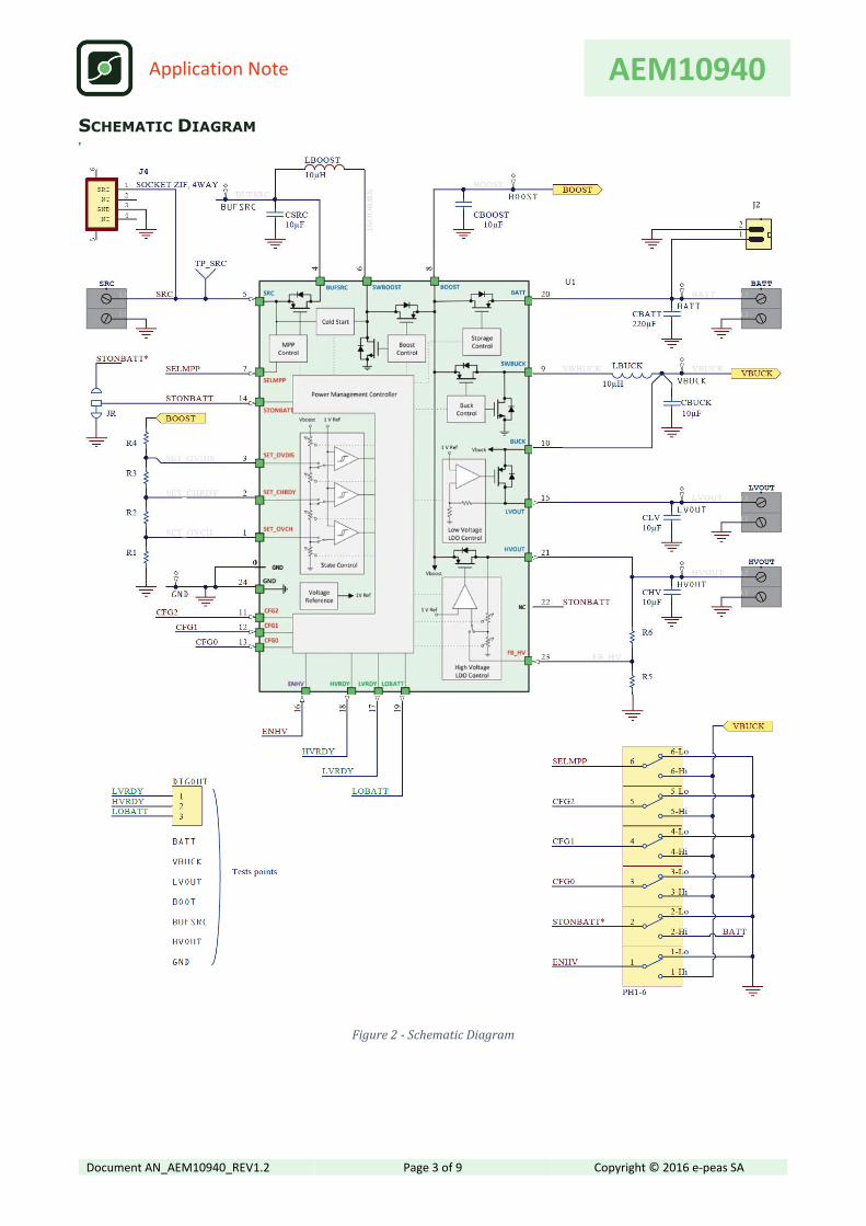
The PCB provides easy connections to the source of harvested energy, the storage element, the low voltage load and the high voltage load. It includes all the configuration items to set the device in any modes described in the data sheet. The control and status pins are available on standard pin headers, enabling wiring for any usage scenario and evaluation of the corresponding performance.
The AEM10940 Evaluation Board is your indispensable tool to take appropriate decisions (component selection, operating modes…) regarding the design of a highly efficient energy harvester subsystem in your target application.
FEATURES
Four two-way screw terminal blocks
- Source of energy (PV cell)
- Energy storage element (Li-Ion battery or super
capacitor)
- Low voltage load (typically a microcontroller)
- High voltage load (typically a radio transceiver)
This evaluation board is provided to you to assess the features and performances of the AEM10940 IC. This document explains how to make the board work for your use case and will guide you step by step to a successful experimentation.
Furthermore, e-peas engineers are available to assist you in case of question at [email protected].
Thank you for evaluating our groundbreaking AEM10940 IC. We are convinced it will answer your wireless sensor needs and open new application possibilities.
TABLE OF CONTENTS
Description ................................................................................................. 1 Features ....................................................................................................... 1 Appearance ................................................................................................ 1 Important note for the engineer ...................................................... 2 Table of Contents .................................................................................... 2
Storage Element ......................................................................... 5 Source Element .......................................................................... 5 Low Voltage Power Supply .................................................... 5 High Voltage Power Supply ................................................... 5 Control inputs ............................................................................. 5 Status Outputs ............................................................................ 5
Evaluating the Performance .............................................................. 6 Instrumenting the Storage Node ......................................... 6 Instrumenting the Source Node ........................................... 6 Instrumenting the Supply Nodes ......................................... 6 Warnings on Measurements ................................................. 6 Boost Converter Evaluation .................................................. 7 High Voltage Supply Evaluation........................................... 7 Low Voltage Supply Evaluation ........................................... 7 Quiescent Current Evaluation .............................................. 7
Engineering Information ..................................................................... 8 Part List ......................................................................................... 8 PCB information ........................................................................ 9
Use the screw terminal block J1 labeled BATT to connect the energy storage element. Take care of polarity: pin 2 receives positive voltage with respect to pin 1 (GND).
Alternatively, use the shrouded header connector J2, labeled BATT as well.
The storage element can be a battery, a high value capacitor or a super capacitor. It must be connected prior to the source element.
SOURCE ELEMENT
Use the screw terminal block J3 labeled SRC to connect the energy harvesting element. Take care of polarity: pin 2 receives positive voltage with respect to pin 1 (GND).
Alternatively, use the Molex connector J4, labeled SRC as well. GND is pin 3 and positive voltage is pin 1. The manufacturer reference is 52207-0460.
LOW VOLTAGE POWER SUPPLY
Use the screw terminal block J5 labeled LVOUT to connect the subsystem powered with the 1.8 V supply.
Take care of polarity: pin 2 provides positive voltage with respect to pin 1 (GND).
HIGH VOLTAGE POWER SUPPLY
Use the screw terminal block J6 labeled HVOUT to connect the subsystem powered with the 2.5 V to 3.3 V supply.
Take care of polarity: pin 2 provides positive voltage with respect to pin 1 (GND).
CONTROL INPUTS
One control input is available. Refer to the data sheet for full functionality. Consider in particular the paragraph “Power Gating”.
Input Pin Header name and label Pin
ENHV PH1 ENHV Pin 2 Central
Table 1 - Control Inputs
Use a jumper to wire the control input either to the Low side (permanent disable) or to High side (permanent enable).
Alternatively, attach a wire with a female pin connector to your system under evaluation to implement more complicated power gating schemes.
STATUS OUTPUTS
Three status outputs are available. Refer to the data sheet for full functionality.
Output Pin Header Pin number and label
LVRDY PH7 STATUS
Pin 1 LVRDY
HVRDY Pin 2 HVRDY
LOBATT Pin 3 LOBATT
Table 2 - Status Outputs
Attach a wire with a female pin connector to your system (e.g. a GPIO port), or use an oscilloscope probe.
CONFIGURATION
CONFIGURATION INPUTS
Four configuration inputs are available. Refer to the data sheet for full functionality. Consider in particular the paragraph “Built-in Configurations”.
Input Pin Header name and label Pin
SELMPP PH6 SELMPP
Pin 2 Central
CFG2 PH5 CFG2
CFG1 PH4 CFG1
CFG0 PH3 CFG0
Table 3 - Control Inputs
Use a jumper to wire the configuration input either to the Low side (LOW state) or to High side (HIGH state). Do not change the jumpers during operation.
CONFIGURATION RESISTORS
According to the data sheet under “Custom Configuration”, the user may have to solder six high-ohmic resistors (R1 to R6) to enable special modes of operation. The PCB provides footprints for through-hole resistors with a 7.68 mm pitch, which mates the common ¼ W axial lead package. Footprints for SMD 0805 resistors are also available.
With information provided in the data sheet, compute the required values according to the application.
Possible suppliers for suitable high-ohmic resistors are:
Manufacturer Series Ohmite HHV-25 Yageo MOX200
Table 4 - Resistors Manufacturers
RESTRICTIONS
Input Pin Header name and label
Jumper
STONBATT PH2 STONBATT Jumper on PCB bottom side
When using a battery, a special mode of operation involving STONBATT can be evaluated. Please contact e-peas for details.
Use a voltmeter and an ammeter according to one of the following methods to measure the electrical parameters at the storage element (Vbatt and Ibatt).
Method 1
Figure 5 - Storage Fixture 1
This method uses a real storage element.
Method 2
Figure 6 - Storage Fixture 2
This method emulates the storage element with an adjustable DC voltage source. Make sure the DC voltage source is able to sustain current peaks larger than 50 mA, notably if the voltage source features a current limiter. This is because Ibatt experiences current pulses from the part of the switching Boost and Buck converters.
For the same reason, the measurement of Ibatt should involve a time averaging computation to integrate the variations of current.
INSTRUMENTING THE SOURCE NODE
Use a voltmeter and an ammeter according to one of the following methods to measure the electrical parameters at the source element (Vsrc and Isrc).
As the Boost converter regulates the voltage at the SRC node, it is mandatory to emulate the energy harvester with a high impedance source.
Method 1
Figure 7 - Source Fixture 1
This method (recommended) uses an adjustable current source featuring a voltage limiter.
Set the voltage limit to the open circuit voltage of the emulated harvester (Voc). Voltage limitation occurs each time the MPP is evaluated (approximately every 15 sec).
Method 2
Figure 8 - Source Fixture 2
The second method uses an adjustable voltage source protected by a resistor Rsrc that emulates the internal impedance of the harvester.
Set the adjustable source to the open circuit voltage of the harvester (Voc).
The resistor value determines the power delivered by the source (Psrc) according to the following equations:
If SELMPP is HIGH If SELMPP is LOW
Rsrc =0.1875×Voc2
Peh Rsrc =
0.25×Voc2
Peh
Table 5 - Determining Rsrc
INSTRUMENTING THE SUPPLY NODES
Use a voltmeter and an ammeter according to one of the following methods to measure the electrical parameters at the system loads (Vlv, Ilv and Vhv, Ihv).
Method 1
Figure 9 - Supply Fixture 1
This method uses real system loads.
Method 2
Figure 10 - Supply Fixture 2
This method emulates a system load with a resistor.
Do not use a DC current source as a load, as this may result in negative voltage and damage the board if the IC enters its shutdown procedure.
WARNINGS ON MEASUREMENTS
Any item connected to the PCB (load, probe, storage device, etc.) involves a small current leakage that impacts negatively the measured performance figures. Whenever possible, disconnect unused items.
This is especially important for these measurements: - System quiescent current - Power conversion efficiency at low
output power
Ensure that the AEM10940 is in the normal operating mode regarding the charge management thresholds: - The overvoltage protection must not
be in action. - The voltage across the storage element
must be above the OverDischarge threshold
When evaluating output supplies, ensure that the relevant LDO is in operation as follows: - The relevant control input is High - After cold start, Vbatt has exceeded at
least once the ChargeReady threshold - Vbatt has not fallen below the
The Boost power conversion efficiency 𝜂𝐵𝑂𝑂𝑆𝑇 is the ratio of Pboost (power delivered by the boost converter) to Psrc (power supplied by the source element):
ηBOOST =Pboost
Psrc
Instrument the source node according to one of the described methods to evaluate Psrc:
Psrc = Vsrc×Isrc
Instrument the storage node supply according to one of the described methods to evaluate Pbatt:
Pbatt = Vbatt×Ibatt
Note that Ibatt flows into the storage element.
When Pbatt is larger than 1 mW, you can consider that Pboost amounts to Pbatt, the power supplied to the storage element.
At lower operating power, the board quiescent current Iq becomes relatively significant. Iq is also supplied by the Boost converter, but it is removed from the current delivered to the storage device. So, when Pbatt is smaller than 1 mW, a better evaluation of Pboost is:
The load connected to HVOUT is supplied by an LDO regulator.
The HV efficiency 𝜂𝐻𝑉 is the ratio of Phv (power delivered to the HV load) to Phvin (power supplied by the storage element to the LDO regulator):
ηHV =Phv
Phvin
Instrument the HVOUT supply according to one of the described methods, to evaluate Phv:
Phv = Vhv×Ihv
Instrument the storage node supply according to one of the described methods to evaluate Pbatt:
Pbatt = Vbatt×Ibatt
Note that Ibatt flows out of the storage element.
When Phv is larger than 1 mW, you can consider that Phvin amounts to Pbatt, the power delivered by the storage element.
At lower operating power, the board quiescent current Iq becomes relatively significant. Iq is absorbed from the BOOST node by the Buck converter. So, when Phv is smaller than 1 mW, a better evaluation of Phvin is:
The load connected to LVOUT is supplied by the Buck converter through an LDO regulator, which guarantees a high power conversion efficiency for any Vbatt voltage.
The LV efficiency 𝜂𝐿𝑉 is the ratio of Plv (power delivered to the LV load) to Pbatt (power supplied by the storage element to the Buck converter):
ηLV =Plv
Pbatt
This is the efficiency of the Buck converter combined with the low voltage LDO regulator. The board quiescent current contribution is included into this figure.
Instrument the LVOUT supply according to one of the described methods to evaluate Plv:
Plv = Vlv×Ilv
Instrument the storage node supply according to one of the described methods to evaluate Pbatt:
Connect a capacitor C of known value as the storage device. Keep in mind when selecting the capacitor that its leakage adds to Iq.
The instrument at the source node must deliver a power of at least 1 mW to speed up the charge of C.
Follow this procedure: - Let C charge until Vbatt reaches the OverCharge
threshold.
- Note the voltage across C as V1.
- Disconnect everything from the board, but the
capacitor C.
- Let Vbatt decay due to the quiescent current for a
known period of time T.
- Note the voltage across C as V2.
Do not leave the voltmeter connected during the decay period.
T should be chosen large enough to preserve accuracy and small enough to obtain a decay smaller than 200 mV.
Iq is obtained from:
𝐼𝑞 =𝐶×(𝑉1 − 𝑉2)
𝑇
Table 14 - Formula for Iq Evaluation
ENGINEERING INFORMATION The AEM10940 Evaluation Board can serve as a starting point for the electronic design of your own PCB.
To help you in this respect, this application note includes technical information that has been used to manufacture the Evaluation Board. Use this information as a source of inspiration for your specific project.
All files needed to reproduce the design with the schematic and layout tool suite Eagle are available on request from-e-peas.
PART LIST
This table includes a component order code as per the numbering system of the electronic distributor Farnell. This is for your convenience only.
Part Value Description Function Part Number Farnell Order Code C1 10 µF