Affordable Terahertz Components using 3D Printing
Amanpreet Kaur, Joshua C. Myers, Mohd Ifwat Mohd Ghazali, Jennifer Byford, and Premjeet Chahal
Department of Electrical and Computer Engineering, Michigan State University, East Lansing, MI- 48824, USA
[email protected]
Abstract
This paper presents the design and characterization of 3D
printed photonic crystal filter (quasi optic component) and
dielectric ridge waveguide (integrated component).
Commercially available 3D printer was used to print polymer
based components. Design and characterization of these
devices is carried out over a frequency range of 0.15 - 0.5
THz. The photonic crystal filter shows a stop band from 0.25 -
0.35 THz. Also a very narrow defect mode (notch filter) was
introduced by altering the structure of photonic crystal. The
dielectric ridge waveguide shows broadband THz propagation
characteristics. The transmission loss was determined to be
largely dominated by the loss characteristics of the polymer
material used.
Introduction
Over the last two decades, terahertz (THz) technologies have
attracted increased attention and interest due to its wide range
of applications such as spectroscopy, sensing, material
characterization, medical imaging, security, and
communication systems [1-3]. One of the major road blocks to
the adoption of THz technologies for consumer applications is
the cost of the system. Some of the key components such as
filters, waveguides, modulators, etc. that are readily available
in the RF and optical spectral region are missing from the THz
portfolio. THz components require further advancement with
respect to materials, fabrication and integration. For its
practical implementation, approaches to fabricate complex 3D
structures at low cost are necessary. Micromachining
techniques have been adapted to fabricate THz components.
However, micromachining techniques are expensive and
limited to fabrication on planar substrates. Thus, a simple
fabrication method is desirable that is low-cost and allows
fabrication of complex 3D structures. Recent developments in
rapid prototyping technologies may provide a path to meet this
challenge.
Rapid prototyping technologies such as stereo lithography,
fused deposition modeling, selective laser sintering, polymer-
jetting have been explored for fabricating microwave circuits
[4, 5]. Among these, polymer stereolithography and polymer-
jetting are fast, and additive printing (3D printing) processes
capable of building high aspect-ratio micro structures with
high resolution. The 3-D parts are made by curing liquid
polymer using a laser beam in a layer by layer process.
Through layering of fine structures and by using temporary
support structures complex 3D parts can readily be made.
Advantages of 3D printing include design flexibility, short
cycle time, good reproducibility, vast choice of materials and
overall low cost. Passive THz components such as filters,
waveguides, antennas and couplers are the building blocks of
a THz system and hence fabrication of these using 3D printing
is of great interest. While 3D printing has been used
extensively to print large objects, the use of 3D printing for
THz devices has not been well studied, although a few
examples have been demonstrated recently[6-8].
One of the key components required for THz circuits are
tunable/ reconfigurable quasi-optical THz devices that can
control the spatial transmission of THz signal. Also, the ability
to manipulate the THz signal using structures like photonic
crystals (PC) is of great interest for application in
communication and sensing. The PC with distorted periodicity
are also of significant interest due to their highly localized
defect mode. This property can be used for design of filter
with very narrow transmission band (notch filter), resonant
cavities, and waveguides [9].
Along with quasi-optical THz system components, wafer
level integration is desirable to further reduce the cost of THz
systems. There are several challenges to realizing THz
integrated circuits such as design, microfabrication, and lack
of compatible materials. THz waveguide is one of the
important components needed to achieve integrated circuits.
Various types of THz waveguides such as metallic waveguide,
Plasmonic waveguide, hollow-core photonic crystal fibers,
and dielectric waveguides etc. have been studied in past [10,
11]. However, these structures are difficult to fabricate at the
wafer level due complexity of the manufacturing process.
Planar dielectric waveguides such as ribbon waveguides and
Dielectric Ridge waveguide (DRW) can be used for the
realization of a low cost THz waveguide with component
integration.
Recently, Pandey et. al. showed the use of 3D printing for
fabrication of spoof plasmonic waveguide where the structure
is first printed with polymer resin and then blanket coated with
metal film [7]. In these waveguides the wave propagates on
the surface, i.e. at the metal-air interface. These waveguides
are narrowband and thus limited in application. Dielectric
waveguides such as ribbon waveguide carries THz signal
efficiently as the signal travels at the air dielectric interface
and have wide band operation [12]. However, they require
thin films of high dielectric constant material. Ridge
waveguide is another good candidate as a low-loss THz
waveguide, whereas here the signal travels in the bulk of the
dielectric material and can be designed using low dielectric
constant materials. Similar to the ribbon waveguide, it does
not require sub-wavelength size dimensions. So, it is possible
to realize such a structure using 3D printing.
This paper demonstrates the use of conventional 3D
printing to fabricate two types of circuits: quasioptical and
integrated. A photonic crystal based quasioptical filter, and an
integrated DRW and power splitter are demonstrated. Such
functional THz devices are needed in THz sensing, imaging
and communications. These structures require feature sizes on
the scale of the wavelength or below. For our frequency range
978-1-4799-8609-5/15/$31.00 ©2015 IEEE 2071 2015 Electronic Components & Technology Conference
of interest (0.1 – 1 THz), the corresponding wavelength range
is 3 – 0.3 mm in free space. Thus, the printing resolution of
existing 3D printed system is well suited for fabrication of
components for the terahertz range.
These components are printed using a professional-grade
commercially available 3D printer (Objet Connex350) using a
photo-polymer resin. All the THz components measured here
are fabricated using 3D printed material called “verowhite”
which has a dielectric constant εr ~ 2.8 at the frequency of
interest and a loss tangent, tanδ, of ~0.04. The simulation and
experimental results for 3D printed structures are presented in
the next section. THz frequency domain spectroscopy (THz-
FDS) is used here to characterize the transmission properties
of the components.
Quasi-Optic components: Filters
This paper demonstrates THz band stop filter based on 1-
D photonic crystal (PC) design. The PC’s are artificially
periodic structures composed of two or more mediums with
different permittivity. In 1D PCs, the periodic change of the
permittivity occurs only in one direction. They have the
advantage of simple structure and thus can be easily
fabricated. The parameters that play an important role in
achieving good performance are the thickness of each of the
dielectric layers and the total number of layers. In order to
work as a THz filter the PC structure should be composed of
stack of quarter wavelength thick high and low permittivity
material layers.
PC’s with defect in its lattice is also of great interest for
many applications such as sensing, wave guiding, notch filter.
A defect can be created in a 1D PCs, by using one of the
layers to have a slightly different dielectric constant or
thickness than the other layers. A defect was created here by
replacing the center high permittivity dielectric layer with air.
The Photonic crystal filter is modeled here using a commercial
finite element EM solver, HFSS. The filter was designed to
operate in the lower THz range (~ 0.3 THz). The PCF is
composed of 10 layers of 0.150 mm thick 3D printed material
(εr = 2.8 at 0.3 THz) separated from each other by air gap of
0.25 mm thickness. Figure 1 shows the simulated transmitted
signal (S21) of the filter over a frequency range of 0.3 - 0.5
THz.
The filter has a stop band over a frequency range of 0.25 -
0.35 THz. For the filter with a defect layer, the stop band is
comparatively narrow and slightly shifted towards higher
frequency. It also shows a single defect mode near 0.27 THz,
within the stop band region which is centered at 0.3 THz.
These highly localized modes are useful for applications such
as sensing, narrow band pass filters, antenna designs, noise
suppression, etc. The filter was modeled for two different
values of dielectric loss tangent (tan δ) of 0.01 and 0.05. As
expected, the transmitted signal for filter designed with lower
loss dielectric is higher. Thus, dielectric materials with lower
loss are desired for low transmission losses. The individual
layers of the periodic structure were fabricated using a 3D
printer. These structures were stacked together to form a 1D
PC as shown in Figure 2. The 3D material acts as a high
dielectric layer and the spacer at the edges of the dielectric
slab creates air gap between subsequent slabs (Figure 2(a)).
The thickness of air-spacer is 0.25 mm while the dielectric
layer is 0.15 mm thick. The stack consists of total of 10 layers.
Figure 2(b) shows the schematic and optical micrograph of PC
stack.
Figure 1: Simulated S21 of 1D photonic crystal filter with and
without a defect layer with different dielectric loss tangent (tan
δ=0.01, and 0.05).
Figure 2: Photonic crystal based filter (a) Schematic of single
layer and the stack (b) Optical picture of 3D printed layer and
stack.
To introduce a defect, a window was opened in the lattice
by removing one dielectric layer and replaced with air
dielectric. The transmission spectra of 3D printed filters were
measured using a frequency-domain THz measurement setup,
Emcore PB-7200. In this system, the THz signal is generated
by mixing narrow band wavelengths from two different lasers
using a low-temperature GaAs film coupled to an antenna.
The signal is detected using a laser based heterodyne mixer.
The collimated THz beam from the transmitter (Tx)
propagates through air and is detected on the other end using a
heterodyne mixer. The samples are placed in between the
transmitter and the receiver (Rx) heads for transmission
measurements. The filters measured in here were directly
placed in the THz beam path and the amplitude of the
transmitted signal was measured.
For the measurement of the filters, first a background
signal was measured by removing the sample from the THz
beam path. This signal was used as the reference. The
measured transmitted signal through the filter with and
without defect is shown in Figure 3. The measured result
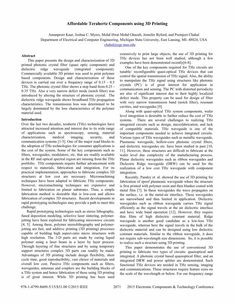
2072
matches closely with simulation results with similar stop band
and defect mode. These results show that 3D printing can be
easily used for making good quality THz filter. The filters can
be further improved by using polymer materials with lower
dielectric losses as opposed to “Verowhite” material used
here.
Figure 3: Experimental results for Photonic crystal based
filter with and without defect.
Integrated Circuits Components:
Ridge Waveguides (RWG)
There is growing interest in THz integrated circuits to
realize similar circuits as monolithic microwave integrated
circuits (MMICs). Some of the challenges to achieving THz
integrated circuits are design and microfabrication
complexities, and lack of availability of low loss materials.
THz waveguides is one of the important components that form
a basic building block for integrated circuits. Conventional
metal based transmission lines like microstrips have high
losses. Dielectric based waveguides are attractive as they
provide low loss propagation of THz signals. There is need of
simple prototyping process like 3D printing for realization of
dielectric waveguides and associated components. In this
paper, the proposed ridge waveguide were fabricated using a
simple and low cost 3D printed technology. Also, the
applicability of these waveguides in a power splitter is
demonstrated.
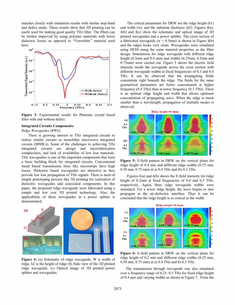
Figure 4: (a) Schematic of ridge waveguide, W is width of
ridge, h2 is the height of ridge (b) Side view of the 3D printed
ridge waveguide. (c) Optical image of 3D printed power
splitter and waveguides.
The critical parameters for DRW are the ridge height (h1)
and width (w), and the substrate thickness (h2). Figures 4(a),
4(b) and 4(c) show the schematic and optical image of 3D
printed waveguides and a power splitter. The cross section of
a fabricated waveguide (w = 0.5mm) is shown in Figure 4(b)
and the edges looks very clean. Waveguides were simulated
using HFSS using the same material properties as the filter
design. Simulations for ridge waveguide with different ridge
height (0.2mm and 0.4 mm) and widths (0.25mm, 0.5mm and
0.75mm) were carried out. Figure 5 shows the electric field
intensity inside the waveguide across the cross section with
different waveguide widths at fixed frequencies of 0.3 and 0.4
THz. It can be observed that the propagating fields
concentrate right beneath the ridge. The fields for the same
geometrical parameters are better concentrated at higher
frequency (0.4 THz) than at lower frequency (0.3 THz). There
is an optimal ridge height and width that allows optimum
concentration of propagating wave. When the ridge is much
smaller than a wavelength, propagation of multiple modes is
observed.
Figure 5: E-field pattern in DRW on the vertical plane for
ridge height of 0.4 mm and different ridge widths (0.25 mm,
0.50 mm, 0.75 mm) at a) 0.4 THz and (b) 0.3 THz.
Figures 6(a) and 6(b) shows the E-field intensity for ridge
height of 0.2mm at fixed frequencies of 0.4 and 0.3 THz,
respectively. Again, three ridge waveguide widths were
simulated. For a lower ridge height, the wave begins to also
propagate at the air-dielectric interface. Thus it can be
concluded that the ridge height is as critical as the width.
Figure 6: E-field pattern in DRW on the vertical plane for
ridge height of 0.2 mm and different ridge widths (0.25 mm,
0.50 mm, 0.75 mm) at a) 0.4 THz and b) 0.3 THz.
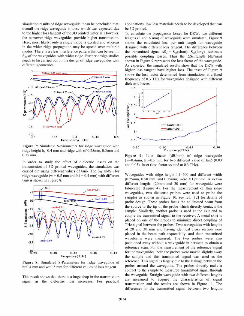
The transmission through waveguide was also simulated
over a frequency range of 0.25- 0.5 THz for fixed ridge height
of 0.4 mm and varying widths as shown in Figure 7. From the
2073
simulation results of ridge waveguide it can be concluded that,
overall the ridge waveguide is lossy which was expected due
to the higher loss tangent of the 3D printed material. However,
the narrower ridge waveguides provide higher transmission.
Here, most likely, only a single mode is excited and whereas
in the wider ridge propagation may be spread over multiple
modes. There is a clear interference pattern that can be seen in
S21 of the waveguides with wider ridge. Further design studies
needs to be carried out on the design of ridge waveguides with
different geometries.
Figure 7: Simulated S-parameters for ridge waveguide with
ridge height h1=0.4 mm and ridge with of 0.25mm, 0.5mm and
0.75 mm.
In order to study the effect of dielectric losses on the
transmission of 3D printed waveguides, the simulation was
carried out using different values of tanδ. The S21 andS11 for
ridge waveguide (w = 0.5 mm and h1 = 0.4 mm) with different
tanδ is shown in Figure 8.
Figure 8: Simulated S-Parameters for ridge waveguide of
h=0.4 mm and w=0.5 mm for different values of loss tangent.
This result shows that there is a huge drop in the transmission
signal as the dielectric loss increases. For practical
applications, low loss materials needs to be developed that can
be 3D printed.
To calculate the propagation losses for DRW, two different
lengths (3 and 6 mm) of waveguide were simulated. Figure 9
shows the calculated loss per unit length for waveguide
designed with different loss tangent. The difference between
the transmitted signal ΔS21= S21(short)- S21(long) subtracts
possible coupling losses. Thus the ΔS21/length (dB/mm)
shown in Figure 9 represents the loss factor of the waveguide.
As expected, the simulated results show that the DRW with
higher loss tangent have higher loss. The inset of Figure 9
shows the loss factor determined from simulations at a fixed
frequency of 0.3 THz for waveguides designed with different
dielectric losses.
Figure 9: Loss factor (dB/mm) of ridge waveguide
(w=0.4mm, h1=0.5 mm for two different value of tanδ (0.03
and 0.05). Inset (loss factor vs tanδ at 0.3 THz).
Waveguides with ridge height h1=400 and different width
(0.25mm, 0.50 mm, and 0.75mm) were 3D printed. Also two
different lengths (20mm and 30 mm) for waveguide were
fabricated (Figure 4). For the measurement of thin ridge
waveguides, two dielectric probes were used to probe the
samples as shown in Figure 10, see ref. [12] for details of
probe design. These probes focus the collimated beam from
the source to the tip of the probe which directly contacts the
sample. Similarly, another probe is used at the exit end to
couple the transmitted signal to the receiver. A metal skirt is
placed on one of the probes to minimize direct coupling of
THz signal between the probes. Two waveguides with lengths
of 20 and 30 mm and having identical cross section were
placed in the beam path sequentially, and their transmitted
waveforms were measured. The two probes were also
positioned away without a waveguide in between to obtain a
reference scan. For the measurement of the reference signal
for the waveguides, both the probes were moved slightly away
the sample and this transmitted signal was used as the
reference. This signal is largely due to the leakage between the
probes around the waveguide. The probes directly make a
contact to the sample to measured transmitted signal through
the waveguide. Straight waveguide with two different lengths
are measured to acquire the characteristics of signal
transmission and the results are shown in Figure 11. The
differences in the transmitted signal between two lengths
2074
indicate the effective transmission loss associated with the
difference in the waveguide lengths.
Figure 10: THz measurement set-up for measuring ridge
waveguide.
This loss is largely due to the high loss of the dielectric
material used here. The transmitted signals decay at higher
frequencies which can be contributed to loss occurring due to
dielectric probes which are not optimized for wide frequency
bandwidth operation. Also, the signal from the THz source
decreases with increase in frequency. At higher frequencies (>
0.35 THz) the difference in transmitted signal decreases. This
is an artifact from the poor signal to noise ratio achieved at
low transmitted signals.
Figure 11: Measured Transmission signal intensity of DRW
with two different lengths, short (20 mm) and long (30 mm)
with fixed width and height of 0.25mm and 0.4 mm,
respectively.
Waveguides with fixed height of 0.4 mm and length of
20mm, and different ridge widths (0.25 mm, 0.50 mm, 0.75
mm) were also measured and the results are shown in Figure
12. All of the waveguides having different widths show good
transmission properties and their transmission characteristics
looks similar. Overall, these results indicated that 3D printing
can be used to print THz waveguides. Loss can be decreased
with further improvement in material properties and reduced
surface roughness.
Figure 12: Measured Transmission Intensity for waveguides
with different ridge width (0.25mm, 0.5 mm, 0.75 mm).
Power Splitter
To demonstrate a functional THz circuit, a 1:2 RWG based
power splitter was designed and 3D printed as shown in
Figure 4. The splitter consists of 15 mm input arm and two 15
mm output arms, with ridge height of 04 mm and ridge width
of 0.5 mm. The measured transmission signal intensity was
measured for both arms over a frequency range of 0.15 THz to
0.5 THz. The measured result for power splitter is shown in
Figure 13. The transmitted signal from both arms is
approximately equal as expected from a 1:2 power splitter.
Figure 13. Measured transmitted signal intensity for RWG
based power splitter.
These results indicate that 3-D printed waveguide can
serve as a critical building block for THz integrated circuits.
This process is wafer level compatible and can be carried out
at room temperature. Thus, it is compatible with a host of low
cost large area substrates. 3D printing can be adopted for post
2075
processing of passive structures on semiconductor wafers.
Also, with further development, passive elements that require
combination of metal and dielectric layers can be directly
printed at the wafer level.
Conclusion
This paper experimentally demonstrated that conventional 3D
printing is well suited for fabrication of THz passive
components such as straight ridge waveguides, splitters and
filters. Quasi-optical PC based THz filters were fabricated by
polymer jetting UV resin. Results of the transmission loss
showed good agreement with simulations. Wide band dielctric
ridge waveguides were also designed and 3D printed. A 1:2
power splitter wide band frequency operation was also
demonstrated using this technique having. The higher loss in
the transmitted signal in the 3D printed structures can be
attributed to surface roughness (~10 m) that results from the
printing process and the high loss of the dielectric material.
With further improvements in printing resolution and low loss
materials, this technique will be useful in printing of THz
large area low cost passive components. Also, it can be
adopted to directly print passive components on a
semiconductor wafer for the manufacture of THz integrated
circuits.
Acknowledgments
The authors would like to thank the members of Terahertz
Systems Lab (TeSLa) and Brian Wright for their help.
References
1. M. Tonouchi, "Cutting-edge terahertz technology," Nature
photonics, vol. 1, pp. 97-105, 2007.
2. K. Humphreys, J. Loughran, M. Gradziel, W. Lanigan, T.
Ward, J. Murphy, et al., "Medical applications of terahertz
imaging: a review of current technology and potential
applications in biomedical engineering," in Engineering in
Medicine and Biology Society, 2004. IEMBS'04. 26th
Annual International Conference of the IEEE, 2004, pp.
1302-1305.
3. D. M. Mittleman, R. H. Jacobsen, R. Neelamani, R. G.
Baraniuk, and M. C. Nuss, "Gas sensing using terahertz
time-domain spectroscopy," Applied Physics B: Lasers
and Optics, vol. 67, pp. 379-390, 1998.
4. B. Liu, X. Gong, and W. J. Chappell, "Applications of
layer-by-layer polymer stereolithography for three-
dimensional high-frequency components," Microwave
Theory and Techniques, IEEE Transactions on, vol. 52,
pp. 2567-2575, 2004.
5. K. F. Brakora, J. Halloran, and K. Sarabandi, "Design of
3-D monolithic MMW antennas using ceramic
stereolithography," Antennas and Propagation, IEEE
Transactions on, vol. 55, pp. 790-797, 2007.
6. Z. Wu, J. Kinast, M. Gehm, and H. Xin, "Rapid and
inexpensive fabrication of terahertz electromagnetic
bandgap structures," Optics Express, vol. 16, pp. 16442-
16451, 2008.
7. S. Pandey, B. Gupta, and A. Nahata, "Terahertz plasmonic
waveguides created via 3D printing," Optics Express, vol.
21, pp. 24422-24430, 2013.
8. K. Y. Park, N. Wiwatcharagoses, and P. Chahal, "Wafer-
level integration of micro-lens for THz focal plane array
application," in Electronic Components and Technology
Conference (ECTC), 2013 IEEE 63rd, 2013, pp. 1912-
1919.
9. H. Nemec, P. Kuzel, L. Duvillaret, A. Pashkin, M.
Dressel, and M. Sebastian, "Highly tunable photonic
crystal filter for the terahertz range," Optics Letters, vol.
30, pp. 549-551, 2005.
10. C. D. Nordquist, M. C. Wanke, A. M. Rowen, C. L.
Arrington, M. Lee, and A. D. Grine, "Design, fabrication,
and characterization of metal micromachined rectangular
waveguides at 3 THz," in Antennas and Propagation
Society International Symposium, 2008. AP-S 2008. IEEE,
2008, pp. 1-4.
11. L.-J. Chen, H.-W. Chen, T.-F. Kao, J.-Y. Lu, and C.-K.
Sun, "Low-loss subwavelength plastic fiber for terahertz
waveguiding," Optics Letters, vol. 31, pp. 308-310, 2006.
12. X. Yang and P. Chahal, “On-wafer terahertz ribbon
waveguides using polymer ceramic nanocomposites,"
Components, Packaging and Manufacturing Technology,
IEEE Transactions on, vol. 5, pp. 245-255, Feb 2015.
13. J. A. Hejase, B. Schulte, and P. Chahal, "Design and test of
wide-band terahertz dielectric sub-wavelength focusing
probes," in Electronic Components and Technology
Conference (ECTC), 2011 IEEE 61st, 2011, pp. 1035-
1040.
2076