AFRL-OSR-VA-TR-2015-0050 ADVANCED RF SOURCES BASED ON NOVEL NONLINEAR TRANSMISSION LINES Y. Lau UNIVERSITY OF MICHIGAN Final Report 01/29/2015 DISTRIBUTION A: Distribution approved for public release. AF Office Of Scientific Research (AFOSR)/ RTB Arlington, Virginia 22203 Air Force Research Laboratory Air Force Materiel Command
Transcript
AFRL-OSR-VA-TR-2015-0050
ADVANCED RF SOURCES BASED ON NOVEL NONLINEAR TRANSMISSION LINES
Y. LauUNIVERSITY OF MICHIGAN
Final Report01/29/2015
DISTRIBUTION A: Distribution approved for public release.
AF Office Of Scientific Research (AFOSR)/ RTBArlington, Virginia 22203
Air Force Research Laboratory
Air Force Materiel Command
REPORT DOCUMENTATION PAGE Form Approved
OMB No. 0704-0188 Public reporting burden for this collection of information is estimated to average 1 hour per response, including the time for reviewing instructions, searching existing data sources, gathering and maintaining the data needed, and completing and reviewing this collection of information. Send comments regarding this burden estimate or any other aspect of this collection of information, including suggestions for reducing this burden to Department of Defense, Washington Headquarters Services, Directorate for Information Operations and Reports (0704-0188), 1215 Jefferson Davis Highway, Suite 1204, Arlington, VA 22202-4302. Respondents should be aware that notwithstanding any other provision of law, no person shall be subject to any penalty for failing to comply with a collection of information if it does not display a currently valid OMB control number. PLEASE DO NOT RETURN YOUR FORM TO THE ABOVE ADDRESS. 1. REPORT DATE (DD-MM-YYYY)
2. REPORT TYPE
3. DATES COVERED (From - To)
4. TITLE AND SUBTITLE
5a. CONTRACT NUMBER
5b. GRANT NUMBER
5c. PROGRAM ELEMENT NUMBER
6. AUTHOR(S)
5d. PROJECT NUMBER
5e. TASK NUMBER
5f. WORK UNIT NUMBER
7. PERFORMING ORGANIZATION NAME(S) AND ADDRESS(ES)
8. PERFORMING ORGANIZATION REPORT NUMBER
9. SPONSORING / MONITORING AGENCY NAME(S) AND ADDRESS(ES) 10. SPONSOR/MONITOR’S ACRONYM(S) 11. SPONSOR/MONITOR’S REPORT NUMBER(S) 12. DISTRIBUTION / AVAILABILITY STATEMENT
13. SUPPLEMENTARY NOTES
14. ABSTRACT
15. SUBJECT TERMS
16. SECURITY CLASSIFICATION OF:
17. LIMITATION OF ABSTRACT
18. NUMBER OF PAGES
19a. NAME OF RESPONSIBLE PERSON
a. REPORT
b. ABSTRACT
c. THIS PAGE
19b. TELEPHONE NUMBER (include area code)
Standard Form 298 (Re . 8-98) vPrescribed by ANSI Std. Z39.18
26-01-2015 Final report 09/01/2009-10/31/2014
Advanced RF sources based on novel nonlinear transmission lines FA9550-09-1-0662
Yue-Ying Lau
University of Michigan Department of Nuclear Engineering and Radiological Sciences 2355 Bonisteel Blvd Ann Arbor, MI 48109-2104
Dr. Jason Marshall Air Force Office of Scientific Research 875 N. Randolph St Arlington, VA 22203
AFOSR/RTB
DISTRIBUTION A
We compute the Green’s function on a slow wave structure. We derive the scaling laws for the contact resistance of both bulk contact and thin film contact, with general aspect ratios and vastly different resistivity in the different contact members. We discover a voltage scale, which depends only on material property, that characterizes the robustness of the material against runaway heating due to electro-thermal instability. We identify the role of the RF magnetic field, and the role of RF electric field, in the enhanced heating of rough surfaces including bumps and troughs. We investigate the effects of surface irregularities, and more generally of random manufacturing errors, on the performance of traveling wave amplifiers. We construct a scaling law for the limiting current for spherical and cylindrical diode, which is the first successful attempt in 90 years to provide a simple analytic scaling for the celebrated (numerical) solutions of Langmuir and Blodgett. We derive a new scaling law for a ballistic diode, which is a key component for the “vacuum transistor”, a high-speed transistor envisioned for the future.
High power mirowave sources, electrical contact, surface heating
U U U
23Y. Y. Lau
734-764-5122
Final Report
“Advanced RF Sources Based on Novel Nonlinear Transmission Lines”
We have studied a variety of fundamental problems that are important to advanced RF sources based on nonlinear transmission lines (NLTL’s). We computed the Green’s function on a slow wave structure. This is a prerequisite for the generation of high power microwave from the output voltage pulse of a nonlinear transmission line. Many complimentary issues were studied, such as electrical contacts and the effects of rough surfaces on the heating and on the performances of the device. Their technological significance crosses many disciplines, and several existing and potential future collaborations with other institutions resulted from this research. The major novel results are summarized below. 1.We formulated the Green’s function in terms of the eigenmodes for a general slow wave structure. It is validated by a simulation code in a specific example. [1] 2. We provided scaling laws for vertical thin film contacts [4,6], and showed that edge heating is not serious in the thin film limit [7]. 3. We provided scaling laws for horizontal thin film contacts [6,10,11,15], including a 3-terminal device [12], and showed that edge heating is very serious in the thin film limit [11,14]. We also found a voltage scale, which depends only on materials property [13], that characterizes the robustness of the material against runaway heating due to electro-thermal instability. 4. We constructed a scaling law for the limiting current for spherical and cylindrical diode [18]. It is the first successful attempt in 90 years to provide a simple analytic scaling for the numerically-tabulated solutions of Langmuir and Blodgett, which are still in use today. 5. We derived a new scaling law for a ballistic diode [21], which is a key component for the “vacuum transistor”, a high-speed transistor envisioned for the future. 6. We identified the role of the RF magnetic field, and the role of RF electric field, in the enhanced heating of rough surfaces including bumps and troughs [24], at the same time we validated a powerful numerical code that was developed elsewhere. 7. We investigated the effects of surface irregularities, and more generally of random manufacturing errors, on the performance of traveling wave amplifiers. [26,27,28] Collaborations were held with the Air Force Research Laboratory (Kirtland) [1], Naval Research Laboratory [27], Caltech [24], Singapore [18], and industry [11,14]. Colleagues from the Air Force Institute of Technology, AFRL (Wright Patterson), UC San Diego, U of Maryland, and MIT, recently expressed an interest in our works, either using it or in collaborating with us.
3
2.0 Research Topics
2.1 Nonlinear Transmission Line (NLTL)
High power RF radiation sources typically require an electron beam. There are substantial advantages if the radiation can be generated without using an electron beam, such as by using a nonlinear transmission line (NLTL) to transform an input pulse into high frequency components. The key question on this type of beam-free radiation source is the conversion of the NLTL’s output voltage pulses into radiation. The AC voltage pulse excitation coupled to the slow wave structure (SWS) would generate an electromagnetic wave or set of waves on the circuit, which could then be coupled out as radiation. For a general temporal excitation, the Green’s function for the SWS is of fundamental interest.
We have constructed the Green’s function for the SWS to show how the SWS would respond to an impulse excitation [1]. The Green’s function includes all radial modes, and for each radial mode, all space harmonics. We compare the analytic solution of the frequency response on the SWS with that obtained from a particle-in-cell code, as shown in Fig. 1. Favorable comparison is obtained when the first few lower order modes are resonantly excited. This gives confidence in the prediction of converting a pulse train into radiation using a slow wave structure.
a) b)
Fig. 1. Frequency response of the SWS, obtained from a), analytical theory, and b), particle-in-cell simulation using ICEPIC [1].
4
2.2 Bulk contact
Because of the surface roughness on a microscopic scale, true contact between two pieces of conductors occurs only at the asperities (small protrusions) of two contacting surfaces. Current flows only through these asperities, leading to contact resistance. Electrical contact is a very important issue to high power microwave (HPM) sources. It is also critical to thin film devices and integrated circuits, carbon nanotube based cathodes and interconnects, field emitters, and wire-array z-pinches, etc. Contact problems account for about 40% of all electrical/electronic failures [2]. We therefore spent very significant efforts in the evaluation of contact resistance.
For decades, the fundamental model of electrical contact remains that of Holm [3], which is based on simplified assumptions. We have substantially generalized Holm’s a-spot model to higher dimensions, including vastly different materials at the joints, in an attempt to quantify the effects of contaminants on electrical contacts [4, 5, 6, 7]. Simple and explicit scaling laws for the electrical contact resistance with dissimilar materials are constructed. Sample calculations are shown in Fig. 2. The model assumes arbitrary resistivity ratios and aspect ratios in the current channels and their contact region, for both Cartesian and cylindrical geometries [4]. The scaling laws have been favorably tested in several limits, and in sample calculations using a numerical simulation code.
If the length of the conducting channel in Fig. 2 (a) is small compared to its transverse dimension, the model is extended to study vertical thin film contact [7], as shown in Fig. 3(a). Figure 3(b) shows the general scaling laws for the constriction resistance with arbitrary resistivity ratios and geometric aspect ratios. In the limit of small film thickness, we found that current crowding in the vertical contact is far less serious than the current crowding in the horizontal contact (Section 2.3 below).
5
(a) (b)
(c) (d)
Fig. 2. (a) Generalized a-spot contact, in either Cartesian or cylindrical geometries. Holm’s a-spot corresponds to the cylindrical geometry with h = 0, a << b, a << c, (b) and (c) normalized contact resistance as a function of b/a, and ρ1/ρ2, respectively, for cylindrical geometry, (d) total resistance of a cylindrical channel calculated from analytic theory (solid lines) in excellent agreement with that from simulation (symbols).
(a) (b)
6
Fig. 3. (a) Vertical thin film contact, (b) normalized contact resistance as a function of the aspect ratio a/h2 in (a), with ρ1/ρ2 = 100, 1, and 0.01 (top to bottom). [7]
2.3 Thin film horizontal contact
There is another class of thin film contacts where the current flow in the base is in the horizontal direction, parallel to the base (as shown in Figs. 4b and 4c), instead of vertical to the base (as shown in Fig. 3a). Thin-film contacts of this sort are also ubiquitous to modern electronic devices. Once more, contact resistance is a fundamental limiting factor to their electronics performance, especially for novel materials with extremely high conductivity used to build conducting channels. How to accurately characterize contact resistance is an important issue.
We have developed extensive models for thin film contact, including the effects of dissimilar materials [8-15] for both Cartesian and cylindrical geometries. For the Cartesian geometry, we have extended the model to study a general 3-terminal structure [12], where the voltages at the three terminals may take arbitrary values, as shown in Fig. 4a. We solved the potential and current flows for such a general structure by decomposing it into an even solution (Fig. 4b) and an odd solution (Fig. 4c). The normalized contact resistance for both cases is shown in Fig. 5. It is found that the contact resistance is insensitive to the resistivity ratio for a/h2 < 1, but is rather sensitive to the resistivity ratio for a/h2 > 1 where a is the constriction size and h2 is film thickness. Typically, the minimum contact resistance in the even solution is realized with a/h ~ 1, [8] for both Cartesian and cylindrical cases, as shown in Fig. 5a. The current crowding and current partition are examined thoroughly. It is found that the hottest spot, i.e. the location of the strongest current crowding and therefore highest temperature due to joule heating, occurs at the constriction corner near the source side, which is point B in Fig. 4(c).
(a) (b) (c)
Fig. 4. (a) 3-terminal Cartesian thin film contact structure of dissimilar materials, with arbitrary terminal voltage at the three terminals, which may be considered as a superposition of an even solution (b) and an odd solution (c). [12]
7
(a)
(b)
Fig. 5. Normalized contact resistance for (a) the even solution, and (b) the odd solution of thin film contact in Figs. 4b and 4c, respectively. [12]
We discovered an intrinsic voltage scale that governs the electro-thermal instability in semiconductors [13]. The voltage Vs is deduced from the heat conduction equation as,
,
where κ is the thermal conductivity and σ0’ is the rate of change of the electrical conductivity with respect to temperature. It is clear that Vs depends only on material properties and is independent of geometry and the operating voltage. Vs measures the intrinsic tolerance of the material to electro-thermal instability. Numerical values of Vs are consistent with the well-known
8
properties of several common materials [13]. For example, the value of Vs for SiC is 2 orders of magnitude higher than that of Ge, Si and C, implying that SiC is among the most robust semiconductor against thermal runaway (a well-known fact).
Most recently, we extended our thin film contact model to include a resistive interface layer [15], which represents a typical metal-semiconductor contact, as shown in Fig. 6a. We developed an exact field solution for the contact in Fig. 6a, accounting fully the spreading resistance caused by the fringe fields near the constriction corner, which are generally ignored in the typical transmission line model (TLM) in Fig. 6b. Our model is compared with TLM, shown in Fig. 7a. When the interface resistance rc is small, TLM becomes inaccurate. Figure 7b shows the regime when the total contact resistance is dominated by the interface resistance ( <0.5) or by the spreading resistance ( > 0.5) due to current crowding.
Fig. 6. (a) Electrical contact including specific interfacial resistivity ρc, and (b) its transmission line model (TLM). In (a), an infinitesimally thin resistive interface layer is sandwiched between Regions I and II. [15]
9
(a)
(b)
Fig. 7. (a), Comparison of normalized contact resistance from our exact field solution (solid line) and TLM (dashed line). (b) Contour plot of , which is the ratio of spreading resistance over the total contact resistance. Symbols represent experimental data in the literature. [15]
Issues on the measurement of contact resistance and spreading resistance are studied in Ref. [14]. The thin film contact models are also extended to a contact of arbitrary shape, and to high frequency AC conduction in a constricted bulk solid [6, 14].
10
2.4 Classical and ballistic diode
(a) Classical diode
For 90 years, there has been no scaling law for the maximum current (also known as the limiting current) in cylindrical and spherical diodes. The limiting current density is only numerically tabulated in the celebrated papers by Langmuir and Blodgett (L-B) [16, 17]. We recently found a novel new scaling for the L-B law for both cylindrical and spherical diodes, which is expressed as [18]
,
where Ec is the surface electric field on the cathode of the vacuum diode. This dependence is valid whether Ra/Rc is greater than or less than unity, where Ra and Rc are respectively the anode and cathode radius. F is the correction factor, for a cylindrical diode is given by [18]
,
and for a spherical diode by [18],
,
where s = ln[ln(1+Rc/Ra)] and s0 = ln[ln(2)]. The above scalings are accurate to within 5% for the entire practical range 3×10⁻⁵ < Rc/Ra < 500 that was considered by Langmuir and Blodgett [16,17], as shown in Fig. 8.
(a) (b) Fig. 8. Comparison of the new scaling Japp with the Langmuir-Blodgett law, for (a) cylindrical diode, (b) spherical diode. In the calculation, the inner radius either Ra or Rc is 1 cm, the applied voltage is Vg = 1 V. [18]
11
(b) Ballisitic diode
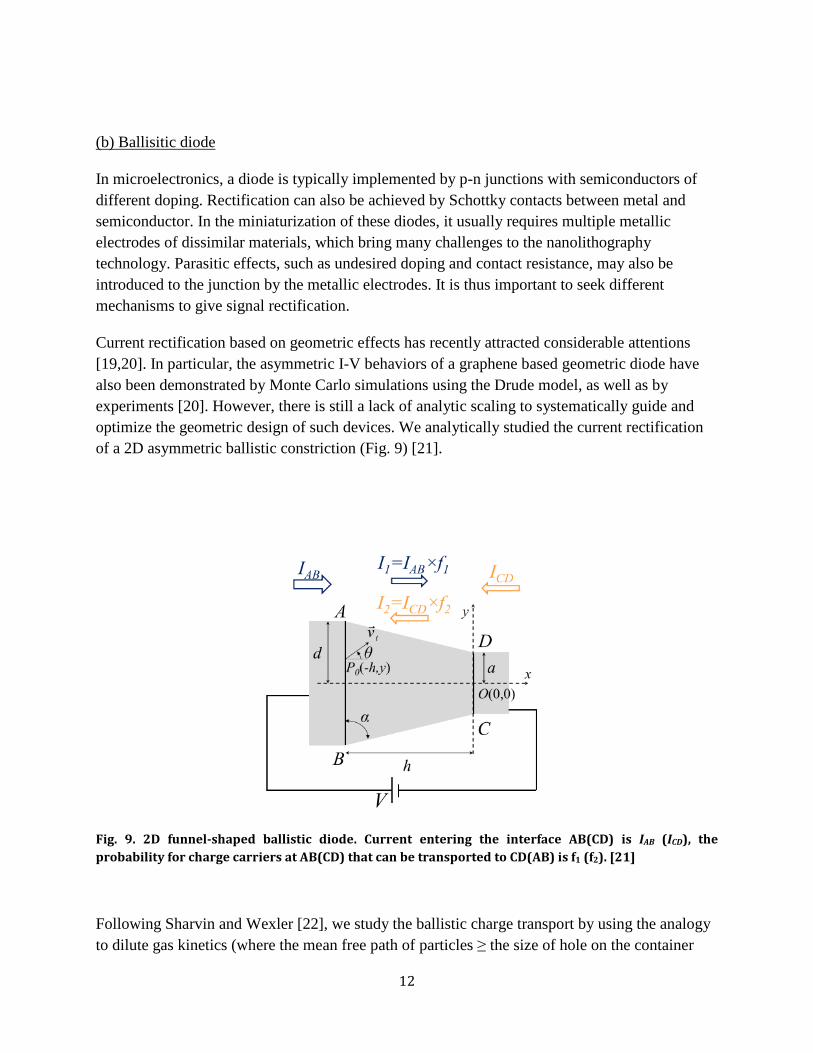
In microelectronics, a diode is typically implemented by p-n junctions with semiconductors of different doping. Rectification can also be achieved by Schottky contacts between metal and semiconductor. In the miniaturization of these diodes, it usually requires multiple metallic electrodes of dissimilar materials, which bring many challenges to the nanolithography technology. Parasitic effects, such as undesired doping and contact resistance, may also be introduced to the junction by the metallic electrodes. It is thus important to seek different mechanisms to give signal rectification.
Current rectification based on geometric effects has recently attracted considerable attentions [19,20]. In particular, the asymmetric I-V behaviors of a graphene based geometric diode have also been demonstrated by Monte Carlo simulations using the Drude model, as well as by experiments [20]. However, there is still a lack of analytic scaling to systematically guide and optimize the geometric design of such devices. We analytically studied the current rectification of a 2D asymmetric ballistic constriction (Fig. 9) [21].
Fig. 9. 2D funnel-shaped ballistic diode. Current entering the interface AB(CD) is IAB (ICD), the probability for charge carriers at AB(CD) that can be transported to CD(AB) is f1 (f2). [21]
Following Sharvin and Wexler [22], we study the ballistic charge transport by using the analogy to dilute gas kinetics (where the mean free path of particles ≥ the size of hole on the container
12
wall). We found that there is an optimal condition under which the I-V asymmetry is maximized, as shown in Fig. 10. Our calculations are verified by Monte Carlo simulations, including the effects of a general drift velocity [21].
Fig. 10. (a) The effective net current, and (b) I-V asymmetry factor η as a function of the angle α, for various incident charge carriers velocity distributions labeled by |g| [21]. In (a), lines are for
analytical theory, and symbols are for Monte Carlo simulations. [21]
2.5 Enhanced power absorption due to surface rougness
This is a joint project with Caltech [24], encouraged by AFOSR Program Managers Drs. Arje Nachman and John Luginsland.
Interaction of electromagnetic waves with rough surfaces is an important topic in science and engineering: surface roughness is known to cause excessive electromagnetic power absorption, and it is one of the major limiting factors to the performance of radio-frequency (RF) cavities and slow wave structures with an impact on communication systems, particle accelerators, and material characterization at microwave frequencies. The enhanced power loss due to surface and interface roughness exerts significant effects on signal integrity of microelectronic circuits.
13
We provided an accurate assessment of the enhanced electromagnetic power absorption caused by small local surface defects consisting of cylindrical bumps or trenches, where we assume the radius a of the defect is much smaller than the free space wavelength λ (a << λ) so that the surface can be considered as locally flat in the absence of the defect.
We first considered problems whereby a semi-cylindrical bump lies on a perfectly conducting surface (PEC) under various electromagnetic incident fields, as shown in Fig. 11. By using the equivalent waveguide approach [23], we analytically calculated the power absorption due to the presence of the bump, by decomposing the incident fields into three modes: (E0, 0), (0, H01), and (0, H02), where the field components are shown in Fig. 11. Figure 12 shows the normalized power absorption of the cylindrical bump associated with the incident electric field E0, and incident magnetic fields H01 and H02 [24]. The analytical calculation is in excellent agreement with that from the numerical code, high-order integral equation method (HIEM), that has recently been developed at Caltech [24]. Thus, our analytical theory provided code validation for HIEM.
Fig. 11. A small semi-cylindrical bump on a perfectly conducting surface whose local wave electric field is E0 and local wave magnetic field H0 in the absence of the bump. [24]
14
Fig. 12. Normalized power absorption from (a), E0, (b), H01, and (c) H02, as a function of δ/a, for various λ/a, where δ is the skin depth of the bump, and λ and a are the incident wavelength and bump radius,
respectively. The analytical calculations (solid lines) are in excellent agreement with those from HIEM (squares), along with other method (Fourier-Bessel expansion, red dots) [24].
15
HIEM code was then used to calculate the power absorption of bump/trench on a finitely conducting flat surface, which cannot be solved analytically. Figure 13 shows the power absorption and the electric field distributions for the bump and trench on finitely conducting surfaces [24]. The incident field decomposition gives unique, penetrating insight into how each component (E0, H01, H02) contributes to the heating on bumps and trenches, which would be virtually impossible in a full scale numerical simulation that includes the total incident fields.
Fig. 13. Normalized power absorption from E0, H01, and H02, as a function of δ/a, and the corresponding electric field distribution inside the surface defect (for δ/a = 0.1, λ/a = 1000), for both
bump and trench on a finitely conducting flat surface [24].
16
2.6 Effects of random manufacturing error on TWT
Surface roughness and inperfect fabrication processes also have detrimental effects on amplifiers. This was studied within this grant. The traveling wave tube (TWT) is a key element in telecommunication systems, satellite-based transmitters, military radar, electronic countermeasures, and communication data links. Variations in performance due to finite fabrication tolerances in the manufacturing process can lower the fraction of TWTs that meet specifications and drive up the cost of manufacturing [25-28]. These errors produce proportionately larger perturbations to the circuit as the circuit size is reduced, and also at high frequencies. Their effects on the small signal gain and output phase are shown in Fig. 14 [26]. A peculiar feature, noted in [26] and [28] is that, in the statistical evaluation of a large number of samples with random errors in the circuit phase velocity, a significant number of these samples show an output gain that is higher than the corresponding error-free tube. We used two very different approach to show that the standard deviation is much larger than the deviation in the mean from an error-free tube, thereby resolving this puzzle [26,28]. The analytical results on the expected gain and phase compare favorably with results from numerical integrations of the governing equation in the absence of space charge, but are found to deviate from the numerical integrations with the inclusion of space charge effects [28].
The effects of the reverse propagating circuit wave was also analyzed [27]. In Ref. [27], we found that reflections may significantly increase the statistical effects on the gain and the output phase. Moreover, gain ripples are introduced [Fig. 15]. Whether this gain ripple can cause absolute instability is being studied.
17
Fig. 14: (a) Mean values of the power and (b) phase at the output relative to the unperturbed values calculated by three different methods. The standard deviation σb measures the variations in circuit phase velocity as a result of random errors. [26]
18
Fig. 15. Small signal gain as a function of frequency for several values of standard deviations of the circuit pitch angle distributions. [27]
19
3.0 Personnel Involvement
Faculty
Y.Y. Lau, Professor
Ronald M. Gilgenbach, Professor
Research Staff
Peng Zhang, Assistant Research Scientist
Graduate Students supported by this Grant
Peng Zhang (graduated Ph.D, now at UM), Wilkin Tang (graduated Ph.D, now at AFRL), Ian Rittersdorf (graduated Ph.D, now at NRL), Michael Johnson, Patrick Wong, Matt Weis.
Undergraduate Students supported by this Grant
Derek Hung, Michael Johnson, David Yu, Patrick Wong.
Invited talks: AFOSR, AFRL (Kirtland), NRL (twice), U Maryland, Rutgers U, Caltech, UC Davis, ICOPS, U Michigan (MIPSIE), Nanyang Technological University (Singapore), Singapore University of Technology and Design.
20
5.0 References
References in bold explicitly acknowledge support from this AFOSR grant.
[1] Peng Zhang, B. Hoff, Y. Y. Lau, D. M. French, J. W. Luginsland, “Excitation of a slow wave structure”, Phys. Plasmas, 19, 123104 (2012).
[2] Review of Federal Programs for Wire System Safety, National Science and Technology Council Final Report, 2000; J. S. Kuzniar and G. A. Slenski, “Wire Integrity Field Survey of USAF Legacy Aircraft”, Defense Technical Information Center, ADP014075, 2001.
[3] R. Holm, Electric Contact, Springer-Verlag, Berlin, ed. 4, 1967.
[4] Peng Zhang, and Y. Y. Lau, “Scaling Laws for Electrical Contact Resistance with Dissimilar Materials”, J. Appl. Phys. 108, 044914 (2010).
[5] Peng Zhang, Y. Y. Lau, W. Tang, M. R. Gomez, D. M. French, J. C. Zier, and R. M. Gilgenbach, “Contact Resistance with Dissimilar Materials: Bulk Contacts and Thin Film Contacts”, Young Investigator Award Paper, Proc. of the 57th IEEE Holm Conf. on Electrical Contacts, pp. 31 – 36, 2011.
[6] Peng Zhang, “Effects of Surface Roughness on Electrical Contact, RF Heating and Field Enhancement,” PhD dissertation, University of Michigan, Ann Arbor, 2012. [7] Peng Zhang, and Y. Y. Lau, “Constriction Resistance and Current Crowding in Vertical Thin Film Contact”, IEEE J. Electron Devices Soc., 1, 83 (2013).
[8] Peng Zhang, Y. Y. Lau, and R. M. Gilgenbach, “Minimization of thin film contact resistance”, Appl. Phys. Lett. 97, 204103 (2010).
[9] M. R. Gomez, D. M. French, W. Tang, Peng Zhang, Y. Y. Lau, and R. M. Gilgenbach, “Experimental validation of a higher dimensional theory of electrical contact resistance”, Appl. Phys. Lett. 95, 072103 (2009).
[10] Peng Zhang, Y. Y. Lau, and R. M. Gilgenbach, “Thin film contact resistance with dissimilar materials”, J. Appl. Phys. 109, 124910 (2011).
[11] Peng Zhang, Y. Y. Lau, and R. S. Timsit, “On the Spreading Resistance of Thin-Film Contacts”, IEEE Trans. Electron Devices, 59, 1936 (2012).
21
[12] Peng Zhang, D. Hung, Y. Y. Lau, “Current Flow in a 3-terminal Thin Film Contact with Dissimilar Materials and General Geometric Aspect Ratios”, J. Phys. D: Appl. Phys., 46, 065502 (2013); Corrigendum, ibid, 46, 209501 (2013).
[13] Y. Y. Lau, D. Chernin, Peng Zhang, and R. M. Gilgenbach, “A Voltage Scale for Electro-Thermal Runaway”, Proc. of IEEE Pulsed Power and Plasma Science, San Francisco, California, 2013.
[14] Peng Zhang, Y. Y. Lau, and R. S. Timsit, “Spreading Resistance of a Contact Spot on a Thin Film”, Proc. of the 59th IEEE Holm Conf. on Electrical Contacts, Newport, RI, 2013.
[15] Peng Zhang, and Y. Y. Lau, “An exact field solution of contact resistance and comparison with the transmission line model”, Appl. Phys. Lett., 104, 204102 (2014).
[16] I. Langmuir and K. B. Blodgett, “Currents Limited by Space Charge between Coaxial Cylinders”, Phys. Rev. 22, 347 (1923). [17] I. Langmuir and K. B. Blodgett, “Currents Limited by Space Charge between Concentric Spheres”, Phys. Rev. 24, 49 (1924). [18] Y. B. Zhu, P. Zhang, A. Valfells, L. K. Ang, and Y. Y. Lau, “Novel scaling laws for the Langmuir-Blodgett solutions in cylindrical and spherical diodes”, Phys. Rev. Lett., 110, 265007 (2013). [19] K. Choi, G. Ryu, F. Yesilkoy, A. Chryssis, N. Goldsman, M. Dagenais, and M. Peckerar, “Geometry enhanced asymmetric rectifying tunneling diodes,” J. Vac. Sci. Technol. B 28, C6O50 (2010).
[20] G. Moddel, Z. Zhu, S. Grover, and S. Joshi, “Ultra high speed graphene diode with reversible polarity,” Solid State Commun. 152, 1842 (2012).
[21] Peng Zhang, and D. Hung, “An analytical model for ballistic diode based on asymmetric geometry”, J. Appl. Phys., 115, 204908 (2014).
[22] Y. V. Sharvin, “A possible method for studying fermi surfaces,” Sov. Phys.-JETP 21, 655 (1965); G. Wexler, “The size effect and the non-local Boltzmann transport equation in orifice and disk geometry,” Proc. Phys. Soc. 89, 927 (1966).
[23] Peng Zhang, Y. Y. Lau, and R. M. Gilgenbach, “Analysis of RF absorption and electric and magnetic field enhancements due to surface roughness”, J. Appl. Phys. 105, 114908 (2009).
[24] C. Perez-Arancibia, Peng Zhang, O. P. Bruno, and Y. Y. Lau, “Electromagnetic power absorption due to bumps and trenches on flat surfaces”, J. Appl. Phys., 116, 124904 (2014).
22
[25] P. Pengvanich, D. Chernin, Y. Y. Lau, J. W. Luginsland, and R. M. Gilgenbach, “Effect of random circuit fabrication errors on small-signal gain and phase in traveling-wave tubes,” IEEE Trans. Electron Devices, vol. 55, no. 3, pp. 916–924, Mar. 2008.
[26] Ian M. Rittersdorf, Thomas M. Antonsen, Jr., David Chernin, and Y. Y. Lau, “Effects of Random Circuit Fabrication Errors on the Mean and Standard Deviation of Small Signal Gain and Phase of a Traveling Wave Tube,” ”, IEEE J. Electron Device Soc. 1, 117 (2013). [27] D. Chernin, I. Rittersdorf, Y. Y. Lau, T. M. Antonsen, and B. Levush, “Effects of Multiple Internal Reflections on the Small-Signal Gain and Phase of a TWT,” IEEE Trans. Electron Devices, vol. 59, no. 5, pp. 1542 –1550, May 2012. [28] I. Rittersdorf, “Effects of random manufacturing errors on the performances of contemporary coherent radiation sources,” PhD Dissertation, University of Michigan, Ann Arbor (2013).