Agyakwa, Pearl and Yang, Li and Arjmand, Elahjeh and Evans, Paul and Corfield, Martin and Johnson, Christopher Mark (2016) Damage evolution in Al wire bonds subjected to a junction temperature fluctuation of 30 K. Journal of Electronic Materials . pp. 1-14. ISSN 1543-186X Access from the University of Nottingham repository: http://eprints.nottingham.ac.uk/33365/1/Damage%20Evolution%20in%20Al%20Wire %20Bonds%20Subjected%20to%20a%20Junction%20Temperature%20Fluctuation%20of %2030%20K.pdf Copyright and reuse: The Nottingham ePrints service makes this work by researchers of the University of Nottingham available open access under the following conditions. This article is made available under the Creative Commons Attribution licence and may be reused according to the conditions of the licence. For more details see: http://creativecommons.org/licenses/by/2.5/ A note on versions: The version presented here may differ from the published version or from the version of record. If you wish to cite this item you are advised to consult the publisher’s version. Please see the repository url above for details on accessing the published version and note that access may require a subscription. For more information, please contact [email protected]
Transcript
Agyakwa, Pearl and Yang, Li and Arjmand, Elahjeh and Evans, Paul and Corfield, Martin and Johnson, Christopher Mark (2016) Damage evolution in Al wire bonds subjected to a junction temperature fluctuation of 30 K. Journal of Electronic Materials . pp. 1-14. ISSN 1543-186X
Access from the University of Nottingham repository: http://eprints.nottingham.ac.uk/33365/1/Damage%20Evolution%20in%20Al%20Wire%20Bonds%20Subjected%20to%20a%20Junction%20Temperature%20Fluctuation%20of%2030%20K.pdf
Copyright and reuse:
The Nottingham ePrints service makes this work by researchers of the University of Nottingham available open access under the following conditions.
This article is made available under the Creative Commons Attribution licence and may be reused according to the conditions of the licence. For more details see: http://creativecommons.org/licenses/by/2.5/
A note on versions:
The version presented here may differ from the published version or from the version of record. If you wish to cite this item you are advised to consult the publisher’s version. Please see the repository url above for details on accessing the published version and note that access may require a subscription.
Damage Evolution in Al Wire Bonds Subjected to a JunctionTemperature Fluctuation of 30 K
PEARL A. AGYAKWA,1,2 LI YANG,1 ELAHEH ARJMAND,1 PAUL EVANS,1
MARTIN R. CORFIELD,1 and C. MARK JOHNSON1
1.—Department of Electrical & Electronic Engineering, The University of Nottingham, UniversityPark, Nottingham NG7 2RD, UK. 2.—e-mail: [email protected]
Ultrasonically bonded heavy Al wires subjected to a small junction tempera-ture fluctuation under power cycling from 40�C to 70�C were investigatedusing a non-destructive three-dimensional (3-D) x-ray tomography evaluationapproach. The occurrence of irreversible deformation of the microstructureand wear-out under such conditions were demonstrated. The observedmicrostructures consist of interfacial and inter-granular cracks concentratedin zones of stress intensity, i.e., near heels and emanating from interfaceprecracks. Interfacial voids were also observed within the bond interior.Degradation rates of ‘first’ and ‘stitch’ bonds are compared and contrasted. Acorrelative microscopy study combining perspectives from optical microscopywith the x-ray tomography results clarifies the damage observed. An estima-tion of lifetime is made from the results and discussed in the light of existingpredictions.
Key words: Aluminum, wire bonds, power cycling, reliability, x-raytomography, high cycle thermal fatigue
INTRODUCTION
Wire bond cracking and lifting-off under thethermomechanical loading experienced during elec-trically-driven load-cycling is extensively reported,and is perhaps the dominant life-limiting wear-outmechanism in power electronic modules. The char-acterisation of wire bond degradation therefore hasan important role to play in achieving reliablelifetime models for power modules.
Accuracy of wire bond lifetime prediction is anessential aspect of the reliable design of powerelectronics components and critical to prognosticsand health management.1,2 It relies on robustexperimental data, which can be sourced fromlaboratory-based accelerated life tests. With recentdevelopments aimed at increased power density andhigher levels of functional integration in powerelectronics, it is not surprising that applications inwhich junction temperatures and/or ambient fluc-tuations exceed 100 K have begun to dominate
reliability research.3–5 However, in the majority ofapplications, including traction motor drives andwind power converters,6,7 small junction tempera-ture ranges are the norm, and accurate lifetimeprediction data for such operation regimes isequally important. Rapid degradation of intercon-nects with catastrophic consequences may be a lessfrequent occurrence in small DT applications; how-ever, the associated consequences of unavailabilityand unscheduled maintenance are highly undesir-able. Reliable lifetime models for such applicationscan enable a prognostics and health managementapproach to asset management, which negates theeconomic losses associated with unnecessary/pre-mature refits or unscheduled maintenance.
There is a widely held opinion that the thermo-mechanical stresses imposed by DTs of 40 K andbelow are so small that there is virtually no wear-out, and thus the wire bonds are expected toperform in perpetuum.6,8 In,6 it was suggested thatthermomechanical fatigue of Al wire bonds wouldfollow a trend observed during load-controlledbending fatigue of 99.5% Al. The belief is thatdeformation under such small loads is essentially(Received May 10, 2015; accepted April 6, 2016)
Journal of ELECTRONIC MATERIALS
DOI: 10.1007/s11664-016-4519-0� 2016 The Author(s). This article is published with open access at Springerlink.com
‘elastic’, leading to the conclusion of infinite lifetimeunder small junction temperature fluctuations.8,9
However, the authors are unaware of any experi-mental evidence to substantiate these hypotheses.
For applications which ordinarily experience‘‘small’’ temperature fluctuations (i.e. small DTs),accelerated testing is often relied upon to provideservice life estimations. However, this approach hasa major drawback, namely the existing lack ofexperimental evidence about degradation mecha-nisms under such low loads, which are at risk ofbeing concealed by the mechanisms produced by thelarger DTs often used to generate the informationneeded. Typically, wire bond lifetimes are interpo-lated from standard Coffin–Manson curves popu-lated with data generated using much largerDTs.10–12 This may be an entirely valid approach;nonetheless, its validity needs to be assessedthrough actual experimental data.
Another important issue regards the limitationsof a number of life assessment experimentalapproaches, such as shear force evaluation. Thejustification for the use of shear force is that itdecreases to reflect the reduction in bonded areathat accompanies crack propagation during cycling.However, there is variation in results betweendifferent wires because of inherent error in mea-surement and because of the inherent probabilisticnature of damage evolution. Because each datapoint originates from a wire bond that is essentiallysacrificed, shear testing is insensitive to the verysmall amounts of degradation which may be typicalunder small DT mission profiles. Such smallchanges may be lost in the statistical spread andmisconstrued as ‘no degradation’. Furthermore, areduction in shear (and pull) strength may also beattributable to a change in a material’s yieldstrength. This fact becomes even more pertinent ifthe temperature range is large and involves highjunction temperatures equal to or greater than0.3Tm, as significant microstructural restorationcan occur.13 This means that a wire bond thatsoftens over time but remains adequately intactmay be wrongly characterised as lifting off.
Wire bond lifetime evaluation data may alsoinvolve forward voltage measurements as a func-tion of the number of cycles. This approach hasbeen shown to lack sufficient sensitivity over thecritical wear-out period, as it only begins to detectdegradation once lift-offs have already started tooccur.14 The observation of changes in wire resis-tance using a four-point probing approach has beenproposed as an effective way of monitoring degra-dation at the wire bond interfaces,15 however, novalidation through correlation with experimentallyobserved damage has been shown. Although sheartests and metallurgical cross-sections have greatersensitivity, their destructive nature does not allowthe same specimen to be monitored and evaluatedover an entire test period. Pertinent information
relating to the inherent differences due to differentdegradation patterns in each wire is thereforeforfeited.
Computer tomography (CT) has been around for acouple of decades, but until recently, it was essen-tially confined to medical diagnostics applications.In recent years, however, suitable, higher energyCT systems have been developed for non-destructiveevaluation of the internal structure of engineeringmaterials and structures.16 This has been helpedsignificantly by recent developments in computingpower. A typical CT system consists of an x-raysource and a detector. Several x-ray images orprojections of a sample mounted onto a rotatingstage are acquired by a detector. These images aremathematically reconstructed to obtain a three-dimensional (3-D) map of the sample. Multiple‘virtual’ cross-sections (or slices) can be obtained inany plane of interest. Because a specific specimencan be evaluated repeatedly over its lifetime, anexact picture of the evolution of damage duringoperation can be obtained and observed three-dimensionally. With high enough spatial resolution,near-microstructural characteristics can beobserved. In cases such as wire bond degradationunder small temperature fluctuations where testing‘to failure’ may be infeasible due to time constraints,a prioi knowledge of the condition of the interfaceobtained through tomography can be evaluatedagainst datasets obtained at later stages of life.Regardless of the temporal resolution of the CTdatasets, a reasonable estimation of wear-out rate ispossible without the need to test to failure. Addi-tionally, the possibility of three-dimensional scru-tiny of degradation as it develops can provide newperspectives and crystallise our understanding ofwire bond wear-out. Although wire bond lift-off dueto thermal cycling fatigue is well documented,17–19
there are complexities in the degradation mecha-nisms that are not yet fully elucidated. The lack ofclarity is attributable to several factors, includingthe ambiguous nature of the wire bonding mecha-nism itself, over which there are still a number ofviews.20–26 This is compounded by the fact that theconcept of fatigue damage generally lags behindother wear out phenomena in terms of the degree ofunderstanding and consensus of relevant mecha-nisms of initiation, accumulation, and how thesemay be quantified.27–29 In view of all these factors,the additional insight that can be gained from a‘same sample’ x-ray computed tomography study isinstrumental.
In this paper, supported by the x-ray CT non-destructive evaluation approach, we examine whatactually happens under a small scale temperaturefluctuation by observing the same wire bonds overtime, and we weigh our observations up againstexisting knowledge and theories regarding degra-dation under small junction temperaturefluctuations.
Agyakwa, Yang, Arjmand, Evans, Corfield, and Johnson
EXPERIMENTAL PROCEDURES
The test specimens employed in this study weremanufactured externally by Dynex SemiconductorLtd. They consisted of eight 99.999% (5N) purealuminum wires, 375 lm in diameter, bonded ontosilicon diodes. The silicon diodes had been previ-ously soldered down onto Direct Bonded Copper(DBC) substrates.
Power Cycling Experimental Set-Up
The power cycling equipment uses a switchedcurrent supplied by a constant current power supplyto heat a set of sample ‘coupons’ whilst cooling isprovided by a cold-plate connected to a temperature-controlled water chiller. Each coupon consists of asingle diode die soldered and wire bonded onto asubstrate tile, as shown in Fig. 1. A central mea-surement spot painted on to each diode (an emis-sivity reference surface) facilitates junctiontemperature measurement by close-focus infrared(IR) sensor lenses. The heating current is applied orremoved automatically when the temperature dropsbelow or rises above specified limits. The heatingcurrent is controlled using a set of low-resistancebypass switches (MOSFETs), one in parallel witheach coupon, which when activated divert theheating current away from the coupon. The couponis constantly cooled (at constant temperature) usinga heatsink and recirculating chiller. In this exper-iment, the power cycling regime consisted of apply-ing a constant current of about 32 A. Each cycle hada period of 7 s and a temperature amplitude ofapproximately 30 K from 40�C to 70�C. A snapshotof the temperature profile for the coupons is given inFig. 2.
X-ray Tomography Imaging and Analysis
The development of discontinuities (openings,voids, and cracks) at the interface between wirebonds and the silicon dies during power cycling has
been studied. The wire bonds were imaged prior topower cycling (in the ‘‘as-bonded’’ condition) in orderto provide a basis for comparison. The same wireswere subsequently imaged at several stagesbetween zero and 1.2 million cycles. The work wascarried out on an Xradia Zeiss Versa XRM500 CTsystem with a maximum electron acceleration of160 kV.
A source voltage of 80 kV was used and a 4Xobjective detector was selected. Specimen-to-sourceand specimen-to-detector distances varied slightlywith each set-up but were typically 55 mm and145 mm, respectively. An appropriate filter wasapplied to monochromate the x-ray beam andminimise artefacts. A 2 9 2 camera binning modewas used to capture the images at exposure timesper projection ranging between 18 s and 30 s. Theseparameters allowed a spatial resolution of about1.6 lm to be achieved, which was considered ade-quate for the resolution of cracks and openings. Foreach specimen, a total of up to 2401 projections wereacquired over a rotation span of 180 degrees.
Up to twelve tomography datasets were acquiredover 1,245,202 cycles. A second wire-bonded testcoupon was imaged after 2.1 million cycles and
Fig. 1. (a) Test coupon and (b) power cycling set-up.
Fig. 2. Snippet of the temperature profile for the test coupons.
Damage Evolution in Al Wire Bonds Subjected to a Junction Temperature Fluctuation of 30 K
cross-sectioned to provide correlative analysisthrough optical metallography and scanning elec-tron microscopy (SEM).
The 2401 projection images were reconstructedusing Xradia 3D Reconstructor software, which usesa filtered back projection algorithm. The reconstruc-tion procedure included determining the centre-shift, that is, the offset in pixels of the rotationalaxis from the centre column of the detector, andoccasionally applying a correction for beam harden-ing. The tomography datasets were visualised andmultiple virtual cross-sections were obtained usingXradia-Zeiss 3D Viewer. Further visualisation,semi-quantitative area, and volume analyses werecarried out using the FIJI software package. Asimple methodology was employed to quantify theevolution of damage in the first bonds. This involvedestimation of the contact area resolvable withinrepresentative two-dimensional greyscale TIFFimages parallel to the bond interface (in the X–Yplane). This was performed using the polygonselection tool within FIJI software. The exteriorsurfaces of the bonds were also studied usingscanning electron microscopy.
Metallurgical Cross-Sections for Optical Mi-croscopy
A separate sample, also subjected to 2.1 millionpower cycles under the same regime, was sectionedto provide specimens of the X–Y plane and Y–Zplane. These were mounted in edge-retentive epoxyresin and cured at room temperature for 24 h. Theywere then slowly and carefully mechanically pol-ished on a Buehler Metaserv automatic polisher.This involved successive grinding with 1200, 2500,and 4000 grit silicon carbide papers, and 3 lm and1 lm diamond slurries, all the while ensuring thatdamage from successive grinding/polishing stepswas completely removed before progressing. A finalpolish was achieved using a 0.06 lm colloidal silicasuspension.
RESULTS AND DISCUSSION
Description of the Evolving Damage
The regions of interest are indicated in Fig. 3 in athree-dimensional volume rendered overview of atypical specimen and consists of pairs of stitch andfirst bonds. Alongside this, a two-dimensional
Fig. 3. Figure showing (a) the test coupon, (b) a 3-D rendered overview, (c) a 2-D virtual cross-section of tomography imaging zones, and (d) a3-D rendered view of a typical detailed tomography zone.
Agyakwa, Yang, Arjmand, Evans, Corfield, and Johnson
virtual cross-section is presented indicating theregions of interest in the plane of the diode andshows the orientation of the sample with referenceto the direction of the incident x-rays. Two bondinterfaces, i.e., one ‘first’ bond and one ‘stitch’ bond,
are selected for detailed scrutiny; these are circledin Fig. 3.
First Bonds
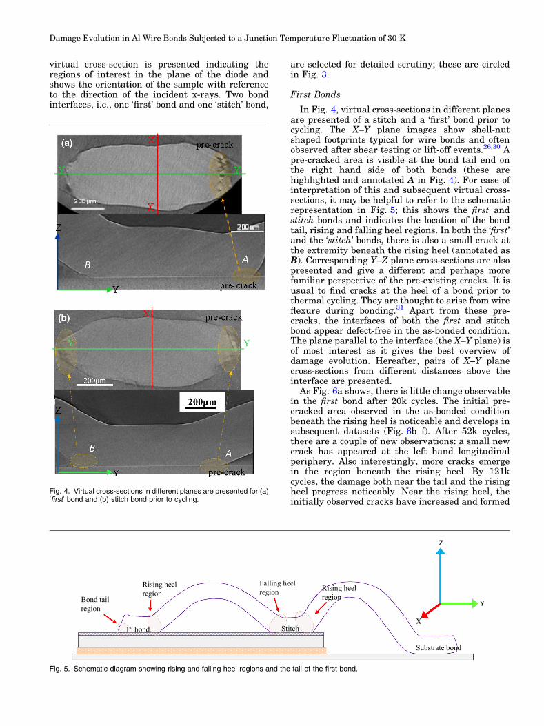
In Fig. 4, virtual cross-sections in different planesare presented of a stitch and a ‘first’ bond prior tocycling. The X–Y plane images show shell-nutshaped footprints typical for wire bonds and oftenobserved after shear testing or lift-off events.26,30 Apre-cracked area is visible at the bond tail end onthe right hand side of both bonds (these arehighlighted and annotated A in Fig. 4). For ease ofinterpretation of this and subsequent virtual cross-sections, it may be helpful to refer to the schematicrepresentation in Fig. 5; this shows the first andstitch bonds and indicates the location of the bondtail, rising and falling heel regions. In both the ‘first’and the ‘stitch’ bonds, there is also a small crack atthe extremity beneath the rising heel (annotated asB). Corresponding Y–Z plane cross-sections are alsopresented and give a different and perhaps morefamiliar perspective of the pre-existing cracks. It isusual to find cracks at the heel of a bond prior tothermal cycling. They are thought to arise from wireflexure during bonding.31 Apart from these pre-cracks, the interfaces of both the first and stitchbond appear defect-free in the as-bonded condition.The plane parallel to the interface (the X–Y plane) isof most interest as it gives the best overview ofdamage evolution. Hereafter, pairs of X–Y planecross-sections from different distances above theinterface are presented.
As Fig. 6a shows, there is little change observablein the first bond after 20k cycles. The initial pre-cracked area observed in the as-bonded conditionbeneath the rising heel is noticeable and develops insubsequent datasets (Fig. 6b–f). After 52k cycles,there are a couple of new observations: a small newcrack has appeared at the left hand longitudinalperiphery. Also interestingly, more cracks emergein the region beneath the rising heel. By 121kcycles, the damage both near the tail and the risingheel progress noticeably. Near the rising heel, theinitially observed cracks have increased and formed
Fig. 4. Virtual cross-sections in different planes are presented for (a)‘first’ bond and (b) stitch bond prior to cycling.
1st bond Stitch
Substrate bond
Rising heel region
Falling heel region Rising heel
regionBond tail region
Z
Y
X
Fig. 5. Schematic diagram showing rising and falling heel regions and the tail of the first bond.
Damage Evolution in Al Wire Bonds Subjected to a Junction Temperature Fluctuation of 30 K
networks, and as Fig. 6d shows, this network ofcracks extends a few microns above the interfaceinto the bulk of the wire and appear to be inter-granular in nature, as expected. Interestingly, the
virtual cross-sections after 865k cycles show theemergence of a few small but deep voids within theinterior of the interface. After 1245k cycles, yetmore voids develop in a different region (Fig. 6f).
Fig. 6. Virtual cross-sections of the ‘first’ bond in the X–Y plane (parallel to the bonding interface), showing damage evolution in the same sampleat different distances from the bond interface (as indicated) with increasing number of cycles. (a1, a2) zero cycles, (b1, b2) 20,000 cycles, (c1, c2)52,000 cycles, (d1, d2) 121,000 cycles, (e1, e2) 865,000 cycles, (f1, f2) 1,245,000 cycles.
Agyakwa, Yang, Arjmand, Evans, Corfield, and Johnson
Besides the development of voids, the fine cracknetworks at the extremity near the rising heel areyet more prominent now extending over anincreased depth of 16 lm into the bulk of the wire.A series of virtual cross-sections in the Y–Z plane ispresented in Fig. 7 and also shows these developingcracks. Crack development is notably more rapid atthe rising heel end than at the bond tail end. Thecracks may extend further than is resolvable inthese images.
Stitch Bonds
As with the first bond, apart from small areas ofdiscontinuity at the extreme ends, the interior of thestitch bond is more or less featureless in the as-bonded condition (see Fig. 8a–d). Cracks, however,seem more prominent earlier, at 20k cycles, asFig. 8b shows. Additionally, unlike the first bond,
the development of cracks is rapid at both extremeends of the bond (both rising and falling heel ends,refer to the schematic diagram in Fig. 5) although itis more pronounced at the rising heel side. Adifference in the nature of damage between thetwo ends is observable. Damage development in therising heel is much like that in the region beneaththe rising heel of the first bond in that it ischaracterised by networks of cracks, which formbranches and extend as the number of cyclesincreases. On the other hand, the development ofcracks at the falling heel side is less striking.
Interpretation and Analysis of TomographyResults
In order to explain the macrostructural changesobserved, it is helpful to recall bond wiremicrostructures, and how they evolve during
Fig. 7. Virtual cross-sections of the ‘first’ bond in the Y–Z plane at mid thickness, showing crack growth in the same sample with increasingnumber of cycles (enlarged rising heel side cracks are shown on the right) (a) zero cycles, (b) 52,000 cycles, (c) 865,000 cycles, (d) 1,245,000cycles.
Damage Evolution in Al Wire Bonds Subjected to a Junction Temperature Fluctuation of 30 K
cycling. The bonding process by which wire bondinterconnections are produced utilises ultrasonicenergy and mechanical force, which both deform thewire and facilitate plastic flow across the interface.
The work done during bonding leads to the gener-ation of defects, i.e., dislocations, and a highlyheterogeneous and deformed microstructure.32 Thismicrostructure has been characterised as deformed
Fig. 8. Virtual cross-sections of the ‘stitch’ bond in the X–Y plane (parallel to the bonding interface), showing damage evolution in the samesample at different distances from the bond interface (as indicated) with increasing number of cycles. (a1, a2) zero cycles, (b1, b2) 20,000 cycles,(c1, c2) 52,000 cycles, (d1, d2) 121,000 cycles.
(a) (b)
σ
Silicon die
Al wireσ
Silicon die
Al wire
Hea�ng (Current On): Compressive stress
Cooling (Current Off): Tensile stress
Al top metallisa�on
Fig. 9. Schematic diagram showing the regions of compression/tension during cycling (after Onuki et al.4).
Agyakwa, Yang, Arjmand, Evans, Corfield, and Johnson
elongated grains with a high degree of misorienta-tion near the interface25 relative to the direction ofthe applied stress, suggestive of an increasedamount of stored energy.33 The rearrangement orannihilation of these defects will serve to minimisethe energy of the system and is the origin of thethermodynamic driving force for recrystallisation.Recrystallisation occurs partially at the time ofbonding, as the bonding deformation is high enoughto bring about the nucleation of new grains.34
During the operation of power modules, heat isgenerated within the semiconductor chips andswitching leads to repeated heating and cooling.The aluminum wire and silicon chip expand atdifferent rates, and this generates shear stresses attheir interface. Given sufficient thermal energy,high stacking fault energy materials like aluminumreadily undergo recovery (even at room tempera-ture,33), during which dislocations are reconfiguredinto a lower energy state. Therefore, microstruc-tural restoration under even this small temperaturecycling range and relatively low maximum junctiontemperature would be unsurprising.
Microstructurally, the bond interface is charac-terised by distinctive gradients: the metallisationlayer is usually distinct from the wire and made upof very fine deformed grains; directly above, there isa region of small recrystallised grains, and furtheraway into the bulk, there are more randomlyoriented grains with texture similar to that of theas-received wire.25,34 The shear stresses generatedat the interface during thermal cycling are concen-trated at the extreme ends of the bonded area.Driven by the release of energy, cracks develop andpropagate toward the centre of the bond and in aregion a few microns above the metallisationformerly characterised by fine recrystallised grains,and a region with reported high grain misorienta-tion.25,34 This would be in agreement with thefindings of this study, in which undulating cracksat least 18 lm above the interface are observed andwhich advance toward the centre as the number of
cycles increases. High angle grain boundaries areassociated with the preferential initiation and prop-agation of fatigue cracks in fcc polycrystals.35,36
The bond peripheries and extremities are suscep-tible to damage for a number of reasons. Duringbonding, as the wire flexes with the movement of thebond-head during loop formation damage occurs,particularly at the rising heel. Further alterationand deformation of microstructure in these regionsoccurs as a result of power cycling, during which theregion above the heel experiences alternate com-pression and tension due to heating and cooling6 (seeFig. 9). Finite element simulations of bond wiresduring thermal cycling confirm stress concentrationat the heel.37,38 During active power cycling, anexacerbation of this stress state may occur as aresult of forces due to the electromagnetic interac-tion between the wires leading to lateral displace-ments.39 Concurrently, the concentration of stress inthe aforesaid regions may mean a greater propensityfor microstructural restoration in order to achieve aminimised energy state. Such restoration may cre-ate regions of localised low yield strength, leading tolocalised mismatches in the Taylor factor of grains.25
This may explain the observed concentration ofevolving damage in the vicinity of the bond heels,and the rising heels in particular, where flexingduring power cycling may be more intense.6
Another factor to consider is the heterogeneousdistribution of current on the die and within thewires.40,41 This may explain the different rates ofdegradation observed at different locations.
Void Formation and Growth
In a previous article,42 we reported the appear-ance of interfacial voids in a same-sample tomogra-phy study during thermal cycling from �55�C to190�C, in which voids were observed to grow and/orcoalesce to form larger areas of discontinuity. It isplausible that these voids were in existence a prioriand may have originated from regions of partial
Fig. 10. Focused ion beam cross-sectional image of an as-bonded wire (a), showing interfacial oxide particles and voids (b) from Loh et al.44
Damage Evolution in Al Wire Bonds Subjected to a Junction Temperature Fluctuation of 30 K
bonding beyond the resolution limits of the tomog-raphy datasets. Certainly, voids have been widelyobserved at the interfacial line in as-bonded wiresand attributed to the presence of oxide debris andextraneous particles, and linked to bonding condi-tions.43,44 The focused ion beam (FIB) cross-sec-tional image in Fig. 1044 is such an example andclearly shows a line of particles between a horizon-tal band of fine, metallisation grains and largergrains belonging to the bulk wire. The actualnucleation of new voids under the relatively benigntemperature cycling conditions of this study is also
feasible, considering the homologous temperaturesinvolved (i.e., 0.34–0.37Tm). While the thermallyactivated transport of atoms over time is certainlyviable, we know that the high strain [due tocoefficient of thermal expansion (CTE) mismatchat the interface in this case] can also drive themovement of atoms away from voids by dislocationloops, resulting in a gradual enlargement of the saidvoids.45 Thus, strain-induced void growth isstrongly linked to dislocation density.46 This straincan also provide the driving force for grain bound-ary nucleation and grain growth.47
Fig. 11. Virtual cross-sections of a ‘stitch’ bond subjected to 2.1 million cycles, showing damage in the X–Y plane at different distances (a-c) (asindicated) from the bonding interface in the Y–Z plane image (d).
Agyakwa, Yang, Arjmand, Evans, Corfield, and Johnson
Correlative Microscopy
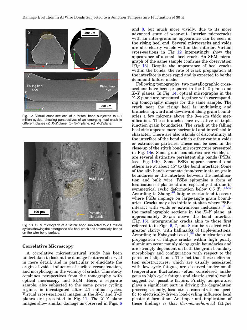
A correlative microstructural study has beenundertaken to look at the damage features observedin more detail, and in particular to elucidate theorigin of voids, influence of surface reconstruction,and morphology in the vicinity of cracks. This studycombines perspectives from the tomography withoptical microscopy and SEM. Here, a separatesample, also subjected to the same power cyclingregime, is investigated after 2.1 million cycles.Virtual cross-sectional images in the X–Y and Y–Zplanes are presented in Fig. 11. The X–Y planeimages show similar damage as observed in Figs. 6
and 8, but much more vividly, due to its moreadvanced state of wear-out. Interior microcrackswith an inter-granular appearance can be seen inthe rising heel end. Several microcracks and voidsare also clearly visible within the interior. Virtualcross-sections in Fig. 12 interestingly show theappearance of a small heel crack. An SEM micro-graph of the same sample confirms the observation(Fig. 13). Despite the appearance of heel crackswithin the bonds, the rate of crack propagation atthe interface is more rapid and is expected to be thedominant failure mode.
Following tomography, two metallographic cross-sections have been prepared in the Y–Z plane andX–Y planes. In Fig. 14, optical micrographs in theY–Z plane are presented, together with correspond-ing tomography images for the same sample. Thecrack near the rising heel is undulating andbranches upward and downward along grain bound-aries a few microns above the 3–4 lm thick met-allisation. These branches are evocative of triplejunction grain boundaries. The crack at the fallingheel side appears more horizontal and interfacial incharacter. There are also islands of discontinuity atthe interface of the bond which either contain voidsor extraneous particles. These can be seen in theclose-up of the stitch bond microstructure presentedin Fig. 14c. Some grain boundaries are visible, asare several distinctive persistent slip bands (PSBs)(see Fig. 14b). Some PSBs appear normal andothers are at about 45� to the bond interface. Someof the slip bands emanate from/terminate on grainboundaries or the interface between the metallisa-tion and bulk wire. PSBs epitomise a form oflocalisation of plastic strain, especially that due tosymmetrical cyclic deformation below 0.5 Tm.48,49
According to Zhang,48 fatigue cracks tend to occurwhere PSBs impinge on large-angle grain bound-aries. Cracks may also initiate at sites where PSBsinteract with voids or extraneous inclusions.36 Inthe metallographic sections in the X–Y plane, atapproximately 20 lm above the bond interface(Fig. 15), intergranular cracks akin to those firstreferred to in Figs. 6, 7, and 8 can be resolved withgreater clarity, with hallmarks of triple-junctions.According to Kobayashi et al.,36 the nucleation andpropagation of fatigue cracks within high purityaluminum occur mainly along grain boundaries andare strongly dependent on both the grain boundarymorphology and configuration with respect to thepersistent slip bands. The fact that these deforma-tion substructures, which are usually associatedwith low cycle fatigue, are observed under smalltemperature fluctuation (often considered analo-gous to high cycle fatigue and elastic strain) wouldsuggest two possible factors. Firstly, temperatureplays a significant part in driving the degradationprocess; secondly, local stress concentrations speci-fic to electrically-driven load-cycling influence localplastic deformation. An important implication ofthese findings is that thermomechanical fatigue
Fig. 12. Virtual cross-sections of a ‘stitch’ bond subjected to 2.1million cycles, showing perspectives of an emerging heel crack indifferent planes (a) X–Z plane, (b) X–Y plane, (c) Y–Z plane.
Fig. 13. SEM micrograph of a ‘stitch’ bond subjected to 2.1 millioncycles showing the emergence of a heel crack and several slip bandson the wire bond surface.
Damage Evolution in Al Wire Bonds Subjected to a Junction Temperature Fluctuation of 30 K
Fig. 14. Virtual cross-section in the (a) Y–Z, (b) X–Y and (c) X–Z planes of ‘stitch’ bond subjected to 2.1 million cycles, and corresponding opticalmicrographs following metallographic preparation in the Y–Z plane (d, e).
Fig. 15. Metallographic cross-section in the X–Y plane (parallel to the bond interface) of a ‘first’ bond subjected to 2.1 million cycles.
Agyakwa, Yang, Arjmand, Evans, Corfield, and Johnson
requires an approach different from that of mechan-ical fatigue. This is especially noteworthy in relationto the interpretation of isothermal mechanicalfatigue tests performed in lieu of thermomechanicaltests (e.g., Refs. 9 and 50), as such tests are unableto account for the influence of thermally drivenmicrostructural phenomena, which clearly occureven under such small loads.
Estimation of Lifetime
In Fig. 16, the evolution of damage within thefirst bond is expressed as the fractional contact areaas a function of the number of cycles. The fraction ofarea bonded fc is close to 1 in the as-bondedcondition and tends to zero with an increasingnumber of cycles. Linear regression analysis of thedata forecasts lift-off at approximately 10 millioncycles. This agrees well with that of Ramminger,based on the Coffin–Manson model51 (see Fig. 17a).However, our estimation deviates markedly fromthe prediction of Onuki et al.6 (see Fig. 17b). Theestimation in Ref. 6 was based on the behaviour ofaluminum under load-controlled bending and pre-dicted nearly infinite lifetimes below 40 K. Onereason for the disagreement of Onuki et al.’s pre-diction with our experimental data may be thattemperature, strain-rate dependence of the wire’sresponse to mechanical stress, and local stressconcentrations associated with crack tips and voidsare not reflected in load-controlled fatigue data.9
This underscores the need for life assessmentmodels, which are not based solely on conventionalunderstanding of isothermal mechanical fatigue,but incorporate the influence of temperature andtime-dependent microstructural parameters.
SUMMARY AND CONCLUSIONS
In this paper, 3-D x-ray microscopy has beenutilised to visualise the evolution of cracks andvoids in ultrasonically bonded aluminum wiressubjected to a small junction temperature fluctua-tion from 40�C to 70�C under active power cycling.The development of degradation is demonstrable.Cracks were observed to emanate from the extremeedges of the bonds and advance towards the centrein an interfacial fashion. In addition, intergranularcracks were observed to occur primarily in thevicinity of the rising heel side of both the first andstitch bonds. Furthermore, micro-defects, whichmay be voids or micro-cracks, have been observedwithin the interior, growing and increasing in
Fig. 16. Fractional bonded area bonded versus number of cycles forfirst bond.
Fig. 17. Comparison of life estimation from fractional contact areawith predictions in the literature (a) courtesy of Ramminger51
(b) Onuki et al.6
Damage Evolution in Al Wire Bonds Subjected to a Junction Temperature Fluctuation of 30 K
number with an increasing number of cycles. Anestimation of lifetime made from measuring contactarea as a function of number of cycles, together withthe observed microstructural features, suggest thattemperature and local stress concentrations atcrack tips and voids play a significant part indriving the degradation process.
ACKNOWLEDGEMENTS
The authors gratefully acknowledge the supportof the Innovative Electronics Manufacturing Re-search Centre (IeMRC) funded by the UK Engi-neering and Physical Sciences Research Council(EPSRC) through research Grant EP/H03014X/1.The authors also wish to thank Dynex Semicon-ductor Ltd. for providing the wire bond samples.
OPEN ACCESS
This article is distributed under the terms of theCreative Commons Attribution 4.0 InternationalLicense (http://creativecommons.org/licenses/by/4.0/),which permits unrestricted use, distribution, andreproduction in any medium, provided you giveappropriate credit to the original author(s) and thesource, provide a link to the Creative Commons li-cense, and indicate if changes were made.
REFERENCES
1. M. Musallam, C.M. Johnson, C.Y. Yin, H. Lu, and C. Bai-ley, in 13th International Power Electronics and MotionControl Conference (2008), pp. 76–83.
2. B. Ji, V. Pickert, W. Cao, and B. Zahawi, IEEE Trans.Power Electron. 28, 5568 (2013).
3. Y. Yamada, Y. Takaku, Y. Yagi, I. Nakagawa, T. Atsumi,M. Shirai, and I. Ohnuma, Microelectron. Reliab. 47, 2147(2007).
4. R. Bayerer, Microelectron. Reliab. 50, 1715 (2010).5. R. Amro and J. Lutz, in Proc. 2004 35th Annual IEEEPower
Electronics Specialists Conference (2004), pp. 2593–2598.6. J. Onuki, M. Koizumi, and M. Suwa, IEEE Trans. Adv.
Pack. 23, 108–112 (2000).7. J. Wu, L. Zhou, P. Sun, and X. Du, in Proc. Electronics and
Application Conference and Exposition (PEAC), 2014International (2014), pp. 41–48.
8. K. Sasaki and N. Iwasa, in Proc. 20th Int. Symp. PowerSemicond. Devices ICs (2008), pp. 181–184.
9. G. Khatibi, M. Lederer, B. Weiss, T. Licht, J. Bernardi, andH. Danninger, Proc. Eng. 2, 511 (2010).
10. M. Held, P. Jacob, G. Nicoletti, P. Scacco, and M.H. Poech,Int. J. Electron. 86, 1193 (1999).
11. U. Scheuermann and R. Schmidt, Microelectron. Reliab.53, 1687 (2013).
12. P. Cova and F. Fantini, Microelectron. Reliab. 38, 1347(1998).
13. P.A. Agyakwa, V.M.F. Marques, M.R. Corfield, J.F. Li, L.Yang, and C.M. Johnson, J. Electron. Mater. 42, 537 (2013).
14. L. Zhou, S. Zhou, and M. Xu, Microelectron. Reliab. 53, 282(2013).
15. K.B. Pedersen, P.K. Kristensen, V. Popok, and K. Peder-sen, IEEE Trans. Power Electron. 30, 2405 (2015).
16. P.J. Withers and M. Preuss, Annu. Rev. Mater. Res. 4, 81(2012).
17. M. Ciappa, Microelectron. Reliab. 42, 653 (2002).
18. I. Lum, M. Mayer, and J. Zhou, J. Electron. Mater. 35, 433(2006).
19. S. Ramminger, S.P. Turkes, and G. Wachutka, Microelec-tron. Reliab. 38, 1301 (1998).
20. J.E. Krzanowski, IEEETrans. Compon. Hybrid 13, 176 (1990).21. I. Lum, M. Mayer, and Y. Zhou, J. Electron. Mater. 35, 433
(2006).22. K.C. Joshi, Weld. J. 50, 840 (1971).23. R. Pohlman and E. Lehfeldt, Ultrasonics 4, 178 (1966).24. N. Murdeshwar and J.E. Krzanowski, Metall. Mater.
Trans. A 28, 2663 (1997).25. M.S. Broll, U. Geißler, J. Hofer, S. Schmitz, O. Wittler, and
36. S. Kobayashi, T. Inomata, H. Kobayashi, S. Tsurekawa,and T. Watanabe, J. Mater. Sci. 43, 3792 (2008).
37. H. Lu, W.-S. Loh, C. Bailey, and C.M. Johnson, in 3rdInternational Microsystems, Packaging, Assembly & CircuitsTechnology Conference (2008), pp. 22–24. doi:10.1109/IMPACT.2008.4783883.
42. P.A. Agyakwa, L. Yang, M.R. Corfield, and C.M. Johnson,in Proc. 8th International Conference on Integrated PowerSystems (CIPS) (2014).
43. G. Khatibi, B. Weiss, J. Bernadi, and S. Schwarz, J. Elec-tron. Mater. 41, 3436 (2012).
44. W.-S. Loh, S.C. Hogg, R.J. Ikujeniya, M.R. Corfield, P.Agyakwa, and C.M. Johnson, in Proc. International Con-ference on High Temperature Electronics (HiTEC) (Albu-querque, 2008).
45. C. Mi, D.A. Buttry, P. Sharma, and D.A. Kouris, J. Mech.Phys. Solids 59, 1858 (2011).
46. P. Shanthraj and M.A. Zikry, Int. J. Plast. 34, 154 (2012).47. R.R. Keller, R.H. Geiss, N. Barbosa, A.J. Slifka, and D.T.
Read, Metall. Mater. Trans. A 38, 2263 (2007).48. Z.J. Zhang, P. Zhang, L.L. Li, and Z.F. Zhang, Acta Mater.
60, 3113 (2012).49. P. Lukas and L. Kunz, Philos. Mag. 84, 317 (2004).50. G. Khatibi, W. Wroczewski, B. Weiss, and T. Licht, Mi-
croelectron. Reliab. 48, 1822 (2008).51. S. Ramminger, Siemens AG, Munich, Germany, personal
communication, 2008.
Agyakwa, Yang, Arjmand, Evans, Corfield, and Johnson