141
Aerial Intruder Removal – System for Tracking and Rendering Ineffective Knavish Enemies AIR-STRIKE Group 13 Kevin Chau Scott Greenwald Andrew Kirk Christopher Walls May 1st, 2015

Aerial Intruder Removal – System for Tracking and Rendering Ineffective Knavish Enemies
AIR-STRIKE Group 13
Kevin Chau Scott Greenwald Andrew Kirk Christopher Walls
May 1st, 2015

i
Table of Contents 1.0 Executive Summary ..................................................................................... 1
2.0 Project Description ....................................................................................... 3
2.1 Project Motivation and Goals ...................................................................... 3
2.2 Objectives ................................................................................................... 3
2.3 Project Requirements and Specifications .................................................... 4
2.3.1 Microcontroller Requirements ............................................................... 5
2.3.1.1 Handling Input from Cameras ........................................................ 5
2.3.1.2 Output to Motors ............................................................................ 6
2.3.1.3 Output to Directed Energy System ................................................. 6
2.3.1.4 External Interface Capabilities ....................................................... 6
2.3.2 Image Capture Subsystem ................................................................... 6
2.3.2 Directed Energy Subsystem ................................................................. 7
2.3.3 System Controller Software .................................................................. 8
2.3.4 External Interfacing Software ............................................................... 8
3.0 Research ....................................................................................................... 9
3.1 Existing Related Projects ............................................................................ 9
3.2 Relevant Technologies................................................................................ 9
3.2.1 Optical Targeting Systems ................................................................... 9
3.2.1.1 Lockheed Martin JSF EOTS ........................................................ 10
3.2.1.2 Raytheon MTS ............................................................................. 10
3.2.2 Anti-Air Weaponry .............................................................................. 10
3.2.3 Object Detection Systems .................................................................. 10
3.3 System Processing ................................................................................... 11
3.3.1 Single-Board Computers .................................................................... 11
3.3.2 Field-Programmable Gate Array (FPGA) ............................................ 12
3.3.3 Microcontroller .................................................................................... 14
3.3.3.1 CC3100 SimpleLink Wi-Fi ............................................................ 18
3.3.3.2 Bluetooth with the CC2560 .......................................................... 20
3.4 Directed Energy System ........................................................................... 21
3.4.1 Laser .................................................................................................. 21
3.4.2 Collimating Optics............................................................................... 25
3.4.3 Current Drivers ................................................................................... 26

ii
3.4.4 Laser Host .......................................................................................... 27
3.4.5 Laser Safety ....................................................................................... 28
3.4.6 Safety Eyewear .................................................................................. 29
3.4.7 Registering the Laser ......................................................................... 30
3.5 Video Capture System .............................................................................. 31
3.5.1 Pixy (CMUcam5) ................................................................................ 32
3.6 Image Processing ..................................................................................... 33
3.6.1 Edge Detection ................................................................................... 34
3.6.2 Motion Detection ................................................................................ 35
3.6.3 Object Recognition ............................................................................. 37
3.7 Printed Circuit Board (PCB) ...................................................................... 37
3.7.1 Component Packages ........................................................................ 38
3.8 Communication Technology ..................................................................... 39
3.8.1 Wi-Fi ................................................................................................... 39
3.8.2 Bluetooth ............................................................................................ 40
3.8.3 Wireless USB ..................................................................................... 40
3.8.4 ZigBee ................................................................................................ 41
3.9 Gimbal Assembly ...................................................................................... 42
3.9.1 Gimbal Motors .................................................................................... 42
3.10 Power Supply .......................................................................................... 44
3.11.1 Power Sources ................................................................................. 44
3.10.1.1 Batteries .................................................................................... 45
3.10.1.2 Solar Power ............................................................................... 46
3.10.1.3 Generators ................................................................................. 46
3.10.1.4 AC Power .................................................................................. 46
4.0 Hardware and Software Design .................................................................. 47
4.1 General System Block Diagrams .............................................................. 47
4.1.1 General Hardware Block Diagram - INCOMPLETE ........................... 47
4.1.2 General Software Block Diagram ....................................................... 47
4.2 Microcontroller Software ........................................................................... 48
4.3 Image Capture Subsystem ....................................................................... 51
4.4 Directed Energy System ........................................................................... 53
4.4.2 Assemblage ....................................................................................... 54
4.4.3 Specifications ..................................................................................... 54
iii
4.5 Servo Control ............................................................................................ 54
4.6 Communication Systems .......................................................................... 55
4.6.1 Wi-Fi Controller .................................................................................. 55
4.6.4 Byte Message API .............................................................................. 57
4.7 PCB Design .............................................................................................. 62
4.7.1 Schematics ......................................................................................... 62
4.7.1.1 CC3200 PCB Design ................................................................... 62
4.7.2 Board Layout ...................................................................................... 66
4.7.3 PCB Housing ...................................................................................... 67
4.8 Wireless Communication .......................................................................... 68
4.9 External Interface ...................................................................................... 69
4.10 Power Management ................................................................................ 70
5.0 Design Summary ........................................................................................ 72
6.0 Prototype Integration ................................................................................. 74
6.1 Parts Acquisition and Cost ........................................................................ 74
6.1.1 PCB Materials .................................................................................... 74
6.1.1.1 PCB Bill of Materials .................................................................... 74
6.1.2 PCB Assembly ................................................................................... 77
6.2 Directed Energy Subsystem Assembly ..................................................... 77
6.2.1 Directed Energy Housing .................................................................... 77
6.2.2 Simulation for Housing using Finite Difference Model ........................ 79
6.3 Image Capture Subsystem Assembly ....................................................... 84
6.4 System Housing Assembly ....................................................................... 84
6.4.1 Housing Design .................................................................................. 84
6.4.2 Materials ............................................................................................. 86
7.0 Test Plan ...................................................................................................... 90
7.1 Test Environment ...................................................................................... 90
7.1.1 Generic Testing Location .................................................................... 90
7.1.2 High-Power Laser Testing Location.................................................... 91
7.2 Hardware Unit Test ................................................................................... 91
7.2.1 PCB Testing ....................................................................................... 91
7.2.1.1 CC3200 Microcontroller Testing ................................................... 91
7.2.1.2 CC3200 Network Testing ............................................................. 92
7.2.1.3 FT2232D Testing ......................................................................... 93
iv
7.2.2 Directed Energy Testing ..................................................................... 94
7.2.3 Camera Testing ................................................................................ 101
7.2.4 Communication Controllers .............................................................. 102
7.2.4.1 WiFi Controller ........................................................................... 102
7.3 Software Unit Test .................................................................................. 103
7.3.1 Laser Controller ................................................................................ 103
7.3.2 Servo Controller ............................................................................... 104
7.3.3 Overlap Detection ............................................................................ 104
7.3.4 Communication System ................................................................... 105
7.3.4.1 HTML Web Server ..................................................................... 105
7.3.5 External Interface Testing ................................................................ 106
7.4 Integration Testing .................................................................................. 107
8.0 User Manual ............................................................................................... 110
8.1 Power ..................................................................................................... 110
8.2 User Interface ......................................................................................... 110
8.2.1 Full Manual Mode ............................................................................. 110
8.2.2 Manual Fire Mode ........................................................................ 111
8.2.3 Autonomous Mode ........................................................................... 111
8.3 Programming Pixy .................................................................................. 111
8.4 Troubleshooting ...................................................................................... 111
9.0 Project Standards ...................................................................................... 113
9.1 PCB Standards ....................................................................................... 113
9.2 Communication Standards ..................................................................... 113
9.3 Directed Energy Standards ..................................................................... 114
10.0 Project Constraints ................................................................................. 116
10.1 One Camera vs Two Cameras ............................................................. 116
10.2 CC3200 Web Server Resources ........................................................... 116
10.3 Brightness of Laser Diode Disrupting Tracking ..................................... 116
11.0 Administrative Content ........................................................................... 118
11.1 Personnel ............................................................................................. 118
11.2 Timeline ................................................................................................ 120
11.2.1 Fall 2014 ........................................................................................ 120
11.2.2 Spring 2015 .................................................................................... 121
11.3 Budget .................................................................................................. 122

v
11.4 Sponsorship .......................................................................................... 123
12.0 Conclusion .............................................................................................. 124
Appendices ..................................................................................................... 125
Appendix A – Permissions ............................................................................ 125
Appendix B – References ............................................................................. 130

vi
List of Figures Figure 1 – Inputs and Outputs for the Microcontroller .......................................... 5
Figure 2 – FPGA Example: Original Image ........................................................ 13
Figure 3 – FPGA Example: Preprocessed Image .............................................. 13
Figure 4 – SPI Slaves in a Daisy Chain .............................................................. 16
Figure 5 – CC3100 connected with the main MCU ............................................ 19
Figure 6 – General format for all messages ....................................................... 20
Figure 7 – Example format for target position message ..................................... 20
Figure 8 – CC2560 Connected with the Main MCU ........................................... 21
Figure 9 – Laser Cavity ...................................................................................... 22
Figure 10 – Breakdown of Laser Design ............................................................ 23
Figure 11 – Optical Power Output vs Current ..................................................... 24
Figure 12 – Optical Power Output for Varying Temperatures ............................. 25
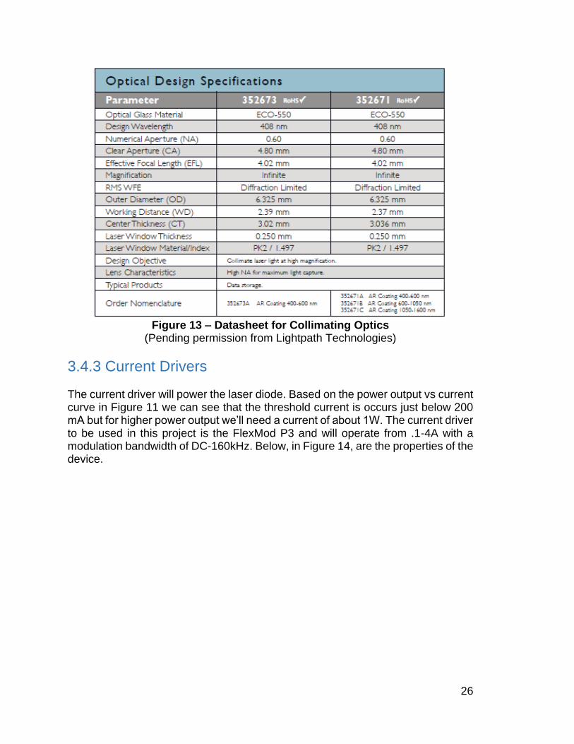
Figure 13 – Datasheet for Collimating Optics ..................................................... 26
Figure 14 – FlexMod P3 Device Properties ........................................................ 27
Figure 15 – FDA Laser Classifications. .............................................................. 29
Figure 16 – Specifications for Laser Safety Goggles.......................................... 30
Figure 17 – Pixy Object Detection ...................................................................... 32
Figure 18 – Pixy Back View ................................................................................ 33
Figure 19 – Edge Detection Example ................................................................. 34
Figure 20 – Sobel Operator ................................................................................ 35
Figure 21 – Motion Detection Example .............................................................. 36
Figure 22 – Variable Reluctance Stepper Motor ................................................ 43
Figure 23 – Closed Loop Servo System with Feedback to Microcontroller ........ 43
Figure 24 – General Hardware Diagram ............................................................ 47
Figure 25 – Primary Software Architecture ......................................................... 48
Figure 26 – Cartesian and Spherical Coordinate Frame Relationship ............... 52
Figure 27 – Block Diagram of Directed Energy System ..................................... 53
Figure 28 – Web Server Software Architecture .................................................. 57
Figure 29 – CC3200 Schematic Diagram ........................................................... 63
Figure 30 – Pin Layout and Configuration for Flash Chip ................................... 64
Figure 31 – CC3200 Example Connection to Flash Chip ................................... 64
Figure 32 – Schematic of CC3200 connection to Flash Chip ............................. 65
Figure 33 – Schematic of CC3200 connection to 2.4GHz Antenna .................... 65
Figure 34 – Schematic of FT2232D Debugger Chip .......................................... 66
Figure 35 – Schematic of Power Management .................................................. 66
Figure 36 – PCB Layout ..................................................................................... 67
Figure 37 – Power Supply Schematic ................................................................ 70
Figure 38 – Power Supply Board Layout ............................................................ 71
Figure 39 – Finite Difference Model in One Dimension ...................................... 79
Figure 40 – Schematic of the Laser Housing with the Diode Mesh .................... 82
Figure 41 – Thermal Simulation of Polycarbonate Thermoplastic Housing ........ 82
Figure 42 – Thermal Simulation of Aluminum Housing ...................................... 83
Figure 43 – Placement of Pixy ........................................................................... 84
Figure 44 – Housing for AIR-STRIKE ................................................................. 85

vii
Figure 45 – Schematic of the Gimbal and Laser Assembly ................................ 86
Figure 46 – Final Concept Design of AIR-STRIKE ............................................. 86
Figure 47 – Final Casing .................................................................................... 89
Figure 48 – MATLAB plot of standard Gaussian function ................................... 95
Figure 49 – Three Low Order Beam Profiles ...................................................... 96
Figure 50 – A diagram of laser beam divergence ............................................... 96
Figure 51 – Diagram of optical setup to measure Power vs. Current curve ........ 97
Figure 52 – Example of Successful Ping .......................................................... 105
Figure 53 – Visualization of Labor Division ....................................................... 121
Figure 54 – Budget Distribution ........................................................................ 123
viii
List of Tables Table 1 - Relevant Raspberry Pi Model B+ Specs ............................................. 12
Table 2 – Relevant MSP430 – EXP430G2 Specifications .................................. 15
Table 3 – Relevant Tiva C-TM4C1294NCPDT Specifications ............................ 15
Table 4 – Relevant CC3200 Specifications ........................................................ 16
Table 5 – Comparison of System Processors on Relevant Specifications ......... 18
Table 6 – Wireless Communication Comparison ............................................... 39
Table 7 – Wi-Fi Options Comparison ................................................................. 40
Table 8 – Bluetooth Options Comparison ........................................................... 40
Table 9 – Wireless USB Options Comparison .................................................... 41
Table 10 – ZigBee Component Comparisons .................................................... 41
Table 11 – Required Voltage for Components ................................................... 44
Table 12 – Functions and Structures for Target Acquisition ............................... 50
Table 13 – Functions for Turret Movement ........................................................ 50
Table 14 – Functions for Fire Control ................................................................. 50
Table 15 – Functions for External Communication ............................................. 51
Table 16 – PCB Price Comparison .................................................................... 68
Table 17 – CC3200 Specifications ..................................................................... 69
Table 18 – PCB Bill of Materials ......................................................................... 75
Table 19 – Properties of Polycarbonate ............................................................. 79
Table 20 – Properties of Copper as given by Comsol’s material library ............. 81
Table 21 – Data sheet comparing the different Nylon 12 based compounds ..... 88
Table 22 – Fall 2014 Schedule ......................................................................... 120
Table 23 – Spring 2015 Schedule .................................................................... 122
Table 24 – Budget ............................................................................................ 123

1
1.0 Executive Summary Directed energy systems have long been fantasized as the staple of futuristic combat. Devices which fire promptly, with devastating beams of energy, and require no physical ammo are extremely desirable facets in any defensive system. However, despite its presence within, this technology is not confined to the realm of Science Fiction. Consistent and continuous improvement of these systems, alongside decreasing costs drives the industry forward as companies once more start investigations into the matter. In these investigations laser weaponry has already been shown capable of neutralizing unmanned aerial vehicles (UAVs) and can even force detonation of improvised explosive devices (IEDs) from a safe distance. [1] In concert with this is the push for automation. With the advent of drone systems, it is becoming clear that future weaponry will require less human input. The idea here is, of course, remove human error from the equation in order to ensure more reliable and precise results. Furthermore, it removes the danger of lost lives should the system be targeted by a return attack. The rise in these systems is evident in modern warfare, especially seen in anti-terrorism missions by the USA and allies. [2] Another driving force in warfare is the desire to prepare ourselves to defend against missile attacks from across the globe. Modern ballistics can readily travel the world from any location within minutes, resulting in significant devastation. Many ideas have been proposed to deal with such threats. A popular tactic is to simply shoot them down or force a detonation via collision at a location far from population centers or other valuable targets. In essence, we launch missiles at incoming missiles. The idea behind our project then, is to combine these various tactics into one. While it is not a novel idea, it is one that still needs refinement. The proposal is to design a miniature automatic anti-air turret which utilizes directed energy as its primary weapon. The final product, AIR-STRIKE, will automatically detect, track, and burst balloons of a specified color utilizing a high powered laser mounted upon its head. Furthermore, we aim to contain it all within a space efficient system that does not rely on external hardware for its processing. AIR-STRIKE will leverage image processing techniques in its identification and tracking of potential targets. We aim to choose the most processing-efficient methods in order to offset the disadvantage of working without external hardware such as a laptop or desktop computer. Microcontrollers are often limited on their capabilities and as such it is vital that processing not be wasted or else the machine will function too slowly to be effective. Movement of the laser will be handled by a gimbal system, which will be controlled by the primary microcontroller. The gimbal system will have pan and tilt

2
mechanisms in order to provide azimuthal and elevational movement freedoms, enabling us to aim at and fire upon a designated target. After a detection the system will track and fire upon a target until it has been neutralized or leaves the field of view. Safety mechanisms will be set in place, such as limitations on the gimbal, such that the laser will be unable to harm persons in the vicinity. This document, then, is a culmination of our research, design, and proposed methods of testing for the AIR-STRIKE system. The first major segment, the research, will detail our various options for different components and techniques and our analysis of them. The design portion will cover our selection of parts, and the manner by which we will incorporate them in the overall design. The final segment will focus upon the methodologies we intend to use to test our product. In its entirety, AIR-STRIKE serves to test our capabilities and provide proof of the prospects of the implemented technologies.
3
2.0 Project Description
2.1 Project Motivation and Goals The primary motivation for this project is an interest in the technology at play. Directed energy systems are a topic of fascination for our group members, and as such we are quite enamored by the prospect of designing a system that will involve their usage. Image processing is another topic of interest, though on a more practical level. Technology to retrieve information from visual input is a hot topic in today’s world, as we push systems to act in a more intelligent manner similar to how a human would upon viewing a scene. This is seen particularly in drones and self-driving cars. Together these technologies are relevant and important to our respective fields and interests. Secondary motivation lies in preparing ourselves for the industry at large. As graduation is on the horizon for each member of our team, we seek to improve our skills in order to improve our career prospects. As both optics and system automation our important technologies in the current industry, it is important that we familiarize ourselves with them in order to ensure that we can attain employment that is both satisfying and revolutionary in our fields. In concert with this is an innate desire to test our perceived limits. This project carries the added goal of pushing ourselves in such a manner that we hope to identify our personal weaknesses in strengths. This information will allow us to improve our understandings of ourselves as well as enable us to better our performance. The choice in this particular project has the added benefit of leveraging each of our individual skillsets. As our group is composed of a photonics engineer, an electrical engineer, and two computer engineers, we wanted to complete a design which necessitated each of us to contribute our unique learnings. We are pleased then, to note that our project contains purpose for each of our team members. The project contains an optical system, the directed energy system, for our photonics engineer. The design of a PCB and the management of our system’s processors, line traces, and various other components fit the capabilities of our electrical engineer. Finally, the software challenges faced and their interfacing with the hardware selected are tasks suited to our computer engineers. It is our belief thusly, that this project will provide us each with significant technical experience.
2.2 Objectives
Our objective in the creation of AIR-STRIKE is to provide a miniature realization of an automatic anti-air defense system that uses directed energy to neutralize its targets. In this we aim to ensure reliability, precision, and safety. We define reliability as the success rate of neutralizing a target. To be reliable AIR-STRIKE must consistently target and pop balloons. We define precision as the accuracy of our direct energy weapon system. To be accurate the system needs to always fire

4
a beam at a designated target as opposed to missing. We define safety in terms of the likelihood of harm coming to user or person in the area. To be safe this likelihood must be near zero. These three aspects are interlocked on a fundamental level in that each impacts that other.
Another significant objective is to perform all computation without relying on an external computer. Image processing is usually a fairly expensive process and as such it requires dedicated resources or a sufficiently powerful processor. We aim to accomplish this by having dedicated image processing hardware, as opposed to performing the processing upon our microcontroller. Instead this hardware, the PixyCam, will send the target coordinates to the microcontroller after performing the processing on its own. This frees up our processing time for handling control of the laser and translating coordinates.
2.3 Project Requirements and Specifications After our initial research, the team decided on a set of functional requirements in order to ascertain the completeness of our project by. These align with our previously stated goals and objectives, as we aim to design a capable system. While we wish to exceed each of these limitations if possible, they serve as a baseline for us to work towards. In the following sub-sections we will provide a general discussion for of the various systems requirements.
The detection rate of a target in the field of view shall be at least 70%
The system shall be capable of tracking a single target
The system shall be able to neutralize a target within ten feet
Upon detection, time to first kill shall be 7 seconds
The total field of view shall be 120° with two cameras
The directed energy system shall deliver at least 100 mW of power in a
concentrated beam
The wavelength of the beam shall be in the visible light spectrum
The mounted laser should be capable of movement 120° azimuthal (60°
each direction) and 120° elevational (60° each direction)
The system will be capable of modulating the power delivered by the
directed energy system
The system shall attain 100% accuracy on kill-shots for safety purposes
The cameras shall capture frames at a minimum of 15 frames per second
The system shall be able to operate autonomously
The system shall be interfaceable through USB or wireless signals by
external devices
External devices will be able to close the laser shutters
The system shall contain hardware to force the laser off for safety
purposes
5
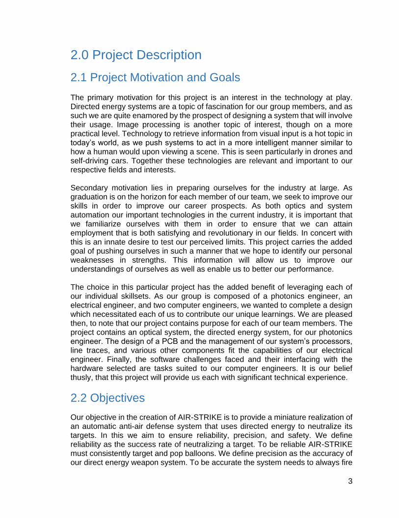
2.3.1 Microcontroller Requirements The microcontroller is responsible for image information from the camera system, taking inputs from an external user interface, and outputting signals to the motor, external interface, and laser systems to create an expected behavior. Figure 1 shows the inputs and outputs of the microcontroller.
Figure 1 – Inputs and Outputs for the Microcontroller
2.3.1.1 Handling Input from Cameras The cameras will send images to the microcontroller where image processing and target acquisition will occur. However it is likely the target will be moving and the directed energy beam is most effective when focused on the same spot. This creates a time constraint from receiving the image to target identification. Therefore the microcontroller used must be able to process an image and output the necessary information to the motor and laser systems at least 10 times per second. Specifications wise that means the MCU will need a clock speed of at least 60MHz. This is made more challenging by the fact that image processing can be computationally expensive. Finally since the microcontroller is doing the image processing, it will need enough memory to store the image some processed form of it. Because of that the microcontroller should have at least 1MB of primary memory, but having a 16MB of secondary memory would be preferable.
Microcontroller
Camera
Motor Directed Energy
External Interface
External Interface
Image
User Input
Rotation Laser Driver
Status Data
Inputs
Outputs

6
2.3.1.2 Output to Motors
After target acquisition the microcontroller will calculate how much the motors need to rotate by in order to place the target in the line of fire. It will need to transmit these values digitally to two motors (one for the yaw and another for the pitch) that control the orientation of the directed energy system. A possible stretch specification would be to account for speed at which the motors rotate and how fast an object is moving so the line of fire can placed where the target is predicted to be instead of where it was. Since servo motors are being used and are controlled with pulse width modulation (PWM) the microcontroller will need to have at least two PWM outputs.
2.3.1.3 Output to Directed Energy System Safety is of the utmost importance when operating this system so the output to turn on the directed energy system should only be sent when the target is in the line of fire. The microcontroller will need to check if the user has enabled the system to fire and if the directed energy will hit the target. If these conditions are satisfied then a digital output will be sent to possibly a digital potentiometer to adjust the current running though the directed energy system. A reason for the digital output to control the level of current rather than an on/off state is so that during testing we can still see the effects of the directed energy system without it being at dangerous levels. Having a variable current level would also allow the directed energy system to be switched out with other devices that can be driven with a current driver easily.
2.3.1.4 External Interface Capabilities The external interface will be how the microcontroller receives and sends information to the user. It is unique in that it is the only system that will have duplex communication with the microcontroller. The microcontroller will need to send status information to the interface such as: target acquisition status, visual feed (from the camera), directed energy state, and orientation. It will also need to read messages from the external interface to take certain actions or modify values. For example the amount of current going through the directed energy system is controlled by the microcontroller which should be modifiable through the external interface. Other values that should be modifiable in the microcontroller include the orientation of the directed energy system and of course some form of safety switch such that the directed energy system cannot be turned on without the safety being off. Another aspect of the external interface is that it is implemented through a wired and wireless medium. Considering this the microcontroller will need to be able to communicate through USB and Bluetooth.
2.3.2 Image Capture Subsystem An image capture subsystem generally needs to deliver frames to the rest of the system. However, after research we have chosen to utilize Pixy cameras from

7
Charmed Labs. This changes the primary purpose of the subsystem as these cameras perform object detection and tracking within their own hardware. For this reason this subsystem’s primary objective is to supply target coordinates to the primary microcontroller in order to direct the mounted laser for neutralization. However, for the purposes of user friendliness, we also intend to have it deliver images so that they can be viewed by the user on external devices interfacing with the project. The reason for our choice in field of view is primarily to limit the location of our targets to one side of the turret. This is a safety precaution so that the device does not try to fire behind itself where a view may be attempting to observe the project in action. Furthermore, we believe that this field of view is more than enough to demonstrate the capabilities, and that to increase the field of view would be possible should that be the goal. Our frame rate choice is based on our understanding of image processing. The Pixy cameras claim an output of 50 frames per second, but in the case of another camera, we imagine we would be far more limited, due to processing being done on the main microcontroller. In case this happens, we decided to keep our conservative requirement. Finally, we chose our target detection rate at 70% because we determined that this is a fair value for determining the capabilities of the design. While this percentage is ultimately determined by the Pixy camera, we expect that it should more than meet this and include this value only in the case that we would need to implement our own detection algorithms. In such a case we would need to refine the software to this point. Another reason for this percentage is because guaranteeing higher detection may also increase the number of false detections and with a powerful laser, false detections are far more dangerous and need to be avoided. As such, we would prefer a target go unnoticed than a non-target be lazed.
2.3.2 Directed Energy Subsystem The Direct Energy subsystem is a somewhat complex system with multiple necessary capabilities. Foremost, a system needs to be in place to force the system to close its shutter. This is mostly a safety precaution as a laser that meets our requirement wattage will be considered a Class IV laser and thus is hazardous if it contacts human skin, or worse human eyes. It is for a similar reason that we limited the gimbal requirements to only 120° azimuthal and 120° elevational. This allows the subsystem to only aim on one side of the device, protecting the device itself from the laser as well as users on the opposite side. The reason we chose the visible light spectrum for our laser is because these wavelengths are the most commonly absorbed. As such a beam of these wavelengths is far more damaging to our intended targets as the target will absorb more of the delivered power until it heats up to the point of neutralization.
8
Furthermore, lasers of these wavelengths have been shown before to be capable of bursting a balloon and as such we know that our laser will be capable of its intended task.
2.3.3 System Controller Software The software that runs on our primary microcontroller needs to be able to manage all the components involved in the entire system. Aptly, this can be labeled as the System Controller. This software needs primarily to be able to manage the multitude of different messages received and sent to the various components, while also performing processing in order to properly convey the intent of these messages. In order to do this the system needs to incorporate a series of functions for receiving and transmitting data. Upon receiving a message, the port will be used to determine where the message comes from (e.g. the camera). From here the message can be sent to a specified function intended to process said message. A primary concern for this system is that it needs software capabilities to properly convert the coordinates of targets in the camera’s view to angles the servo controller can utilize to aim the laser. These conversions need to be precise so as to maintain our 100% accuracy requirement. The reason for such a requirement is, as emphasized frequently so far, safety. We do not wish for a miss that could cause harm to persons in the vicinity.
2.3.4 External Interfacing Software While not necessary for normal operation, we wish to extend options of communicating with the device to enable the user to access various options from a multitude of platforms. To do this we must create a messaging format to communicate with the primary system controller that can be easily implemented across a multitude of communication methods. External devices need to be able to access a multitude of options. Chief among these is the ability to enable and disable the ability for the system to activate its laser. Other features hoped for, but not required (mostly due to time and personnel constraints) are capabilities such as designating a target, manually directing the laser, and manually adjusting the power modulation. For instance, a user could manually aim a target not trained for by the system and then slowly increase the power provided by the directed energy system until neutralization occurs. Then they could quickly force the shutter closed.
9
3.0 Research Before designing our targeting system, extensive research was required in order to make the correct decisions on parts and theories. The research consisted mostly of using search engines to learn about various concepts ranging from networking, tracking algorithms and how to gimbalize motors. Researching and reading through datasheets was another integral part of our researching process. Datasheets are the building blocks that we need in order to know how to power and integrate all of our subsystems together.
3.1 Existing Related Projects While previous Senior Design groups have designed targeting systems, that also include a laser, ours has a few unique requirements to it. Previous senior design groups’ targeting systems would track a designated object, but ours will not only autonomously track the target, but also pop the balloon rather than simply keep a weak laser pointed on it. Our system also, to our knowledge, is the only system to incorporate a variable power output for the laser to help conserve energy. The laser will only fire the minimum needed wattage at the balloon to pop it, depending on the distance from the laser and the color of the balloon. Furthermore, we intend to localize the computations to our project, without relying on an external device for our computations.
3.2 Relevant Technologies While our system is not a practical solution to a real targeting system, it does resemble targeting systems sold in the real world. Defense contractors and subcontractors design and build targeting systems to sell to both domestic and foreign armed forces. Their targeting systems can either be incorporated on aircrafts, ships, vehicles or stationary to the ground. Targeting systems are versatile systems that range from air-air, air-to-surface, surface-to-air or surface-to-surface targeting.
3.2.1 Optical Targeting Systems Certain targeting systems are mechanical based while other are more optical based. While our system does not have several different optical devices involved in the tracking process, our system can be included in the optical targeting system department due to the cameras and laser that we use. For real world optical targeting systems, typically several optical subsystems are required in order to generate accurate targeting results. Since our system is a very basic example of an optical targeting system, we plan on only having one optical subsystem.

10
3.2.1.1 Lockheed Martin JSF EOTS Chris, Andrew and Scott have all interned and worked at Lockheed Martin Missiles and Fire Control. Due to this commonality, we unsurprisingly wanted to design a targeting system of our own. Both Andrew and Scott have worked on the Joint Strike Fighter Electro Optical Targeting System in the past. The JSF EOTS is the air-to-air and air-to-surface targeting system incorporated on the new F-35 fighter jet (also built by Lockheed Martin). Due to trade secrets, and classified material, the details of the JSF EOTS cannot be incorporated in this document. The previous knowledge gained, from working on the JSF EOTS, will help our group understand how to design, but more importantly, how to integrate our design components together.
3.2.1.2 Raytheon MTS Raytheon, another defense contractor, also develops their own optical targeting system called the Multi-Spectral Targeting System (MTS). The MTS is a more versatile system that is incorporated on several different aircrafts, both planes and helicopters. It is clear that American defense contractors, as well as their customers, are intrigued with optical targeting systems and see the development of them as a critical part of our armed forces success.
3.2.2 Anti-Air Weaponry Both of the targeting systems listed above, along with several others, are a part of a unique group of products that are anti-air weapons. Any system that targets and/or destroys systems in the air falls under this category. Our system will be targeting balloons classifying it as an anti-air weapon. Anti-air weapons are critical to our nation’s defense due to incoming missiles and foreign aircrafts. Anti-air weapons allow our nation, and any other nation, to continue to succeed in defending its citizens and keeping them safe.
3.2.3 Object Detection Systems Object detection systems are another form of defense system that autonomously detects dangerous systems and either shoots them down or sends a signal to another system to shoot it down. While balloons pose no threat to the American government or armed forces, the concept of our system can be utilized for real world applications. Rather than searching and detecting balloons, a real world system can search and target aircrafts or missiles to help support our armed forces. There are several anti-air weapons that target and shoot down missiles that have helped saved thousands of lives. Lockheed Martin and Raytheon both have their own anti-missile systems that our government, and ally governments purchase.
11
3.3 System Processing The system processor is responsible for processing inputs from the camera and external interface and outputting data to the motor, laser, and external interface systems. There are several main requirements that the processor will have to satisfy which includes processing an image to acquire a target, moving the line of fire within a time constraint, enabling the directed energy system, and storing images so they can be sent to the external interface. These requirements point to the need for a relatively large amount of memory to store information and the ability to process data in a timely manner. This issue is further compounded by the fact that image processing and object identification can be computationally expensive.
3.3.1 Single-Board Computers Single-board computers are great for their general purpose design and in a project where image processing, external networking, and digital outputs are needed. One such single-board computer under consideration is the Raspberry Pi which is well known as a cheap and flexible processing board for hobbyists. The Raspberry Pi uses a 700MHz ARM processor and has 512 MB of SDRAM (on the Model B and above) so it definitely has enough memory to store images from the camera. It also has a Graphical Processing Unit (GPU) which could aid with image processing. Given its design as a general purpose computer, adding in functionality such as object detection or network interfaces is as easy as downloading the supporting library. For example, a popular image processing library named OpenCV could be downloaded onto the Raspberry Pi and utilized in the software which would save time on implementing image processing algorithms. The Raspberry Pi also comes with several USB ports that would aid with the external interface especially since a WiFi device could be used with those ports and as with image processing, libraries already exist that facilitate network communication. It comes with numerous digital outputs and probably the biggest advantage is that the high level Python programming language is used. Digital outputs can be easily controlled by GPIO Python library. However the general purpose advantage of the Raspberry Pi is also its major disadvantage because it runs an operating system. This means many real time operations are not possible and the operating system itself takes up system resources. So while the specifications of the Raspberry Pi are impressive for the $35 price, not all of those resources would be available as they would be in use by other processes. From experimentation performing edge detection at the 320x240 resolution on yielded around 10 frames per second. This may be too slow to smoothly track a moving target. Finally the system may need to use multiple cameras to provide a wider field of view, but the board only has one camera interface. To use multiple cameras there would need to be multiple daughter boards to select between the cameras.

12
Of the four models of the Raspberry Pi only the Model B+, specs shown in Table 1, and compute module would be suitable. Model A only has half the SDRAM of the Model B and if the project plans for two servo motors then it will require two GPIO pins capable of pulse width modulation. Unfortunately the Model A only has one pin capable of hardware pulse width modulation. The other pins can do software pulse width modulation, but due to Raspberry Pi not being a real time system, the pulse widths can be inaccurate and cause jitter in the motors. A solution to this would be to use a servo driver which has its own clock and can guarantee an accurate pulse width. The Model B has double the memory, but it still suffers from having only one hardware PWM GPIO. The Model B+ introduces additional pins capable of hardware PWM so there would be no need to implement a servo driver. The final model is the compute module development kit. It contains additional IO pins, ports, 4GB flash memory chip and was designed for implementation on a PCB. While the compute module offers even greater flexibility in the use of inputs and outputs its cost is more than 6 times the Model B+ if the Raspberry Pi were to be used then this model would most likely only be used for the prototype and final product while development would occur on the Model B+.
Table 1 - Relevant Raspberry Pi Model B+ Specs
CPU 700 MHz ARM11
GPU Broadcom VideoCore 4, 250 MHz
Memory 512 MB
Network Ports
10/100 Mbit/s Ethernet port or through USB adapter
Power Source
Through the MicroUSB or GPIO (5V)
Video Inputs
Only 1 Camera Serial Interface (CSI) connector
Digital I/O Pins
40 GPIO pins (4 for PWM)
USB ports 4 USB 2.0 ports
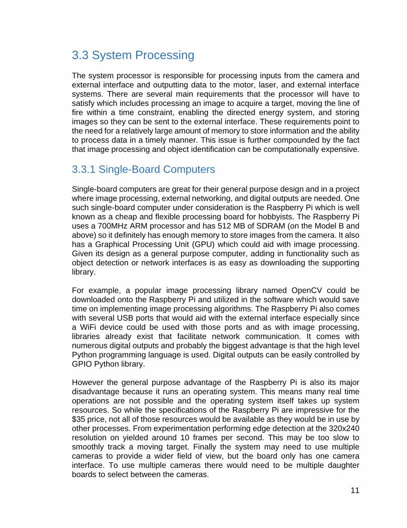
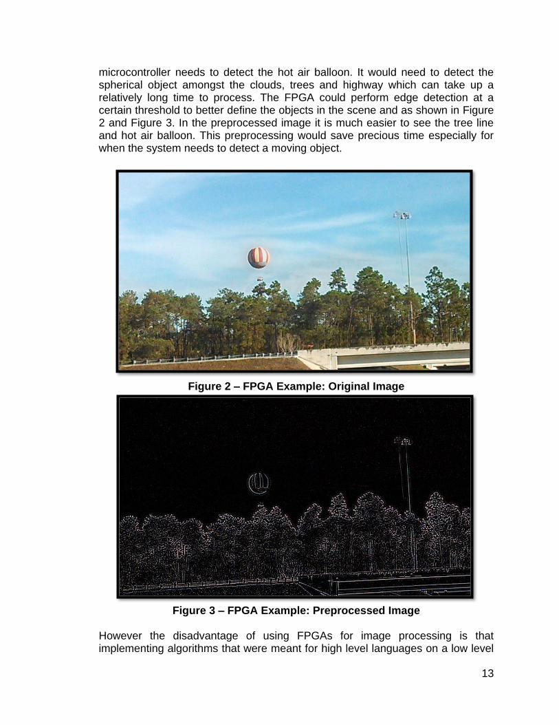
3.3.2 Field-Programmable Gate Array (FPGA) Image processing can be very intensive on the processor and in time constrained system that can greatly impact performance. As stated previously, the Raspberry Pi only processed images at 10 frames per second which is slow when tracking a fast moving object. So it was decided that an FPGA could be used in conjunction with a microcontroller or single-board computer to perform some quick pre-image processing so that there will be less work on main processor. The advantage of using an FPGA is that it is very fast compared to the image processing speed of a microcontroller. This is because in conventional software the image is usually processed in a serial stream a block at a time while FPGAs can process an image in parallel. The figures below show how this could work. Suppose the
13
microcontroller needs to detect the hot air balloon. It would need to detect the spherical object amongst the clouds, trees and highway which can take up a relatively long time to process. The FPGA could perform edge detection at a certain threshold to better define the objects in the scene and as shown in Figure 2 and Figure 3. In the preprocessed image it is much easier to see the tree line and hot air balloon. This preprocessing would save precious time especially for when the system needs to detect a moving object.
Figure 2 – FPGA Example: Original Image
Figure 3 – FPGA Example: Preprocessed Image
However the disadvantage of using FPGAs for image processing is that implementing algorithms that were meant for high level languages on a low level
14
interface is complex and time consuming. For these reasons FPGAs would only be used in this project if there was sufficient time and if the other alternatives did not have satisfactory performance.
3.3.3 Microcontroller A microcontroller is capable of being a real time system which is important in a time constrained system. There are a wide variety of microcontrollers each designed around specific needs. Unlike the single-board computers, microcontrollers can be used without an operating system so not as many computer resources are taken up. For this project the microcontroller will need at least one SPI to communicate with the camera, two PWM for the two servos, a digital output for the laser driver and finally a way to communicate wirelessly. However there is still the issue of image processing and target acquisition being computationally intensive. As previously discussed one alternative is to perform image pre-processing on an FPGA, but that introduces a very complex system. Another alternative the team discussed is offloading the image processing to other microcontrollers, specifically the CMUcam5 also known as Pixy. The Pixy is able to perform image processing and identify targets at a speedy 50 frames per second. It then can transmit just the target coordinates to the main microcontroller for quick processing. It is likely that the last alternative will be used as it is the simplest and easy to implement and given this assumption three microcontrollers were considered for this project: MSP430-EXP430G2, Tiva C TM4C1294NCPDT, and the CC3200. The first microcontroller under consideration was the MSP430. The advantage of the MSP430 is that every team member has one and is familiar with its programming language. It’s also very lightweight and uses a small amount of power which can be a benefit if the system was battery powered. It meets the requirements by having 2 SPI, PWM and several GPIO. The need for a wireless interface can be satisfied by using the SimpleLink Wi-Fi booster pack which uses the CC3100 chip. However the MSP430 was focused around “Ultra-low” power usage and because of that the processing power suffers.
From Table 2Table 1 the processor only has a clock speed of 16MHz which is not fast enough to process an image in a timely manner, but since most of the image processing will be done on a separate microcontroller this is not as big issue as with the lack of a wireless interface which can be remedied with the SimpleLink Wi-Fi addition. The main issue is the lack of memory that can be used. While it has plenty of room for code, one of the stretch goals of this project is to stream video through an external interface and the amount of memory would be inadequate for this purpose. Also since the Pixy was designed only to detect objects and not record video, storing images on the Pixy is not an option.
15
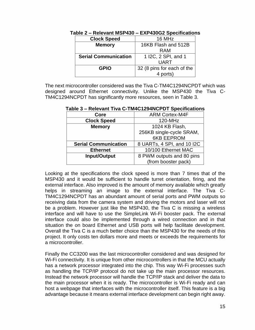
Table 2 – Relevant MSP430 – EXP430G2 Specifications
Clock Speed 16 MHz
Memory 16KB Flash and 512B RAM
Serial Communication 1 I2C, 2 SPI, and 1 UART
GPIO 32 (8 pins for each of the 4 ports)
The next microcontroller considered was the Tiva C-TM4C1294NCPDT which was designed around Ethernet connectivity. Unlike the MSP430 the Tiva C-TM4C1294NCPDT has significantly more resources, seen in Table 3.
Table 3 – Relevant Tiva C-TM4C1294NCPDT Specifications
Core ARM Cortex-M4F
Clock Speed 120-MHz
Memory 1024 KB Flash, 256KB single-cycle SRAM,
6KB EEPROM
Serial Communication 8 UARTs, 4 SPI, and 10 I2C
Ethernet 10/100 Ethernet MAC
Input/Output 8 PWM outputs and 80 pins (from booster pack)
Looking at the specifications the clock speed is more than 7 times that of the MSP430 and it would be sufficient to handle turret orientation, firing, and the external interface. Also improved is the amount of memory available which greatly helps in streaming an image to the external interface. The Tiva C-TM4C1294NCPDT has an abundant amount of serial ports and PWM outputs so receiving data from the camera system and driving the motors and laser will not be a problem. However just like the MSP430, the Tiva C is missing a wireless interface and will have to use the SimpleLink Wi-Fi booster pack. The external interface could also be implemented through a wired connection and in that situation the on board Ethernet and USB ports will help facilitate development. Overall the Tiva C is a much better choice than the MSP430 for the needs of this project. It only costs ten dollars more and meets or exceeds the requirements for a microcontroller. Finally the CC3200 was the last microcontroller considered and was designed for Wi-Fi connectivity. It is unique from other microcontrollers in that the MCU actually has a network processor integrated into the chip. This way Wi-Fi processes such as handling the TCP/IP protocol do not take up the main processor resources. Instead the network processor will handle the TCP/IP stack and deliver the data to the main processor when it is ready. The microcontroller is Wi-Fi ready and can host a webpage that interfaces with the microcontroller itself. This feature is a big advantage because it means external interface development can begin right away.
16
Also when the PCB is being made, the team won’t have to worry about connecting a network processor because only an U.FL antenna would need to be connected. Table 4 shows the relevant specifications for this microcontroller.
Table 4 – Relevant CC3200 Specifications
Core ARM Cortex M4
Clock Speed 80MHz
Memory 256KB
Serial Communication 2 UARTs, 1 SPI, and 1 I2C
Input/Output 4 PWM and 27 GPIO
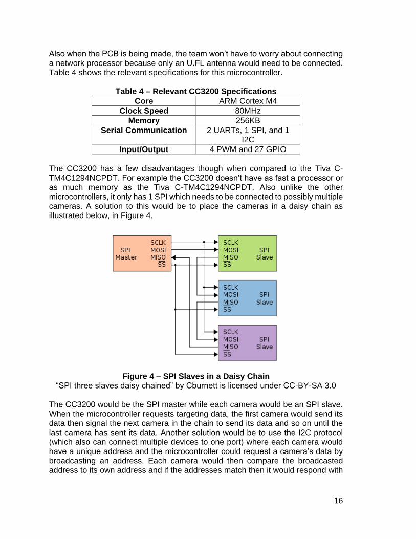
The CC3200 has a few disadvantages though when compared to the Tiva C- TM4C1294NCPDT. For example the CC3200 doesn’t have as fast a processor or as much memory as the Tiva C-TM4C1294NCPDT. Also unlike the other microcontrollers, it only has 1 SPI which needs to be connected to possibly multiple cameras. A solution to this would be to place the cameras in a daisy chain as illustrated below, in Figure 4.
Figure 4 – SPI Slaves in a Daisy Chain
“SPI three slaves daisy chained” by Cburnett is licensed under CC-BY-SA 3.0
The CC3200 would be the SPI master while each camera would be an SPI slave. When the microcontroller requests targeting data, the first camera would send its data then signal the next camera in the chain to send its data and so on until the last camera has sent its data. Another solution would be to use the I2C protocol (which also can connect multiple devices to one port) where each camera would have a unique address and the microcontroller could request a camera’s data by broadcasting an address. Each camera would then compare the broadcasted address to its own address and if the addresses match then it would respond with

17
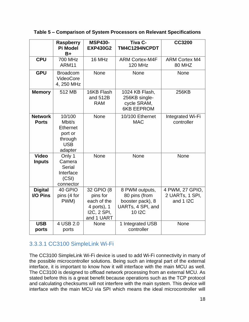
data. The disadvantage of this method is that there is overhead when setting up the data request and is much more complex than SPI. After researching the three options for microcontrollers, the main contenders were the CC3200 and the Tiva C- TM4C1294NCPDT. The MSP430 was dropped because the other two microcontrollers had superior specifications. The advantage of the CC3200 is that it has an integrated network processor, but unfortunately it has limited serial communication ports. On the other hand the advantage of the Tiva C is that it has plenty of communication ports, but would need an 802.11 implementation for Wi-Fi communication. A comparison of our choices is shown below in Table 5.
18
Table 5 – Comparison of System Processors on Relevant Specifications
3.3.3.1 CC3100 SimpleLink Wi-Fi The CC3100 SimpleLink Wi-Fi device is used to add Wi-Fi connectivity in many of the possible microcontroller solutions. Being such an integral part of the external interface, it is important to know how it will interface with the main MCU as well. The CC3100 is designed to offload network processing from an external MCU. As stated before this is a great benefit because operations such as the TCP protocol and calculating checksums will not interfere with the main system. This device will interface with the main MCU via SPI which means the ideal microcontroller will
Raspberry Pi Model
B+
MSP430-EXP430G2
Tiva C-TM4C1294NCPDT
CC3200
CPU 700 MHz ARM11
16 MHz ARM Cortex-M4F 120 MHz
ARM Cortex M4 80 MHZ
GPU Broadcom VideoCore 4, 250 MHz
None None None
Memory 512 MB 16KB Flash and 512B
RAM
1024 KB Flash, 256KB single-cycle SRAM,
6KB EEPROM
256KB
Network Ports
10/100 Mbit/s
Ethernet port or through
USB adapter
None 10/100 Ethernet MAC
Integrated Wi-Fi controller
Video Inputs
Only 1 Camera Serial
Interface (CSI)
connector
None None None
Digital I/O Pins
40 GPIO pins (4 for
PWM)
32 GPIO (8 pins for
each of the 4 ports), 1 I2C, 2 SPI,
and 1 UART
8 PWM outputs, 80 pins (from
booster pack), 8 UARTs, 4 SPI, and
10 I2C
4 PWM, 27 GPIO, 2 UARTs, 1 SPI,
and 1 I2C
USB ports
4 USB 2.0 ports
None 1 Integrated USB controller
None
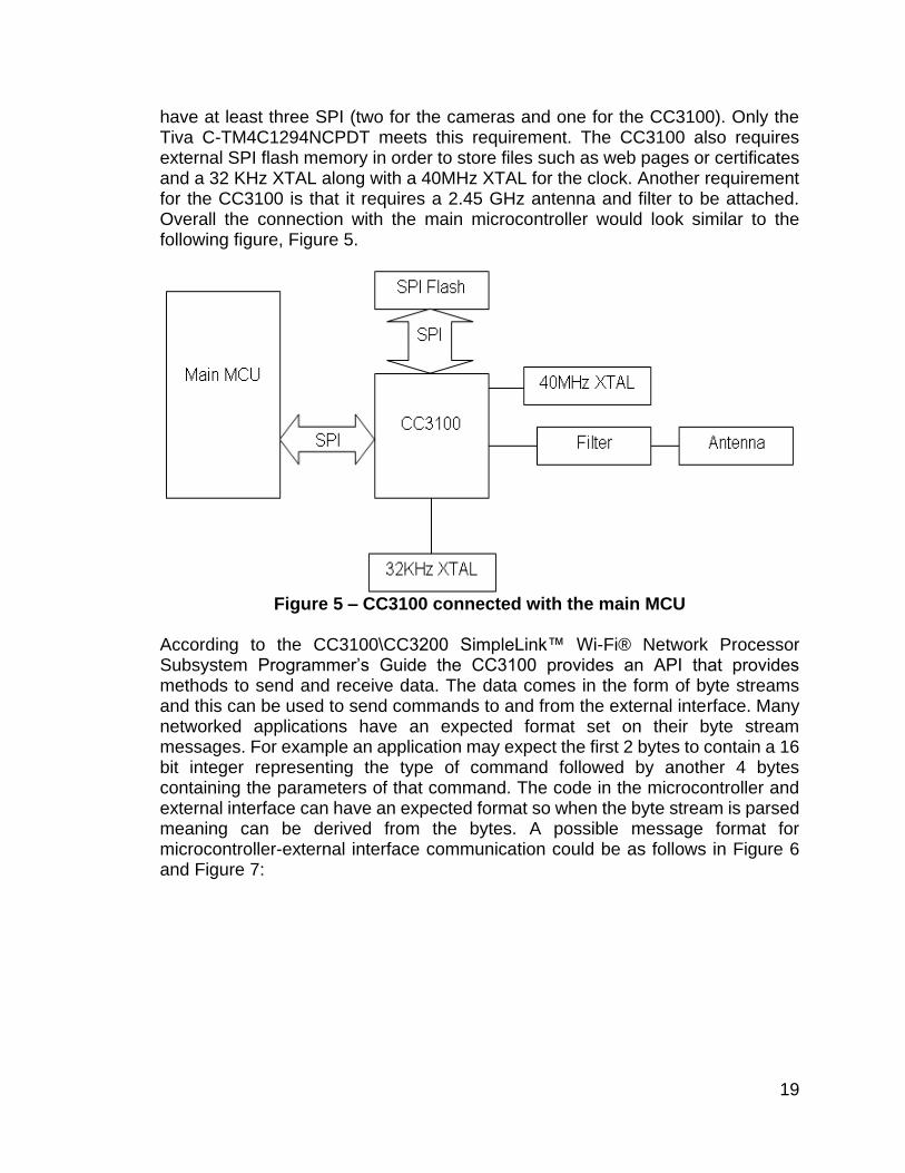
19
have at least three SPI (two for the cameras and one for the CC3100). Only the Tiva C-TM4C1294NCPDT meets this requirement. The CC3100 also requires external SPI flash memory in order to store files such as web pages or certificates and a 32 KHz XTAL along with a 40MHz XTAL for the clock. Another requirement for the CC3100 is that it requires a 2.45 GHz antenna and filter to be attached. Overall the connection with the main microcontroller would look similar to the following figure, Figure 5.
Figure 5 – CC3100 connected with the main MCU
According to the CC3100\CC3200 SimpleLink™ Wi-Fi® Network Processor Subsystem Programmer’s Guide the CC3100 provides an API that provides methods to send and receive data. The data comes in the form of byte streams and this can be used to send commands to and from the external interface. Many networked applications have an expected format set on their byte stream messages. For example an application may expect the first 2 bytes to contain a 16 bit integer representing the type of command followed by another 4 bytes containing the parameters of that command. The code in the microcontroller and external interface can have an expected format so when the byte stream is parsed meaning can be derived from the bytes. A possible message format for microcontroller-external interface communication could be as follows in Figure 6 and Figure 7:

20
0 32
Message Length Unsigned Short Integer
(2 Bytes)
Message Type Unsigned Short Integer
(2 Bytes)
Message Body
(Size depends on the message type)
Figure 6 – General format for all messages 0 32
Message Length Unsigned Short Integer
(2 Bytes)
Message Type Unsigned Short Integer
(2 Bytes)
Target ID Unsigned Short Integer
(2 Bytes)
Camera ID (Which camera is detecting the target)
Unsigned Short Integer (2 Bytes)
Target X Coordinate Unsigned Integer
(4 Bytes)
Target Y Coordinate Unsigned Integer
(4 Bytes)
Figure 7 – Example format for target position message
3.3.3.2 Bluetooth with the CC2560 Another possible requirement for the microcontroller is to support Bluetooth communication for the external interface. Unfortunately the CC3100 SimpleLink Wifi chip does not support Bluetooth so an additional controller will be required to provide a Bluetooth interface. The CC2560 Bluetooth and Dual-Mode Controller would be an ideal solution to this problem because it provides an integrated Bluetooth interface and similarly to the CC3100, can communicate with the main MCU via serial port. Also very convenient is that the CC2560 uses UART to communicate which is an advantage because many of the Tiva C’s SPI will probably be taken by cameras and the CC3100. If the CC2650 were to be used it would require additional components such as a 26MHz external crystal, a slow clock frequency of 32kHz and an antenna. It would connect to the microcontroller as shown in Figure 8 below.
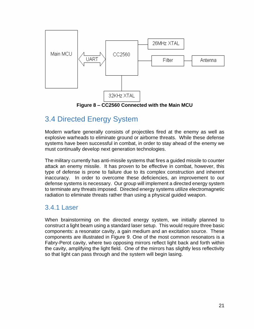
21
Figure 8 – CC2560 Connected with the Main MCU
3.4 Directed Energy System Modern warfare generally consists of projectiles fired at the enemy as well as explosive warheads to eliminate ground or airborne threats. While these defense systems have been successful in combat, in order to stay ahead of the enemy we must continually develop next generation technologies. The military currently has anti-missile systems that fires a guided missile to counter attack an enemy missile. It has proven to be effective in combat, however, this type of defense is prone to failure due to its complex construction and inherent inaccuracy. In order to overcome these deficiencies, an improvement to our defense systems is necessary. Our group will implement a directed energy system to terminate any threats imposed. Directed energy systems utilize electromagnetic radiation to eliminate threats rather than using a physical guided weapon.
3.4.1 Laser When brainstorming on the directed energy system, we initially planned to construct a light beam using a standard laser setup. This would require three basic components: a resonator cavity, a gain medium and an excitation source. These components are illustrated in Figure 9. One of the most common resonators is a Fabry-Perot cavity, where two opposing mirrors reflect light back and forth within the cavity, amplifying the light field. One of the mirrors has slightly less reflectivity so that light can pass through and the system will begin lasing.
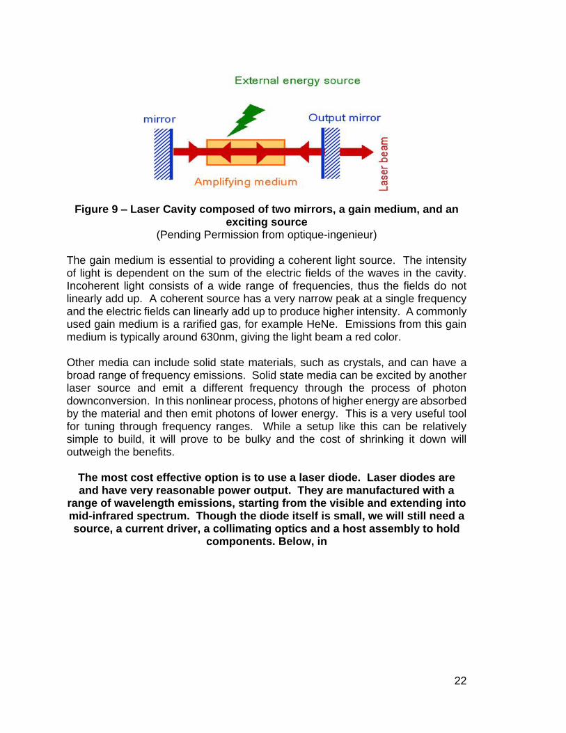
22
Figure 9 – Laser Cavity composed of two mirrors, a gain medium, and an
exciting source (Pending Permission from optique-ingenieur)
The gain medium is essential to providing a coherent light source. The intensity of light is dependent on the sum of the electric fields of the waves in the cavity. Incoherent light consists of a wide range of frequencies, thus the fields do not linearly add up. A coherent source has a very narrow peak at a single frequency and the electric fields can linearly add up to produce higher intensity. A commonly used gain medium is a rarified gas, for example HeNe. Emissions from this gain medium is typically around 630nm, giving the light beam a red color. Other media can include solid state materials, such as crystals, and can have a broad range of frequency emissions. Solid state media can be excited by another laser source and emit a different frequency through the process of photon downconversion. In this nonlinear process, photons of higher energy are absorbed by the material and then emit photons of lower energy. This is a very useful tool for tuning through frequency ranges. While a setup like this can be relatively simple to build, it will prove to be bulky and the cost of shrinking it down will outweigh the benefits.
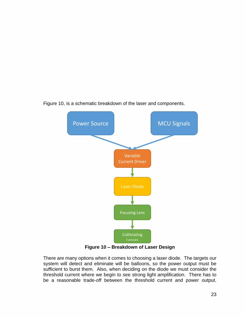
The most cost effective option is to use a laser diode. Laser diodes are and have very reasonable power output. They are manufactured with a
range of wavelength emissions, starting from the visible and extending into mid-infrared spectrum. Though the diode itself is small, we will still need a source, a current driver, a collimating optics and a host assembly to hold
components. Below, in
23
Figure 10, is a schematic breakdown of the laser and components.
Figure 10 – Breakdown of Laser Design
There are many options when it comes to choosing a laser diode. The targets our system will detect and eliminate will be balloons, so the power output must be sufficient to burst them. Also, when deciding on the diode we must consider the threshold current where we begin to see strong light amplification. There has to be a reasonable trade-off between the threshold current and power output.
Power Source MCU Signals
Variable Current Driver
Laser Diode
Focusing Lens
Collimating Lenses
24
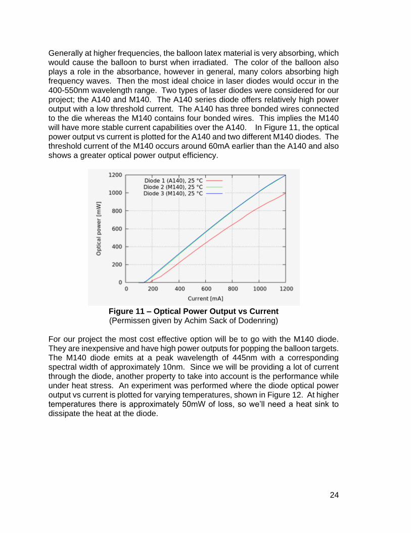
Generally at higher frequencies, the balloon latex material is very absorbing, which would cause the balloon to burst when irradiated. The color of the balloon also plays a role in the absorbance, however in general, many colors absorbing high frequency waves. Then the most ideal choice in laser diodes would occur in the 400-550nm wavelength range. Two types of laser diodes were considered for our project; the A140 and M140. The A140 series diode offers relatively high power output with a low threshold current. The A140 has three bonded wires connected to the die whereas the M140 contains four bonded wires. This implies the M140 will have more stable current capabilities over the A140. In Figure 11, the optical power output vs current is plotted for the A140 and two different M140 diodes. The threshold current of the M140 occurs around 60mA earlier than the A140 and also shows a greater optical power output efficiency.
Figure 11 – Optical Power Output vs Current (Permissen given by Achim Sack of Dodenring)
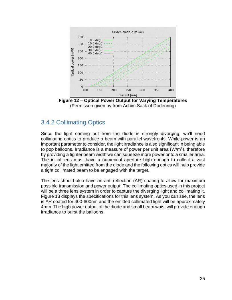
For our project the most cost effective option will be to go with the M140 diode. They are inexpensive and have high power outputs for popping the balloon targets. The M140 diode emits at a peak wavelength of 445nm with a corresponding spectral width of approximately 10nm. Since we will be providing a lot of current through the diode, another property to take into account is the performance while under heat stress. An experiment was performed where the diode optical power output vs current is plotted for varying temperatures, shown in Figure 12. At higher temperatures there is approximately 50mW of loss, so we’ll need a heat sink to dissipate the heat at the diode.
25
Figure 12 – Optical Power Output for Varying Temperatures
(Permissen given by from Achim Sack of Dodenring)
3.4.2 Collimating Optics Since the light coming out from the diode is strongly diverging, we’ll need collimating optics to produce a beam with parallel wavefronts. While power is an important parameter to consider, the light irradiance is also significant in being able to pop balloons. Irradiance is a measure of power per unit area (W/m2), therefore by providing a tighter beam width we can squeeze more power onto a smaller area. The initial lens must have a numerical aperture high enough to collect a vast majority of the light emitted from the diode and the following optics will help provide a tight collimated beam to be engaged with the target. The lens should also have an anti-reflection (AR) coating to allow for maximum possible transmission and power output. The collimating optics used in this project will be a three lens system in order to capture the diverging light and collimating it. Figure 13 displays the specifications for this lens system. As you can see, the lens is AR coated for 400-600nm and the emitted collimated light will be approximately 4mm. The high power output of the diode and small beam waist will provide enough irradiance to burst the balloons.
26
Figure 13 – Datasheet for Collimating Optics
(Pending permission from Lightpath Technologies)
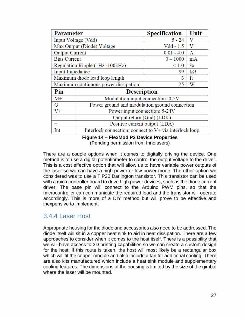
3.4.3 Current Drivers The current driver will power the laser diode. Based on the power output vs current curve in Figure 11 we can see that the threshold current is occurs just below 200 mA but for higher power output we’ll need a current of about 1W. The current driver to be used in this project is the FlexMod P3 and will operate from .1-4A with a modulation bandwidth of DC-160kHz. Below, in Figure 14, are the properties of the device.
27
Figure 14 – FlexMod P3 Device Properties
(Pending permission from Innolasers) There are a couple options when it comes to digitally driving the device. One method is to use a digital potentiometer to control the output voltage to the driver. This is a cost effective option that will allow us to have variable power outputs of the laser so we can have a high power or low power mode. The other option we considered was to use a TIP20 Darlington transistor. This transistor can be used with a microcontroller board to drive high power devices, such as the diode current driver. The base pin will connect to the Arduino PWM pins, so that the microcontroller can communicate the required load and the transistor will operate accordingly. This is more of a DIY method but will prove to be effective and inexpensive to implement.
3.4.4 Laser Host Appropriate housing for the diode and accessories also need to be addressed. The diode itself will sit in a copper heat sink to aid in heat dissipation. There are a few approaches to consider when it comes to the host itself. There is a possibility that we will have access to 3D printing capabilities so we can create a custom design for the host. If this route is taken, the host will most likely be a rectangular box which will fit the copper module and also include a fan for additional cooling. There are also kits manufactured which include a heat sink module and supplementary cooling features. The dimensions of the housing is limited by the size of the gimbal where the laser will be mounted.

28
3.4.5 Laser Safety
Since our project will incorporate a high power laser, it is critical that we take the proper safety measures to avoid any accidents that may occur with a stray laser beam. Lasers are divided into various class categories based on output power. The safest class of laser is the Class 1 category. The output from these types of lasers pose no danger to a viewer and are considered eye safe. This category includes a standard laser pointer regularly used in classrooms. There are also Class 1M lasers that if the beam was passed through magnifying optics, it may cause a potential hazard. The power output from these lasers is generally less than .5mW. The next category is the Class 2 lasers. These are considered low power lasers and emit visible light in wavelengths ranging from 400 to 700nm. If a viewer were to fight the urge to blink when exposed, these lasers can cause potential eye damage. Like the Class 1M laser, the Class 2M can also cause eye damage if viewed with magnifying optics. The power outputs from these lasers are limited to 1 mW. Class 3 lasers are medium powered lasers and have the potential to cause severe eye damage. There are two categories within the Class 3 classification: Class 3R and 3B. In the case of Class 3R, there is a small hazard if the beam were viewed directly. These lasers emit in the visible spectrum and are limited to 5mW for a continuous wave laser, but other restrictions apply for a pulsed laser. Class 3B lasers are hazardous for viewing directly but are not hazardous for diffusive viewing, such as when the beam is reflected off a surface into the viewer’s eye. The radiation emitted from these lasers can be in the visible spectrum but also extend out into the far infrared. Class 3B lasers cannot exceed 500mW power output. Class 4 lasers are the highest powered lasers and have severe potential for eye damage and skin damage. These types of lasers can cause damage for direct, indirect and diffusive viewing. For a beam of this caliber, strict safety measures must be established to avoid any possible risks to viewers. These include a safety switch to quick power off the beam, proper housing to contain the beam and any stray diffusive light, and also proper eye protection for the viewer. Power output for this class is anything over 500mW. Figure 15, below, displays a brief summary of the different classes of lasers.

29
Figure 15 – The classes of lasers and their properties according to FDA
standards and more internationally regulated IEC 60825 standards. (Pending permission from Erchonia Inc.)
3.4.6 Safety Eyewear Since our laser will have a power output of over 500mW, we must ensure that any viewers have the proper eyewear to prevent any eye damage. The laser diode of our project will be operating at 445nm wavelength, so we must provide specified goggles that filter out the light intensity at that wavelength range. Laser safety goggles are rated based on the optical density they provide at specific wavelengths. The optical density is a ratio of transmitted power to total incident power. It is a measurement on a base ten scale, for example, an optical density (OD) of two would correspond to an attenuation factor of incident light of 102. To calculate the OD of a filter at a specific wavelength, we can use the formula:
𝑂𝐷(𝜆) = 𝑙𝑜𝑔10(𝐸0
𝑀𝑃𝐸)
Where E0 is the highest possible irradiance (proportional to power output) and MPE is the maximum permissible exposure which as the same units as E0. When it comes to laser goggles, there are many materials we can choose from. Glass is the most general material used. It offers reasonably high optical density and is mechanically strong. Another alternative to glass is polycarbonates. These materials are lightweight compared to glass and are more affordable. They also have along the same order of optical density as glass. Both of these materials can be coated with a thin film to provide even higher optical density for specified wavelengths.
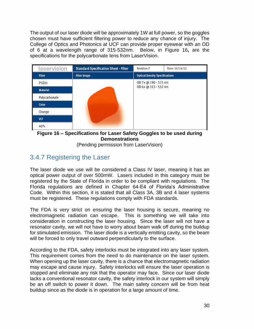
30
The output of our laser diode will be approximately 1W at full power, so the goggles chosen must have sufficient filtering power to reduce any chance of injury. The College of Optics and Photonics at UCF can provide proper eyewear with an OD of 6 at a wavelength range of 315-532nm. Below, in Figure 16, are the specifications for the polycarbonate lens from LaserVision.
Figure 16 – Specifications for Laser Safety Goggles to be used during
Demonstrations (Pending permission from LaserVision)
3.4.7 Registering the Laser The laser diode we use will be considered a Class IV laser, meaning it has an optical power output of over 500mW. Lasers included in this category must be registered by the State of Florida in order to be compliant with regulations. The Florida regulations are defined in Chapter 64-E4 of Florida’s Administrative Code. Within this section, it is stated that all Class 3A, 3B and 4 laser systems must be registered. These regulations comply with FDA standards. The FDA is very strict on ensuring the laser housing is secure, meaning no electromagnetic radiation can escape. This is something we will take into consideration in constructing the laser housing. Since the laser will not have a resonator cavity, we will not have to worry about beam walk off during the buildup for stimulated emission. The laser diode is a vertically emitting cavity, so the beam will be forced to only travel outward perpendicularly to the surface. According to the FDA, safety interlocks must be integrated into any laser system. This requirement comes from the need to do maintenance on the laser system. When opening up the laser cavity, there is a chance that electromagnetic radiation may escape and cause injury. Safety interlocks will ensure the laser operation is stopped and eliminate any risk that the operator may face. Since our laser diode lacks a conventional resonator cavity, the safety interlock in our system will simply be an off switch to power it down. The main safety concern will be from heat buildup since as the diode is in operation for a large amount of time.
31
Another requirement for the FDA is an emission indicator. This will do exactly as the name implies, when the laser operating, a light will illuminate indicating that the beam is hot. This is just an additional safety measure so any observer will know that the beam is being fired. In our system the emission indicator will be a simple LED integrated into the laser housing. A beam attenuator is also required for a laser system. Usually this can be a mechanical shutter that blocks the beam emission without shutting down the resonator cavity. For our diode we’ll use an electrical shutter that cuts the current to stop operation. The threshold time is very minimal so it won’t be of concern when we power the diode up again. The FDA also defines labelling requirements appropriate to the class of laser we will be using. Since Class 1 lasers have a very small power output, a label is not required. A ‘Caution’ label is required for low power output Class 2 and 3b lasers. Any laser producing an irradiance greater than 2.5x10⁻³ W cm-2 must have a ‘Danger’ label. After we ensure that every aspect of our laser system is compliant with FDA regulations, the final step to registering our laser is to fill out the DH Form 1605, which is meant for laser owners not laser manufactures. This form is to be sent to the Florida Bureau of Radiation Control.
3.5 Video Capture System Central to any design which involves computer-vision is the image sensor subsystem. Such systems need to capture frames of light and properly digitize them such that an image that accurately conveys the view of a scene can be handed off to the primary processing component. However, the choice of an image sensor subsystem requires us to look at a variety of factors. These factors include frame rate, field of view, resolution, image detail, and of course cost. The trade-offs with these are between frame rate and resolution, and between field of view and image detail. Frame rate in this case refers to how quickly frames are sent to the main processor. This is impacted primarily by the number of pixels used to represent the image, or resolution. If an image is represented by a larger pixel map, then the system must be more powerful in order to maintain a good frame rate. The field of view, is basically the degree measurement of how much of a scene is represented in the image, wherein 360° would mean that the image represents a view of everything around the camera the azimuthal axis. A large frame of view, however, means that more of the image must be represented by fewer pixels, thus meaning less image detail. Each of these factors can be improved upon by simply buying a more expensive camera system, but these systems quickly become grossly expensive. Another factor to consider when selecting the image sensor subsystem is the complexity of implementing the system. For instance, if one desired to, they could purchase the camera and digital signal processor separately, and then work to
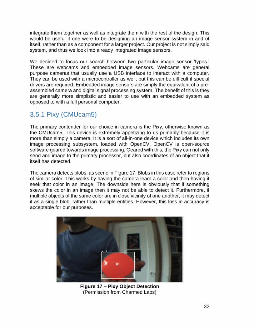
32
integrate them together as well as integrate them with the rest of the design. This would be useful if one were to be designing an image sensor system in and of itself, rather than as a component for a larger project. Our project is not simply said system, and thus we look into already integrated image sensors. We decided to focus our search between two particular image sensor ‘types.’ These are webcams and embedded image sensors. Webcams are general purpose cameras that usually use a USB interface to interact with a computer. They can be used with a microcontroller as well, but this can be difficult if special drivers are required. Embedded image sensors are simply the equivalent of a pre-assembled camera and digital signal processing system. The benefit of this is they are generally more simplistic and easier to use with an embedded system as opposed to with a full personal computer.
3.5.1 Pixy (CMUcam5) The primary contender for our choice in camera is the Pixy, otherwise known as the CMUcam5. This device is extremely appetizing to us primarily because it is more than simply a camera. It is a sort of all-in-one device which includes its own image processing subsystem, loaded with OpenCV. OpenCV is open-source software geared towards image processing. Geared with this, the Pixy can not only send and image to the primary processor, but also coordinates of an object that it itself has detected. The camera detects blobs, as scene in Figure 17. Blobs in this case refer to regions of similar color. This works by having the camera learn a color and then having it seek that color in an image. The downside here is obviously that if something skews the color in an image then it may not be able to detect it. Furthermore, if multiple objects of the same color are in close vicinity of one another, it may detect it as a single blob, rather than multiple entities. However, this loss in accuracy is acceptable for our purposes.
Figure 17 – Pixy Object Detection
(Permission from Charmed Labs)
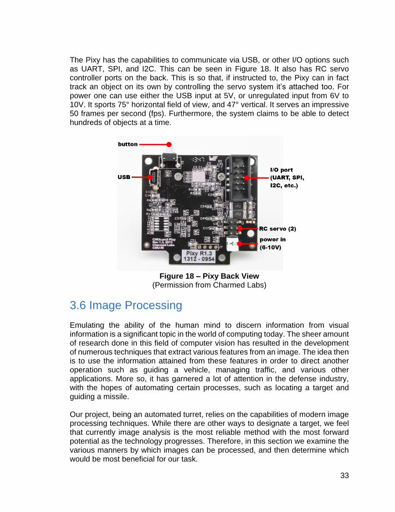
33
The Pixy has the capabilities to communicate via USB, or other I/O options such as UART, SPI, and I2C. This can be seen in Figure 18. It also has RC servo controller ports on the back. This is so that, if instructed to, the Pixy can in fact track an object on its own by controlling the servo system it’s attached too. For power one can use either the USB input at 5V, or unregulated input from 6V to 10V. It sports 75° horizontal field of view, and 47° vertical. It serves an impressive 50 frames per second (fps). Furthermore, the system claims to be able to detect hundreds of objects at a time.
Figure 18 – Pixy Back View
(Permission from Charmed Labs)
3.6 Image Processing Emulating the ability of the human mind to discern information from visual information is a significant topic in the world of computing today. The sheer amount of research done in this field of computer vision has resulted in the development of numerous techniques that extract various features from an image. The idea then is to use the information attained from these features in order to direct another operation such as guiding a vehicle, managing traffic, and various other applications. More so, it has garnered a lot of attention in the defense industry, with the hopes of automating certain processes, such as locating a target and guiding a missile. Our project, being an automated turret, relies on the capabilities of modern image processing techniques. While there are other ways to designate a target, we feel that currently image analysis is the most reliable method with the most forward potential as the technology progresses. Therefore, in this section we examine the various manners by which images can be processed, and then determine which would be most beneficial for our task.

34
As state, there are many techniques for processing images in order to retrieve information about various features of a scene. Furthermore, each technique has many variations. The choice of algorithm often depends on how much processing power is available and then how accurate the results need to be. For instance, facial recognition requires a lot of processing power and then to appropriately recognize the face a fair degree of accuracy is needed. However, if you merely want to detect movement, you need very little power and a false detect every now and then may not be as detrimental.
3.6.1 Edge Detection Edge detection is one of the simplest techniques to apply upon an image, and it can be one of the most useful for discerning different objects or separating out a background. The technique itself involves highlighting edges which are generally the boundaries of objects or where there is a significant change in brightness or color. Its great simplicity can also result in severe inaccuracies, however, depending on the chosen algorithm. In many cases results may contain fragmentation, which involves disconnected edges in a complex image, or edges may be lost due to similar colors and smooth brightness transitions. An example edge detection can be seen in Figure 19 below.
Figure 19 – Edge Detection Example
“Canny edge detection applied to a photograph” by JonMcLoone is licensed under CC-BY-SA 3.0
One of the most well-known techniques for edge detection, is Canny edge detection. This method, developed by John Canny, involves four primary steps: (1) the application of a Gaussian filter to remove noise via blurring, (2) the application of a gradient operator to attain the intensity and direction of gradients, (3) non-maximum suppression, and (4) hysteresis thresholding [2]. Simply put, the technique looks for locations where the change in brightness or color is greatest in some direction along the pixels in that location. The Canny method is known as a first order method, because it uses first order differentiation in order to attain its results. This differentiation is done by the edge
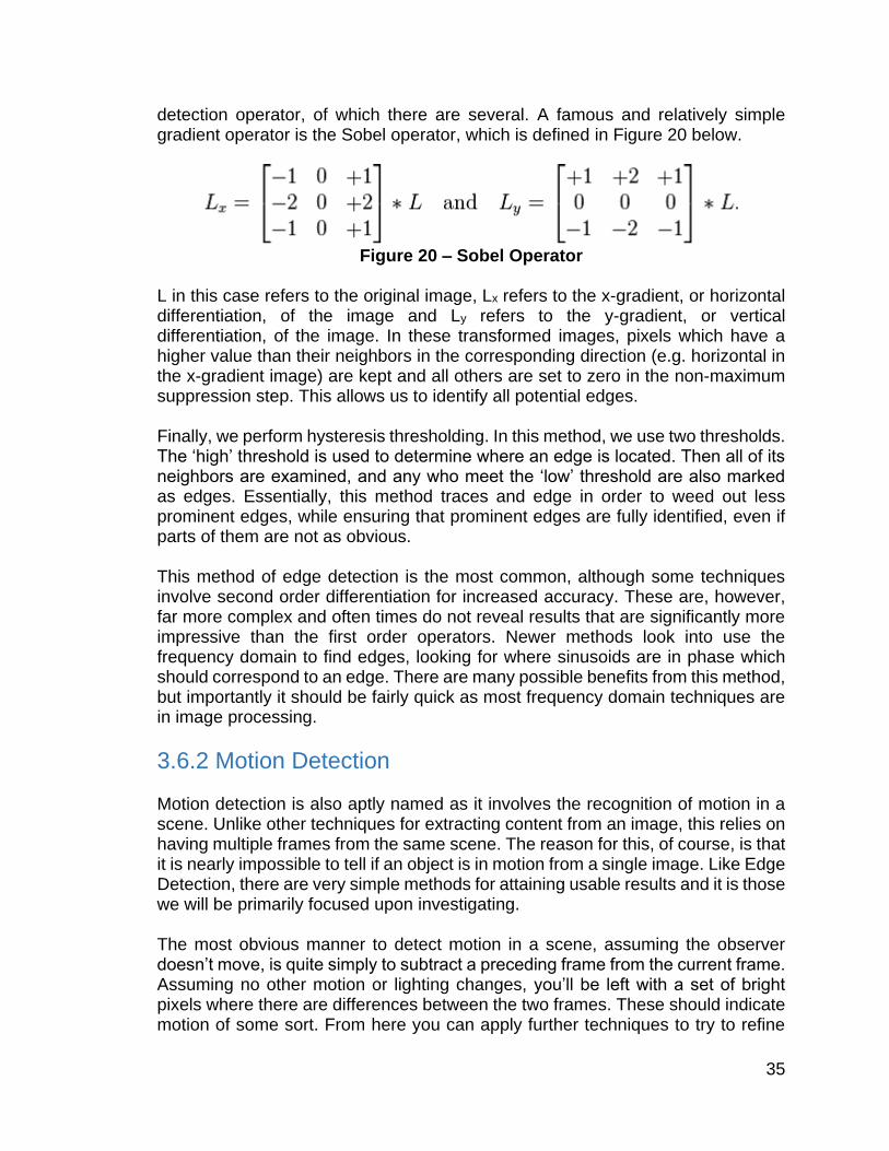
35
detection operator, of which there are several. A famous and relatively simple gradient operator is the Sobel operator, which is defined in Figure 20 below.
Figure 20 – Sobel Operator
L in this case refers to the original image, Lx refers to the x-gradient, or horizontal differentiation, of the image and Ly refers to the y-gradient, or vertical differentiation, of the image. In these transformed images, pixels which have a higher value than their neighbors in the corresponding direction (e.g. horizontal in the x-gradient image) are kept and all others are set to zero in the non-maximum suppression step. This allows us to identify all potential edges. Finally, we perform hysteresis thresholding. In this method, we use two thresholds. The ‘high’ threshold is used to determine where an edge is located. Then all of its neighbors are examined, and any who meet the ‘low’ threshold are also marked as edges. Essentially, this method traces and edge in order to weed out less prominent edges, while ensuring that prominent edges are fully identified, even if parts of them are not as obvious. This method of edge detection is the most common, although some techniques involve second order differentiation for increased accuracy. These are, however, far more complex and often times do not reveal results that are significantly more impressive than the first order operators. Newer methods look into use the frequency domain to find edges, looking for where sinusoids are in phase which should correspond to an edge. There are many possible benefits from this method, but importantly it should be fairly quick as most frequency domain techniques are in image processing.
3.6.2 Motion Detection Motion detection is also aptly named as it involves the recognition of motion in a scene. Unlike other techniques for extracting content from an image, this relies on having multiple frames from the same scene. The reason for this, of course, is that it is nearly impossible to tell if an object is in motion from a single image. Like Edge Detection, there are very simple methods for attaining usable results and it is those we will be primarily focused upon investigating. The most obvious manner to detect motion in a scene, assuming the observer doesn’t move, is quite simply to subtract a preceding frame from the current frame. Assuming no other motion or lighting changes, you’ll be left with a set of bright pixels where there are differences between the two frames. These should indicate motion of some sort. From here you can apply further techniques to try to refine
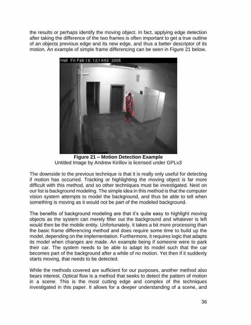
36
the results or perhaps identify the moving object. In fact, applying edge detection after taking the difference of the two frames is often important to get a true outline of an objects previous edge and its new edge, and thus a better descriptor of its motion. An example of simple frame differencing can be seen in Figure 21 below.
Figure 21 – Motion Detection Example
Untitled Image by Andrew Kirillov is licensed under GPLv3 The downside to the previous technique is that it is really only useful for detecting if motion has occurred. Tracking or highlighting the moving object is far more difficult with this method, and so other techniques must be investigated. Next on our list is background modeling. The simple idea in this method is that the computer vision system attempts to model the background, and thus be able to tell when something is moving as it would not be part of the modeled background. The benefits of background modeling are that it’s quite easy to highlight moving objects as the system can merely filter out the background and whatever is left would then be the mobile entity. Unfortunately, it takes a bit more processing than the basic frame differencing method and does require some time to build up the model, depending on the implementation. Furthermore, it requires logic that adapts its model when changes are made. An example being if someone were to park their car. The system needs to be able to adapt its model such that the car becomes part of the background after a while of no motion. Yet then if it suddenly starts moving, that needs to be detected. While the methods covered are sufficient for our purposes, another method also bears interest. Optical flow is a method that seeks to detect the pattern of motion in a scene. This is the most cutting edge and complex of the techniques investigated in this paper. It allows for a deeper understanding of a scene, and
37
furthermore lends itself to such tasks as 3D approximations and motion prediction. The usefulness, however, is limited in our application.
3.6.3 Object Recognition Recognizing objects is a significant challenge in computer vision, due to the dynamic nature of reality. The primary application of such technology mostly dwell in the realm of artificial intelligence, allowing machines to make decisions based upon a greater understanding of a scene. For our purposes, this is an extremely important field as an automated turret must identify its target in order to destroy it. As such it’s a topic which has received a lot of attention and research in the last several years. Through this research a significant amount of advances have been made and a multitude of techniques have been developed. These are generally split into two types: appearance-based and feature-based. We focus on the simpler appearance-based methods. Appearance based techniques general try to match based on similarities to a template image. A single image, of course, is very limiting as it would neglect different possible conditions, such as lighting and orientation. The trick then is to compile a large set of images of an object in order to capture it under a variety of different parameters. This collection of sample images is then known as the training set. A detected object is matched against several training sets and then is marked as the one which has the highest match score, or is marked unknown is the score is not significant enough (this varies from method to method.) An example of an appearance based method is to compare the edges of an object. Calling back to the edge detection methods, one can try to match an object based upon its outline. This method benefits mainly it that lighting conditions have little effect on the outline of an object. The actual matching can be done with various methods such as directly counting how many edges overlay with an aggregate sample image, or using probability distributions in order to attain an approximate likelihood of if an object belongs to the set being tested.
3.7 Printed Circuit Board (PCB) A printed circuit board is an integral component of an embedded system to allow our other components to work properly. A PCB electrically connects components of a circuit by etching wires into copper sheets. PCBs can be single sided, double sided or multi layered. The more layers developed, the larger the area of the board, yielding the capability to develop a larger circuit with more components. The actual PCB is developed by using several different materials. Fiberglass, historically, is the most common base substrate for the PCB. A thin layer of copper is then laminated to the board, using heat and adhesive, in order to help conduct electricity through the board. A solder mask is then applied on top of the copper

38
layer in order to insulate the copper wires and remove any possibility of contact with other conductive parts. This layer is also used in order to help the user solder components to the overall board. A silkscreen layer is then applied onto the solder mask to help the user understand the purposes of the components on the board and their values is needed. For our system, we will be required to design and develop a printed circuit board in order to incorporate our microcontrollers and cameras into the system. In order to do this, there are several different Cad software’s that are available. We compared Cadence Orcad, Eagle Cad and FreePCB to decide which the best for our needs. Orcad and Eagle Cad have free versions while FreePCB is freeware. After consideration, we decided to use Eagle Cad as our PCB design software because of its extensive part libraries and user friendliness.
3.7.1 Component Packages There are different forms of components that can be used in order to build a PCB. The three form of packages are Point-to-Point Technology, Through-Hole Technology and Surface Mount Technology. Point-to-Point technology is the oldest form of packaging methods. The components are directly soldered and wired together (similar to a breadboard) from one node to another. The nodes are then mounted onto the actual PCB using various different materials, such as screws and tape. Point-to-Point technology is not used much anymore because of the possibility of shorting out components due to exposed wire leads. Also, the solder can become loose and come off to due vibration to the PCB. Through-Hole Technology, is another form of packaging a PCB. For Through-Hole technology, the actual discrete form of the component is used (the same components used in a breadboard) and are directly inserted into the PCB. Each PCB has holes printed out for the two leads (or however many leads are on the component) and the user manually inserts the components into the correct holes, and in the correct direction, and then the leads are soldered to the board. Through-Hole technology is great for prototyping and easy to solder which makes this form of packaging great for beginners. However, Through-Hole technology requires a larger surface area for the PCB, due to larger components. Because of this, the cost of the PCB is larger. Surface Mount Technology has become the most popular form of PCB packaging. Each components’ pins are soldered to pads rather than through the holes in the PCB on the Through-Hole Technology board. Because the pads are soldered, and not the pins, this allows smaller packages for each component and each component is cheaper. However, because of the size and the pads, it is very difficult to solder these components to the board by hand. For this project, we will

39
use a mixture of Through-Hole and Surface Mount technology to take advantage of both technologies.
3.8 Communication Technology Having wireless technology for our targeting system is critical to both the success of the system, but all to provide the most safety towards the users. Having a laser in our system (that is autonomous) can become dangerous when firing towards objects. The laser theoretically could fire into an individual’s eye causing damage. Having wireless communication to send a pulse to the system giving the signal to fire the laser will prevent this. For our system, we have several requirements for the wireless technology. The wireless communication must transmit a minimum distance of 10 feet to the user. Also, the rate that the data is sent to the user must be a minimum of 15 kbps. This mixture of requirements will allow complete communication between the user and the system in order to send the required signals to the system for a successful target. For this project, three different forms of communication will be used: USB, Bluetooth and Wi-Fi. The wireless communication will be used to interact with the user interface. For this project, our targeting system is to be run at real-time. This is a large factor in determining which type of wireless communication to use. Look at Table 6 below to see the comparisons between the wireless communication options.
Table 6 – Wireless Communication Comparison
Bluetooth Wi-Fi Wireless
USB ZigBee
Frequency 2.4 GHz 2.4, 3.6, 5 GHz 3.1 – 10.6
GHz 2.4 GHz
Bandwidth 800 Kbps 11 Mbps 53-480 Mbps
250 kbps
Range 5-30 meters
32 – 95 meters depending on location and network type
3-10 meters 10-100 meters
Power Consumption
Low High High Low
3.8.1 Wi-Fi Wi-Fi communications have a lot of variability in their power due to development in Wi-Fi technologies. Based on the speed and bandwidth required for the system, a specific version of Wi-Fi technology can be chosen. Wi-Fi also ranges in various frequency bands allowing for more versatility. Through Wi-Fi, both parties can send and receive data. While Wi-Fi is not the cheapest communication option, it
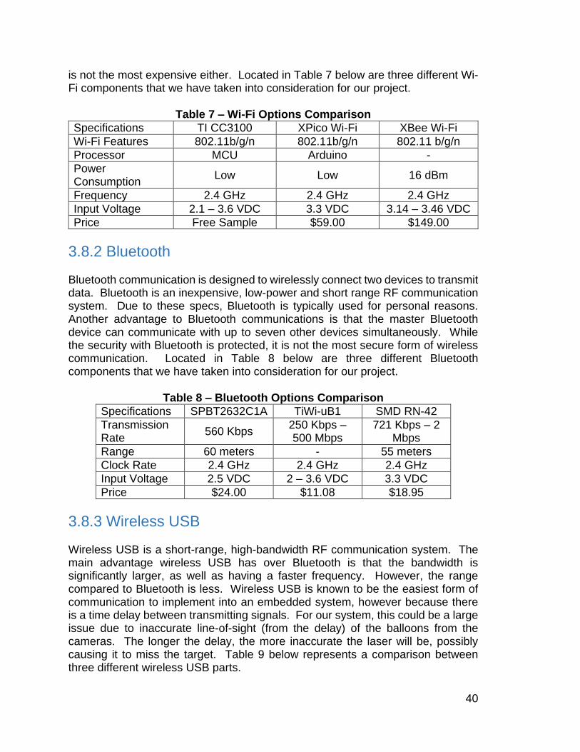
40
is not the most expensive either. Located in Table 7 below are three different Wi-Fi components that we have taken into consideration for our project.
Table 7 – Wi-Fi Options Comparison
Specifications TI CC3100 XPico Wi-Fi XBee Wi-Fi
Wi-Fi Features 802.11b/g/n 802.11b/g/n 802.11 b/g/n
Processor MCU Arduino -
Power Consumption
Low Low 16 dBm
Frequency 2.4 GHz 2.4 GHz 2.4 GHz
Input Voltage 2.1 – 3.6 VDC 3.3 VDC 3.14 – 3.46 VDC
Price Free Sample $59.00 $149.00
3.8.2 Bluetooth Bluetooth communication is designed to wirelessly connect two devices to transmit data. Bluetooth is an inexpensive, low-power and short range RF communication system. Due to these specs, Bluetooth is typically used for personal reasons. Another advantage to Bluetooth communications is that the master Bluetooth device can communicate with up to seven other devices simultaneously. While the security with Bluetooth is protected, it is not the most secure form of wireless communication. Located in Table 8 below are three different Bluetooth components that we have taken into consideration for our project.
Table 8 – Bluetooth Options Comparison
Specifications SPBT2632C1A TiWi-uB1 SMD RN-42
Transmission Rate
560 Kbps 250 Kbps – 500 Mbps
721 Kbps – 2 Mbps
Range 60 meters - 55 meters
Clock Rate 2.4 GHz 2.4 GHz 2.4 GHz
Input Voltage 2.5 VDC 2 – 3.6 VDC 3.3 VDC
Price $24.00 $11.08 $18.95
3.8.3 Wireless USB Wireless USB is a short-range, high-bandwidth RF communication system. The main advantage wireless USB has over Bluetooth is that the bandwidth is significantly larger, as well as having a faster frequency. However, the range compared to Bluetooth is less. Wireless USB is known to be the easiest form of communication to implement into an embedded system, however because there is a time delay between transmitting signals. For our system, this could be a large issue due to inaccurate line-of-sight (from the delay) of the balloons from the cameras. The longer the delay, the more inaccurate the laser will be, possibly causing it to miss the target. Table 9 below represents a comparison between three different wireless USB parts.

41
Table 9 – Wireless USB Options Comparison
Specifications Cisco Linksys
AE1000 TRENDnet
TEW-664UB
Netgear RangeMax
WNDA 3100
Bands 2.4 GHz and 5
GHz 5.150 GHz
2.4 GHz or 5 GHz
Technology Wireless-N Wireless-N Wireless-N
Antennas 2 2 2
Data Transfer Rate
300 Mbps 54 Mbps 300 Mbps
Price $99.00 $28.65 $38.95
3.8.4 ZigBee ZigBee is another form of wireless communication that can be applied to an embedded system. Similarly, to other forms of wireless communication, ZigBee utilizes radio frequencies in order to transmit data to multiple devices. One major advantage towards ZigBee is its low power consumption characteristics. Because it is low power, the bandwidth from the system is lower than the other forms of communication. For our project, because the data sent from the system to the user interface will not contain large amounts of data, ZigBee communications would be an ideal form of sending signals wirelessly to the system. ZigBee also is designed to be cheaper and easier to use than any other form of wireless communications, including the other wireless communications discussed in this section. Located in Table 10 below are three different ZigBee components that we have taken into consideration for our project.
Table 10 – ZigBee Component Comparisons
Specifications XBee Pro 868 XBee 802.15.4 XBee DigiMesh
2.4
Frequency 2.4 GHz 2.4 GHz 2.4 GHz
Topology Point-to-Multipoint
Point-to-Multipoint
Mesh
RF Data Rate 24 Kbps 250 Kbps 250 Kbps
Range 550 meters 30 meters 30 meters
Transmit Power 1 mW – 315 mW 1 mW 1 mW
Supply Voltage 3.0 – 3.6 VDC 2.8 – 3.4 VDC 2.8 – 3.4 VDC
Serial Data Rate 1.2 Kbps – 230.4
Kbps - 115.2 Kbps
Price $45.00 $19.00 $19.00

42
3.9 Gimbal Assembly
3.9.1 Gimbal Motors
The gimbal assembly will provide the ranges of motion necessary for our laser to engage the targets. If this defense system were to be used in an aerial vehicle, the gimbal motor would need to be as stable as possible to remain accurate. Since our project is terrestrial and stationary, the gimbal system will not be subject to vibrations and jitter due to movement. When it comes to choosing a gimbal to mount the laser on, there are a few options: using a brushless, stepper or servo motor. Brushless motors are powered by a DC source which is then converted to an AC signal to move the motor. Generally the rotor of the brushless motor is induced into motion by electromagnets. These are also beneficial since we can use a microcontroller to control the speed and direction of the motor. Another important factor is that these motors are very stable so when the laser is setting its sights on the target, we can be confident in the accuracy. However since our system is stationary, the added stability will not be entirely necessary. Also brushless motors are an expensive option for our applications. Stepper motors is a type of brushless motor but instead of having a continuous rotation, the rotation is divided into a specific number of increments. An example of one of these motors can be seen in Figure 22. These motors are driven by an external microcontroller and when supplied with a pulsed signal, the motor rotate to a discrete, specific location. Since the motor has a finite number of steps, we can tune the motor to an exact position. There are two type of stepper motors: permanent magnet and variable-reluctance motors. The former is pushed to rotation by the opposing forces of a permanent magnet, which is in the rotor, and the electromagnetic field generated from the current. When the poles of the rotor and electromagnetic field align, the motor comes to a rest. When the electromagnetic field is changed, the motor then begins to rotate again. A variable-reluctance stepper motor has a series of stationary coils. The rotor is at the center of the coils. When a pulse is sent, it charges two opposing coils with opposite charge. This is what causes the motor to rotate. One downside is that stepper motors are open loop systems. This system assumes that motion has taken place already. If our motor was jammed, the controller would not realize this and continue to send pulses with no action happening.
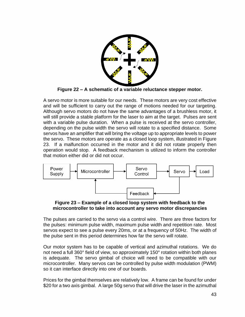
43
Figure 22 – A schematic of a variable reluctance stepper motor.
A servo motor is more suitable for our needs. These motors are very cost effective and will be sufficient to carry out the range of motions needed for our targeting. Although servo motors do not have the same advantages of a brushless motor, it will still provide a stable platform for the laser to aim at the target. Pulses are sent with a variable pulse duration. When a pulse is received at the servo controller, depending on the pulse width the servo will rotate to a specified distance. Some servos have an amplifier that will bring the voltage up to appropriate levels to power the servo. These motors are operate as a closed loop system, illustrated in Figure 23. If a malfunction occurred in the motor and it did not rotate properly then operation would stop. A feedback mechanism is utilized to inform the controller that motion either did or did not occur.
Figure 23 – Example of a closed loop system with feedback to the
microcontroller to take into account any servo motor discrepancies
The pulses are carried to the servo via a control wire. There are three factors for the pulses: minimum pulse width, maximum pulse width and repetition rate. Most servos expect to see a pulse every 20ms, or at a frequency of 50Hz. The width of the pulse sent in this period determines how far the servo will rotate. Our motor system has to be capable of vertical and azimuthal rotations. We do not need a full 360° field of view, so approximately 150° rotation within both planes is adequate. The servo gimbal of choice will need to be compatible with our microcontroller. Many servos can be controlled by pulse width modulation (PWM) so it can interface directly into one of our boards. Prices for the gimbal themselves are relatively low. A frame can be found for under $20 for a two axis gimbal. A large 50g servo that will drive the laser in the azimuthal

44
plane costs approximately $15. Most gimbals use a smaller 9g servo for vertical rotations, which cost around $15 for a higher end model. In total, we should not spend more than $50 in total for the gimbal assembly.
3.10 Power Supply Due to the complexity of the overall system, the targeting system will contain several different components. Each component has its own voltage and current requirements to power on, as well as voltage and power maximums so that the components do not burn out. Table 11 below shows the required voltages and currents for each component.
Table 11 – Required Voltage for Components
Component Peak Voltage Peak Current Amount Peak Power
Cameras 10 V 140 mA 2 2.8 W
Motor Servos 6 V 500 mA 2 6 W
Laser 7 1.3 A 1 1.1
Microcontroller 3.6 V 120 µA 1 432 mW
The camera that we decided to use typically is powered by up to 10 V. The motor servos that we will use to gimbalize the laser are powered by the PCB but will require an extra power source because the power sent to the microcontroller will not generate enough voltage and current to turn on the servos. The typical laser pointer is powered by two AA batteries in series. Each AA battery supplies 1.5 V summing the two batteries to a total of 3 VDC. The microcontroller will be a part of the PCB and therefore will get its power from the power sent to the board. The actual microcontroller requires 3.6 volts to turn on. Our microcontroller is known for lower voltage and low power consumption. Because our system has many subsystems and components, we will need a large enough source to power the entire system. To do this, our main power supply can either be from a wall outlet or a large battery. Plugging into a wall outlet will be the cheaper and easier to implement option, but it limits where our system can be utilized. With the wall outlet, we will be restricted to the length of our extension cord while with a battery, our system will be completely mobilized. Because certain components require an AC input, we will use a form of input that will generate an AC input. A wall outlet is a great example of such a power supply.
3.11.1 Power Sources Our system will require a unique power source that will generate enough current and power to turn on all subsystems of our system. For our system, we considered the following sources of power: batteries, AC power, solar power and a generator. Each form of power supply will be taken into consideration and the best option will be utilized after comparing each form on power. An incorrect selection of power
45
supplies can either burn out our parts (if there is too much voltage) or not power them on (if there is not enough voltage applied). An ideal form of power would contain the following requirements: supply the proper amount of voltage and current, be inexpensive, having mobility and ease of connecting to the system.
3.10.1.1 Batteries Batteries are a very unique form of power because there are many different types of batteries that can be utilized. Due to the diversity of batteries types, we have several requirements that must be met if we decide to utilize batteries to power our system. Our requirements are the following: batteries must be lightweight and easy to move, batteries must hold their charge for a minimum of 2 hours, batteries must be reliable in all weather situations and environments and all batteries must be replaceable. For this project, we took the following types of batteries into consideration: alkaline, aluminum-ion, lithium-ion and nickel-cadmium. Alkaline batteries are the most common form of battery that everyday users utilize. Alkaline batteries are have a very high energy density and long shelf-life while still maintaining the same voltage. Alkaline batteries are also disposable which is why they are the most common form of battery. While these types of batteries are great, each cell ideally generates roughly 1.5 volts. Alkaline batteries can easily be put in series to increase the voltage. This will not only increase price but also increase the physical volume needed to hold all of the batteries. Alkaline batteries also generate roughly 700 mA of current which would be enough current for our system when combined in series with other alkaline batteries. Aluminum ion batteries, when compared to alkaline batteries, have a higher energy density and also cost less due to the chemical elements being cheaper. Each aluminum ion battery generates roughly 2.65 volts, which is larger than the alkaline batteries. One unique feature of the aluminum ion battery is that it is rechargeable, unlike the alkaline batteries. While aluminum ion batteries are not the most common form of battery, even as a substitute for the alkaline batteries, they are still used for everyday objects, such as consumer electronics. Lithium-ion batteries are very similar to the aluminum ion batteries except the physical chemicals used are different. Lithium ion batteries are also rechargeable and generate about 3.6 volts per cell, which is higher than the aluminum ion batteries. Lithium ion batteries are once again not used for more than consumer electronics or other everyday objects. Nickel-Cadmium batteries are not a feasible option for our system because of their low cell voltage of 12 volts. The energy density of nickel cadmium batteries is also low. The main advantage of these batteries is that they are rechargeable and can recharge up to 2000 cycles.

46
3.10.1.2 Solar Power With systems becoming more energy efficient in today’s age, we discussed making our system fully solar powered. While we did consider this for sustainability reasons, we did not investigate into solar power to much for several reasons. To have a fully solar powered system, we would have had to have several solar panels, increasing our budget, and also increasing the size of our system. We would also like to keep our system as realistic as possible. A targeting system in the real world could not depend on solar rays to power their targeting systems due to the possibility of not having any rays. Whether the system was being used at night, or simply on an overcast day, the dependability of the sun would not be a feasible option for a real world application of a targeting system.
3.10.1.3 Generators As mentioned earlier, an ideal form of power would have an AC input. While generators do in fact produce AC outputs, the output is very similar to the output from a simply wall outlet. It would be illogical to purchase a generator to power our system when we could hook up all of our power to a much cheaper AC input source. Due to this, our research in the generator field concluded without much knowledge acquired.
3.10.1.4 AC Power We believe that after consideration and comparing other forms of power supplies that our best option is to use a power strip connected to a standard wall-output to generate our power. The reason for this is the amount of power that will needed to operate a laser capable of piercing a balloon, and also for safety purposes. In the event of a failure, the system can be unplugged to prevent damage by the laser. We will get the AC input that we need for the PCB and will incorporate AC/DC converters for those subsystems that require strictly DC signals. We will also utilize voltage regulators where necessary to ensure that no subsystem or components get burnt out due to much voltage or current. This could result in our entire system failing.
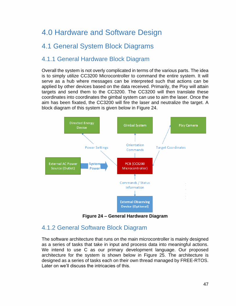
47
4.0 Hardware and Software Design
4.1 General System Block Diagrams
4.1.1 General Hardware Block Diagram Overall the system is not overly complicated in terms of the various parts. The idea is to simply utilize CC3200 Microcontroller to command the entire system. It will serve as a hub where messages can be interpreted such that actions can be applied by other devices based on the data received. Primarily, the Pixy will attain targets and send them to the CC3200. The CC3200 will then translate these coordinates into coordinates the gimbal system can use to aim the laser. Once the aim has been fixated, the CC3200 will fire the laser and neutralize the target. A block diagram of this system is given below in Figure 24.
Figure 24 – General Hardware Diagram
4.1.2 General Software Block Diagram The software architecture that runs on the main microcontroller is mainly designed as a series of tasks that take in input and process data into meaningful actions. We intend to use C as our primary development language. Our proposed architecture for the system is shown below in Figure 25. The architecture is designed as a series of tasks each on their own thread managed by FREE-RTOS. Later on we’ll discuss the intricacies of this.
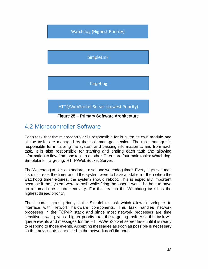
48
Figure 25 – Primary Software Architecture
4.2 Microcontroller Software Each task that the microcontroller is responsible for is given its own module and all the tasks are managed by the task manager section. The task manager is responsible for initializing the system and passing information to and from each task. It is also responsible for starting and ending each task and allowing information to flow from one task to another. There are four main tasks: Watchdog, SimpleLink, Targeting, HTTP/WebSocket Server. The Watchdog task is a standard ten second watchdog timer. Every eight seconds it should reset the timer and if the system were to have a fatal error then when the watchdog timer expires, the system should reboot. This is especially important because if the system were to rash while firing the laser it would be best to have an automatic reset and recovery. For this reason the Watchdog task has the highest thread priority. The second highest priority is the SimpleLink task which allows developers to interface with network hardware components. This task handles network processes in the TCP/IP stack and since most network processes are time sensitive it was given a higher priority than the targeting task. Also this task will queue events and messages for the HTTP/WebSocket server task until it is ready to respond to those events. Accepting messages as soon as possible is necessary so that any clients connected to the network don’t timeout.
SimpleLink
Targeting
HTTP/WebSocket Server (Lowest Priority)
Watchdog (Highest Priority)

49
The Targeting task is responsible for signaling the camera for the image data and identifying the current target or if a valid target exists at all. This task should return the coordinates of the current target. If there is no valid target then null coordinates should be returned. Otherwise if there is more than one valid target, the task should prioritize the targets either by distance or closeness to the line of fire and return the highest priority target to the task manager. Image processing will not occur in this task because object identification is very intensive on the main microcontroller. Instead object identification work is offloaded to another microcontroller on the Pixy camera which runs its own software architecture to interface with the camera and identify objects. Table 12 shows the functions created for target acquisition. Once the Targeting task has the coordinates of the current target, then it sends movement info to the servos. This task is also responsible for re-orientating the turret so that the current target is in the line of fire. Given the coordinates of the current target the Targeting task must calculate the angles for yaw and pitch that the turret must rotate by to fire on the target. Once these angles have been calculated, the task should realize these movements by using the pulse width modulation outputs to control two servo motors. This task can also receive messages from the external interface through the task manager to manually rotate the turret. Finally the task should return status information back to the task manager such as the calculated angles and current orientation of the turret. Table 13 shows the functions created for turret movement. After the turret has reoriented itself to the target, the Targeting task must decide whether or not to fire the laser. Given the coordinates of the target and the current orientation of the turret, this task should determine if the target is in the line of fire. If it is then the laser should be turned on via digital output to the laser driver. Otherwise the laser should be turned off. Also the task manager should pass any flags set by the user to this task. For example through the external interface the user may set a flag as to whether the laser is enabled or disabled. If the laser is disabled then even if a target is in the line of fire, the laser should not turn on. This task returns the current status of the laser to the task manager (whether or not it is firing). Table 14 shows the functions created for fire control. The last task is to handle communications with the external interface and the main microcontroller and is known as the HTTP/WebSocket task. Generally messages that reach the application layer have a long timeout period so this task is given the lowest priority. Even though the CC3200 does come with a HTTP web server, communicating through HTTP POST/GET was slow and had too much overhead. It also did not support WebSockets which would significantly speed up communications. So it was decided to implement a custom web server that could serve up web pages like the default server, but had the added ability to establish WebSockets as well. Table 15 shows the functions created for external communication.
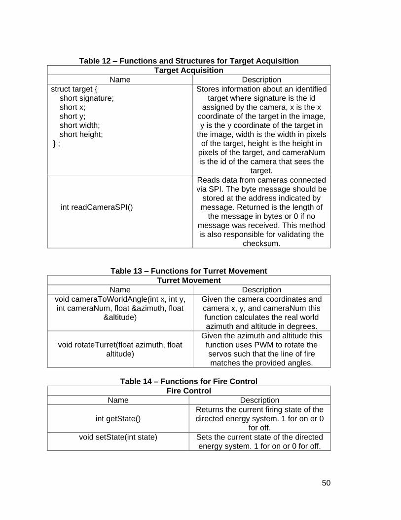
50
Table 12 – Functions and Structures for Target Acquisition
Target Acquisition
Name Description
struct target { short signature; short x; short y; short width; short height; } ;
Stores information about an identified target where signature is the id
assigned by the camera, x is the x coordinate of the target in the image, y is the y coordinate of the target in
the image, width is the width in pixels of the target, height is the height in
pixels of the target, and cameraNum is the id of the camera that sees the
target.
int readCameraSPI()
Reads data from cameras connected via SPI. The byte message should be
stored at the address indicated by message. Returned is the length of
the message in bytes or 0 if no message was received. This method is also responsible for validating the
checksum.
Table 13 – Functions for Turret Movement
Turret Movement
Name Description
void cameraToWorldAngle(int x, int y, int cameraNum, float &azimuth, float
&altitude)
Given the camera coordinates and camera x, y, and cameraNum this function calculates the real world azimuth and altitude in degrees.
void rotateTurret(float azimuth, float
altitude)
Given the azimuth and altitude this function uses PWM to rotate the servos such that the line of fire matches the provided angles.
Table 14 – Functions for Fire Control
Fire Control
Name Description
int getState()
Returns the current firing state of the directed energy system. 1 for on or 0
for off.
void setState(int state) Sets the current state of the directed energy system. 1 for on or 0 for off.
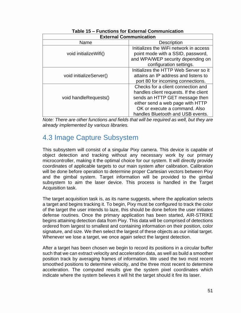
51
Table 15 – Functions for External Communication
External Communication
Name Description
void initializeWifi()
Initializes the WiFi network in access point mode with a SSID, password,
and WPA/WEP security depending on configuration settings.
void initializeServer()
Initializes the HTTP Web Server so it attains an IP address and listens to port 80 for incoming connections.
void handleRequests()
Checks for a client connection and handles client requests. If the client sends an HTTP GET message then either send a web page with HTTP OK or execute a command. Also
handles Bluetooth and USB events.
Note: There are other functions and fields that will be required as well, but they are already implemented by various libraries.
4.3 Image Capture Subsystem This subsystem will consist of a singular Pixy camera. This device is capable of object detection and tracking without any necessary work by our primary microcontroller, making it the optimal choice for our system. It will directly provide coordinates of applicable targets to our main system after calibration. Calibration will be done before operation to determine proper Cartesian vectors between Pixy and the gimbal system. Target information will be provided to the gimbal subsystem to aim the laser device. This process is handled in the Target Acquisition task. The target acquisition task is, as its name suggests, where the application selects a target and begins tracking it. To begin, Pixy must be configured to track the color of the target the user intends to laze, this should be done before the user initiates defense routines. Once the primary application has been started, AIR-STRIKE begins attaining detection data from Pixy. This data will be comprised of detections ordered from largest to smallest and containing information on their position, color signature, and size. We then select the largest of these objects as our initial target. Whenever we lose a target, we once again select the largest detection. After a target has been chosen we begin to record its positions in a circular buffer such that we can extract velocity and acceleration data, as well as build a smoother position track by averaging frames of information. We used the two most recent smoothed positions to determine velocity, and the three most recent to determine acceleration. The computed results give the system pixel coordinates which indicate where the system believes it will hit the target should it fire its laser.

52
This information then needs to be transformed into a polar coordinate frame from which we can extract a yaw and pitch to provide the Servo. To start with we have to define our coordinate frame. We use a standard definition for our Cartesian and
Polar coordinates as seen in Figure 26, though some systems swap 𝜃 and 𝜙.
Figure 26 – Standard Cartesian and Spherical Coordinate Frame Relationship
With this defined, we then convert the pixel coordinates of our target into a polar coordinates from Pixy’s perspective. Pixy coordinates are defined as xp and yp, where xp is our Cartesian y, and yp is our Cartesian z. In order to being the conversion we use the equation:
𝛼𝑗⃗⃗ ⃗ =𝐷𝑗⃗⃗ ⃗
𝑃𝑗⃗⃗ (1)
where j a spatial dimension, 𝐷𝑗⃗⃗ ⃗ is the number of pixels in dimension j, 𝑃𝑗⃗⃗ is the
number of pixels available in dimension j, and 𝛼𝑗⃗⃗ ⃗ is the degrees per pixel in
dimension j.
Using this vector 𝛼 , we can transform our pixel coordinate (xp, yp) into a polar coordinate (θp, Φp). θp is 90 minus our polar θ, and Φp is simply the opposite of our polar Φ. For range, the user must input an estimated range. This gives us a standardized polar coordinate (r, θ, Φ). Now we need to convert this into a Cartesian coordinate, using the equations that follow:
𝑥 = 𝑟 ∗ sin(𝜃) ∗ cos(𝜙) (2) 𝑦 = 𝑟 ∗ sin(𝜃) ∗ sin(𝜙) (3) 𝑧 = 𝑟 ∗ cos(𝜃). (4)
Next we add these values to a pre-measured Cartesian vector which measures the distance from our laser to Pixy in order to get the Cartesian coordinates of our target from the frame of reference of our gimbal. This can then be converted back into spherical coordinates for our gimbal via the following equations:
𝑟 = √𝑥2 + 𝑦2 + 𝑧2 (5)
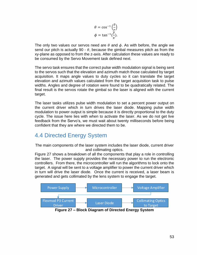
53
𝜃 = cos−1 (
𝑧
𝑟)
(6)
𝜙 = tan−1(
𝑦
𝑥). (7)
The only two values our servos need are 𝜃 and 𝜙. As with before, the angle we send our pitch is actually 90 - 𝜃, because the gimbal measures pitch as from the xy-plane as opposed to from the z-axis. After calculation these values are ready to be consumed by the Servo Movement task defined next. The servo task ensures that the correct pulse width modulation signal is being sent to the servos such that the elevation and azimuth match those calculated by target acquisition. It maps angle values to duty cycles so it can translate the target elevation and azimuth values calculated from the target acquisition task to pulse widths. Angles and degree of rotation were found to be quadratically related. The final result is the servos rotate the gimbal so the laser is aligned with the current target. The laser tasks utilizes pulse width modulation to set a percent power output on the current driver which in turn drives the laser diode. Mapping pulse width modulation to power output is simple because it is directly proportional to the duty cycle. The issue here lies with when to activate the laser. As we do not get live feedback from the Servo’s, we must wait about twenty milliseconds before being confident that they are where we directed them to be.
4.4 Directed Energy System The main components of the laser system includes the laser diode, current driver
and collimating optics. Figure 27 shows a breakdown of all the components that play a role in controlling the laser. The power supply provides the necessary power to run the electronic controllers. From there, the microcontroller will run the algorithms to lock onto the target. A signal will be sent to a voltage amplifier to power the current driver which in turn will drive the laser diode. Once the current is received, a laser beam is generated and gets collimated by the lens system to engage the target.
Power Supply Microcontroller Voltage Amplifier
Flexmod P3 Current Driver
Laser DiodeCollimating Optics
to Target Figure 27 – Block Diagram of Directed Energy System

54
4.4.2 Assemblage The assembly for the directed energy system is very straight forward. The current driver will be interfaced with the PCB board and terminal wires will be run up to the laser diode. The laser diode is mounted into a heat sink which is fitted into the gimbal assembly. Many laser diodes are packaged in a copper module heat sink which will allow us to directly screw on the collimating optics.
4.4.3 Specifications The laser diode our project will use is the S06J. This diode is commercially used in projector applications but it meets the specifications that our project requires. This type of diodes emits high energy electromagnetic radiation at a wavelength of 405nm, which is visibly blue light. Since the laser diode are very delicate, we only drove it 450mA to preserve operation lifetime. At this current level we were able to push 650mW of optical power. In order to obtain full power output, we must choose a current driver capable of achieving these currents. For this model diode, the cost will be about $89. The current driver our project will use is the Flexmod P3 driver. This driver requires an input voltage of nine volts and is capable of achieving current levels up to four amps. One benefit to this driver is that it can be controlled by pulse width modulation, so that our microcontroller can send signals indicating when to inject current into the laser diode. In order to have a variable current output, we can integrate a Darington transistor to control the PWM pulses. This transistor has PWM pins that can take the pulses from the microcontroller and reduce or increase the voltage to desired levels to power the current driver. This driver costs about $35. In order to deliver the high powered beam to the target, we must be able to collimate it to a small area for maximum beam intensity. The lens system we used are supplied by LightPath Technologies. This collimating lens are specifically coated for 445nm with anti-reflecting film. These lens have an outer aperture diameter of approximately 6mm. This allows for a numerical aperture of .66 to collect a majority of the light exiting the laser diode. They have a focal length of 4.02mm and the housing will allow us to fine tune the beam until it is collimated. For a high quality lens like this, it cost $50.
4.5 Servo Control Our gimbal will require two servo motors. Since the heat sink is mounted in the gimbal assembly, we chose to use metal gear 9g servo motors to compensate for the added weight. One of the servo motors controls rotations in the azimuthal plane, while the other has control of the vertical movement. Most servo motors are controlled by PWM, which is ideal for our microcontrollers. By controlling the
55
duration of the pulses, we can control how much the servo motor will rotate. The servo motors are the Turnigy MG90s. These motors can input 4.8V to 6V that can give operating speeds ranging from .10sec/60deg to .08sec/60deg.
4.6 Communication Systems
4.6.1 Wi-Fi Controller External Wi-Fi communication will require extensive software implementation and is the main focus of the external communication task because the team plans to implement an embedded web server and use Wi-Fi in access point mode. This decision was made because with other communication mediums such as USB or Bluetooth the client device would need a custom application on the client side in order to provide a graphical user interface for the user. Also if the team intends to support multiple platforms such as Windows, Linux, Mac OS, or Android a different application would be required for most of the platforms. Although the client platforms may vary, they all share a common application: a web browser. If the external interface was implemented through a web server that served HTML and JavaScript web pages then the system would be able to communicate with a majority of platforms. Also given that even phones have web browsers, the user would have a mobile and convenient interface right in the palm of their hand. By using a web server for external communication it will save time and make the external interface compatible with a wide variety of devices. Before the web server can be initialized, the Wi-Fi connection through the CC3200 will need to be configured properly. The CC3200 will need to be run in access point mode so that the system will create its own Wi-Fi network and other clients can connect directly to the system rather than using an intermediate network device such as a router. The Wi-Fi network can setup without encryption however given that external interface affects a directed energy system the team would like to keep unauthorized users from accessing the network. So WEP or WPA encryption also need to be configured such that only authorized users that know the password will be able to use the external interface. With the Wi-Fi network configured clients will be able to communicate with communicate with the web server. At initialization the web server will be assigned a local IP address and any client that connects to the Wi-Fi network will also be given an IP address. To start initialization a function named initializeWiFi() should be invoked. The web server will create a socket and listen for incoming connections on port 80 because that port is generally where web traffic flows through. Afterwards when the main loop calls the external interface task the web server should check for incoming clients. If there is an available client then check for an HTTP GET request to see what the client wants. Normally the client would be requesting a web page in which case the external interface would output a HTTP OK along with the HTML markup for the web page. The HTTP GET request can also be used to send commands to the web server which would then interpret the command for the microcontroller. With

56
this method it is possible to set flags such as whether the directed energy system should be on or off. However the client should mainly make post-load communications through WebSockets as it is much faster and has little overhead. The only issue with communication via a TCP based web server is that due to IP fragmentation, not all data is guaranteed to arrive at the same time. This means when receiving a message from the client, it may come in chunks rather than in one complete message. Therefore it will be necessary to have nested loops in the web server that read in the available data and store them in a buffer while waiting for the next chunk of a message to arrive. Only when the whole message arrives can it be processed. Finally due to the limited resources of the microcontroller, the client connection will need to be closed once the request has been processed. In proper web servers, the HTTP connection may be kept alive to avoid the overhead of setting up the connection all over again, but on the microcontroller making the trade-off of conserving memory to longer connection time is important because memory is severely limited. It is also assumed that only one client will connect to the web server at a time because this architecture lacks the multi-threading support needed to serve concurrent users. Figure 28 shows the architecture of the web server.
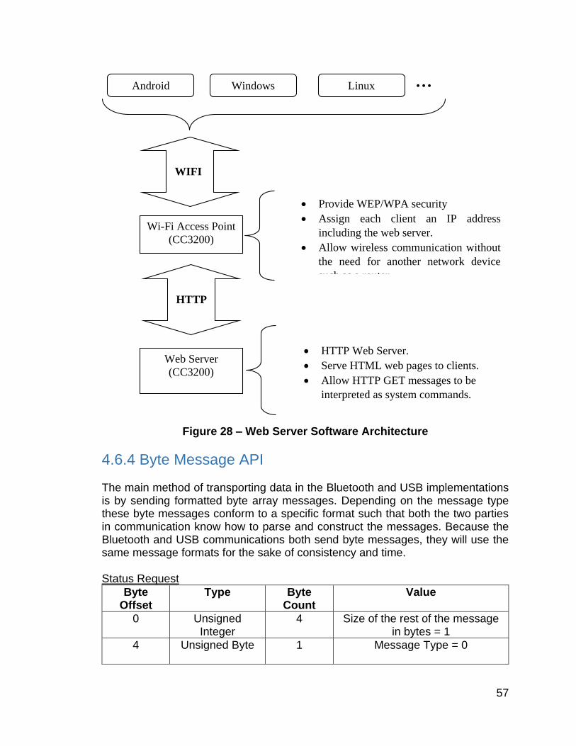
57
Figure 28 – Web Server Software Architecture
4.6.4 Byte Message API The main method of transporting data in the Bluetooth and USB implementations is by sending formatted byte array messages. Depending on the message type these byte messages conform to a specific format such that both the two parties in communication know how to parse and construct the messages. Because the Bluetooth and USB communications both send byte messages, they will use the same message formats for the sake of consistency and time. Status Request
Byte Offset
Type Byte Count
Value
0 Unsigned Integer
4 Size of the rest of the message in bytes = 1
4 Unsigned Byte 1 Message Type = 0
…
Provide WEP/WPA security
Assign each client an IP address
including the web server.
Allow wireless communication without
the need for another network device
such as a router.
HTTP Web Server.
Serve HTML web pages to clients.
Allow HTTP GET messages to be
interpreted as system commands.
Wi-Fi Access Point
(CC3200)
Android Windows Linux
WIFI
HTTP
Web Server
(CC3200)
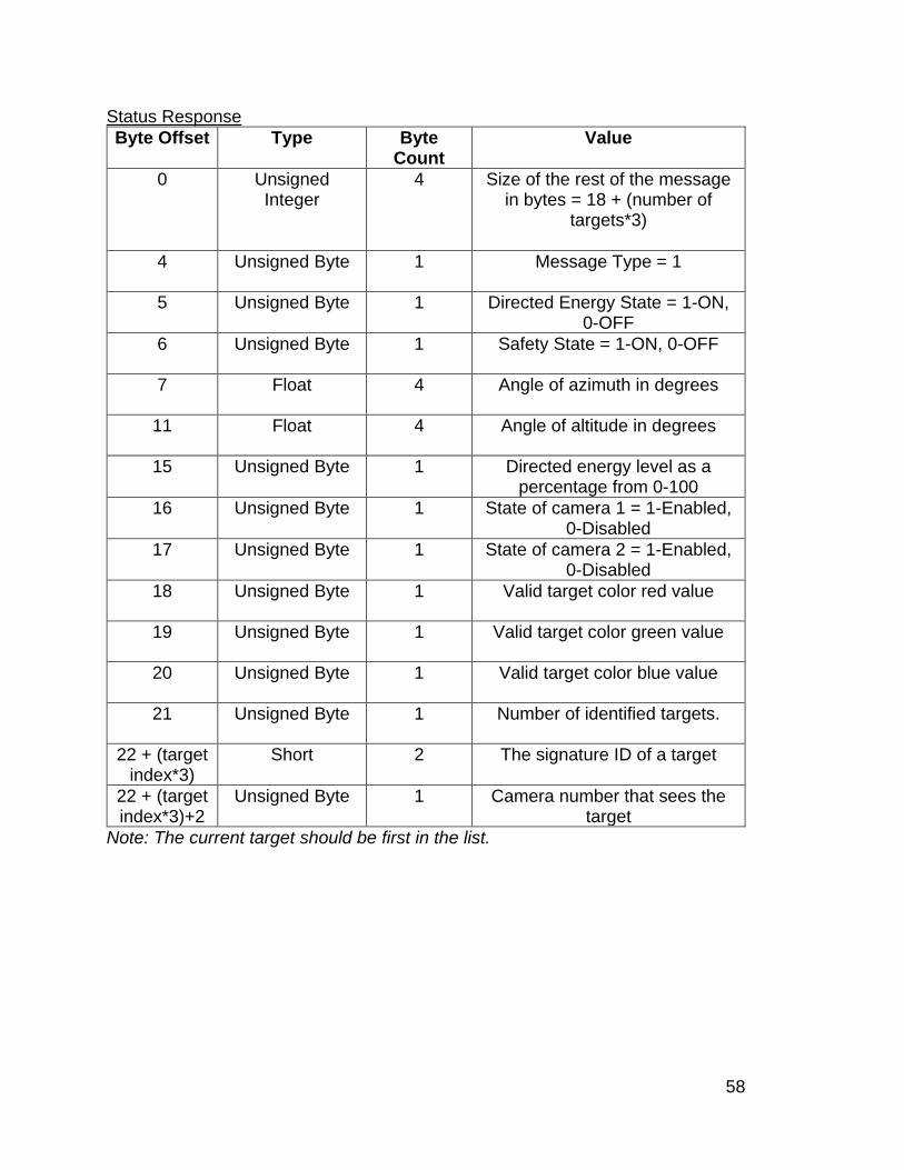
58
Status Response
Byte Offset Type Byte Count
Value
0 Unsigned Integer
4 Size of the rest of the message in bytes = 18 + (number of
targets*3)
4 Unsigned Byte 1 Message Type = 1
5 Unsigned Byte 1 Directed Energy State = 1-ON, 0-OFF
6 Unsigned Byte 1 Safety State = 1-ON, 0-OFF
7 Float 4 Angle of azimuth in degrees
11 Float 4 Angle of altitude in degrees
15 Unsigned Byte 1 Directed energy level as a percentage from 0-100
16 Unsigned Byte 1 State of camera 1 = 1-Enabled, 0-Disabled
17 Unsigned Byte 1 State of camera 2 = 1-Enabled, 0-Disabled
18 Unsigned Byte 1 Valid target color red value
19 Unsigned Byte 1 Valid target color green value
20 Unsigned Byte 1 Valid target color blue value
21 Unsigned Byte 1 Number of identified targets.
22 + (target index*3)
Short 2 The signature ID of a target
22 + (target index*3)+2
Unsigned Byte 1 Camera number that sees the target
Note: The current target should be first in the list.
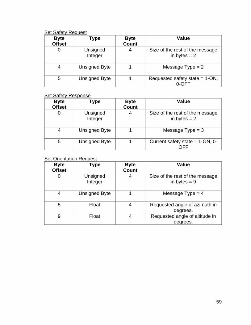
59
Set Safety Request
Byte Offset
Type Byte Count
Value
0 Unsigned Integer
4 Size of the rest of the message in bytes = 2
4 Unsigned Byte 1 Message Type = 2
5 Unsigned Byte 1 Requested safety state = 1-ON, 0-OFF
Set Safety Response
Byte Offset
Type Byte Count
Value
0 Unsigned Integer
4 Size of the rest of the message in bytes = 2
4 Unsigned Byte 1 Message Type = 3
5 Unsigned Byte 1 Current safety state = 1-ON, 0-OFF
Set Orientation Request
Byte Offset
Type Byte Count
Value
0 Unsigned Integer
4 Size of the rest of the message in bytes = 9
4 Unsigned Byte 1 Message Type = 4
5 Float 4 Requested angle of azimuth in degrees.
9 Float 4 Requested angle of altitude in degrees.
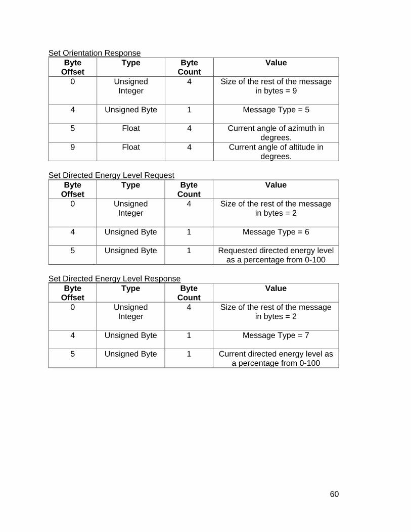
60
Set Orientation Response
Byte Offset
Type Byte Count
Value
0 Unsigned Integer
4 Size of the rest of the message in bytes = 9
4 Unsigned Byte 1 Message Type = 5
5 Float 4 Current angle of azimuth in degrees.
9 Float 4 Current angle of altitude in degrees.
Set Directed Energy Level Request
Byte Offset
Type Byte Count
Value
0 Unsigned Integer
4 Size of the rest of the message in bytes = 2
4 Unsigned Byte 1 Message Type = 6
5 Unsigned Byte 1 Requested directed energy level as a percentage from 0-100
Set Directed Energy Level Response
Byte Offset
Type Byte Count
Value
0 Unsigned Integer
4 Size of the rest of the message in bytes = 2
4 Unsigned Byte 1 Message Type = 7
5 Unsigned Byte 1 Current directed energy level as a percentage from 0-100
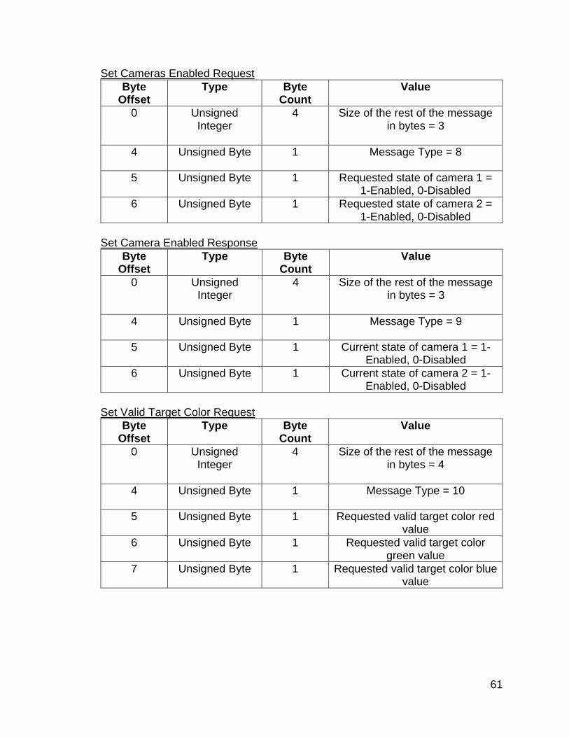
61
Set Cameras Enabled Request
Byte Offset
Type Byte Count
Value
0 Unsigned Integer
4 Size of the rest of the message in bytes = 3
4 Unsigned Byte 1 Message Type = 8
5 Unsigned Byte 1 Requested state of camera 1 = 1-Enabled, 0-Disabled
6 Unsigned Byte 1 Requested state of camera 2 = 1-Enabled, 0-Disabled
Set Camera Enabled Response
Byte Offset
Type Byte Count
Value
0 Unsigned Integer
4 Size of the rest of the message in bytes = 3
4 Unsigned Byte 1 Message Type = 9
5 Unsigned Byte 1 Current state of camera 1 = 1-Enabled, 0-Disabled
6 Unsigned Byte 1 Current state of camera 2 = 1-Enabled, 0-Disabled
Set Valid Target Color Request
Byte Offset
Type Byte Count
Value
0 Unsigned Integer
4 Size of the rest of the message in bytes = 4
4 Unsigned Byte 1 Message Type = 10
5 Unsigned Byte 1 Requested valid target color red value
6 Unsigned Byte 1 Requested valid target color green value
7 Unsigned Byte 1 Requested valid target color blue value

62
Set Valid Target Color Response
Byte Offset
Type Byte Count
Value
0 Unsigned Integer
4 Size of the rest of the message in bytes = 4
4 Unsigned Byte 1 Message Type = 11
5 Unsigned Byte 1 Current valid target color red value
6 Unsigned Byte 1 Current valid target color green value
7 Unsigned Byte 1 Current valid target color blue value
4.7 PCB Design For our PCB design, we have decided to include several different subsystems in the design. We include the CC3200 microcontroller and several other circuit elements and components. The voltage regulators will be used in order to ensure no components get burnt out due to excess voltage being applied to them. For example, the PCB requires 5 volts to turn on, but the CC3200 microcontroller only requires 3.3 volts to turn on. If the whole 5 volts were applied to the microcontroller, there is a possibility that it will burn out and become inactive.
4.7.1 Schematics In order to design the PCB, the datasheets and schematics are needed for all of the parts on the board. The schematic diagrams provided by the manufacturer of each chip represent a basic example of a circuit that can be built. For the CC3200 microcontroller, the downloaded design files, from the Texas Instruments website, were for the CC3200 Launchpad.
4.7.1.1 CC3200 PCB Design For the CC3200 chip schematic, a wide-voltage and a pre-regulated voltage schematic was provided. We decided to use the wide-voltage schematic because it provided us more opportunities with the chip. Figure 29 shows the schematic of the entire CC3200 chip. Details of parts of the schematic will be shown after.
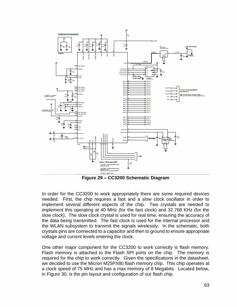
63
Figure 29 – CC3200 Schematic Diagram
In order for the CC3200 to work appropriately there are some required devices needed. First, the chip requires a fast and a slow clock oscillator in order to implement several different aspects of the chip. Two crystals are needed to implement this operating at 40 MHz (for the fast clock) and 32.768 KHz (for the slow clock). The slow clock crystal is used for real time, ensuring the accuracy of the data being transmitted. The fast clock is used for the internal processor and the WLAN subsystem to transmit the signals wirelessly. In the schematic, both crystals pins are connected to a capacitor and then to ground to ensure appropriate voltage and current levels entering the clock. One other major component for the CC3200 to work correctly is flash memory. Flash memory is attached to the Flash SPI ports on the chip. The memory is required for the chip to work correctly. Given the specifications in the datasheet, we decided to use the Micron M25PX80 flash memory chip. This chip operates at a clock speed of 75 MHz and has a max memory of 8 Megabits. Located below, in Figure 30, is the pin layout and configuration of our flash chip.
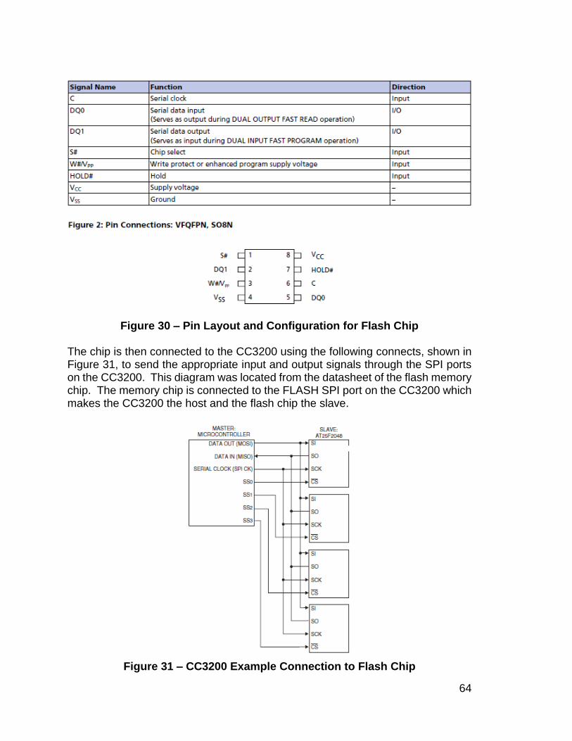
64
Figure 30 – Pin Layout and Configuration for Flash Chip
The chip is then connected to the CC3200 using the following connects, shown in Figure 31, to send the appropriate input and output signals through the SPI ports on the CC3200. This diagram was located from the datasheet of the flash memory chip. The memory chip is connected to the FLASH SPI port on the CC3200 which makes the CC3200 the host and the flash chip the slave.
Figure 31 – CC3200 Example Connection to Flash Chip
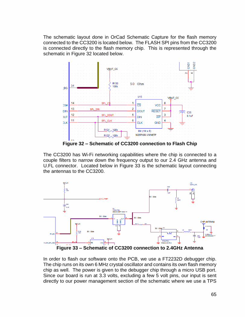
65
The schematic layout done in OrCad Schematic Capture for the flash memory connected to the CC3200 is located below. The FLASH SPI pins from the CC3200 is connected directly to the flash memory chip. This is represented through the schematic in Figure 32 located below.
Figure 32 – Schematic of CC3200 connection to Flash Chip
The CC3200 has Wi-Fi networking capabilities where the chip is connected to a couple filters to narrow down the frequency output to our 2.4 GHz antenna and U.FL connector. Located below in Figure 33 is the schematic layout connecting the antennas to the CC3200.
Figure 33 – Schematic of CC3200 connection to 2.4GHz Antenna
In order to flash our software onto the PCB, we use a FT2232D debugger chip. The chip runs on its own 6 MHz crystal oscillator and contains its own flash memory chip as well. The power is given to the debugger chip through a micro USB port. Since our board is run at 3.3 volts, excluding a few 5 volt pins, our input is sent directly to our power management section of the schematic where we use a TPS

66
voltage regulator to drop down the voltage. Figure 34Figure 35 Figure 1 Figure 35 represent the schematic used to implement these concepts.
Figure 34 – Schematic of FT2232D Debugger Chip
Figure 35 – Schematic of Power Management
4.7.2 Board Layout Once the schematic diagram for the entire PCB was completed, a board layout was generated through PCB Editor. This is done by placing all of the components on a sheet and strategically placing and rotating them in order to shorten wire traces. If done incorrectly, routing the wires to each component will be difficult and/or impossible. PCB Editor has the capability to AutoRoute the traces for all of the lines in the PCB. To do this, all of the parts needed for the board are laid out and connected together automatically. There existed several errors where certain pins and components were not connected to the correct power pins or ground. To fix these issues, we manually went through the board and checked to see if everything was correct. The errors that we found were fixed primarily by either moving objects around or adding extra Vias in order to connect to either Vcc or ground easier. The final board layout is shown in Figure 36 below.
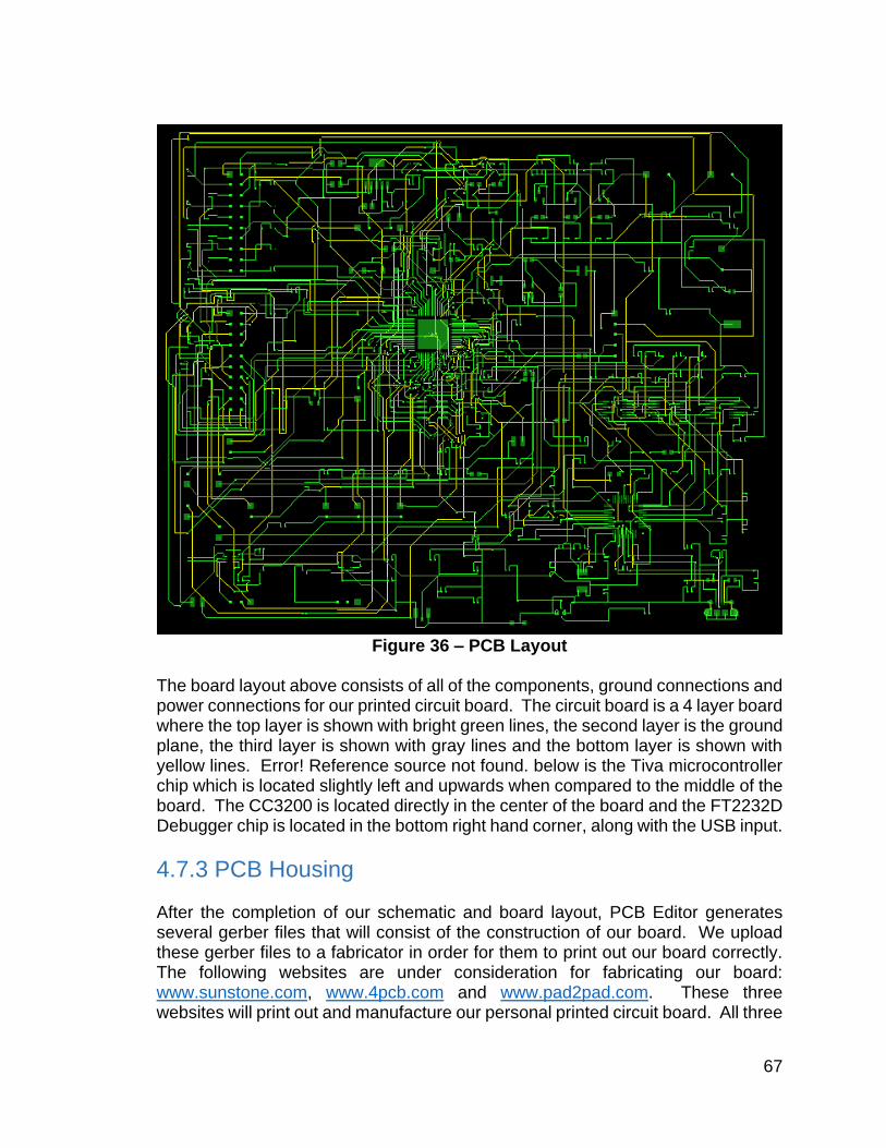
67
Figure 36 – PCB Layout
The board layout above consists of all of the components, ground connections and power connections for our printed circuit board. The circuit board is a 4 layer board where the top layer is shown with bright green lines, the second layer is the ground plane, the third layer is shown with gray lines and the bottom layer is shown with yellow lines. Error! Reference source not found. below is the Tiva microcontroller chip which is located slightly left and upwards when compared to the middle of the board. The CC3200 is located directly in the center of the board and the FT2232D Debugger chip is located in the bottom right hand corner, along with the USB input.
4.7.3 PCB Housing After the completion of our schematic and board layout, PCB Editor generates several gerber files that will consist of the construction of our board. We upload these gerber files to a fabricator in order for them to print out our board correctly. The following websites are under consideration for fabricating our board: www.sunstone.com, www.4pcb.com and www.pad2pad.com. These three websites will print out and manufacture our personal printed circuit board. All three

68
websites will accept the gerber files that PCB Editor produces. Table 16 located below compares the three websites.
Table 16 – PCB Price Comparison
Protocol Sunstone 4PCB Pad2Pad
Single Layer Price $453.25 $33 -
Double Layer Price $463.25 $66 $169.18
Multi-Layer Price $487.39 - $403.08
Gerber Files Accepted Yes Yes Yes
Gerber Files Examination No Yes No
Printing Duration 3 Weeks 3 Weeks 11 Days
After consideration, and budget constraints, we decided to print out our PCB with Advanced Circuits (www.4pcb.com). We were able to finish the design of the board quick enough that the 3 week turnaround time was sufficient for our project. Advanced Circuits was also the cheapest option due to an outstanding student discount.
4.8 Wireless Communication The group has decided to work with the CC3200 microcontroller, in order to add wireless communication to the processor in one integrated package. This chip supports a Wi-Fi connection solution for MCU applications. The CC3200 is a low-power MCU that has Wi-Fi Internet-On-a-Chip capability. While Wi-Fi was not our first choice for wireless communication, the CC3200 allows easy integration into the system while still supporting a strong enough signal to the user. Table 17 below shows the CC3200 chips specifications.
69
Table 17 – CC3200 Specifications
Protocol 802.11b/g/n
Wi-Fi Features STA, AP, Wi-Fi Direct Mode, SmartConfig
Max Throughput 16 Mbps (UDP) & 12 Mbps (TCP)
RX Current 53 mA
TX Current 223 mA
Output Power 18 dBM
The CC3200 chip requires a U.FL antenna to broadcast the signal to the user interface. U.FL cables work with Wi-Fi, Bluetooth and ZigBee so any solution for wireless communications that we decided to use would have incorporated a U.FL cable. These connectors operate on a 2.4 GHz band. A U.FL cable is a mini coaxial cable used for high RF signals. The male end of the cable will be mounted onto the PCB we designed for the system. The female end of the wire is located at the end of the coaxial cable. At the end of the U.FL cable, an antenna is then attached to physically broadcast the signal to the desired location.
4.9 External Interface The CC3200 microcontroller already implements a network processor capable of utilizing the entire TCP/IP stack in a single chip. The main advantage of this software architecture is that it makes implementation of additional features and tasks easy since each task is independent and modular. Also since every task has a common communication point it is easy to send information between tasks. This is especially important for the external communication task because it can modify and potentially request information from every task. As this is an optional feature (aside from the ability to remotely disable the laser) we will not spend much time on its design. In terms of actual develop for the external interface, we will ensure the ability to disable the laser and stop the main task of AIR-STRIKE at any time. These are for safety purposes primarily. As an extension to this we aim to develop more capabilities for commanding AIR-STRIKE from afar. The two platforms we aim to provide direct support for are Windows PCs and Android devices. Aside from this direct support, the system will host a webserver which will allow any device with Wi-Fi capabilities and an internet browser to issue commands.

70
4.10 Power Management For our entire project, all of our components run at 5 volts. This made developing a power supply PCB very simple. We started off with a barrel jack input, where the 120 VAC voltage from a wall outlet is converted to a 5 VDC signal. The input is then sent to many pin headers where our subsystems will connect too. We also created a separate pin header section where the ground of the input is tied to these headers so that all of our subsystems have a common ground and no shorts will be made. Our current driver and both of our servos obtain PWM signals from the MCU in order to communicate. The PWM signals from the MCU are sent at 3.3 volts, however, our subsystems need the signals to be 5 volts. To increase the voltage, we first implement a voltage regulator where the voltage from the input will be stepped down to 3.3 volts. Then through a transistor circuit, we convert the 3.3 volt PWM signal to 5 volts. The transistor acts as a switch and closes the circuit when the PWM signal is read. Located in Figure 37 is our schematic for our power supply voltage.
Figure 37 – Power Supply Schematic
Our design for this PCB was done through Eagle. Figure 38, below, represents our board layout. For this board, we used a 2 layer board where the red and blue sections represent the ground planes.
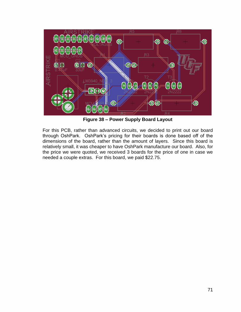
71
Figure 38 – Power Supply Board Layout
For this PCB, rather than advanced circuits, we decided to print out our board through OshPark. OshPark’s pricing for their boards is done based off of the dimensions of the board, rather than the amount of layers. Since this board is relatively small, it was cheaper to have OshPark manufacture our board. Also, for the price we were quoted, we received 3 boards for the price of one in case we needed a couple extras. For this board, we paid $22.75.

72
5.0 Design Summary AIR-STRIKE is an automated anti-air turret which uses a directed energy weapon system in order to neutralize targets. The design was focused around guiding our laser weaponry to a target identified in image attained from our chosen cameras. A microcontroller will handle communication between the devices and send instructions to a gimbal system, which holds the laser, based upon the target’s location. While control is autonomous, methods of control will be offered via Wi-Fi. The primary method will be via Wi-Fi as our system will host a web server that can be connected to. This web server will host a website with options to alter the operation of AIR-STRIKE. We intend to use an outlet to provide AC power to the device. Our chosen microcontroller is the CC3200. We chose this primarily due to the number of ports, its integrated Wi-Fi support, and our understanding that its power will be sufficient for our processing needs. The only computations performed should be minor coordinate transformations in order to translate the target locations into angles that the laser can be directed towards. The primary purpose of the network part of the system is control of and communication between the other subsystems. Communication will be done with byte encoded messages. In our design the primary image processing will be handled by the camera hardware and software itself. The chosen camera, the Pixy (also known as the CMUCam5), contains the capabilities to identify hundreds of potential targets based upon calibrations done ahead of time. It sends a list of these targets locations to the microcontroller. We decided to use two Pixy’s in order to attain wider field of view. This has the added complication of managing two cameras and interpreting their pixel locations in comparison to one another, but we accept this challenge as worthy of the end result. Both will connect to the main PCB via SPI. The directed energy subsystem will contain a gimbal system and a laser. The gimbal will be constructed using an MG90s servo for elevational movement and an another MG90s servo for azimuthal movement. The laser itself will be composed of a S06J laser diode, a Flexmod P3 Driver and lens system from LightPath Technologies. These choices were made to provide us efficient modulation of power and enough max output power to burst a balloon with the beam of our laser.
The software package to be deployed on the CC3200 will be composed of four primary sections. These sections also double as the tasks to be performed. These sections are Watchdog, SimpleLink, Targeting, and HTTP/WebSocket server. Each task communicates with a different physical component and as functions to support said communication. All tasks are run on their own thread and processor resources are managed by FREE-RTOS.

73
Target Acquisition, represented by the Camera_Interface class and containing the Target structure, is where we acquire our targets and send their positions to the rest of the system. It interfaces with the Image Capture subsystem and handles messages to and from the cameras. Turret Movement, represented by the Gimbal_Interface class, handles all commands to move the gimbal and can tell us the current orientation of the gimbal system. It also contains functionality to convert coordinates from the cameras to angles that can be used to guide the laser. Fire Control, represented by the Laser_Interface class, merely allows us to modulate the power of the laser and turn it off and on. Finally, External Communication, represented by the External_Interface class, provides us functionality to communicate with outside devices. This is where we initialize the webserver, Bluetooth, and USB systems and handle any commands and requests. AIR-STRIKE will be cost efficient, light weight, and small with a cylindrical shape to it and the primary components mounted on top. Ports will be available for interfacing and if needed there will also be an external antenna. Further additions, if time permits and resources are available, would be various status lights and buttons on the physical device for operation. Overall, the system is not overly complicated with all roles snuggly filled by the chosen components.

74
6.0 Prototype Integration Each subsystem described in this document will be integrated together to form our overall product. Within this section, we will describe our plan on how we will integrate each subsystem. This process is important to take careful consideration and planning into in order to confirm that our parts will work simultaneously. For our PCB integration, we must analyze and confirm that when connecting external parts to our board, we will not burn out components on the board by applying to much voltage and current.
6.1 Parts Acquisition and Cost For each subsystem in our overall product, several components and parts will be purchased. All of our products will either be purchased online from vendors, or will have already been owned by one of the four team members. The cost of each part will be then be accumulated and put into our budget later on in this report. Each subsystem will have its own sum of materials which those values will then be accumulated into the budget.
6.1.1 PCB Materials For our printed circuit board, we will be uploading our gerber files (the final files generated by eagle cad with our board layout and requirements) to www.4pbc.com. They will be fabricating and assembling our PCB and shipping it to the university. This fabricating company offers student discounts on senior design projects to help lessen the cost of the PCB. This is one main reason why we plan on using www.4pcb.com to build our PCB. This company also has a software that will examine our overall PCB design to confirm that there are no errors within the board layout or schematic diagrams. These two factors were the main ones that caused us to choose 4pcb to be our manufacturer for our project. A 2 layer PCB will cost $33 and a 4 layer PCB will cost $66. For multi-layered designs, a quote must be obtained by contacting the company who offers a 50% discount to students for multi-layered PCBs. For our design, we will need a multi-layered PCB due to the three chips and the other large components involved in our design. Because each multi-layered PCB is priced differently with our fabricator, an exact quote cannot be given to us until we upload our official gerber files. We estimate our cost for the printing of the board, and the service to be roughly $150. We expect to receive the PCB roughly 2-3 weeks after we place our order.
6.1.1.1 PCB Bill of Materials After completing the PCB schematic and the board layout, the next step is to
create a bill of materials for the board including all of the chips, resistors,

75
capacitors, inductors etc. The approximate value of each circuit element can
either be found on google or through the Eagle Cad Design Link. The Design
Link is a strategy where the user enters in keywords of the component that you
want to purchase and Eagle searches its libraries to find the correct parts.
Certain Texas Instruments parts (such as the three TI chips used on the PCB)
are not in the Eagle libraries and must be located online, primarily from the
manufacturer’s website.
Table 18 below is our bill of materials for our PCB.
Table 18 – PCB Bill of Materials
Part Value Size Quantity Price/Unit Total Cost
Capacitor 1.0 pF USC_0402 1 $0.814 $0.81
Capacitor 6.2 pF USC_0402 2 $0.120 $0.24
Capacitor 10 pF USC_0402 2 $0.014 $0.03
Capacitor 12 pF USC_0402 6 $0.020 $0.12
Capacitor 1000 pF USC_0402 1 $0.120 $0.12
Capacitor 3300 pF USC_0402 2 $0.110 $0.22
Capacitor 4700 pF USC_0402 1 $0.091 $0.09
Capacitor 0.1 uF USC_0402 36 $0.118 $4.25
Capacitor 1.0 uF USC_0402 3 $0.240 $0.72
Capacitor 2.2 uF USC_0402 3 $0.330 $0.99
Capacitor 4.7 uF USC_0402 6 $0.350 $2.10
Capacitor 10 uF USC_0402 2 $0.385 $0.77
Capacitor 22 uF USC_0402 2 $0.074 $0.15
LED - LED_0603 5 $0.320 $1.60
Holes - Hole_3.2 3 $- $-
Flash Mem AT25P - 1 $0.508 $0.51
Antenna - - 1 $4.950 $4.95
Jumpers - 2x3 1 $1.160 $1.16
Jumpers - 1x2 2 $0.870 $1.74
Jumpers - 2x2 2 $1.030 $2.06
Inductor 3.6 nH US_0204/5 1 $0.200 $0.20
Inductor 1 uH US_0204/5 1 $0.102 $0.10
Inductor 2.2 uH US_0204/5 2 $0.186 $0.37
Crystal 40 MHz 68SMX 1 $5.920 $5.92
Crystal 32.768 KHz 68SMX 1 $1.500 $1.50
Resistor 0 US_R0402 13 $0.006 $0.07
Resistor 50 6 $0.048 $0.29
Resistor 75 US_R0402 4 $0.001 $0.00
Resistor 100 US_R0402 2 $0.011 $0.02
Resistor 330 US_R0402 5 $0.072 $0.36
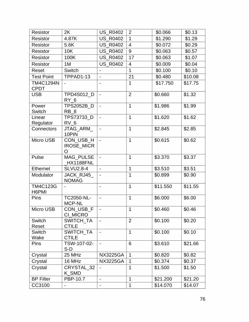
76
Resistor 2K US_R0402 2 $0.066 $0.13
Resistor 4.87K US_R0402 1 $1.290 $1.29
Resistor 5.6K US_R0402 4 $0.072 $0.29
Resistor 10K US_R0402 9 $0.063 $0.57
Resistor 100K US_R0402 17 $0.063 $1.07
Resistor 1M US_R0402 4 $0.009 $0.04
Reset Switch - 1 $0.100 $0.10
Test Point TPPAD1-13 - 21 $0.480 $10.08
TM4C1294NCPDT
- - 1 $17.750 $17.75
USB TPD4S012_DRY_6
- 2 $0.660 $1.32
Power Switch
TPS2052B_DRB_8
- 1 $1.986 $1.99
Linear Regulator
TPS73733_DRV_6
- 1 $1.620 $1.62
Connectors JTAG_ARM_10PIN
- 1 $2.845 $2.85
Micro USB CON_USB_HIROSE_MICRO
- 1 $0.615 $0.62
Pulse MAG_PULSE_HX1188FNL
- 1 $3.370 $3.37
Ethernet SLVU2.8-4 - 1 $3.510 $3.51
Modulator JACK_RJ45_NOMAG
- 1 $0.899 $0.90
TM4C123GH6PMI
- - 1 $11.550 $11.55
Pins TC2050-NL-MCP-NL
- 1 $6.000 $6.00
Micro USB CON_USB_FCI_MICRO
- 1 $0.460 $0.46
Switch Reset
SWITCH_TACTILE
- 2 $0.100 $0.20
Switch Wake
SWITCH_TACTILE
- 1 $0.100 $0.10
Pins TSW-107-02-S-D
- 6 $3.610 $21.66
Crystal 25 MHz NX3225GA 1 $0.820 $0.82
Crystal 16 MHz NX3225GA 1 $0.374 $0.37
Crystal CRYSTAL_32K_SMD
- 1 $1.500 $1.50
BP Filter PBP-10.7 - 1 $21.200 $21.20
CC3100 - - 1 $14.070 $14.07
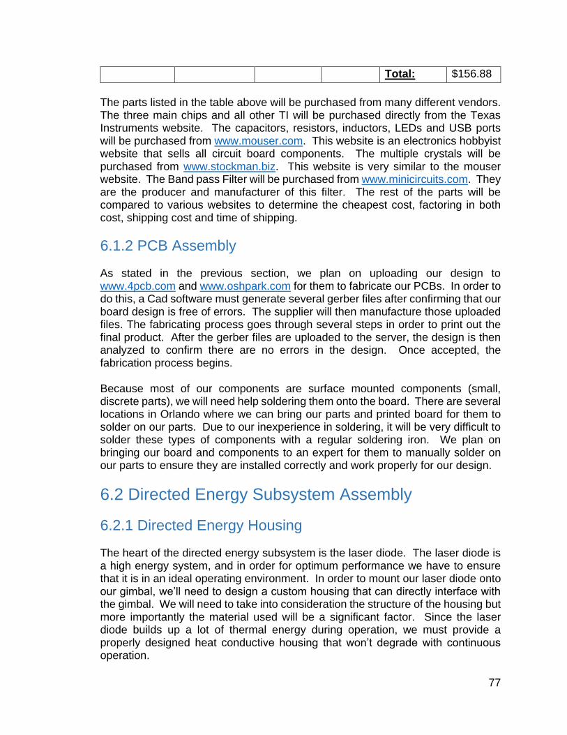
77
Total: $156.88
The parts listed in the table above will be purchased from many different vendors. The three main chips and all other TI will be purchased directly from the Texas Instruments website. The capacitors, resistors, inductors, LEDs and USB ports will be purchased from www.mouser.com. This website is an electronics hobbyist website that sells all circuit board components. The multiple crystals will be purchased from www.stockman.biz. This website is very similar to the mouser website. The Band pass Filter will be purchased from www.minicircuits.com. They are the producer and manufacturer of this filter. The rest of the parts will be compared to various websites to determine the cheapest cost, factoring in both cost, shipping cost and time of shipping.
6.1.2 PCB Assembly As stated in the previous section, we plan on uploading our design to www.4pcb.com and www.oshpark.com for them to fabricate our PCBs. In order to do this, a Cad software must generate several gerber files after confirming that our board design is free of errors. The supplier will then manufacture those uploaded files. The fabricating process goes through several steps in order to print out the final product. After the gerber files are uploaded to the server, the design is then analyzed to confirm there are no errors in the design. Once accepted, the fabrication process begins. Because most of our components are surface mounted components (small, discrete parts), we will need help soldering them onto the board. There are several locations in Orlando where we can bring our parts and printed board for them to solder on our parts. Due to our inexperience in soldering, it will be very difficult to solder these types of components with a regular soldering iron. We plan on bringing our board and components to an expert for them to manually solder on our parts to ensure they are installed correctly and work properly for our design.
6.2 Directed Energy Subsystem Assembly
6.2.1 Directed Energy Housing The heart of the directed energy subsystem is the laser diode. The laser diode is a high energy system, and in order for optimum performance we have to ensure that it is in an ideal operating environment. In order to mount our laser diode onto our gimbal, we’ll need to design a custom housing that can directly interface with the gimbal. We will need to take into consideration the structure of the housing but more importantly the material used will be a significant factor. Since the laser diode builds up a lot of thermal energy during operation, we must provide a properly designed heat conductive housing that won’t degrade with continuous operation.

78
The most inexpensive material we can use is wood. We can use woodshop machinery to shape the housing to proper dimensions at very minimal cost. The downside to using wood is that it has very poor thermal properties. The surface may begin to char or even catch on fire after repeated exposure to thermal stress. Another proposed idea was to use metal rods to hold the laser diode in place on the gimbal. The purpose of this is to minimize material contact with the laser diode so the heat generated can dispel into the air rather than relying on a thermal conductive material to dissipate it. This design will require extra measures to ensure the diode is stable as the gimbal rotates to align with the target or else the diode may become loose and fire the beam at an unintended target. Another material we considered for a laser diode housing is aluminum. Aluminum is widely used in industry as a heat sink material because of its high thermal conductivity. Aluminum is relatively low cost and a block can be constructed by using CNC processes or other machinery. CNC machines are very efficient for small, simple design and take in a standard CAD model. One downside to aluminum is that it is mechanically soft, meaning under high thermal loads the structure may warp. However, at our operating temperatures we will probably not experience any issues. Recently, thermoplastics have received a lot of attention, specifically polycarbonate. Polycarbonates are used in a wide range of applications from the medical field to the electrical and aerospace industry. It exhibits very strong mechanical properties that allow it to be easily molded without cracking or breaking. Polycarbonate also has very strong thermal resistance. It has a glass transition temperature of around 300°F, so that a thermal stresses below this the material will not weaken. This is well above the range of our laser diodes operating temperatures. Table 19 shows many of the thermal and mechanical properties of polycarbonate. To get a good idea of the response of the polycarbonate while under a repeated thermal load, a heat analysis will be simulated using Finite Difference software. The material properties will be defined with the table below. Another benefit is that polycarbonate is used in 3D additive printing, so we can easily import a CAD model and create the design using UCFs laser printing lab. Notice, that polycarbonate combined with glass filling offers greater structural strength. For our applications, we will most likely not need the extra strength since the load will be light.

79
Table 19 – Properties of Polycarbonate
(Permission given by Boedeker Plastics, Inc)
6.2.2 Simulation for Housing using Finite Difference Model In order to ensure that the laser diode housing is able to withstand the thermal energy generated by the diode, we will carry out simulations using finite difference software to model how the material will respond. The finite difference method is a well-recognized technique in electromagnetic analysis. It’s a numerical method that attempts to solve differential equations using finite elements over a given geometry. The finite difference method in heat transfer is used to solve the heat equation given by,
𝜕𝑢
𝜕𝑡− 𝛼∇2𝑢 = 0
where α is the thermal diffusivity, u is a function of x,y, and z coordinate space defining the temperature and ∇ is the Laplace operator. This standard differential equation is solved over a discrete series of finite elements to obtain an approximate solution. A simple one dimensional equation is iterated over a series of explicitly defined steps to solve for heat transfer. Figure 39 shows an example of the steps to be iterated over in the one dimensional case.
Figure 39 – One dimensional space divided into evenly spaced segments, where j is taken to be the center point. The variable j represents the spatial
coordinate and n represents the temporal step.

80
When solving the iterations, we break up the differential equation shown in equation 1 into steps in the time and spatial domain. The representation of the temperature variable would have the form given in the equation below.
𝑢(𝑥𝑗 , 𝑡𝑛) = 𝑢𝑗𝑛
Now, the finite difference method will break up the differential equation into steps and solve for the next element in the array by using the solution set from the previous element. Boundary conditions play a major role in initiating the loop so that the software can know how to treat the first and last elements of the geometry. The basic layout of iterations that the software attempts to solve is given in equation the equation below,
𝑢𝑗𝑛+1 = 𝑢𝑗+1
𝑛 − 𝑢𝑗𝑛
This equation shows how the next time step is solved by using the current working element and the next working element. The boundary conditions can be defined as perfectly absorbing layers or as transparent layers. The former will restrict heat flow from one domain to another, while the latter will allow heat to travel across into the next geometry. It’s crucial to properly assign the boundary conditions for the most accurate results. The step size is also an important parameter in gaining accuracy of the simulation. The larger the step size, the less accurate the result for the differential equation will be. There is a tradeoff when minimizing the step size. Large geometries with a small element size can take up a lot of memory space that many computers cannot handle. Generally, when carrying out finite difference method in the professional workplace, a computer with high RAM storage is required for accurate results. In the three dimensional case, the system of equations become more and more complex. This is because the geometry of the elements is more elaborate. In general, when solving over a three dimensional structure, the software uses a triangular mesh, yet it is not uncommon to find yourself using hexagonal meshes are other n-sided polygons. When using a polygon with more sides, the system of equations becomes a larger memory load on the computer. In our simulations, we will use a triangular mesh that is approximately a one-thousandth of the size of the laser housing. This is the optimal balance for accuracy and computer memory space for the computer we will be using. The software used to carry out the thermal analysis is Comsol Multiphysics v4.2. This software has full capabilities for carrying out RF/microwave, optical, opto-acoustic, mechanical and thermal analysis. The software has a built in material library where each material has experimentally confirmed thermal, mechanical and

81
electrical properties. In our simulation, we will use the copper material which as the material properties shown in Table 20.
Table 20 – Properties of Copper as given by Comsol’s material library
The geometry of the simulation will be a simple heat source given as a cylindrical shape that will represent the diode. During operation, the maximum heat it will give off is approximately 60°C so our simulations will be based off that heat source temperature. The housing will be modeled as a simple rectangular structure to observe how the heat radiates outward from the laser diode. Based on how deep the heat propagates into the housing material, we can choose to remove some of the material to further reduce cost of the housing. The first simulation we will run will be with polycarbonate material. Comsol will allow us to enter a new material with defined properties, so the simulation will be run with the properties given in Table 20. There is also a simulated layer of thermal grease. We will apply this to the diode module to serve as an additional thermally conductive layer and as an interface between the housing and diode for further mechanical bond strength. As previously mentioned, choosing the proper mesh size is very important. Comsol allows the user to explicitly define the size of the mesh or you can use the built in mesh that can range from ‘extremely fine’ to ‘extremely coarse’. We will define a mesh at one-thousandth of the length of the housing, as shown below in Figure 40.
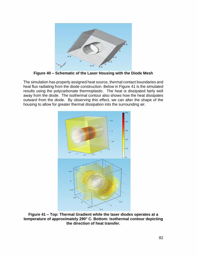
82
Figure 40 – Schematic of the Laser Housing with the Diode Mesh
The simulation has properly assigned heat source, thermal contact boundaries and heat flux radiating from the diode construction. Below in Figure 41 is the simulated results using the polycarbonate thermoplastic. The heat is dissipated fairly well away from the diode. The isothermal contour also shows how the heat dissipates outward from the diode. By observing this effect, we can alter the shape of the housing to allow for greater thermal dissipation into the surrounding air.
Figure 41 – Top: Thermal Gradient while the laser diodes operates at a
temperature of approximately 290° C. Bottom: Isothermal contour depicting the direction of heat transfer.
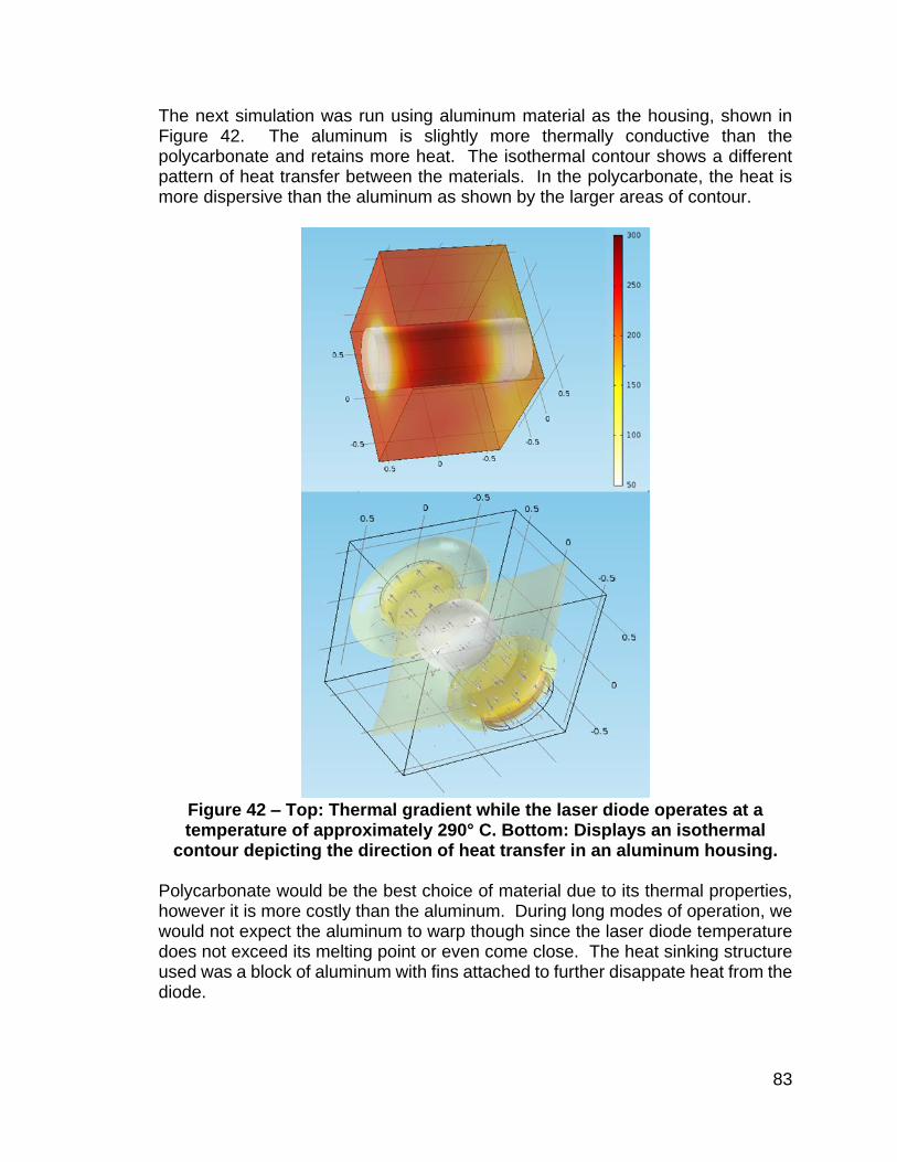
83
The next simulation was run using aluminum material as the housing, shown in Figure 42. The aluminum is slightly more thermally conductive than the polycarbonate and retains more heat. The isothermal contour shows a different pattern of heat transfer between the materials. In the polycarbonate, the heat is more dispersive than the aluminum as shown by the larger areas of contour.
Figure 42 – Top: Thermal gradient while the laser diode operates at a temperature of approximately 290° C. Bottom: Displays an isothermal
contour depicting the direction of heat transfer in an aluminum housing. Polycarbonate would be the best choice of material due to its thermal properties, however it is more costly than the aluminum. During long modes of operation, we would not expect the aluminum to warp though since the laser diode temperature does not exceed its melting point or even come close. The heat sinking structure used was a block of aluminum with fins attached to further disappate heat from the diode.
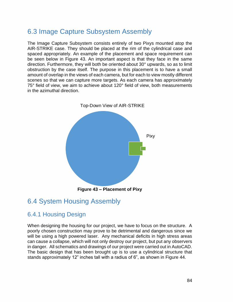
84
6.3 Image Capture Subsystem Assembly The Image Capture Subsystem consists entirely of two Pixys mounted atop the AIR-STRIKE case. They should be placed at the rim of the cylindrical case and spaced appropriately. An example of the placement and space requirement can be seen below in Figure 43. An important aspect is that they face in the same direction. Furthermore, they will both be oriented about 30° upwards, so as to limit obstruction by the case itself. The purpose in this placement is to have a small amount of overlap in the views of each camera, but for each to view mostly different scenes so that we can capture more targets. As each camera has approximately 75° field of view, we aim to achieve about 120° field of view, both measurements in the azimuthal direction.
Top-Down View of AIR-STRIKE
Pixy
Figure 43 – Placement of Pixy
6.4 System Housing Assembly
6.4.1 Housing Design When designing the housing for our project, we have to focus on the structure. A poorly chosen construction may prove to be detrimental and dangerous since we will be using a high powered laser. Any mechanical deficits in high stress areas can cause a collapse, which will not only destroy our project, but put any observers in danger. All schematics and drawings of our project were carried out in AutoCAD. The basic design that has been brought up is to use a cylindrical structure that stands approximately 12” inches tall with a radius of 6”, as shown in Figure 44.
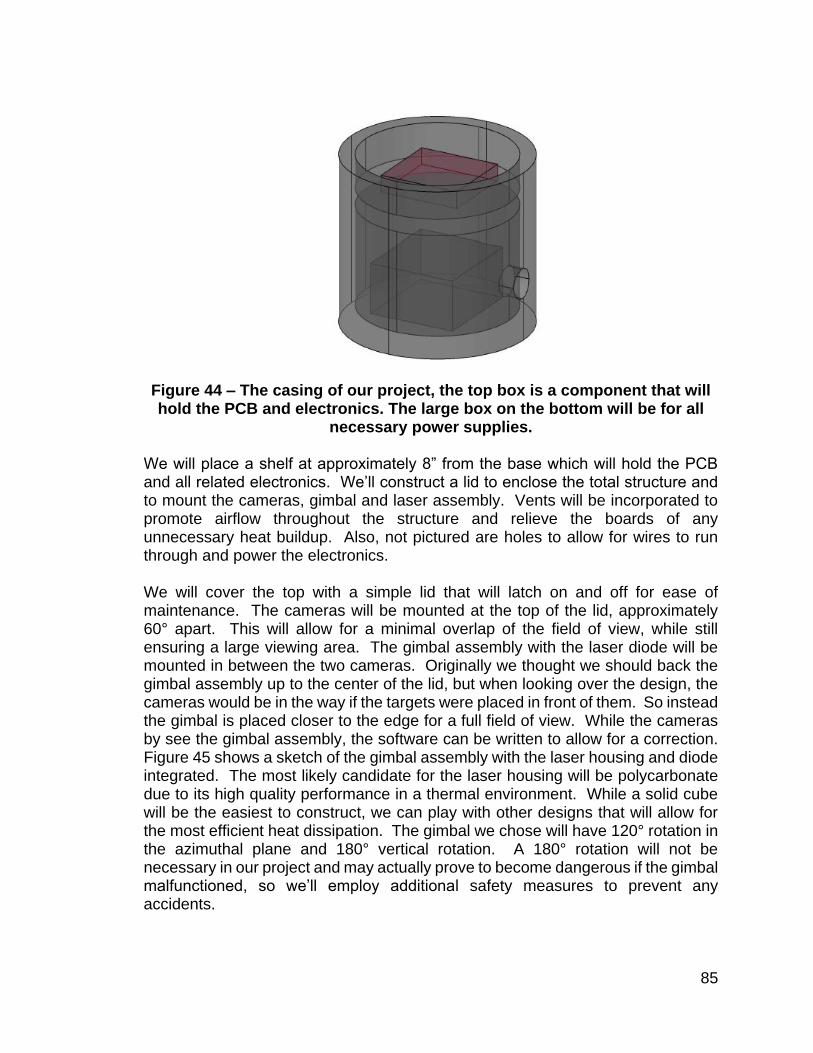
85
Figure 44 – The casing of our project, the top box is a component that will hold the PCB and electronics. The large box on the bottom will be for all
necessary power supplies. We will place a shelf at approximately 8” from the base which will hold the PCB and all related electronics. We’ll construct a lid to enclose the total structure and to mount the cameras, gimbal and laser assembly. Vents will be incorporated to promote airflow throughout the structure and relieve the boards of any unnecessary heat buildup. Also, not pictured are holes to allow for wires to run through and power the electronics. We will cover the top with a simple lid that will latch on and off for ease of maintenance. The cameras will be mounted at the top of the lid, approximately 60° apart. This will allow for a minimal overlap of the field of view, while still ensuring a large viewing area. The gimbal assembly with the laser diode will be mounted in between the two cameras. Originally we thought we should back the gimbal assembly up to the center of the lid, but when looking over the design, the cameras would be in the way if the targets were placed in front of them. So instead the gimbal is placed closer to the edge for a full field of view. While the cameras by see the gimbal assembly, the software can be written to allow for a correction. Figure 45 shows a sketch of the gimbal assembly with the laser housing and diode integrated. The most likely candidate for the laser housing will be polycarbonate due to its high quality performance in a thermal environment. While a solid cube will be the easiest to construct, we can play with other designs that will allow for the most efficient heat dissipation. The gimbal we chose will have 120° rotation in the azimuthal plane and 180° vertical rotation. A 180° rotation will not be necessary in our project and may actually prove to become dangerous if the gimbal malfunctioned, so we’ll employ additional safety measures to prevent any accidents.
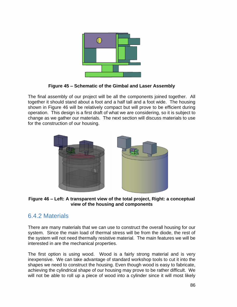
86
Figure 45 – Schematic of the Gimbal and Laser Assembly
The final assembly of our project will be all the components joined together. All together it should stand about a foot and a half tall and a foot wide. The housing shown in Figure 46 will be relatively compact but will prove to be efficient during operation. This design is a first draft of what we are considering, so it is subject to change as we gather our materials. The next section will discuss materials to use for the construction of our housing.
Figure 46 – Left: A transparent view of the total project, Right: a conceptual
view of the housing and components
6.4.2 Materials There are many materials that we can use to construct the overall housing for our system. Since the main load of thermal stress will be from the diode, the rest of the system will not need thermally resistive material. The main features we will be interested in are the mechanical properties. The first option is using wood. Wood is a fairly strong material and is very inexpensive. We can take advantage of standard workshop tools to cut it into the shapes we need to construct the housing. Even though wood is easy to fabricate, achieving the cylindrical shape of our housing may prove to be rather difficult. We will not be able to roll up a piece of wood into a cylinder since it will most likely
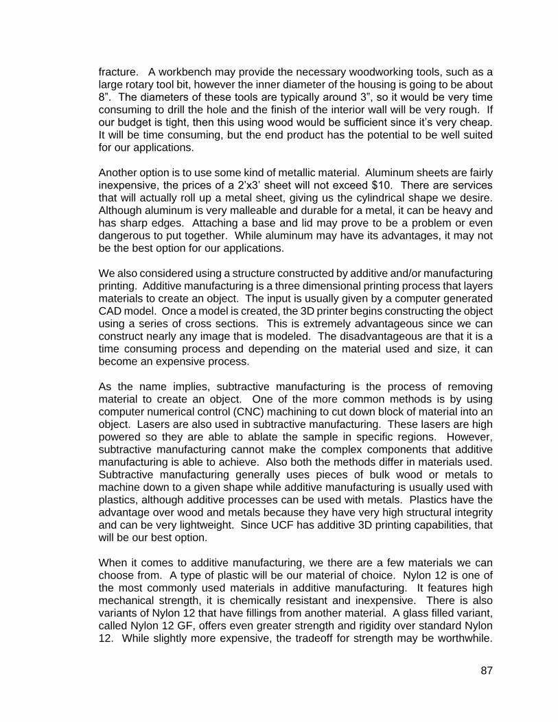
87
fracture. A workbench may provide the necessary woodworking tools, such as a large rotary tool bit, however the inner diameter of the housing is going to be about 8”. The diameters of these tools are typically around 3”, so it would be very time consuming to drill the hole and the finish of the interior wall will be very rough. If our budget is tight, then this using wood would be sufficient since it’s very cheap. It will be time consuming, but the end product has the potential to be well suited for our applications. Another option is to use some kind of metallic material. Aluminum sheets are fairly inexpensive, the prices of a 2’x3’ sheet will not exceed $10. There are services that will actually roll up a metal sheet, giving us the cylindrical shape we desire. Although aluminum is very malleable and durable for a metal, it can be heavy and has sharp edges. Attaching a base and lid may prove to be a problem or even dangerous to put together. While aluminum may have its advantages, it may not be the best option for our applications. We also considered using a structure constructed by additive and/or manufacturing printing. Additive manufacturing is a three dimensional printing process that layers materials to create an object. The input is usually given by a computer generated CAD model. Once a model is created, the 3D printer begins constructing the object using a series of cross sections. This is extremely advantageous since we can construct nearly any image that is modeled. The disadvantageous are that it is a time consuming process and depending on the material used and size, it can become an expensive process. As the name implies, subtractive manufacturing is the process of removing material to create an object. One of the more common methods is by using computer numerical control (CNC) machining to cut down block of material into an object. Lasers are also used in subtractive manufacturing. These lasers are high powered so they are able to ablate the sample in specific regions. However, subtractive manufacturing cannot make the complex components that additive manufacturing is able to achieve. Also both the methods differ in materials used. Subtractive manufacturing generally uses pieces of bulk wood or metals to machine down to a given shape while additive manufacturing is usually used with plastics, although additive processes can be used with metals. Plastics have the advantage over wood and metals because they have very high structural integrity and can be very lightweight. Since UCF has additive 3D printing capabilities, that will be our best option. When it comes to additive manufacturing, we there are a few materials we can choose from. A type of plastic will be our material of choice. Nylon 12 is one of the most commonly used materials in additive manufacturing. It features high mechanical strength, it is chemically resistant and inexpensive. There is also variants of Nylon 12 that have fillings from another material. A glass filled variant, called Nylon 12 GF, offers even greater strength and rigidity over standard Nylon 12. While slightly more expensive, the tradeoff for strength may be worthwhile.
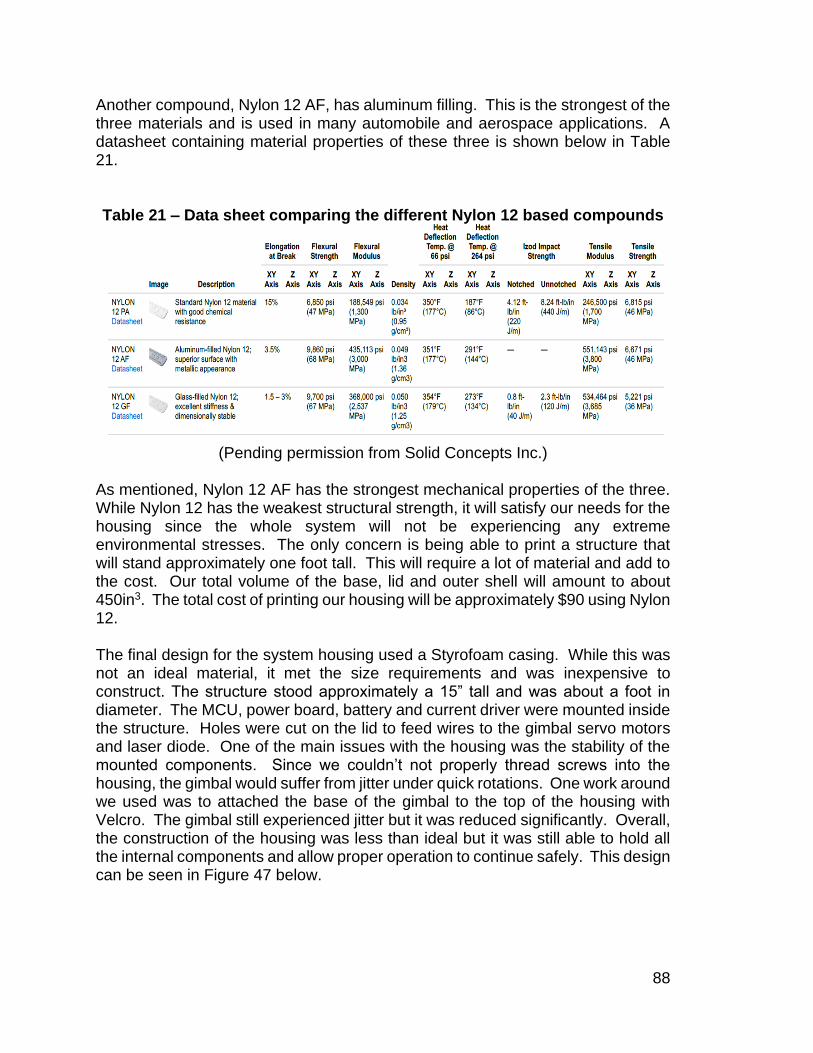
88
Another compound, Nylon 12 AF, has aluminum filling. This is the strongest of the three materials and is used in many automobile and aerospace applications. A datasheet containing material properties of these three is shown below in Table 21. Table 21 – Data sheet comparing the different Nylon 12 based compounds
(Pending permission from Solid Concepts Inc.)
As mentioned, Nylon 12 AF has the strongest mechanical properties of the three. While Nylon 12 has the weakest structural strength, it will satisfy our needs for the housing since the whole system will not be experiencing any extreme environmental stresses. The only concern is being able to print a structure that will stand approximately one foot tall. This will require a lot of material and add to the cost. Our total volume of the base, lid and outer shell will amount to about 450in3. The total cost of printing our housing will be approximately $90 using Nylon 12. The final design for the system housing used a Styrofoam casing. While this was not an ideal material, it met the size requirements and was inexpensive to construct. The structure stood approximately a 15” tall and was about a foot in diameter. The MCU, power board, battery and current driver were mounted inside the structure. Holes were cut on the lid to feed wires to the gimbal servo motors and laser diode. One of the main issues with the housing was the stability of the mounted components. Since we couldn’t not properly thread screws into the housing, the gimbal would suffer from jitter under quick rotations. One work around we used was to attached the base of the gimbal to the top of the housing with Velcro. The gimbal still experienced jitter but it was reduced significantly. Overall, the construction of the housing was less than ideal but it was still able to hold all the internal components and allow proper operation to continue safely. This design can be seen in Figure 47 below.
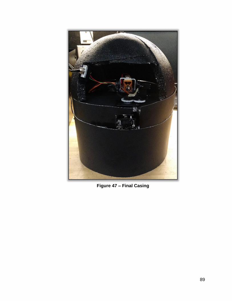
89
Figure 47 – Final Casing

90
7.0 Test Plan Our targeting system will go through a vast amount of tests in order to confirm that it works appropriately. These tests will range from the system level down to the individual component level. For example, we will be running tests on the camera as its own system and then again after being integrated into the system. Testing each component at all levels of integration is critical in order to confirm that we have the correct components and that those components work as expected. It is much easier to fix issues at a low system level rather than on a fully integrated level. Our software tests will all be conducted on the Launchpad versions of the microcontroller so that we can eliminate any issues found with our designed PCB. Using the Launchpad version of the chips will ensure that all connections (power, ground and GPIO pins) are all connected correctly. We will conduct several unique software tests in order to perfect our codes before integrating them with our designed PCB and final system. Ensuring that our software works correctly and quickly on the ideal boards is critical when integrating all of our subsystems together. This will allow us to locate any issues that we stumble upon after conducting all of our hardware and software subsystem tests. Once all of the subsystems are tested separately, then the overall targeting system will be constructed. The system level testing will then begin where all components will be tested once again after being integrated. This will prove if our system will work all together or not. After conducting all of our system-level tests, our final test procedure will be a dry-run of our final prototype demonstration. This will show that the system can locate, target and track balloon shaped objects and when commanded, the laser can pop the tracked balloon. It is then that we will be able to make our final adjustments to optimize our system.
7.1 Test Environment Due to the uniqueness of this product, we will need many test environments in order to confirm that all subsystems work appropriately. The materials required for successful testing will include: a computer to send the software to the PCB, an android device to transmit fire signals to the laser, balloons to confirm that the laser has a strong enough beam to pop the balloon and safety goggles to protect our eyes from harmful electromagnetic waves.
7.1.1 Generic Testing Location The testing environment for testing the software and the cameras ability to locate, target and track objects can be conducted anywhere. Ideally, the testing conducted on the PCB and the cameras should be done in a lab where multimeters are available. When testing the PCBs abilities initially, having a multimeter will be

91
useful to determine if the appropriate amount of voltage and current are entering and leaving the correct nodes. The actual environment for testing the PCB and the camera should vary. This will be explained in the camera testing section below.
7.1.2 High-Power Laser Testing Location When testing the laser, safety goggles will be required on all participants. When using a Class 3 or Class 4 laser, goggles are required in order to protect our eyes from harmful rays. When testing the laser, when operating in the high powered wattage range, we will be conducting our tests in a closed off lab in the CREOL building. When firing high powered lasers, no doors or windows will be open. All avenues for the laser beam to escape the room must be enclosed. Also, a light outside the lab will be illuminated in order to show that a laser is being fired within the room. This will ensure that no body enters the lab during the testing process. Due to the potentiometer in the laser design, that will limit the lasers power output, we will be able to test the laser in open areas when the output is below the 500 milliwatt level. This is the threshold that classifies our laser as high-powered. When firing at a certain power and wavelength, the laser beam will be eye-safe allowing us to test its capabilities outside of a lab.
7.2 Hardware Unit Test In this section, we will discuss the individual component level testing procedures that we will be conducting. Every component and part must go through its own tests prior to integrating them into the total system in order to confirm that they work beforehand. Testing at the subsystem and component level is just as important as testing at the system level to ensure that all parts work correctly before integrating them together. It is much easier to diagnose issues with subsystems when they are being tested individually rather than as a whole system.
7.2.1 PCB Testing The testing for the PCB will be a detailed procedure to confirm that all parts of the circuit board work correctly. The PCB incorporates several different chips in order to complete the requirements defined in this document. The PCB will contain all of the software for our project, which will be tested in section 7.3. Within this section, test procedures will be provided for the CC3200 and all other components.
7.2.1.1 CC3200 Microcontroller Testing The CC3200 microcontroller will be the primary focus for the PCB testing section. This chip will generate all of the signals that will be sent to the cameras, laser, servos and integrated network processor.

92
Power Test Purpose: To ensure that the microcontroller is receiving the appropriate voltage and current to power on the chip. Procedure:
1. Connect the power supply to the PCB through the USB port. 2. Download code onto the board that will blink an LED when the board is
powered on and has received the program.
Expected Result: After running the code, the designated LED will blink continuously. Correcting errors: If the LED does not power on, it will show us that either the software downloaded onto the chip is incorrect, or the power is not connected correctly. This can be decided by downloading the blinking LED code onto the CC3200 Microcontroller Launchpad that our PCB design is based off of. If the LED blinks on that board, then we can confirm that there is a power issue. Laser and Gimbal Test Purpose: To confirm that appropriate signals are being sent to the servos for the laser gimbal as well as to the laser. The signals to the servos will tell the gimbal where to point and when to move to track the target. The signal sent to the laser will tell the laser when to fire and at what wattage to fire at. Procedure:
1. The servos and laser are connected to the PCB through the Pulse-Width Module (PWM) pins of the microcontroller. We will test the PWM signals the same way we tested the SPI ports and the power.
2. We will write a code that will utilize the PWM pins being used and if accepted, an LED will flash indicating success.
Expected Result: At the conclusion of the code, the LED should be flashing. Correcting Errors: If we fail, we will follow the same procedure as before to determine if it is a hardware or software failure.
7.2.1.2 CC3200 Network Testing The one of the purposes of the CC3200 chip is to wirelessly broadcast signals to the user to determine when to fire the laser. We did not want to make our system autonomous due to the high-powered laser. It would not be a safe system if the laser fired freely. The testing for the CC3200 will determine if the correct power is being sent to the chip and if the chip is broadcasting the signals through a Wi-Fi radio frequency signal.

93
Power Test Purpose: The testing for the CC3200 network processor will be very similar to the testing done for the CC3200 main processor because both are integrated onto the same chip. Procedure:
1. Download code to the board that will utilize the CC3200 network capabilities.
2. Flash network code to the CC3200 and check that the network status LEDs are on.
Expected Result: The network status LEDs should be on to confirm that the CC3200 network processes are running Correcting Errors: For all of the CC3200 tests, we will follow the same procedure as above when we find a failure to determine if we have encountered a software or hardware failure. Broadcasting Test Purpose: To determine if the chip is working correctly, a U.Fl antenna will be connected to the board to help boost the signals. Because we are doing individual component tests, the laser will not be fired to confirm that signals can be transmitted and received from the chip. Rather, we will connect any device, to the PCBs Wi-Fi network and then send a faulty signal to confirm that it was received. Procedure:
1. Connect any external mobile device to the PCB through the CC3200s Wi-Fi network.
2. Download code that will flash one LED when our external device has connected to the network.
3. Send a signal to the external device and blink a second LED. 4. A third LED will then flash when the PCB has received a signal from the
external device.
Expected Result: All three LEDs should be blinking at the conclusion of the code to confirm that all three steps in the code were completed. Correcting Errors: The same procedure will be followed to determine if our errors are hardware or software related.
7.2.1.3 FT2232D Testing

94
While the CC3200 is the main component on the PCB, The FT2232D debugger chip is included in our PCB design in order to make testing easier for our board. This chips sole purpose in the design is to aid in the debugging process for the software downloaded onto the board. For individual testing purposes, we will not test this chip because its objectives do not affect our overall product. The only individual test we will conduct is to ensure that the chip powers on when power is applied to the PCB. As long as the chip turns on, then the individual testing is a success for this test. We will determine if power is applied correctly to the chip by blinking an LED.
7.2.2 Directed Energy Testing Before we are able to integrate the laser diode system into our design, it is essential that we characterize the output beam and ensure that it is in proper working order and within factory specifications. The properties that we will be concerned with are the beam profile, beam divergence, and power output for different input currents. Measuring Beam Profile and Divergence Purpose: The first test of the laser diode involves measurement of the beam after being collimated by the optical lenses. Ideally, our lens would not produce of any type of aberration and result in a perfectly Gaussian single order mode. While such perfect conditions may not be achievable, we can get very close by properly handling the optics and ensuring a good alignment for the diode to the collimating optics. In order to view the beam profile from the laser diode and optics, we must use the proper camera. For this type of application, we will use a charge coupled device or otherwise known as a CCD camera. These devices operate by responding to electrical movement on the capacitor array. These arrays are photoactive, meaning when light is incident on the array surface each capacitor collects an electric charge that is directly proportional to the light intensity. Since our laser will be operating at relatively high power, we have to take additional safety measures to protect the CCD array. To do so, we’ll place the necessary optical density filters to be sure we do not saturate and damage the array. The purpose of viewing the laser diode output beam profile is to ensure that we have a near perfect first order mode. This mode is very closely approximated by a Gaussian function of the form:
𝐼(𝑟, 𝑧) = 𝐼0(𝑤0
𝑤(𝑧))2𝑒
(−2𝑟2
𝑤(𝑧)2)
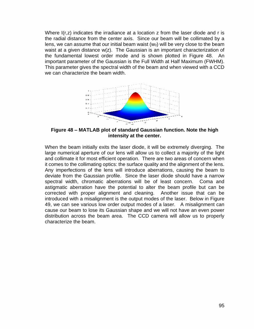
95
Where I(r,z) indicates the irradiance at a location z from the laser diode and r is the radial distance from the center axis. Since our beam will be collimated by a lens, we can assume that our initial beam waist (w0) will be very close to the beam waist at a given distance w(z). The Gaussian is an important characterization of the fundamental lowest order mode and is shown plotted in Figure 48. An important parameter of the Gaussian is the Full Width at Half Maximum (FWHM). This parameter gives the spectral width of the beam and when viewed with a CCD we can characterize the beam width.
Figure 48 – MATLAB plot of standard Gaussian function. Note the high
intensity at the center. When the beam initially exits the laser diode, it will be extremely diverging. The large numerical aperture of our lens will allow us to collect a majority of the light and collimate it for most efficient operation. There are two areas of concern when it comes to the collimating optics: the surface quality and the alignment of the lens. Any imperfections of the lens will introduce aberrations, causing the beam to deviate from the Gaussian profile. Since the laser diode should have a narrow spectral width, chromatic aberrations will be of least concern. Coma and astigmatic aberration have the potential to alter the beam profile but can be corrected with proper alignment and cleaning. Another issue that can be introduced with a misalignment is the output modes of the laser. Below in Figure 49, we can see various low order output modes of a laser. A misalignment can cause our beam to lose its Gaussian shape and we will not have an even power distribution across the beam area. The CCD camera will allow us to properly characterize the beam.
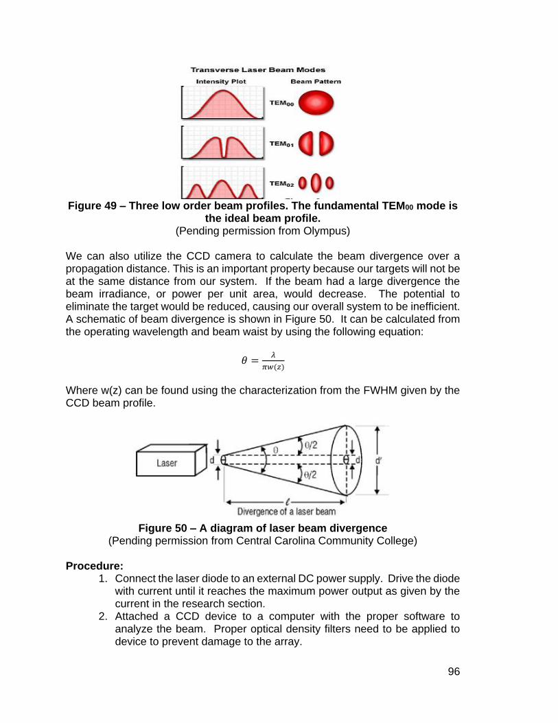
96
Figure 49 – Three low order beam profiles. The fundamental TEM00 mode is
the ideal beam profile. (Pending permission from Olympus)
We can also utilize the CCD camera to calculate the beam divergence over a propagation distance. This is an important property because our targets will not be at the same distance from our system. If the beam had a large divergence the beam irradiance, or power per unit area, would decrease. The potential to eliminate the target would be reduced, causing our overall system to be inefficient. A schematic of beam divergence is shown in Figure 50. It can be calculated from the operating wavelength and beam waist by using the following equation:
𝜃 =𝜆
𝜋𝑤(𝑧)
Where w(z) can be found using the characterization from the FWHM given by the CCD beam profile.
Figure 50 – A diagram of laser beam divergence
(Pending permission from Central Carolina Community College) Procedure:
1. Connect the laser diode to an external DC power supply. Drive the diode with current until it reaches the maximum power output as given by the current in the research section.
2. Attached a CCD device to a computer with the proper software to analyze the beam. Proper optical density filters need to be applied to device to prevent damage to the array.
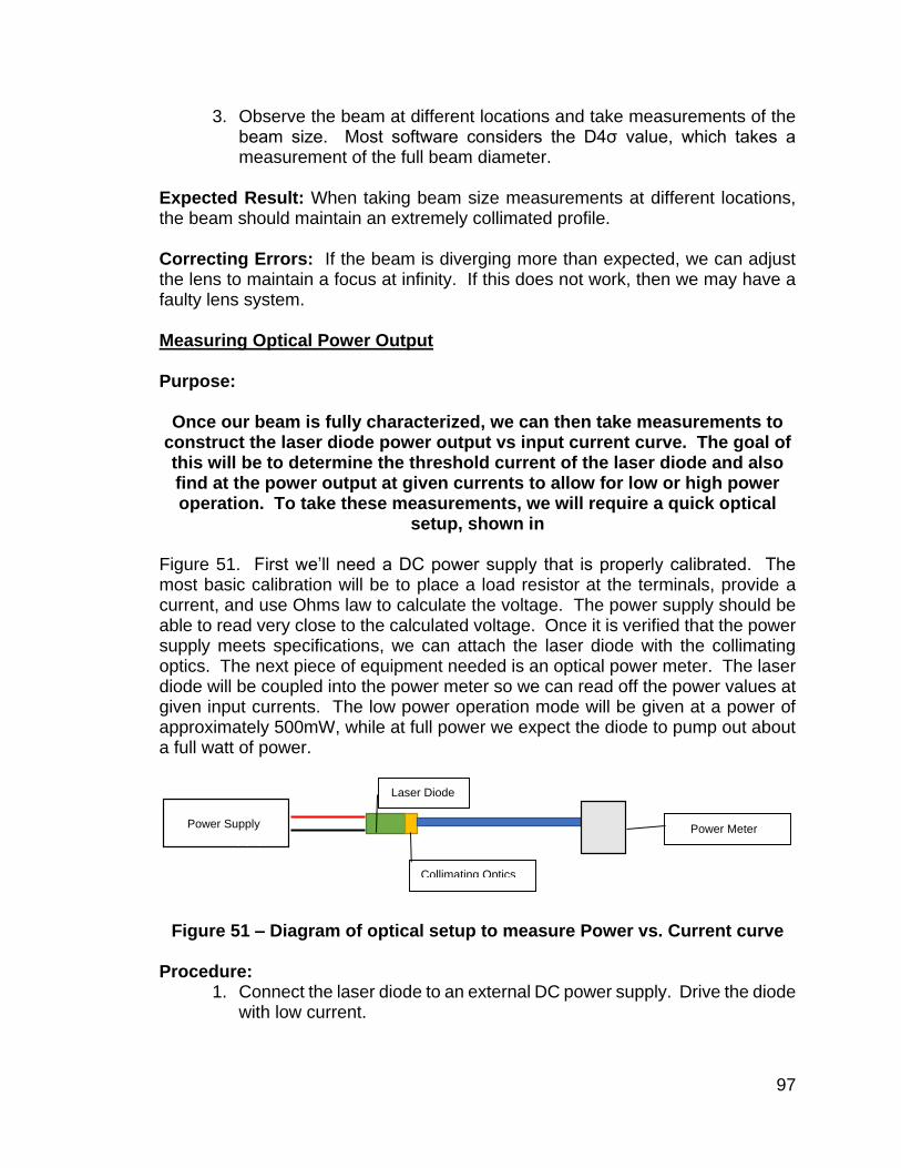
97
3. Observe the beam at different locations and take measurements of the beam size. Most software considers the D4σ value, which takes a measurement of the full beam diameter.
Expected Result: When taking beam size measurements at different locations, the beam should maintain an extremely collimated profile. Correcting Errors: If the beam is diverging more than expected, we can adjust the lens to maintain a focus at infinity. If this does not work, then we may have a faulty lens system. Measuring Optical Power Output Purpose:
Once our beam is fully characterized, we can then take measurements to construct the laser diode power output vs input current curve. The goal of this will be to determine the threshold current of the laser diode and also find at the power output at given currents to allow for low or high power operation. To take these measurements, we will require a quick optical
setup, shown in
Figure 51. First we’ll need a DC power supply that is properly calibrated. The most basic calibration will be to place a load resistor at the terminals, provide a current, and use Ohms law to calculate the voltage. The power supply should be able to read very close to the calculated voltage. Once it is verified that the power supply meets specifications, we can attach the laser diode with the collimating optics. The next piece of equipment needed is an optical power meter. The laser diode will be coupled into the power meter so we can read off the power values at given input currents. The low power operation mode will be given at a power of approximately 500mW, while at full power we expect the diode to pump out about a full watt of power.
Figure 51 – Diagram of optical setup to measure Power vs. Current curve Procedure:
1. Connect the laser diode to an external DC power supply. Drive the diode with low current.
Laser Diode
Collimating Optics
Power Meter Power Supply

98
2. Power on a digital optical power meter and pass the beam through its aperture.
3. Begin to increase the current in intervals of 10mA and record the power at each interval. After many successions, we’ll have the necessary data to construct the optical power vs current curve.
Expected Result: Once the power output reaches a maximum as given in the research section, the diode can be powered down to avoid overpowering it. The gathered data points should be plotted and resemble the same optical power output vs current curve as the specifications. Correcting Errors: The only cause of error is if the laser diode is not functioning properly. There is no practical way to fix the diode if the power output is not as rated. This would indicate the diode may be blown and we will require a new one. Measuring Generated Thermal Energy Purpose: After generating the optical power versus input current curve, we must take into consideration the thermal impact on the laser diode. There is a considerable amount of heat accumulation during long operation and this has an effect on power output. A digital thermal couple is a great tool to monitor heat buildup. By using this we can determine whether the diode continuously heats up or if the heat plateaus off after some time of operation, and if so we can find the time it takes for the diode to heat up to a maximum. Then we can also find the power loss associated with the heated diode. A properly selected heat sink will help dissipate the thermal buildup and allow for maximum output efficiency during operation. Procedure:
1. Connect the laser diode to an external DC power supply. Drive the diode with current until it reaches the maximum power output as determined by the curves in section 3.4.1.
2. Probe the laser diode with a thermal coupler at one minute time intervals to determine its temperature increase over time.
Expected Result: The diode should increase to a specific temperature and then plateau off after continuous operation. The maximum temperature it reaches will help us choose the proper material for the housing. Testing the Current Driver Purpose: Before integrating the current driver onto our assembly, we must ensure that it provides the proper current at a given input voltage from the microcontroller. The

99
FlexMod P3 current driver is a precise current driver capable of driving from 100mA up to 4A. A simple way to ensure that the driver operates within factory specification is to use a regulated voltage supply and connect the driver to a digital multimeter (DMM). Then a relation between voltage and output current can be established by recording values for varying input voltages. We also need to calibrate the current driver so that at 0 PWM, the laser diode output is just under the threshold voltage and that at the full value, the output is under the maximum power output of the laser diode so it does not get overpowered. These current values can be found and correlated with the test in the previous section. Procedure:
1. Connect the current driver to a digital multimeter and a regulated voltage supply.
2. Increase the voltage supplied to the driver and measure the total current output. The maximum current output we require will not exceed 1.5A.
3. After verifying the driver can reach the required current levels, we will set the 0 PWM value just below the laser diode threshold current.
4. Likewise, at full PWM the current will be set to not exceed the current where we reach maximum power output.
Expected Results: The current driver will reach our target current with no issues. After that is confirmed, we can set the current values for high and low PWM. Measuring Absorbance of the Targets Purpose: For our demonstration to be successful, we have to take into account the wavelength of light that is most absorbing for our targets. Since our targets will be balloons, the color of the balloon is a very important factor to consider. The absorption coefficient, α, determines how strongly the material absorbs at a particular wavelength. By studying the equation governing transmission given in,
𝑇 = 𝑒−𝛼𝑧 where z is the sample thickness, we can see that transmission has large exponential decay for larger values of transmission. Therefore, the color balloon we choose should have a high absorption coefficient value at our operating wavelength of 445nm. In the field of optics, a common way to measure transmission is through Fourier Transform Spectroscopy. This technique uses a detector that measures the intensity of light incident upon it. There are then mirrors that are able to modify the wavelengths passed and by collection over several accumulations, computer

100
software can calculate the intensity of each wavelength passed through a sample. This is the method we will use to determine the optimum balloon color to serve as targets. Procedure:
1. Power on the FTIR machine and do a background scan to account for ambient air.
2. Test the machine with a known reference sample to ensure the system is properly calibrated.
3. Place the balloon sample over the holder securely and run a scan. 4. The output will show the optical transmittance through the balloon
material. 5. Repeat for each balloon color.
Expected Results: The resulting plots will show the balloon transmittance. A majority of them should show low transmission at the high energy wavelength of 445nm. The lowest transmittance balloon color at this wavelength will be used as our targets. Gimbal and Servo Test
Purpose: The gimbal places a very important role in our system. In order to perform accurate targeting, the software must successfully determine where the target is located and also move the gimbal to that location. If the gimbal and servos do not properly respond, not only will we miss the target but we will also put observers in danger. Before placing the servo motor into the gimbal assembly, we have to first check the resistance and verify there is not a short to the ground. There are a total of three terminals, named T1, T2 and T3. Using a mega ohm digital multimeter, we can check the resistances between each terminal and ground. If there is a zero or low resistance reading, then there is a short which would indicate a malfunctioning servo motor. The next step in testing the servo motor is to actually drive it. Typically servos need a power supply of around 5V. The 9g servo we will be using is rated for 3-6V, so for maximum torque and speed measurement’s we’ll power it with the maximum voltage. We can construct a simple drive circuit using resistors, a transistor at the signal wire and an oscilloscope to monitor the rotation of the servo as the pulses drive it. Once we can confirm that the servos work properly, we can mount them to the gimbal and run tests to drive them. We can connect them to the board and drive them with a series of PWM pulses of different lengths to make sure the motors are able to navigate to different positions.
101
Procedure: 1. For the two servos, measure the resistance between the terminals and
ground to ensure there is not a short circuit. 2. Create a mock up circuit to drive the servo motors with PWM pulses. 3. Vary the duration of each pulse to confirm that the motors rotate to
variable positions Expected Results: The servo motors rotate as the specifications require and respond accordingly to the variable PWM pulses.
7.2.3 Camera Testing Before we are able to test our system at the top-level, we will have to test the PixyCam in order to determine how to operate it and to ensure that the camera works correctly. The tests below are used in order to accomplish these tasks. Setup Test Purpose: To setup camera and software to begin testing Procedure:
1. Test the camera individually by plugging it in directly to a computer through the USB port.
2. While the drivers are being installed onto the desktop, PixyMon (a software program that Pixy has developed) must be downloaded and installed onto the computer.
3. Once the drivers and PixyMon are installed and completed, the camera is ready to begin testing.
Expected Result: The software and the drivers should install without any errors. Correcting Errors: If we encounter an issue installing the drivers and software, we will reinstall them. Object Detection Test Purpose: To confirm that our camera can detect a particular object. Procedure:
1. Choose a complex shaped object, such as a bottle. For our overall project, we will be using balloons which are very general shapes. To confirm that the camera can detect specific objects, we will test oddly shaped objects to determine the cameras complexities.
2. Follow the procedures given on the Pixy official website to teach the Pixy to detect particular objects.

102
Expected Result: Our camera will detect all bottle shaped objects in the field of view. Correcting Errors: If we struggle to detect objects, we will contact the Pixy manufacturer with our issues. Color Test Purpose: We will then teach the camera to target the same shaped bottle in several different colors. We want to confirm that all colors of a particular shape can be identified and tracked since not all balloons are the same color. Procedure:
1. Locate several different color bottles with roughly the same shape that the camera already can detect.
2. Follow the procedures given on the Pixy official website to teach the Pixy to detect particular objects of all color.
Expected Result: Our camera will detect all bottle shaped objects, regardless of color, in the field of view. Correcting Errors: If we struggle to detect objects, we will contact the Pixy manufacturer with our issues.
7.2.4 Communication Controllers The following tests are conducted on the CC3200 to ensure that our networking capabilities work correctly and we are able to broadcast our own domain name and Wi-Fi network.
7.2.4.1 WiFi Controller Access Point Test Purpose: To confirm that the CC3200 Wi-Fi controller correctly initializes into access point mode. Procedure:
1. Power on the microcontroller. 2. Wait 30 seconds for CC3200 initialization to complete. 3. Scan for Wi-Fi networks using any Wi-Fi enabled device such as a smart
phone or laptop.
Expected Result: A Wi-Fi network named “AIRSTRIKE” appears on the Wi-Fi enabled device.

103
WPA Security Test Purpose: To ensure that the Wi-Fi communication network is secured against unauthorized users with WPA security. This is important because users on the “AIRSTRIKE” network will be able to influence system operations including the directed energy system and safety is a major concern. Procedure:
1. Ensure the “Access Point Test” succeeded. 2. With a Wi-Fi enabled device attempt to connect to the “AIRSTRIKE” Wi-Fi
network. 3. When prompted for the password enter “ball00ns” (the password is
subject to change).
Expected Result: The Wi-Fi enabled device is successfully authorized and accepted into the network. DHCP Test Purpose: To ensure that the integrated DHCP on the CC3200 correctly assigns the connected Wi-Fi device an IP address. Procedure:
1. Ensure the “WPA Security Test” succeeded. 2. On the Wi-Fi enabled device check that the device has been assigned an
IP address. For example on Android go to Settings then Wi-Fi and tap on the “AIRSTRIKE” network. A prompt should appear displaying network information including the IP address.
Expected Result: A valid IP address should be assigned to the device. Invalid IP addresses may appear as 0.0.0.0 or 169.254.x.x on Windows.
7.3 Software Unit Test
7.3.1 Laser Controller Precision Control Test: Purpose: To ensure that the microcontroller can direct the power output of the laser device. Procedure:
1. Ensure laser is pointed at a safe location
2. Ensure that everyone present is wearing proper safety goggles
3. Load software package onto the microcontroller to slowly step the power
of the laser up and then back down again over one minute intervals

104
4. Connect the microcontroller to the current modulator for the laser device
5. Run the software and observe the laser
Expected Result: The laser’s beam should steadily increase with power and then decrease with power as directed by the software
7.3.2 Servo Controller Movement Control Test: Purpose: To ensure that the microcontroller can aim the laser device appropriately Procedure:
1. Ensure that the laser does not have power to it if it is held by the gimbal
system
2. Load software package onto the microcontroller to slowly move the gimbal
such that the laser would be pointing to the bottom right corner of it’s
possible movements
3. Have the software then move it to the top right corner, to the top left
corner, to the bottom left corner, to the bottom right corner again, and then
back to the center
4. Connect the microcontroller to the servos of the gimbal system
5. Run the software and observe the gimbal system
Expected Result: The movement of the servos follows the path outlined in the software package
7.3.3 Overlap Detection Overlap Test Purpose: To test ability to approximate when detections from different cameras are of the same object Procedure:
1. Update the microcontroller with measurements about the relative
positions of the cameras
2. Have both cameras connected to the microcontroller and powered on
3. Train them to detect a red ball and place it such that both cameras can
view the ball
4. Read out the detections after the software has filtered for targets that
are the same
Expected Result: Only one target should be identified after the filtering process, indicating that the target is the same.
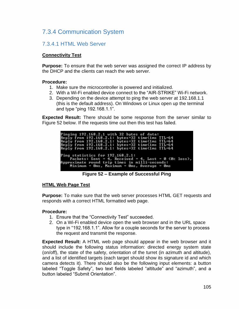
105
7.3.4 Communication System
7.3.4.1 HTML Web Server Connectivity Test Purpose: To ensure that the web server was assigned the correct IP address by the DHCP and the clients can reach the web server. Procedure:
1. Make sure the microcontroller is powered and initialized. 2. With a Wi-Fi enabled device connect to the “AIR-STRIKE” Wi-Fi network. 3. Depending on the device attempt to ping the web server at 192.168.1.1
(this is the default address). On Windows or Linux open up the terminal and type “ping 192.168.1.1”.
Expected Result: There should be some response from the server similar to Figure 52 below. If the requests time out then this test has failed.
Figure 52 – Example of Successful Ping
HTML Web Page Test Purpose: To make sure that the web server processes HTML GET requests and responds with a correct HTML formatted web page. Procedure:
1. Ensure that the “Connectivity Test” succeeded. 2. On a Wi-Fi enabled device open the web browser and in the URL space
type in “192.168.1.1”. Allow for a couple seconds for the server to process the request and transmit the response.
Expected Result: A HTML web page should appear in the web browser and it should include the following status information: directed energy system state (on/off), the state of the safety, orientation of the turret (in azimuth and altitude), and a list of identified targets (each target should show its signature id and which camera detects it). There should also be the following input elements: a button labeled “Toggle Safety”, two text fields labeled “altitude” and “azimuth”, and a button labeled “Submit Orientation”.

106
HTML GET Command Test Purpose: To make sure that the web server can process system specific commands through HTML GET requests. Procedure:
1. Ensure that the “HTML Web Page Test” succeeded. 2. On the web page press the “Toggle Safety” button. 3. In the two text fields labeled “altitude” and “azimuth” enter any degree
value from -90 to 90 that does not match the current orientation the turret. Then press the “Submit Orientation” button.
Expected Result: Refresh the page and check that the directed energy system state has been toggled and that the turret orientation has been changed to match the inputted values. Web Server Laser Safety Test Purpose: To ensure that the safety state reported on the web page is correct and that the “Toggle Safety” button correctly affects the directed energy system. Procedure:
1. On the web page check the reported state of the safety. 2. Place a valid target in front of the turret and observe the directed energy
system. 3. Press the “Toggle Safety” button and once again observe the state of the
directed energy system.
Expected Result: If the state of the safety is reported as “OFF” then the directed energy system should not fire on the valid target otherwise if the safety is reported as “ON” then the target should be fired upon.
7.3.5 External Interface Testing Test Commands via Web Server Purpose: To ensure that we can command the system externally using the HTML web server hosted by system Procedure:
1. Make sure the microcontroller is powered and initialized. 2. With a Wi-Fi enabled device connect to the “AIR-STRIKE” Wi-Fi
network
3. Navigate to the main page of the web server
4. Attempt to shut off the laser via a button on the hosted website

107
Expected Result: The webpage should update to indicate the status of the laser shutter by AIR-STRIKE checking its internal status. If the laser is connected and on it should turn off.
7.4 Integration Testing After all of our subsystem and software testing, our last testing step procedures will be comprised of system level testing. This is testing the system as a whole, after all of our parts are connected and set up for the final product. These procedures will ensure that our product works and follows the requirements that we wrote in the beginning of this document. All system level testing will be completed in a lab where class 4 lasers are allowed to be fired. All participants in the integration testing process will be required to wear the appropriate laser safe eye wear. Power Test Purpose: The first step after downloading our software onto the board is to confirm that all parts once again are getting the required power from the supply and PCB to turn on and function properly. Procedure:
1. Download a program that will communicate with each subsystem and flash the LEDs depending on if the subsystem it is communicating with
2. Utilize the push buttons to move from one subsystem to the next to ensure that LEDs do not get mixed up.
Expected Result: All subsystems will receive the correct amount of power. Correcting Errors: Since all individual testing was completed, an error must exist in the connections between subsystems. We will disconnect all of our subsystems and then reconnect them to ensure a complete connection. Red Balloon Test Purpose: To begin our testing, we will first teach the camera to locate balloon shaped objects that are red in color. We want to begin by minimizing the variables that the camera has to locate and track. Procedure:
1. Teach the Pixy to detect red balloon shaped objects. 2. Place red balloons stationary in the field of view of the cameras to
determine if the cameras can locate them. 3. Once the target is acquired, we will send the pulse to the PCB telling the
laser to fire at full strength. We want to fire at a stationary balloon so that

108
the laser remains on a constant location on the balloon. If the balloon is moving, the laser will have a harder time popping it.
Expected Result: The laser has a strong enough output to pop the balloon. Correcting Errors: If the laser does not have enough power to pop the balloon, we will have to increase the output by adjusting the variable output potentiometer. Various Colored Balloon Test Purpose: Once we are able to pop the red stationary balloon, we will then teach the camera to locate balloon shaped objects in the various colors. Procedure:
1. Inflate a balloon in the following colors: red, yellow, orange, green, blue, purple, white and black.
2. Follow the same procedure above for the Red Balloon Test. Expected Result: Our camera will detect all balloon shaped objects. Correcting Errors: If we struggle to allow for multiple colors to be detected, we will contact the Pixy manufacturer with our issues. Azimuth Tracking Test Purpose: After teaching the camera to target all of the available colors, we will then begin testing its tracking ability in the azimuth plane. Procedure:
1. First acquire the target and walk the balloon around the lab without changing its elevation level. We will be moving the balloon around the room at non-constant speeds to see how quickly the system can track an object moving at a non-constant pace. The software should track the balloon constantly and move the laser’s gimbal to point at the location of the balloon in real time.
2. After confirming a successful track, command the laser to fire.
Expected Result: The laser shall fire at the balloon to confirm that it can keep a steady track on the object when moving horizontally. Correcting Errors: If the balloon did not popped after having a successful track, we will have to increase either the power of the laser to pop the balloon quicker or increase the processing speed and signals sent to the gimbal.

109
Elevation Tracking Test Purpose: After testing the system in the azimuth plane, we will then test it in the elevation plane. Procedure:
1. We will begin by once again getting a target on a balloon. 2. Attach a much longer string to this balloon. 3. Start the balloon at ground level (or the lowest point in the field of view)
and raise the balloon varying the speeds again. 4. After a target is acquired, fire the laser.
Expected Result: The balloon will pop after being hit by the laser. Correcting Issues: If the balloon did not popped after having a successful track, we will have to increase either the power of the laser to pop the balloon quicker or increase the processing speed and signals sent to the gimbal. Azimuth and Elevation Test Purpose: Move the balloon both horizontally and vertically at the same time to force both servos to move the laser simultaneously. Procedure:
1. Plug in several fans to move the balloon in both directions horizontally and releasing and pulling the balloons string to move it vertically.
2. Confirm that the system can acquire a target. 3. After acquiring a target, fire the laser.
Expected Result: The balloon will pop after being hit by the laser. Correcting Issues: If the balloon did not popped after having a successful track, we will have to increase either the power of the laser to pop the balloon quicker or increase the processing speed and signals sent to the gimbal.

110
8.0 User Manual Due to the military application of our project, we want to ensure that all users are able to correctly operate our system without needing a large learning curve. All users will be able to use our system without needing extensive training. Note that adequate eye protection should be worn before usage, depending on the strength of the diode in use.
8.1 Power As stated in the power subheading earlier in this document, our targeting system is powered through an AC wall outlet. Applying power to the system is as easy as plugging in one power cord to a wall or surge protector. For our user interface, the operator has the option of either plugging in their device (containing an internet browser) or remaining completely mobile. The laser itself, however, is powered via a 9V battery. This is controlled by a switch on the top of the casing, which controls power to only the laser and current driver subsystem itself. To prolong the life of the battery, it is suggested that the switch be kept off in any scenario where the laser is not required.
8.2 User Interface To access our user interface, once the system is powered on, use your external device and connect to the systems Wi-Fi network by clicking on its wireless name and typing in the appropriate password. Once you are connected to the network, open any browser and type in the domain name for the website. For our demonstration, our domain name is simply www.airstrike.net. Once the page loads, the system automatically starts off in our Full Manual mode (see below for details). Here the user can begin to manipulate the device via the many options, accessible on the left.
8.2.1 Full Manual Mode The system, for safety reasons, automatically initializes in Full Manual mode so that the laser does not turn on without the user being prepared. In Full Manual mode, PixyCam tracks the target and shows where the target is located in the 3-D rendering diagram on screen. However, the servos are not commanded to track the target, nor is the laser commanded to turn on to neutralize the target. The user has full control over the system in this mode. The User is able to command the servos to point at an exact degree, in both azimuth and elevation, as well as power on the laser at any power level he/she wishes.
111
8.2.2 Manual Fire Mode Our user interface has another option called Manual Fire mode. In this mode, Pixy once again targets the target and shows the location of the target in the 3-D rendering on the screen. The servos are also commanded to track the target in preparation to neutralize the target. In this mode, the user has full control over the power output of the laser. The laser will not turn on when a target is found, nor will it not turn off when a target is neutralized. This mode is useful for tracking targets and neutralizing them when ready, rather than immediately.
8.2.3 Autonomous Mode Our final mode of operation is autonomous mode where the system works completely free without any user interaction. Once a target is found, the laser will turn on and then immediately turn off once the target is not seen any longer. This process will continue until the power is cut from the system or the user changes the mode of operation through the interface.
8.3 Programming Pixy Pixy supports tracking of up to seven different colors at a time. Programming it to these colors involves pressing the white button on the upper right corner of Pixy itself. To begin, the user must hold this button and let go when an appropriate light appears on Pixy’s LED. The first color to appear is white. Releasing at this time allows the user to adjust the white balance. Simply expose Pixy to the desired lighting conditions and press the button again to program its white balance. This should be done before programming colors to ensure Pixy is seeing the color correctly. After white, the LED will cycle through seven colors as follows: red, orange, yellow, green, cyan, blue, and violet. These are the priority of the color to be programmed, with red being highest priority and violet being lowest. Release at the desired priority to begin, then place an object of the color desired in front of Pixy. The LED on Pixy should glow a color similar to the color you are trying to program. Once the LED is the right color, click the button again to finish programming it. Be sure to keep the desired object in front of Pixy when clicking the button, or it will not work.
8.4 Troubleshooting Here are some solutions to commonly encountered issues:
1. Pixy is not tracking any targets
a. If this occurs, reset Pixy and reprogram which colors the system
shall target.
2. The target is found but the servos will not move

112
a. If this occurs, ensure that all of the pins are connected correctly to
the MCU, as well as to the servos themselves.
3. The laser will not power on
a. If this occurs, locate the current driver and see if the fault red LED
is turned on. If the LED is turned on, then first replace the battery
powering the current driver and recycle power to the system. If the
LED remains on still, this means that the driver does not detect a
load on the output, resulting in an open circuit. If this occurs, re-
connect the wires going to the laser diode.
4. The user interface has frozen or does not load
a. If this occurs, disconnect your device from the network, recycle
power to the entire system, clear the cache on your browser,
reconnect to the network and reload the page.

113
9.0 Project Standards Listed in this section are our standards for each subsystem utilized in this project.
9.1 PCB Standards Due to the diversity of printed circuit boards, each board has its own specifications and requirements. The Institute for Electrical and Electronics Engineers (IEEE) has a set of standards for designers and manufacturers to attempt to ease the process of designing a PCB and allowing it to be universal across different manufacturing platforms. During the schematic design process, in order to make designs readable for all engineers, the IEEE/ANSI 315-1975 code details the graphic symbols that shall be used. These graphic symbols are easily understood across engineering departments due to their universal resignation. For example, the symbol for a resistor or a capacitor remains the same for all engineers, regardless their companies or their disciplines. PCBs are then separated into three categories: General Electric Products, Dedicated-Service Electronic Products and High-Reliability Electronic Products. Since our project is a prototype, we followed the general electric products standards. For these standards, we followed the general-design, preferred complexity concept where producibility may not be optimized for commercial use, but rather personal use. Since our board design is not ready for commercial use, we use a lower-performance design where reliability is not a major priority since only one board will be produced. Due to this standard, we are allowed to increase the size of our PCB, ultimately increasing the trace widths and via sizes. For our design we used a minimum via size of 16 mils (where 1 mil is 1 one-thousandth of an inch) and a minimum trace width of 6 mils. For commercial products, the standard is an 8 mil via size and 3 mils for the trace width. There are also standards used for width of the layers used for the boards, the weight of the copper used for the traces, the type and amount of soldermask used and PCB dimensions. These standards are provided by the manufacturer with their tolerances they can print. These standards and specifications are provided on their website to provide the requirements the designer must follow.
9.2 Communication Standards Communicating with our many peripheral devices requires us to utilize a variety of standards for communication, depending on our desired communication speed,

114
the purpose of the communication, the number of devices, and various other factors. When communicating with the Pixy camera, we utilize the SPI standard for communication. This involves four signals, MISO (Master In Slave Out), MOSI (Master Out Slave In), SPI Clock, and Slave Select. We forgo the use of the Slave Select signal as we only use slave one device in our SPI communications. We use Big Endian 16-bit words in communication with Pixy, with a clock rate of approximately 1MHz. We operate in SPI Mode 0. In this mode the clock’s base value is 0, and data is captured on the clocks rising edge. Unfortunately, there is no real formal standard for this communication, and such conformity is difficult and limits us to one Pixy camera with our configuration. Wireless communication can occur with different devices of various make so standards are very important in order to have an established method of communication. For example the Wi-Fi network utilizes the IEEE 802.11n standard and so the system operates in the 2.4GHz band. For network security the Wi-Fi network implements WPA2 as specified in the IEEE 802.11i standard for more robust security. Another standard used is HTTP 1.1 specified in RFC 2616 which was chosen over HTTP 1.0 because of how it added caching and kept connections alive. These features translated to less processing time on the CC3200 and better performance for the external interface. The last network related standard used is the WebSocket protocol specified in RFC 6455 which establishes how the WebSocket handshake occurs and what each end of the communication needs to respond with in order to upgrade the connection. This standard was the most important to the team because the other standards had already been implemented in the CC3200, however the WebSocket standard was not and is the only network standard that had to be implemented manually.
9.3 Directed Energy Standards Any form of laser radiation can be considered dangerous. Whether the laser is only a Class I or above, any amount of laser radiation into the eye can cause serious damage. For this reason, when using the laser at high powers proper safety precautions will be taken to ensure user and spectator safety. The ANSI Z136.1 document sets the standard for safe use of a laser. Lasers are divided into classes ranging from Class I to Class IV based on their power output. While Class I lasers are generally considered safe, extended exposure to the eye can cause severe nerve damage. This document includes the proper protocol required when handling a laser. Safety goggles are the most important safety measure can take when using a laser. With the proper OD, goggles can make a powerful beam nearly harmless. When operating at full power, our laser diode emits about 650mW of optical power, making it a Class IV laser. With the beam at a focused spot size, the power is

115
sufficient to instantly blind a bystander and even cause skin damage. During testing we used Laser Safety Industries 100-10-130 goggles, which have an OD of 7+ at our operating wavelength.
116
10.0 Project Constraints In this section, we outline several of our project constraints that we ran into while
building our prototype.
10.1 One Camera vs Two Cameras In our original design we had planned to utilize two Pixy cameras in order to capitalize on the Parallax effect, which allows us to determine the range of an object much in the same manner the human brain uses the difference between the images seen by the eyes to determine depth. However, due to lack of a truly standardized SPI protocol, communication between both Pixy cameras and the CC3200 could not be reconciled. When trying to transmit data while both cameras were connected, with Slave Select correctly enabled on only one camera, the data was coming in corrupted. According to information obtained from forum communications on TI’s website, the SPI timing for the CC3200 is different than most, and while is still technically valid, is likely the cause. One way to get around this would have been to switch to I2C, or to try and implement our own SPI support for the CC3200 (although this solution would be a considerable undertaking). Due to time constraints we lowered our scope to only one camera, but switching to I2C would have been a conceivable solution for a short term fix.
10.2 CC3200 Web Server Resources In the design it states WebSockets were chosen over HTTP GET/POST for message transmission because WebSockets were faster. However the CC3200 does not support WebSockets on its default web application server so a custom server needed to be built. This meant that the web server was now being run on the main processor instead of offloaded to the network processor and cost precious system resources. To minimize the impact of the WebSocket server on the other tasks, the server limited itself to only one active connection and a time out of 1 second for connections. The end result was the other tasks such as targeting were slightly slower to finish executing, but after connection setup message transmission speed significantly increased.
10.3 Brightness of Laser Diode Disrupting Tracking One major issue we encountered when testing our system with the high-powered laser diode, is that the laser beam was too bright for PixyCam. The laser diode emits radiation at a wavelength of 405nm beam, yielding a visible purple beam. When shined onto a balloon, Pixy sees a change in color and does not detect the balloon anymore, until the laser is turned off. During several testing trials, we noticed that the laser seemed to blink on and off, rather than remaining on until the balloon popped. This occurred due to Pixy losing target of the balloon. Once the

117
laser turned on, Pixy does not detect that balloon anymore and turns off the laser, in the next frame, since the laser is turned off, Pixy locates the balloon again and turns on the laser. This process repeats indefinitely until either the balloon pops or we remove the target from the field-of-view. A solution around this problem is to use an infrared laser diode. It was suggested to use an 808nm laser diode, however, at that wavelength the camera’s detector array might pick up on this wavelength as well. We would have to go deeper into the IR with a 1064nm or 1.55µm wavelength. The down fall of these laser diodes is that they may not provide sufficient power to the balloons and/or the balloons may be transparent to these wavelengths.

118
11.0 Administrative Content
11.1 Personnel Our team is composed of four members, each with unique expertise and skills that overall contribute to the varied problems we’ve met and expect to meet as we realize the system we’ve mapped out within this paper. Every member of our team has had multiple internships and has lined up full-time employment after graduation, with intentions of pursuing graduate degrees while working.
Kevin Chau is a senior studying Computer Engineering and Secure Computing and Networks at the University of Central Florida. He has interned at Lockheed Martin, DE Technologies and Dignitas Technologies from 2010 to 2014. Kevin is currently focused in computer networking and will continue graduate studies while working at a commerical business.
Scott Greenwald is currently a senior at the University of Central Florida studying Electrical Engineering. He has interned with Lockheed Martin as a Systems Engineer throughout the summers of 2013 and 2014. After graduation, Scott will begin full time with Lockheed Martin in Orlando while continuing his education and working towards getting his Master’s Degree in Electrical Engineering.
Scott Greenwald
Kevin Chau
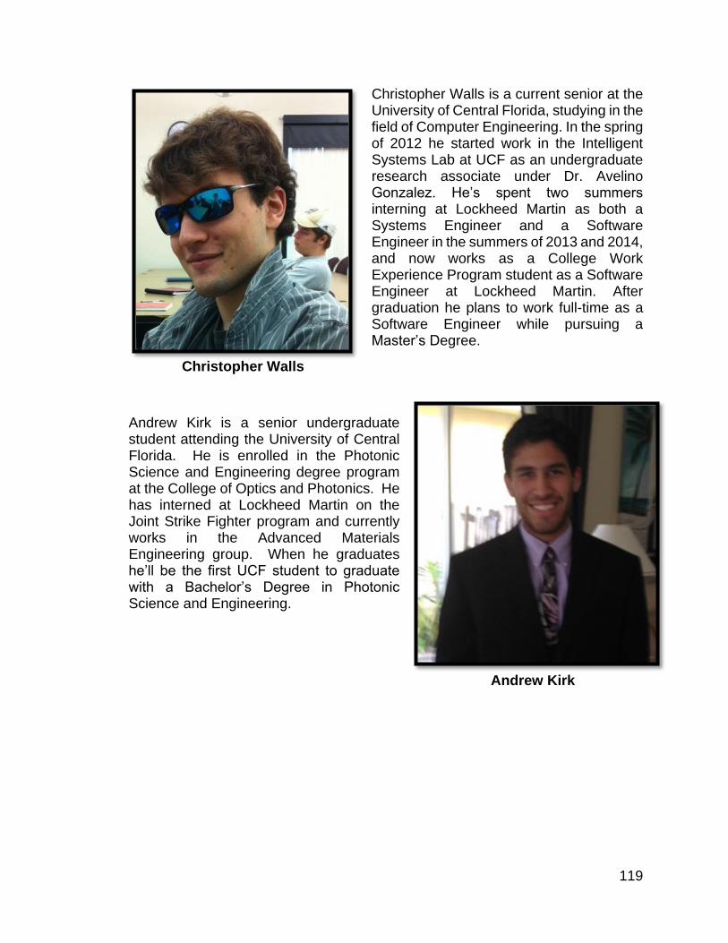
119
Christopher Walls is a current senior at the University of Central Florida, studying in the field of Computer Engineering. In the spring of 2012 he started work in the Intelligent Systems Lab at UCF as an undergraduate research associate under Dr. Avelino Gonzalez. He’s spent two summers interning at Lockheed Martin as both a Systems Engineer and a Software Engineer in the summers of 2013 and 2014, and now works as a College Work Experience Program student as a Software Engineer at Lockheed Martin. After graduation he plans to work full-time as a Software Engineer while pursuing a Master’s Degree.
Andrew Kirk is a senior undergraduate student attending the University of Central Florida. He is enrolled in the Photonic Science and Engineering degree program at the College of Optics and Photonics. He has interned at Lockheed Martin on the Joint Strike Fighter program and currently works in the Advanced Materials Engineering group. When he graduates he’ll be the first UCF student to graduate with a Bachelor’s Degree in Photonic Science and Engineering.
Christopher Walls
Andrew Kirk

120
11.2 Timeline An important aspect of managing any project is to develop a set of milestones in order to provide a set of progressing goals. This organizes the team by prioritizing separate tasks in order to ensure the most efficient usage of time. Furthermore it avoids various members arriving at a task to find that a previous task need be completed first. This can cause hold ups that negatively impact our overall efficiency and can lead to missed deadlines or times of increased stress as deadlines approach.
11.2.1 Fall 2014 The first semester devoted to this project has a focus on preparation. The primary result of these months of work should be a plan of how to proceed with the actual construction of the final product. In this time we choose our teams, determine our projects, research the manners by which we can accomplish our intended goals, and, lastly, decide upon and document our design. In this section we will detail the division of labor chosen for this semester as well as provide a timeline of by which we aimed to complete our various tasks. The timeline itself can be seen in Table 22.
Table 22 – Fall 2014 Schedule
Each member of the team had a particular overall focus when entering this project based upon personal interest as well as their educational background. We leveraged these aspects when deciding how to hand various tasks out. Each of us was thus assigned a subsystem or set of subsystems for which to write about. In doing this they were tasked to flesh out the individual requirements for their
Task Start Date End Date
Group Selection August 18th, 2014 September 2nd, 2014
Divide and Conquer Documentation
September 2nd, 2014 September 9th, 2014
Design Proposal September 9th, 2014 September 23rd, 2014
Initial Table of Contents September 23rd, 2014 October 9th, 2014
Task Designation Meeting October 9th, 2014 October 9th, 2014
Redefinition of Requirements
October 9th, 2014 October 16th, 2014
Research October 16st, 2014 October 30th, 2014
Design October 30th, 2014 November 24th, 2014
Test Plan November 24th, 2014 November 29th, 2014
Administrative & Conclusions
November 29th, 2014 December 1st, 2014
Review / Proofread December 1st, 2014 December 3rd, 2014
Printing and Binding December 3rd, 2014 December 3rd, 2014
Overall Documentation September 1st, 2014 December 4th, 2014
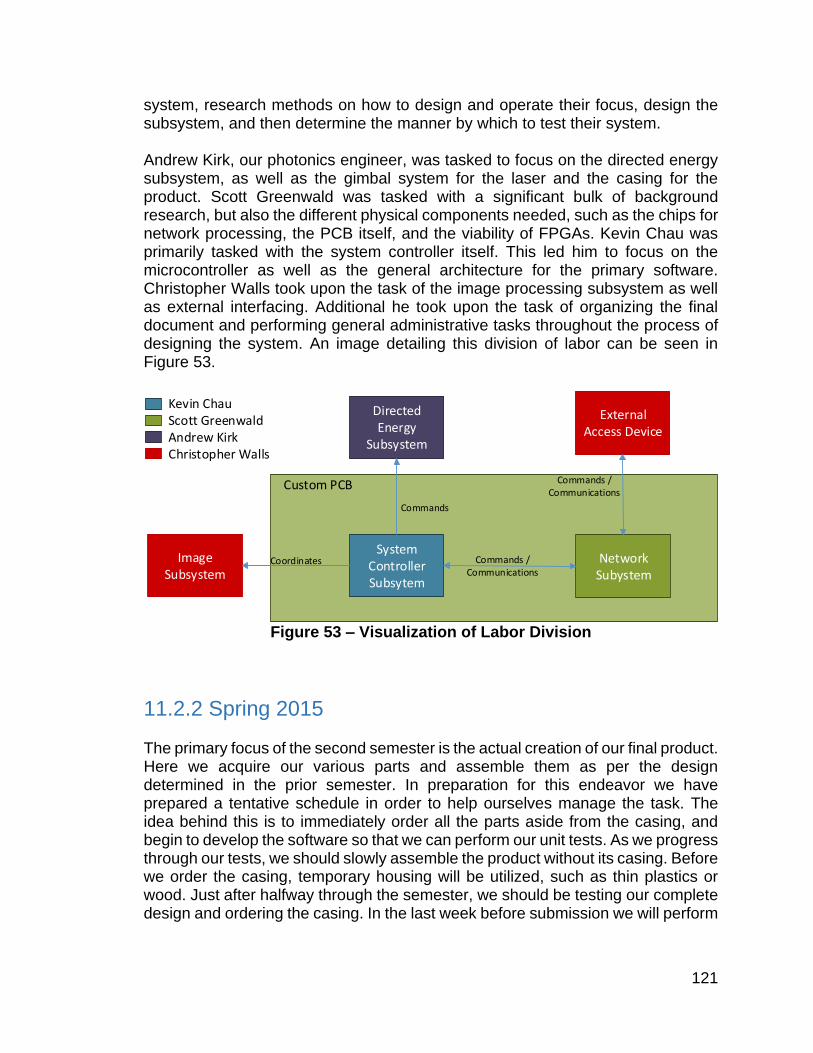
121
system, research methods on how to design and operate their focus, design the subsystem, and then determine the manner by which to test their system. Andrew Kirk, our photonics engineer, was tasked to focus on the directed energy subsystem, as well as the gimbal system for the laser and the casing for the product. Scott Greenwald was tasked with a significant bulk of background research, but also the different physical components needed, such as the chips for network processing, the PCB itself, and the viability of FPGAs. Kevin Chau was primarily tasked with the system controller itself. This led him to focus on the microcontroller as well as the general architecture for the primary software. Christopher Walls took upon the task of the image processing subsystem as well as external interfacing. Additional he took upon the task of organizing the final document and performing general administrative tasks throughout the process of designing the system. An image detailing this division of labor can be seen in Figure 53.
Image Subsystem
NetworkSubystem
System Controller Subsytem
Custom PCB
External Access Device
Directed Energy
Subsystem
Kevin ChauScott GreenwaldAndrew KirkChristopher Walls
Coordinates Commands /Communications
Commands
Commands /Communications
Figure 53 – Visualization of Labor Division
11.2.2 Spring 2015 The primary focus of the second semester is the actual creation of our final product. Here we acquire our various parts and assemble them as per the design determined in the prior semester. In preparation for this endeavor we have prepared a tentative schedule in order to help ourselves manage the task. The idea behind this is to immediately order all the parts aside from the casing, and begin to develop the software so that we can perform our unit tests. As we progress through our tests, we should slowly assemble the product without its casing. Before we order the casing, temporary housing will be utilized, such as thin plastics or wood. Just after halfway through the semester, we should be testing our complete design and ordering the casing. In the last week before submission we will perform

122
final testing to ensure it all works within the casing. Table 23 below represents this timeline.
Table 23 – Spring 2015 Schedule
11.3 Budget After our decisions were made, our total cost turned out to be $868.08. This varied quite far from our initial prospects due to several design decisions. The primary alteration was the decision to not use an FPGA to assist in image processing. Secondarily, through the TI Lab at the University of Central Florida, we were permitted to borrow the developing kits for each of our chosen TI chips. This lowers our development costs significantly, as we do not have to purchase any development boards when we finally design our final product. The budget calculation can be seen in Table 24 and a distribution of this can be seen in Figure 54.
Task Start Date End Date
Order Parts (Except Casing) December 10th, 2014 January 19th, 2015
Initial Group Meeting January 9th, 2015 January 9th, 2015
Code Initial Software for Microcontroller
January 19th, 2015 January 28th, 2015
Test Pixy Cameras January 19th, 2015 January 23rd, 2015
Test Servos January 19th, 2015 January 28th, 2015
Test Basic Communications to AIR-STRIKE
January 28th, 2015 February 9th, 2015
Develop Interface between Pixy Cameras and AIR-STRIKE
February 9th, 2015 February 23rd, 2015
Develop Initial External Interface Windows GUI
February 9th, 2015 February 23rd, 2015
Assemble Laser February 9th, 2015 March 9th, 2015
Assemble Gimbal System February 9th, 2015 March 9th, 2015
Assembly without Casing (for Testing)
March 9th, 2015 March 23rd, 2015
Order Casing March 23rd, 2015 March 30th, 2015
Testing March 23rd, 2015 April 13th, 2015
Assemble into Casing April 13th, 2015 April 20th, 2015
Final Testing April 20th, 2015 April 25th, 2015
Submission April 25th, 2015 April 30th, 2015

123
Table 24 – Budget
Figure 54 – Budget Distribution
11.4 Sponsorship Foremost, we would like to extend our gratitude and thanks to Boeing for their generous sponsorship of our product. Without their support, this project would be far more difficult to realize with our limited personal budgets. Our project is most applicable to the defense industry based upon its purpose as a miniaturization of an automated anti-air system. For this reason we sought sponsorship from Boeing whom works with the U.S. military to design many wartime products. From them we received an allotment of $900.00 in order to pursue our project, which was based upon our initial cost estimates.

124
12.0 Conclusion Throughout the semester the team made many discoveries about the process of crafting a professional design. Primarily this involved the difference in quality of work expected as well as the sheer volume of aspects to document in relation to our design. Furthermore we came to understand just how important it was to fully research components before we purchased them. If we had attempted to follow through with our initial ideas, we’d likely find ourselves deep into the following semester with only a fancy paperweight to our name. In this section we delve into some of the lessons learned and decisions made throughout the design process. The importance of organization became quickly apparent to us as the semester pushed on. Initially we only loosely assigned tasks and were unspecific about formatting, word processor usage, and which decisions had already been made. An importance consequence to this was the rush in the last week by two members to quickly compound as much information into text as they could. This led to some sections filling unrefined and less substantial than others despite having the necessary details. However, certain aspects were made significantly easier when organization was implement. An instance of this is the table of contents, which is automatically created based upon the text designated as headers. Furthermore, the usage of font ‘styles’ in Microsoft Word made it especially easy to merge different documents as Word would automatically convert text to the proper style based upon its style in the group members original documents. In terms of the project itself, many features were taken out or replaced as we started to understand the implications of certain choices in our design. For instance, we discarded the idea of an FPGA on the principle that they are quite difficult to integrate into a PCB design and connect to other components. As none of us had proper experience with an FPGA in any capacity and their relative costliness, we decided to abandon their usage. Similarly we decided to remove our plans for a Raspberry Pi in our system due to their relative slowness when performing image processing techniques. In the end it was best to find hardware specialized in the process, leading us to Pixy. These are merely a few examples of the lessons that came from our work this semester. Although the most important lesson parted was the understanding of how to create a truly professional document. This experience will be vital as we pursue our careers where documents such as this are commonplace. We can then look back upon this semester as an experience that ensured we would not produce documentation that was illegible, disorganized, and insufficient. While this may not be the best design document, it taught us a lot about what makes up the best design document. And so we end this document with a readiness to pursue the realization of our design in the hopes that it will be more successful than we could have originally hoped.

125
Appendices
Appendix A – Permissions
Permission from Charmed Labs to use their Images
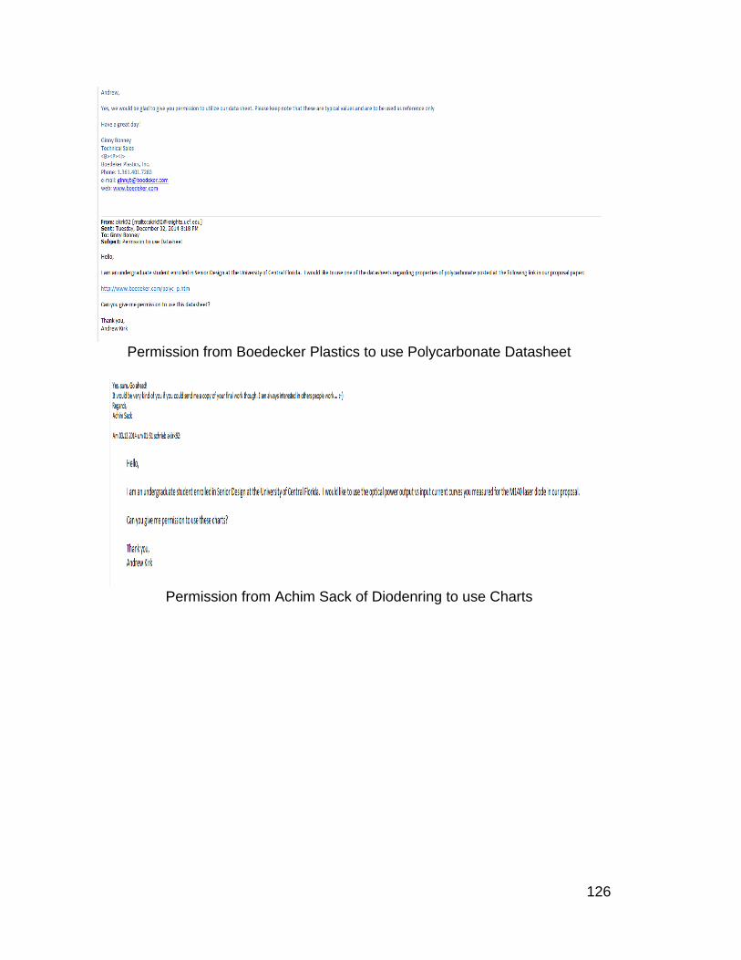
126
Permission from Boedecker Plastics to use Polycarbonate Datasheet
Permission from Achim Sack of Diodenring to use Charts

127
Request for Permission to use PCB Manufacturing Image
Request to Carolina Community College regarding Schematic of Laser Beam
Divergence

128
Request to Erchonia regarding chart on laser
classes.
Request to Innolasers regarding FlexMod P3
datasheet
Request to LaserVision regarding safety eyewear
lens datashet
Request to LightPath Technologies regarding
collimating lens datasheet

129
Request to Olympus regarding chart depicting
laser beam modes
Request to Solid Concepts regarding Nylon12 datasheet

130
Appendix B – References
[1] K. Sheehan, "The laser's potential for weaponry: SPIE Professional," April 2010. [Online]. Available: http://spie.org/x39813.xml. [Accessed 29 November 2014].
[2] H. Srebrnik, "The rise of drone warfare," Journal Pioneer, 23 November 2014. [Online]. Available: http://www.journalpioneer.com/Opinion/Columnists/2014-11-23/article-3949539/The-rise-of-drone-warfare/1. [Accessed 30 11 2014].
[3] O. Svelto, Principles of Lasers FIfth Edition, Springer, 2010.
[4] S. T. Maker, "Sparkfun," [Online]. Available: https://learn.sparkfun.com/tutorials/pcb-basics.
[5] M. Grant, "Quick Start for Beginners to Drive a Stepper Motor," Freescale Semiconductors, June 2005.
[6] A. Circuits, "4pcb," 29 09 2008. [Online]. Available: http://www.4pcb.com/media/PCBArtistTutorial.pdf.
[7] "Trendnet," [Online]. Available: http://www.trendnet.com/products/proddetail.asp?prod=180_TEW-664UB.
[8] Texas Instruments, "TM4C129DNCPDT Tiva C Series Microcontroller," June 2014. [Online]. Available: http://www.ti.com/lit/gpn/tm4c129dncpdt. [Accessed 14 11 2014].
[9] Texas Instruments, "TivaWare™ for C Series (Complete)," February 2014. [Online]. Available: http://www.ti.com/lit/pdf/spmu297. [Accessed 14 11 2014].
[10] "Texas Instruments," 06 2014. [Online]. Available: http://www.ti.com/product/CC3100/datasheet.
[11] "Sunstone Circuits," [Online]. Available: www.sunstone.com.
[12] "ST life.augmented," June 2014. [Online]. Available: http://www.st.com/st-web-ui/static/active/en/resource/technical/document/datasheet/DM00050585.pdf.
[13] "SparkFun," [Online]. Available: https://www.sparkfun.com/products/12574.
[14] Baldor Electric Company, Servo Control Facts, 2001.
[15] Engadget, "Rasperry Pi A/B Specs," [Online]. Available: http://www.engadget.com/products/raspberry-pi/a-b/specs/. [Accessed 07 11 2014].
[16] "Pad2Pad," [Online]. Available: www.pad2pad.com.
[17] "PA International," [Online]. Available: http://www.pa-international.com/products/pcb-and-pcba.
[18] "Netgear," 2014. [Online]. Available: http://www.netgear.com/home/products/networking/wifi-adapters/WNDA3100.aspx.
131
[19] Texas Instruments, "MSP430F15x, MSP430F16x, MSP430F161x MIXED SIGNAL MICROCONTROLLER," October 2002. [Online]. Available: http://www.ti.com/lit/ds/symlink/msp430f1611.pdf. [Accessed 14 11 2014].
[20] "LSR," 2013. [Online]. Available: http://www.lsr.com/downloads/products/330-0132.pdf.
[21] "Linksys," [Online]. Available: http://www.linksys.com/en-apac/products/adapters/AE1000.
[22] "Landronix," 2014. [Online]. Available: http://www.lantronix.com/device-networking/embedded-device-servers/xpico-wifi.html.
[23] "gi," 2014. [Online]. Available: http://www.digi.com/products/wireless-wired-embedded-solutions/zigbee-rf-modules/point-multipoint-rfmodules/xbee-pro-868.
[24] Nautilus Integration, "FlexMod P3 UserManual," 2010. [Online]. Available: https://innolasers.com/shop/index.php?id_product=11&controller=product.
[25] "Digi," 2014. [Online]. Available: http://www.digi.com/products/wireless-wired-embedded-solutions/zigbee-rf-modules/zigbee-mesh-module/xbee-digimesh-2-4#overview.
[26] "Digi," 2014. [Online]. Available: http://www.digi.com/products/wireless-wired-embedded-solutions/zigbee-rf-modules/point-multipoint-rfmodules/xbee-series1-module#overview.
[27] "Digi," 2013. [Online]. Available: http://www.digi.com/products/wireless-wired-embedded-solutions/zigbee-rf-modules/point-multipoint-rfmodules/xbee-wi-fi#docs.
[28] Texas Instruments, "CC3200 SimpleLink™ Wi-Fi® and Internet-of-Things solution, a Single-Chip Wireless MCU," June 2014. [Online]. Available: http://www.ti.com/lit/gpn/cc3200. [Accessed 14 11 2014].
[29] Texas Instruments, "CC2560 Bluetooth Controller," January 2014. [Online]. Available: http://www.ti.com/lit/gpn/cc2560. [Accessed 14 11 2014].
[30] LightPath Technologies, "Blue Collimating Lens Datasheet," 2012. [Online]. Available: http://lightpathtechnologies.com.
[31] "Battery University," [Online]. Available: http://batteryuniversity.com/learn/article/whats_the_best_battery.
[32] "Advanced Circuits," [Online]. Available: www.4pcb.com.


