7. Electrical Characteristics............................................. 28 7.1 DC Characteristics ................................................... 28 7.2 AC Timing Characteristics ...................................... 28
7.2.1 Cold Reset ........................................................ 28 7.2.2 Warm Reset...................................................... 29 7.2.3 AC-Link Clocks ............................................... 29 7.2.4 Data Output and Input Times ........................... 30 7.2.5 Signal Rise and Fall Times .............................. 31 7.2.6 AC-Link Low Power Mode Timing................. 32 7.2.7 ATE Test Mode................................................ 32 7.2.8 AC-Link IO Pin Capacitance and Loading ...... 33 7.2.9 SPDIF Output................................................... 33 7.2.10 BIT-CLK and SDATA-IN State .................... 33
8. Analog Performance Characteristics .......................... 34 9. Design Suggestions........................................................ 35
1. Features High performance CODEC with high S/N ratio (>90 dB) 18-bit ADC and 20-bit DAC resolution Compliant with AC’97 2.2 specifications 18-bit stereo full-duplex CODEC with independent and variable sampling rate 4 analog line-level stereo inputs with 5-bit volume control: LINE_IN,CD,VIDEO,AUX 2 analog line-level mono inputs: PC_BEEP,PHONE_IN Mono output with 5-bit volume control Stereo output with 5-bit volume control 6 channel slot selectable DAC output for multi-channel applications One standard MIC input, and one dedicated Front-MIC input for front panel applications (software selectable) LINE Inputs shared with surround output; MIC1 and MIC2 shared with Center and LFE output 2 MIC inputs, which are software selectable Power management capabilities 3D Stereo enhancement Embedded 50mW/20ohm OP at front LINE output External amplifier power down capability Digital S/PDIF output Digital S/PDIF input. (ALC650 Rev. E or later) No external crystal/clock required Supports 1 general purpose I/O pin Power supply: Digital:3.3V; Analog: 5V/3.3V Standard 48-Pin LQFP Package
2. General Description The ALC650 is an 18-bit, full duplex AC'97 2.2 compatible stereo audio CODEC designed for PC multimedia systems, including host/soft audio and AMR/CNR based designs. The ALC650 incorporates proprietary converter technology to achieve a high SNR, greater than 90 dB. The ALC650 AC'97 CODEC supports multiple CODEC extensions with independent variable sampling rates and built-in 3D effects. The ALC650 CODEC provides three pairs of stereo outputs with independent volume controls, a mono output, and multiple stereo and mono inputs, along with flexible mixing, gain and mute functions to provide a complete integrated audio solution for PCs. The digital interface circuitry of the ALC650 CODEC operates from a 3.3V power supply with EAPD (External Amplifier Power Down) control for use in notebook and PC applications. The ALC650 integrates a 50mW/20ohm headset audio amplifier into the CODEC, which can save BOM costs. The ALC650 also supports an AC’97 2.2 compliant SPDIF out function which allows easy connection from the PC to consumer electronic products, such as AC3 decoder/speaker and mini disk. The ALC650 CODEC supports host/soft audio from Intel 810/815/820/845 chipsets as well as audio controller based VIA/SIS/ALI chipsets. Bundled Windows series drivers (Win95/98/ME/2000/XP/NT) and sound effect utilities (supporting Karaoke, emulation of 26 sound environments, and 10-band equalizer) provide a more comprehensive entertainment package for PC users. Finally, internal PLL circuits generate required timing signals, eliminating the need for external clocking devices.
Name Type Pin No Description Characteristic Definition RESET# I 11 AC'97 master H/W reset Schmitt input,VL=0.3Vdd, VH=0.4Vdd XTL-IN I 2 Crystal input pad (24.576Mhz) Crystal input pad
XTL-OUT O 3 Crystal output pad Crystal output pad SYNC I 10 Sample Sync (48Khz) Schmitt input,VL=0.3Vdd, VH=0.4Vdd
BIT-CLK IO 6 Bit clock output (12.288Mhz) CMOS input/output, Vt=0.35Vdd, internal pulled low by a 100K resistor.
SDATA-OUT
I 5 Serial TDM AC’97 output Schmitt input,VL=0.3Vdd, VH=0.4Vdd
SDATA-IN O 8 Serial TDM AC’97 input CMOS output, internal pulled low by a 100K resistor.
GPIO0 I/O 45 General Purpose I/O 0 XTLSEL I 46 Crystal Selection S/PDIFI /
EAPD I/O 47 S/PDIF input / External
Amplifier power down control Digital input / output
S/PDIFO O 48 S/PDIF output Digital output TOTAL: 11 Pins
5.2 Analog I/O Pins Name Type Pin No Description Characteristic Definition
PC-BEEP I 12 PC speaker input Analog input (1Vrms) PHONE I 13 Speaker phone input Analog input (1Vrms) AUX-L I 14 AUX Left channel Analog input (1Vrms) AUX-R I 15 AUX Right channel Analog input (1Vrms)
VIDEO-L I 16 Video audio Left channel Analog input (1Vrms) VIDEO-R I 17 Video audio Right channel Analog input (1Vrms)
CD-L I 18 CD audio Left channel Analog input (1Vrms) CD-GND I 19 CD audio analog GND Analog input (1Vrms)
CD-R I 20 CD audio Right channel Analog input (1Vrms) MIC1 I / O 21 First Mic input / CEN-OUT Analog input (1Vrms) / Analog output (1Vrms) MIC2 O 22 Alternative LFE-OUT Analog output (1Vrms)
LINE-L I / O 23 Line-In Left channel / S-OUT-L Analog input (1Vrms) / Analog output (1Vrms) LINE-R I / O 24 Line-In Right channel / S-OUT-
R Analog input (1Vrms) / Analog output (1Vrms)
Front-MIC I 34 Dedicated MIC Input Analog input (1Vrms) for front panel MIC input LINE-OUT-L O 35 Line-Out Left channel Analog output (1Vrms) LINE-OUT-R O 36 Line-Out Right channel Analog output (1Vrms) MONO-OUT O 37 Speaker Phone output Analog output (1Vrms) S-OUT-L O 39 Surround Out Left channel Analog output (1Vrms) S-OUT-R O 41 Surround Out Right channel Analog output (1Vrms) CEN-OUT O 43 Center Out channel Analog output (1Vrms) LFE-OUT O 44 Low Frequency Effect Out
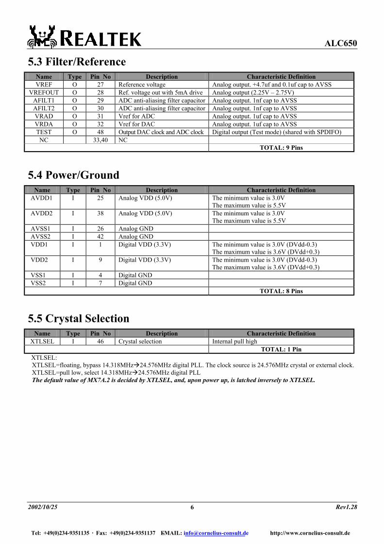
5.3 Filter/Reference Name Type Pin No Description Characteristic Definition VREF O 27 Reference voltage Analog output. +4.7uf and 0.1uf cap to AVSS
VREFOUT O 28 Ref. voltage out with 5mA drive Analog output (2.25V – 2.75V) AFILT1 O 29 ADC anti-aliasing filter capacitor Analog output. 1nf cap to AVSS AFILT2 O 30 ADC anti-aliasing filter capacitor Analog output. 1nf cap to AVSS VRAD O 31 Vref for ADC Analog output. 1uf cap to AVSS VRDA O 32 Vref for DAC Analog output. 1uf cap to AVSS TEST O 48 Output DAC clock and ADC clock Digital output (Test mode) (shared with SPDIFO) NC 33,40 NC
TOTAL: 9 Pins
5.4 Power/Ground Name Type Pin No Description Characteristic Definition
AVDD1 I 25 Analog VDD (5.0V) The minimum value is 3.0V The maximum value is 5.5V
AVDD2 I 38 Analog VDD (5.0V) The minimum value is 3.0V The maximum value is 5.5V
AVSS1 I 26 Analog GND AVSS2 I 42 Analog GND VDD1 I 1 Digital VDD (3.3V) The minimum value is 3.0V (DVdd-0.3)
The maximum value is 3.6V (DVdd+0.3) VDD2 I 9 Digital VDD (3.3V) The minimum value is 3.0V (DVdd-0.3)
The maximum value is 3.6V (DVdd+0.3) VSS1 I 4 Digital GND VSS2 I 7 Digital GND
TOTAL: 8 Pins
5.5 Crystal Selection Name Type Pin No Description Characteristic Definition
XTLSEL I 46 Crystal selection Internal pull high TOTAL: 1 Pin XTLSEL:
XTLSEL=floating, bypass 14.318MHz 24.576MHz digital PLL. The clock source is 24.576MHz crystal or external clock. XTLSEL=pull low, select 14.318MHz 24.576MHz digital PLL The default value of MX7A.2 is decided by XTLSEL, and, upon power up, is latched inversely to XTLSEL.
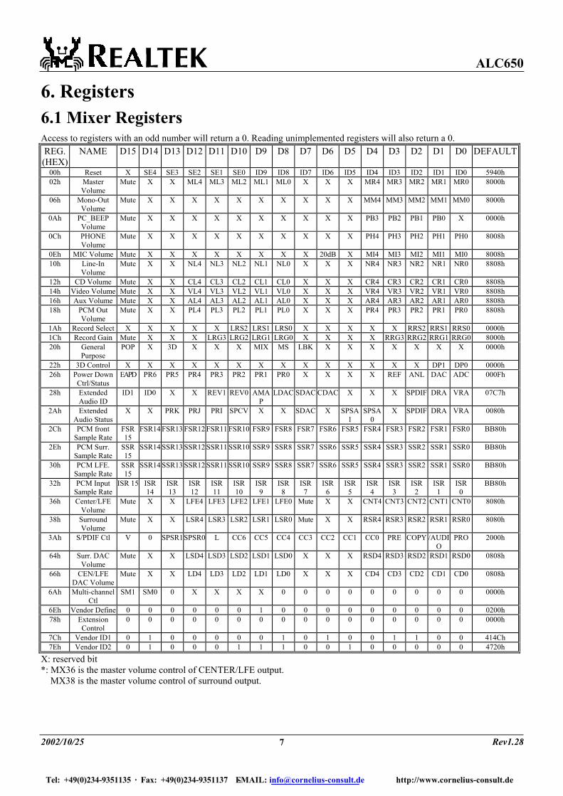
6. Registers 6.1 Mixer Registers Access to registers with an odd number will return a 0. Reading unimplemented registers will also return a 0. REG. (HEX)
Volume Mute X X ML4 ML3 ML2 ML1 ML0 X X X MR4 MR3 MR2 MR1 MR0 8000h
06h Mono-Out Volume
Mute X X X X X X X X X X MM4 MM3 MM2 MM1 MM0 8000h
0Ah PC_BEEP Volume
Mute X X X X X X X X X X PB3 PB2 PB1 PB0 X 0000h
0Ch PHONE Volume
Mute X X X X X X X X X X PH4 PH3 PH2 PH1 PH0 8008h
0Eh MIC Volume Mute X X X X X X X X 20dB X MI4 MI3 MI2 MI1 MI0 8008h 10h Line-In
Volume Mute X X NL4 NL3 NL2 NL1 NL0 X X X NR4 NR3 NR2 NR1 NR0 8808h
12h CD Volume Mute X X CL4 CL3 CL2 CL1 CL0 X X X CR4 CR3 CR2 CR1 CR0 8808h 14h Video Volume Mute X X VL4 VL3 VL2 VL1 VL0 X X X VR4 VR3 VR2 VR1 VR0 8808h 16h Aux Volume Mute X X AL4 AL3 AL2 AL1 AL0 X X X AR4 AR3 AR2 AR1 AR0 8808h 18h PCM Out
Volume Mute X X PL4 PL3 PL2 PL1 PL0 X X X PR4 PR3 PR2 PR1 PR0 8808h
1Ah Record Select X X X X X LRS2 LRS1 LRS0 X X X X X RRS2 RRS1 RRS0 0000h 1Ch Record Gain Mute X X X LRG3 LRG2 LRG1 LRG0 X X X X RRG3 RRG2 RRG1 RRG0 8000h 20h General
Purpose POP X 3D X X X MIX MS LBK X X X X X X X 0000h
22h 3D Control X X X X X X X X X X X X X X DP1 DP0 0000h 26h Power Down
Ctrl/Status EAPD PR6 PR5 PR4 PR3 PR2 PR1 PR0 X X X X REF ANL DAC ADC 000Fh
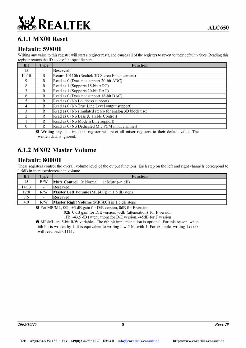
6.1.1 MX00 Reset Default: 5980H Writing any value to this register will start a register reset, and causes all of the registers to revert to their default values. Reading this register returns the ID code of the specific part.
Bit Type Function 15 - Reserved
14:10 R Return 10110h (Realtek 3D Stereo Enhancement) 9 R Read as 0 (Does not support 20-bit ADC) 8 R Read as 1 (Supports 18-bit ADC) 7 R Read as 1 (Supports 20-bit DAC) 6 R Read as 0 (Does not support 18-bit DAC) 5 R Read as 0 (No Loudness support) 4 R Read as 0 (No True Line Level output support) 3 R Read as 0 (No simulated stereo for analog 3D block use) 2 R Read as 0 (No Bass & Treble Control) 1 R Read as 0 (No Modem Line support) 0 R Read as 0 (No Dedicated Mic PCM input channel)
Writing any data into this register will reset all mixer registers to their default value. The written data is ignored.
6.1.2 MX02 Master Volume Default: 8000H These registers control the overall volume level of the output functions. Each step on the left and right channels correspond to 1.5dB in increase/decrease in volume.
Bit Type Function 15 R/W Mute Control 0: Normal 1: Mute (-∞ dB)
14:13 - Reserved 12:8 R/W Master Left Volume (ML[4:0]) in 1.5 dB steps 7:5 - Reserved 4:0 R/W Master Right Volume (MR[4:0]) in 1.5 dB steps
For MR/ML, 00h +3 dB gain for D/E version, 0dB for F version 02h 0 dB gain for D/E version, -3dB (attenuation) for F version 1Fh -43.5 dB (attenuation) for D/E version, -45dB for F version
MR/ML are 5-bit R/W variables. The 6th bit implementation is optional. For this reason, when 6th bit is written by 1, it is equivalent to writing low 5-bit with 1. For example, writing 1xxxxx will read back 01111.
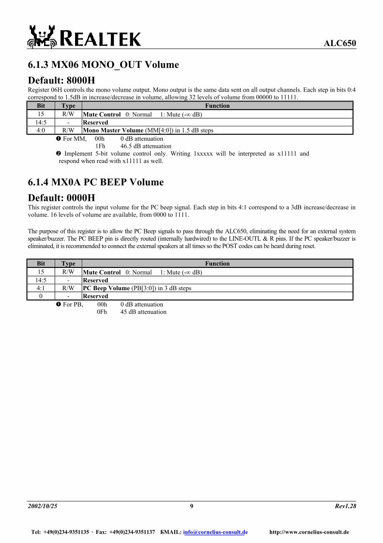
6.1.3 MX06 MONO_OUT Volume Default: 8000H Register 06H controls the mono volume output. Mono output is the same data sent on all output channels. Each step in bits 0:4 correspond to 1.5dB in increase/decrease in volume, allowing 32 levels of volume from 00000 to 11111.
Bit Type Function 15 R/W Mute Control 0: Normal 1: Mute (-∞ dB)
14:5 - Reserved 4:0 R/W Mono Master Volume (MM[4:0]) in 1.5 dB steps
For MM, 00h 0 dB attenuation 1Fh 46.5 dB attenuation
Implement 5-bit volume control only. Writing 1xxxxx will be interpreted as x11111 and respond when read with x11111 as well.
6.1.4 MX0A PC BEEP Volume Default: 0000H This register controls the input volume for the PC beep signal. Each step in bits 4:1 correspond to a 3dB increase/decrease in volume. 16 levels of volume are available, from 0000 to 1111.
The purpose of this register is to allow the PC Beep signals to pass through the ALC650, eliminating the need for an external system speaker/buzzer. The PC BEEP pin is directly routed (internally hardwired) to the LINE-OUTL & R pins. If the PC speaker/buzzer is eliminated, it is recommended to connect the external speakers at all times so the POST codes can be heard during reset.
Bit Type Function 15 R/W Mute Control 0: Normal 1: Mute (-∞ dB)
14:5 - Reserved 4:1 R/W PC Beep Volume (PB[3:0]) in 3 dB steps 0 - Reserved
For PB, 00h 0 dB attenuation 0Fh 45 dB attenuation
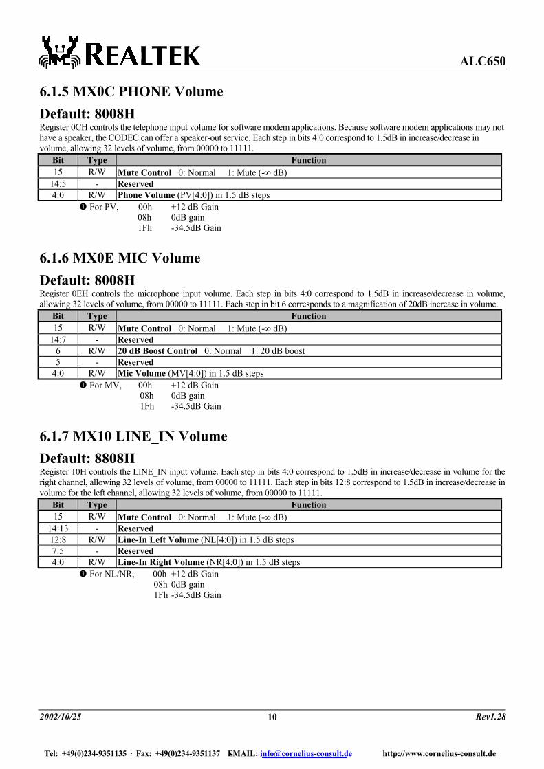
6.1.5 MX0C PHONE Volume Default: 8008H Register 0CH controls the telephone input volume for software modem applications. Because software modem applications may not have a speaker, the CODEC can offer a speaker-out service. Each step in bits 4:0 correspond to 1.5dB in increase/decrease in volume, allowing 32 levels of volume, from 00000 to 11111.
Bit Type Function 15 R/W Mute Control 0: Normal 1: Mute (-∞ dB)
14:5 - Reserved 4:0 R/W Phone Volume (PV[4:0]) in 1.5 dB steps
For PV, 00h +12 dB Gain 08h 0dB gain 1Fh -34.5dB Gain
6.1.6 MX0E MIC Volume Default: 8008H Register 0EH controls the microphone input volume. Each step in bits 4:0 correspond to 1.5dB in increase/decrease in volume, allowing 32 levels of volume, from 00000 to 11111. Each step in bit 6 corresponds to a magnification of 20dB increase in volume.
Bit Type Function 15 R/W Mute Control 0: Normal 1: Mute (-∞ dB)
14:7 - Reserved 6 R/W 20 dB Boost Control 0: Normal 1: 20 dB boost 5 - Reserved
4:0 R/W Mic Volume (MV[4:0]) in 1.5 dB steps For MV, 00h +12 dB Gain
08h 0dB gain 1Fh -34.5dB Gain
6.1.7 MX10 LINE_IN Volume Default: 8808H Register 10H controls the LINE_IN input volume. Each step in bits 4:0 correspond to 1.5dB in increase/decrease in volume for the right channel, allowing 32 levels of volume, from 00000 to 11111. Each step in bits 12:8 correspond to 1.5dB in increase/decrease in volume for the left channel, allowing 32 levels of volume, from 00000 to 11111.
Bit Type Function 15 R/W Mute Control 0: Normal 1: Mute (-∞ dB)
14:13 - Reserved 12:8 R/W Line-In Left Volume (NL[4:0]) in 1.5 dB steps 7:5 - Reserved 4:0 R/W Line-In Right Volume (NR[4:0]) in 1.5 dB steps
For NL/NR, 00h +12 dB Gain 08h 0dB gain 1Fh -34.5dB Gain
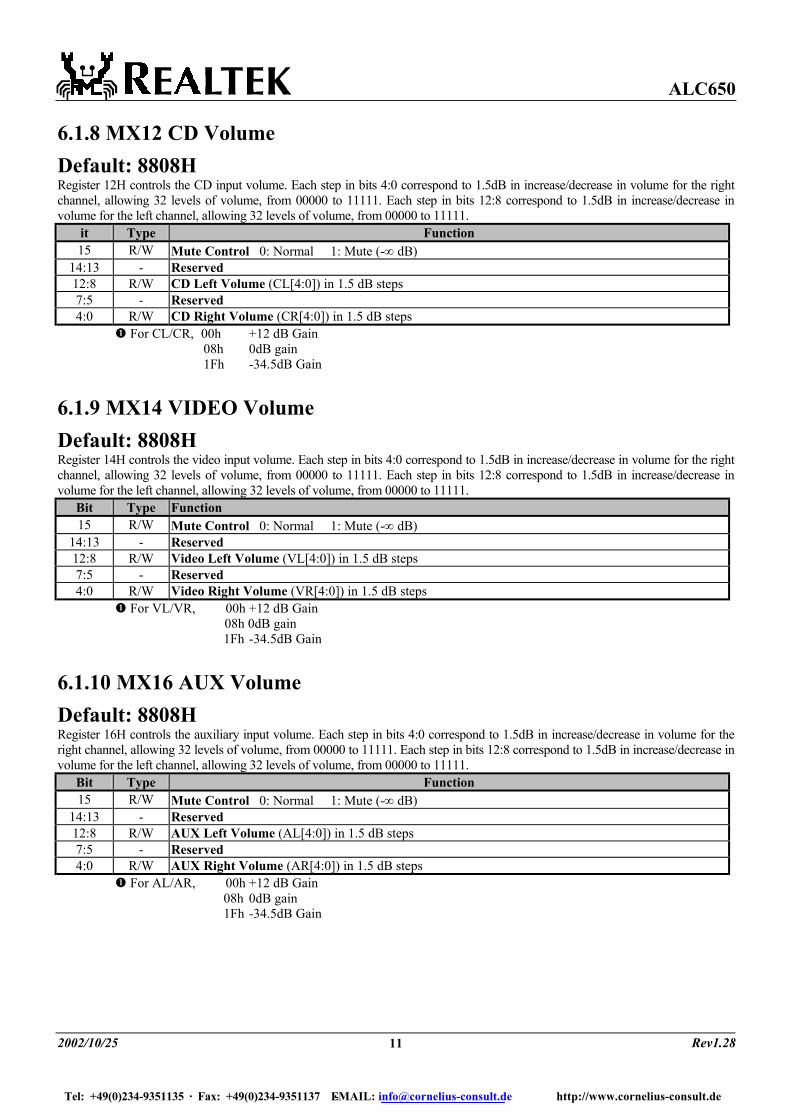
6.1.8 MX12 CD Volume Default: 8808H Register 12H controls the CD input volume. Each step in bits 4:0 correspond to 1.5dB in increase/decrease in volume for the right channel, allowing 32 levels of volume, from 00000 to 11111. Each step in bits 12:8 correspond to 1.5dB in increase/decrease in volume for the left channel, allowing 32 levels of volume, from 00000 to 11111.
it Type Function 15 R/W Mute Control 0: Normal 1: Mute (-∞ dB)
14:13 - Reserved 12:8 R/W CD Left Volume (CL[4:0]) in 1.5 dB steps 7:5 - Reserved 4:0 R/W CD Right Volume (CR[4:0]) in 1.5 dB steps
For CL/CR, 00h +12 dB Gain 08h 0dB gain 1Fh -34.5dB Gain
6.1.9 MX14 VIDEO Volume Default: 8808H Register 14H controls the video input volume. Each step in bits 4:0 correspond to 1.5dB in increase/decrease in volume for the right channel, allowing 32 levels of volume, from 00000 to 11111. Each step in bits 12:8 correspond to 1.5dB in increase/decrease in volume for the left channel, allowing 32 levels of volume, from 00000 to 11111.
Bit Type Function 15 R/W Mute Control 0: Normal 1: Mute (-∞ dB)
14:13 - Reserved 12:8 R/W Video Left Volume (VL[4:0]) in 1.5 dB steps 7:5 - Reserved 4:0 R/W Video Right Volume (VR[4:0]) in 1.5 dB steps
For VL/VR, 00h +12 dB Gain 08h 0dB gain 1Fh -34.5dB Gain
6.1.10 MX16 AUX Volume Default: 8808H Register 16H controls the auxiliary input volume. Each step in bits 4:0 correspond to 1.5dB in increase/decrease in volume for the right channel, allowing 32 levels of volume, from 00000 to 11111. Each step in bits 12:8 correspond to 1.5dB in increase/decrease in volume for the left channel, allowing 32 levels of volume, from 00000 to 11111.
Bit Type Function 15 R/W Mute Control 0: Normal 1: Mute (-∞ dB)
14:13 - Reserved 12:8 R/W AUX Left Volume (AL[4:0]) in 1.5 dB steps 7:5 - Reserved 4:0 R/W AUX Right Volume (AR[4:0]) in 1.5 dB steps
For AL/AR, 00h +12 dB Gain 08h 0dB gain 1Fh -34.5dB Gain
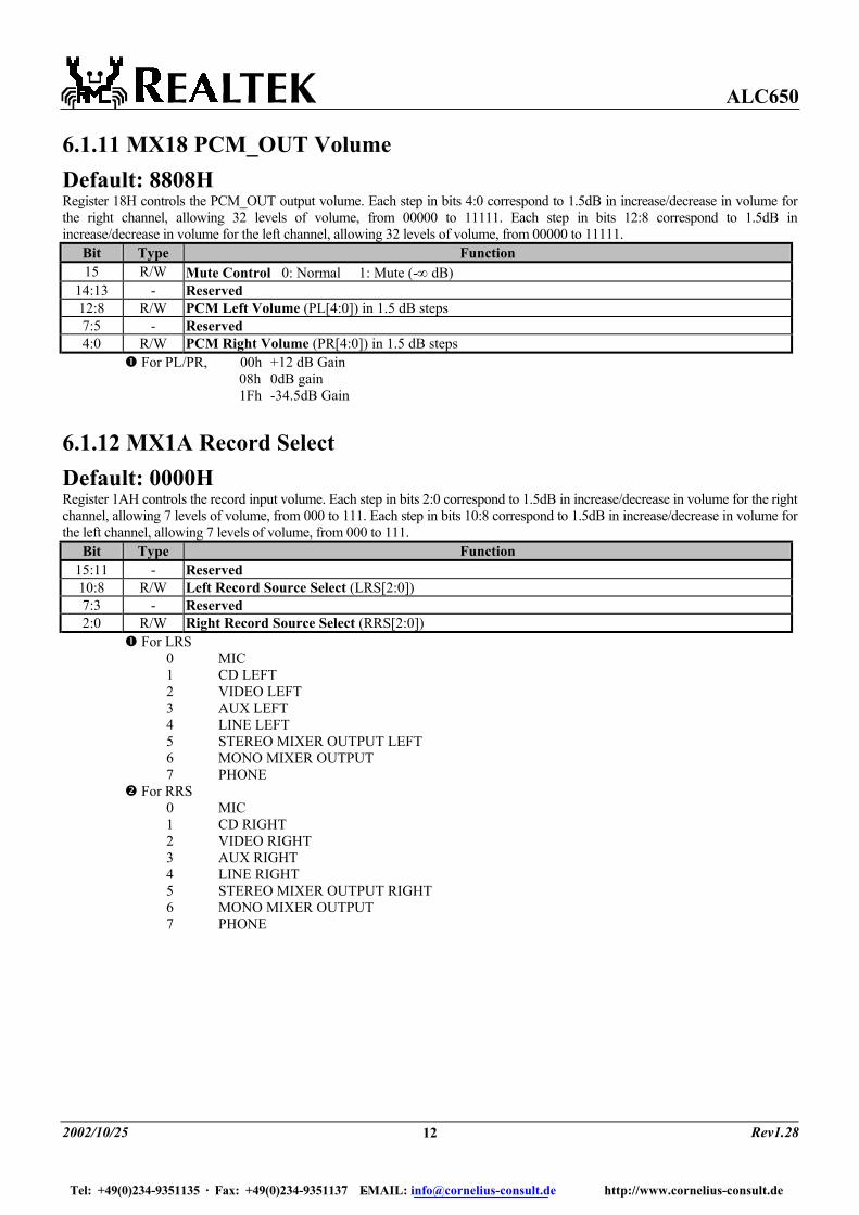
6.1.11 MX18 PCM_OUT Volume Default: 8808H Register 18H controls the PCM_OUT output volume. Each step in bits 4:0 correspond to 1.5dB in increase/decrease in volume for the right channel, allowing 32 levels of volume, from 00000 to 11111. Each step in bits 12:8 correspond to 1.5dB in increase/decrease in volume for the left channel, allowing 32 levels of volume, from 00000 to 11111.
Bit Type Function 15 R/W Mute Control 0: Normal 1: Mute (-∞ dB)
14:13 - Reserved 12:8 R/W PCM Left Volume (PL[4:0]) in 1.5 dB steps 7:5 - Reserved 4:0 R/W PCM Right Volume (PR[4:0]) in 1.5 dB steps
For PL/PR, 00h +12 dB Gain 08h 0dB gain 1Fh -34.5dB Gain
6.1.12 MX1A Record Select Default: 0000H Register 1AH controls the record input volume. Each step in bits 2:0 correspond to 1.5dB in increase/decrease in volume for the right channel, allowing 7 levels of volume, from 000 to 111. Each step in bits 10:8 correspond to 1.5dB in increase/decrease in volume for the left channel, allowing 7 levels of volume, from 000 to 111.
Bit Type Function 15:11 - Reserved 10:8 R/W Left Record Source Select (LRS[2:0]) 7:3 - Reserved 2:0 R/W Right Record Source Select (RRS[2:0])
For LRS 0 MIC 1 CD LEFT 2 VIDEO LEFT 3 AUX LEFT 4 LINE LEFT 5 STEREO MIXER OUTPUT LEFT 6 MONO MIXER OUTPUT 7 PHONE
For RRS 0 MIC 1 CD RIGHT 2 VIDEO RIGHT 3 AUX RIGHT 4 LINE RIGHT 5 STEREO MIXER OUTPUT RIGHT 6 MONO MIXER OUTPUT
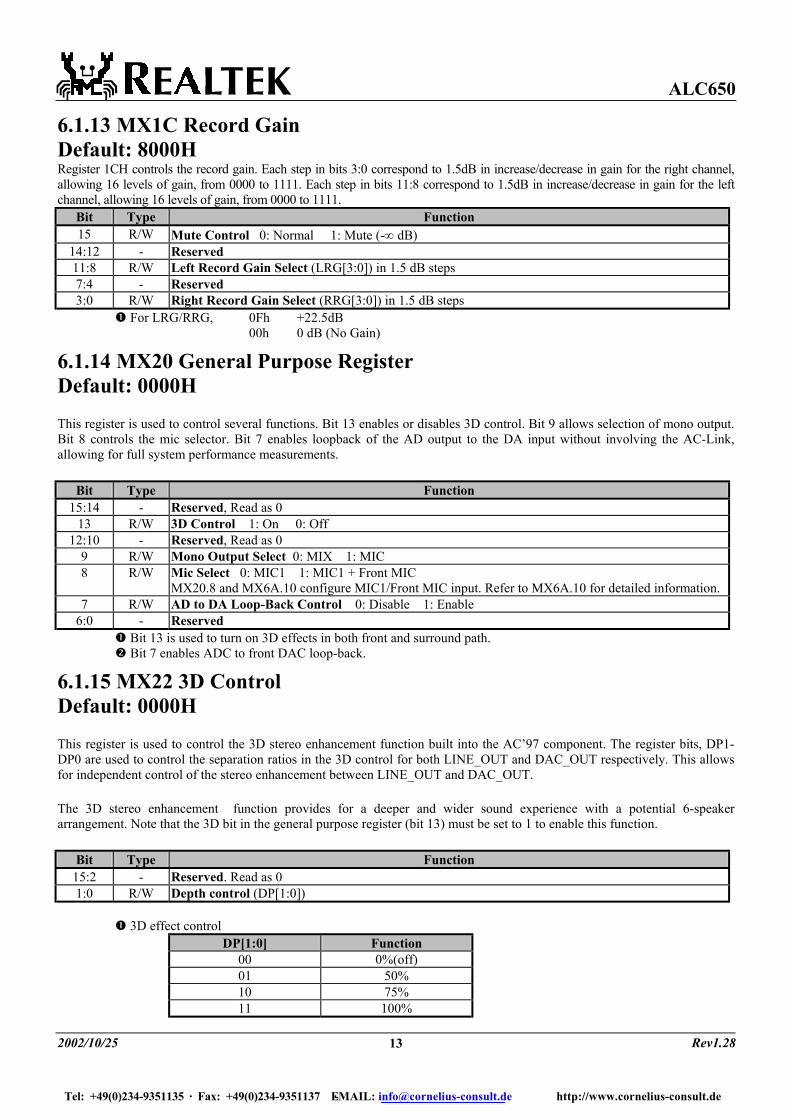
6.1.13 MX1C Record Gain Default: 8000H Register 1CH controls the record gain. Each step in bits 3:0 correspond to 1.5dB in increase/decrease in gain for the right channel, allowing 16 levels of gain, from 0000 to 1111. Each step in bits 11:8 correspond to 1.5dB in increase/decrease in gain for the left channel, allowing 16 levels of gain, from 0000 to 1111.
Bit Type Function 15 R/W Mute Control 0: Normal 1: Mute (-∞ dB)
14:12 - Reserved 11:8 R/W Left Record Gain Select (LRG[3:0]) in 1.5 dB steps 7:4 - Reserved 3:0 R/W Right Record Gain Select (RRG[3:0]) in 1.5 dB steps
For LRG/RRG, 0Fh +22.5dB 00h 0 dB (No Gain)
6.1.14 MX20 General Purpose Register Default: 0000H
This register is used to control several functions. Bit 13 enables or disables 3D control. Bit 9 allows selection of mono output. Bit 8 controls the mic selector. Bit 7 enables loopback of the AD output to the DA input without involving the AC-Link, allowing for full system performance measurements.
Bit Type Function 15:14 - Reserved, Read as 0
13 R/W 3D Control 1: On 0: Off 12:10 - Reserved, Read as 0
9 R/W Mono Output Select 0: MIX 1: MIC 8 R/W Mic Select 0: MIC1 1: MIC1 + Front MIC
MX20.8 and MX6A.10 configure MIC1/Front MIC input. Refer to MX6A.10 for detailed information. 7 R/W AD to DA Loop-Back Control 0: Disable 1: Enable
6:0 - Reserved Bit 13 is used to turn on 3D effects in both front and surround path. Bit 7 enables ADC to front DAC loop-back.
6.1.15 MX22 3D Control Default: 0000H
This register is used to control the 3D stereo enhancement function built into the AC’97 component. The register bits, DP1-DP0 are used to control the separation ratios in the 3D control for both LINE_OUT and DAC_OUT respectively. This allows for independent control of the stereo enhancement between LINE_OUT and DAC_OUT.
The 3D stereo enhancement function provides for a deeper and wider sound experience with a potential 6-speaker arrangement. Note that the 3D bit in the general purpose register (bit 13) must be set to 1 to enable this function.
Bit Type Function 15:2 - Reserved. Read as 0 1:0 R/W Depth control (DP[1:0])
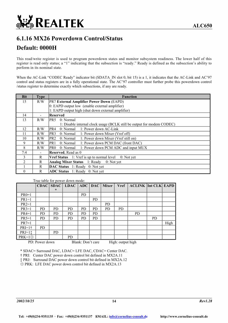
This read/write register is used to program powerdown states and monitor subsystem readiness. The lower half of this register is read only status; a “1” indicating that the subsection is “ready.” Ready is defined as the subsection’s ability to perform in its nominal state.
When the AC-Link “CODEC Ready” indicator bit (SDATA_IN slot 0, bit 15) is a 1, it indicates that the AC-Link and AC’97 control and status registers are in a fully operational state. The AC’97 controller must further probe this powerdown control /status register to determine exactly which subsections, if any are ready.
Bit Type Function 15 R/W PR7 External Amplifier Power Down (EAPD)
0: EAPD output low (enable external amplifier) 1: EAPD output high (shut down external amplifier)
14 - Reserved 13 R/W PR5 0: Normal
1: Disable internal clock usage (BCLK still be output for modem CODEC) 12 R/W PR4 0: Normal 1: Power down AC-Link 11 R/W PR3 0: Normal 1: Power down Mixer (Vref off) 10 R/W PR2 0: Normal 1: Power down Mixer (Vref still on) 9 R/W PR1 0: Normal 1: Power down PCM DAC (front DAC) 8 R/W PR0 0: Normal 1: Power down PCM ADC and input MUX
7:4 - Reserved, Read as 0 3 R Vref Status 1: Vref is up to normal level 0: Not yet 2 R Analog Mixer Status 1: Ready 0: Not yet 1 R DAC Status 1: Ready 0: Not yet 0 R ADC Status 1: Ready 0: Not yet
PRK=1 PD PD: Power down Blank: Don’t care High: output high
* SDAC= Surround DAC, LDAC= LFE DAC, CDAC= Center DAC. † PRI: Center DAC power down control bit defined in MX2A.11 ‡ PRJ: Surround DAC power down control bit defined in MX2A.12 PRK: LFE DAC power down control bit defined in MX2A.13
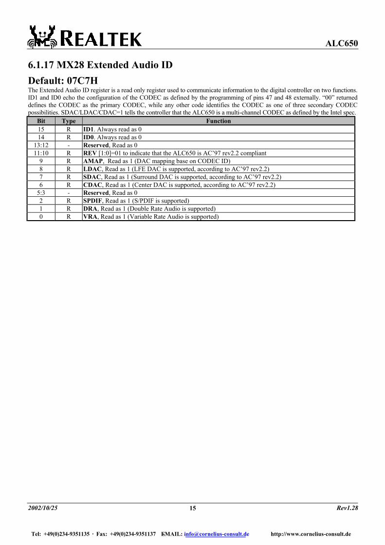
6.1.17 MX28 Extended Audio ID Default: 07C7H The Extended Audio ID register is a read only register used to communicate information to the digital controller on two functions. ID1 and ID0 echo the configuration of the CODEC as defined by the programming of pins 47 and 48 externally. “00” returned defines the CODEC as the primary CODEC, while any other code identifies the CODEC as one of three secondary CODEC possibilities. SDAC/LDAC/CDAC=1 tells the controller that the ALC650 is a multi-channel CODEC as defined by the Intel spec.
Bit Type Function 15 R ID1. Always read as 0 14 R ID0. Always read as 0
13:12 - Reserved, Read as 0 11:10 R REV [1:0]=01 to indicate that the ALC650 is AC’97 rev2.2 compliant
9 R AMAP, Read as 1 (DAC mapping base on CODEC ID) 8 R LDAC, Read as 1 (LFE DAC is supported, according to AC’97 rev2.2) 7 R SDAC, Read as 1 (Surround DAC is supported, according to AC’97 rev2.2) 6 R CDAC, Read as 1 (Center DAC is supported, according to AC’97 rev2.2)
5:3 - Reserved, Read as 0 2 R SPDIF, Read as 1 (S/PDIF is supported) 1 R DRA, Read as 1 (Double Rate Audio is supported) 0 R VRA, Read as 1 (Variable Rate Audio is supported)
6.1.18 MX2A Extended Audio Status and Control Register Default: 01F0H This register contains two active bits for powerdown and status of the surrounding DACs. Bits 0, 1 & 2 are read/write bits which are used to enable or disable VRA, DRA and SPDIF respectively. Bits 4 & 5 are read/write bits used to determine the AC-LINK slot assignment of the S/PDIF. Bits 6, 7 & 8 are read only bits which tell the controller when the Center, Surround and LFE DACs are ready to receive data. Bit 10 is a read only bit which tells the controller if the S/PDIF configuration is valid. Bits 11, 12 & 13 are read/write bits which are used to powerdown the Center, Surround and LFE DACs respectively.
Bit Type Function 15:14 - Reserved
13 R/W Power Down LFE DAC. (PRK) 0: Normal 1: Power down LFE DAC
12 R/W Power Down Surround DAC. (PRJ) 0: Normal 1: Power down Surround DAC
11 R/W Power Down Center DAC. (PRI) 0: Normal 1: Power down Center DAC
10 R SPCV (S/PDIF Configuration Valid) * 0: Current S/PDIF configuration SPSA,SPSR,DAC/slot rate is not valid 1: Current S/PDIF configuration SPSA,SPSR,DAC/slot rate is valid
9 - Reserved 8 R LFE DAC Status (LDAC). 0: Not yet 1: Ready † 7 R Surround DAC Status (SDAC). 0: Not yet 1: Ready † 6 R Center DAC Status (CDAC). 0: Not yet 1: Ready †
5:4 R/W SPSA[1:0] (S/PDIF Slot Assignment) 00: S/PDIF source data assigned to AC-LINK slot3/4 01: S/PDIF source data assigned to AC-LINK slot7/8 10: S/PDIF source data assigned to AC-LINK slot6/9 11: S/PDIF source data assigned to AC-LINK slot10/11 (default)
* SPCV is a read only bit that indicates whether the current S/PDIF configuration is supported or not. If the configuration is supported, SPCV is set as 1 by H/W. So driver can check this bit to determine the status of the S/PDIF transmitter system. SPCV is always operating, independent of the SPDIF enable bit (MX2A.2). The condition to allow S/PDIF output is SPDIF(MX2A.2)=1 & SPACV=1, otherwise the S/PDIF output will be all zero when MX2A.2=1 and SPACV=0 (invalid).
† Bit-13 (PRK), bit-12(PRJ), bit-11(PRI), bit-8(LDAC), bit-7 (SDAC) and bit-6(CDAC) are extended bits defined in AC’97 specification rev 2.1.
‡ Only front DACs supports 96KHz sample rate when DRA=1. MX2A.1 just selects clock source for front DACs. Software must set MX2C/MX2E/MX30 as BB80h, and mute surround DACs and CEN/LFE DACs. If VRA = 0, ALC650 AD/DA operate at fixed 48KHz sampling rate. Otherwise, it operates
with variable sampling rate defined in MX2C, MX2E, MX30 and MX32.
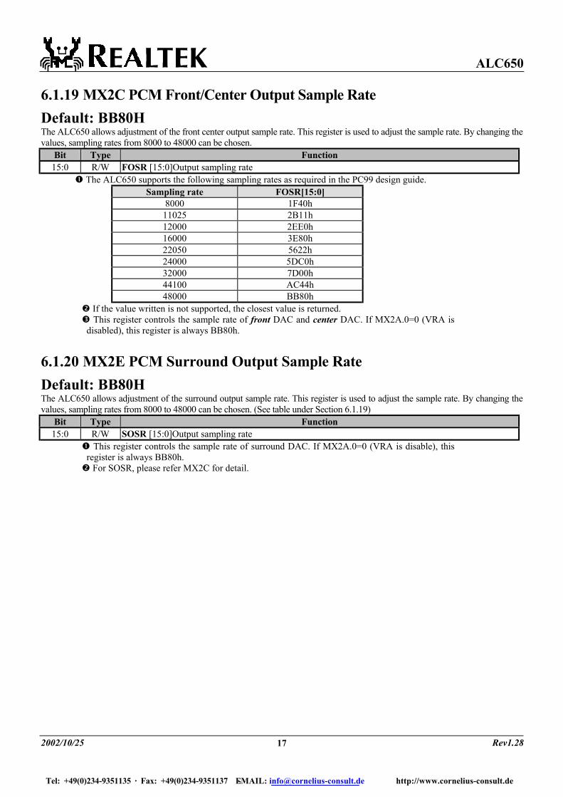
6.1.19 MX2C PCM Front/Center Output Sample Rate Default: BB80H The ALC650 allows adjustment of the front center output sample rate. This register is used to adjust the sample rate. By changing the values, sampling rates from 8000 to 48000 can be chosen.
Bit Type Function 15:0 R/W FOSR [15:0]Output sampling rate
The ALC650 supports the following sampling rates as required in the PC99 design guide. Sampling rate FOSR[15:0]
If the value written is not supported, the closest value is returned. This register controls the sample rate of front DAC and center DAC. If MX2A.0=0 (VRA is
disabled), this register is always BB80h.
6.1.20 MX2E PCM Surround Output Sample Rate Default: BB80H The ALC650 allows adjustment of the surround output sample rate. This register is used to adjust the sample rate. By changing the values, sampling rates from 8000 to 48000 can be chosen. (See table under Section 6.1.19)
Bit Type Function 15:0 R/W SOSR [15:0]Output sampling rate
This register controls the sample rate of surround DAC. If MX2A.0=0 (VRA is disable), this register is always BB80h. For SOSR, please refer MX2C for detail.
6.1.21 MX30 PCM LFE Output Sample Rate Default: BB80H The ALC650 allows adjustment of the PCM LFE output sample rate. This register is used to adjust the sample rate. By changing the values, sampling rates from 8000 to 48000 can be chosen. (See table under Section 6.1.19)
Bit Type Function 15:0 R/W LOSR [15:0]Output sampling rate
This register controls the sample rate of LFE DAC. If MX2A.0=0 (VRA is disable), this register is always BB80h. For LOSR, please refer MX2C for detail.
6.1.22 MX32 PCM Input Sample Rate Default: BB80H The ALC650 allows adjustment of the PCM input sample rate. This register is used to adjust the sample rate. By changing the values, sampling rates from 8000 to 48000 can be chosen.
Bit Type Function 15:0 R/W ISR [15:0]Output sampling rate
ALC650 support the following sampling rate required in PC99 design guide. Sampling rate ISR[15:0]
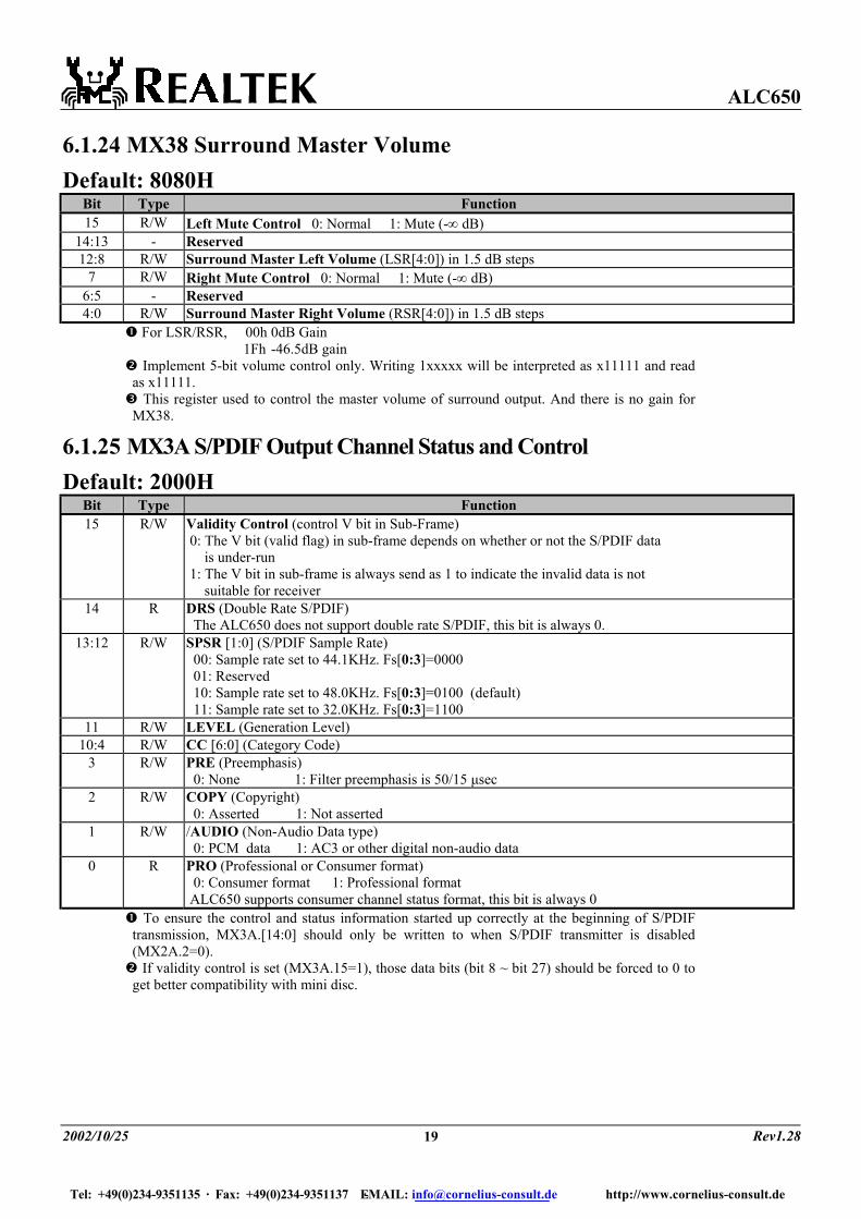
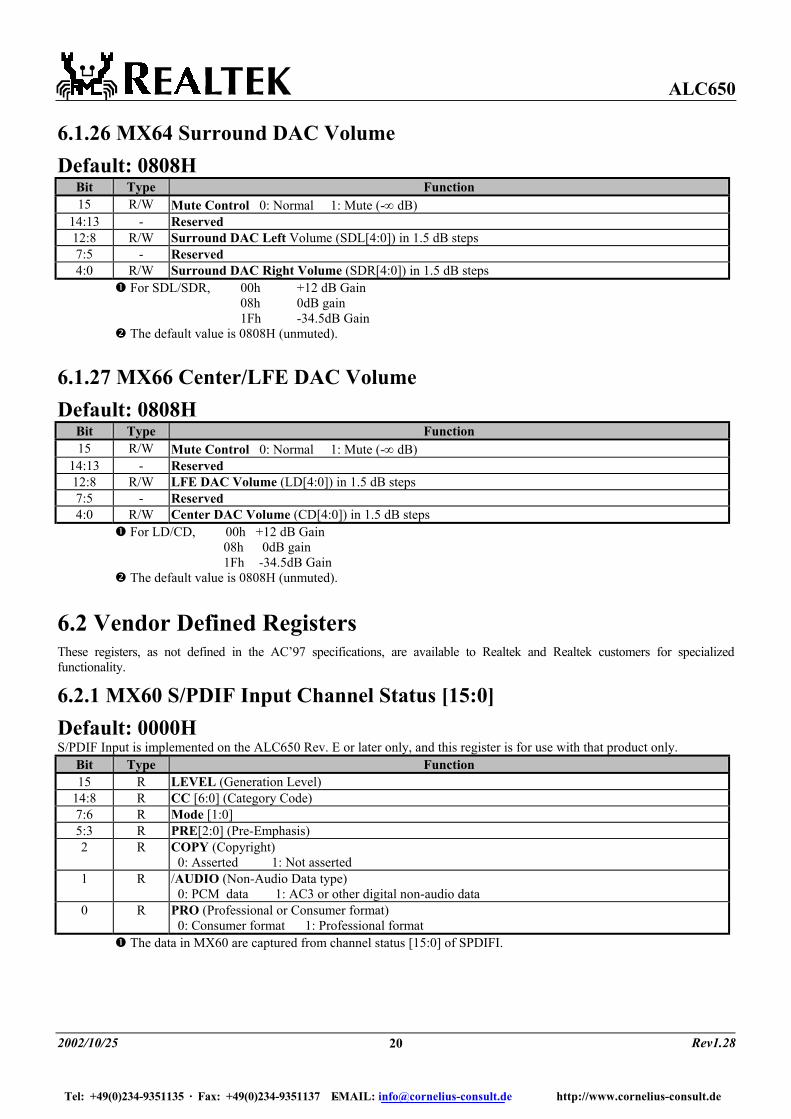
Bit Type Function 15 R/W LFE Mute Control 0: Normal 1: Mute (-∞ dB)
14:13 - Reserved 12:8 R/W LFE Master Volume (LFE[4:0]) in 1.5 dB steps
7 R/W Center Mute Control 0: Normal 1: Mute (-∞ dB) 6:5 - Reserved 4:0 R/W Center Master Volume (CNT[4:0]) in 1.5 dB steps
For LFE/CNT, 00h 0dB Gain 1Fh -46.5dB gain
Implement 5-bit volume control only. Writing 1xxxxx will be interpreted as x11111 and read as x11111. This register used to control the master volume of LFE and center output. And there is no gain
Bit Type Function 15 R/W Left Mute Control 0: Normal 1: Mute (-∞ dB)
14:13 - Reserved 12:8 R/W Surround Master Left Volume (LSR[4:0]) in 1.5 dB steps
7 R/W Right Mute Control 0: Normal 1: Mute (-∞ dB) 6:5 - Reserved 4:0 R/W Surround Master Right Volume (RSR[4:0]) in 1.5 dB steps
For LSR/RSR, 00h 0dB Gain 1Fh -46.5dB gain
Implement 5-bit volume control only. Writing 1xxxxx will be interpreted as x11111 and read as x11111. This register used to control the master volume of surround output. And there is no gain for
MX38.
6.1.25 MX3A S/PDIF Output Channel Status and Control Default: 2000H
Bit Type Function 15 R/W Validity Control (control V bit in Sub-Frame)
0: The V bit (valid flag) in sub-frame depends on whether or not the S/PDIF data is under-run 1: The V bit in sub-frame is always send as 1 to indicate the invalid data is not suitable for receiver
14 R DRS (Double Rate S/PDIF) The ALC650 does not support double rate S/PDIF, this bit is always 0.
13:12 R/W SPSR [1:0] (S/PDIF Sample Rate) 00: Sample rate set to 44.1KHz. Fs[0:3]=0000 01: Reserved 10: Sample rate set to 48.0KHz. Fs[0:3]=0100 (default) 11: Sample rate set to 32.0KHz. Fs[0:3]=1100
3 R/W PRE (Preemphasis) 0: None 1: Filter preemphasis is 50/15 µsec
2 R/W COPY (Copyright) 0: Asserted 1: Not asserted
1 R/W /AUDIO (Non-Audio Data type) 0: PCM data 1: AC3 or other digital non-audio data
0 R PRO (Professional or Consumer format) 0: Consumer format 1: Professional format ALC650 supports consumer channel status format, this bit is always 0
To ensure the control and status information started up correctly at the beginning of S/PDIF transmission, MX3A.[14:0] should only be written to when S/PDIF transmitter is disabled (MX2A.2=0). If validity control is set (MX3A.15=1), those data bits (bit 8 ~ bit 27) should be forced to 0 to
Bit Type Function 15 R/W Mute Control 0: Normal 1: Mute (-∞ dB)
14:13 - Reserved 12:8 R/W Surround DAC Left Volume (SDL[4:0]) in 1.5 dB steps 7:5 - Reserved 4:0 R/W Surround DAC Right Volume (SDR[4:0]) in 1.5 dB steps
For SDL/SDR, 00h +12 dB Gain 08h 0dB gain 1Fh -34.5dB Gain
The default value is 0808H (unmuted).
6.1.27 MX66 Center/LFE DAC Volume Default: 0808H
Bit Type Function 15 R/W Mute Control 0: Normal 1: Mute (-∞ dB)
14:13 - Reserved 12:8 R/W LFE DAC Volume (LD[4:0]) in 1.5 dB steps 7:5 - Reserved 4:0 R/W Center DAC Volume (CD[4:0]) in 1.5 dB steps
For LD/CD, 00h +12 dB Gain 08h 0dB gain 1Fh -34.5dB Gain
The default value is 0808H (unmuted).
6.2 Vendor Defined Registers These registers, as not defined in the AC’97 specifications, are available to Realtek and Realtek customers for specialized functionality.
6.2.1 MX60 S/PDIF Input Channel Status [15:0] Default: 0000H S/PDIF Input is implemented on the ALC650 Rev. E or later only, and this register is for use with that product only.
Bit Type Function 15 R LEVEL (Generation Level)
14:8 R CC [6:0] (Category Code) 7:6 R Mode [1:0] 5:3 R PRE[2:0] (Pre-Emphasis) 2 R COPY (Copyright)
0: Asserted 1: Not asserted 1 R /AUDIO (Non-Audio Data type)
0: PCM data 1: AC3 or other digital non-audio data 0 R PRO (Professional or Consumer format)
0: Consumer format 1: Professional format The data in MX60 are captured from channel status [15:0] of SPDIFI.
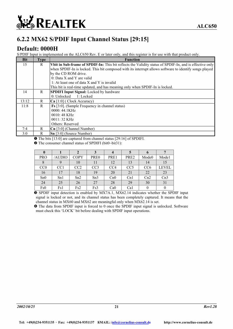
6.2.2 MX62 S/PDIF Input Channel Status [29:15] Default: 0000H S/PDIF Input is implemented on the ALC650 Rev. E or later only, and this register is for use with that product only.
Bit Type Function 15 R Vbit in Sub-frame of SPDIF-In: This bit reflects the Validity status of SPDIF-In, and is effective only
when SPDIF-In is locked. This bit composed with its interrupt allows software to identify songs played by the CD ROM drive. 0: Data X and Y are valid 1: At least one of data X and Y is invalid This bit is real-time updated, and has meaning only when SPDIF-In is locked.
14 R SPDIFI Input Signal: Locked by hardware 0: Unlocked 1: Locked
13:12 R Ca [1:0] ( Clock Accuracy) 11:8 R Fs [3:0]. (Sample Frequency in channel status)
SPDIF input detection is enabled by MX7A.1, MX62.14 indicates whether the SPDIF input signal is locked or not, and its channel status has been completely captured. It means that the channel status in MX60 and MX62 are meaningful only when MX62.14 is set. The data from SPDIF input is forced to 0 once the SPDIF input signal is unlocked. Software
must check this ‘LOCK’ bit before dealing with SPDIF input operations.
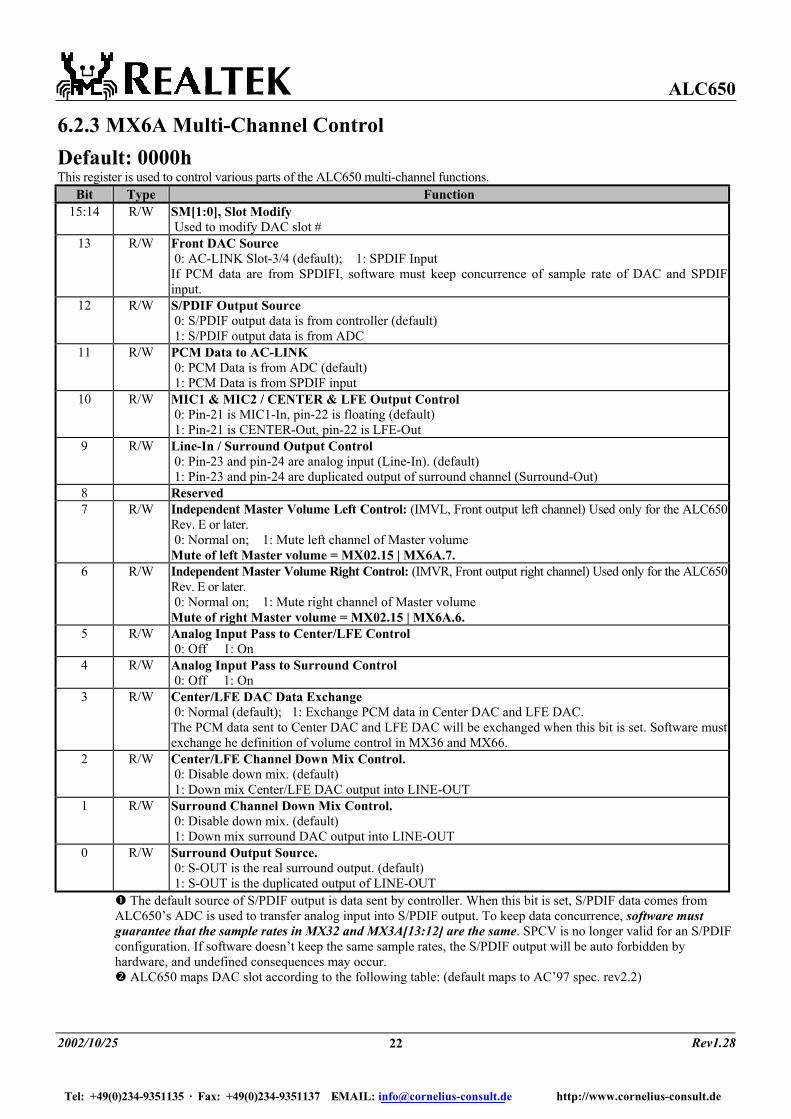
6.2.3 MX6A Multi-Channel Control Default: 0000h This register is used to control various parts of the ALC650 multi-channel functions.
Bit Type Function 15:14 R/W SM[1:0], Slot Modify
Used to modify DAC slot # 13 R/W Front DAC Source
0: AC-LINK Slot-3/4 (default); 1: SPDIF Input If PCM data are from SPDIFI, software must keep concurrence of sample rate of DAC and SPDIF input.
12 R/W S/PDIF Output Source 0: S/PDIF output data is from controller (default) 1: S/PDIF output data is from ADC
11 R/W PCM Data to AC-LINK 0: PCM Data is from ADC (default) 1: PCM Data is from SPDIF input
10 R/W MIC1 & MIC2 / CENTER & LFE Output Control 0: Pin-21 is MIC1-In, pin-22 is floating (default) 1: Pin-21 is CENTER-Out, pin-22 is LFE-Out
9 R/W Line-In / Surround Output Control 0: Pin-23 and pin-24 are analog input (Line-In). (default) 1: Pin-23 and pin-24 are duplicated output of surround channel (Surround-Out)
8 Reserved 7 R/W Independent Master Volume Left Control: (IMVL, Front output left channel) Used only for the ALC650
Rev. E or later. 0: Normal on; 1: Mute left channel of Master volume Mute of left Master volume = MX02.15 | MX6A.7.
6 R/W Independent Master Volume Right Control: (IMVR, Front output right channel) Used only for the ALC650 Rev. E or later. 0: Normal on; 1: Mute right channel of Master volume Mute of right Master volume = MX02.15 | MX6A.6.
5 R/W Analog Input Pass to Center/LFE Control 0: Off 1: On
4 R/W Analog Input Pass to Surround Control 0: Off 1: On
3 R/W Center/LFE DAC Data Exchange 0: Normal (default); 1: Exchange PCM data in Center DAC and LFE DAC. The PCM data sent to Center DAC and LFE DAC will be exchanged when this bit is set. Software must exchange he definition of volume control in MX36 and MX66.
2 R/W Center/LFE Channel Down Mix Control. 0: Disable down mix. (default) 1: Down mix Center/LFE DAC output into LINE-OUT
1 R/W Surround Channel Down Mix Control. 0: Disable down mix. (default) 1: Down mix surround DAC output into LINE-OUT
0 R/W Surround Output Source. 0: S-OUT is the real surround output. (default) 1: S-OUT is the duplicated output of LINE-OUT
The default source of S/PDIF output is data sent by controller. When this bit is set, S/PDIF data comes from ALC650’s ADC is used to transfer analog input into S/PDIF output. To keep data concurrence, software must guarantee that the sample rates in MX32 and MX3A[13:12] are the same. SPCV is no longer valid for an S/PDIF configuration. If software doesn’t keep the same sample rates, the S/PDIF output will be auto forbidden by hardware, and undefined consequences may occur.
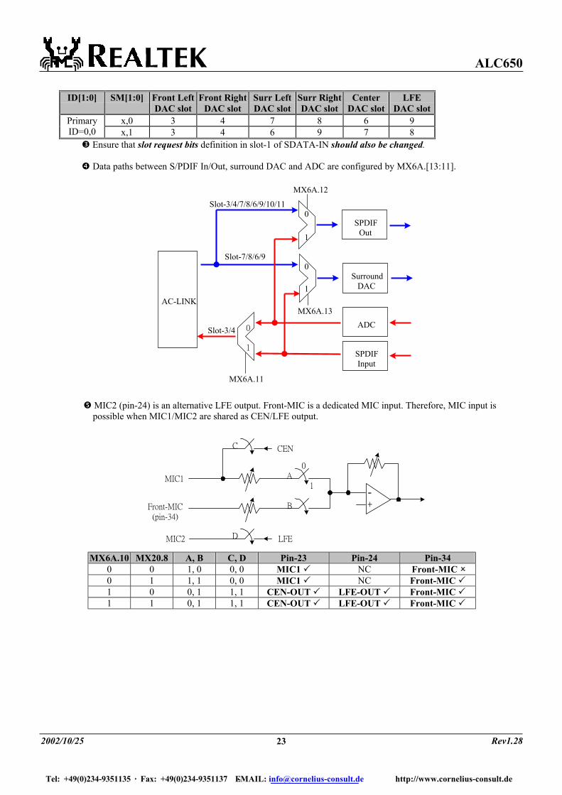
ALC650 maps DAC slot according to the following table: (default maps to AC’97 spec. rev2.2)
Ensure that slot request bits definition in slot-1 of SDATA-IN should also be changed.
Data paths between S/PDIF In/Out, surround DAC and ADC are configured by MX6A.[13:11].
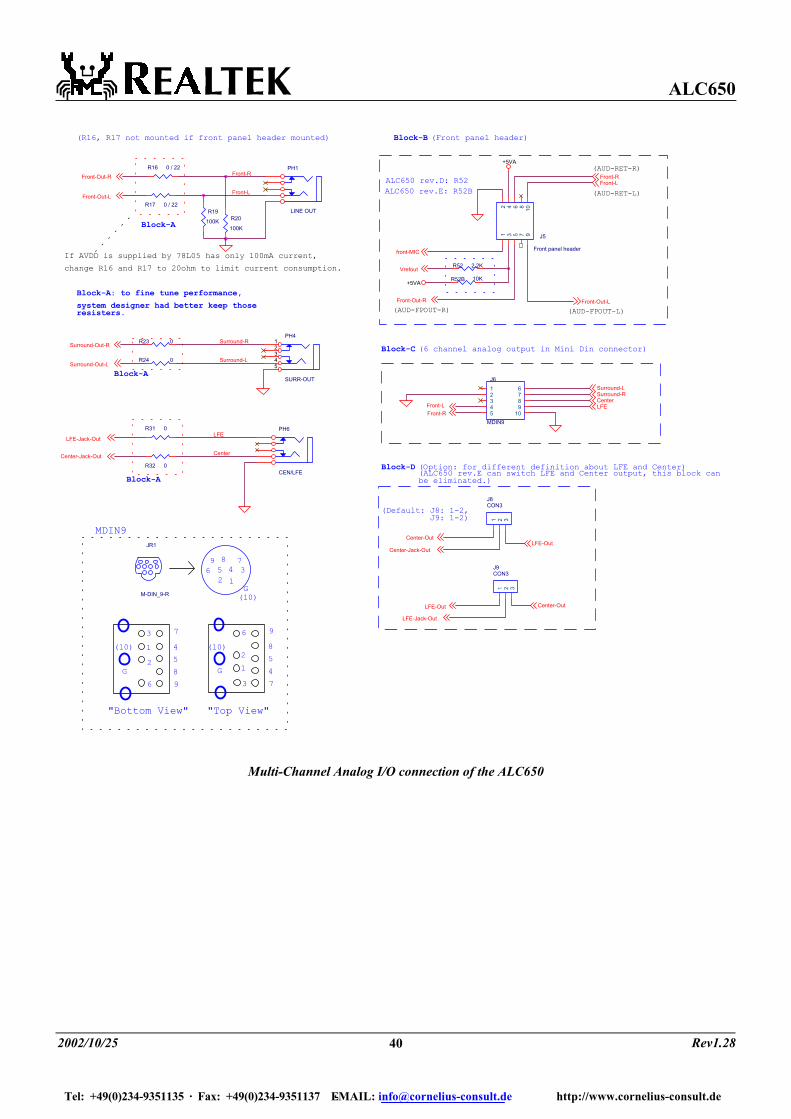
MIC2 (pin-24) is an alternative LFE output. Front-MIC is a dedicated MIC input. Therefore, MIC input is possible when MIC1/MIC2 are shared as CEN/LFE output.
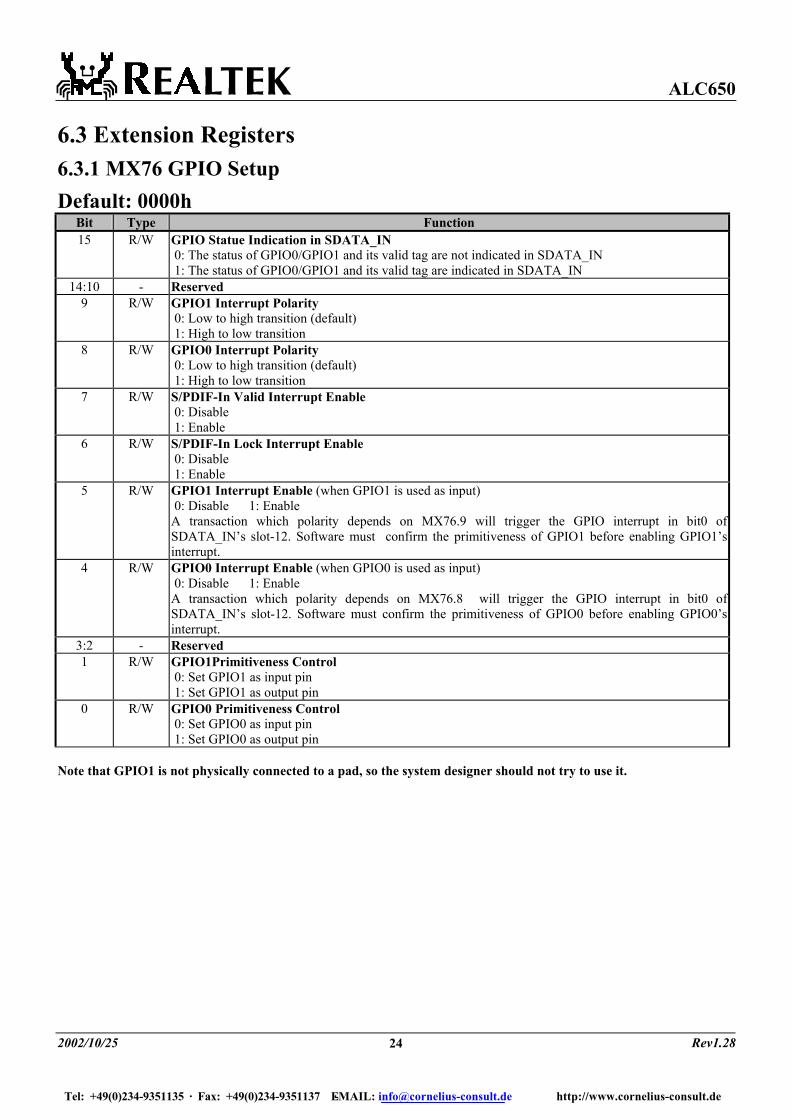
5 R/W GPIO1 Interrupt Enable (when GPIO1 is used as input) 0: Disable 1: Enable A transaction which polarity depends on MX76.9 will trigger the GPIO interrupt in bit0 of SDATA_IN’s slot-12. Software must confirm the primitiveness of GPIO1 before enabling GPIO1’s interrupt.
4 R/W GPIO0 Interrupt Enable (when GPIO0 is used as input) 0: Disable 1: Enable A transaction which polarity depends on MX76.8 will trigger the GPIO interrupt in bit0 of SDATA_IN’s slot-12. Software must confirm the primitiveness of GPIO0 before enabling GPIO0’s interrupt.
3:2 - Reserved 1 R/W GPIO1Primitiveness Control
0: Set GPIO1 as input pin 1: Set GPIO1 as output pin
0 R/W GPIO0 Primitiveness Control 0: Set GPIO0 as input pin 1: Set GPIO0 as output pin
Note that GPIO1 is not physically connected to a pad, so the system designer should not try to use it.
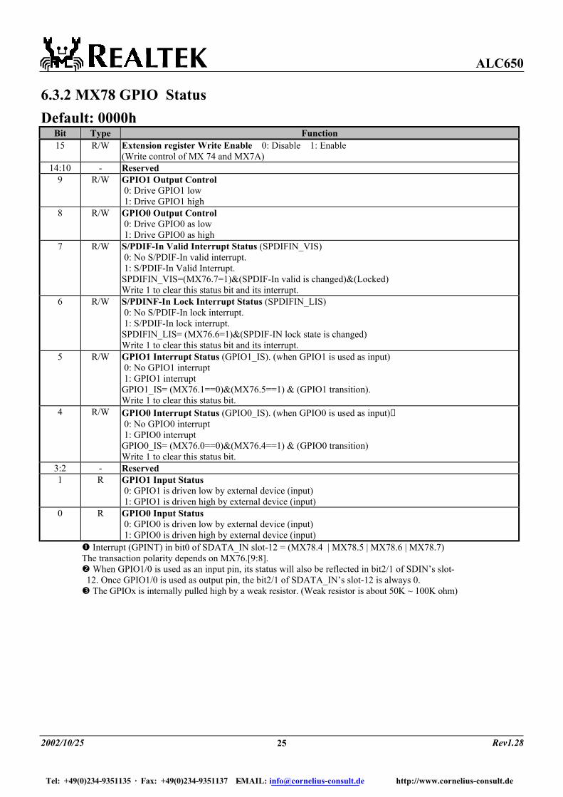
Bit Type Function 15 R/W Extension register Write Enable 0: Disable 1: Enable
(Write control of MX 74 and MX7A) 14:10 - Reserved
9 R/W GPIO1 Output Control 0: Drive GPIO1 low 1: Drive GPIO1 high
8 R/W GPIO0 Output Control 0: Drive GPIO0 as low 1: Drive GPIO0 as high
7 R/W S/PDIF-In Valid Interrupt Status (SPDIFIN_VIS) 0: No S/PDIF-In valid interrupt. 1: S/PDIF-In Valid Interrupt. SPDIFIN_VIS=(MX76.7=1)&(SPDIF-In valid is changed)&(Locked) Write 1 to clear this status bit and its interrupt.
6 R/W S/PDINF-In Lock Interrupt Status (SPDIFIN_LIS) 0: No S/PDIF-In lock interrupt. 1: S/PDIF-In lock interrupt. SPDIFIN_LIS= (MX76.6=1)&(SPDIF-IN lock state is changed) Write 1 to clear this status bit and its interrupt.
5 R/W GPIO1 Interrupt Status (GPIO1_IS). (when GPIO1 is used as input) 0: No GPIO1 interrupt 1: GPIO1 interrupt GPIO1_IS= (MX76.1==0)&(MX76.5==1) & (GPIO1 transition). Write 1 to clear this status bit.
4 R/W GPIO0 Interrupt Status (GPIO0_IS). (when GPIO0 is used as input)❶ 0: No GPIO0 interrupt 1: GPIO0 interrupt GPIO0_IS= (MX76.0==0)&(MX76.4==1) & (GPIO0 transition) Write 1 to clear this status bit.
3:2 - Reserved 1 R GPIO1 Input Status
0: GPIO1 is driven low by external device (input) 1: GPIO1 is driven high by external device (input)
0 R GPIO0 Input Status 0: GPIO0 is driven low by external device (input) 1: GPIO0 is driven high by external device (input)
Interrupt (GPINT) in bit0 of SDATA_IN slot-12 = (MX78.4 | MX78.5 | MX78.6 | MX78.7) The transaction polarity depends on MX76.[9:8].
When GPIO1/0 is used as an input pin, its status will also be reflected in bit2/1 of SDIN’s slot-12. Once GPIO1/0 is used as output pin, the bit2/1 of SDATA_IN’s slot-12 is always 0. The GPIOx is internally pulled high by a weak resistor. (Weak resistor is about 50K ~ 100K ohm)
6.3.3 MX7A Clock Source, Pin-47, S/PDIF Input Receiver Default: 0002H This register is used for three types of information. Bit 0 is a read/write bit which enables/disables the S/PDIF input receiver. Bit 1 is used to switch pin 47, which is duplexed due for pin-count reduction, between EAPD and S/PDIF modes. Bit 2 is used to select the clock source for the ALC650.
Bit Type Function 15:3 - Reserved
2 R Clock Source Selection (XTLSEL) 0: Bypass 14.318M 24.576M digital PLL. (Default if XTSEL is floating) 1: Select 14.318M 24.576M digital PLL. (Default if XTLSEL is pull low)
1 R/W Pin-47 Control: This bit determines the function of Pin 47, a multiplexed pin. 0: EAPD (output) 1: S/PDIF Input (input) – The S/PDIF-In function is only supported by the ALC650 Rev. E or later.
0 R/W Enable S/PDIF Input Receiver 0: Disable 1: Enable – The S/PDIF-In function is only supported by ALC650 Rev. E or later.
6.3.4 MX7C VENDOR ID1 Default: 414CH
The two registers (MX7C Vendor ID1 and MX7E Vendor ID2) contain four 8-bit ID codes. The first three codes have been assigned by Microsoft for Plug and Play definitions. The fourth code is a Realtek assigned code identifying the ALC650. The MX7C Vendor ID1 register contains the value 414Ch, which is the first and second characters of the Microsoft ID code. The MX7C Vendor ID2 register contains the value 4720h, which is the third of the Microsoft ID code.
Bit Type Function 15:0 R Vendor ID “AL”
6.3.5 MX7E VENDOR ID2 Default: 4720H
Bit Type Function 15:8 R Vendor ID “G” 7:4 R Chip ID 0010 3:0 R Version number 00: version A
For WHQL issue, Here version number is always 0. Chip ID 0010 ALC650
6.3.6 MX74 MISCELLANEOUS CONTROL Default: 0043H
Bit Type Function 15:14 - Reserved
13 R/W Ignore V bit in sub-frame of SPDIF-IN (Supported by the ALC650 Rev. F) 0: Disable, SPDIF-IN FIFO will keep the last valid data. (default) 1: Enable, SPDIF-IN FIFO will catch the SPDIF-In data in spite of the V bit.
12 R/W Vrefout Disable (Supported by the ALC650 Rev. E and Rev.F) 0: Vrefout is driven by the internal reference (Default) 1: Vrefout is in high-Z mode. Software must set this bit to disable Vrefout output before MX6A.10 is set (MIC1 and MIC2 are shared
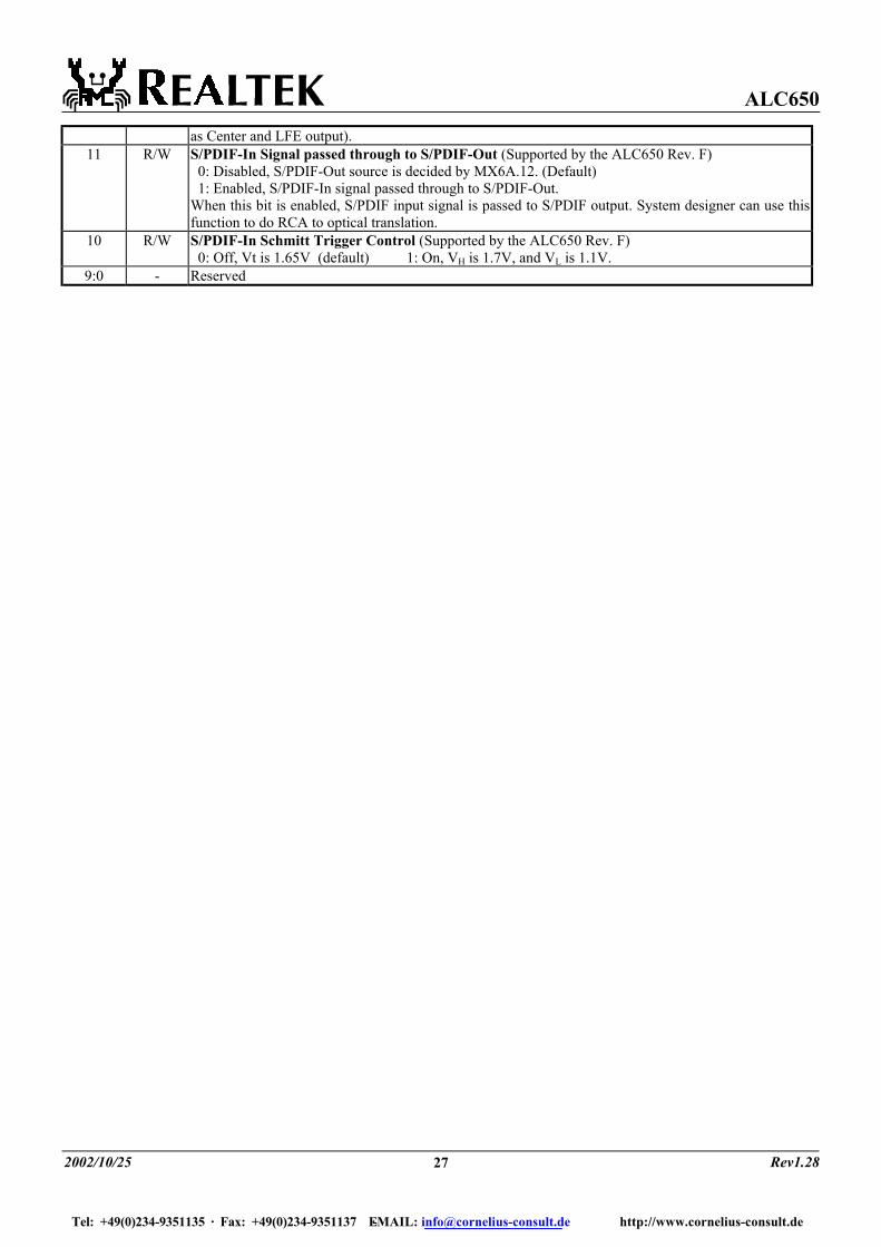
as Center and LFE output). 11 R/W S/PDIF-In Signal passed through to S/PDIF-Out (Supported by the ALC650 Rev. F)
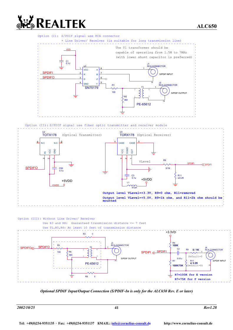
0: Disabled, S/PDIF-Out source is decided by MX6A.12. (Default) 1: Enabled, S/PDIF-In signal passed through to S/PDIF-Out. When this bit is enabled, S/PDIF input signal is passed to S/PDIF output. System designer can use this function to do RCA to optical translation.
10 R/W S/PDIF-In Schmitt Trigger Control (Supported by the ALC650 Rev. F) 0: Off, Vt is 1.65V (default) 1: On, VH is 1.7V, and VL is 1.1V.
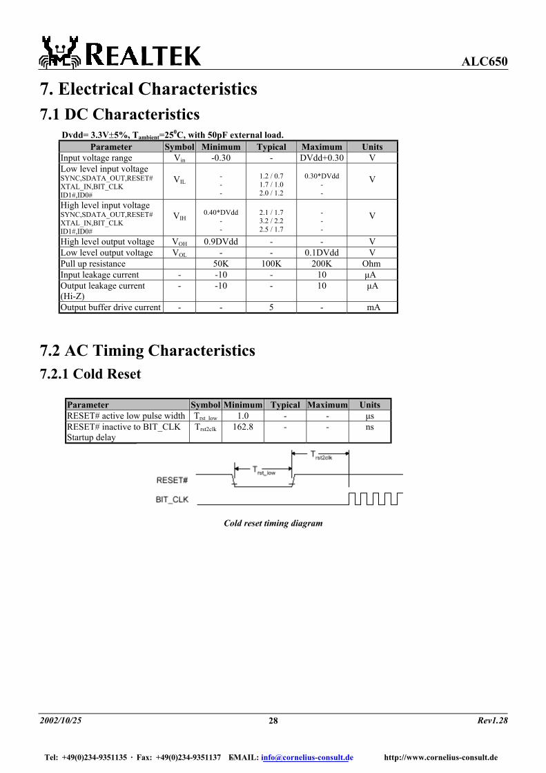
7. Electrical Characteristics 7.1 DC Characteristics
Dvdd= 3.3V±5%, Tambient=250C, with 50pF external load. Parameter Symbol Minimum Typical Maximum Units
Input voltage range Vin -0.30 - DVdd+0.30 V Low level input voltage SYNC,SDATA_OUT,RESET# XTAL_IN,BIT_CLK ID1#,ID0#
VIL
- - -
1.2 / 0.7 1.7 / 1.0 2.0 / 1.2
0.30*DVdd
- -
V
High level input voltage SYNC,SDATA_OUT,RESET# XTAL_IN,BIT_CLK ID1#,ID0#
VIH
0.40*DVdd
- -
2.1 / 1.7 3.2 / 2.2 2.5 / 1.7
- - -
V
High level output voltage VOH 0.9DVdd - - V Low level output voltage VOL - - 0.1DVdd V Pull up resistance 50K 100K 200K Ohm Input leakage current - -10 - 10 µA Output leakage current (Hi-Z)
- -10 - 10 µA
Output buffer drive current - - 5 - mA
7.2 AC Timing Characteristics 7.2.1 Cold Reset
Parameter Symbol Minimum Typical Maximum Units RESET# active low pulse width Trst_low 1.0 - - µs RESET# inactive to BIT_CLK Startup delay
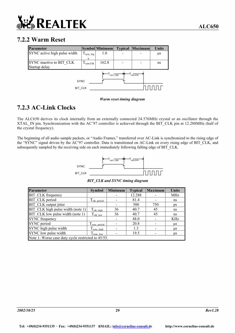
7.2.2 Warm Reset Parameter Symbol Minimum Typical Maximum Units SYNC active high pulse width Tsync_hig
h
1.0 - - µs
SYNC inactive to BIT_CLK Startup delay
Tsync2clk 162.8 - - ns
Warm reset timing diagram
7.2.3 AC-Link Clocks
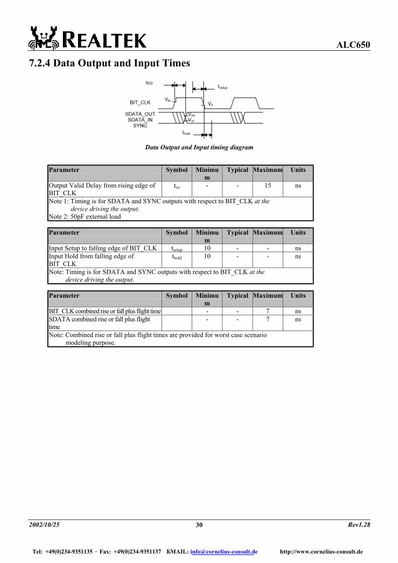
The ALC650 derives its clock internally from an externally connected 24.576MHz crystal or an oscillator through the XTAL_IN pin. Synchronization with the AC’97 controller is achieved through the BIT_CLK pin at 12.288MHz (half of the crystal frequency).
The beginning of all audio sample packets, or “Audio Frames,” transferred over AC-Link is synchronized to the rising edge of the “SYNC” signal driven by the AC’97 controller. Data is transitioned on AC-Link on every rising edge of BIT_CLK, and subsequently sampled by the receiving side on each immediately following falling edge of BIT_CLK.
BIT_CLK and SYNC timing diagram
Parameter Symbol Minimum Typical Maximum Units BIT_CLK frequency - 12.288 - MHz BIT_CLK period Tclk_period - 81.4 - ns BIT_CLK output jitter - 500 750 ps BIT_CLK high pulse width (note 1) Tclk_high 36 40.7 45 ns BIT_CLK low pulse width (note 1) Tclk_low 36 40.7 45 ns SYNC frequency - 48.0 - KHz SYNC period Tsync_period - 20.8 - µs SYNC high pulse width Tsync_high - 1.3 - µs SYNC low pulse width Tsync_low - 19.5 - µs Note 1: Worse case duty cycle restricted to 45/55.
Parameter Symbol Minimum Typical Maximum Units BIT_CLK rise time Triseclk - - 6 ns BIT_CLK fall time Tfallclk - - 6 ns SYNC rise time Trisesync - - 6 ns SYNC fall time Tfallsync - - 6 ns SDATA_IN rise time Trisedin - - 6 ns SDATA_IN fall time Tfalldin - - 6 ns SDATA_OUT rise time Trisedout - - 6 ns SDATA_OUT fall time Tfalldout - - 6 ns Note 1: 75pF external load Note 2: rise is from 10% to 90% of Vdd (Vol to Voh) Note 3: fall is from 90% to 10% of Vdd (Voh to Vol)
7.2.6 AC-Link Low Power Mode Timing The ALC650 AC-Link can be placed into low power mode by programming register 26h. Both BIT_CLK and SDATA_IN will be brought to and held at a logic low voltage level. The AC’97 controller can wake up the ALC650 by providing the proper reset signals.
AC-Link low power mode timing diagram
Parameter Symbol Minimum Typical Maximum Units End of slot 2 to BIT_CLK, SDATA_IN low
Ts2_pdown - - 1.0 µs
BIT_CLK and SDATA_IN are transitioned low immediately (within the maximum specified time) following the decode of the write to the Powerdown register (26h) with PR4. When the AC’97 controller driver is at the point where it is ready to program the AC-Link into its low power mode, slots 1 and 2 are assumed to be the only valid stream in the audio output frame after all audio sources have been neutralized. The AC’97 controller should also drive SYNC and SDATA_OUT low after changing the ALC650 to low power mode.
7.2.7 ATE Test Mode
ATE test mode timing diagram
*To meet AC’97 Rev.2.2 requirements, EAPD, SPDIFO, BIT_CLK and SDATA_IN should be floating in test mode.
Parameter Symbol Minimum Typical Maximum Units Setup to trailing edge of RESET# (also applies to SYNC)
Tsetup2rst 15.0 - - ns
Rising edge of RESET# to Hi-Z delay Toff - - 25.0 ns
All AC-Link signals are normally low through the trailing edge of RESET#. Asserting SDATA_OUT high for the trailing edge of RESET# causes the AC-Link outputs of the ALC650 to go to high impedance, which is suitable for ATE in circuit testing. Once either of the two test modes have been entered, the ALC650 must be issued another RESET# with all AC-Link signals low to return to normal operating mode.
7.2.9 SPDIF Output SPDIF_OUT Minimum Typical Maximum Unit
Rise time/fall time 0 10 % Duty cycle 45 55 %
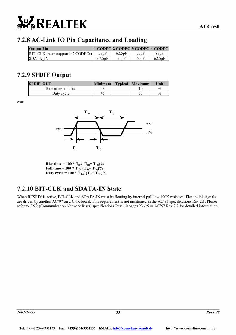
Note:
T(h) T(l)
T(r) T(f)
90%50%
10%
Rise time = 100 * T(r)/ (T(l)+ T(h))% Fall time = 100 * T(f)/ (T(l)+ T(h))% Duty cycle = 100 * T(h)/ (T(l)+ T(h))%
7.2.10 BIT-CLK and SDATA-IN State When RESET# is active, BIT-CLK and SDATA-IN must be floating by internal pull low 100K resistors. The ac-link signals are driven by another AC’97 on a CNR board. This requirement is not mentioned in the AC’97 specifications Rev 2.1. Please refer to CNR (Communication Network Riser) specifications Rev.1.0 pages 23~25 or AC’97 Rev.2.2 for detailed information.
8. Analog Performance Characteristics Standard test condition: Tambient=250C, Dvdd=5.0 or 3.3V ±5%,Avdd=5.0V±5% Input Voltage Level: Logic Low=0.35*Vdd, Logic High=0.65Vdd 1KHz input sine wave; Sampling frequency=48KHz; 0dB=1Vrms 10KΩ/50pF load; Test bench characterization BW:20Hz~20KHz 0dB attenuation; tone and 3D disabled Parameter Minimum Typical Maximum Units Full scale input voltage Mixer (except for MIC) Mic input (gain=0dB) Mic input (gain=20dB) ADC
- - - -
1.6 1.6
0.16 1.0
- - - -
Vrms Vrms Vrms Vrms
Full scale output voltage Front DAC Front DAC (F version) Surround DAC, Center/LFE DAC
- - -
1.5 1.1 1.1
- - -
Vrms Vrms Vrms
S/N (A weighted) Analog Inputs to LINE_OUT ADC DAC (Front DAC with headphone amp) DAC (Surround, Center, LFE DAC)
- - - -
95 85 85 90
- - - -
dB FSA dB FSA dB FSA dB FSA
THD+N Analog Inputs to LINE_OUT ADC DAC (Front DAC with headphone amp) DAC (Surround, Center, LFE DAC)
- - - -
-85 -80 -75 -80
- - - -
dB FS dB FS dB FS dB FS
Frequency Response Mixers ADC, DAC
10 16
- -
22,000 19,200
Hz Hz
Power Supply Rejection (DAC, ADC) - -68 - dB Total Out-of-Band Noise (28.8K~100KHz) - -63 - dB Mic 20dB gain is selected 18 20 22 dB Crosstalk between inputs channels - -70 dB Attenuation, Gain Step Size - 1.5 - dB Input impedance (gain=0dB) MIC1, MIC2, PCBEEP, PHONE Others (LINE,CD,AUX,VIDEO) ADC
- - -
16 32 32
- - -
KΩ KΩ KΩ
Power Supply Current (normal operation) VA=5V / VD=3.3V VA=3.3V / VD=3.3V
- -
88 / 36 71 / 36
- -
mA
Power Supply Current (power down mode) VA=5V / VD=3.3V VA=3.3V / VD=3.3V
- -
0.5 / 10 0.2 / 10
- -
mA
Vrefout 2.25 2.50 2.75 V Digital Filter Characteristics ADC Lowpass Filter Passband Stopband Stopband Rejection Passband Frequency Response
0
28.8 - -
- -
-76.0 +- 0.15
19.2
- - -
KHz KHz dB dB
DAC Lowpass Filter Passband Stopband Stopband Rejection Passband Frequency Response
9.2 AC-Link When the ALC650 takes serial data from the AC’97 controller, it samples SDATA_OUT on the falling edge of BIT_CLK. When the ALC650 sends serial data to the AC’97 controller, it starts to drive SDATA_IN on the rising edge of BIT_CLK.
The ALC650 will return any uninstalled bits or registers with 0 for the read operation. The ALC650 also stuffs the unimplemented slot or bit with 0 in SDATA-IN. Note that AC-LINK is MSB-justified.
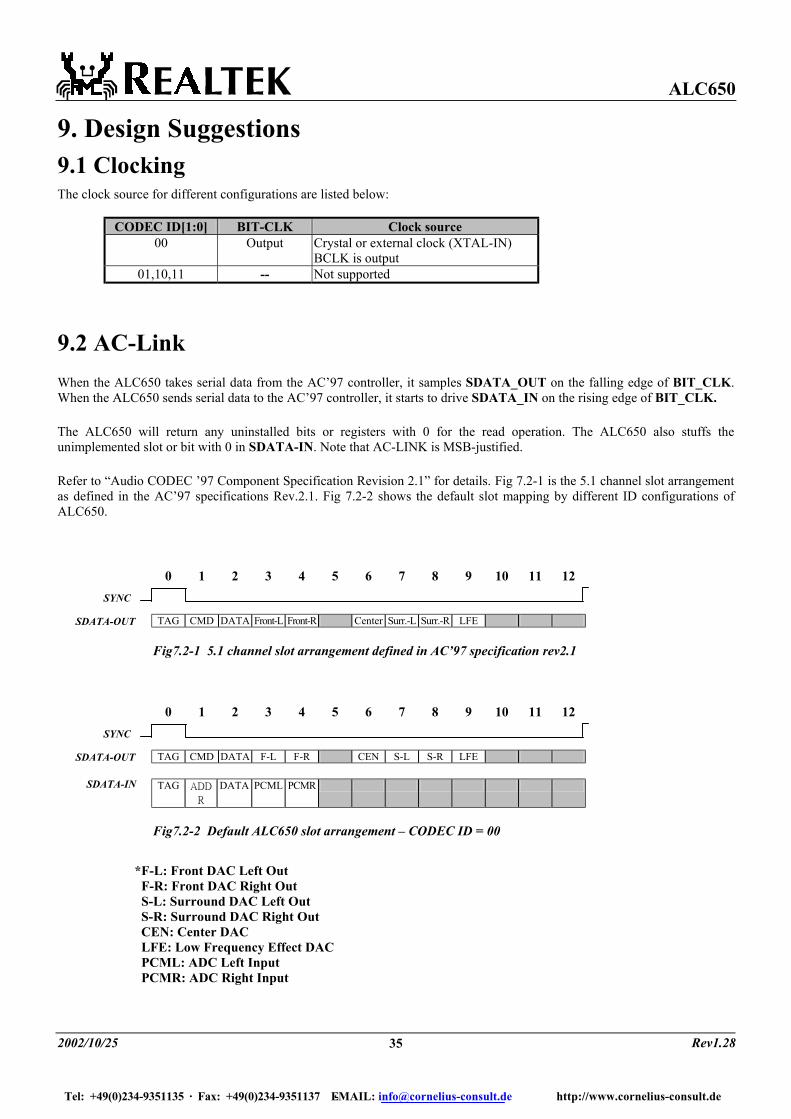
Refer to “Audio CODEC ’97 Component Specification Revision 2.1” for details. Fig 7.2-1 is the 5.1 channel slot arrangement as defined in the AC’97 specifications Rev.2.1. Fig 7.2-2 shows the default slot mapping by different ID configurations of ALC650.
0 1 2 3 4 5 6 7 8 9 10 11 12
TAG CMD DATA Front-L Front-R Center Surr.-L Surr.-R LFE Fig7.2-1 5.1 channel slot arrangement defined in AC’97 specification rev2.1
0 1 2 3 4 5 6 7 8 9 10 11 12
TAG CMD DATA F-L F-R CEN S-L S-R LFE
TAG ADD
R
DATA PCML PCMR
Fig7.2-2 Default ALC650 slot arrangement – CODEC ID = 00 *F-L: Front DAC Left Out F-R: Front DAC Right Out S-L: Surround DAC Left Out S-R: Surround DAC Right Out CEN: Center DAC LFE: Low Frequency Effect DAC PCML: ADC Left Input PCMR: ADC Right Input
9.6 Power-down Mode Pay special attention to powerdown control register (index 26h), especially PR4 (power-down AC-link)
Example of ALC650 power-down/power-up flow
9.7 Test Mode The ALC650 has two test modes. One is for ATE in circuit test and the other is for vendor specific tests. All AC-link signals are normally low through the trailing edge of RESET#. When coming out of RESET, an AC’97 CODEC enters the ATE in circuit test mode if SDATA_OUT is sampled high at the trailing edge of RESET#, and enters the vendor specific test mode if SYNC is sampled high at the trailing edge of RESET#. Note that the ALC650 Rev. E does not support vendor specific test mode.
These cases will never occur during standard operating conditions.
Regardless of the test mode, the ALC650 will issue a cold reset to resume normal operation.
SYNC SDATA_OUT Description 0 0 Normal operation 0 1 ATE Test Mode 1 0 Vendor Test Mode 1 1 Reserved
9.7.1 ATE In Circuit Test Mode SDATA_OUT is sampled high at the trailing edge of RESET#. In this mode, the ALC650 will drive BIT_CLK, SDATA_IN, EAPD and SPDIFO to high impedance.
9.7.2 Vendor Specific Test Mode SYNC is sampled high at the trailing edge of RESET#. In this mode, the ALC650 will drive BIT_CLK, SDATA_IN, EAPD and SPDIFO to high impedance. Note: To attain closest compatibility with AC’97 rev2.2, the ALC650 will float its digital output pins in both ATE and
Vendor-Specific test modes. Please refer to AC’97 rev2.2 section 9.2 for detail description about test mode.
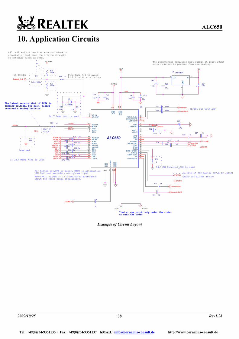
The recommended regulator must supply at least 200mAoutput current to prevent from overheating.
Fine tune R48 to avoidkink from external clock
R47, R49 and C14 can bias external clock toacceptable level once the driving strengthof external clock is weak.
Tied at one point only under the codecor near the codec
DGND AGND
(EAPD for ALC650 rev.D)
For ALC650 rev.D/E or later, MIC2 is alternativeLFE-Out, not secondary microphone input.Front-MIC at pin 34 is a dedicated microphoneinput for front panel application.
if 24.576MHz XTAL is used
The latest version (Bx) of ICH4 istimeing critical for SDIN, pleasereserved a series resistor