ALD deposited ferroelectric HfO 2 S. Slesazeck 1 , U. Schroeder 1 , E. Yurchuk 1 , J. Müller 2 , S. Müller 1 , D. Martin 1 , T. Schenk 1 , C. Richter 1 ,C. Adelmann 3 , S. Kalinin 5 , A. Kersch 7 , and T. Mikolajick 1,4 3rd ALD Symposium - SEMICON Europa October 7 th 2014 1 October 7 th , 2014 1 3 2 6 5 7
Transcript
ALD deposited ferroelectric HfO2
S. Slesazeck1, U. Schroeder1, E. Yurchuk1, J. Müller2, S. Müller1, D. Martin1, T. Schenk1,
C. Richter1,C. Adelmann3, S. Kalinin5, A. Kersch7, and T. Mikolajick1,4
3rd ALD Symposium - SEMICON Europa
October 7th 2014
1
October 7th, 2014
132 65 7
Outline
2. Stabilization of the Ferroelectric HfO2 Phase
1. Motivation: Ferroelectricity in HfO2
3. Device Application: 1T FeFET Memory
4. Summary
2S. Slesazeck et al.
SEMICON 10/2014 Grenoble
Outline
2. Stabilization of the Ferroelectric HfO2 Phase
1. Motivation: Ferroelectricity in HfO2
3. Device Application: 1T FeFET
4. Summary
3S. Slesazeck et al.
SEMICON 10/2014 Grenoble
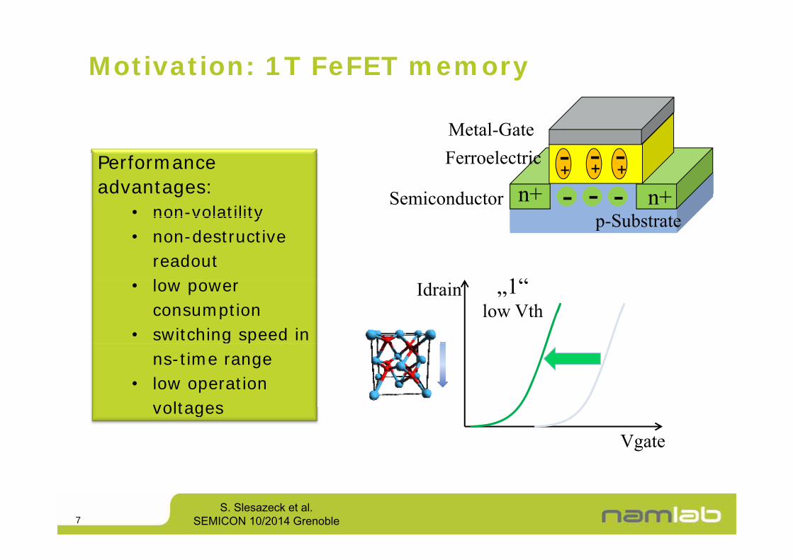
Motivation: Ferroelectric HfO2
Ferroelectrics enablefast low power non-volatile memories
130nm FRAMp
e.g. FRAM:- current scaling limit: 130 nm
due to material properties new material necessary
TI & Ramtron
A lot of industry experienceintegrating HfO2 / ZrO2:
CMOS DRAMsub 30 nm
g g 2 2
- CMOS compatible- scalability well below 50nm- ALD process available- ferroelectric properties
- Phase: Polarization direction detectable- Local distribution
D Martin @ Oak Ridge Nat Labs
25S. Slesazeck et al.
SEMICON 10/2014 Grenoble
D. Martin @ Oak Ridge Nat. Labs
Piezo Force Measurements
180°3
+4.2 V0°
a.u.nm3nm
2
-4.2 V0°
1
Topography Piezo responce Phase
-180°0
- Most HfO2 grains switchable
polarization value visible two polarization direction
D. Martin et al., Ad M tMost HfO2 grains switchable
- PFM serves as base for optimization of film composition
and crystallization on simple capacitor structures
Adv. Mat.submitted
U. Schroeder et al., IWDTF 2013/ JJAP 2014
26S. Slesazeck et al.
SEMICON 10/2014 Grenoble
and crystallization on simple capacitor structures JJAP 2014
Outline
2. Stabilization of the Ferroelectric HfO2 Phase
1. Motivation: Ferroelectricity in HfO2
3. Ferroelectric Switching Behavior
5. Summary
4. Device Application: 1T FeFET
27S. Slesazeck et al.
SEMICON 10/2014 Grenoble
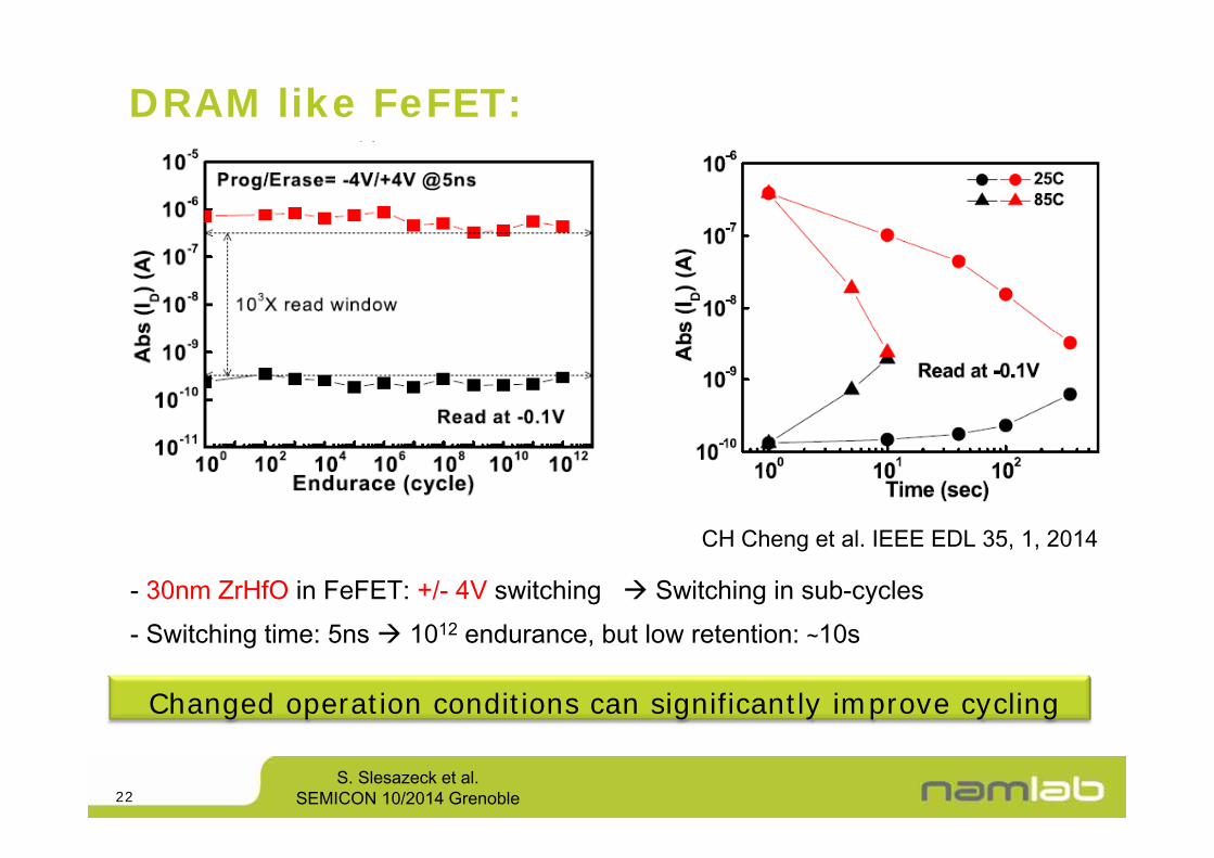
Summary
Material:
A ferroelectric phase in HfO2 thin films can be stabilizedp 2
Ferroelectric phase most likely orthorhombic phase
Several stabilizing dopants have been identified
Ferroelectric Devices:
1T/1C: FE-HfO2 adds the 3rd dimension to FRAM scaling1T/1C: FE HfO2 adds the 3rd dimension to FRAM scaling
World‘s first 28nm FeFET device
HfO2-based FeFET added to ITRS roadmap in 2014:
Most promising ‚Emerging Memory‘ concept
FeFET meets already some DRAM and FLASH specification
Superior control of dopant concentration in ALD nanolaminates
and usbsequent crystallization of the film is mandatory
28S. Slesazeck et al.
SEMICON 10/2014 Grenoble
Thank you for your attention
This work was supported in part by the EFRE fund of the European Commission within the scope of technology development and in part by the Free State of Saxony
(Project: Cool Memory, Heiko, Merlin)
and by funding of the Deutsche Forschungs Gemeinschaft(DFG) (Project: Inferox)
29S. Slesazeck et al.
SEMICON 10/2014 Grenoble
( j )
Thanks to the FeFET – TEAM:
2 3 4
5 6 7 8 9
dand many more:
U. Schröder1, E. Yurchuk1, J. Mueller2, S. Mueller1, T. Mikolajick1
T. Boescke4, D. Martin1, D. Zhou1, J. Sundqvist2, P. Polakowski2, T. Schenk1, U. Boettger5, D. Braeuhaus5, S. Starschich5, C. Adelmann6, M.
Popovici6, T. Schloesser3, M. Trentzsch3 , M. Goldbach3, R.v. Bentum3, S. p , , , , ,Knebel1, T. Olsen1, R. Hoffmann2, J. Paul2, R. Boschke3, A. Kumar7, T.M.
Arruda7, S.V. Kalinin7, M. Alexe8, A. Morelli8, A.Kersch9, R. Maverick9


![Sangeetha [Ferroelectric Memory]](https://static.documents.pub/doc/80x56/55cf8f91550346703b9d9665/sangeetha-ferroelectric-memory.jpg)


