614
Allwinner H3 Datasheet Quad-Core OTT Box Processor Version 1.2 Apr.23,2015 Copyright© 2015 Allwinner Technology Co.,Ltd. All Rights Reserved. confidential

Allwinner H3 Datasheet
Quad-Core OTT Box Processor
Version 1.2
Apr.23,2015
Copyright© 2015 Allwinner Technology Co.,Ltd. All Rights Reserved.
confid
ential

H3
H3 Datasheet(Revision1.2) Copyright© 2015 Allwinner Technology Co.,Ltd.All Rights Reserved. Page 2
Declaration
This documentation is the original work and copyrighted property of Allwinner Technology (“Allwinner”). Reproduction
in whole or in part must obtain the written approval of Allwinner and give clear acknowledgement to the copyright
owner.
The information furnished by Allwinner is believed to be accurate and reliable. Allwinner reserves the right to make
changes in circuit design and/or specifications at any time without notice. Allwinner does not assume any responsibility
and liability for its use. Nor for any infringements of patents or other rights of the third parties which may result from
its use. No license is granted by implication or otherwise under any patent or patent rights of Allwinner. This
documentation neither states nor implies warranty of any kind, including fitness for any particular application.
Third party licences may be required to implement the solution/product. Customers shall be solely responsible to
obtain all appropriately required third party licences. Allwinner shall not be liable for any licence fee or royalty due in
respect of any required third party licence. Allwinner shall have no warranty, indemnity or other obligations with
respect to matters covered under any required third party licence.
confid
ential
H3
H3 Datasheet(Revision1.2) Copyright© 2015 Allwinner Technology Co.,Ltd.All Rights Reserved. Page 3
Revision History
Version Date Description
V1.0 Nov.18,2014 Initial release version
V1.1 Jan.26,2015 Correct PWM Description
V1.2 Apr.23,2015 Add the programming guide of crypto engine
confid
ential
H3
H3 Datasheet(Revision1.2) Copyright© 2015 Allwinner Technology Co.,Ltd.All Rights Reserved. Page 4
Table of Contents
Declaration ............................................................................................................................................................................ 2
Revision History..................................................................................................................................................................... 3
Table of Contents .................................................................................................................................................................. 4
Chapter 1 About This Documentation ......................................................................................................................... 51
1.1. Documentation Overview ........................................................................................................................... 51
1.2. Acronyms and abbreviations ....................................................................................................................... 51
Chapter 2 Overview ..................................................................................................................................................... 55
2.1. Processor Features ...................................................................................................................................... 56
2.1.1. CPU Architecture ................................................................................................................................. 56
2.1.2. GPU Architecture ................................................................................................................................. 56
2.1.3. Memory Subsystem ............................................................................................................................. 56
2.1.3.1. Boot ROM .................................................................................................................................... 56
2.1.3.2. SDRAM ........................................................................................................................................ 56
2.1.3.3. NAND Flash ................................................................................................................................. 57
2.1.3.4. SD/MMC ...................................................................................................................................... 57
2.1.4. System Peripheral ................................................................................................................................ 57
2.1.4.1. Timer ........................................................................................................................................... 57
2.1.4.2. High Speed Timer ........................................................................................................................ 58
2.1.4.3. RTC .............................................................................................................................................. 58
2.1.4.4. GIC ............................................................................................................................................... 58
2.1.4.5. DMA ............................................................................................................................................ 58
confid
ential

H3
H3 Datasheet(Revision1.2) Copyright© 2015 Allwinner Technology Co.,Ltd.All Rights Reserved. Page 5
2.1.4.6. CCU .............................................................................................................................................. 58
2.1.4.7. PWM ........................................................................................................................................... 58
2.1.4.8. Crypto Engine(CE) ....................................................................................................................... 59
2.1.4.9. Security ID ................................................................................................................................... 59
2.1.4.10. CPU Configuration ..................................................................................................................... 59
2.1.4.11. Power Management ................................................................................................................. 59
2.1.5. Display Subsystem ............................................................................................................................... 59
2.1.5.1. DE2.0 ........................................................................................................................................... 59
2.1.5.2. Display Output ............................................................................................................................ 60
2.1.6. Video Engine ....................................................................................................................................... 60
2.1.6.1. Video Decoding ........................................................................................................................... 60
2.1.6.2. Video Encoding ........................................................................................................................... 60
2.1.7. Image Subsystem ................................................................................................................................. 61
2.1.7.1. CSI................................................................................................................................................ 61
2.1.8. Audio Subsystem ................................................................................................................................. 61
2.1.8.1. Audio Codec ................................................................................................................................ 61
2.1.8.2. One Wire Audio(OWA) ................................................................................................................ 61
2.1.8.3. I2S/PCM....................................................................................................................................... 61
2.1.9. External Peripherals ............................................................................................................................ 62
2.1.9.1. USB .............................................................................................................................................. 62
2.1.9.2. Ethernet ...................................................................................................................................... 62
2.1.9.3. ADC .............................................................................................................................................. 62
2.1.9.4. CIR ............................................................................................................................................... 63
2.1.9.5. UART............................................................................................................................................ 63
confid
ential
H3
H3 Datasheet(Revision1.2) Copyright© 2015 Allwinner Technology Co.,Ltd.All Rights Reserved. Page 6
2.1.9.6. SPI ................................................................................................................................................ 63
2.1.9.7. TWI .............................................................................................................................................. 63
2.1.9.8. TS ................................................................................................................................................. 63
2.1.9.9. SCR .............................................................................................................................................. 64
2.1.10. Package ................................................................................................................................................ 64
2.2. System Block Diagram ................................................................................................................................. 65
Chapter 3 Pin Description ............................................................................................................................................ 66
3.1. Pin Characteristics ....................................................................................................................................... 66
3.2. GPIO Multiplexing Functions ....................................................................................................................... 74
3.3. Detailed Pin/Signal Description ................................................................................................................... 78
Chapter 4 System ......................................................................................................................................................... 83
4.1. Memory Mapping ....................................................................................................................................... 84
4.2. Boot System ................................................................................................................................................ 86
4.3. CCU .............................................................................................................................................................. 87
4.3.1. Overview ............................................................................................................................................. 87
4.3.2. Functionalities Description .................................................................................................................. 87
4.3.2.1. System Bus .................................................................................................................................. 87
4.3.2.2. Bus clock tree .............................................................................................................................. 89
4.3.3. Typical Applications ............................................................................................................................. 89
4.3.4. Register List ......................................................................................................................................... 90
4.3.5. Register Description ............................................................................................................................ 92
4.3.5.1. PLL_CPUX Control Register (Default Value: 0x00001000) .......................................................... 92
4.3.5.2. PLL_Audio Control Register (Default Value: 0x00035514) .......................................................... 93
4.3.5.3. PLL_VIDEO Control Register (Default Value: 0x03006207).......................................................... 94
confid
ential

H3
H3 Datasheet(Revision1.2) Copyright© 2015 Allwinner Technology Co.,Ltd.All Rights Reserved. Page 7
4.3.5.4. PLL_VE Control Register (Default Value: 0x03006207)................................................................ 95
4.3.5.5. PLL_DDR Control Register (Default Value: 0x00001000) ............................................................. 96
4.3.5.6. PLL_PERIPH0 Control Register (Default Value: 0x00041811) ...................................................... 97
4.3.5.7. PLL_GPU Control Register (Default Value: 0x03006207) ............................................................. 98
4.3.5.8. PLL_PERIPH1 Control Register (Default Value: 0x00041811) ...................................................... 99
4.3.5.9. PLL_DE Control Register (Default Value: 0x03006207) ............................................................. 100
4.3.5.10. CPUX/AXI Configuration Register (Default Value: 0x00010000) ............................................. 101
4.3.5.11. AHB1/APB1 Configuration Register (Default Value: 0x00001010)........................................... 102
4.3.5.12. APB2 Configuration Register (Default Value: 0x01000000) .................................................... 102
4.3.5.13. AHB2 Configuration Register (Default Value: 0x00000000) .................................................... 103
4.3.5.14. Bus Clock Gating Register0 (Default Value: 0x00000000) ....................................................... 103
4.3.5.15. Bus Clock Gating Register1 (Default Value: 0x00000000) ....................................................... 105
4.3.5.16. Bus Clock Gating Register2 (Default Value: 0x00000000) ....................................................... 106
4.3.5.17. Bus Clock Gating Register3 (Default Value: 0x00000000) ....................................................... 107
4.3.5.18. Bus Clock Gating Register4 (Default Value: 0x00000000) ....................................................... 108
4.3.5.19. THS Clock Register (Default Value: 0x00000000) .................................................................... 109
4.3.5.20. NAND Clock Register (Default Value: 0x00000000) ................................................................ 109
4.3.5.21. SDMMC0 Clock Register (Default Value: 0x00000000) ........................................................... 110
4.3.5.22. SDMMC1 Clock Register (Default Value: 0x00000000) ........................................................... 111
4.3.5.23. SDMMC2 Clock Register (Default Value: 0x00000000) ........................................................... 112
4.3.5.24. TS Clock Register (Default Value: 0x00000000) ....................................................................... 113
4.3.5.25. CE Clock Register (Default Value: 0x00000000) ...................................................................... 113
4.3.5.26. SPI0 Clock Register (Default Value: 0x00000000) ................................................................... 114
4.3.5.27. SPI1 Clock Register (Default Value: 0x00000000) ................................................................... 114
confid
ential

H3
H3 Datasheet(Revision1.2) Copyright© 2015 Allwinner Technology Co.,Ltd.All Rights Reserved. Page 8
4.3.5.28. I2S/PCM 0 Clock Register (Default Value: 0x00000000) ......................................................... 115
4.3.5.29. I2S/PCM 1 Clock Register (Default Value: 0x00000000) ......................................................... 116
4.3.5.30. I2S/PCM 2 Clock Register (Default Value: 0x00000000) ......................................................... 116
4.3.5.31. OWA Clock Register (Default Value: 0x00000000) .................................................................. 116
4.3.5.32. USBPHY Configuration Register (Default Value: 0x00000000) ................................................ 117
4.3.5.33. DRAM Configuration Register (Default Value: 0x00000000) ................................................... 118
4.3.5.34. MBUS Reset Register (Default Value: 0x80000000) ................................................................ 119
4.3.5.35. DRAM Clock Gating Register (Default Value: 0x00000000)..................................................... 119
4.3.5.36. DE Clock Gating Register (Default Value: 0x00000000) .......................................................... 119
4.3.5.37. TCON0 Clock Register (Default Value: 0x00000000) ............................................................... 120
4.3.5.38. TVE Clock Register (Default Value: 0x00000000) .................................................................... 120
4.3.5.39. DEINTERLACE Clock Register (Default Value: 0x00000000) .................................................... 121
4.3.5.40. CSI_MISC Clock Register (Default Value: 0x00000000) ........................................................... 121
4.3.5.41. CSI Clock Register (Default Value: 0x00000000) ..................................................................... 121
4.3.5.42. VE Clock Register (Default Value: 0x00000000) ...................................................................... 122
4.3.5.43. AC Digital Clock Register (Default Value: 0x00000000) ........................................................... 123
4.3.5.44. AVS Clock Register (Default Value: 0x00000000) .................................................................... 123
4.3.5.45. HDMI Clock Register (Default Value: 0x00000000) ................................................................. 123
4.3.5.46. HDMI Slow Clock Register (Default Value: 0x00000000) ........................................................ 124
4.3.5.47. MBUS Clock Register (Default Value: 0x00000000) ................................................................ 124
4.3.5.48. GPU Clock Register (Default Value: 0x00000000) ................................................................... 124
4.3.5.49. PLL Stable Time Register0 (Default Value: 0x000000FF) ......................................................... 125
4.3.5.50. PLL Stable Time Register1 (Default Value: 0x000000FF) ......................................................... 125
4.3.5.51. PLL_CPUX Bias Register (Default Value: 0x08100200) ............................................................ 125
confid
ential
H3
H3 Datasheet(Revision1.2) Copyright© 2015 Allwinner Technology Co.,Ltd.All Rights Reserved. Page 9
4.3.5.52. PLL_AUDIO Bias Register (Default Value: 0x10100000) .......................................................... 126
4.3.5.53. PLL_VIDEO Bias Register (Default Value: 0x10100000) ........................................................... 126
4.3.5.54. PLL_VE Bias Register (Default Value: 0x10100000) ................................................................. 126
4.3.5.55. PLL_DDR Bias Register (Default Value: 0x81104000) .............................................................. 127
4.3.5.56. PLL_PERIPH0 Bias Register (Default Value: 0x10100010) ....................................................... 127
4.3.5.57. PLL_GPU Bias Register (Default Value: 0x10100000) .............................................................. 128
4.3.5.58. PLL_PERIPH1 Bias Register (Default Value: 0x10100010) ....................................................... 128
4.3.5.59. PLL_DE Bias Register (Default Value: 0x10100000) ................................................................. 129
4.3.5.60. PLL_CPUX Tuning Register (Default Value: 0x0A101000) ........................................................ 129
4.3.5.61. PLL_DDR Tuning Register (Default Value: 0x14880000) .......................................................... 130
4.3.5.62. PLL_CPUX Pattern Control Register (Default Value: 0x00000000) .......................................... 130
4.3.5.63. PLL_AUDIO Pattern Control Register(Default Value: 0x00000000) ......................................... 131
4.3.5.64. PLL_VIDEO Pattern Control Register (Default Value: 0x00000000) ......................................... 131
4.3.5.65. PLL_VE Pattern Control Register (Default Value: 0x00000000) ............................................... 132
4.3.5.66. PLL_DDR Pattern Control Register (Default Value: 0x00000000) ............................................ 132
4.3.5.67. PLL_GPU Pattern Control Register (Default Value: 0x00000000) ............................................ 133
4.3.5.68. PLL_PERIPH1 Pattern Control Register (Default Value: 0x00000000) ..................................... 133
4.3.5.69. PLL_DE Pattern Control Register (Default Value: 0x00000000) .............................................. 134
4.3.5.70. Bus Software Reset Register 0 (Default Value: 0x00000000) .................................................. 134
4.3.5.71. Bus Software Reset Register 1 (Default Value: 0x00000000) .................................................. 137
4.3.5.72. Bus Software Reset Register 2 (Default Value: 0x00000000) .................................................. 138
4.3.5.73. Bus Software Reset Register 3 (Default Value: 0x00000000) .................................................. 138
4.3.5.74. Bus Software Reset Register 4 (Default Value: 0x00000000) .................................................. 139
4.3.5.75. CCU Security Switch Register (Default Value: 0x00000000) .................................................... 140
confid
ential
H3
H3 Datasheet(Revision1.2) Copyright© 2015 Allwinner Technology Co.,Ltd.All Rights Reserved. Page 10
4.3.5.76. PS Control Register (Default Value: 0x00000000) ................................................................... 140
4.3.5.77. PS Counter Register (Default Value: 0x00000000) .................................................................. 141
4.3.6. Programming Guidelines ................................................................................................................... 142
4.3.6.1. PLL ............................................................................................................................................. 142
4.3.6.2. BUS ............................................................................................................................................ 142
4.3.6.3. Clock Switch .............................................................................................................................. 142
4.3.6.4. Gating and reset ........................................................................................................................ 142
4.4. CPU Configuration ..................................................................................................................................... 143
4.4.1. Overview ........................................................................................................................................... 143
4.4.2. Register List ....................................................................................................................................... 143
4.4.3. Register Description .......................................................................................................................... 144
4.4.3.1. CPUS Reset Control Register(Default Value: 0x00000000) ........................................................ 144
4.4.3.2. CPU0 Reset Control Register(Default Value: 0x00000000) ....................................................... 144
4.4.3.3. CPU0 Control Register(Default Value: 0x00000000) ................................................................. 144
4.4.3.4. CPU0 Status Register (Default Value: 0x00000000) .................................................................. 145
4.4.3.5. CPU1 Reset Register(Default Value: 0x00000001) .................................................................... 145
4.4.3.6. CPU1 Control Register(Default Value: 0x00000000) ................................................................. 145
4.4.3.7. CPU1 Status Register(Default Value: 0x00000000) ................................................................... 146
4.4.3.8. CPU2 Reset Control Register(Default Value: 0x00000001) ....................................................... 146
4.4.3.9. CPU2 Control Register(Default Value: 0x00000000) ................................................................. 147
4.4.3.10. CPU2 Status Register(Default Value: 0x00000000) ................................................................. 147
4.4.3.11. CPU3 Reset Control Register(Default Value: 0x00000001) ..................................................... 147
4.4.3.12. CPU3 Control Register(Default Value: 0x00000000) ............................................................... 148
4.4.3.13. CPU3 Status Register(Default Value: 0x00000000) ................................................................. 148
confid
ential
H3
H3 Datasheet(Revision1.2) Copyright© 2015 Allwinner Technology Co.,Ltd.All Rights Reserved. Page 11
4.4.3.14. CPU System Reset Control Register(Default Value: 0x00000001) ........................................... 148
4.4.3.15. CPU Clock Gating Register(Default Value: 0x0000010F) ......................................................... 149
4.4.3.16. General Control Register(Default Value: 0x00000020) ........................................................... 149
4.4.3.17. Super Standby Flag Register(Default Value: 0x00000000) ...................................................... 149
4.4.3.18. 64-bit Counter Control Register(Default Value: 0x00000000) ................................................ 150
4.4.3.19. 64-bit Counter Low Register(Default Value: 0x00000000) ...................................................... 150
4.4.3.20. 64-bit Counter High Register(Default Value: 0x00000000) ..................................................... 151
4.5. System Control .......................................................................................................................................... 152
4.5.1. Overview ........................................................................................................................................... 152
4.5.2. System Control Register List .............................................................................................................. 152
4.5.3. System Control Register Description ................................................................................................. 152
4.5.3.1. Version Register ......................................................................................................................... 152
4.5.3.2. EMAC Clock Register (Default Value: 0x00058000) ................................................................... 153
4.6. Timer ......................................................................................................................................................... 155
4.6.1. Overview ........................................................................................................................................... 155
4.6.2. Block Diagram ................................................................................................................................... 155
4.6.3. Timer Register List ............................................................................................................................. 156
4.6.4. Timer Register Description ................................................................................................................ 156
4.6.4.1. Timer IRQ Enable Register (Default Value: 0x00000000) .......................................................... 156
4.6.4.2. Timer IRQ Status Register (Default Value: 0x00000000) ........................................................... 157
4.6.4.3. Timer 0 Control Register (Default Value: 0x00000004) ............................................................. 157
4.6.4.4. Timer 0 Interval Value Register ................................................................................................. 158
4.6.4.5. Timer 0 Current Value Register ................................................................................................. 158
4.6.4.6. Timer 1 Control Register (Default Value: 0x00000004) ............................................................. 158
confid
ential

H3
H3 Datasheet(Revision1.2) Copyright© 2015 Allwinner Technology Co.,Ltd.All Rights Reserved. Page 12
4.6.4.7. Timer 1 Interval Value Register ................................................................................................. 159
4.6.4.8. Timer 1 Current Value Register ................................................................................................. 160
4.6.4.9. AVS Counter Control Register (Default Value: 0x00000000) ..................................................... 160
4.6.4.10. AVS Counter 0 Register (Default Value: 0x00000000) ............................................................. 160
4.6.4.11. AVS Counter 1 Register (Default Value: 0x00000000) ............................................................. 161
4.6.4.12. AVS Counter Divisor Register (Default Value: 0x05DB05DB)................................................... 161
4.6.4.13. Watchdog0 IRQ Enable Register (Default Value: 0x00000000) ............................................... 162
4.6.4.14. Watchdog0 Status Register (Default Value: 0x00000000) ....................................................... 162
4.6.4.15. Watchdog0 Control Register (Default Value: 0x00000000) ..................................................... 162
4.6.4.16. Watchdog0 Configuration Register (Default Value: 0x00000001) ........................................... 163
4.6.4.17. Watchdog0 Mode Register (Default Value: 0x00000000) ....................................................... 163
4.6.5. Programming Guidelines ................................................................................................................... 164
4.6.5.1. Timer ......................................................................................................................................... 164
4.6.5.2. Watchdog Reset ......................................................................................................................... 164
4.6.5.3. Watchdog Restart ...................................................................................................................... 164
4.7. Trusted Watchdog ..................................................................................................................................... 165
4.7.1. Overview ........................................................................................................................................... 165
4.7.2. Block Diagram ................................................................................................................................... 165
4.7.3. Functionalities Description ................................................................................................................ 165
4.7.3.1. TWD Reset ................................................................................................................................. 165
4.7.3.2. NV-Counter ................................................................................................................................ 166
4.7.4. TWD Register List .............................................................................................................................. 166
4.7.5. TWD Register Description ................................................................................................................. 167
4.7.5.1. TWD Status Register (Default Value: 0x00000000) ................................................................... 167
confid
ential

H3
H3 Datasheet(Revision1.2) Copyright© 2015 Allwinner Technology Co.,Ltd.All Rights Reserved. Page 13
4.7.5.2. TWD Control Register (Default Value: 0x00000000) ................................................................. 167
4.7.5.3. TWD Restart Register (Default Value: 0x00000000) .................................................................. 168
4.7.5.4. TWD Low Counter Register (Default Value: 0x00000000) ......................................................... 168
4.7.5.5. TWD High Counter Register (Default Value: 0x00000000) ........................................................ 168
4.7.5.6. TWD Interval Value Register (Default Value: 0x00000000) ....................................................... 168
4.7.5.7. TWD Low Counter Compare Register (Default Value: 0x00000000) ......................................... 168
4.7.5.8. TWD High Counter Compare Register (Default Value: 0x00000000) ........................................ 169
4.7.5.9. Secure Storage NV-Counter Register (Default Value: 0x00000000) .......................................... 169
4.7.5.10. Synchronize Data Counter Register 0 (Default Value: 0x00000000) ....................................... 169
4.7.5.11. Synchronize Data Counter Register 1 (Default Value: 0x00000000) ....................................... 169
4.7.5.12. Synchronize Data Counter Register 2 (Default Value: 0x00000000) ....................................... 169
4.7.5.13. Synchronize Data Counter Register 3 (Default Value: 0x00000000) ....................................... 170
4.8. RTC ............................................................................................................................................................ 171
4.8.1. Overview ........................................................................................................................................... 171
4.8.2. RTC Register List ................................................................................................................................ 171
4.8.3. RTC Register Description ................................................................................................................... 172
4.8.3.1. LOSC Control Register (Default Value: 0x00004000) ................................................................. 172
4.8.3.2. LOSC Auto Switch Status Register (Default Value: 0x00000000) ............................................... 173
4.8.3.3. Internal OSC Clock Prescalar Register (Default Value: 0x0000000F) ......................................... 173
4.8.3.4. RTC YY-MM-DD Register (Default Value: 0x00000000) ............................................................. 173
4.8.3.5. RTC HH-MM-SS Register (Default Value: 0x00000000) ............................................................. 174
4.8.3.6. Alarm 0 Counter Register (Default Value: 0x00000000) ........................................................... 175
4.8.3.7. Alarm 0 Current Value Register ................................................................................................. 175
4.8.3.8. Alarm 0 Enable Register (Default Value: 0x00000000) ............................................................. 175
confid
ential
H3
H3 Datasheet(Revision1.2) Copyright© 2015 Allwinner Technology Co.,Ltd.All Rights Reserved. Page 14
4.8.3.9. Alarm 0 IRQ Enable Register (Default Value: 0x00000000) ....................................................... 175
4.8.3.10. Alarm 0 IRQ Status Register (Default Value: 0x00000000) ...................................................... 176
4.8.3.11. Alarm 1 Week HH-MM-SS Register (Default Value: 0x00000000) .......................................... 176
4.8.3.12. Alarm 1 Enable Register (Default Value: 0x00000000) ........................................................... 176
4.8.3.13. Alarm 1 IRQ Enable Register (Default Value: 0x00000000) ..................................................... 178
4.8.3.14. Alarm 1 IRQ Status Register (Default Value: 0x00000000) ...................................................... 178
4.8.3.15. Alarm Config Register (Default Value: 0x00000000) ............................................................... 178
4.8.3.16. LOSC Output Gating Register (Default Value: 0x00000000) .................................................... 178
4.8.3.17. General Purpose Register (Default Value: 0x00000000)) ........................................................ 179
4.8.3.18. RTC Debug Register (Default Value: 0x00000000) .................................................................. 179
4.8.3.19. GPL Hold Output Register (Default Value: 0x00000000) ......................................................... 179
4.8.3.20. VDD RTC Regulation Register (Default Value: 0x00000004) .................................................... 181
4.8.3.21. IC Characteristic Register (Default Value: 0x00000000) .......................................................... 181
4.9. High-speed Timer ...................................................................................................................................... 183
4.9.1. Overview ........................................................................................................................................... 183
4.9.2. Operation Principle ........................................................................................................................... 183
4.9.2.1. HSTimer clock gating and software reset .................................................................................. 183
4.9.2.2. HSTimer reload bit .................................................................................................................... 183
4.9.3. HSTimer Register List ........................................................................................................................ 183
4.9.4. HSTimer Register Description ........................................................................................................... 184
4.9.4.1. HS Timer IRQ Enable Register (Default Value: 0x00000000) .................................................... 184
4.9.4.2. HS Timer IRQ Status Register (Default Value: 0x00000000) ..................................................... 184
4.9.4.3. HS Timer Control Register (Default Value: 0x00000000) .......................................................... 184
4.9.4.4. HS Timer Interval Value Lo Register .......................................................................................... 185
confid
ential

H3
H3 Datasheet(Revision1.2) Copyright© 2015 Allwinner Technology Co.,Ltd.All Rights Reserved. Page 15
4.9.4.5. HS Timer Interval Value Hi Register .......................................................................................... 185
4.9.4.6. HS Timer Current Value Lo Register .......................................................................................... 186
4.9.4.7. HS Timer Current Value Hi Register .......................................................................................... 186
4.9.5. Programming Guidelines ................................................................................................................... 186
4.10. PWM.......................................................................................................................................................... 187
4.10.1. Overview ........................................................................................................................................... 187
4.10.2. PWM Block Diagram .......................................................................................................................... 187
4.10.3. PWM Register List ............................................................................................................................. 187
4.10.4. PWM Register Description ................................................................................................................ 188
4.10.4.1. PWM Control Register(Default Value: 0x00000000) ............................................................... 188
4.10.4.2. PWM Channel 0 Period Register(Default Value: 0x00000000) ............................................... 189
4.11. DMA .......................................................................................................................................................... 190
4.11.1. Overview ........................................................................................................................................... 190
4.11.2. Functionalities Description ................................................................................................................ 190
4.11.2.1. Block Diagram ......................................................................................................................... 190
4.11.2.2. DRQ Type and Corresponding Relation ................................................................................... 191
4.11.2.3. DMA Descriptor ....................................................................................................................... 191
4.11.3. DMA Register List .............................................................................................................................. 192
4.11.4. DMA Register Description ................................................................................................................. 193
4.11.4.1. DMA IRQ Enable Register0 (Default Value: 0x00000000) ....................................................... 193
4.11.4.2. DMA IRQ Enable Register1 (Default Value: 0x00000000) ....................................................... 195
4.11.4.3. DMA IRQ Pending Status Register0 (Default Value: 0x00000000) .......................................... 196
4.11.4.4. DMA IRQ Pending Status Register1 (Default Value: 0x00000000) .......................................... 198
4.11.4.5. DMA Security Register (Default Value: 0x00000000) .............................................................. 199
confid
ential
H3
H3 Datasheet(Revision1.2) Copyright© 2015 Allwinner Technology Co.,Ltd.All Rights Reserved. Page 16
4.11.4.6. DMA Auto Gating Register (Default Value: 0x00000000)........................................................ 201
4.11.4.7. DMA Status Register (Default Value: 0x00000000) ................................................................. 201
4.11.4.8. DMA Channel Enable Register (Default Value: 0x00000000) .................................................. 202
4.11.4.9. DMA Channel Pause Register (Default Value: 0x00000000) ................................................... 203
4.11.4.10. DMA Channel Descriptor Address Register (Default Value: 0x00000000) ............................ 203
4.11.4.11. DMA Channel Configuration Register (Default Value: 0x00000000) ..................................... 203
4.11.4.12. DMA Channel Current Source Address Register (Default Value: 0x00000000) ..................... 204
4.11.4.13. DMA Channel Current Destination Address Register (Default Value: 0x00000000) ............. 204
4.11.4.14. DMA Channel Byte Counter Left Register (Default Value: 0x00000000) .............................. 204
4.11.4.15. DMA Channel Parameter Register (Default Value: 0x00000000) .......................................... 205
4.11.4.16. DMA Former Descriptor Address Register (Default Value: 0x00000000) .............................. 205
4.11.4.17. DMA Package Number Register (Default Value: 0x00000000).............................................. 205
4.12. GIC ............................................................................................................................................................. 206
4.12.1. Interrupt Source ................................................................................................................................ 206
4.13. Message Box .............................................................................................................................................. 210
4.13.1. Overview ........................................................................................................................................... 210
4.13.2. Functionalities Description ................................................................................................................ 210
4.13.2.1. Typical Applications ................................................................................................................. 211
4.13.2.2. Functional Block Diagram ........................................................................................................ 212
4.13.3. Operation Principle ........................................................................................................................... 212
4.13.3.1. Message Queue Assignment ................................................................................................... 212
4.13.3.2. Interrupt request ..................................................................................................................... 213
4.13.4. Message Box Register List ................................................................................................................. 213
4.13.5. Message Box Register Description .................................................................................................... 214
confid
ential

H3
H3 Datasheet(Revision1.2) Copyright© 2015 Allwinner Technology Co.,Ltd.All Rights Reserved. Page 17
4.13.5.1. MSGBox Control Register 0(Default Value: 0x10101010) ....................................................... 214
4.13.5.2. MSGBox Control Register 1(Default Value: 0x10101010) ....................................................... 215
4.13.5.3. MSGBox IRQ Enable Register (Default Value: 0x00000000) .................................................... 216
4.13.5.4. MSGBox IRQ Status Register u(Default Value: 0x0000AAAA) .................................................. 217
4.13.5.5. MSGBox FIFO Status Register m(Default Value: 0x00000000) ................................................ 219
4.13.5.6. MSGBox Message Status Register m(Default Value: 0x00000000) ......................................... 219
4.13.5.7. MSGBox Message Queue Register (Default Value: 0x00000000) ........................................... 219
4.14. Spinlock ..................................................................................................................................................... 221
4.14.1. Overview ........................................................................................................................................... 221
4.14.2. Functionalities Description ................................................................................................................ 222
4.14.2.1. Typical Applications ................................................................................................................. 222
4.14.2.2. Functional Block Diagram ........................................................................................................ 222
4.14.3. Operation Principle ........................................................................................................................... 223
4.14.3.1. Spinlock clock gating and software reset ................................................................................ 223
4.14.3.2. Take and free a spinlock .......................................................................................................... 223
4.14.4. Spinlock Register List ......................................................................................................................... 223
4.14.5. Spinlock Register Description ............................................................................................................ 223
4.14.5.1. Spinlock System Status Register (Default Value: 0x10000000) ............................................... 223
4.14.5.2. Spinlock Register Status (Default Value: 0x00000000) ............................................................ 224
4.14.5.3. Spinlock Register N (N=0 to 31)(Default Value: 0x00000000) ................................................. 224
4.14.6. Programming Guidelines ................................................................................................................... 225
4.15. Crypto Engine ............................................................................................................................................ 226
4.15.1. Overview ........................................................................................................................................... 226
4.15.2. Functionalities Description ................................................................................................................ 226
confid
ential

H3
H3 Datasheet(Revision1.2) Copyright© 2015 Allwinner Technology Co.,Ltd.All Rights Reserved. Page 18
4.15.2.1. Block Diagram ......................................................................................................................... 227
4.15.2.2. Crypto Engine Task Descriptor................................................................................................. 227
4.15.3. Crypto Engine Register List ................................................................................................................ 230
4.15.4. Crypto Engine Register Description ................................................................................................... 230
4.15.4.1. Crypto Engine Task Descriptor Queue Register(Default Value: 0x00000000) ......................... 230
4.15.4.2. Crypto Engine Control Register ............................................................................................... 231
4.15.4.3. Crypto Engine Interrupt Control Register(Default Value: 0x00000000).................................. 231
4.15.4.4. Crypto Engine Interrupt Status Register(Default Value: 0x00000000).................................... 231
4.15.4.5. Crypto Engine Task Load Register(Default Value: 0x00000000) ............................................. 231
4.15.4.6. Crypto Engine Error Status Register(Default Value: 0x00000000) .......................................... 232
4.15.4.7. Crypto Engine Current Source Scatter Group Register(Default Value: 0x00000000) .............. 232
4.15.4.8. Crypto Engine Current Destination Scatter Group Register(Default Value: 0x00000000) ...... 232
4.15.4.9. Crypto Engine Current Source Address Register(Default Value: 0x00000000) ....................... 233
4.15.4.10. Crypto Engine Current Destination Address Register(Default Value: 0x00000000).............. 233
4.15.4.11. Crypto Engine Throughput Register(Default Value: 0x00000000) ........................................ 233
4.15.5. Crypto Engine Clock Requirement ..................................................................................................... 233
4.15.6. Programming Guidelines ................................................................................................................... 233
4.16. Security ID ................................................................................................................................................. 236
4.16.1. Overview ........................................................................................................................................... 236
4.17. Secure Memory Controller ........................................................................................................................ 237
4.17.1. Overview ........................................................................................................................................... 237
4.17.2. Functionalities Description ................................................................................................................ 237
4.17.2.1. DRM Block Diagram ................................................................................................................ 238
4.17.2.2. Master ID Table ....................................................................................................................... 238
confid
ential

H3
H3 Datasheet(Revision1.2) Copyright© 2015 Allwinner Technology Co.,Ltd.All Rights Reserved. Page 19
4.17.2.3. Region Size Table ..................................................................................................................... 239
4.17.2.4. Security inversion is disabled .................................................................................................. 239
4.17.2.5. Security inversion is enabled ................................................................................................... 240
4.17.3. SMC Register List ............................................................................................................................... 240
4.17.4. SMC Register Description .................................................................................................................. 241
4.17.4.1. SMC Configuration Register(Default Value: 0x00001F0F)....................................................... 241
4.17.4.2. SMC Action Register(Default Value: 0x00000001) .................................................................. 241
4.17.4.3. SMC Lockdown Range Register(Default Value: 0x00000000) ................................................. 242
4.17.4.4. SMC Lockdown Select Register(Default Value: 0x00000000) ................................................. 242
4.17.4.5. SMC Interrupt Status Register(Default Value: 0x00000000) ................................................... 243
4.17.4.6. SMC Interrupt Clear Register(Default Value: 0x00000000) .................................................... 243
4.17.4.7. SMC Master Bypass Register(Default Value: 0xFFFFFFFF) ...................................................... 243
4.17.4.8. SMC Master Secure Register(Default Value: 0x00000000) ..................................................... 243
4.17.4.9. SMC Fail Address Register(Default Value: 0x00000000) ......................................................... 244
4.17.4.10. SMC Fail Control Register(Default Value: 0x00000000) ........................................................ 244
4.17.4.11. SMC Fail ID Register(Default Value: 0x00001F00) ................................................................ 245
4.17.4.12. SMC Speculation Control Register(Default Value: 0x00000000) .......................................... 245
4.17.4.13. SMC Security Inversion Enable Register(Default Value: 0x00000000) .................................. 245
4.17.4.14. SMC Master Attribute Register(Default Value: 0x00000000) ............................................... 246
4.17.4.15. DRM Master Enable Register(Default Value: 0x00000000) .................................................. 246
4.17.4.16. DRM Illegal Access Register(Default Value: 0x00000000) .................................................... 246
4.17.4.17. DRM Start Address Register(Default Value: 0x00000000) .................................................... 247
4.17.4.18. DRM End Address Register(Default Value: 0x00000000) ...................................................... 247
4.17.4.19. SMC Region Setup Low Register(Default Value: 0x00000000) ............................................. 247
confid
ential

H3
H3 Datasheet(Revision1.2) Copyright© 2015 Allwinner Technology Co.,Ltd.All Rights Reserved. Page 20
4.17.4.20. SMC Region Setup High Register(Default Value: 0x00000000)............................................. 247
4.17.4.21. SMC Region Attributes Register(Default Value: 0x00000000) .............................................. 248
4.18. Secure Memory Touch Arbiter .................................................................................................................. 249
4.18.1. Overview ........................................................................................................................................... 249
4.18.2. Functionalities Description ................................................................................................................ 249
4.18.2.1. Typical Applications ................................................................................................................. 249
4.18.2.2. SMTA Configuration Table ....................................................................................................... 249
4.18.3. SMTA Register List ............................................................................................................................. 250
4.18.4. SMTA Register Description ................................................................................................................ 250
4.18.4.1. SMTA DECPORT0 Status Register(Default Value: 0x00000000) .............................................. 250
4.18.4.2. SMTA DECPORT0 Set Register(Default Value: 0x00000000) ................................................... 250
4.18.4.3. SMTA DECPORT0 Clear Register(Default Value: 0x00000000) ................................................ 251
4.18.4.4. SMTA DECPORT1 Status Register(Default Value: 0x00000000) .............................................. 251
4.18.4.5. SMTA DECPORT1 Set Register(Default Value: 0x00000000) ................................................... 251
4.18.4.6. SMTA DECPORT1 Clear Register(Default Value: 0x00000000) ................................................ 252
4.18.4.7. SMTA DECPORT2 Status Register(Default Value: 0x00000000) .............................................. 252
4.18.4.8. SMTA DECPORT2 Set Register(Default Value: 0x00000000) ................................................... 252
4.18.4.9. SMTA DECPORT2 Clear Register(Default Value: 0x00000000) ................................................ 252
4.19. Thermal Sensor Controller ........................................................................................................................ 254
4.19.1. Overview ........................................................................................................................................... 254
4.19.2. Clock and Timing Requirements ....................................................................................................... 254
4.19.3. Thermal Sensor Register List ............................................................................................................. 254
4.19.4. Thermal Sensor Register Description ................................................................................................ 255
4.19.4.1. THS Control Register0 (Default Value: 0x00000000) ............................................................... 255
confid
ential
H3
H3 Datasheet(Revision1.2) Copyright© 2015 Allwinner Technology Co.,Ltd.All Rights Reserved. Page 21
4.19.4.2. THS Control Register1 (Default Value: 0x00000000) ............................................................... 255
4.19.4.3. ADC calibration Data Register (Default Value: 0x00000000) .................................................. 256
4.19.4.4. THS Control Register2 (Default Value: 0x00040000) ............................................................... 256
4.19.4.5. THS Interrupt Control Register (Default Value: 0x00000000).................................................. 256
4.19.4.6. THS status Register (Default Value: 0x00000000) ................................................................... 257
4.19.4.7. Alarm threshold Control Register (Default Value: 0x05a00684) ............................................. 258
4.19.4.8. Shutdown threshold Control Register (Default Value: 0x04e90000) ...................................... 258
4.19.4.9. Average filter Control Register (Default Value: 0x00000001) ................................................. 258
4.19.4.10. Thermal Sensor calibration Data Register (Default Value: 0x00000800) .............................. 258
4.19.4.11. THS Data Register (Default Value: 0x00000000) ................................................................... 259
4.19.5. Programming Guidelines ................................................................................................................... 259
4.20. KEY_ADC .................................................................................................................................................... 260
4.20.1. Overview ........................................................................................................................................... 260
4.20.2. Operation Principle ........................................................................................................................... 260
4.20.3. KEY_ADC Register List........................................................................................................................ 261
4.20.4. KEY_ADC Register Description........................................................................................................... 261
4.20.4.1. KEY_ADC Control Register (Default Value: 0x01000168) ........................................................ 261
4.20.4.2. KEY_ADC Interrupt Control Register (Default Value: 0x00000000) ......................................... 262
4.20.4.3. KEY_ADC Interrupt Status Register (Default Value: 0x00000000) ........................................... 263
4.20.4.4. KEY_ADC Data Register (Default Value: 0x00000000) ............................................................. 264
4.21. Audio Codec .............................................................................................................................................. 265
4.21.1. Overview ........................................................................................................................................... 265
4.21.2. Power and Signal Description ............................................................................................................ 265
4.21.2.1. Analog I/O Pins ........................................................................................................................ 265
confid
ential
H3
H3 Datasheet(Revision1.2) Copyright© 2015 Allwinner Technology Co.,Ltd.All Rights Reserved. Page 22
4.21.2.2. Filter/Reference ...................................................................................................................... 266
4.21.2.3. Power/Ground......................................................................................................................... 266
4.21.3. Data Path Diagram ............................................................................................................................ 266
4.21.4. Audio Codec Register List .................................................................................................................. 266
4.21.5. Audio Codec Register Description ..................................................................................................... 270
4.21.5.1. 0x00 DAC Digital Part Control Register(Default Value: 0x00000000) ...................................... 270
4.21.5.2. 0x04 DAC FIFO Control Register(Default Value: 0x00000F00) ................................................ 271
4.21.5.3. 0x08 DAC FIFO Status Register(Default Value: 0x00800088) .................................................. 273
4.21.5.4. 0x10 ADC FIFO Control Register(Default Value: 0x00000F00) ................................................ 273
4.21.5.5. 0x14 ADC FIFO Status Register(Default Value: 0x00000000) .................................................. 275
4.21.5.6. 0x18 ADC RX DATA Register(Default Value: 0x00000000) ....................................................... 276
4.21.5.7. 0x20 DAC TX DATA Register(Default Value: 0x00000000) ....................................................... 276
4.21.5.8. 0x40 DAC TX Counter Register(Default Value: 0x00000000) .................................................. 276
4.21.5.9. 0x44 ADC RX Counter Register(Default Value: 0x00000000) .................................................. 276
4.21.5.10. 0x48 DAC Debug Register(Default Value: 0x00000000) ........................................................ 277
4.21.5.11. 0x4C ADC Debug Register(Default Value: 0x00000000) ........................................................ 277
4.21.5.12. 0x60 DAC DAP Control Register(Default Value: 0x00000000) ............................................... 278
4.21.5.13. 0x70 ADC DAP Control Register(Default Value: 0x00000000) ............................................... 278
4.21.5.14. 0x74 ADC DAP Left Control Register(Default Value: 0x001F7000) ........................................ 279
4.21.5.15. 0x78 ADC DAP Right Control Register(Default Value: 0x001F7000) ...................................... 280
4.21.5.16. 0x7C ADC DAP Parameter Register(Default Value: 0x2C2C2828) ......................................... 282
4.21.5.17. 0x80 ADC DAP Left Average Coef Register(Default Value: 0x00051EB8) .............................. 282
4.21.5.18. 0x84 ADC DAP Left Decay & Attack Time Register(Default Value: 0x0000_001F) ................ 282
4.21.5.19. 0x88 ADC DAP Right Average Coef Register(Default Value: 0x00051EB8) ............................ 283
confid
ential
H3
H3 Datasheet(Revision1.2) Copyright© 2015 Allwinner Technology Co.,Ltd.All Rights Reserved. Page 23
4.21.5.20. 0x8C ADC DAP Right Decay & Attack Time Register(Default Value: 0x0000001F) ................ 283
4.21.5.21. 0x90 ADC DAP HPF Coef Register(Default Value: 0x00FF_FAC1) .......................................... 284
4.21.5.22. 0x94 ADC DAP Left Input Signal Low Average Coef Register(Default Value: 0x00051EB8) ... 284
4.21.5.23. 0x98 ADC DAP Right Input Signal Low Average Coef Register(Default Value: 0x00051EB8) . 284
4.21.5.24. 0x9C ADC DAP Optimum Register(Default Value: 0x00000000) ........................................... 284
4.21.5.25. 0x100 DAC DRC High HPF Coef Register(Default Value: 0x000000FF) .................................. 285
4.21.5.26. 0x104 DAC DRC Low HPF Coef Register(Default Value: 0x0000FAC1) .................................. 285
4.21.5.27. 0x108 DAC DRC Control Register(Default Value: 0x00000080) ............................................ 285
4.21.5.28. 0x10C DAC DRC Left Peak Filter High Attack Time Coef Register(Default Value: 0x0000_000B)
287
4.21.5.29. 0x110 DAC DRC Left Peak Filter Low Attack Time Coef Register(Default Value: 0x000077BF)
287
4.21.5.30. 0x114 DAC DRC Right Peak Filter High Attack Time Coef Register(Default Value: 0x0000000B)
287
4.21.5.31. 0x118 DAC DRC Peak Filter Low Attack Time Coef Register(Default Value: 0x000077BF) ... 287
4.21.5.32. 0x11C DAC DRC Left Peak Filter High Release Time Coef Register(Default Value: 0x000000FF)
288
4.21.5.33. 0x120 DAC DRC Left Peak Filter Low Release Time Coef Register(Default Value: 0x0000E1F8)
288
4.21.5.34. 0x124 DAC DRC Right Peak filter High Release Time Coef Register(Default Value:
0x0000_00FF) ............................................................................................................................................ 288
4.21.5.35. 0x128 DAC DRC Right Peak filter Low Release Time Coef Register(Default Value: 0x0000E1F8)
288
4.21.5.36. 0x12C DAC DRC Left RMS Filter High Coef Register(Default Value: 0x00000001) ................ 288
4.21.5.37. 0x130 DAC DRC Left RMS Filter Low Coef Register(Default Value: 0x00002BAF) ................ 289
4.21.5.38. 0x134 DAC DRC Right RMS Filter High Coef Register(Default Value: 0x00000001) .............. 289
4.21.5.39. 0x138 DAC DRC Right RMS Filter Low Coef Register(Default Value: 0x00002BAF) .............. 289
4.21.5.40. 0x13C DAC DRC Compressor Threshold High Setting Register(Default Value: 0x000006A4)
confid
ential

H3
H3 Datasheet(Revision1.2) Copyright© 2015 Allwinner Technology Co.,Ltd.All Rights Reserved. Page 24
289
4.21.5.41. 0x140 DAC DRC Compressor Threshold High Setting Register(Default Value: 0x0000_D3C0)
289
4.21.5.42. 0x144 DAC DRC Compressor Slope High Setting Register(Default Value: 0x00000080) ...... 290
4.21.5.43. 0x148 DAC DRC Compressor Slope Low Setting Register(Default Value: 0x0000_0000) ..... 290
4.21.5.44. 0x14C DAC DRC Compressor High Output at Compressor Threshold Register( Default Value:
0x0000F95B) ............................................................................................................................................. 290
4.21.5.45. 0x150 DAC DRC Compressor Low Output at Compressor Threshold Register(Default Value:
0x00002C3F).............................................................................................................................................. 290
4.21.5.46. 0x154 DAC DRC Limiter Theshold High Setting Register(Default Value: 0x000001A9) ........ 290
4.21.5.47. 0x158 DAC DRC Limiter Theshold Low Setting Register(Default Value: 0x0000_34F0) ........ 291
4.21.5.48. 0x15C DAC DRC Limiter Slope High Setting Register(Default Value: 0x0000_0005) ............ 291
4.21.5.49. 0x160 DAC DRC Limiter Slope Low Setting Register(Default Value: 0x00001EB8) ............... 291
4.21.5.50. 0x164 DAC DRC Limiter High Output at Limiter Threshold(Default Value: 0x0000FBD8) .... 291
4.21.5.51. 0x168 DAC DRC Limiter Low Output at Limiter Threshold(Default Value: 0x0000FBA7) ..... 291
4.21.5.52. 0x16C DAC DRC Expander Theshold High Setting Register(Default Value: 0x00000BA0) .... 292
4.21.5.53. 0x170 DAC DRC Expander Theshold Low Setting Register(Default Value: 0x00007291) ...... 292
4.21.5.54. 0x174 DAC DRC Expander Slope High Setting Register(Default Value: 0x00000500) ........... 292
4.21.5.55. 0x178 DAC DRC Expander Slope Low Setting Register(Default Value: 0x00000000)............ 292
4.21.5.56. 0x17C DAC DRC Expander High Output at Expander Threshold(Default Value: 0x0000F45F)
292
4.21.5.57. 0x180 DAC DRC Expander Low Output at Expander Threshold(Default Value: 0x00008D6E)
293
4.21.5.58. 0x184 DAC DRC Linear Slope High Setting Register(Default Value: 0x00000100) ................ 293
4.21.5.59. 0x188 DAC DRC Linear Slope Low Setting Register(Default Value: 0x00000000) ................. 293
4.21.5.60. 0x18C DAC DRC Smooth filter Gain High Attack Time Coef Register(Default Value:
0x00000002) ............................................................................................................................................. 293
confid
ential
H3
H3 Datasheet(Revision1.2) Copyright© 2015 Allwinner Technology Co.,Ltd.All Rights Reserved. Page 25
4.21.5.61. 0x190 DAC DRC Smooth filter Gain Low Attack Time Coef Register(Default Value:
0x00005600) ............................................................................................................................................. 293
4.21.5.62. 0x194 DAC DRC Smooth filter Gain High Release Time Coef Register(Default Value:
0x00000000) ............................................................................................................................................. 294
4.21.5.63. 0x198 DAC DRC Smooth filter Gain Low Release Time Coef Register(Default Value:
0x00000F04) .............................................................................................................................................. 294
4.21.5.64. 0x19C DAC DRC MAX Gain High Setting Register(Default Value: 0x0000FE56) .................... 294
4.21.5.65. 0x1A0 DAC DRC MAX Gain Low Setting Register(Default Value: 0x0000CB0F) .................... 294
4.21.5.66. 0x1A4 DAC DRC MIN Gain High Setting Register(Default Value: 0x0000F95B) .................... 294
4.21.5.67. 0x1A8 DAC DRC MIN Gain Low Setting Register(Default Value: 0x00002C3F) ..................... 295
4.21.5.68. 0x1AC DAC DRC Expander Smooth Time High Coef Register(Default Value: 0x00000000) .. 295
4.21.5.69. 0x1B0 DAC DRC Expander Smooth Time Low Coef Register(Default Value: 0x0000640C)... 295
4.21.5.70. 0x1B8 DAC DRC HPF Gain High Coef Register(Default Value: 0x00000100) ......................... 295
4.21.5.71. 0x1BC DAC DRC HPF Gain Low Coef Register(Default Value: 0x00000000) .......................... 295
4.21.5.72. 0x200 ADC DRC High HPF Coef Register(Default Value: 0x000000FF) .................................. 296
4.21.5.73. 0x204 ADC DRC Low HPF Coef Register(Default Value: 0x0000FAC1) .................................. 296
4.21.5.74. 0x208 ADC DRC Control Register(Default Value: 0x00000080) ............................................ 296
4.21.5.75. 0x20C ADC DRC Left Peak Filter High Attack Time Coef Register(Default Value: 0x0000000B)
297
4.21.5.76. 0x210 ADC DRC Left Peak Filter Low Attack Time Coef Register(Default Value: 0x0000_77BF)
297
4.21.5.77. 0x214 ADC DRC Right Peak Filter High Attack Time Coef Register(Default Value:
0x0000_000B) ........................................................................................................................................... 298
4.21.5.78. 0x218 ADC DRC Peak Filter Low Attack Time Coef Register(Default Value: 0x000077BF) ... 298
4.21.5.79. 0x21C ADC DRC Left Peak Filter High Release Time Coef Register(Default Value: 0x000000FF)
298
4.21.5.80. 0x220 ADC DRC Left Peak Filter Low Release Time Coef Register(Default Value: 0x0000E1F8)
298
confid
ential

H3
H3 Datasheet(Revision1.2) Copyright© 2015 Allwinner Technology Co.,Ltd.All Rights Reserved. Page 26
4.21.5.81. 0x224 ADC DRC Right Peak filter High Release Time Coef Register(Default Value: 0x000000FF)
298
4.21.5.82. 0x228 ADC DRC Right Peak filter Low Release Time Coef Register(Default Value: 0x0000E1F8)
299
4.21.5.83. 0x22C ADC DRC Left RMS Filter High Coef Register(Default Value: 0x00000001) ................ 299
4.21.5.84. 0x230 ADC DRC Left RMS Filter Low Coef Register(Default Value: 0x00002BAF) ................ 299
4.21.5.85. 0x234 ADC DRC Right RMS Filter High Coef Register(Default Value: 0x00000001) .............. 299
4.21.5.86. 0x238 ADC DRC Right RMS Filter Low Coef Register(Default Value: 0x00002BAF) .............. 299
4.21.5.87. 0x23C ADC DRC Compressor Theshold High Setting Register(Default Value: 0x000006A4) 300
4.21.5.88. 0x240 ADC DRC Compressor Slope High Setting Register(Default Value: 0x0000D3C0) ...... 300
4.21.5.89. 0x244 ADC DRC Compressor Slope High Setting Register(Default Value: 0x00000080) ...... 300
4.21.5.90. 0x248 ADC DRC Compressor Slope Low Setting Register(Default Value: 0x00000000) ....... 300
4.21.5.91. 0x24C ADC DRC Compressor High Output at Compressor Threshold Register(Default Value:
0x0000F95B) ............................................................................................................................................. 300
4.21.5.92. 0x250 ADC DRC Compressor Low Output at Compressor Threshold Register(Default Value:
0x00002C3F).............................................................................................................................................. 301
4.21.5.93. 0x254 ADC DRC Limiter Theshold High Setting Register(Default Value: 0x000001A9) ........ 301
4.21.5.94. 0x258 ADC DRC Limiter Theshold Low Setting Register(Default Value: 0x000034F0) .......... 301
4.21.5.95. 0x25C ADC DRC Limiter Slope High Setting Register(Default Value: 0x00000005) .............. 301
4.21.5.96. 0x260 ADC DRC Limiter Slope Low Setting Register(Default Value: 0x1EB8) ....................... 301
4.21.5.97. 0x264 ADC DRC Limiter High Output at Limiter Threshold(Default Value: 0x0000FBD8) .... 302
4.21.5.98. 0x268 ADC DRC Limiter Low Output at Limiter Threshold(Default Value: 0x0000FBA7) ..... 302
4.21.5.99. 0x26C ADC DRC Expander Theshold High Setting Register(Default Value: 0x00000BA0) .... 302
4.21.5.100. 0x270 ADC DRC Expander Theshold Low Setting Register(Default Value: 0x00007291) .... 302
4.21.5.101. 0x274 ADC DRC Expander Slope High Setting Register(Default Value: 0x00000500) ......... 302
4.21.5.102. 0x278 ADC DRC Expander Slope Low Setting Register(Default Value: 0x00000000) ......... 303
confid
ential
H3
H3 Datasheet(Revision1.2) Copyright© 2015 Allwinner Technology Co.,Ltd.All Rights Reserved. Page 27
4.21.5.103. 0x27C ADC DRC Expander High Output at Expander Threshold(Default Value: 0x0000F45F)
303
4.21.5.104. 0x280 ADC DRC Expander Low Output at Expander Threshold(Default Value: 0x00008D6E)
303
4.21.5.105. 0x284 ADC DRC Linear Slope High Setting Register(Default Value: 0x00000100) .............. 303
4.21.5.106. 0x288 ADC DRC Linear Slope Low Setting Register(Default Value: 0x00000000) ............... 303
4.21.5.107. 0x28C ADC DRC Smooth filter Gain High Attack Time Coef Register(Default Value:
0x00000002) 304
4.21.5.108. 0x290 ADC DRC Smooth filter Gain Low Attack Time Coef Register(Default Value:
0x00005600) 304
4.21.5.109. 0x294 ADC DRC Smooth filter Gain High Release Time Coef Register(Default Value:
0x00000000) 304
4.21.5.110. 0x298 ADC DRC Smooth filter Gain Low Release Time Coef Register(Default Value:
0x00000F04) 304
4.21.5.111. 0x29C ADC DRC MAX Gain High Setting Register(Default Value: 0x0000FE56) .................. 304
4.21.5.112. 0x2A0 ADC DRC MAX Gain Low Setting Register(Default Value: 0x0000CB0F) .................. 305
4.21.5.113. 0x2A4 ADC DRC MIN Gain High Setting Register(Default Value: 0x0000F95B) .................. 305
4.21.5.114. 0x2A8 ADC DRC MIN Gain Low Setting Register(Default Value: 0x00002C3F) ................... 305
4.21.5.115. 0x2AC ADC DRC Expander Smooth Time High Coef Register(Default Value: 0x00000000) 305
4.21.5.116. 0x2B0 ADC DRC Expander Smooth Time Low Coef Register(Default Value: 0x0000640C) 305
4.21.5.117. 0x2B8 ADC DRC HPF Gain High Coef Register(Default Value: 0x00000100) ....................... 306
4.21.5.118. 0x2BC ADC DRC HPF Gain Low Coef Register(Default Value: 0x00000000) ........................ 306
4.21.6. Audio Codec Analog Part Register Description ................................................................................ 306
4.21.6.1. AC Parameter Configuration Register (Default Value: 0x00000000) ....................................... 306
4.21.6.2. 0x00 LINEOUT PA Gating Control Register(Default Value: 0x00)............................................. 307
4.21.6.3. 0x01 Left Output Mixer Source Select Control Register(Default Value: 0x00) ........................ 307
4.21.6.4. 0x02 Right Output Mixer Source Select Control Register(Default Value: 0x00) ...................... 308
confid
ential
H3
H3 Datasheet(Revision1.2) Copyright© 2015 Allwinner Technology Co.,Ltd.All Rights Reserved. Page 28
4.21.6.5. 0x03 DAC Analog Enable and PA Source Control Register(Default Value: 0x00) ..................... 308
4.21.6.6. 0x05 Linein and Gain Control Register(Default Value: 0x30) .................................................. 308
4.21.6.7. 0x06 MIC1 And MIC2 Gain Control Register(Default Value: 0x33) .......................................... 309
4.21.6.8. 0x07 PA Enable and LINEOUT Control Register(Default Value: 0x04) ..................................... 309
4.21.6.9. 0x09 Lineout Volume Control Register(Default Value: 0x00) .................................................. 309
4.21.6.10. 0x0A Mic2 Boost and Lineout Enable Control Register(Default Value: 0x40) ....................... 310
4.21.6.11. 0x0B MIC1 Boost And MICBIAS Control Register(Default Value: 0x04) ................................ 310
4.21.6.12. 0x0C Left ADC Mixer Source Control Register(Default Value: 0x00) ..................................... 310
4.21.6.13. 0x0D Right ADC Mixer Source Control Register(Default Value: 0x00) ................................... 311
4.21.6.14. 0x0E Reserved Register(Default Value: 0x04) ....................................................................... 311
4.21.6.15. 0x0F ADC Analog Part Enable Register(Default Value: 0x03) ................................................ 312
4.21.6.16. 0x10 ADDA Analog Performance Turning 0 Register(Default Value: 0x55) ........................... 312
4.21.6.17. 0x11 ADDA Analog Performance Turning 1 Register(Default Value: 0x45) ........................... 312
4.21.6.18. 0x12 ADDA Analog Performance Turning 2 Register(Default Value: 0x42) ........................... 313
4.21.6.19. 0x13 Bias & DA16 Calibration Control Register0(Default Value: 0xD6) ................................. 313
4.21.6.20. 0x14 Bias & DA16 Calibration Control Register1(Default Value: 0x00) ................................. 314
4.21.6.21. 0x15 DA16 Calibration Data Register(Default Value: 0x80) .................................................. 314
4.21.6.22. 0x16 DA16 Register Setting Data Register(Default Value: 0x80) ........................................... 315
4.21.6.23. 0x17 Bias Calibration Data Register(Default Value: 0x20) ..................................................... 315
4.21.6.24. 0x18 Bias Register Setting Data Register(Default Value: 0x20) ............................................. 315
4.22. Port Controller(CPU-PORT)........................................................................................................................ 316
4.22.1. Port Controller Register List .............................................................................................................. 316
4.22.2. Port Controller Register Description ................................................................................................. 317
4.22.2.1. PA Configure Register 0 (Default Value: 0x77777777) ............................................................ 317
confid
ential
H3
H3 Datasheet(Revision1.2) Copyright© 2015 Allwinner Technology Co.,Ltd.All Rights Reserved. Page 29
4.22.2.2. PA Configure Register 1 (Default Value: 0x77777777) ............................................................ 318
4.22.2.3. PA Configure Register 2 (Default Value: 0x00777777) ............................................................ 319
4.22.2.4. PA Configure Register 3 (Default Value: 0x00000000) ............................................................ 320
4.22.2.5. PA Data Register (Default Value: 0x00000000) ....................................................................... 320
4.22.2.6. PA Multi-Driving Register 0 (Default Value: 0x55555555) ....................................................... 321
4.22.2.7. PA Multi-Driving Register 1 (Default Value: 0x00000555) ....................................................... 321
4.22.2.8. PA PULL Register 0 (Default Value: 0x00000000) .................................................................... 321
4.22.2.9. PA PULL Register 1 (Default Value: 0x00000000) .................................................................... 321
4.22.2.10. PC Configure Register 0 (Default Value: 0x77777777) .......................................................... 322
4.22.2.11. PC Configure Register 1 (Default Value: 0x77777777) .......................................................... 323
4.22.2.12. PC Configure Register 2 (Default Value: 0x00000777) .......................................................... 324
4.22.2.13. PC Configure Register 3 (Default Value: 0x00000000) .......................................................... 324
4.22.2.14. PC Data Register (Default Value: 0x00000000) ..................................................................... 325
4.22.2.15. PC Multi-Driving Register 0 (Default Value: 0x55555555) .................................................... 325
4.22.2.16. PC Multi-Driving Register 1 (Default Value: 0x00000015) .................................................... 325
4.22.2.17. PC PULL Register 0 (Default Value: 0x00005140) .................................................................. 325
4.22.2.18. PC PULL Register 1 (Default Value: 0x00000014) .................................................................. 326
4.22.2.19. PD Configure Register 0 (Default Value: 0x77777777) .......................................................... 326
4.22.2.20. PD Configure Register 1 (Default Value: 0x77777777) .......................................................... 327
4.22.2.21. PD Configure Register 2 (Default Value: 0x00000077) .......................................................... 328
4.22.2.22. PD Configure Register 3 (Default Value: 0x00000000) .......................................................... 329
4.22.2.23. PD Data Register (Default Value: 0x00000000) ..................................................................... 329
4.22.2.24. PD Multi-Driving Register 0 (Default Value: 0x55555555) .................................................... 329
4.22.2.25. PD Multi-Driving Register 1 (Default Value: 0x00000005) .................................................... 329
confid
ential

H3
H3 Datasheet(Revision1.2) Copyright© 2015 Allwinner Technology Co.,Ltd.All Rights Reserved. Page 30
4.22.2.26. PD PULL Register 0 (Default Value: 0x00000000).................................................................. 330
4.22.2.27. PD PULL Register 1 (Default Value: 0x00000000).................................................................. 330
4.22.2.28. PE Configure Register 0 (Default Value: 0x77777777) .......................................................... 330
4.22.2.29. PE Configure Register 1 (Default Value: 0x77777777) .......................................................... 331
4.22.2.30. PE Configure Register 2 (Default Value: 0x00000000) .......................................................... 332
4.22.2.31. PE Configure Register 3 (Default Value: 0x00000000) .......................................................... 333
4.22.2.32. PE Data Register (Default Value: 0x00000000) ..................................................................... 333
4.22.2.33. PE Multi-Driving Register 0 (Default Value: 0x55555555) ..................................................... 333
4.22.2.34. PE Multi-Driving Register 1 (Default Value: 0x00000000) ..................................................... 333
4.22.2.35. PE PULL Register 0 (Default Value: 0x00000000) .................................................................. 333
4.22.2.36. PE PULL Register 1 (Default Value: 0x00000000) .................................................................. 334
4.22.2.37. PF Configure Register 0 (Default Value: 0x07373733) .......................................................... 334
4.22.2.38. PF Configure Register 1 (Default Value: 0x00000000) .......................................................... 335
4.22.2.39. PF Configure Register 2(Default Value: 0x00000000) ........................................................... 335
4.22.2.40. PF Configure Register 3(Default Value: 0x00000000) ........................................................... 335
4.22.2.41. PF Data Register (Default Value: 0x00000000)...................................................................... 335
4.22.2.42. PF Multi-Driving Register 0 (Default Value: 0x00001555) ..................................................... 336
4.22.2.43. PF Multi-Driving Register 1 (Default Value: 0x00000000) ..................................................... 336
4.22.2.44. PF PULL Register 0 (Default Value: 0x00000000) .................................................................. 336
4.22.2.45. PF PULL Register 1 (Default Value: 0x00000000) .................................................................. 336
4.22.2.46. PG Configure Register 0 (Default Value: 0x77777777) .......................................................... 337
4.22.2.47. PG Configure Register 1 (Default Value: 0x00777777) .......................................................... 338
4.22.2.48. PG Configure Register 2 (Default Value: 0x00000000) .......................................................... 339
4.22.2.49. PG Configure Register 3 (Default Value: 0x00000000) .......................................................... 339
confid
ential

H3
H3 Datasheet(Revision1.2) Copyright© 2015 Allwinner Technology Co.,Ltd.All Rights Reserved. Page 31
4.22.2.50. PG Data Register (Default Value: 0x00000000) ..................................................................... 339
4.22.2.51. PG Multi-Driving Register 0 (Default Value: 0x05555555) .................................................... 339
4.22.2.52. PG Multi-Driving Register 1 (Default Value: 0x00000000) .................................................... 340
4.22.2.53. PG PULL Register 0 (Default Value: 0x00000000) ................................................................. 340
4.22.2.54. PG PULL Register 1 (Default Value: 0x00000000) ................................................................. 340
4.22.2.55. PA External Interrupt Configure Register 0 (Default Value: 0x00000000) ............................. 340
4.22.2.56. PA External Interrupt Configure Register 1 (Default Value: 0x00000000) ............................. 340
4.22.2.57. PA External Interrupt Configure Register 2 (Default Value: 0x00000000) ............................. 341
4.22.2.58. PA External Interrupt Configure Register 3 (Default Value: 0x00000000) ............................. 341
4.22.2.59. PA External Interrupt Control Register (Default Value: 0x00000000) ................................... 341
4.22.2.60. PA External Interrupt Status Register (Default Value: 0x00000000) ..................................... 342
4.22.2.61. PA External Interrupt Debounce Register (Default Value: 0x00000000) ............................... 342
4.22.2.62. PG External Interrupt Configure Register 0 (Default Value: 0x00000000) ............................ 342
4.22.2.63. PG External Interrupt Configure Register 1 (Default Value: 0x00000000) ............................ 343
4.22.2.64. PG External Interrupt Configure Register 2 (Default Value: 0x00000000) ............................ 343
4.22.2.65. PG External Interrupt Configure Register 3 (Default Value: 0x00000000) ............................ 343
4.22.2.66. PG External Interrupt Control Register (Default Value: 0x00000000) ................................... 343
4.22.2.67. PG External Interrupt Status Register (Default Value: 0x00000000) ..................................... 343
4.22.2.68. PG External Interrupt Debounce Register (Default Value: 0x00000000) .............................. 344
4.23. Port Controller(CPUs-PORT) ...................................................................................................................... 345
4.23.1. Port Controller Register List .............................................................................................................. 345
4.23.2. Port Controller Register Description ................................................................................................. 345
4.23.2.1. PL Configure Register 0 (Default Value: 0x77777777) ............................................................. 345
4.23.2.2. PL Configure Register 1 (Default Value: 0x00007777) ............................................................. 347
confid
ential

H3
H3 Datasheet(Revision1.2) Copyright© 2015 Allwinner Technology Co.,Ltd.All Rights Reserved. Page 32
4.23.2.3. PL Configure Register 2 (Default Value: 0x00000000) ............................................................. 347
4.23.2.4. PL Configure Register 3 (Default Value: 0x00000000) ............................................................. 347
4.23.2.5. PL Data Register (Default Value: 0x00000000) ........................................................................ 348
4.23.2.6. PL Multi-Driving Register 0 (Default Value: 0x00555555) ....................................................... 348
4.23.2.7. PL Multi-Driving Register 1 (Default Value: 0x00000000) ....................................................... 348
4.23.2.8. PL PULL Register 0 (Default Value: 0x00000005) .................................................................... 348
4.23.2.9. PL PULL Register 1 (Default Value: 0x00000000) .................................................................... 349
4.23.2.10. PL External Interrupt Configure Register 0 (Default Value: 0x00000000) ............................. 349
4.23.2.11. PL External Interrupt Configure Register 1 (Default Value: 0x00000000) ............................. 349
4.23.2.12. PL External Interrupt Configure Register 2 (Default Value: 0x00000000) ............................. 349
4.23.2.13. PL External Interrupt Configure Register 3 (Default Value: 0x00000000) ............................. 350
4.23.2.14. PL External Interrupt Control Register (Default Value: 0x00000000) .................................... 350
4.23.2.15. PL External Interrupt Status Register (Default Value: 0x00000000) ...................................... 350
4.23.2.16. PL External Interrupt Debounce Register (Default Value: 0x00000000) ............................... 350
Chapter 5 Memory ..................................................................................................................................................... 351
5.1. SDRAM ...................................................................................................................................................... 351
5.1.1. Overview ........................................................................................................................................... 351
5.2. NAND Flash ............................................................................................................................................... 352
5.2.1. Overview ........................................................................................................................................... 352
5.2.2. Block Diagram ................................................................................................................................... 352
5.2.3. NDFC Timing Diagram ....................................................................................................................... 353
5.2.4. NDFC Operation Guide ...................................................................................................................... 360
5.2.5. NDFC Register List ............................................................................................................................. 361
5.2.6. NDFC Register Description ................................................................................................................ 362
confid
ential
H3
H3 Datasheet(Revision1.2) Copyright© 2015 Allwinner Technology Co.,Ltd.All Rights Reserved. Page 33
5.2.6.1. NDFC Control Register(Default Value: 0x00000000) ................................................................. 362
5.2.6.2. NDFC Status Register(Default Value: 0x00000000) ................................................................... 364
5.2.6.3. NDFC Interrupt and DMA Enable Register(Default Value: 0x00000000) .................................. 365
5.2.6.4. NDFC Timing Control Register(Default Value: 0x00000000)..................................................... 366
5.2.6.5. NDFC Timing Configure Register(Default Value: 0x00000095) ................................................. 366
5.2.6.6. NDFC Address Low Word Register(Default Value: 0x00000000) .............................................. 368
5.2.6.7. NDFC Address High Word Register(Default Value: 0x00000000) .............................................. 368
5.2.6.8. NDFC Data Block Number Register(Default Value: 0x00000000) ............................................. 368
5.2.6.9. NDFC Data Counter Register(Default Value: 0x00000000) ....................................................... 369
5.2.6.10. NDFC Command IO Register(Default Value: 0x00000000) ..................................................... 369
5.2.6.11. NDFC Command Set Register 0(Default Value: 0x00E00530) ................................................. 371
5.2.6.12. NDFC Command Set Register 1(Default Value: 0x70008510) ................................................. 371
5.2.6.13. NDFC IO Data Register(Default Value: 0x00000000)............................................................... 371
5.2.6.14. NDFC ECC Control Register(Default Value: 0x4a800008) ........................................................ 371
5.2.6.15. NDFC ECC Status Register(Default Value: 0x00000000) .......................................................... 373
5.2.6.16. NDFC Enhanced Feature Register(Default Value: 0x00000000).............................................. 373
5.2.6.17. NDFC Error Counter Register 0(Default Value: 0x0000_0000) ................................................ 373
5.2.6.18. NDFC Error Counter Register 1(Default Value: 0x00000000) .................................................. 374
5.2.6.19. NDFC Error Counter Register 2(Default Value: 0x00000000) .................................................. 374
5.2.6.20. NDFC Error Counter Register 3(Default Value: 0x00000000) .................................................. 374
5.2.6.21. NDFC User Data Register [n]( Default Value: 0xffffffff) ........................................................... 375
5.2.6.22. NDFC EFNAND STATUS Register(Default Value: 0x00000000) ................................................ 375
5.2.6.23. NDFC Spare Area Register(Default Value: 0x00000400) ......................................................... 375
5.2.6.24. NDFC Pattern ID Register(Default Value: 0x00000000) .......................................................... 375
confid
ential

H3
H3 Datasheet(Revision1.2) Copyright© 2015 Allwinner Technology Co.,Ltd.All Rights Reserved. Page 34
5.2.6.25. NDFC Read Data Status Control Register(Default Value: 0x01000000) .................................. 376
5.2.6.26. NDFC Read Data Status Register 0(Default Value: 0x00000000) ............................................ 376
5.2.6.27. NDFC Read Data Status Register 1(Default Value: 0x00000000) ............................................ 376
5.2.6.28. NDFC MBUS DMA Address Register(Default Value: 0x00000000) .......................................... 377
5.2.6.29. NDFC MBUS DMA Byte Counter Register(Default Value: 0x00000000) .................................. 377
5.3. SD/MMC .................................................................................................................................................... 378
5.3.1. Overview ........................................................................................................................................... 378
5.3.2. Block Diagram ................................................................................................................................... 379
5.3.3. SD/MMC Controller Timing Diagram ................................................................................................ 379
5.3.4. SD/MMC Controller Special Requirement ......................................................................................... 379
5.3.4.1. SD/MMC Pin List ....................................................................................................................... 379
5.3.5. Internal DMA Controller Description ................................................................................................ 380
5.3.5.1. IDMAC Descriptor Structure ...................................................................................................... 380
5.3.5.2. DES0 definition .......................................................................................................................... 381
5.3.5.3. DES1 definition .......................................................................................................................... 382
5.3.5.4. DES2 definition .......................................................................................................................... 382
5.3.5.5. DES3 definition .......................................................................................................................... 382
5.3.6. SD/MMC Register List ........................................................................................................................ 382
5.3.7. SD/MMC Register Description ........................................................................................................... 383
5.3.7.1. SD Global Control Register(Default Value: 0x00000300) .......................................................... 383
5.3.7.2. SD Clock Control Register(Default Value: 0x00000000) ............................................................ 384
5.3.7.3. SD Timeout Register (Default Value: 0xFFFFFF40) .................................................................... 385
5.3.7.4. SD Bus Width Register (Default Value: 0x00000000) ............................................................... 385
5.3.7.5. SD Block Size Register (Default Value: 0x00000200) ................................................................. 385
confid
ential
H3
H3 Datasheet(Revision1.2) Copyright© 2015 Allwinner Technology Co.,Ltd.All Rights Reserved. Page 35
5.3.7.6. SD Block Count Register (Default Value: 0x00000200) ............................................................. 386
5.3.7.7. SD Command Register (Default Value: 0x00000000) ................................................................ 386
5.3.7.8. SD Command Argument Register (Default Value: 0x00000000) ............................................... 388
5.3.7.9. SD Response 0 Register (Default Value: 0x00000000) .............................................................. 388
5.3.7.10. SD Response 1 Register (Default Value: 0x00000000) ............................................................ 388
5.3.7.11. SD Response 2 Register (Default Value: 0x00000000) ............................................................ 388
5.3.7.12. SD Response 3 Register (Default Value: 0x00000000) ............................................................ 389
5.3.7.13. SD Interrupt Mask Register (Default Value: 0x00000000) ...................................................... 389
5.3.7.14. SD Masked Interrupt Status Register (Default Value: 0x00000000) ....................................... 389
5.3.7.15. SD Raw Interrupt Status Register (Default Value: 0x00000000) ............................................. 390
5.3.7.16. SD Status Register (Default Value: 0x00000006) .................................................................... 391
5.3.7.17. SD FIFO Water Level Register (Default Value: 0x000F0000) ................................................... 392
5.3.7.18. SD Function Select Register (Default Value: 0x00000000) ...................................................... 393
5.3.7.19. SD Auto Command 12 Register (Default Value: 0x0000ffff) ................................................... 394
5.3.7.20. SD NewTiming Set Register (Default Value: 0x00000001,only used in SDC1/2)..................... 394
5.3.7.21. SD Hardware Reset Register (Default Value: 0x00000001) ..................................................... 395
5.3.7.22. SD DMAC Control Register (Default Value: 0x00000000) ....................................................... 395
5.3.7.23. SD Descriptor List Base Address Register (Default Value: 0x00000000) ................................. 396
5.3.7.24. SD DMAC Status Register (Default Value: 0x0000_0000) ....................................................... 396
5.3.7.25. SD DMAC Interrupt Enable Register (Default Value: 0x00000000) ......................................... 398
5.3.7.26. Card Threshold Control Register (Default Value: 0x00000000) .............................................. 399
5.3.7.27. eMMC4.41 DDR Start Bit Detection Control Register (Default Value: 0x00000000) .............. 399
5.3.7.28. SD Response CRC Register (Default Value: 0x00000000) ........................................................ 399
5.3.7.29. SD Data7 CRC Register (Default Value: 0x00000000).............................................................. 400
confid
ential

H3
H3 Datasheet(Revision1.2) Copyright© 2015 Allwinner Technology Co.,Ltd.All Rights Reserved. Page 36
5.3.7.30. SD Data6 CRC Register (Default Value: 0x00000000).............................................................. 400
5.3.7.31. SD Data5 CRC Register (Default Value: 0x00000000).............................................................. 400
5.3.7.32. SD Data4 CRC Register (Default Value: 0x00000000).............................................................. 400
5.3.7.33. SD Data3 CRC Register (Default Value: 0x00000000).............................................................. 401
5.3.7.34. SD Data2 CRC Register (Default Value: 0x00000000).............................................................. 401
5.3.7.35. SD Data1 CRC Register (Default Value: 0x00000000).............................................................. 401
5.3.7.36. SD Data0 CRC Register (Default Value: 0x00000000).............................................................. 402
5.3.7.37. SD CRC Status Register (Default Value: 0x00000000) ............................................................. 402
5.3.7.38. SD FIFO Register (Default Value: 0x00000000) ....................................................................... 402
Chapter 6 Image ......................................................................................................................................................... 403
6.1. CSI .............................................................................................................................................................. 403
6.1.1. Overview ........................................................................................................................................... 403
6.1.2. Functionalities Description ................................................................................................................ 404
6.1.2.1. Block Diagram ........................................................................................................................... 404
6.1.2.2. CSI FIFO Distribution ................................................................................................................. 405
6.1.2.3. CSI Timing.................................................................................................................................. 405
6.1.2.4. Bit Definition ............................................................................................................................. 406
6.1.3. Register list ........................................................................................................................................ 406
6.1.4. Register Description .......................................................................................................................... 407
6.1.4.1. CSI Enable Register (Default Value: 0x00000000) ..................................................................... 407
6.1.4.2. CSI Interface Configuration Register (Default Value: 0x00000000) .......................................... 408
6.1.4.3. CSI Capture Register (Default Value: 0x00000000) ................................................................... 409
6.1.4.4. CSI Synchronization Counter Register (Default Value: 0x00000000) ........................................ 410
6.1.4.5. CSI FIFO Threshold Register (Default Value: 0x040f0400) ........................................................ 410
confid
ential
H3
H3 Datasheet(Revision1.2) Copyright© 2015 Allwinner Technology Co.,Ltd.All Rights Reserved. Page 37
6.1.4.6. CSI Pattern Generation Length Register (Default Value: 0x00000000) ..................................... 411
6.1.4.7. CSI Pattern Generation Address Register (Default Value: 0x00000000) ................................... 411
6.1.4.8. CSI Version Register (Default Value: 0x00000000) ................................................................... 411
6.1.4.9. CSI Channel_0 configuration Register (Default Value: 0x00300200) ........................................ 411
6.1.4.10. CSI Channel_0 scale Register (Default Value: 0x00000000) ................................................... 414
6.1.4.11. CSI Channel_0 FIFO 0 output buffer-A address Register (Default Value: 0x00000000) .......... 414
6.1.4.12. CSI Channel_0 FIFO 1 output buffer-A address Register (Default Value: 0x00000000) .......... 414
6.1.4.13. CSI Channel_0 FIFO 2 output buffer-A address Register (Default Value: 0x00000000) .......... 414
6.1.4.14. CSI Channel_0 status Register (Default Value: 0x00000000) .................................................. 414
6.1.4.15. CSI Channel_0 interrupt enable Register (Default Value: 0x00000000) ................................. 415
6.1.4.16. CSI Channel_0 interrupt status Register (Default Value: 0x00000000) .................................. 416
6.1.4.17. CSI Channel_0 horizontal size Register (Default Value: 0x05000000) .................................... 416
6.1.4.18. CSI Channel_0 vertical size Register (Default Value: 0x01E00000) ......................................... 417
6.1.4.19. CSI Channel_0 buffer length Register (Default Value: 0x01400280) ...................................... 417
6.1.4.20. CSI Channel_0 flip size Register (Default Value: 0x01E00280)................................................ 417
6.1.4.21. CSI Channel_0 frame clock counter Register (Default Value: 0x00000000) ........................... 417
6.1.4.22. CSI Channel_0 accumulated and internal clock counter Register (Default Value: 0x00000000)
418
6.1.4.23. CSI Channel_0 FIFO Statistic Register (Default Value: 0x00000000) ....................................... 418
6.1.4.24. CSI Channel_0 PCLK Statistic Register (Default Value: 0x00007FFF) ...................................... 418
6.1.4.25. CCI Control Register (Default Value: 0x00000000) ................................................................. 419
6.1.4.26. CCI Transmission Configuration Register (Default Value: 0x10000000) ................................. 420
6.1.4.27. CCI Packet Format Register (Default Value: 0x00110001) ...................................................... 421
6.1.4.28. CCI Bus Control Register (Default Value: 0x00002500)........................................................... 421
6.1.4.29. CCI Interrupt Control Register (Default Value: 0x00000000) .................................................. 422
confid
ential

H3
H3 Datasheet(Revision1.2) Copyright© 2015 Allwinner Technology Co.,Ltd.All Rights Reserved. Page 38
6.1.4.30. CCI Line Counter Trigger Control Register (Default Value: 0x00000000) ................................ 422
6.1.4.31. CCI FIFO Acess Register (Default Value: 0x00000000) ............................................................ 422
Chapter 7 Display ....................................................................................................................................................... 423
7.1. DE2.0 ......................................................................................................................................................... 424
7.1.1. Overview ........................................................................................................................................... 424
7.2. TCON ......................................................................................................................................................... 425
7.2.1. Overview ........................................................................................................................................... 425
7.2.2. Block Diagram ................................................................................................................................... 425
7.2.3. Functionalities Description ................................................................................................................ 425
7.2.3.1. RGB gamma correction ............................................................................................................. 425
7.2.3.2. CEU module ............................................................................................................................... 426
7.2.4. LCD0 Module Register List ................................................................................................................ 426
7.2.5. LCD0 Module Register Description ................................................................................................... 427
7.2.5.1. TCON Global Control Register (Default Value: 0x00000000) .................................................... 427
7.2.5.2. TCON Global Interrupt Register0 (Default Value: 0x00000000)................................................ 427
7.2.5.3. TCON Global Interrupt Register1 (Default Value: 0x00000000)................................................ 428
7.2.5.4. TCON1 Control Register (Default Value: 0x00000000) ............................................................. 428
7.2.5.5. TCON1 Basic Timing Register0 (Default Value: 0x00000000) ................................................... 428
7.2.5.6. TCON1 Basic Timing Register1 (Default Value: 0x00000000) ................................................... 429
7.2.5.7. TCON1 Basic Timing Register2 (Default Value: 0x00000000) ................................................... 429
7.2.5.8. TCON1 Basic Timing Register3 (Default Value: 0x00000000) ................................................... 429
7.2.5.9. TCON1 Basic Timing Register4 (Default Value: 0x00000000) ................................................... 430
7.2.5.10. TCON1 Basic Timing Register5 (Default Value: 0x00000000) ................................................. 430
7.2.5.11. TCON CEU Control Register (Default Value: 0x00000000) ...................................................... 430
confid
ential

H3
H3 Datasheet(Revision1.2) Copyright© 2015 Allwinner Technology Co.,Ltd.All Rights Reserved. Page 39
7.2.5.12. TCON CEU Coefficient Mul Register (Default Value: 0x00000000) ......................................... 430
7.2.5.13. TCON CEU Coefficient Add Register (Default Value: 0x00000000) ......................................... 431
7.2.5.14. TCON CEU Coefficient Range Register (Default Value: 0x00000000) ...................................... 431
7.2.5.15. TCON1 Fill Control Register (Default Value: 0x00000000) ...................................................... 432
7.2.5.16. TCON1 Fill Begin Register (Default Value: 0x00000000) ......................................................... 432
7.2.5.17. TCON1 Fill End Register (Default Value: 0x00000000) ............................................................ 432
7.2.5.18. TCON1 Fill Data Register (Default Value: 0x00000000) .......................................................... 432
7.2.6. LCD1 Module Register List ................................................................................................................ 432
7.2.7. LCD1 Module Register Description ................................................................................................... 433
7.2.7.1. TCON Global Control Register (Default Value: 0x00000000) .................................................... 433
7.2.7.2. TCON Global Interrupt Register0 (Default Value: 0x00000000)................................................ 434
7.2.7.3. TCON Global Interrupt Register1 (Default Value: 0x00000000)................................................ 434
7.2.7.4. TCON1 Control Register (Default Value: 0x00000000) ............................................................. 434
7.2.7.5. TCON1 Basic Timing Register0 (Default Value: 0x00000000) ................................................... 435
7.2.7.6. TCON1 Basic Timing Register1 (Default Value: 0x00000000) ................................................... 435
7.2.7.7. TCON1 Basic Timing Register2 (Default Value: 0x00000000) ................................................... 435
7.2.7.8. TCON1 Basic Timing Register3 (Default Value: 0x00000000) ................................................... 436
7.2.7.9. TCON1 Basic Timing Register (Default Value: 0x00000000) ..................................................... 436
7.2.7.10. TCON1 Basic Timing Register5 (Default Value: 0x00000000) ................................................. 436
7.2.7.11. TCON CEU Control Register (Default Value: 0x00000000) ...................................................... 437
7.2.7.12. TCON CEU Coefficient Mul Register (Default Value: 0x00000000) ......................................... 437
7.2.7.13. TCON CEU Coefficient Add Register (Default Value: 0x00000000) ......................................... 437
7.2.7.14. TCON CEU Coefficient Rang Register (Default Value: 0x00000000) ........................................ 438
7.2.7.15. TCON1 Fill Control Register (Default Value: 0x00000000) ...................................................... 438
confid
ential

H3
H3 Datasheet(Revision1.2) Copyright© 2015 Allwinner Technology Co.,Ltd.All Rights Reserved. Page 40
7.2.7.16. TCON1 Fill Begin Register (Default Value: 0x00000000) ......................................................... 438
7.2.7.17. TCON1 Fill End Register (Default Value: 0x00000000) ............................................................ 438
7.2.7.18. TCON1 Fill Data Register (Default Value: 0x00000000) .......................................................... 439
Chapter 8 Interfaces ................................................................................................................................................... 440
8.1. TWI ............................................................................................................................................................ 441
8.1.1. Overview ........................................................................................................................................... 441
8.1.2. Timing Diagram ................................................................................................................................. 441
8.1.3. TWI Controller Special Requirement ................................................................................................. 442
8.1.3.1. TWI Pin List ................................................................................................................................ 442
8.1.3.2. TWI Controller Operation ......................................................................................................... 442
8.1.4. TWI Controller Register List ............................................................................................................... 442
8.1.5. TWI Controller Register Description .................................................................................................. 443
8.1.5.1. TWI Slave Address Register(Default Value: 0x00000000) ......................................................... 443
8.1.5.2. TWI Extend Address Register(Default Value: 0x00000000) ...................................................... 444
8.1.5.3. TWI Data Register(Default Value: 0x00000000) ....................................................................... 444
8.1.5.4. TWI Control Register(Default Value: 0x00000000) ................................................................... 444
8.1.5.5. TWI Status Register(Default Value: 0x000000F8) ..................................................................... 446
8.1.5.6. TWI Clock Register(Default Value: 0x00000000) ...................................................................... 447
8.1.5.7. TWI Soft Reset Register(Default Value: 0x00000000) ............................................................... 447
8.1.5.8. TWI Enhance Feature Register(Default Value: 0x00000000) .................................................... 447
8.1.5.9. TWI Line Control Register(Default Value: 0x0000_003A) ......................................................... 448
8.1.5.10. TWI DVFS Register(Default Value: 0x00000000) ..................................................................... 448
8.2. SPI .............................................................................................................................................................. 450
8.2.1. Overview ........................................................................................................................................... 450
confid
ential
H3
H3 Datasheet(Revision1.2) Copyright© 2015 Allwinner Technology Co.,Ltd.All Rights Reserved. Page 41
8.2.2. SPI Timing Diagram ........................................................................................................................... 450
8.2.3. SPI Pin List ......................................................................................................................................... 451
8.2.4. SPI Register List ................................................................................................................................. 451
8.2.5. SPI Register Description .................................................................................................................... 452
8.2.5.1. SPI Global Control Register(Default Value: 0x00000080) ......................................................... 452
8.2.5.2. SPI Transfer Control Register(Default Value: 0x00000087) ....................................................... 453
8.2.5.3. SPI Interrupt Control Register(Default Value: 0x00000000) ..................................................... 455
8.2.5.4. SPI Interrupt Status Register(Default Value: 0x00000022) ....................................................... 456
8.2.5.5. SPI FIFO Control Register(Default Value: 0x00400001)............................................................. 458
8.2.5.6. SPI FIFO Status Register(Default Value: 0x00000000) .............................................................. 459
8.2.5.7. SPI Wait Clock Register(Default Value: 0x00000000)................................................................ 460
8.2.5.8. SPI Clock Control Register(Default Value: 0x00000002) ........................................................... 460
8.2.5.9. SPI Master Burst Counter Register(Default Value: 0x00000000) .............................................. 461
8.2.5.10. SPI Master Transmit Counter Register(Default Value: 0x00000000) ...................................... 461
8.2.5.11. SPI Master Burst Control Counter Register(Default Value: 0x00000000) ............................... 461
8.2.5.12. SPI TX Data Register(Default Value: 0x00000000) .................................................................. 462
8.2.5.13. SPI RX Data Register(Default Value: 0x00000000) .................................................................. 462
8.3. UART .......................................................................................................................................................... 464
8.3.1. Overview ........................................................................................................................................... 464
8.3.2. UART Timing Diagram ....................................................................................................................... 464
8.3.3. UART Pin List ..................................................................................................................................... 465
8.3.4. UART Controller Register List ............................................................................................................ 466
8.3.5. UART Register Description................................................................................................................. 466
8.3.5.1. UART Receiver Buffer Register(Default Value: 0x00000000) .................................................... 466
confid
ential
H3
H3 Datasheet(Revision1.2) Copyright© 2015 Allwinner Technology Co.,Ltd.All Rights Reserved. Page 42
8.3.5.2. UART Transmit Holding Register(Default Value: 0x00000000) ................................................. 467
8.3.5.3. UART Divisor Latch Low Register(Default Value: 0x00000000)................................................. 467
8.3.5.4. UART Divisor Latch High Register(Default Value: 0x00000000) ................................................ 468
8.3.5.5. UART Interrupt Enable Register(Default Value: 0x00000000) .................................................. 468
8.3.5.6. UART Interrupt Identity Register(Default Value: 0x00000000) ................................................. 469
8.3.5.7. UART FIFO Control Register(Default Value: 0x00000000) ......................................................... 470
8.3.5.8. UART Line Control Register(Default Value: 0x00000000) ......................................................... 471
8.3.5.9. UART Modem Control Register(Default Value: 0x00000000) ................................................... 473
8.3.5.10. UART Line Status Register(Default Value: 0x00000060) ......................................................... 474
8.3.5.11. UART Modem Status Register(Default Value: 0x00000000) ................................................... 476
8.3.5.12. UART Scratch Register(Default Value: 0x00000000) ............................................................... 477
8.3.5.13. UART Status Register(Default Value: 0x00000006) ................................................................. 478
8.3.5.14. UART Transmit FIFO Level Register(Default Value: 0x00000000) ........................................... 478
8.3.5.15. UART Receive FIFO Level Register(Default Value: 0x00000000) ............................................. 479
8.3.5.16. UART Halt TX Register(Default Value: 0x00000000) ............................................................... 479
8.4. CIR Receiver ............................................................................................................................................... 481
8.4.1. Overview ........................................................................................................................................... 481
8.4.2. CIR Receiver Register List .................................................................................................................. 481
8.4.3. CIR Receiver Register Description ..................................................................................................... 482
8.4.3.1. CIR Receiver Control Register(Default Value: 0x00000000) ...................................................... 482
8.4.3.2. CIR Receiver Configure Register(Default Value: 0x00000004) .................................................. 482
8.4.3.3. CIR Receiver FIFO Register(Default Value: 0x00000000) .......................................................... 482
8.4.3.4. CIR Receiver Interrupt Control Register(Default Value: 0x00000000) ...................................... 483
8.4.3.5. CIR Receiver Status Register(Default Value: 0x00000000) ........................................................ 483
confid
ential
H3
H3 Datasheet(Revision1.2) Copyright© 2015 Allwinner Technology Co.,Ltd.All Rights Reserved. Page 43
8.4.3.6. CIR Receiver Configure Register(Default Value: 0x00000000) .................................................. 484
8.5. USB ............................................................................................................................................................ 486
8.5.1. USB OTG Controller ........................................................................................................................... 486
8.5.1.1. Overview ................................................................................................................................... 486
8.5.1.2. Block Diagram ........................................................................................................................... 486
8.5.2. USB Host Controller ........................................................................................................................... 487
8.5.2.1. Overview ................................................................................................................................... 487
8.5.2.2. Block Diagram ........................................................................................................................... 488
8.5.2.3. USB Host Timing Diagram ......................................................................................................... 488
8.5.2.4. USB Host Register List ............................................................................................................... 488
8.5.2.5. EHCI Register Description ......................................................................................................... 490
8.5.2.6. OHCI Register Description ......................................................................................................... 503
8.5.2.7. HCI Interface Control and Status Register Description .............................................................. 520
8.5.2.8. USB Host Clock Requirement .................................................................................................... 522
8.6. I2S/PCM ..................................................................................................................................................... 523
8.6.1. Overview ........................................................................................................................................... 523
8.6.2. Signal Description .............................................................................................................................. 523
8.6.2.1. I2S/PCM Pin List ........................................................................................................................ 523
8.6.2.2. Digital Audio Interface Clock Source and Frequency ................................................................ 523
8.6.3. Functionalities Description ................................................................................................................ 524
8.6.3.1. Typical Applications ................................................................................................................... 524
8.6.3.2. Functional Block Diagram .......................................................................................................... 524
8.6.4. Timing Diagram ................................................................................................................................. 524
8.6.5. Operation Modes .............................................................................................................................. 527
confid
ential

H3
H3 Datasheet(Revision1.2) Copyright© 2015 Allwinner Technology Co.,Ltd.All Rights Reserved. Page 44
8.6.5.1. System setup and I2S/PCM initialization ................................................................................... 527
8.6.5.2. The channel setup and DMA setup ........................................................................................... 527
8.6.5.3. Enable and disable the I2S/PCM ............................................................................................... 527
8.6.6. I2S/PCM Register List ........................................................................................................................ 528
8.6.7. I2S/PCM Register Description ........................................................................................................... 528
8.6.7.1. I2S/PCM Control Register(Default Value: 0x00060000) ............................................................ 528
8.6.7.2. I2S/PCM Format Register0 (Default Value: 0x00000033) ......................................................... 530
8.6.7.3. I2S/PCM Format Register1 (Default Value: 0x00000030) ......................................................... 531
8.6.7.4. I2S/PCM Interrupt Status Register(Default Value: 0x00000010) .............................................. 532
8.6.7.5. I2S/PCM RX FIFO Register(Default Value: 0x00000000) ........................................................... 533
8.6.7.6. I2S/PCM FIFO Control Register (Default Value: 0x000400F0) ................................................... 533
8.6.7.7. I2S/PCM FIFO Status Register (Default Value: 0x10800000)..................................................... 534
8.6.7.8. I2S/PCM DMA & Interrupt Control Register(Default Value: 0x00000000) ............................... 535
8.6.7.9. I2S/PCM TX FIFO Register(Default Value: 0x00000000) ........................................................... 536
8.6.7.10. I2S/PCM Clock Divide Register(Default Value: 0x00000000) .................................................. 536
8.6.7.11. I2S/PCM TX Counter Register(Default Value: 0x00000000) .................................................... 537
8.6.7.12. I2S/PCM RX Counter Register(Default Value: 0x00000000) ................................................... 537
8.6.7.13. I2S/PCM Channel Configuration Register(Default Value: 0x00000000) ................................. 537
8.6.7.14. I2S/PCM TXn Channel Select Register(Default Value: 0x00000000) ....................................... 538
8.6.7.15. I2S/PCM TXn Channel Mapping Register(Default Value: 0x00000000) .................................. 539
8.6.7.16. I2S/PCM RX Channel Select Register(Default Value: 0x00000000) ......................................... 540
8.6.7.17. I2S/PCM RX Channel Mapping Register(Default Value: 0x00000000) .................................... 540
8.7. OWA .......................................................................................................................................................... 542
8.7.1. Overview ........................................................................................................................................... 542
confid
ential
H3
H3 Datasheet(Revision1.2) Copyright© 2015 Allwinner Technology Co.,Ltd.All Rights Reserved. Page 45
8.7.2. Functional Description ...................................................................................................................... 542
8.7.2.1. OWA Interface Pin List ............................................................................................................... 542
8.7.2.2. OWA Clock Requirement ........................................................................................................... 542
8.7.2.3. OWA Block Diagram .................................................................................................................. 542
8.7.2.4. OWA Frame Format ................................................................................................................... 543
8.7.2.5. Operation Modes ...................................................................................................................... 544
8.7.3. OWA Register List .............................................................................................................................. 545
8.7.4. OWA Register Description ................................................................................................................. 545
8.7.4.1. OWA General Control Register(Default Value : 0x00000080) ................................................... 545
8.7.4.2. OWA TX Configure Register(Default Value: 0x000000F0) ......................................................... 546
8.7.4.3. OWA RX Configure Register(Default Value: 0x00000000) ......................................................... 547
8.7.4.4. OWA Interrupt Status Register(Default Value: 0x00000010) .................................................... 547
8.7.4.5. OWA RX FIFO Register(Default Value: 0x00000000) ................................................................. 548
8.7.4.6. OWA FIFO Control Register(Default Value: 0x00001078) .......................................................... 549
8.7.4.7. OWA FIFO Status Register(Default Value: 0x00006000) ........................................................... 550
8.7.4.8. OWA Interrupt Control Register(Default Value: 0x00000000) .................................................. 550
8.7.4.9. OWA TX FIFO Register(Default Value: 0x00000000) ................................................................. 551
8.7.4.10. OWA TX Counter Register(Default Value: 0x00000000) .......................................................... 551
8.7.4.11. OWA RX Counter Register(Default Value: 0x00000000) ......................................................... 552
8.7.4.12. OWA TX Channel Status Register0(Default Value: 0x00000000) ............................................. 552
8.7.4.13. OWA TX Channel Status Register1(Default Value: 0x00000000) ............................................. 553
8.7.4.14. OWA RX Channel Status Register0(Default Value: 0x00000000) ............................................ 554
8.7.4.15. OWA RX Channel Status Register1(Default Value: 0x00000000) ............................................ 556
8.8. SCR ............................................................................................................................................................ 558
confid
ential

H3
H3 Datasheet(Revision1.2) Copyright© 2015 Allwinner Technology Co.,Ltd.All Rights Reserved. Page 46
8.8.1. Overview ........................................................................................................................................... 558
8.8.2. Block Diagram ................................................................................................................................... 558
8.8.3. SCR Timing Diagram .......................................................................................................................... 559
8.8.4. SCR Special Requirement .................................................................................................................. 559
8.8.4.1. Clock Generator ........................................................................................................................ 559
8.8.4.2. SCIO Pad Configuration ........................................................................................................... 560
8.8.5. SCR Register List ................................................................................................................................ 560
8.8.6. SCR Register Description ................................................................................................................... 561
8.8.6.1. Smart Card Reader Control and Status Register(Default Value: 0x00000000).......................... 561
8.8.6.2. Smart Card Reader Interrupt Enable Register(Default Value: 0x00000000) ............................. 562
8.8.6.3. Smart Card Reader Interrupt Status Register(Default Value: 0x00000000) .............................. 563
8.8.6.4. Smart Card Reader FIFO Control and Status Register(Default Value: 0x00000000) ................. 565
8.8.6.5. Smart Card Reader FIFO Counter Register(Default Value: 0x00000000) .................................. 566
8.8.6.6. Smart Card Reader Repeat Control Register(Default Value: 0x00000000) ............................... 566
8.8.6.7. Smart Card Reader Clock Divisor Register(Default Value: 0x00000000) ................................... 566
8.8.6.8. Smart Card Reader Line Time Register(Default Value: 0x00000000) ........................................ 567
8.8.6.9. Smart Card Reader Character Time Register(Default Value: 0x00000000) ............................... 567
8.8.6.10. Smart Card Reader Line Control Register(Default Value: 0x00000000) .................................. 568
8.8.6.11. Smart Card Reader FIFO Data Register(Default Value: 0x00000000) ...................................... 569
8.9. EMAC ......................................................................................................................................................... 570
8.9.1. Overview ........................................................................................................................................... 570
8.9.2. Block Diagram ................................................................................................................................... 570
8.9.3. EMAC Core Register List .................................................................................................................... 571
8.9.4. EMAC Core Register Description ....................................................................................................... 572
confid
ential

H3
H3 Datasheet(Revision1.2) Copyright© 2015 Allwinner Technology Co.,Ltd.All Rights Reserved. Page 47
8.9.4.1. Basic Control 0 Register(Default Value: 0x00000000) .............................................................. 572
8.9.4.2. Basic Control 1 Register(Default Value: 0x08000000) .............................................................. 572
8.9.4.3. Interrupt Status Register(Default Value: 0x00000000) ............................................................. 573
8.9.4.4. Interrupt Enable Register(Default Value: 0x00000000) ............................................................ 574
8.9.4.5. Transmit Control 0 Register(Default Value: 0x00000000) ......................................................... 575
8.9.4.6. Transmit Control 1 Register(Default Value: 0x00000000) ......................................................... 575
8.9.4.7. Transmit Flow Control Register(Default Value: 0x00000000) ................................................... 576
8.9.4.8. Transmit DMA Descriptor List Address Register(Default Value: 0x00000000) .......................... 577
8.9.4.9. Receive Control 0 Register(Default Value: 0x00000000) .......................................................... 577
8.9.4.10. Receive Control 1 Register(Default Value: 0x00000000) ........................................................ 577
8.9.4.11. Receive DMA Descriptor List Address Register(Default Value: 0x00000000) ......................... 579
8.9.4.12. Receive Frame Filter Register(Default Value: 0x00000000) ................................................... 579
8.9.4.13. Receive Hash Table 0 Register(Default Value: 0x00000000) ................................................... 580
8.9.4.14. Receive Hash Table 1 Register(Default Value: 0x00000000) ................................................... 580
8.9.4.15. MII Command Register(Default Value: 0x00000000) ............................................................. 581
8.9.4.16. MII Data Register(Default Value: 0x00000000) ....................................................................... 581
8.9.4.17. MAC Address 0 High Register(Default Value: 0x0000FFFF) .................................................... 581
8.9.4.18. MAC Address 0 Low Register(Default Value: 0xFFFFFFFF) ...................................................... 582
8.9.4.19. MAC Address x High Register(Default Value: 0x0000FFFF) ..................................................... 582
8.9.4.20. MAC Address x Low Register(Default Value: 0xFFFFFFFF) ...................................................... 582
8.9.4.21. Transmit DMA Status Register(Default Value: 0x00000000) ................................................... 583
8.9.4.22. Transmit DMA Current Descriptor Register(Default Value: 0x00000000) ............................... 583
8.9.4.23. Transmit DMA Current Buffer Address Register(Default Value: 0x00000000) ........................ 583
8.9.4.24. Receive DMA Status Register(Default Value: 0x00000000) .................................................... 583
confid
ential
H3
H3 Datasheet(Revision1.2) Copyright© 2015 Allwinner Technology Co.,Ltd.All Rights Reserved. Page 48
8.9.4.25. Receive DMA Current Descriptor Register(Default Value: 0x00000000) ................................ 584
8.9.4.26. Receive DMA Current Buffer Address Register(Default Value: 0x00000000) ......................... 584
8.9.4.27. RGMII Status Register(Default Value: 0x00000000)................................................................ 584
8.9.5. EMAC RX/TX Descriptor..................................................................................................................... 584
8.9.5.1. Transmit Descriptor ................................................................................................................... 585
8.9.5.2. Receive Descriptor .................................................................................................................... 586
8.10. TSC ............................................................................................................................................................. 589
8.10.1. Overview ........................................................................................................................................... 589
8.10.2. Transport Stream Input Timing Diagram ........................................................................................... 590
8.10.3. Transport Stream Controller Register List ......................................................................................... 592
8.10.4. Transport Stream Controller Register Description ............................................................................ 593
8.10.4.1. TSC Control Register(Default Value: 0x00000000) .................................................................. 593
8.10.4.2. TSC Status Register(Default Value: 0x00000000) .................................................................... 593
8.10.4.3. TSC Port Control Register(Default Value: 0x00000000) ........................................................... 593
8.10.4.4. TSC Port Parameter Register(Default Value: 0x00000000) ...................................................... 593
8.10.4.5. TSC TSF Input Multiplex Control Register(Default Value: 0x00000000) .................................. 594
8.10.4.6. TSC Port Output Multiplex Control Register(Default Value: 0x00000000) .............................. 594
8.10.4.7. TSC Port Output Multiplex Control Register(Default Value: 0x00000000) .............................. 594
8.10.4.8. TSG Packet Parameter Register(Default Value: 0x00470000) .................................................. 595
8.10.4.9. TSG Interrupt Enable and Status Register(Default Value: 0x00000000) .................................. 596
8.10.4.10. TSG Clock Control Register(Default Value: 0x00000000) ...................................................... 597
8.10.4.11. TSG Buffer Base Address Register(Default Value: 0x00000000) ............................................ 597
8.10.4.12. TSG Buffer Size Register(Default Value: 0x00000000) ........................................................... 597
8.10.4.13. TSG Buffer Point Register(Default Value: 0x00000000) ......................................................... 598
confid
ential

H3
H3 Datasheet(Revision1.2) Copyright© 2015 Allwinner Technology Co.,Ltd.All Rights Reserved. Page 49
8.10.4.14. TSF Control and Status Register(Default Value: 0x00000000) ............................................... 598
8.10.4.15. TSF Packet Parameter Register(Default Value: 0x00470000) ................................................ 598
8.10.4.16. TSF Interrupt Enable and Status Register(Default Value: 0x00000000) ................................ 599
8.10.4.17. TSF DMA Interrupt Enable Register(Default Value: 0x00000000) ......................................... 600
8.10.4.18. TSF Overlap Interrupt Enable Register(Default Value: 0x00000000) ..................................... 600
8.10.4.19. TSF DMA Interrupt Status Register(Default Value: 0x00000000) .......................................... 600
8.10.4.20. TSF Overlap Interrupt Status Register(Default Value: 0x00000000) ...................................... 600
8.10.4.21. TSF PCR Control Register(Default Value: 0x00000000) ......................................................... 601
8.10.4.22. TSF PCR Data Register(Default Value: 0x00000000) .............................................................. 601
8.10.4.23. TSF Channel Enable Register(Default Value: 0x00000000).................................................... 601
8.10.4.24. TSF PES Enable Register(Default Value: 0x00000000) ........................................................... 602
8.10.4.25. TSF Channel Descramble Enable Register(Default Value: 0x00000000) ................................ 602
8.10.4.26. TSF Channel Index Register(Default Value: 0x00000000) ...................................................... 602
8.10.4.27. TSF Channel Control Register(Default Value: 0x00000000)................................................... 602
8.10.4.28. TSF Channel Status Register(Default Value: 0x00000000) .................................................... 603
8.10.4.29. TSF Channel CW Index Register(Default Value: 0x00000000) ............................................... 603
8.10.4.30. TSF Channel PID Register(Default Value: 0x1FFF0000) ......................................................... 603
8.10.4.31. TSF Channel Buffer Base Address Register(Default Value: 0x00000000) .............................. 603
8.10.4.32. TSF Channel Buffer Size Register(Default Value: 0x00000000) ............................................. 604
8.10.4.33. TSF Channel Write Pointer Register(Default Value: 0x00000000) ......................................... 604
8.10.4.34. TSF Channel Read Pointer Register(Default Value: 0x00000000) .......................................... 604
8.10.4.35. TSD Control Register(Default Value: 0x00000000) ................................................................ 605
8.10.4.36. TSD Status Register(Default Value: 0x00000000) .................................................................. 605
8.10.4.37. TSD Control Word Index Register(Default Value: 0x00000000) ............................................ 605
confid
ential

H3
H3 Datasheet(Revision1.2) Copyright© 2015 Allwinner Technology Co.,Ltd.All Rights Reserved. Page 50
8.10.4.38. TSD Control Word Register(Default Value: 0x00000000) ...................................................... 605
Chapter 9 Electrical Characteristics ........................................................................................................................... 607
9.1. Absolute Maximum Ratings ...................................................................................................................... 607
9.2. Recommended Operating Conditions ....................................................................................................... 608
9.3. DC Electrical Characteristics ...................................................................................................................... 609
9.4. Oscillator Electrical Characteristics ........................................................................................................... 610
9.5. Power up and Power down Sequence ...................................................................................................... 611
Appendix ........................................................................................................................................................................... 613
Pin Map ..................................................................................................................................................................... 613
Package Dimension ................................................................................................................................................... 614
confid
ential

About This Documentation
H3 Datasheet(Revision1.2) Copyright© 2015 Allwinner Technology Co.,Ltd.All Rights Reserved. Page 51
Chapter 1 About This Documentation
1.1. Documentation Overview
This documentation provides an overall description of the Allwinner quad-core H3 application processor, which will
provide instructions to programmers from several sections, including system, memory, image, display and interface.
1.2. Acronyms and abbreviations
The table below contains acronyms and abbreviations used in this document.
A
AES Advanced Encryption Standard
A specification for the encryption of electronic data
established by the U.S. National Institute of Standards
and Technology (NIST) in 2001
AGC Automatic Gain Control
An adaptive system found in electronic devices that
automatically controls the gain of a signal: the average
output signal level is fed back to adjust the gain to an
appropriate level for a range of input signal levels
AHB AMBA High-speed Bus
A bus protocol introduced in Advanced Microcontroller
Bus Architecture version 2 published by ARM
Ltd company
APB Advanced Peripheral Bus
APB is designed for low bandwidth control accesses,
which has an address and data phase similar to AHB, but
a much reduced, low complexity signal list (for example
no bursts)
AVS Audio Video Standard A compression standard for digital audio and video
C
CIR Consumer IR The CIR (Consumer IR) interface is used for remote
control through infra-red light
CRC Cyclic Redundancy Check A type of hash function used to produce a checksum in
order to detect errors in data storage or transmission
confid
ential

About This Documentation
H3 Datasheet(Revision1.2) Copyright© 2015 Allwinner Technology Co.,Ltd.All Rights Reserved. Page 52
CSI CMOS Sensor Interface
The hardware block that interfaces with different image
sensor interfaces and provides a standard output that can
be used for subsequent image processing
D
DES Data Encryption Standard A previously predominant algorithm for the encryption of
electronic data
DLL Delay-Locked Loop
A digital circuit similar to a phase-locked loop (PLL), with
the main difference being the absence of an internal
voltage-controlled oscillator, replaced by a delay line
DRC Dynamic Range Compression
It reduces the volume of loud sounds or amplifies quiet
sounds by narrowing or "compressing" an audio
signal's dynamic range.
DVFS Dynamic Voltage and Frequency Scaling
Dynamic voltage scaling is a power management
technique where the voltage used in a component is
increased or decreased, depending on circumstances.
Dynamic frequency scaling is a technique whereby the
frequency of a microprocessor can be automatically
adjusted on the fly so that the power consumption or
heat generated by the chip can be reduced. These two
are often used together to save power in mobile devices.
E
EHCI Enhanced Host Controller Interface The register-level interface for a Host Controller for the
USB Revision 2.0.
eMMC Embedded Multi-Media Card
An architecture consisting of an embedded storage
solution with MMC interface, flash memory and
controller, all in a small BGA package.
F
FBGA Fine Ball Grid Array FBGA is based on BGA technology, but comes with
thinner contacts and is mainly used in SoC design
G
GIC Generic Interrupt Controller A centralized resource for supporting and managing
interrupts in a system that includes at least one processor
H
confid
ential
About This Documentation
H3 Datasheet(Revision1.2) Copyright© 2015 Allwinner Technology Co.,Ltd.All Rights Reserved. Page 53
HDMI High-Definition Multimedia Interface A compact audio/video interface for transmitting
uncompressed digital data
I
I2S Inter IC Sound An electrical serial bus interface standard used for
connecting digital audio devices together
L
LSB Least Significant Bit
The bit position in a binary integer giving the units value,
that is, determining whether the number is even or odd.
It is sometimes referred to as the right-most bit, due to
the convention in positional notation of writing less
significant digits further to the right.
K
KEYADC Analog to Digital Converter Used for KEY Application
M
MAC Media Access Control
A sublayer of the data link layer, which provides
addressing and channel access control mechanisms that
make it possible for several terminals or network nodes
to communicate within a multiple access network that
incorporates a shared medium, e.g. Ethernet.
MII Media Independent Interface
An interface originally designed to connect a fast
Ethernet MAC-block to a PHY chip, which now has been
extended to support reduced signals and increased
speeds.
MIPI Mobile Industry Processor Interface
MIPI alliance is an open membership organization that
includes leading companies in the mobile industry that
share the objective of defining and promoting open
specifications for interfaces inside mobile terminals.
MIPI DSI MIPI Display Serial Interface
A specification by the Mobile Industry Processor
Interface (MIPI) Alliance aimed at reducing the cost
of display sub-systems in a mobile device
MSB Most Significant Bit
The bit position in a binary number having the greatest
value, which is sometimes referred to as the left-most bit
due to the convention in positional notation of writing
more significant digits further to the left
N
confid
ential

About This Documentation
H3 Datasheet(Revision1.2) Copyright© 2015 Allwinner Technology Co.,Ltd.All Rights Reserved. Page 54
NTSC National Television System Committee An analog television system that is used in most of North
America, and many other countries
O
OHCI Open Host Controller Interface
A register-level interface that enables a host controller for
USB to communicate with a host controller driver in
software
P
PAL Phase Alternating Line An analogue television color encoding system used in
broadcast television systems in many countries
PCM Pulse Code Modulation A method used to digitally represent sampled analog
signals
PID Packet Identifier
Each table or elementary stream in a transport stream is
identified by a 13-bit packet ID (PID).A demultiplexer
extracts elementary streams from the transport stream in
part by looking for packets identified by the same PID.
S
SPI Synchronous Peripheral Interface
A synchronous serial data link standard that operates in
full duplex mode. Devices communicate in master/slave
mode where the master device initiates the data frame.
U
USB OTG Universal Serial Bus On The Go A Dual Role Device controller, which supports both USB
Host and USB Device functions.
UART Universal Asynchronous Receiver/
Transmitter
A serial communication interface,which translates data
between parallel and serial forms.UARTs are commonly
used in conjunction with communication standards.
confid
ential
Overview
H3 Datasheet(Revision1.2) Copyright© 2015 Allwinner Technology Co.,Ltd.All Rights Reserved. Page 55
Chapter 2 Overview
The Allwinner H3 is a highly cost-efficient quad-core OTT Box processor, which is a part of growing home entertainment
products that offers high-performance processing with a high degree of functional integration.
The H3 processor has some very exciting features, for example:
• CPU architecture: Quad-core CortexTM-A7 with separately NEON coprocessor, the most power efficient CPU core
ARM’s ever developed.
• Graphics: ARM Mali400MP2 graphics acceleration provides mobile users with superior experience in web
browsing, video playback and gaming effects; OpenGL ES2.0 ,OpenVG1.1 standards are supported.
• Video Engine: H3 provides almost full motion playback of up to 1080P high-definition video, and supports H.265
decoder by 4K@30fps , H.264 decoder by 1080p@60fps, MPEG1/2/4 decoder by 1080p@60fps, VP8/AVS jizhun decoder
by 1080p@60fps, VC1decoder by 1080p@30fps, H.264 encoder by 1080p@30fps with dedicated hardware.
• Display Subsystem: Supports DE2.0 for excellent display experience, and two display interfaces for HDMI1.4 and
CVBS display.
• Memory Controller: The processor supports many types of external memory devices, including LPDDR2, LPDDR3,
DDR2, DDR3 ,DDR3L, NAND Flash(MLC,SLC,TLC,EF),Nor Flash, SD/SDIO/MMC including eMMC up to rev4.41.
• Security System: The processor delivers hardware security features that enable trustzone security system, Digital
Rights Management(DRM) , information encryption/decryption, secure boot, secure JTAG and secure efuse.
• Interfaces: The processor has a broad range of hardware interfaces such as parallel CMOS sensor interface,
10/100/1000Mbps EMAC with FE PHY, USB Dual-Role Device v2.0 operating at high speed(480Mbps) with PHY, USB Host
with PHY and a variety of other popular interfaces(SPI,UART,CIR,TS,TWI,SCR).
confid
ential
Overview
H3 Datasheet(Revision1.2) Copyright© 2015 Allwinner Technology Co.,Ltd.All Rights Reserved. Page 56
2.1. Processor Features
2.1.1. CPU Architecture
Quad-core ARM CortexTM-A7 MPCoreTM Processor
Thumb-2 Technology
Support NEON Advanced SIMD(Single Instruction Multiple Data)instruction for acceleration of media and signal
processing functions
Support Large Physical Address Extensions(LPAE)
VFPv4 Floating Point Unit
32KB L1 Instruction cache and 32KB L1 Data cache per core
512KB L2-cache
2.1.2. GPU Architecture
ARM Mali400MP2 GPU
Support OpenGL ES 2.0 and OpenVG 1.1 standard
2.1.3. Memory Subsystem
2.1.3.1. Boot ROM
On chip ROM
Size:96KB
Support secure and non-secure access boot
Support system boot from the following devices:
- NAND Flash
- SD/TF card
- eMMC
- Nor Flash
• Support system code download through USB OTG
2.1.3.2. SDRAM
Compatible with JEDEC standard DDR2 /DDR3 /DDR3L/LPDDR2/LPDDR3 SDRAM
Up to 2GB address space
Support 2 chip select
confid
ential
Overview
H3 Datasheet(Revision1.2) Copyright© 2015 Allwinner Technology Co.,Ltd.All Rights Reserved. Page 57
16 address signal lines and 3 bank signal lines
32-bits bus width
Support clock frequency up to 667 MHz(DDR3-1333)
Runtime-configurable parameters setting for application flexibility
Random read or write operation is supported
2.1.3.3. NAND Flash
Up to 2 flash chips
8-bit data bus width
Up to 64-bit ECC per 1024 bytes
Support 1024, 2048, 4096, 8192, 16K bytes size per page
Support SLC/MLC/TLC flash and EF-NAND memory
Support SDR, ONFI DDR and Toggle DDR NAND
Embedded DMA to do data transfer
Support data transfer together with normal DMA
2.1.3.4. SD/MMC
Up to three SD/MMC controller interfaces
Comply to eMMC standard specification V4.41, SD physical layer specification V2.0, SDIO card specification V3.0
1-bit or 4-bit data bus transfer mode for SD and SDIO cards up to 50MHz
1-bit ,4-bit or 8-bit data bus transfer mode for MMC cards up to 50MHz in both SDR and DDR modes(100MB/s)
Embedded special DMA to do data transfer
Support SDIO suspend and resume operation
Support hardware CRC generation and error detection
Support SDIO interrupt detection
2.1.4. System Peripheral
2.1.4.1. Timer
Two on-chip timers with interrupt-based operation
One watchdogs to generate reset signal or interrupts
33-bit Audio/Video Sync(AVS) Counter to synchronize video and audio in the player
Input from Internal OSC and OSC24M
confid
ential

Overview
H3 Datasheet(Revision1.2) Copyright© 2015 Allwinner Technology Co.,Ltd.All Rights Reserved. Page 58
2.1.4.2. High Speed Timer
Counters up to 56 bits
Clock source is synchronized with AHB clock, much more accurate than other timers
2.1.4.3. RTC
Time,calendar
Counters second,minutes,hours,day,week,month and year with leap year generator
Alarm:general alarm and weekly alarm
One 32KHz fanout
2.1.4.4. GIC
Support 16 Software Generated Interrupts(SGIs), 16 Private Peripheral Interrupts(PPIs) and 125 Shared Peripheral
Interrupts(SPIs)
2.1.4.5. DMA
Up to 12-channels DMA
Interrupt generated for each DMA channel
Flexible data width of 8/16/32/64-bits
Support linear and IO address modes
Support data transfer types with memory-to-memory, memory-to-peripheral, peripheral-to-memory
2.1.4.6. CCU
9 PLLs
Support a external 24MHz oscillator and an on-chip RC oscillator
Support clock configuration and clock generated for corresponding modules
Support software-controlled clock gating and software-controlled reset for corresponding modules
2.1.4.7. PWM
Support outputting two kinds of waveform: continuous waveform and pulse waveform
0% to 100% adjustable duty cycle
Up to 24MHz output frequency
confid
ential
Overview
H3 Datasheet(Revision1.2) Copyright© 2015 Allwinner Technology Co.,Ltd.All Rights Reserved. Page 59
2.1.4.8. Crypto Engine(CE)
Support symmetrical algorithm: AES, DES, TDES
Support hash algorithm:SHA-1/SHA-224/SHA-256,SHA384,SHA512,MD5,HMAC-SHA1
Support 160-bits hardware PRNG with 175-bits seed
Support 256-bits TRNG
Support ECB,CBC, CTR, CTS,OFB,CFB,CBC-MAC modes for AES
Support ECB, CBC, CTR,CBC-MAC modes for DES
Support ECB, CBC, CTR modes for TDES
128-bits, 192-bits and 256-bits key size for AES
Embedded special DMA to do data transfer
2.1.4.9. Security ID
Support 2K-bits EFUSE for chip ID and security application
2.1.4.10. CPU Configuration
Support power clamp
Flexible CPU configuration
2.1.4.11. Power Management
Support DVFS for CPU frequency and voltage adjustment
Flexible clock gate and module reset
Dynamic frequency adjustment for external DRAM
Multiple power domains
2.1.5. Display Subsystem
2.1.5.1. DE2.0
Output size up to 4096x4096
Support four alpha blending channel for main display, two channel for aux display
Support four overlay layers in each channel, and has a independent scaler
Support potter-duff compatible blending operation
Support input format YUV422/YUV420/YUV411/ARGB8888/XRGB8888/RGB888/ARGB4444/ARGB1555 and
RGB565
Support Frame Packing/Top-and-Bottom/Side-by-side Full/Side-by-Side Half 3D format data
confid
ential

Overview
H3 Datasheet(Revision1.2) Copyright© 2015 Allwinner Technology Co.,Ltd.All Rights Reserved. Page 60
Support SmartColor 2.0 for excellent display experience
- Adaptive edge sharping
- Adaptive color enhancement
- Adaptive contrast enhancement and fresh tone rectify
Support writeback for high efficient dual display
2.1.5.2. Display Output
Total two display interfaces available
Two interfaces may be active in parallel
- HDMI V1.4 output with HDCP1.2, up to 4K@30fps
- TV CVBS output
Support dynamic adjustment output resolution
Support HDMI 3D function
Support Hardware CEC
2.1.6. Video Engine
2.1.6.1. Video Decoding
Support multi-format video playback, including:
- H.265:1080p@60fps,4K@30fps
- H.264:1080p@60fps
- MPEG1/2/4:1080p@60fps
- VP8:1080p@60fps
- VC1:1080p@30fps
- AVS jizhun: 1080p@60fps
- MJPEG:1080p@30fps
Support 3D size:3840x1080,1920x2160
2.1.6.2. Video Encoding
Support H.264 video encoding up to 1080p@30fps
Support input picture size up to 4800x4800
Support input format: tiled (128x32)/YU12/YV12/NU12/NV12/ARGB/YUYV
Support Alpha blending
Support thumb generation
Support 4x2 scaling ratio: from 1/16 to 64 arbitrary non-integer ratio
Support rotated input
confid
ential

Overview
H3 Datasheet(Revision1.2) Copyright© 2015 Allwinner Technology Co.,Ltd.All Rights Reserved. Page 61
2.1.7. Image Subsystem
2.1.7.1. CSI
Support 8-bits YUV422 CMOS sensor interface
Support CCIR656 protocol for NTSC and PAL
Support up to 5M pixel camera sensor
Support video capture resolution up to 1080p@30fps
2.1.8. Audio Subsystem
2.1.8.1. Audio Codec
Two audio digital-to-analog(DAC) channels
Support analog/ digital volume control
One low-noise analog microphone bias output
Analog low-power loop from line-in /microphone to lineout outputs
Support Dynamic Range Controller adjusting the DAC playback output
Three audio inputs:
- Two differential microphone inputs
- Stereo Linein input
Two audio analog-to-digital(ADC) channels
- 92dB SNR@A-weight
- Supports ADC Sample Rates from 8KHz to 48KHz
Support Automatic Gain Control(AGC) and Dynamic Range Control(DRC) adjusting the ADC recording input
2.1.8.2. One Wire Audio(OWA)
IEC-60958 transmitter and receiver functionality
Complies with SPDIF Interface
Support channel status insertion for the transmitter
Hardware Parity generation on the transmitter
One 32×24bits FIFO (TX) for audio data transfer
Programmable FIFO thresholds
2.1.8.3. I2S/PCM
Compliant with standard Inter-IC sound(I2S) bus specification
Compliant with left-justified, right-justified, PCM mode, and TDM(Time Division Multiplexing) format
confid
ential

Overview
H3 Datasheet(Revision1.2) Copyright© 2015 Allwinner Technology Co.,Ltd.All Rights Reserved. Page 62
Full-duplex synchronous work mode
Mater and slave mode configured
Adjustable audio sample resolution from 8-bit to 32-bit
Sample rate from 8KHz to 192KHz
2.1.9. External Peripherals
2.1.9.1. USB
One USB 2.0 OTG,with integrated USB PHY
- Complies with USB2.0 Specification
- Support High-Speed (HS,480Mbps),Full-Speed(FS,12Mbps) and Low-Speed(LS,1.5Mbps) in host mode
- Complies with Enhanced Host Controller Interface(EHCI)Specification, Version 1.0, and the Open Host
Controller Interface(OHCI) Specification, Version 1.0a for host mode
- Up to 8 User-Configurable Endpoints in device mode
- Support point-to-point and point-to-multipoint transfer in both host and peripheral mode
Three USB Host, with integrated three USB PHY
- Complies with Enhanced Host Controller Interface(EHCI)Specification, Version 1.0, and the Open Host
Controller Interface(OHCI) Specification, Version 1.0a.
2.1.9.2. Ethernet
Integrated an internal 10/100M PHY
Support 10/100/1000Mbps data transfer rate
Support MII/RGMII/RMII interface
Support full-duplex and half-duplex operation
Programmable frame length
Automatic CRC and pad generation controllable on a per-frame basis
Options for Automatic Pad/CRC Stripping on receive frames
Programmable frame length to support Standard or Jumbo Ethernet frames with sizes up to 16 KB
Programmable Inter Frame Gap (40-96 bit times in steps of 8)
Supports a variety of flexible address filtering modes
2.1.9.3. ADC
KEYADC with 6-bit resolution
Support hold key and continuous key
Support single key, normal key and continuous key
confid
ential

Overview
H3 Datasheet(Revision1.2) Copyright© 2015 Allwinner Technology Co.,Ltd.All Rights Reserved. Page 63
2.1.9.4. CIR
A flexible receiver for IR remote
Programmable FIFO threshold
2.1.9.5. UART
Up to five UART controllers
64-Bytes Transmit and receive data FIFOs for all UART
Compatible with industry-standard 16550 UARTs
Support Infrared Data Association(IrDA) 1.0 SIR
2.1.9.6. SPI
• Up to two SPI controllers
• Full-duplex synchronous serial interface
• Master/Slave configurable
• Mode0~3 are supported for both transmit and receive operations
• Two 64-Bytes FIFO for SPI-TX and SPI-RX operation
• DMA-based or interrupt-based operation
• Polarity and phase of the chip select(SPI_SS) and SPI_Clock(SPI_SCLK) are configurable
• Support single and dual read mode
2.1.9.7. TWI
• Up to four TWI(Two Wire Interface) controllers
• Support Standard mode(up to 100K bps) and Fast mode(up to 400K bps)
• Master/Slave configurable
• Allows 10-bit addressing transactions
2.1.9.8. TS
Compliant with the industry-standard AMBA Host Bus(AHB) Specification, Revision 2.0.Support 32-bit Little Endian
bus.
Support DVB-CSA V1.1 Descrambler
One external Synchronous Parallel Interface(SPI) or one external Synchronous Serial Interface(SSI)
Configurable SPI and SSI timing parameters
Hardware packet synchronous byte error detecting
Hardware PCR packet detecting
confid
ential
Overview
H3 Datasheet(Revision1.2) Copyright© 2015 Allwinner Technology Co.,Ltd.All Rights Reserved. Page 64
2.1.9.9. SCR
Supports APB slave interface for easy integration with AMBA-based host systems
Supports the ISO/IEC 7816-3:1997(E) and EMV2000 (4.0) Specifications
Supports adjustable clock rate and bit rate
Configurable automatic byte repetition
Support asynchronous half-duplex character transmission and block transmission
Supports synchronous and any other non-ISO 7816 and non-EMV cards
Performs functions needed for complete smart card sessions, including:
- Card activation and deactivation
- Cold/warm reset
- Answer to Reset (ATR) response reception
- Data transfers to and from the card
2.1.10. Package
FBGA 347 balls, 0.65mm ball pitch, 14mm x 14mm
confid
ential
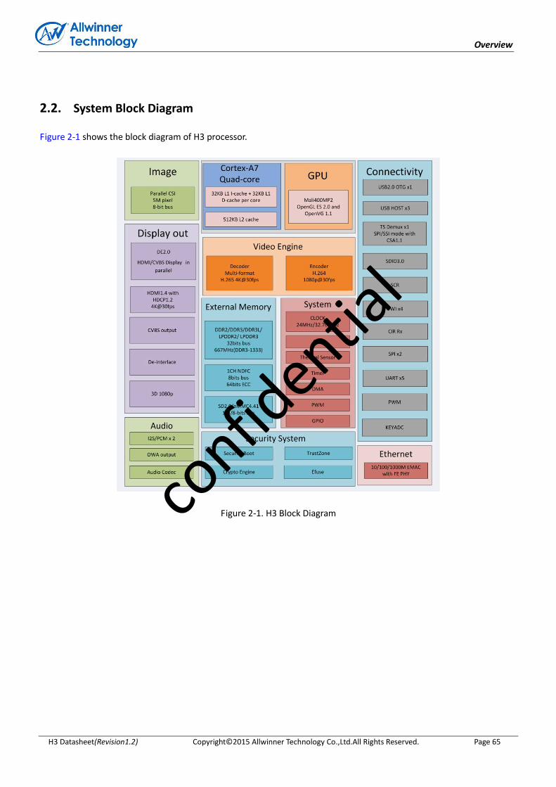
Overview
H3 Datasheet(Revision1.2) Copyright© 2015 Allwinner Technology Co.,Ltd.All Rights Reserved. Page 65
2.2. System Block Diagram
Figure 2-1 shows the block diagram of H3 processor.
Figure 2-1. H3 Block Diagram confid
ential

Pin Description
H3 Datasheet(Revision1.2) Copyright© 2015 Allwinner Technology Co.,Ltd.All Rights Reserved. Page 66
Chapter 3 Pin Description
3.1. Pin Characteristics
Table 3-1 lists the characteristics of H3 Pins from seven aspects: BALL#, Pin Name, Default Function, Type, Reset State,
Default Pull Up/Down, and Buffer Strength.
Table 3-1. Pin Characteristics
Ball# Pin Name Default
Function Type Reset State
Default
Pull Up/Down
Buffer Strength
(mA)
DRAM
T17 SA0 DRAM I/O Z - -
U18 SA1 DRAM I/O Z - -
V19 SA2 DRAM I/O Z - -
V20 SA3 DRAM I/O Z - -
V21 SA4 DRAM I/O Z - -
Y19 SA5 DRAM I/O Z - -
Y20 SA6 DRAM I/O Z - -
V15 SA7 DRAM I/O Z - -
W18 SA8 DRAM I/O Z - -
Y18 SA9 DRAM I/O Z - -
P19 SA10 DRAM I/O Z - -
N19 SA11 DRAM I/O Z - -
R18 SA12 DRAM I/O Z - -
V12 SA13 DRAM I/O Z - -
N17 SA14 DRAM I/O Z - -
R17 SA15 DRAM I/O Z - -
W17 SBA0 DRAM O Z - -
T18 SBA1 DRAM O Z - -
V17 SBA2 DRAM O Z - -
U15 SCAS DRAM O Z - -
AA19 SCK DRAM O Z - -
AA20 SCKB DRAM O Z - -
AA21 SCKE0 DRAM O Z - -
Y21 SCKE1 DRAM O Z - -
W20 SCS0 DRAM O Z - -
W21 SCS1 DRAM O Z - -
N20 SDQ0 DRAM I/O Z - -
P21 SDQ1 DRAM I/O Z - -
P20 SDQ2 DRAM I/O Z - -
confid
ential

Pin Description
H3 Datasheet(Revision1.2) Copyright© 2015 Allwinner Technology Co.,Ltd.All Rights Reserved. Page 67
Ball# Pin Name Default
Function Type Reset State
Default
Pull Up/Down
Buffer Strength
(mA)
U21 SDQ3 DRAM I/O Z - -
R19 SDQ4 DRAM I/O Z - -
T20 SDQ5 DRAM I/O Z - -
U19 SDQ6 DRAM I/O Z - -
U20 SDQ7 DRAM I/O Z - -
J19 SDQ8 DRAM I/O Z - -
H20 SDQ9 DRAM I/O Z - -
H21 SDQ10 DRAM I/O Z - -
J21 SDQ11 DRAM I/O Z - -
L20 SDQ12 DRAM I/O Z - -
L21 SDQ13 DRAM I/O Z - -
M21 SDQ14 DRAM I/O Z - -
M19 SDQ15 DRAM I/O Z - -
Y17 SDQ16 DRAM I/O Z - -
AA17 SDQ17 DRAM I/O Z - -
Y16 SDQ18 DRAM I/O Z - -
W15 SDQ19 DRAM I/O Z - -
Y14 SDQ20 DRAM I/O Z - -
AA14 SDQ21 DRAM I/O Z - -
Y13 SDQ22 DRAM I/O Z - -
Y12 SDQ23 DRAM I/O Z - -
W12 SDQ24 DRAM I/O Z - -
AA11 SDQ25 DRAM I/O Z - -
Y11 SDQ26 DRAM I/O Z - -
Y10 SDQ27 DRAM I/O Z - -
W9 SDQ28 DRAM I/O Z - -
AA8 SDQ29 DRAM I/O Z - -
Y8 SDQ30 DRAM I/O Z - -
Y7 SDQ31 DRAM I/O Z - -
M20 SDQM0 DRAM O Z - -
G20 SDQM1 DRAM O Z - -
AA18 SDQM2 DRAM O Z - -
AA12 SDQM3 DRAM O Z - -
R20 SDQS0 DRAM I/O Z - -
R21 SDQS0B DRAM I/O Z - -
K20 SDQS1 DRAM I/O Z - -
J20 SDQS1B DRAM I/O Z - -
AA15 SDQS2 DRAM I/O Z - -
Y15 SDQS2B DRAM I/O Z - -
AA9 SDQS3 DRAM I/O Z - -
Y9 SDQS3B DRAM I/O Z - -
confid
ential
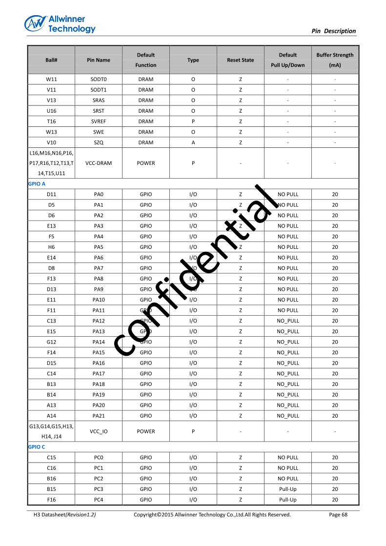
Pin Description
H3 Datasheet(Revision1.2) Copyright© 2015 Allwinner Technology Co.,Ltd.All Rights Reserved. Page 68
Ball# Pin Name Default
Function Type Reset State
Default
Pull Up/Down
Buffer Strength
(mA)
W11 SODT0 DRAM O Z - -
V11 SODT1 DRAM O Z - -
V13 SRAS DRAM O Z - -
U16 SRST DRAM O Z - -
T16 SVREF DRAM P Z - -
W13 SWE DRAM O Z - -
V10 SZQ DRAM A Z - -
L16,M16,N16,P16,
P17,R16,T12,T13,T
14,T15,U11
VCC-DRAM POWER P - - -
GPIO A
D11 PA0 GPIO I/O Z NO PULL 20
D5 PA1 GPIO I/O Z NO PULL 20
D6 PA2 GPIO I/O Z NO PULL 20
E13 PA3 GPIO I/O Z NO PULL 20
F5 PA4 GPIO I/O Z NO PULL 20
H6 PA5 GPIO I/O Z NO PULL 20
E14 PA6 GPIO I/O Z NO PULL 20
D8 PA7 GPIO I/O Z NO PULL 20
F13 PA8 GPIO I/O Z NO PULL 20
D13 PA9 GPIO I/O Z NO PULL 20
E11 PA10 GPIO I/O Z NO PULL 20
F11 PA11 GPIO I/O Z NO PULL 20
C13 PA12 GPIO I/O Z NO_PULL 20
E15 PA13 GPIO I/O Z NO_PULL 20
G12 PA14 GPIO I/O Z NO_PULL 20
F14 PA15 GPIO I/O Z NO_PULL 20
D15 PA16 GPIO I/O Z NO_PULL 20
C14 PA17 GPIO I/O Z NO_PULL 20
B13 PA18 GPIO I/O Z NO_PULL 20
B14 PA19 GPIO I/O Z NO_PULL 20
A13 PA20 GPIO I/O Z NO_PULL 20
A14 PA21 GPIO I/O Z NO_PULL 20
G13,G14,G15,H13,
H14, J14 VCC_IO POWER P - - -
GPIO C
C15 PC0 GPIO I/O Z NO PULL 20
C16 PC1 GPIO I/O Z NO PULL 20
B16 PC2 GPIO I/O Z NO PULL 20
B15 PC3 GPIO I/O Z Pull-Up 20
F16 PC4 GPIO I/O Z Pull-Up 20
confid
ential
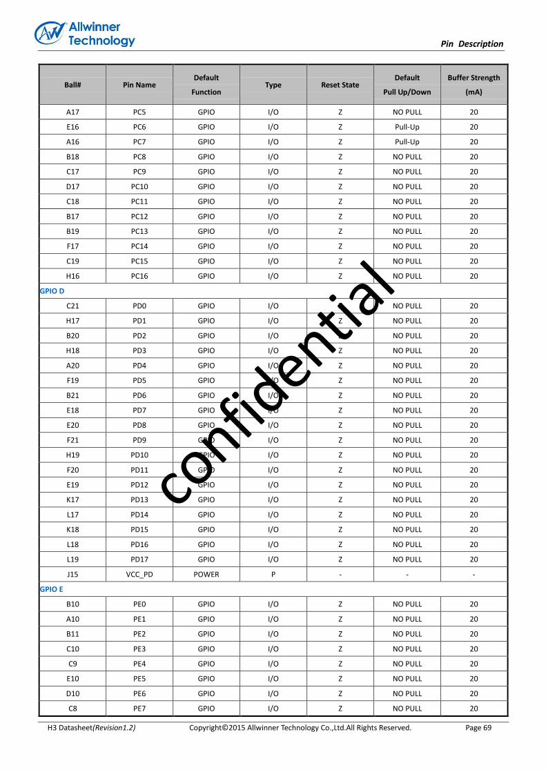
Pin Description
H3 Datasheet(Revision1.2) Copyright© 2015 Allwinner Technology Co.,Ltd.All Rights Reserved. Page 69
Ball# Pin Name Default
Function Type Reset State
Default
Pull Up/Down
Buffer Strength
(mA)
A17 PC5 GPIO I/O Z NO PULL 20
E16 PC6 GPIO I/O Z Pull-Up 20
A16 PC7 GPIO I/O Z Pull-Up 20
B18 PC8 GPIO I/O Z NO PULL 20
C17 PC9 GPIO I/O Z NO PULL 20
D17 PC10 GPIO I/O Z NO PULL 20
C18 PC11 GPIO I/O Z NO PULL 20
B17 PC12 GPIO I/O Z NO PULL 20
B19 PC13 GPIO I/O Z NO PULL 20
F17 PC14 GPIO I/O Z NO PULL 20
C19 PC15 GPIO I/O Z NO PULL 20
H16 PC16 GPIO I/O Z NO PULL 20
GPIO D
C21 PD0 GPIO I/O Z NO PULL 20
H17 PD1 GPIO I/O Z NO PULL 20
B20 PD2 GPIO I/O Z NO PULL 20
H18 PD3 GPIO I/O Z NO PULL 20
A20 PD4 GPIO I/O Z NO PULL 20
F19 PD5 GPIO I/O Z NO PULL 20
B21 PD6 GPIO I/O Z NO PULL 20
E18 PD7 GPIO I/O Z NO PULL 20
E20 PD8 GPIO I/O Z NO PULL 20
F21 PD9 GPIO I/O Z NO PULL 20
H19 PD10 GPIO I/O Z NO PULL 20
F20 PD11 GPIO I/O Z NO PULL 20
E19 PD12 GPIO I/O Z NO PULL 20
K17 PD13 GPIO I/O Z NO PULL 20
L17 PD14 GPIO I/O Z NO PULL 20
K18 PD15 GPIO I/O Z NO PULL 20
L18 PD16 GPIO I/O Z NO PULL 20
L19 PD17 GPIO I/O Z NO PULL 20
J15 VCC_PD POWER P - - -
GPIO E
B10 PE0 GPIO I/O Z NO PULL 20
A10 PE1 GPIO I/O Z NO PULL 20
B11 PE2 GPIO I/O Z NO PULL 20
C10 PE3 GPIO I/O Z NO PULL 20
C9 PE4 GPIO I/O Z NO PULL 20
E10 PE5 GPIO I/O Z NO PULL 20
D10 PE6 GPIO I/O Z NO PULL 20
C8 PE7 GPIO I/O Z NO PULL 20
confid
ential
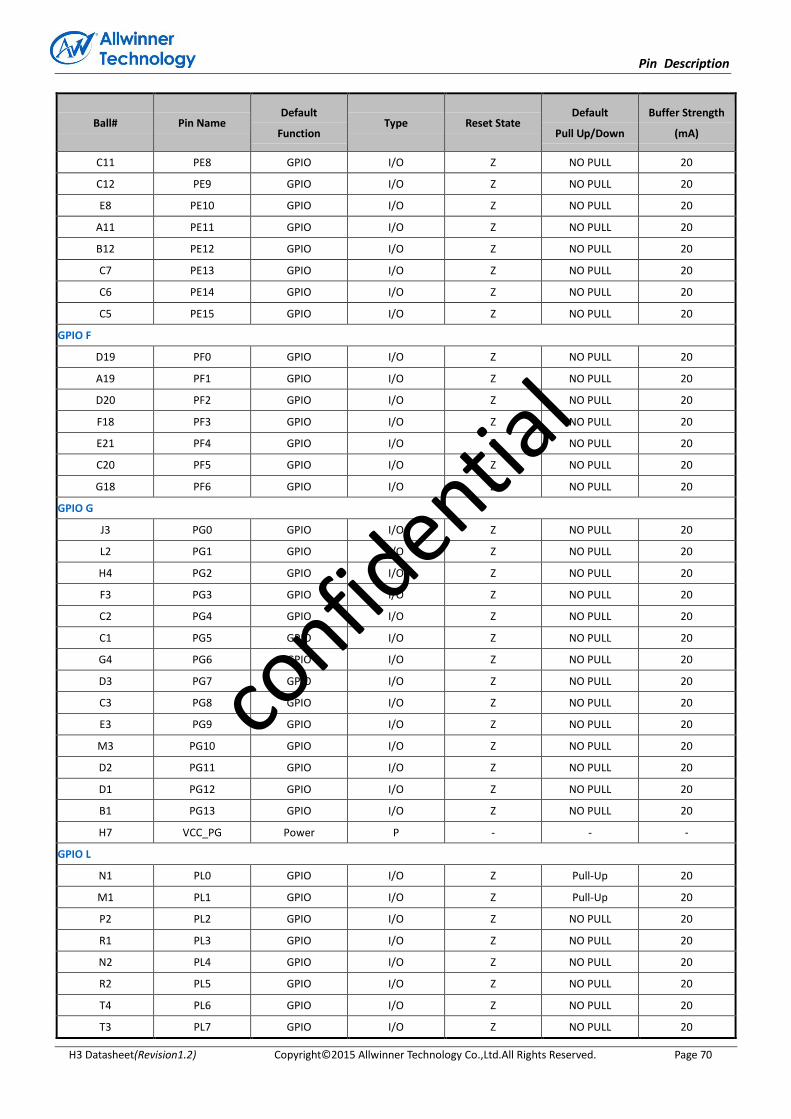
Pin Description
H3 Datasheet(Revision1.2) Copyright© 2015 Allwinner Technology Co.,Ltd.All Rights Reserved. Page 70
Ball# Pin Name Default
Function Type Reset State
Default
Pull Up/Down
Buffer Strength
(mA)
C11 PE8 GPIO I/O Z NO PULL 20
C12 PE9 GPIO I/O Z NO PULL 20
E8 PE10 GPIO I/O Z NO PULL 20
A11 PE11 GPIO I/O Z NO PULL 20
B12 PE12 GPIO I/O Z NO PULL 20
C7 PE13 GPIO I/O Z NO PULL 20
C6 PE14 GPIO I/O Z NO PULL 20
C5 PE15 GPIO I/O Z NO PULL 20
GPIO F
D19 PF0 GPIO I/O Z NO PULL 20
A19 PF1 GPIO I/O Z NO PULL 20
D20 PF2 GPIO I/O Z NO PULL 20
F18 PF3 GPIO I/O Z NO PULL 20
E21 PF4 GPIO I/O Z NO PULL 20
C20 PF5 GPIO I/O Z NO PULL 20
G18 PF6 GPIO I/O Z NO PULL 20
GPIO G
J3 PG0 GPIO I/O Z NO PULL 20
L2 PG1 GPIO I/O Z NO PULL 20
H4 PG2 GPIO I/O Z NO PULL 20
F3 PG3 GPIO I/O Z NO PULL 20
C2 PG4 GPIO I/O Z NO PULL 20
C1 PG5 GPIO I/O Z NO PULL 20
G4 PG6 GPIO I/O Z NO PULL 20
D3 PG7 GPIO I/O Z NO PULL 20
C3 PG8 GPIO I/O Z NO PULL 20
E3 PG9 GPIO I/O Z NO PULL 20
M3 PG10 GPIO I/O Z NO PULL 20
D2 PG11 GPIO I/O Z NO PULL 20
D1 PG12 GPIO I/O Z NO PULL 20
B1 PG13 GPIO I/O Z NO PULL 20
H7 VCC_PG Power P - - -
GPIO L
N1 PL0 GPIO I/O Z Pull-Up 20
M1 PL1 GPIO I/O Z Pull-Up 20
P2 PL2 GPIO I/O Z NO PULL 20
R1 PL3 GPIO I/O Z NO PULL 20
N2 PL4 GPIO I/O Z NO PULL 20
R2 PL5 GPIO I/O Z NO PULL 20
T4 PL6 GPIO I/O Z NO PULL 20
T3 PL7 GPIO I/O Z NO PULL 20
confid
ential
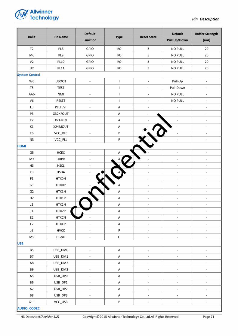
Pin Description
H3 Datasheet(Revision1.2) Copyright© 2015 Allwinner Technology Co.,Ltd.All Rights Reserved. Page 71
Ball# Pin Name Default
Function Type Reset State
Default
Pull Up/Down
Buffer Strength
(mA)
T2 PL8 GPIO I/O Z NO PULL 20
M6 PL9 GPIO I/O Z NO PULL 20
V2 PL10 GPIO I/O Z NO PULL 20
U2 PL11 GPIO I/O Z NO PULL 20
System Control
W6 UBOOT - I - Pull-Up -
T5 TEST - I - Pull-Down -
AA6 NMI - I - NO PULL -
V6 RESET - I - NO PULL -
L5 PLLTEST - A - - -
P3 X32KFOUT - A - - -
K2 X24MIN - A - - -
K1 X24MOUT - A - - -
K6 VCC_RTC - P - - -
N3 VCC_PLL - P - - -
HDMI
G5 HCEC - A - - -
M2 HHPD - A - - -
H3 HSCL - A - - -
K3 HSDA - A - - -
F1 HTX0N - A - - -
G1 HTX0P - A - - -
G2 HTX1N - A - - -
H2 HTX1P - A - - -
J2 HTX2N - A - - -
J1 HTX2P - A - - -
E2 HTXCN - A - - -
F2 HTXCP - A - - -
J6 HVCC - P - - -
M5 HGND - G - - -
USB
B5 USB_DM0 - A - - -
B7 USB_DM1 - A - - -
A8 USB_DM2 - A - - -
B9 USB_DM3 - A - - -
A5 USB_DP0 - A - - -
B6 USB_DP1 - A - - -
A7 USB_DP2 - A - - -
B8 USB_DP3 - A - - -
G11 VCC_USB - P - - -
AUDIO_CODEC
confid
ential
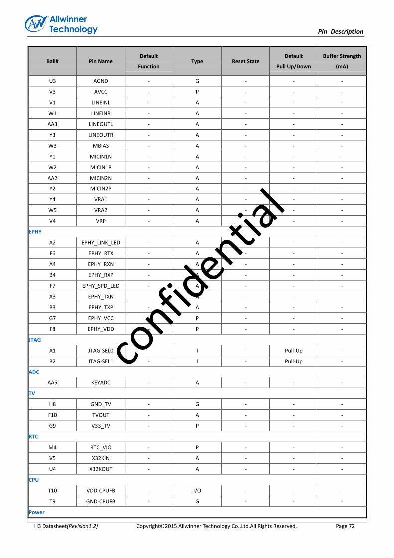
Pin Description
H3 Datasheet(Revision1.2) Copyright© 2015 Allwinner Technology Co.,Ltd.All Rights Reserved. Page 72
Ball# Pin Name Default
Function Type Reset State
Default
Pull Up/Down
Buffer Strength
(mA)
U3 AGND - G - - -
V3 AVCC - P - - -
V1 LINEINL - A - - -
W1 LINEINR - A - - -
AA3 LINEOUTL - A - - -
Y3 LINEOUTR - A - - -
W3 MBIAS - A - - -
Y1 MICIN1N - A - - -
W2 MICIN1P - A - - -
AA2 MICIN2N - A - - -
Y2 MICIN2P - A - - -
Y4 VRA1 - A - - -
W5 VRA2 - A - - -
V4 VRP - A - - -
EPHY
A2 EPHY_LINK_LED - A - - -
F6 EPHY_RTX - A - - -
A4 EPHY_RXN - A - - -
B4 EPHY_RXP - A - - -
F7 EPHY_SPD_LED - A - - -
A3 EPHY_TXN - A - - -
B3 EPHY_TXP - A - - -
G7 EPHY_VCC - P - - -
F8 EPHY_VDD - P - - -
JTAG
A1 JTAG-SEL0 - I - Pull-Up -
B2 JTAG-SEL1 - I - Pull-Up -
ADC
AA5 KEYADC - A - - -
TV
H8 GND_TV - G - - -
F10 TVOUT - A - - -
G9 V33_TV - P - - -
RTC
M4 RTC_VIO - P - - -
V5 X32KIN - A - - -
U4 X32KOUT - A - - -
CPU
T10 VDD-CPUFB - I/O - - -
T9 GND-CPUFB - G - - -
Power
confid
ential

Pin Description
H3 Datasheet(Revision1.2) Copyright© 2015 Allwinner Technology Co.,Ltd.All Rights Reserved. Page 73
Ball# Pin Name Default
Function Type Reset State
Default
Pull Up/Down
Buffer Strength
(mA)
H11 VDD_EFUSEEBP - P - - -
G10 VDD_EFUSE - P - - -
N8,P6,P7,P8,P9,R6,
R7, R8,T6,T7,
T8,U6,U9
VDD_CPUX - P - - -
J7,J8 VDD_CPUS - P - - -
H10,J10,J11,J12,K1
0,K11,K12,L10,L11,
L12,L13, L14
VDD-SYS - P - - -
A21,AA1,G8,H12,
H15, J13,J16, J9,
K13, K14,K15, K16,
K7,K8,K9,L15,L8,L9,
M10,M11,M12,
M13,M14,M15,M7,
M8,M9,N10,N11,
N12,N13,N14,N15,
N7,N9,P10,P11,P12
,.P13,P14,P15,R10,
R11,R12,R13,R14,
R9,T11
GND - G - - -
Other
K4 NC - - - - -
Note:
1) Default Function defines the default function of each pin, especially for pins with multiplexing functions;
2) Type defines the signal direction: I (Input), O (Output), I/O(Input / Output), OD(Open-Drain), A (Analog), AI(Analog
Input), AO(Analog Output),A I/O(Analog Input /Output), P (Power), G (Ground);
3) Reset State defines the state of the terminal at reset: Z for high-impedance ;
4) Default Pull Up/Down defines the presence of an internal pull up or pull down resister. Unless otherwise specified,
the pin is default to be floating, and can be configured as pull up or pull down;
5) Buffer Strength defines drive strength of the associated output buffer.
confid
ential

Pin Description
H3 Datasheet(Revision1.2) Copyright© 2015 Allwinner Technology Co.,Ltd.All Rights Reserved. Page 74
3.2. GPIO Multiplexing Functions
Table 3-2 provides a description of the H3 GPIO multiplexing functions.
Table 3-2. Multiplexing Functions
Pin
Name
Default
Function
IO
Type
Default
IO State
Default
Pull-up/
down
Function 2 Function3 Function 4 Function 5 Function 6
PA0
GPIO
I/O DIS Z UART2_TX JTAG_MS - - PA_EINT0
PA1 I/O DIS Z UART2_RX JTAG_CK - - PA_EINT1
PA2 I/O DIS Z UART2_RTS JTAG_DO - - PA_EINT2
PA3 I/O DIS Z UART2_CTS JTAG_DI - - PA_EINT3
PA4 I/O DIS Z UART0_TX - - - PA_EINT4
PA5 I/O DIS Z UART0_RX PWM0 - - PA_EINT5
PA6 I/O DIS Z SIM_PWREN - - - PA_EINT6
PA7 I/O DIS Z SIM_CLK - - - PA_EINT7
PA8 I/O DIS Z SIM_DATA - - - PA_EINT8
PA9 I/O DIS Z SIM_RST - - - PA_EINT9
PA10 I/O DIS Z SIM_DET - - - PA_EINT10
PA11 I/O DIS Z TWI0_SCK DI_TX - - PA_EINT11
PA12 I/O DIS Z TWI0_SDA DI_RX - - PA_EINT12
PA13 I/O DIS Z SPI1_CS UART3_TX - - PA_EINT13
PA14 I/O DIS Z SPI1_CLK UART3_RX - - PA_EINT14
PA15 I/O DIS Z SPI1_MOSI UART3_RTS - - PA_EINT15
PA16 I/O DIS Z SPI1_MISO UART3_CTS - - PA_EINT16
PA17 I/O DIS Z OWA_OUT - - - PA_EINT17
PA18 I/O DIS Z PCM0_SYNC TWI1_SCK - - PA_EINT18
PA19 I/O DIS Z PCM0_CLK TWI1_SDA - - PA_EINT19
PA20 I/O DIS Z PCM0_DOUT SIM_VPPEN - - PA_EINT20
PA21 I/O DIS Z PCM0_DIN SIM_VPPPP - - PA_EINT21
PC0
GPIO
I/O DIS Z NAND_WE SPI0_MOSI - - -
PC1 I/O DIS Z NAND_ALE SPI0_MISO - - -
PC2 I/O DIS Z NAND_CLE SPI0_CLK - - -
PC3 I/O DIS Pull-up NAND_CE1 SPI0_CS - - -
PC4 I/O DIS Pull-up NAND_CE0 - - - -
PC5 I/O DIS Z NAND_RE SDC2_CLK - - -
PC6 I/O DIS Pull-up NAND_RB0 SDC2_CMD - - -
PC7 I/O DIS Pull-up NAND_RB1 - - - -
PC8 I/O DIS Z NAND_DQ0 SDC2_D0 - - -
PC9 I/O DIS Z NAND_DQ1 SDC2_D1 - - -
PC10 I/O DIS Z NAND_DQ2 SDC2_D2 - - -
PC11 I/O DIS Z NAND_DQ3 SDC2_D3 - - -
confid
ential

Pin Description
H3 Datasheet(Revision1.2) Copyright© 2015 Allwinner Technology Co.,Ltd.All Rights Reserved. Page 75
Pin
Name
Default
Function
IO
Type
Default
IO State
Default
Pull-up/
down
Function 2 Function3 Function 4 Function 5 Function 6
PC12 I/O DIS Z NAND_DQ4 SDC2_D4 - - -
PC13 I/O DIS Z NAND_DQ5 SDC2_D5 - - -
PC14 I/O DIS Z NAND_DQ6 SDC2_D6 - - -
PC15 I/O DIS Z NAND_DQ7 SDC2_D7 - - -
PC16 I/O DIS Z NAND_DQS SDC2_RST - - -
PD0
GPIO
I/O DIS Z
RGMII_RXD3/
MII_RXD3/
RMII_NULL
- - - -
PD1 I/O DIS Z
RGMII_RXD2/
MII_RXD2/RM
II_NULL
- - - -
PD2 I/O DIS Z
RGMII_RXD1/
MII_RXD2/RM
II_RXD1
- - - -
PD3 I/O DIS Z
RGMII_RXD0/
MII_RXD1/RM
II_RXD0
- - - -
PD4 I/O DIS Z
RGMII_RXCK/
MII_RXCK/RMI
I_NULL
- - - -
PD5 I/O DIS Z
RGMII_RXCTL/
MII_RXDV/RM
II_NULL
- - - -
PD6 I/O DIS Z
RGMII_NULL/
MII_RXERR/R
MII_RXER
- - - -
PD7 I/O DIS Z
RGMII_TXD3/
MII_TXD3/RMI
I_NULL
- - - -
PD8 I/O DIS Z
RGMII_TXD2/
MII_TXD2/RMI
I_NULL
- - - -
PD9 I/O DIS Z
RGMII_TXD1/
MII_TXD1/RMI
I_TXD1
- - - -
PD10 I/O DIS Z
RGMII_TXD0/
MII_TXD0/RMI
I_TXD0
- - - -
PD11 I/O DIS Z
RGMII_NULL/
MII_CRS/RMII
_CRS_DV
- - - -
PD12 I/O DIS Z RGMII_TXCK/ - - - -
confid
ential
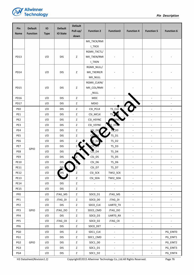
Pin Description
H3 Datasheet(Revision1.2) Copyright© 2015 Allwinner Technology Co.,Ltd.All Rights Reserved. Page 76
Pin
Name
Default
Function
IO
Type
Default
IO State
Default
Pull-up/
down
Function 2 Function3 Function 4 Function 5 Function 6
MII_TXCK/RMI
I_TXCK
PD13 I/O DIS Z
RGMII_TXCTL/
MII_TXEN/RMI
I_TXEN
- - - -
PD14 I/O DIS Z
RGMII_NULL/
MII_TXERR/R
MII_NULL
- - - -
PD15 I/O DIS Z
RGMII_CLKIN/
MII_COL/RMII
_NULL
- - - -
PD16 I/O DIS Z MDC - - - -
PD17 I/O DIS Z MDIO - - - -
PE0
GPIO
I/O DIS Z CSI_PCLK TS_CLK - - -
PE1 I/O DIS Z CSI_MCLK TS_ERR - - -
PE2 I/O DIS Z CSI_HSYNC TS_SYNC - - -
PE3 I/O DIS Z CSI_VSYNC TS_DVLD - - -
PE4 I/O DIS Z CSI_D0 TS_D0 - - -
PE5 I/O DIS Z CSI_D1 TS_D1 - - -
PE6 I/O DIS Z CSI_D2 TS_D2 - - -
PE7 I/O DIS Z CSI_D3 TS_D3 - - -
PE8 I/O DIS Z CSI_D4 TS_D4 - - -
PE9 I/O DIS Z CSI_D5 TS_D5 - - -
PE10 I/O DIS Z CSI_D6 TS_D6 - - -
PE11 I/O DIS Z CSI_D7 TS_D7 - - -
PE12 I/O DIS Z CSI_SCK TWI2_SCK - - -
PE13 I/O DIS Z CSI_SDA TWI2_SDA - - -
PE14 I/O DIS Z - - - - -
PE15 I/O DIS Z - - - - -
PF0
GPIO
I/O JTAG_MS Z SDC0_D1 JTAG_MS - - -
PF1 I/O JTAG_DI Z SDC0_D0 JTAG_DI - - -
PF2 I/O DIS Z SDC0_CLK UART0_TX - - -
PF3 I/O JTAG_DO Z SDC0_CMD JTAG_DO - - -
PF4 I/O DIS Z SDC0_D3 UART0_RX - - -
PF5 I/O JTAG_CK Z SDC0_D2 JTAG_CK - - -
PF6 I/O DIS Z SDC0_DET - - - -
PG0
GPIO
I/O DIS Z SDC1_CLK - - - PG_EINT0
PG1 I/O DIS Z SDC1_CMD - - - PG_EINT1
PG2 I/O DIS Z SDC1_D0 - - - PG_EINT2
PG3 I/O DIS Z SDC1_D1 - - - PG_EINT3
PG4 I/O DIS Z SDC1_D2 - - - PG_EINT4
confid
ential

Pin Description
H3 Datasheet(Revision1.2) Copyright© 2015 Allwinner Technology Co.,Ltd.All Rights Reserved. Page 77
Pin
Name
Default
Function
IO
Type
Default
IO State
Default
Pull-up/
down
Function 2 Function3 Function 4 Function 5 Function 6
PG5 I/O DIS Z SDC1_D3 - - - PG_EINT5
PG6 I/O DIS Z UART1_TX - - - PG_EINT6
PG7 I/O DIS Z UART1_RX - - - PG_EINT7
PG8 I/O DIS Z UART1_RTS - - - PG_EINT8
PG9 I/O DIS Z UART1_CTS - - - PG_EINT9
PG10 I/O DIS Z PCM1_SYNC - - - PG_EINT10
PG11 I/O DIS Z PCM1_CLK - - - PG_EINT11
PG12 I/O DIS Z PCM1_DOUT - - - PG_EINT12
PG13 I/O DIS Z PCM1_DIN - - - PG_EINT13
PL0
GPIO
I/O DIS Pull-up S_TWI_SCK - - - S_PL_EINT0
PL1 I/O DIS Pull-up S_TWI_SDA - - - S_PL_EINT1
PL2 I/O DIS Z S_UART_TX - - - S_PL_EINT2
PL3 I/O DIS Z S_UART_RX - - - S_PL_EINT3
PL4 I/O DIS Z S_JTAG_MS - - - S_PL_EINT4
PL5 I/O DIS Z S_JTAG_CK - - - S_PL_EINT5
PL6 I/O DIS Z S_JTAG_DO - - - S_PL_EINT6
PL7 I/O DIS Z S_JTAG_DI - - - S_PL_EINT7
PL8 I/O DIS Z - - - - S_PL_EINT8
PL9 I/O DIS Z - - - - S_PL_EINT9
PL10 I/O DIS Z S_PWM - - - S_PL_EINT10
PL11 I/O DIS Z S_CIR_RX - - - S_PL_EINT12
confid
ential
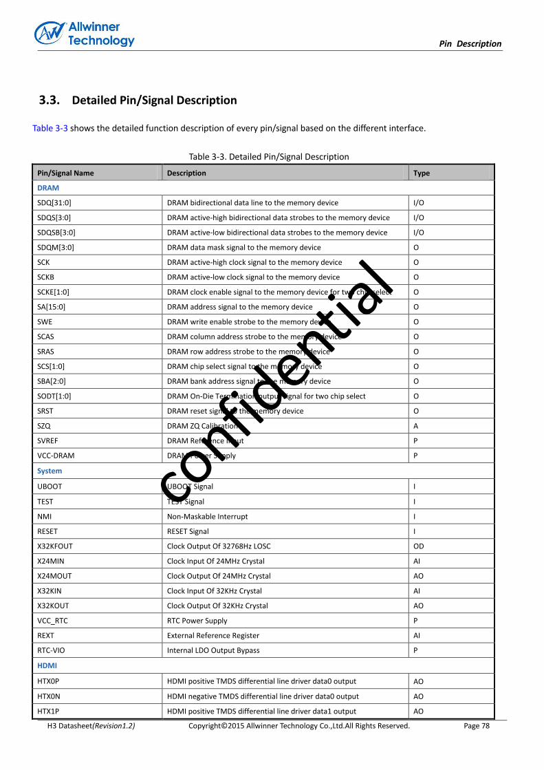
Pin Description
H3 Datasheet(Revision1.2) Copyright© 2015 Allwinner Technology Co.,Ltd.All Rights Reserved. Page 78
3.3. Detailed Pin/Signal Description
Table 3-3 shows the detailed function description of every pin/signal based on the different interface.
Table 3-3. Detailed Pin/Signal Description
Pin/Signal Name Description Type
DRAM
SDQ[31:0] DRAM bidirectional data line to the memory device I/O
SDQS[3:0] DRAM active-high bidirectional data strobes to the memory device I/O
SDQSB[3:0] DRAM active-low bidirectional data strobes to the memory device I/O
SDQM[3:0] DRAM data mask signal to the memory device O
SCK DRAM active-high clock signal to the memory device O
SCKB DRAM active-low clock signal to the memory device O
SCKE[1:0] DRAM clock enable signal to the memory device for two chip select O
SA[15:0] DRAM address signal to the memory device O
SWE DRAM write enable strobe to the memory device O
SCAS DRAM column address strobe to the memory device O
SRAS DRAM row address strobe to the memory device O
SCS[1:0] DRAM chip select signal to the memory device O
SBA[2:0] DRAM bank address signal to the memory device O
SODT[1:0] DRAM On-Die Termination output signal for two chip select O
SRST DRAM reset signal to the memory device O
SZQ DRAM ZQ Calibration A
SVREF DRAM Reference Input P
VCC-DRAM DRAM Power Supply P
System
UBOOT UBOOT Signal I
TEST TEST Signal I
NMI Non-Maskable Interrupt I
RESET RESET Signal I
X32KFOUT Clock Output Of 32768Hz LOSC OD
X24MIN Clock Input Of 24MHz Crystal AI
X24MOUT Clock Output Of 24MHz Crystal AO
X32KIN Clock Input Of 32KHz Crystal AI
X32KOUT Clock Output Of 32KHz Crystal AO
VCC_RTC RTC Power Supply P
REXT External Reference Register AI
RTC-VIO Internal LDO Output Bypass P
HDMI
HTX0P HDMI positive TMDS differential line driver data0 output AO
HTX0N HDMI negative TMDS differential line driver data0 output AO
HTX1P HDMI positive TMDS differential line driver data1 output AO
confid
ential
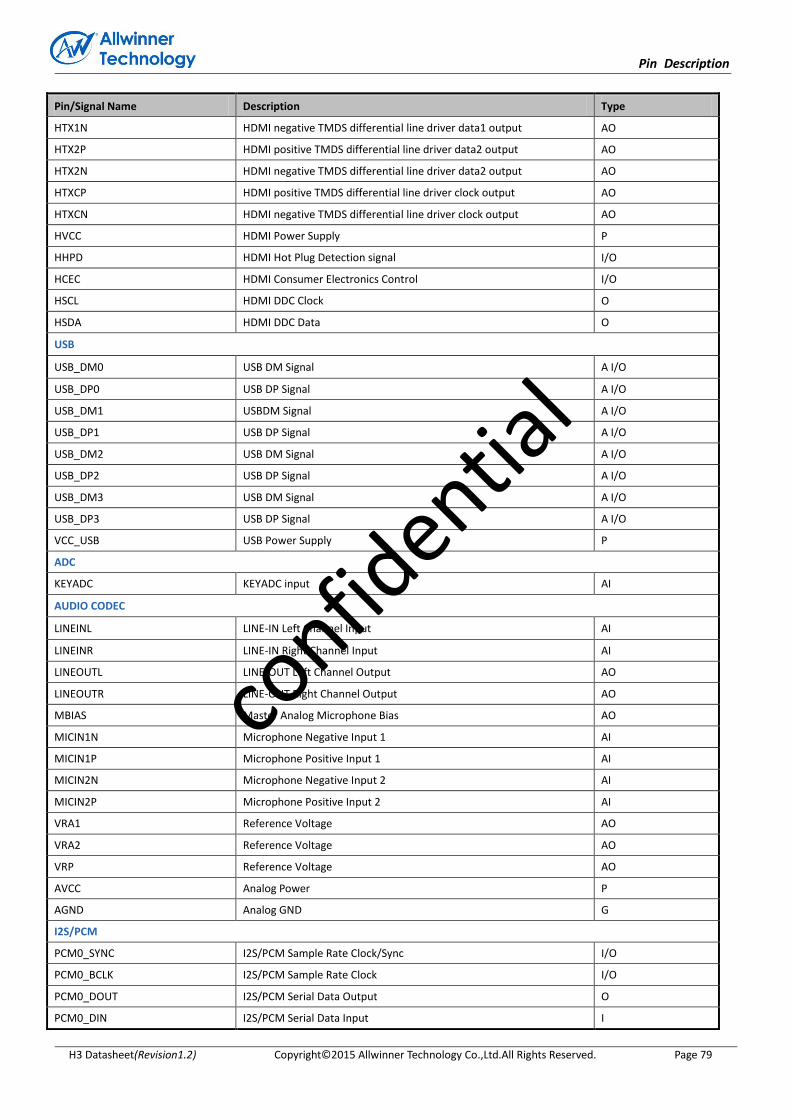
Pin Description
H3 Datasheet(Revision1.2) Copyright© 2015 Allwinner Technology Co.,Ltd.All Rights Reserved. Page 79
Pin/Signal Name Description Type
HTX1N HDMI negative TMDS differential line driver data1 output AO
HTX2P HDMI positive TMDS differential line driver data2 output AO
HTX2N HDMI negative TMDS differential line driver data2 output AO
HTXCP HDMI positive TMDS differential line driver clock output AO
HTXCN HDMI negative TMDS differential line driver clock output AO
HVCC HDMI Power Supply P
HHPD HDMI Hot Plug Detection signal I/O
HCEC HDMI Consumer Electronics Control I/O
HSCL HDMI DDC Clock O
HSDA HDMI DDC Data O
USB
USB_DM0 USB DM Signal A I/O
USB_DP0 USB DP Signal A I/O
USB_DM1 USBDM Signal A I/O
USB_DP1 USB DP Signal A I/O
USB_DM2 USB DM Signal A I/O
USB_DP2 USB DP Signal A I/O
USB_DM3 USB DM Signal A I/O
USB_DP3 USB DP Signal A I/O
VCC_USB USB Power Supply P
ADC
KEYADC KEYADC input AI
AUDIO CODEC
LINEINL LINE-IN Left Channel Input AI
LINEINR LINE-IN Right Channel Input AI
LINEOUTL LINE-OUT Left Channel Output AO
LINEOUTR LINE-OUT Right Channel Output AO
MBIAS Master Analog Microphone Bias AO
MICIN1N Microphone Negative Input 1 AI
MICIN1P Microphone Positive Input 1 AI
MICIN2N Microphone Negative Input 2 AI
MICIN2P Microphone Positive Input 2 AI
VRA1 Reference Voltage AO
VRA2 Reference Voltage AO
VRP Reference Voltage AO
AVCC Analog Power P
AGND Analog GND G
I2S/PCM
PCM0_SYNC I2S/PCM Sample Rate Clock/Sync I/O
PCM0_BCLK I2S/PCM Sample Rate Clock I/O
PCM0_DOUT I2S/PCM Serial Data Output O
PCM0_DIN I2S/PCM Serial Data Input I
confid
ential
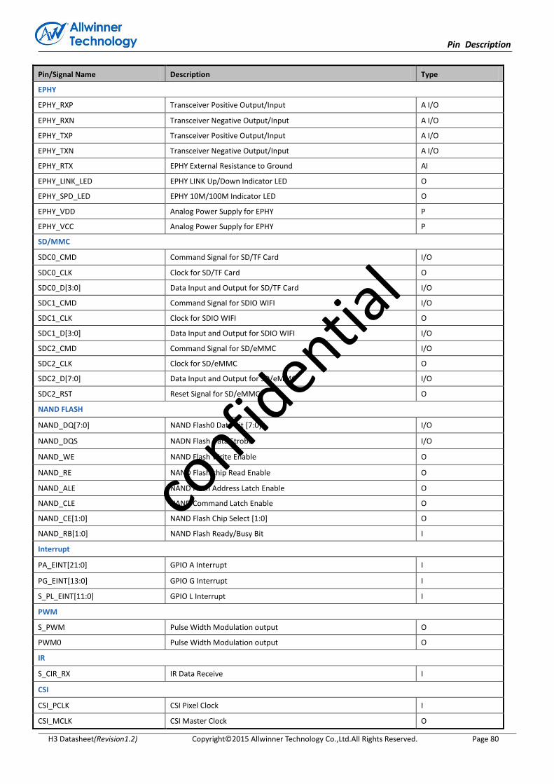
Pin Description
H3 Datasheet(Revision1.2) Copyright© 2015 Allwinner Technology Co.,Ltd.All Rights Reserved. Page 80
Pin/Signal Name Description Type
EPHY
EPHY_RXP Transceiver Positive Output/Input A I/O
EPHY_RXN Transceiver Negative Output/Input A I/O
EPHY_TXP Transceiver Positive Output/Input A I/O
EPHY_TXN Transceiver Negative Output/Input A I/O
EPHY_RTX EPHY External Resistance to Ground AI
EPHY_LINK_LED EPHY LINK Up/Down Indicator LED O
EPHY_SPD_LED EPHY 10M/100M Indicator LED O
EPHY_VDD Analog Power Supply for EPHY P
EPHY_VCC Analog Power Supply for EPHY P
SD/MMC
SDC0_CMD Command Signal for SD/TF Card I/O
SDC0_CLK Clock for SD/TF Card O
SDC0_D[3:0] Data Input and Output for SD/TF Card I/O
SDC1_CMD Command Signal for SDIO WIFI I/O
SDC1_CLK Clock for SDIO WIFI O
SDC1_D[3:0] Data Input and Output for SDIO WIFI I/O
SDC2_CMD Command Signal for SD/eMMC I/O
SDC2_CLK Clock for SD/eMMC O
SDC2_D[7:0] Data Input and Output for SD/eMMC I/O
SDC2_RST Reset Signal for SD/eMMC O
NAND FLASH
NAND_DQ[7:0] NAND Flash0 Data Bit [7:0] I/O
NAND_DQS NADN Flash Data Strobe I/O
NAND_WE NAND Flash Write Enable O
NAND_RE NAND Flash chip Read Enable O
NAND_ALE NAND Flash Address Latch Enable O
NAND_CLE NAND Command Latch Enable O
NAND_CE[1:0] NAND Flash Chip Select [1:0] O
NAND_RB[1:0] NAND Flash Ready/Busy Bit I
Interrupt
PA_EINT[21:0] GPIO A Interrupt I
PG_EINT[13:0] GPIO G Interrupt I
S_PL_EINT[11:0] GPIO L Interrupt I
PWM
S_PWM Pulse Width Modulation output O
PWM0 Pulse Width Modulation output O
IR
S_CIR_RX IR Data Receive I
CSI
CSI_PCLK CSI Pixel Clock I
CSI_MCLK CSI Master Clock O
confid
ential
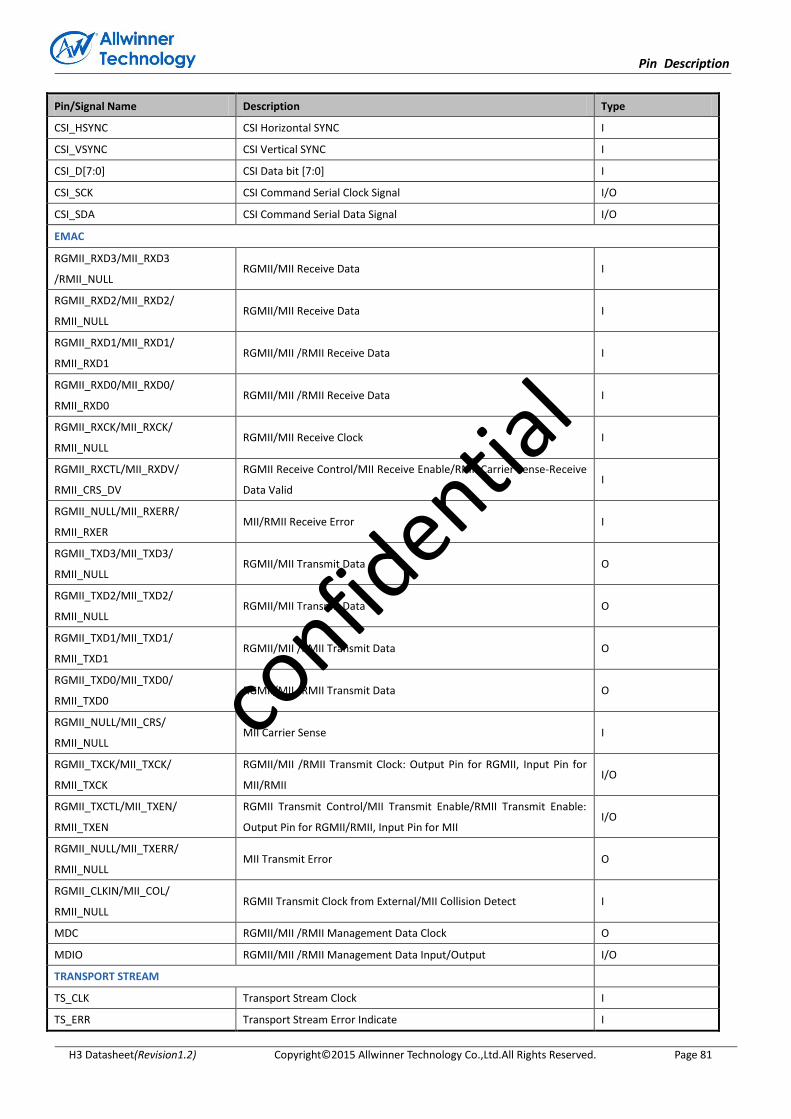
Pin Description
H3 Datasheet(Revision1.2) Copyright© 2015 Allwinner Technology Co.,Ltd.All Rights Reserved. Page 81
Pin/Signal Name Description Type
CSI_HSYNC CSI Horizontal SYNC I
CSI_VSYNC CSI Vertical SYNC I
CSI_D[7:0] CSI Data bit [7:0] I
CSI_SCK CSI Command Serial Clock Signal I/O
CSI_SDA CSI Command Serial Data Signal I/O
EMAC
RGMII_RXD3/MII_RXD3
/RMII_NULL RGMII/MII Receive Data I
RGMII_RXD2/MII_RXD2/
RMII_NULL RGMII/MII Receive Data I
RGMII_RXD1/MII_RXD1/
RMII_RXD1 RGMII/MII /RMII Receive Data I
RGMII_RXD0/MII_RXD0/
RMII_RXD0 RGMII/MII /RMII Receive Data I
RGMII_RXCK/MII_RXCK/
RMII_NULL RGMII/MII Receive Clock I
RGMII_RXCTL/MII_RXDV/
RMII_CRS_DV
RGMII Receive Control/MII Receive Enable/RMII Carrier Sense-Receive
Data Valid I
RGMII_NULL/MII_RXERR/
RMII_RXER MII/RMII Receive Error I
RGMII_TXD3/MII_TXD3/
RMII_NULL RGMII/MII Transmit Data O
RGMII_TXD2/MII_TXD2/
RMII_NULL RGMII/MII Transmit Data O
RGMII_TXD1/MII_TXD1/
RMII_TXD1 RGMII/MII /RMII Transmit Data O
RGMII_TXD0/MII_TXD0/
RMII_TXD0 RGMII/MII /RMII Transmit Data O
RGMII_NULL/MII_CRS/
RMII_NULL MII Carrier Sense I
RGMII_TXCK/MII_TXCK/
RMII_TXCK
RGMII/MII /RMII Transmit Clock: Output Pin for RGMII, Input Pin for
MII/RMII I/O
RGMII_TXCTL/MII_TXEN/
RMII_TXEN
RGMII Transmit Control/MII Transmit Enable/RMII Transmit Enable:
Output Pin for RGMII/RMII, Input Pin for MII I/O
RGMII_NULL/MII_TXERR/
RMII_NULL MII Transmit Error O
RGMII_CLKIN/MII_COL/
RMII_NULL RGMII Transmit Clock from External/MII Collision Detect I
MDC RGMII/MII /RMII Management Data Clock O
MDIO RGMII/MII /RMII Management Data Input/Output I/O
TRANSPORT STREAM
TS_CLK Transport Stream Clock I
TS_ERR Transport Stream Error Indicate I
confid
ential

Pin Description
H3 Datasheet(Revision1.2) Copyright© 2015 Allwinner Technology Co.,Ltd.All Rights Reserved. Page 82
Pin/Signal Name Description Type
TS_SYNC Transport Stream Sync I
TS_DVLD Transport Stream Valid Signal I
TS_D[7:0] Transport Stream Data I
SPI (x=[1:0])
SPIx_CS SPIx Chip Select signal, low active I/O
SPIx_CLK SPIx Clock signal I/O
SPIx_MOSI SPIx Master data Out, Slave data In I/O
SPIx_MISO SPIx Master data In, Slave data Out I/O
UART
UART0_TX UART0 Data Transmit O
UART0_RX UART0 Data Receive I
UART1_TX UART1 Data Transmit O
UART1_RX UART1 Data Receive I
UART1_CTS UART1 Data Clear To Send I
UART1_RTS UART1 Data Request To Send O
UART2_TX UART2 Data Transmit O
UART2_RX UART2 Data Receive I
UART2_CTS UART2 Data Clear To Send I
UART2_RTS UART2 Data Request To Send O
UART3_TX UART3 Data Transmit O
UART3_RX UART3 Data Receive I
UART3_CTS UART3 Data Clear To Send I
UART3_RTS UART3 Data Request To Send O
S_UART_TX UART Data Transmit O
S_UART_RX UART Data Receive I
TWI (x=[2:0])
TWIx_SCK TWIx Serial Clock Signal I/O
TWIx_SDA TWIx Serial Data Signal I/O
S_TWI_SCK TWI Serial Clock Signal I/O
S_TWI_SDA TWI Serial Data Signal I/O
confid
ential
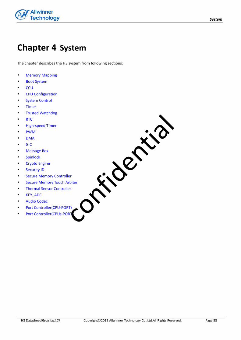
System
H3 Datasheet(Revision1.2) Copyright© 2015 Allwinner Technology Co.,Ltd.All Rights Reserved. Page 83
Chapter 4 System
The chapter describes the H3 system from following sections:
Memory Mapping
Boot System
CCU
CPU Configuration
System Control
Timer
Trusted Watchdog
RTC
High-speed Timer
PWM
DMA
GIC
Message Box
Spinlock
Crypto Engine
Security ID
Secure Memory Controller
Secure Memory Touch Arbiter
Thermal Sensor Controller
KEY_ADC
Audio Codec
Port Controller(CPU-PORT)
Port Controller(CPUs-PORT)
co
nfidentia
l

System
H3 Datasheet(Revision1.2) Copyright© 2015 Allwinner Technology Co.,Ltd.All Rights Reserved. Page 84
4.1. Memory Mapping
Module Address (It is for Cluster CPU) Size (byte)
SRAM A1 0x0000 0000---0x0000 FFFF 64K
SRAM A2 0x0004 4000---0x0004 BFFF 32K
SRAM C 0x0001 0000---0x0001 AFFF 44K
DE 0x0100 0000---0x013F FFFF 4M
De-interlaced 0x0140 0000---0x0141 FFFF 128K
System Control 0x01C0 0000---0x01C0 0FFF 4K
DMA 0x01C0 2000---0x01C0 2FFF 4K
NFDC 0x01C0 3000---0x01C0 3FFF 4K
TS 0x01C0 6000---0x01C0 6FFF 4K
Key Memory Space 0x01C0 B000---0x01C0 BFFF 4K
LCD 0 0x01C0 C000---0x01C0 CFFF 4K
LCD 1 0x01C0 D000---0x01C0 DFFF 4K
VE 0x01C0 E000---0x01C0 EFFF 4K
SD/MMC 0 0x01C0 F000---0x01C0 FFFF 4K
SD/MMC 1 0x01C1 0000---0x01C1 0FFF 4K
SD/MMC 2 0x01C1 1000---0x01C1 1FFF 4K
SID 0x01C1 4000---0x01C1 43FF 1K
Crypto Engine 0x01C1 5000---0x01C1 5FFF 4K
MSG_BOX 0x01C1 7000---0x01C1 7FFF 4K
SPINLOCK 0x01C1 8000---0x01C1 8FFF 4K
USB-OTG_Device 0x01C1 9000---0x01C1 9FFF 4K
USB-OTG_EHCI0/OHCI0 0x01C1 A000---0x01C1 AFFF 4K
USB-HCI1 0x01C1 B000---0x01C1 BFFF 4K
USB-HCI2 0x01C1 C000---0x01C1 CFFF 4K
USB-HCI3 0x01C1 D000---0x01C1 DFFF 4K
SMC 0x01C1 E000---0x01C1 EFFF 4K
CCU 0x01C2 0000---0x01C2 03FF 1K
PIO 0x01C2 0800---0x01C2 0BFF 1K
TIMER 0x01C2 0C00---0x01C2 0FFF 1K
OWA 0x01C2 1000---0x01C2 13FF 1K
PWM 0x01C2 1400---0x01C2 17FF 1K
KEYADC 0x01C2 1800---0x01C2 1BFF 1K
I2S/PCM 0 0x01C2 2000---0x01C2 23FF 1K
I2S/PCM 1 0x01C2 2400---0x01C2 27FF 1K
I2S/PCM 2 0x01C2 2800---0x01C2 2BFF 1K
AC 0x01C2 2C00---0x01C2 33FF 2K
SMTA 0x01C2 3400---0x01C2 37FF 1K
THS 0x01C2 5000---0x01C2 53FF 1K
UART 0 0x01C2 8000---0x01C2 83FF 1K
confid
ential

System
H3 Datasheet(Revision1.2) Copyright© 2015 Allwinner Technology Co.,Ltd.All Rights Reserved. Page 85
UART 1 0x01C2 8400---0x01C2 87FF 1K
UART 2 0x01C2 8800---0x01C2 8BFF 1K
UART 3 0x01C2 8C00---0x01C2 8FFF 1K
TWI 0 0x01C2 AC00---0x01C2 AFFF 1K
TWI 1 0x01C2 B000---0x01C2 B3FF 1K
TWI 2 0x01C2 B400---0x01C2 B7FF 1K
SCR 0x01C2 C400---0x01C2 C7FF 1K
EMAC 0x01C3 0000---0x01C3 FFFF 64K
GPU 0x01C4 0000---0x01C4 FFFF 64K
HSTMR 0x01C6 0000---0x01C6 0FFF 4K
DRAMCOM 0x01C6 2000---0x01C6 2FFF 4K
DRAMCTL0 0x01C6 3000---0x01C6 3FFF 4K
DRAMPHY0 0x01C6 5000---0x01C6 5FFF 4K
SPI0 0x01C6 8000---0x01C6 8FFF 4K
SPI1 0x01C6 9000---0x01C6 9FFF 4K
SCU
0x01C80000
GIC_DIST: 0x01C80000 + 0x1000
GIC_CPUIF:0x01C80000 + 0x2000
CSI 0x01CB 0000---0x01CF FFFF 320K
TVE 0x01E0 0000---0x01E0 FFFF 64K
HDMI 0x01EE 0000---0x01EF FFFF 128K
RTC 0x01F0 0000---0x01F0 03FF 1K
R_TIMER 0x01F0 0800---0x01F0 0BFF 1K
R_INTC 0x01F0 0C00---0x01F0 0FFF 1K
R_WDOG 0x01F0 1000---0x01F0 13FF 1K
R_PRCM 0x01F0 1400---0x01F0 17FF 1K
R_TWD 0x01F0 1800---0x01F0 1BFF 1K
R_CPUCFG 0x01F0 1C00---0x01F0 1FFF 1K
R_CIR-RX 0x01F0 2000---0x01F0 23FF 1K
R_TWI 0x01F0 2400---0x01F0 27FF 1K
R_UART 0x01F0 2800---0x01F0 2BFF 1K
R_PIO 0x01F0 2C00---0x01F0 2FFF 1K
R_PWM 0x01F0 3800---0x01F0 3BFF 1K
CoreSight Debug 0x3F50 0000---0x3F51 FFFF 128K
TSGEN RO 0x3F50 6000---0x3F50 6FFF 4K
TSGEN CTRL 0x3F50 7000---0x3F50 7FFF 4K
DDR-III/LPDDR-II 0x4000 0000---0xBFFF FFFF 2G
N-BROM 0xFFFF 0000—0xFFFF 7FFF 32K
S-BROM 0xFFFF 0000—0xFFFF FFFF 64K
confid
ential
System
H3 Datasheet(Revision1.2) Copyright© 2015 Allwinner Technology Co.,Ltd.All Rights Reserved. Page 86
4.2. Boot System
The Boot System includes the following features:
• The system will boot in different ways based on whether its security features are enabled
• Support CPU-0 boot process and CPU-0+ boot process
• Support super standby wakeup process
• Support mandatory upgrade process through SDC0 and USB OTG
• Support fast boot process from Raw NAND,eMMC,SD/TF card ,and SPI NOR Flash
confid
ential

System
H3 Datasheet(Revision1.2) Copyright© 2015 Allwinner Technology Co.,Ltd.All Rights Reserved. Page 87
4.3. CCU
4.3.1. Overview
The CCU controls the PLLs configuration and most of the clock generation, division, distribution, synchronization and
gating. CCU input signals include the external clock for the reference frequency (24MHz). The outputs from CCU are
mostly clocks to other blocks in the system.
The CCU includes the following features:
9 PLLs, independent PLL for CPUX
Bus Source and Divisions
PLLs Bias Control
PLLs Tunning Control
PLLs Pattern Control
Configuring Modules Clock
Bus Clock Gating
Bus Software Reset
4.3.2. Functionalities Description
4.3.2.1. System Bus
confid
ential

System
H3 Datasheet(Revision1.2) Copyright© 2015 Allwinner Technology Co.,Ltd.All Rights Reserved. Page 88
Figure 4-1. System Bus Tree
confid
ential

System
H3 Datasheet(Revision1.2) Copyright© 2015 Allwinner Technology Co.,Ltd.All Rights Reserved. Page 89
4.3.2.2. Bus clock tree
MUX CPUX
INOSC / 512
X
PERIPH_ PLL
MUX
(1~4)
AHB1
APB_ CLK_ RATIO(1/2/4/8) APB1
MUXCLK_PRE_DIV CLK_ RATIO
(1~32) APB2
PLL_CPUX
AXI
AXI_ CLK_ DIV_ RATIO
24M Hz
L 2 Cache /1
System
ATB / APB
ATB_ APB_CLK_DIV
( 1/ 2/ 4)
AHB_CLK_ RATIO
(1/2/3/4)
AHB_ PRE_ DIV
(1~4)
(1/2/4/8)
Figure 4-2. Bus Clock Tree
4.3.3. Typical Applications
Clock output of PLL_CPUX is used only for CPUX, and the frequency factor can be dynamically modified for DVFS;
Clock output of PLL_AUDIO can be used for I2S/PCM, AC DIGITAL, OWA etc, and dynamic frequency scaling is not
supported;
Clock output of PLL_PERIPH0 can be used for MBUS/AHB1/AHB2/APB1/APB2 and NAND/MMC/Crypto Engine /SPI
/CSI/ DE /DEINTERLACE etc, and dynamic frequency scaling is not supported;
Clock output of PLL_PERIPH1 can be used for NAND/MMC/SPI/CSI/TVE/DEINTERLACE etc, and dynamic frequency
scaling is not supported;
Clock output of PLL_VE can be used for VE , and dynamic frequency scaling is not supported;
Clock output of PLL_DDR can be used for MBUS and DRAM, and dynamic frequency scaling is not supported;
Clock output of PLL_VIDEO0 can be used for DE, TCON ,HDMI and CSI, and dynamic frequency scaling is not
supported;
Clock output of PLL_DE can be used for DE,TCON and TVE, and dynamic frequency scaling is not supported;
confid
ential
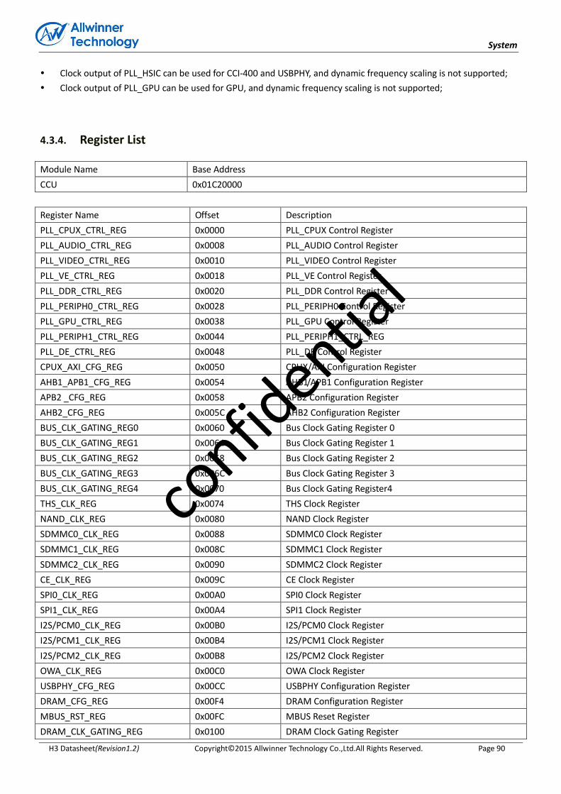
System
H3 Datasheet(Revision1.2) Copyright© 2015 Allwinner Technology Co.,Ltd.All Rights Reserved. Page 90
Clock output of PLL_HSIC can be used for CCI-400 and USBPHY, and dynamic frequency scaling is not supported;
Clock output of PLL_GPU can be used for GPU, and dynamic frequency scaling is not supported;
4.3.4. Register List
Module Name Base Address
CCU 0x01C20000
Register Name Offset Description
PLL_CPUX_CTRL_REG 0x0000 PLL_CPUX Control Register
PLL_AUDIO_CTRL_REG 0x0008 PLL_AUDIO Control Register
PLL_VIDEO_CTRL_REG 0x0010 PLL_VIDEO Control Register
PLL_VE_CTRL_REG 0x0018 PLL_VE Control Register
PLL_DDR_CTRL_REG 0x0020 PLL_DDR Control Register
PLL_PERIPH0_CTRL_REG 0x0028 PLL_PERIPH0 Control Register
PLL_GPU_CTRL_REG 0x0038 PLL_GPU Control Register
PLL_PERIPH1_CTRL_REG 0x0044 PLL_PERIPH1_CTRL_REG
PLL_DE_CTRL_REG 0x0048 PLL_DE Control Register
CPUX_AXI_CFG_REG 0x0050 CPUX/AXI Configuration Register
AHB1_APB1_CFG_REG 0x0054 AHB1/APB1 Configuration Register
APB2 _CFG_REG 0x0058 APB2 Configuration Register
AHB2_CFG_REG 0x005C AHB2 Configuration Register
BUS_CLK_GATING_REG0 0x0060 Bus Clock Gating Register 0
BUS_CLK_GATING_REG1 0x0064 Bus Clock Gating Register 1
BUS_CLK_GATING_REG2 0x0068 Bus Clock Gating Register 2
BUS_CLK_GATING_REG3 0x006C Bus Clock Gating Register 3
BUS_CLK_GATING_REG4 0x0070 Bus Clock Gating Register4
THS_CLK_REG 0x0074 THS Clock Register
NAND_CLK_REG 0x0080 NAND Clock Register
SDMMC0_CLK_REG 0x0088 SDMMC0 Clock Register
SDMMC1_CLK_REG 0x008C SDMMC1 Clock Register
SDMMC2_CLK_REG 0x0090 SDMMC2 Clock Register
CE_CLK_REG 0x009C CE Clock Register
SPI0_CLK_REG 0x00A0 SPI0 Clock Register
SPI1_CLK_REG 0x00A4 SPI1 Clock Register
I2S/PCM0_CLK_REG 0x00B0 I2S/PCM0 Clock Register
I2S/PCM1_CLK_REG 0x00B4 I2S/PCM1 Clock Register
I2S/PCM2_CLK_REG 0x00B8 I2S/PCM2 Clock Register
OWA_CLK_REG 0x00C0 OWA Clock Register
USBPHY_CFG_REG 0x00CC USBPHY Configuration Register
DRAM_CFG_REG 0x00F4 DRAM Configuration Register
MBUS_RST_REG 0x00FC MBUS Reset Register
DRAM_CLK_GATING_REG 0x0100 DRAM Clock Gating Register
confid
ential

System
H3 Datasheet(Revision1.2) Copyright© 2015 Allwinner Technology Co.,Ltd.All Rights Reserved. Page 91
TCON0_CLK_REG 0x0118 TCON0 Clock Register
TVE_CLK_REG 0x0120 TVE Clock Register
DEINTERLACE_CLK_REG 0x0124 DEINTERLACE Clock Register
CSI_MISC_CLK_REG 0x0130 CSI_MISC Clock Register
CSI_CLK_REG 0x0134 CSI Clock Register
VE_CLK_REG 0x013C VE Clock Register
AC_DIG_CLK_REG 0x0140 AC Digital Clock Register
AVS_CLK_REG 0x0144 AVS Clock Register
HDMI_CLK_REG 0x0150 HDMI Clock Register
HDMI_SLOW_CLK_REG 0x0154 HDMI Slow Clock Register
MBUS_CLK_REG 0x015C MBUS Clock Register
GPU_CLK_REG 0x01A0 GPU Clock Register
PLL_STABLE_TIME_REG0 0x0200 PLL Stable Time Register 0
PLL_STABLE_TIME_REG1 0x0204 PLL Stable Time Register 1
PLL_CPUX_BIAS_REG 0x0220 PLL_CPUX Bias Register
PLL_AUDIO_BIAS_REG 0x0224 PLL_AUDIO Bias Register
PLL_VIDEO_BIAS_REG 0x0228 PLL_VIDEO Bias Register
PLL_VE_BIAS_REG 0x022C PLL_VE Bias Register
PLL_DDR_BIAS_REG 0x0230 PLL_DDR Bias Register
PLL_PERIPH0_BIAS_REG 0x0234 PLL_PERIPH0 Bias Register
PLL_GPU_BIAS_REG 0x023C PLL_GPU Bias Register
PLL_PERIPH1_BIAS_REG 0x0244 PLL_PERIPH1 Bias Register
PLL_DE_BIAS_REG 0x0248 PLL_DE Bias Register
PLL_CPUX_TUN_REG 0x0250 PLL_CPUX Tuning Register
PLL_DDR_TUN_REG 0x0260 PLL_DDR Tuning Register
PLL_CPUX_PAT_CTRL_REG 0x0280 PLL_CPUX Pattern Control Register
PLL_AUDIO_PAT_CTRL_REG0 0x0284 PLL_AUDIO Pattern Control Register
PLL_VIDEO_PAT_CTRL_REG0 0x0288 PLL_VIDEO Pattern Control Register
PLL_VE_PAT_CTRL_REG 0x028C PLL_VE Pattern Control Register
PLL_DDR_PAT_CTRL_REG0 0x0290 PLL_DDR Pattern Control Register
PLL_GPU_PAT_CTRL_REG 0x029C PLL_GPU Pattern Control Register
PLL_PERIPH1_PAT_CTRL_REG1 0x02A4 PLL_PERIPH1 Pattern Control Register
PLL_DE_PAT_CTRL_REG 0x02A8 PLL_DE Pattern Control Register
BUS_SOFT_RST_REG0 0x02C0 Bus Software Reset Register 0
BUS_SOFT_RST_REG1 0x02C4 Bus Software Reset Register 1
BUS_SOFT_RST_REG2 0x02C8 Bus Software Reset Register 2
BUS_SOFT_RST_REG3 0x02D0 Bus Software Reset Register 3
BUS_SOFT_RST_REG4 0x02D8 Bus Software Reset Register 4
CCU_SEC_SWITCH_REG 0x02F0 CCU Security Switch Register
PS_CTRL_REG 0x0300 PS Control Register
PS_CNT_REG 0x0304 PS Counter Register
confid
ential

System
H3 Datasheet(Revision1.2) Copyright© 2015 Allwinner Technology Co.,Ltd.All Rights Reserved. Page 92
4.3.5. Register Description
4.3.5.1. PLL_CPUX Control Register (Default Value: 0x00001000)
Offset: 0x0000 Register Name: PLL_CPUX_CTRL_REG
Bit R/W Default/Hex Description
31 R/W 0x0 PLL_ENABLE.
0: Disable
1: Enable
The PLL Output= (24MHz*N*K)/(M*P).
The PLL output is for the CPUX Clock.
Note: The PLL output clock must be in the range of 200MHz~2.6GHz.
Its default is 408MHz.
30:29 / / /
28 R 0x0 LOCK
0: Unlocked
1: Locked (It indicates that the PLL has been stable.)
27:25 / / /
24 R/W 0x0 CPUX_SDM_EN.
0: Disable
1: Enable
23:18 / / /
17:16 R/W 0x0 PLL_OUT_EXT_DIVP
PLL Output external divider P
00: /1
01: /2
10: /4
11: /
Note:The P factor only use in the condition that PLL output less than 288
MHz.
15:13 / / /
12:8 R/W 0x10 PLL_FACTOR_N
PLL Factor N.
Factor=0, N=1
Factor=1, N=2
Factor=2, N=3
……
Factor=31, N=32
7:6 / / /
5:4 R/W 0x0 PLL_FACTOR_K.
PLL Factor K.(K=Factor + 1 )
The range is from 1 to 4.
3:2 / / /
1:0 R/W 0x0 PLL_FACTOR_M.
confid
ential
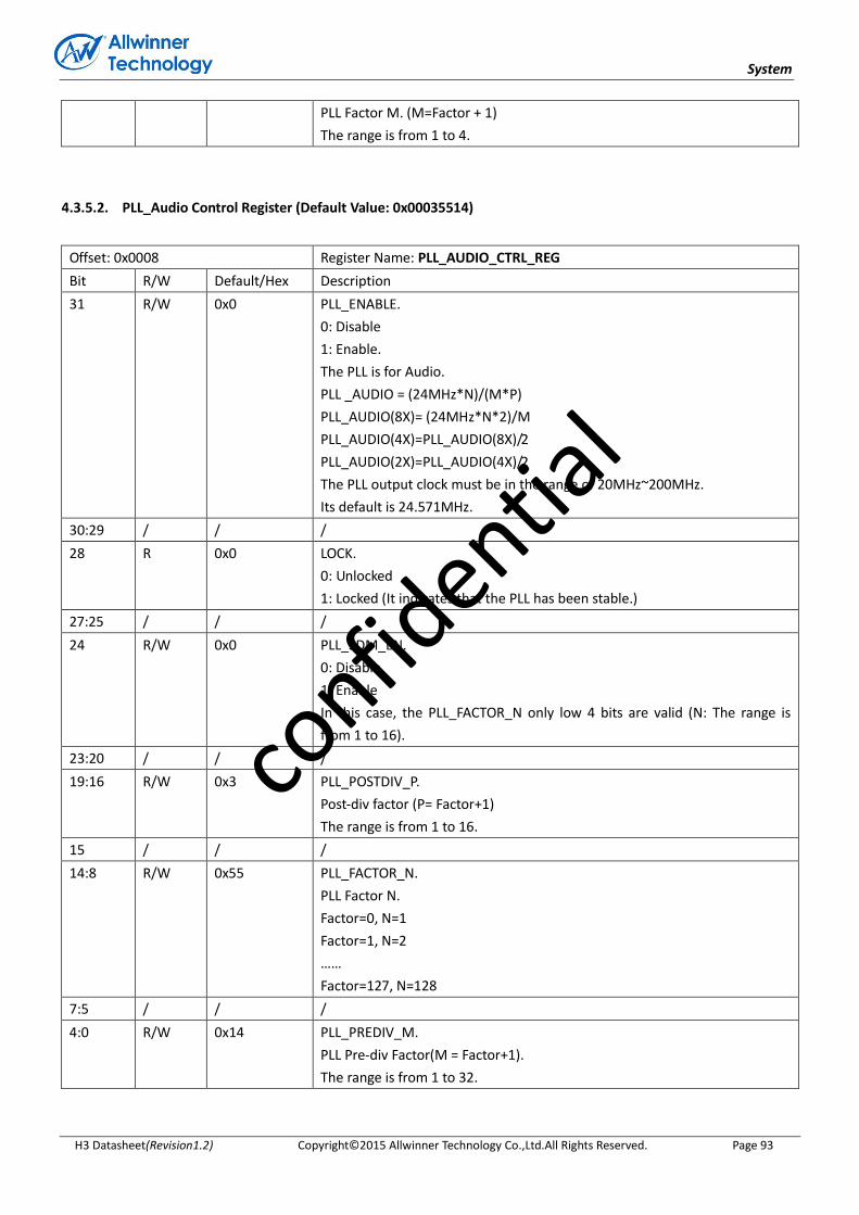
System
H3 Datasheet(Revision1.2) Copyright© 2015 Allwinner Technology Co.,Ltd.All Rights Reserved. Page 93
PLL Factor M. (M=Factor + 1)
The range is from 1 to 4.
4.3.5.2. PLL_Audio Control Register (Default Value: 0x00035514)
Offset: 0x0008 Register Name: PLL_AUDIO_CTRL_REG
Bit R/W Default/Hex Description
31 R/W 0x0 PLL_ENABLE.
0: Disable
1: Enable.
The PLL is for Audio.
PLL _AUDIO = (24MHz*N)/(M*P)
PLL_AUDIO(8X)= (24MHz*N*2)/M
PLL_AUDIO(4X)=PLL_AUDIO(8X)/2
PLL_AUDIO(2X)=PLL_AUDIO(4X)/2
The PLL output clock must be in the range of 20MHz~200MHz.
Its default is 24.571MHz.
30:29 / / /
28 R 0x0 LOCK.
0: Unlocked
1: Locked (It indicates that the PLL has been stable.)
27:25 / / /
24 R/W 0x0 PLL_SDM_EN.
0: Disable
1: Enable
In this case, the PLL_FACTOR_N only low 4 bits are valid (N: The range is
from 1 to 16).
23:20 / / /
19:16 R/W 0x3 PLL_POSTDIV_P.
Post-div factor (P= Factor+1)
The range is from 1 to 16.
15 / / /
14:8 R/W 0x55 PLL_FACTOR_N.
PLL Factor N.
Factor=0, N=1
Factor=1, N=2
……
Factor=127, N=128
7:5 / / /
4:0 R/W 0x14 PLL_PREDIV_M.
PLL Pre-div Factor(M = Factor+1).
The range is from 1 to 32.
confid
ential
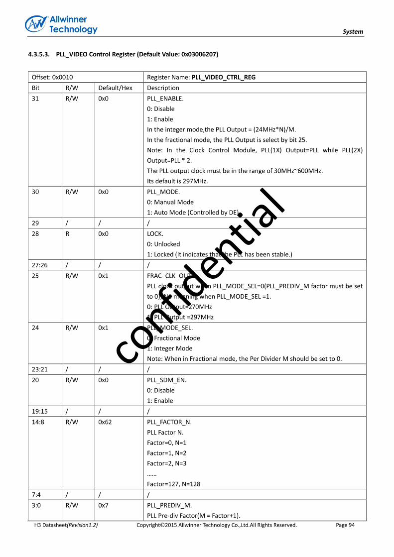
System
H3 Datasheet(Revision1.2) Copyright© 2015 Allwinner Technology Co.,Ltd.All Rights Reserved. Page 94
4.3.5.3. PLL_VIDEO Control Register (Default Value: 0x03006207)
Offset: 0x0010 Register Name: PLL_VIDEO_CTRL_REG
Bit R/W Default/Hex Description
31 R/W 0x0 PLL_ENABLE.
0: Disable
1: Enable
In the integer mode,the PLL Output = (24MHz*N)/M.
In the fractional mode, the PLL Output is select by bit 25.
Note: In the Clock Control Module, PLL(1X) Output=PLL while PLL(2X)
Output=PLL * 2.
The PLL output clock must be in the range of 30MHz~600MHz.
Its default is 297MHz.
30 R/W 0x0 PLL_MODE.
0: Manual Mode
1: Auto Mode (Controlled by DE)
29 / / /
28 R 0x0 LOCK.
0: Unlocked
1: Locked (It indicates that the PLL has been stable.)
27:26 / / /
25 R/W 0x1 FRAC_CLK_OUT.
PLL clock output when PLL_MODE_SEL=0(PLL_PREDIV_M factor must be set
to 0); No meaning when PLL_MODE_SEL =1.
0: PLL Output=270MHz
1: PLL Output =297MHz
24 R/W 0x1 PLL_MODE_SEL.
0: Fractional Mode
1: Integer Mode
Note: When in Fractional mode, the Per Divider M should be set to 0.
23:21 / / /
20 R/W 0x0 PLL_SDM_EN.
0: Disable
1: Enable
19:15 / / /
14:8 R/W 0x62 PLL_FACTOR_N.
PLL Factor N.
Factor=0, N=1
Factor=1, N=2
Factor=2, N=3
……
Factor=127, N=128
7:4 / / /
3:0 R/W 0x7 PLL_PREDIV_M.
PLL Pre-div Factor(M = Factor+1).
confid
ential

System
H3 Datasheet(Revision1.2) Copyright© 2015 Allwinner Technology Co.,Ltd.All Rights Reserved. Page 95
The range is from 1 to 16.
4.3.5.4. PLL_VE Control Register (Default Value: 0x03006207)
Offset: 0x0018 Register Name: PLL_VE_CTRL_REG
Bit R/W Default/Hex Description
31 R/W 0x0 PLL_ENABLE.
0: Disable
1: Enable
In the integer mode, The PLL Output = (24MHz*N)/M.
In the fractional mode, the PLL Output is select by bit 25.
Note: The PLL output clock must be in the range of 30MHz~600MHz.
Its default is 297MHz.
30:29 / / /
28 R 0x0 LOCK
0: Unlocked
1: Locked (It indicates that the PLL has been stable.)
27:26 / / /
25 R/W 0x1 FRAC_CLK_OUT.
PLL clock output when PLL_MODE_SEL=0(PLL_PREDIV_M factor must be set
to 0); No meaning when PLL_MODE_SEL =1.
0: PLL Output=270MHz
1: PLL Output =297MHz
24 R/W 0x1 PLL_MODE_SEL.
0: Fractional Mode
1: Integer Mode
Note: When in Fractional mode, the Per Divider M should be set to 0.
23:21 / / /
20 R/W 0x0 PLL_SDM_EN.
0: Disable
1: Enable
19:15 / / /
14:8 R/W 0x62 PLL_FACTOR_N.
PLL Factor N.
Factor=0, N=1
Factor=1, N=2
Factor=2, N=3
……
Factor=31, N=32
…
Factor=127, N=128
7:4 / / /
3:0 R/W 0x7 PLL_PREDIV_M.
PLL Pre Divider (M = Factor+1).
confid
ential

System
H3 Datasheet(Revision1.2) Copyright© 2015 Allwinner Technology Co.,Ltd.All Rights Reserved. Page 96
The range is from 1 to 16.
4.3.5.5. PLL_DDR Control Register (Default Value: 0x00001000)
Offset: 0x0020 Register Name: PLL_DDR_CTRL_REG
Bit R/W Default/Hex Description
31 R/W 0x0 PLL_ENABLE.
0: Disable
1: Enable
Set bit20 to validate the PLL after this bit is set to 1.
The PLL Output = (24MHz*N*K)/M.
Note: the PLL output clock must be in the range of 200MHz~2.6GHz.
Its default is 408MHz.
30:29 / / /
28 R 0x0 LOCK
0: Unlocked
1: Locked (It indicates that the PLL has been stable.)
27:25 / / /
24 R/W 0x0 PLL_SDM_EN.
0: Disable
1: Enable
23:21 / / /
20 R/W 0x0 PLL_DDR_CFG_UPDATE.
PLL_DDR Configuration Update.
When PLL_DDR has been changed, this bit should be set to 1 to validate the
PLL, otherwise the change would be invalid. And this bit would be cleared
automatically after the PLL change is valid.
0: No effect
1: Validating the PLL_DDR
19:13 / / /
12:8 R/W 0x10 PLL_FACTOR_N.
PLL Factor N.
Factor=0, N=1
Factor=1, N=2
Factor=2, N=3
……
Factor=31, N=32
7:6 / / /
5:4 R/W 0x0 PLL_FACTOR_K.
PLL Factor K.(K=Factor + 1 )
The range is from 1 to 4.
3:2 / / /
1:0 R/W 0x0 PLL_FACTOR_M.
PLL Factor M.(M = Factor + 1 )
confid
ential

System
H3 Datasheet(Revision1.2) Copyright© 2015 Allwinner Technology Co.,Ltd.All Rights Reserved. Page 97
The range is from 1 to 4.
4.3.5.6. PLL_PERIPH0 Control Register (Default Value: 0x00041811)
Offset: 0x0028 Register Name: PLL_PERIPH0_CTRL_REG
Bit R/W Default/Hex Description
31 R/W 0x0 PLL_ENABLE.
0: Disable
1: Enable
The PLL Output = 24MHz*N*K/2.
Note: The PLL Output should be fixed to 600MHz, it is not recommended to
vary this value arbitrarily.
In the Clock Control Module, PLL(2X) output= PLL*2 = 24MHz*N*K.
The PLL output clock must be in the range of 200MHz~1.8GHz.
Its default is 600MHz.
30:29 / / /
28 R 0x0 LOCK.
0: Unlocked
1: Locked (It indicates that the PLL has been stable.)
27:26 / / /
25 R/W 0x0 PLL_BYPASS_EN.
PLL Output Bypass Enable.
0: Disable
1: Enable
If the bypass is enabled, the PLL output is 24MHz.
24 R/W 0x0 PLL_CLK_OUT_EN.
PLL clock output enable.
0: Disable
1: Enable
23:19 / / /
18 R/W 0x1 PLL_24M_OUT_EN.
PLL 24MHz Output Enable.
0: Disable
1: Enable
When 25MHz crystal used, this PLL can output 24MHz.
17:16 R/W 0x0 PLL_24M_POST_DIV.
PLL 24M Output Clock Post Divider (When 25MHz crystal used).
1/2/3/4.
15:13 / / /
12:8 R/W 0x18 PLL_FACTOR_N.
PLL Factor N.
Factor=0, N=1
Factor=1, N=2
Factor=2, N=3
confid
ential
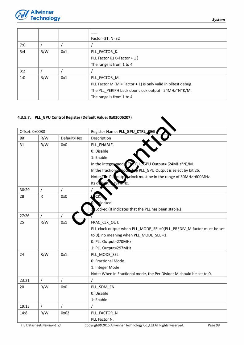
System
H3 Datasheet(Revision1.2) Copyright© 2015 Allwinner Technology Co.,Ltd.All Rights Reserved. Page 98
……
Factor=31, N=32
7:6 / / /
5:4 R/W 0x1 PLL_FACTOR_K.
PLL Factor K.(K=Factor + 1 )
The range is from 1 to 4.
3:2 / / /
1:0 R/W 0x1 PLL_FACTOR_M.
PLL Factor M (M = Factor + 1) is only valid in plltest debug.
The PLL_PERIPH back door clock output =24MHz*N*K/M.
The range is from 1 to 4.
4.3.5.7. PLL_GPU Control Register (Default Value: 0x03006207)
Offset: 0x0038 Register Name: PLL_GPU_CTRL_REG
Bit R/W Default/Hex Description
31 R/W 0x0 PLL_ENABLE.
0: Disable
1: Enable
In the integer mode, The PLL_GPU Output= (24MHz*N)/M.
In the fractional mode, the PLL_GPU Output is select by bit 25.
Note: The PLL output clock must be in the range of 30MHz~600MHz.
Its default is 297MHz.
30:29 / / /
28 R 0x0 LOCK.
0: Unlocked
1: Locked (It indicates that the PLL has been stable.)
27:26 / / /
25 R/W 0x1 FRAC_CLK_OUT.
PLL clock output when PLL_MODE_SEL=0(PLL_PREDIV_M factor must be set
to 0); no meaning when PLL_MODE_SEL =1.
0: PLL Output=270MHz
1: PLL Output=297MHz
24 R/W 0x1 PLL_MODE_SEL.
0: Fractional Mode.
1: Integer Mode
Note: When in Fractional mode, the Per Divider M should be set to 0.
23:21 / / /
20 R/W 0x0 PLL_SDM_EN.
0: Disable
1: Enable
19:15 / / /
14:8 R/W 0x62 PLL_FACTOR_N
PLL Factor N.
confid
ential

System
H3 Datasheet(Revision1.2) Copyright© 2015 Allwinner Technology Co.,Ltd.All Rights Reserved. Page 99
Factor=0, N=1
Factor=1, N=2
Factor=2, N=3
……
Factor=127, N=128
7:4 / / /
3:0 R/W 0x7 PLL_PRE_DIV_M.
PLL Pre Divider (M = Factor+1).
The range is from 1 to 16.
4.3.5.8. PLL_PERIPH1 Control Register (Default Value: 0x00041811)
Offset: 0x0044 Register Name: PLL_PERIPH1_CTRL_REG
Bit R/W Default/Hex Description
31 R/W 0x0 PLL_ENABLE.
0: Disable
1: Enable
The PLL Output = 24MHz*N*K/2.
Note: The PLL Output should be fixed to 600MHz, it is not recommended to
vary this value arbitrarily.
In the Clock Control Module, PLL(2X) output= PLL*2 = 24MHz*N*K.
The PLL output clock must be in the range of 200MHz~1.8GHz.
Its default is 600MHz.
30:29 / / /
28 R 0x0 LOCK.
0: Unlocked
1: Locked (It indicates that the PLL has been stable.)
27:26 / / /
25 R/W 0x0 PLL_BYPASS_EN.
PLL Output Bypass Enable.
0: Disable
1: Enable
If the bypass is enabled, the PLL output is 24MHz.
24 R/W 0x0 PLL_CLK_OUT_EN.
PLL clock output enable.
0: Disable
1: Enable
23:21 / / /
20 R/W 0x0 PLL_SDM_EN.
0: Disable
1: Enable
19 / / /
18 R/W 0x1 PLL_24M_OUT_EN.
PLL 24MHz Output Enable.
confid
ential
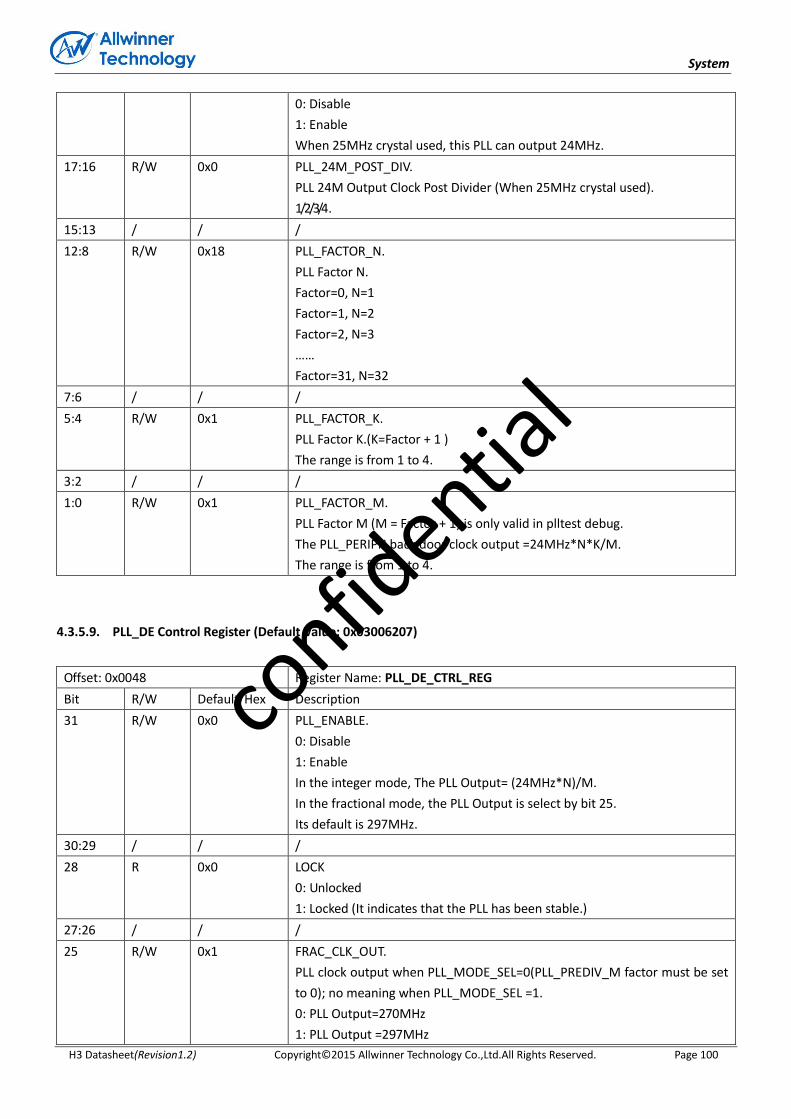
System
H3 Datasheet(Revision1.2) Copyright© 2015 Allwinner Technology Co.,Ltd.All Rights Reserved. Page 100
0: Disable
1: Enable
When 25MHz crystal used, this PLL can output 24MHz.
17:16 R/W 0x0 PLL_24M_POST_DIV.
PLL 24M Output Clock Post Divider (When 25MHz crystal used).
1/2/3/4.
15:13 / / /
12:8 R/W 0x18 PLL_FACTOR_N.
PLL Factor N.
Factor=0, N=1
Factor=1, N=2
Factor=2, N=3
……
Factor=31, N=32
7:6 / / /
5:4 R/W 0x1 PLL_FACTOR_K.
PLL Factor K.(K=Factor + 1 )
The range is from 1 to 4.
3:2 / / /
1:0 R/W 0x1 PLL_FACTOR_M.
PLL Factor M (M = Factor + 1) is only valid in plltest debug.
The PLL_PERIPH back door clock output =24MHz*N*K/M.
The range is from 1 to 4.
4.3.5.9. PLL_DE Control Register (Default Value: 0x03006207)
Offset: 0x0048 Register Name: PLL_DE_CTRL_REG
Bit R/W Default/Hex Description
31 R/W 0x0 PLL_ENABLE.
0: Disable
1: Enable
In the integer mode, The PLL Output= (24MHz*N)/M.
In the fractional mode, the PLL Output is select by bit 25.
Its default is 297MHz.
30:29 / / /
28 R 0x0 LOCK
0: Unlocked
1: Locked (It indicates that the PLL has been stable.)
27:26 / / /
25 R/W 0x1 FRAC_CLK_OUT.
PLL clock output when PLL_MODE_SEL=0(PLL_PREDIV_M factor must be set
to 0); no meaning when PLL_MODE_SEL =1.
0: PLL Output=270MHz
1: PLL Output =297MHz
confid
ential
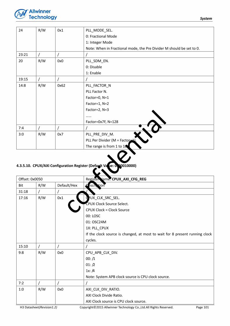
System
H3 Datasheet(Revision1.2) Copyright© 2015 Allwinner Technology Co.,Ltd.All Rights Reserved. Page 101
24 R/W 0x1 PLL_MODE_SEL.
0: Fractional Mode
1: Integer Mode
Note: When in Fractional mode, the Pre Divider M should be set to 0.
23:21 / / /
20 R/W 0x0 PLL_SDM_EN.
0: Disable
1: Enable
19:15 / / /
14:8 R/W 0x62 PLL_FACTOR_N
PLL Factor N.
Factor=0, N=1
Factor=1, N=2
Factor=2, N=3
……
Factor=0x7F, N=128
7:4 / / /
3:0 R/W 0x7 PLL_PRE_DIV_M.
PLL Per Divider (M = Factor+1).
The range is from 1 to 16.
4.3.5.10. CPUX/AXI Configuration Register (Default Value: 0x00010000)
Offset: 0x0050 Register Name: CPUX_AXI_CFG_REG
Bit R/W Default/Hex Description
31:18 / / /
17:16 R/W 0x1 CPUX_CLK_SRC_SEL.
CPUX Clock Source Select.
CPUX Clock = Clock Source
00: LOSC
01: OSC24M
1X: PLL_CPUX
If the clock source is changed, at most to wait for 8 present running clock
cycles.
15:10 / / /
9:8 R/W 0x0 CPU_APB_CLK_DIV.
00: /1
01: /2
1x: /4
Note: System APB clock source is CPU clock source.
7:2 / / /
1:0 R/W 0x0 AXI_CLK_DIV_RATIO.
AXI Clock Divide Ratio.
AXI Clock source is CPU clock source.
confid
ential

System
H3 Datasheet(Revision1.2) Copyright© 2015 Allwinner Technology Co.,Ltd.All Rights Reserved. Page 102
00: /1
01: /2
10: /3
11: /4
4.3.5.11. AHB1/APB1 Configuration Register (Default Value: 0x00001010)
Offset: 0x0054 Register Name: AHB1_APB1_CFG_REG
Bit R/W Default/Hex Description
31:14 / / /
13:12 R/W 0x1 AHB1_CLK_SRC_SEL.
00: LOSC
01: OSC24M
10: AXI
11: PLL_PERIPH0/ AHB1_PRE_DIV
11:10 / / /
9:8 R/W 0x0 APB1_CLK_RATIO.
APB1 Clock Divide Ratio. APB1 clock source is AHB1 clock.
00: /2
01: /2
10: /4
11: /8
7:6 R/W 0x0 AHB1_PRE_DIV
AHB1 Clock Pre Divide Ratio
00: /1
01: /2
10: /3
11: /4
5:4 R/W 0x1 AHB1_CLK_DIV_RATIO.
AHB1 Clock Divide Ratio.
00: /1
01: /2
10: /4
11: /8
3:0 / / /
4.3.5.12. APB2 Configuration Register (Default Value: 0x01000000)
Offset: 0x0058 Register Name: APB2_CFG_REG
Bit R/W Default/Hex Description
31:26 / / /
25:24 R/W 0x1 APB2_CLK_SRC_SEL.
confid
ential
System
H3 Datasheet(Revision1.2) Copyright© 2015 Allwinner Technology Co.,Ltd.All Rights Reserved. Page 103
APB2 Clock Source Select
00: LOSC
01: OSC24M
1X: PLL_PERIPH0
This clock is used for some special module apbclk(UART、TWI). Because
these modules need special clock rate even if the apb1clk changed.
23:18 / / /
17:16 R/W 0x0 CLK_RAT_N
Clock Pre Divide Ratio (n)
The select clock source is pre-divided by 2^n. The divider is 1/2/4/8.
15:5 / / /
4:0 R/W 0x0 CLK_RAT_M.
Clock Divide Ratio (m)
The Pre Divide clock is divided by (m+1). The divider M is from 1 to 32.
4.3.5.13. AHB2 Configuration Register (Default Value: 0x00000000)
Offset: 0x005C Register Name: AHB2_CFG_REG
Bit R/W Default/Hex Description
31:2 / / /
1:0 R/W 0x0 AHB2_CLK_CFG.
00: AHB1 Clock
01: PLL_PERIPH0 / 2
1X: /
EMAC ,USBHCI1/2/3 default clock source is AHB2 Clock.
4.3.5.14. Bus Clock Gating Register0 (Default Value: 0x00000000)
Offset: 0x0060 Register Name: BUS_CLK_GATING_REG0
Bit R/W Default/Hex Description
31 R/W 0x0 USBOHCI3_GATING.
Gating Clock for USB OHCI3
0: Mask
1: Pass
30 R/W 0x0 USBOHCI2_GATING.
Gating Clock for USB OHCI2
0: Mask
1: Pass
29 R/W 0x0 USBOHCI1_GATING.
Gating Clock for USB OHCI1
0: Mask
1: Pass
confid
ential

System
H3 Datasheet(Revision1.2) Copyright© 2015 Allwinner Technology Co.,Ltd.All Rights Reserved. Page 104
28 R/W 0x0 USB OTG_OHCI0_GATING.
Gating Clock for USB OTG_OHCI0
0: Mask
1: Pass
27 R/W 0x0 USBEHCI3_GATING.
Gating Clock For USB EHCI3
0: Mask
1: Pass
26 R/W 0x0 USBEHCI2_GATING.
Gating Clock For USB EHCI2
0: Mask
1: Pass
25 R/W 0x0 USBEHCI1_GATING.
Gating Clock For USB EHCI1
0: Mask
1: Pass
24 R/W 0x0 USB OTG_EHCI0_GATING.
Gating Clock For USB OTG_EHCI0
0: Mask
1: Pass
23 R/W 0x0 USB OTG_Device_GATING.
Gating Clock For USB OTG_Device
0: Mask
1: Pass
22 / / /
21 R/W 0x0 SPI1_GATING.
Gating Clock For SPI1
0: Mask
1: Pass
20 R/W 0x0 SPI0_GATING.
Gating Clock For SPI0
0: Mask
1: Pass
19 R/W 0x0 HSTMR_GATING.
Gating Clock For High Speed Timer
0: Mask
1: Pass
18 R/W 0x0 TS_GATING.
Gating Clock For TS
0: Mask
1: Pass
17 R/W 0x0 EMAC_GATING.
Gating Clock For EMAC
0: Mask
1: Pass
confid
ential
System
H3 Datasheet(Revision1.2) Copyright© 2015 Allwinner Technology Co.,Ltd.All Rights Reserved. Page 105
16:15 / / /
14 R/W 0x0 DRAM_GATING.
Gating Clock For DRAM
0: Mask
1: Pass
13 R/W 0x0 NAND_GATING.
Gating Clock For NAND
0: Mask
1: Pass
12:11 / / /
10 R/W 0x0 MMC2_GATING.
Gating Clock For MMC2
0: Mask
1: Pass
9 R/W 0x0 MMC1_GATING.
Gating Clock For MMC1
0: Mask
1: Pass
8 R/W 0x0 MMC0_GATING.
Gating Clock For MMC0
0: Mask
1: Pass
7 / / /
6 R/W 0x0 DMA_GATING.
Gating Clock For DMA
0: Mask
1: Pass
5 R/W 0x0 CE_GATING.
Gating Clock For CE.
0: Mask
1: Pass
4:0 / / /
4.3.5.15. Bus Clock Gating Register1 (Default Value: 0x00000000)
Offset: 0x0064 Register Name: BUS_CLK_GATING_REG1
Bit R/W Default/Hex Description
31:23 / / /
22 R/W 0x0 SPINLOCK_GATING.
0: Mask
1: Pass.
21 R/W 0x0 MSGBOX_GATING.
0: Mask
1: Pass.
confid
ential
System
H3 Datasheet(Revision1.2) Copyright© 2015 Allwinner Technology Co.,Ltd.All Rights Reserved. Page 106
20 R/W 0x0 GPU_GATING.
0: Mask
1: Pass.
19:13 / / /
12 R/W 0x0 DE_GATING.
0: Mask
1: Pass.
11 R/W 0x0 HDMI_GATING.
0: Mask
1: Pass.
10 / / /
9 R/W 0x0 TVE_GATING.
Gating Clock For TVE
0: Mask
1: Pass.
8 R/W 0x0 CSI_GATING.
0: Mask
1: Pass.
7:6 / / /
5 R/W 0x0 DEINTERLACE_GATING.
Gating Clock For DEINTERLACE
0: Mask
1: Pass
4 R/W 0x0 TCON1_GATING.
Gating Clock For TCON1
0: Mask
1: Pass.
3 R/W 0x0 TCON0_GATING.
Gating Clock For TCON0
0: Mask
1: Pass.
2:1 / / /
0 R/W 0x0 VE_GATING.
Gating Clock For VE
0: Mask
1: Pass.
4.3.5.16. Bus Clock Gating Register2 (Default Value: 0x00000000)
Offset: 0x0068 Register Name: BUS_CLK_GATING_REG2
Bit R/W Default/Hex Description
31:15 / / /
14 R/W 0x0 I2S/PCM 2_GATING.
Gating Clock For I2S/PCM 2
confid
ential
System
H3 Datasheet(Revision1.2) Copyright© 2015 Allwinner Technology Co.,Ltd.All Rights Reserved. Page 107
0: Mask
1: Pass.
13 R/W 0x0 I2S/PCM 1_GATING.
Gating Clock For I2S/PCM 1
0: Mask
1: Pass.
12 R/W 0x0 I2S/PCM 0_GATING.
Gating Clock For I2S/PCM 0
0: Mask
1: Pass.
11:9 / / /
8 R/W 0x0 THS_GATING.
Gating Clock For THS
0: Mask
1: Pass
7:6 / / /
5 R/W 0x0 PIO_GATING.
Gating Clock For PIO
0: Mask
1: Pass.
4:2 / / /
1 R/W 0x0 OWA_GATING.
Gating Clock For OWA
0: Mask
1: Pass.
0 R/W 0x0 AC_DIG_GATING.
Gating Clock For AC Digital
0: Mask
1: Pass
4.3.5.17. Bus Clock Gating Register3 (Default Value: 0x00000000)
Offset: 0x006C Register Name: BUS_CLK_GATING_REG3
Bit R/W Default/Hex Description
31:21 / / /
20 R/W 0x0 SCR_GATING.
Gating Clock For SCR
0: Mask
1: Pass
19 R/W 0x0 UART3_GATING.
Gating Clock For UART3
0: Mask
1: Pass.
18 R/W 0x0 UART2_GATING.
confid
ential

System
H3 Datasheet(Revision1.2) Copyright© 2015 Allwinner Technology Co.,Ltd.All Rights Reserved. Page 108
Gating Clock For UART2
0: Mask
1: Pass.
17 R/W 0x0 UART1_GATING.
Gating Clock For UART1
0: Mask
1: Pass.
16 R/W 0x0 UART0_GATING.
Gating Clock For UART0
0: Mask
1: Pass.
15:3 / / /
2 R/W 0x0 TWI2_GATING.
Gating Clock For TWI2
0: Mask
1: Pass.
1 R/W 0x0 TWI1_GATING.
Gating Clock For TWI1
0: Mask
1: Pass.
0 R/W 0x0 TWI0_GATING.
Gating Clock For TWI0
0: Mask
1: Pass.
4.3.5.18. Bus Clock Gating Register4 (Default Value: 0x00000000)
Offset: 0x0070 Register Name: BUS_CLK_GATING_REG4
Bit R/W Default/Hex Description
31:8 / / /
7 R/W 0x0 DBGSYS_GATING.
Gating Clock For DBGSYS
0: Mask
1: Pass
6:1 / / /
0 R/W 0x0 EPHY_GATING.
Gating Clock For EPHY
0: Mask
1: Pass
confid
ential

System
H3 Datasheet(Revision1.2) Copyright© 2015 Allwinner Technology Co.,Ltd.All Rights Reserved. Page 109
4.3.5.19. THS Clock Register (Default Value: 0x00000000)
Offset: 0x0074 Register Name: THS_CLK_REG
Bit R/W Default/Hex Description
31 R/W 0x0 SCLK_GATING.
Gating Special Clock.
0: Clock is OFF
1: Clock is ON
This special clock = Clock Source/CLK_DIV_RATIO.
30:26 / / /
25:24 R/W 0x0 THS_CLK_SRC_SEL.
Clock Source Select
00: OSC24M
01: /
10: /
11: /
23:2 / / /
1:0 R/W 0x0 THS_CLK_DIV_RATIO.
THS clock divide ratio.
00: /1
01: /2
10: /4
11: /6
4.3.5.20. NAND Clock Register (Default Value: 0x00000000)
Offset: 0x0080 Register Name: NAND_CLK_REG
Bit R/W Default/Hex Description
31 R/W 0x0 SCLK_GATING.
Gating Special Clock(Max Clock = 200MHz)
0: Clock is OFF
1: Clock is ON.
SCLK = Clock Source/Divider N/Divider M.
30:26 / / /
25:24 R/W 0x0 CLK_SRC_SEL.
Clock Source Select
00: OSC24M
01: PLL_PERIPH0
10: PLL_PERIPH1
11: /
23:18 / / /
17:16 R/W 0x0 CLK_DIV_RATIO_N.
Clock Pre Divide Ratio (n)
confid
ential
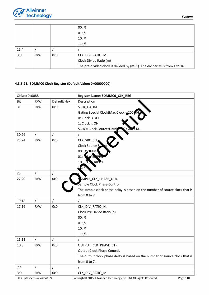
System
H3 Datasheet(Revision1.2) Copyright© 2015 Allwinner Technology Co.,Ltd.All Rights Reserved. Page 110
00: /1
01: /2
10: /4
11: /8.
15:4 / / /
3:0 R/W 0x0 CLK_DIV_RATIO_M
Clock Divide Ratio (m)
The pre-divided clock is divided by (m+1). The divider M is from 1 to 16.
4.3.5.21. SDMMC0 Clock Register (Default Value: 0x00000000)
Offset: 0x0088 Register Name: SDMMC0_CLK_REG
Bit R/W Default/Hex Description
31 R/W 0x0 SCLK_GATING.
Gating Special Clock(Max Clock = 200MHz)
0: Clock is OFF
1: Clock is ON.
SCLK = Clock Source/Divider N/Divider M.
30:26 / / /
25:24 R/W 0x0 CLK_SRC_SEL.
Clock Source Select
00: OSC24M
01: PLL_PERIPH0
10: PLL_PERIPH1
11: /
23 / / /
22:20 R/W 0x0 SAMPLE_CLK_PHASE_CTR.
Sample Clock Phase Control.
The sample clock phase delay is based on the number of source clock that is
from 0 to 7.
19:18 / / /
17:16 R/W 0x0 CLK_DIV_RATIO_N.
Clock Pre Divide Ratio (n)
00: /1
01: /2
10: /4
11: /8.
15:11 / / /
10:8 R/W 0x0 OUTPUT_CLK_PHASE_CTR.
Output Clock Phase Control.
The output clock phase delay is based on the number of source clock that is
from 0 to 7.
7:4 / / /
3:0 R/W 0x0 CLK_DIV_RATIO_M.
confid
ential
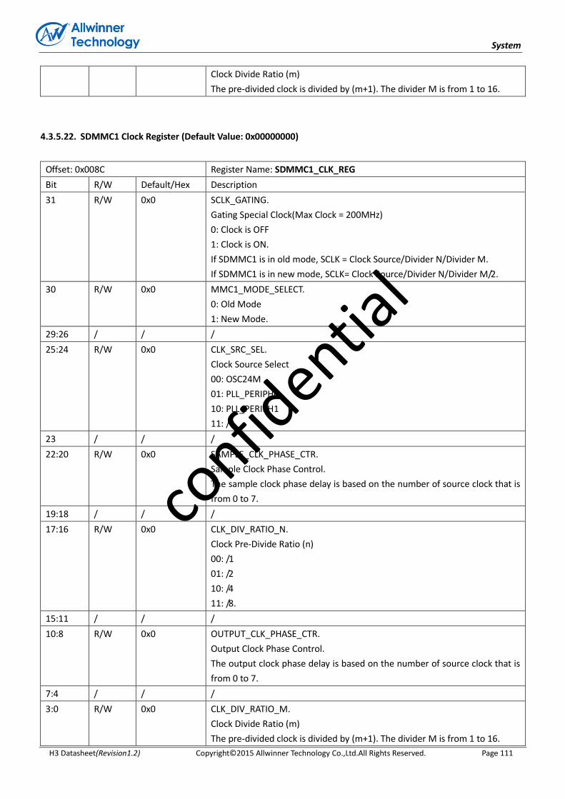
System
H3 Datasheet(Revision1.2) Copyright© 2015 Allwinner Technology Co.,Ltd.All Rights Reserved. Page 111
Clock Divide Ratio (m)
The pre-divided clock is divided by (m+1). The divider M is from 1 to 16.
4.3.5.22. SDMMC1 Clock Register (Default Value: 0x00000000)
Offset: 0x008C Register Name: SDMMC1_CLK_REG
Bit R/W Default/Hex Description
31 R/W 0x0 SCLK_GATING.
Gating Special Clock(Max Clock = 200MHz)
0: Clock is OFF
1: Clock is ON.
If SDMMC1 is in old mode, SCLK = Clock Source/Divider N/Divider M.
If SDMMC1 is in new mode, SCLK= Clock Source/Divider N/Divider M/2.
30 R/W 0x0 MMC1_MODE_SELECT.
0: Old Mode
1: New Mode.
29:26 / / /
25:24 R/W 0x0 CLK_SRC_SEL.
Clock Source Select
00: OSC24M
01: PLL_PERIPH0
10: PLL_PERIPH1
11: /
23 / / /
22:20 R/W 0x0 SAMPLE_CLK_PHASE_CTR.
Sample Clock Phase Control.
The sample clock phase delay is based on the number of source clock that is
from 0 to 7.
19:18 / / /
17:16 R/W 0x0 CLK_DIV_RATIO_N.
Clock Pre-Divide Ratio (n)
00: /1
01: /2
10: /4
11: /8.
15:11 / / /
10:8 R/W 0x0 OUTPUT_CLK_PHASE_CTR.
Output Clock Phase Control.
The output clock phase delay is based on the number of source clock that is
from 0 to 7.
7:4 / / /
3:0 R/W 0x0 CLK_DIV_RATIO_M.
Clock Divide Ratio (m)
The pre-divided clock is divided by (m+1). The divider M is from 1 to 16.
confid
ential

System
H3 Datasheet(Revision1.2) Copyright© 2015 Allwinner Technology Co.,Ltd.All Rights Reserved. Page 112
4.3.5.23. SDMMC2 Clock Register (Default Value: 0x00000000)
Offset: 0x0090 Register Name: SDMMC2_CLK_REG
Bit R/W Default/Hex Description
31 R/W 0x0 SCLK_GATING.
Gating Special Clock(Max Clock = 200MHz)
0: Clock is OFF
1: Clock is ON.
If SDMMC2 is in old mode, SCLK = Clock Source/Divider N/Divider M.
If SDMMC2 is in new mode, SCLK= Clock Source/Divider N/Divider M/2.
30 R/W 0x0 MMC2_MODE_SELECT.
0: Old Mode
1: New Mode.
29:26 / / /
25:24 R/W 0x0 CLK_SRC_SEL.
Clock Source Select
00: OSC24M
01: PLL_PERIPH0
10: PLL_PERIPH1
11: /
23 / / /
22:20 R/W 0x0 CLK_PHASE_CTR.
Sample Clock Phase Control.
The sample clock phase delay is based on the number of source clock that is
from 0 to 7.
19:18 / / /
17:16 R/W 0x0 CLK_DIV_RATIO_N.
Clock Pre Divide Ratio (n)
00: /1
01: /2
10: /4
11: /8.
15:11 / / /
10:8 R/W 0x0 OUTPUT_CLK_PHASE_CTR.
Output Clock Phase Control.
The output clock phase delay is based on the number of source clock that is
from 0 to 7.
7:4 / / /
3:0 R/W 0x0 CLK_DIV_RATIO_M.
Clock Divide Ratio (m)
The pre-divided clock is divided by (m+1). The divider M is from 1 to 16.
confid
ential

System
H3 Datasheet(Revision1.2) Copyright© 2015 Allwinner Technology Co.,Ltd.All Rights Reserved. Page 113
4.3.5.24. TS Clock Register (Default Value: 0x00000000)
Offset: 0x0098 Register Name: TS_CLK_REG
Bit R/W Default/Hex Description
31 R/W 0x0 SCLK_GATING.
Gating Special Clock(Max Clock = 200MHz)
0: Clock is OFF
1: Clock is ON.
SCLK = Clock Source/Divider N/Divider M.
30:28 / / /
27:24 R/W 0x0 CLK_SRC_SEL.
Clock Source Select
0000: OSC24M
0001: PLL_PERIPH0
Others: /
23:18 / / /
17:16 R/W 0x0 CLK_DIV_RATIO_N.
Clock pre-divide ratio (n)
The select clock source is pre-divided by 2^n. The divider is 1/2/4/8.
15:4 / / /
3:0 R/W 0x0 CLK_DIV_RATIO_M.
Clock divide ratio (m)
The pre-divided clock is divided by (m+1). The divider is from 1 to 16.
4.3.5.25. CE Clock Register (Default Value: 0x00000000)
Offset: 0x009C Register Name: CE_CLK_REG
Bit R/W Default/Hex Description
31 R/W 0x0 SCLK_GATING.
Gating Special Clock(Max Clock = 400MHz)
0: Clock is OFF
1: Clock is ON.
SCLK = Clock Source/Divider N/Divider M.
30:26 / / /
25:24 R/W 0x0 CLK_SRC_SEL.
Clock Source Select
00: OSC24M
01: PLL_PERIPH0
10: PLL_PERIPH1
11: /
23:18 / / /
17:16 R/W 0x0 CLK_DIV_RATIO_N.
Clock Pre Divide Ratio (n)
confid
ential
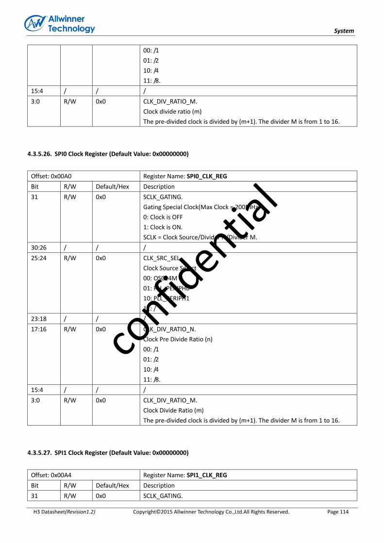
System
H3 Datasheet(Revision1.2) Copyright© 2015 Allwinner Technology Co.,Ltd.All Rights Reserved. Page 114
00: /1
01: /2
10: /4
11: /8.
15:4 / / /
3:0 R/W 0x0 CLK_DIV_RATIO_M.
Clock divide ratio (m)
The pre-divided clock is divided by (m+1). The divider M is from 1 to 16.
4.3.5.26. SPI0 Clock Register (Default Value: 0x00000000)
Offset: 0x00A0 Register Name: SPI0_CLK_REG
Bit R/W Default/Hex Description
31 R/W 0x0 SCLK_GATING.
Gating Special Clock(Max Clock = 200MHz)
0: Clock is OFF
1: Clock is ON.
SCLK = Clock Source/Divider N/Divider M.
30:26 / / /
25:24 R/W 0x0 CLK_SRC_SEL.
Clock Source Select
00: OSC24M
01: PLL_PERIPH0
10: PLL_PERIPH1
11: /
23:18 / / /
17:16 R/W 0x0 CLK_DIV_RATIO_N.
Clock Pre Divide Ratio (n)
00: /1
01: /2
10: /4
11: /8.
15:4 / / /
3:0 R/W 0x0 CLK_DIV_RATIO_M.
Clock Divide Ratio (m)
The pre-divided clock is divided by (m+1). The divider M is from 1 to 16.
4.3.5.27. SPI1 Clock Register (Default Value: 0x00000000)
Offset: 0x00A4 Register Name: SPI1_CLK_REG
Bit R/W Default/Hex Description
31 R/W 0x0 SCLK_GATING.
confid
ential

System
H3 Datasheet(Revision1.2) Copyright© 2015 Allwinner Technology Co.,Ltd.All Rights Reserved. Page 115
Gating Special Clock(Max Clock = 200MHz)
0: Clock is OFF
1: Clock is ON.
SCLK= Clock Source/Divider N/Divider M.
30:26 / / /
25:24 R/W 0x0 CLK_SRC_SEL.
Clock Source Select
00: OSC24M
01: PLL_PERIPH0
10: PLL_PERIPH1
11: /
23:18 / / /
17:16 R/W 0x0 CLK_DIV_RATIO_N.
Clock Pre Divide Ratio (n)
00: /1
01: /2
10: /4
11: /8.
15:4 / / /
3:0 R/W 0x0 CLK_DIV_RATIO_M.
Clock Divide Ratio (m)
The pre-divided clock is divided by (m+1). The divider M is from 1 to 16.
4.3.5.28. I2S/PCM 0 Clock Register (Default Value: 0x00000000)
Offset: 0x00B0 Register Name: I2S/PCM 0_CLK_REG
Bit R/W Default/Hex Description
31 R/W 0x0 SCLK_GATING.
Gating Special Clock(Max Clock = 200MHz)
0: Clock is OFF
1: Clock is ON.
SCLK= Clock Source PLL_AUDIO/Divider M.
30:18 / / /
17:16 R/W 0x0 CLK_SRC_SEL.
00: PLL_AUDIO (8X)
01: PLL_AUDIO(8X)/2
10: PLL_AUDIO(8X)/4
11: PLL_AUDIO
15:0 / / /
confid
ential

System
H3 Datasheet(Revision1.2) Copyright© 2015 Allwinner Technology Co.,Ltd.All Rights Reserved. Page 116
4.3.5.29. I2S/PCM 1 Clock Register (Default Value: 0x00000000)
Offset: 0x00B4 Register Name: I2S/PCM 1_CLK_REG
Bit R/W Default/Hex Description
31 R/W 0x0 SCLK_GATING.
Gating Special Clock(Max Clock = 200MHz)
0: Clock is OFF
1: Clock is ON.
30:18 / / /
17:16 R/W 0x0 CLK_SRC_SEL.
00: PLL_AUDIO (8X)
01: PLL_AUDIO(8X)/2
10: PLL_AUDIO(8X)/4
11: PLL_AUDIO
15:0 / / /
4.3.5.30. I2S/PCM 2 Clock Register (Default Value: 0x00000000)
Offset: 0x00B8 Register Name: I2S/PCM 2_CLK_REG
Bit R/W Default/Hex Description
31 R/W 0x0 SCLK_GATING.
Gating Special Clock(Max Clock = 200MHz)
0: Clock is OFF
1: Clock is ON.
30:18 / / /
17:16 R/W 0x0 CLK_SRC_SEL.
00: PLL_AUDIO (8X)
01: PLL_AUDIO(8X)/2
10: PLL_AUDIO(8X)/4
11: PLL_AUDIO
15:0 / / /
4.3.5.31. OWA Clock Register (Default Value: 0x00000000)
Offset: 0x00C0 Register Name: OWA_CLK_REG
Bit R/W Default/Hex Description
31 R/W 0x0 SCLK_GATING.
Gating Special Clock(Max Clock = 200MHz)
0: Clock is OFF
1: Clock is ON.
SCLK= PLL_AUDIO/Divider M.
30:4 / / /
confid
ential

System
H3 Datasheet(Revision1.2) Copyright© 2015 Allwinner Technology Co.,Ltd.All Rights Reserved. Page 117
3:0 R/W 0x0 CLK_DIV_RATIO_M.
Clock Divide Ratio (m)
The pre-divided clock is divided by (m+1). The divider M is from 1 to 16.
4.3.5.32. USBPHY Configuration Register (Default Value: 0x00000000)
Offset: 0x00CC Register Name: USBPHY_CFG_REG
Bit R/W Default/Hex Description
31:20 / / /
19 R/W 0x0 SCLK_GATING_OHCI3.
Gating Special Clock For OHCI3
0: Clock is OFF
1: Clock is ON
18 R/W 0x0 SCLK_GATING_OHCI2.
Gating Special Clock For OHCI2
0: Clock is OFF
1: Clock is ON
17 R/W 0x0 SCLK_GATING_OHCI1.
Gating Special Clock For OHCI1
0: Clock is OFF
1: Clock is ON
16 R/W 0x0 SCLK_GATING_OTG_OHCI0.
Gating Special Clock For USB OTG_OHCI0
0: Clock is OFF
1: Clock is ON
15:12 / / /
11 R/W 0x0 SCLK_GATING_USBPHY3.
Gating Special Clock For USB PHY3
0: Clock is OFF
1: Clock is ON
10 R/W 0x0 SCLK_GATING_USBPHY2.
Gating Special Clock For USB PHY2
0: Clock is OFF
1: Clock is ON
9 R/W 0x0 SCLK_GATING_USBPHY1.
Gating Special Clock For USB PHY1
0: Clock is OFF
1: Clock is ON
8 R/W 0x0 SCLK_GATING_USBPHY0.
Gating Special Clock For USB PHY0
0: Clock is OFF
1: Clock is ON
7:4 / / /
3 R/W 0x0 USBPHY3_RST.
confid
ential
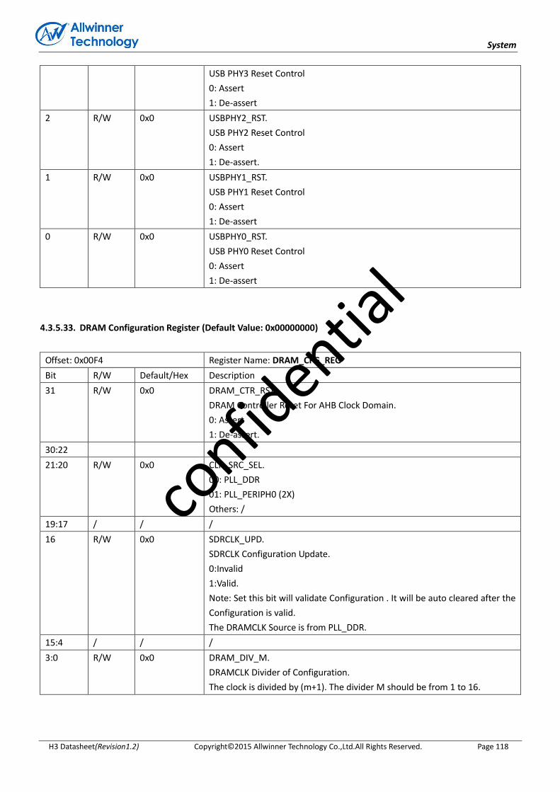
System
H3 Datasheet(Revision1.2) Copyright© 2015 Allwinner Technology Co.,Ltd.All Rights Reserved. Page 118
USB PHY3 Reset Control
0: Assert
1: De-assert
2 R/W 0x0 USBPHY2_RST.
USB PHY2 Reset Control
0: Assert
1: De-assert.
1 R/W 0x0 USBPHY1_RST.
USB PHY1 Reset Control
0: Assert
1: De-assert
0 R/W 0x0 USBPHY0_RST.
USB PHY0 Reset Control
0: Assert
1: De-assert
4.3.5.33. DRAM Configuration Register (Default Value: 0x00000000)
Offset: 0x00F4 Register Name: DRAM_CFG_REG
Bit R/W Default/Hex Description
31 R/W 0x0 DRAM_CTR_RST.
DRAM Controller Reset For AHB Clock Domain.
0: Assert
1: De-assert.
30:22
21:20 R/W 0x0 CLK_SRC_SEL.
00: PLL_DDR
01: PLL_PERIPH0 (2X)
Others: /
19:17 / / /
16 R/W 0x0 SDRCLK_UPD.
SDRCLK Configuration Update.
0:Invalid
1:Valid.
Note: Set this bit will validate Configuration . It will be auto cleared after the
Configuration is valid.
The DRAMCLK Source is from PLL_DDR.
15:4 / / /
3:0 R/W 0x0 DRAM_DIV_M.
DRAMCLK Divider of Configuration.
The clock is divided by (m+1). The divider M should be from 1 to 16.
confid
ential

System
H3 Datasheet(Revision1.2) Copyright© 2015 Allwinner Technology Co.,Ltd.All Rights Reserved. Page 119
4.3.5.34. MBUS Reset Register (Default Value: 0x80000000)
Offset: 0x00FC Register Name: MBUS_RST_REG
Bit R/W Default/Hex Description
31 R/W 0x1 MBUS_RESET.
0: Reset Mbus Domain
1: Assert Mbus Domain.
30:0 / / /
4.3.5.35. DRAM Clock Gating Register (Default Value: 0x00000000)
Offset: 0x0100 Register Name: DRAM_CLK_GATING_REG
Bit R/W Default/Hex Description
31:4 / / /
3 R/W 0x0 TS_DCLK_GATING.
Gating DRAM Clock For TS
0: Mask
1: Pass
2 R/W 0x0 DEINTERLACE_DCLK_GATING.
Gating DRAM SCLK(1X) For DEINTERLACE
0: Mask
1: Pass
1 R/W 0x0 CSI_DCLK_GATING.
Gating DRAM Clock For CSI
0: Mask
1: Pass
0 R/W 0x0 VE_DCLK_GATING.
Gating DRAM Clock For VE
0: Mask
1: Pass
4.3.5.36. DE Clock Gating Register (Default Value: 0x00000000)
Offset: 0x0104 Register Name: DE_CLK_REG
Bit R/W Default/Hex Description
31 R/W 0x0 SCLK_GATING.
Gating Special Clock
0: Clock is OFF
1: Clock is ON
This special clock = Clock Source/Divider M.
30:27 / / /
26:24 R/W 0x0 CLK_SRC_SEL.
confid
ential
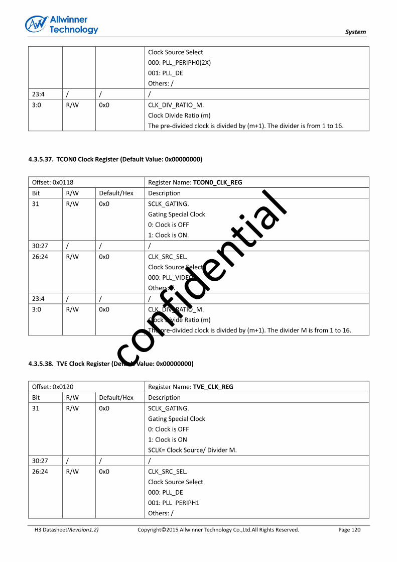
System
H3 Datasheet(Revision1.2) Copyright© 2015 Allwinner Technology Co.,Ltd.All Rights Reserved. Page 120
Clock Source Select
000: PLL_PERIPH0(2X)
001: PLL_DE
Others: /
23:4 / / /
3:0 R/W 0x0 CLK_DIV_RATIO_M.
Clock Divide Ratio (m)
The pre-divided clock is divided by (m+1). The divider is from 1 to 16.
4.3.5.37. TCON0 Clock Register (Default Value: 0x00000000)
Offset: 0x0118 Register Name: TCON0_CLK_REG
Bit R/W Default/Hex Description
31 R/W 0x0 SCLK_GATING.
Gating Special Clock
0: Clock is OFF
1: Clock is ON.
30:27 / / /
26:24 R/W 0x0 CLK_SRC_SEL.
Clock Source Select
000: PLL_VIDEO
Others: /.
23:4 / / /
3:0 R/W 0x0 CLK_DIV_RATIO_M.
Clock Divide Ratio (m)
The pre-divided clock is divided by (m+1). The divider M is from 1 to 16.
4.3.5.38. TVE Clock Register (Default Value: 0x00000000)
Offset: 0x0120 Register Name: TVE_CLK_REG
Bit R/W Default/Hex Description
31 R/W 0x0 SCLK_GATING.
Gating Special Clock
0: Clock is OFF
1: Clock is ON
SCLK= Clock Source/ Divider M.
30:27 / / /
26:24 R/W 0x0 CLK_SRC_SEL.
Clock Source Select
000: PLL_DE
001: PLL_PERIPH1
Others: /
confid
ential
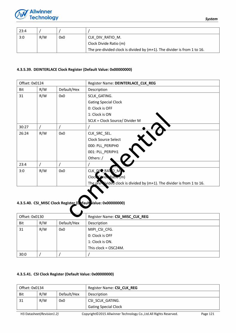
System
H3 Datasheet(Revision1.2) Copyright© 2015 Allwinner Technology Co.,Ltd.All Rights Reserved. Page 121
23:4 / / /
3:0 R/W 0x0 CLK_DIV_RATIO_M.
Clock Divide Ratio (m)
The pre-divided clock is divided by (m+1). The divider is from 1 to 16.
4.3.5.39. DEINTERLACE Clock Register (Default Value: 0x00000000)
Offset: 0x0124 Register Name: DEINTERLACE_CLK_REG
Bit R/W Default/Hex Description
31 R/W 0x0 SCLK_GATING.
Gating Special Clock
0: Clock is OFF
1: Clock is ON
SCLK = Clock Source/ Divider M
30:27 / / /
26:24 R/W 0x0 CLK_SRC_SEL.
Clock Source Select
000: PLL_PERIPH0
001: PLL_PERIPH1
Others: /
23:4 / / /
3:0 R/W 0x0 CLK_DIV_RATIO_M.
Clock Divide Ratio (m)
The pre-divided clock is divided by (m+1). The divider is from 1 to 16.
4.3.5.40. CSI_MISC Clock Register (Default Value: 0x00000000)
Offset: 0x0130 Register Name: CSI_MISC_CLK_REG
Bit R/W Default/Hex Description
31 R/W 0x0 MIPI_CSI_CFG.
0: Clock is OFF
1: Clock is ON.
This clock = OSC24M.
30:0 / / /
4.3.5.41. CSI Clock Register (Default Value: 0x00000000)
Offset: 0x0134 Register Name: CSI_CLK_REG
Bit R/W Default/Hex Description
31 R/W 0x0 CSI_SCLK_GATING.
Gating Special Clock
confid
ential

System
H3 Datasheet(Revision1.2) Copyright© 2015 Allwinner Technology Co.,Ltd.All Rights Reserved. Page 122
0: Clock is OFF
1: Clock is ON.
SCLK= Special Clock Source/CSI_SCLK_DIV_M.
30:27 / / /
26:24 R/W 0x0 SCLK_SRC_SEL.
Special Clock Source Select
000: PLL_PERIPH0
001: PLL_PERIPH1
Others: /
23:20 / / /
19:16 R/W 0x0 CSI_SCLK_DIV_M.
CSI Clock Divide Ratio (m)
The pre-divided clock is divided by (m+1). The divider M is from 1 to 16.
15 R/W 0x0 CSI_MCLK_GATING.
Gating Master Clock
0: Clock is OFF
1: Clock is ON
This clock =Master Clock Source/ CSI_MCLK_DIV_M.
14:11 / / /
10:8 R/W 0x0 MCLK_SRC_SEL.
Master Clock Source Select
000: OSC24M
001: PLL_VIDEO
010: PLL_PERIPH1
Others: /
7:5 / / /
4:0 R/W 0x0 CSI_MCLK_DIV_M.
CSI Master Clock Divide Ratio (m)
The pre-divided clock is divided by (m+1). The divider is from 1 to 32.
4.3.5.42. VE Clock Register (Default Value: 0x00000000)
Offset: 0x013C Register Name: VE_CLK_REG
Bit R/W Default/Hex Description
31 R/W 0x0 VE_SCLK_GATING.
Gating Special Clock
0: Clock is OFF
1: Clock is ON.
SCLK = PLL_VE /Divider N.
30:19 / / /.
18:16 R/W 0x0 CLK_DIV_RATIO_N.
Clock Pre Divide Ratio (N)
The select clock source is pre-divided by n+1. The divider N is from 1 to 8.
15:0 / / /
confid
ential

System
H3 Datasheet(Revision1.2) Copyright© 2015 Allwinner Technology Co.,Ltd.All Rights Reserved. Page 123
4.3.5.43. AC Digital Clock Register (Default Value: 0x00000000)
Offset: 0x0140 Register Name: AC_DIG_CLK_REG
Bit R/W Default/Hex Description
31 R/W 0x0 SCLK_1X_GATING.
Gating Special Clock
0: Clock is OFF
1: Clock is ON
SCLK = PLL_AUDIO Output.
30:0 / / /
4.3.5.44. AVS Clock Register (Default Value: 0x00000000)
Offset: 0x0144 Register Name: AVS_CLK_REG
Bit R/W Default/Hex Description
31 R/W 0x0 SCLK_GATING.
Gating Special Clock
0: Clock is OFF
1: Clock is ON.
SCLK= OSC24M.
30:0 / / /
4.3.5.45. HDMI Clock Register (Default Value: 0x00000000)
Offset: 0x0150 Register Name: HDMI_CLK_REG
Bit R/W Default/Hex Description
31 R/W 0x0 SCLK_GATING.
Gating Special Clock
0: Clock is OFF
1: Clock is ON.
SCLK= Clock Source/ Divider M.
30:26 / / /
25:24 R/W 0x0 SCLK_SEL.
Special Clock Source Select
00: PLL_VIDEO
Others: /
23:4 / / /
3:0 R/W 0x0 CLK_DIV_RATIO_M.
Clock Divide Ratio (m)
The pre-divided clock is divided by (m+1). The divider M is from 1 to 16.
confid
ential

System
H3 Datasheet(Revision1.2) Copyright© 2015 Allwinner Technology Co.,Ltd.All Rights Reserved. Page 124
4.3.5.46. HDMI Slow Clock Register (Default Value: 0x00000000)
Offset: 0x0154 Register Name: HDMI_SLOW_CLK_REG
Bit R/W Default/Hex Description
31 R/W 0x0 HDMI_DDC_CLK_GATING.
0: Clock is OFF
1: Clock is ON.
SCLK = OSC24M.
30:0 / / /
4.3.5.47. MBUS Clock Register (Default Value: 0x00000000)
Offset: 0x015C Register Name: MBUS_CLK_REG
Bit R/W Default/Hex Description
31 R/W 0x0
MBUS_SCLK_GATING.
Gating Clock for MBUS
0: Clock is OFF
1: Clock is ON.
MBUS_CLOCK = Clock Source/Divider M
30:26 / / /
25:24 R/W 0x0
MBUS_SCLK_SRC
Clock Source Select
00: OSC24M
01: PLL_PERIPH0(2X)
10: PLL_DDR
11: /.
23:3 / / /
2:0 R/W 0x0
MBUS_SCLK_RATIO_M
Clock Divide Ratio (m)
The pre-divided clock is divided by (m+1). The divider M is from 1 to 8.
Note: If the clock has been changed ,it must wait for at least 16 cycles.
4.3.5.48. GPU Clock Register (Default Value: 0x00000000)
Offset: 0x01A0 Register Name: GPU_CLK_REG
Bit R/W Default/Hex Description
31 R/W 0x0 SCLK_GATING.
0: Clock is OFF
1: Clock is ON.
SCLK= PLL-GPU/Divider N.
confid
ential

System
H3 Datasheet(Revision1.2) Copyright© 2015 Allwinner Technology Co.,Ltd.All Rights Reserved. Page 125
30:3 / / /.
2:0 R/W 0x0 CLK_DIV_RATIO_N.
Clock Pre Divide Ratio (N)
The select clock source is pre-divided by( n+1). The divider N is from 1 to 8.
4.3.5.49. PLL Stable Time Register0 (Default Value: 0x000000FF)
Offset: 0x0200 Register Name: PLL_STABLE_TIME_REG0
Bit R/W Default/Hex Description
31:16 / / /
15:0 R/W 0x00FF PLL_LOCK_TIME
PLL Lock Time (Unit: us).
Note: When any PLL (except PLL_CPU) is enabled or changed, the
corresponding PLL lock bit will be set after the PLL STABLE Time.
4.3.5.50. PLL Stable Time Register1 (Default Value: 0x000000FF)
Offset: 0x0204 Register Name: PLL_STABLE_TIME_REG1
Bit R/W Default/Hex Description
31:16 / / /
15:0 R/W 0x00FF PLL_CPU_LOCK_TIME
PLL_CPU Lock Time (Unit: us).
Note: When PLL_CPU is enabled or changed, the PLL_CPU lock bit will be set
after the PLL_CPU STABLE Time.
4.3.5.51. PLL_CPUX Bias Register (Default Value: 0x08100200)
Offset: 0x0220 Register Name: PLL_CPUX_BIAS_REG
Bit R/W Default/Hex Description
31 R/W 0x0 VCO_RST.
VCO reset in.
30:29 / / /
28 R/W 0x0 EXG_MODE.
Exchange Mode.
Note: CPU PLL source will select PLL_PERIPH0 instead of PLL_CPU
27:24 R/W 0x8 PLL_VCO_BIAS_CTRL.
PLL VCO Bias Control[3:0].
23:21 / / /
20:16 R/W 0x10 PLL_BIAS_CUR_CTRL.
PLL Bias Current Control[4:0].
15:11 / / /
confid
ential
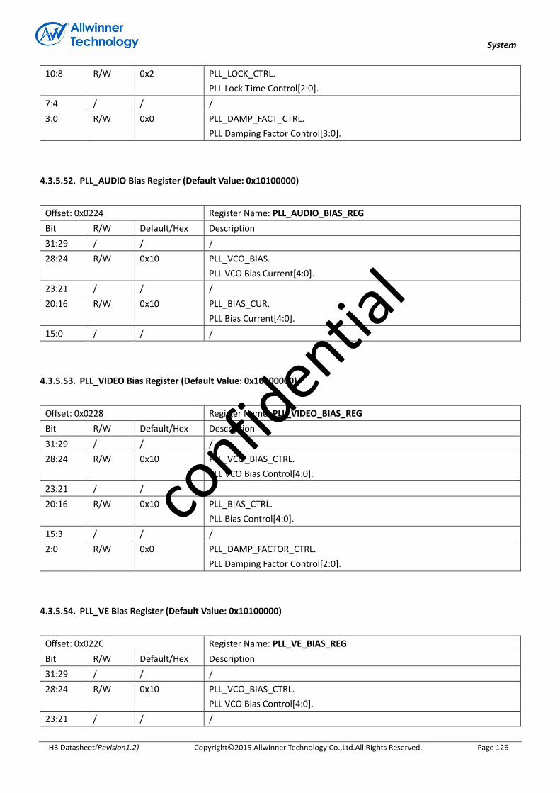
System
H3 Datasheet(Revision1.2) Copyright© 2015 Allwinner Technology Co.,Ltd.All Rights Reserved. Page 126
10:8 R/W 0x2 PLL_LOCK_CTRL.
PLL Lock Time Control[2:0].
7:4 / / /
3:0 R/W 0x0 PLL_DAMP_FACT_CTRL.
PLL Damping Factor Control[3:0].
4.3.5.52. PLL_AUDIO Bias Register (Default Value: 0x10100000)
Offset: 0x0224 Register Name: PLL_AUDIO_BIAS_REG
Bit R/W Default/Hex Description
31:29 / / /
28:24 R/W 0x10 PLL_VCO_BIAS.
PLL VCO Bias Current[4:0].
23:21 / / /
20:16 R/W 0x10 PLL_BIAS_CUR.
PLL Bias Current[4:0].
15:0 / / /
4.3.5.53. PLL_VIDEO Bias Register (Default Value: 0x10100000)
Offset: 0x0228 Register Name: PLL_VIDEO_BIAS_REG
Bit R/W Default/Hex Description
31:29 / / /
28:24 R/W 0x10 PLL_VCO_BIAS_CTRL.
PLL VCO Bias Control[4:0].
23:21 / / /
20:16 R/W 0x10 PLL_BIAS_CTRL.
PLL Bias Control[4:0].
15:3 / / /
2:0 R/W 0x0 PLL_DAMP_FACTOR_CTRL.
PLL Damping Factor Control[2:0].
4.3.5.54. PLL_VE Bias Register (Default Value: 0x10100000)
Offset: 0x022C Register Name: PLL_VE_BIAS_REG
Bit R/W Default/Hex Description
31:29 / / /
28:24 R/W 0x10 PLL_VCO_BIAS_CTRL.
PLL VCO Bias Control[4:0].
23:21 / / /
confid
ential
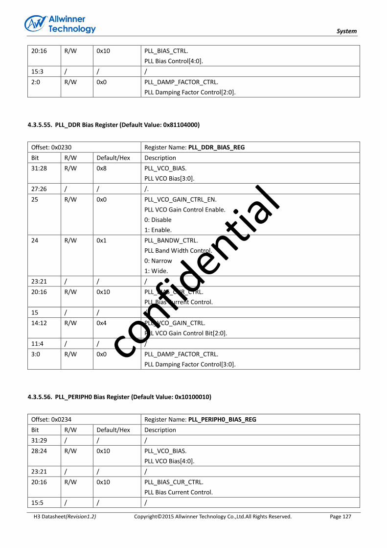
System
H3 Datasheet(Revision1.2) Copyright© 2015 Allwinner Technology Co.,Ltd.All Rights Reserved. Page 127
20:16 R/W 0x10 PLL_BIAS_CTRL.
PLL Bias Control[4:0].
15:3 / / /
2:0 R/W 0x0 PLL_DAMP_FACTOR_CTRL.
PLL Damping Factor Control[2:0].
4.3.5.55. PLL_DDR Bias Register (Default Value: 0x81104000)
Offset: 0x0230 Register Name: PLL_DDR_BIAS_REG
Bit R/W Default/Hex Description
31:28 R/W 0x8 PLL_VCO_BIAS.
PLL VCO Bias[3:0].
27:26 / / /.
25 R/W 0x0 PLL_VCO_GAIN_CTRL_EN.
PLL VCO Gain Control Enable.
0: Disable
1: Enable.
24 R/W 0x1 PLL_BANDW_CTRL.
PLL Band Width Control.
0: Narrow
1: Wide.
23:21 / / /
20:16 R/W 0x10 PLL_BIAS_CUR_CTRL.
PLL Bias Current Control.
15 / / /
14:12 R/W 0x4 PLL_VCO_GAIN_CTRL.
PLL VCO Gain Control Bit[2:0].
11:4 / / /
3:0 R/W 0x0 PLL_DAMP_FACTOR_CTRL.
PLL Damping Factor Control[3:0].
4.3.5.56. PLL_PERIPH0 Bias Register (Default Value: 0x10100010)
Offset: 0x0234 Register Name: PLL_PERIPH0_BIAS_REG
Bit R/W Default/Hex Description
31:29 / / /
28:24 R/W 0x10 PLL_VCO_BIAS.
PLL VCO Bias[4:0].
23:21 / / /
20:16 R/W 0x10 PLL_BIAS_CUR_CTRL.
PLL Bias Current Control.
15:5 / / /
confid
ential
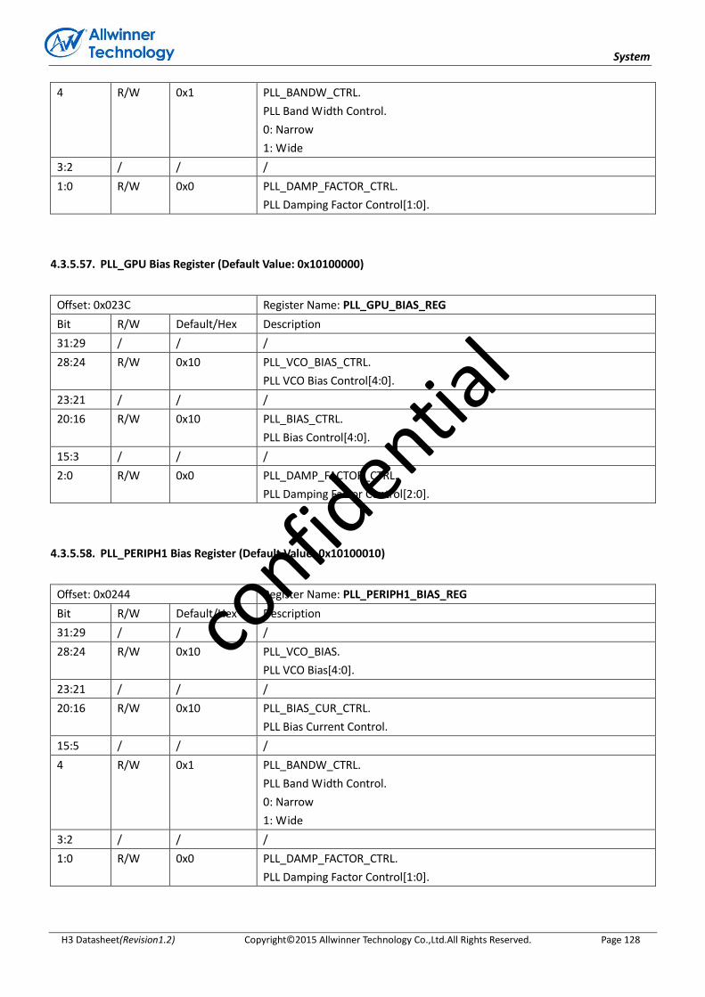
System
H3 Datasheet(Revision1.2) Copyright© 2015 Allwinner Technology Co.,Ltd.All Rights Reserved. Page 128
4 R/W 0x1 PLL_BANDW_CTRL.
PLL Band Width Control.
0: Narrow
1: Wide
3:2 / / /
1:0 R/W 0x0 PLL_DAMP_FACTOR_CTRL.
PLL Damping Factor Control[1:0].
4.3.5.57. PLL_GPU Bias Register (Default Value: 0x10100000)
Offset: 0x023C Register Name: PLL_GPU_BIAS_REG
Bit R/W Default/Hex Description
31:29 / / /
28:24 R/W 0x10 PLL_VCO_BIAS_CTRL.
PLL VCO Bias Control[4:0].
23:21 / / /
20:16 R/W 0x10 PLL_BIAS_CTRL.
PLL Bias Control[4:0].
15:3 / / /
2:0 R/W 0x0 PLL_DAMP_FACTOR_CTRL.
PLL Damping Factor Control[2:0].
4.3.5.58. PLL_PERIPH1 Bias Register (Default Value: 0x10100010)
Offset: 0x0244 Register Name: PLL_PERIPH1_BIAS_REG
Bit R/W Default/Hex Description
31:29 / / /
28:24 R/W 0x10 PLL_VCO_BIAS.
PLL VCO Bias[4:0].
23:21 / / /
20:16 R/W 0x10 PLL_BIAS_CUR_CTRL.
PLL Bias Current Control.
15:5 / / /
4 R/W 0x1 PLL_BANDW_CTRL.
PLL Band Width Control.
0: Narrow
1: Wide
3:2 / / /
1:0 R/W 0x0 PLL_DAMP_FACTOR_CTRL.
PLL Damping Factor Control[1:0].
confid
ential
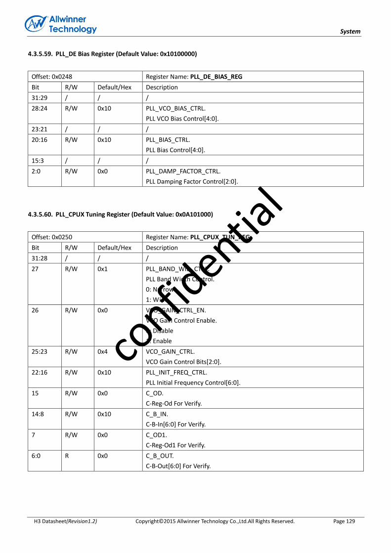
System
H3 Datasheet(Revision1.2) Copyright© 2015 Allwinner Technology Co.,Ltd.All Rights Reserved. Page 129
4.3.5.59. PLL_DE Bias Register (Default Value: 0x10100000)
Offset: 0x0248 Register Name: PLL_DE_BIAS_REG
Bit R/W Default/Hex Description
31:29 / / /
28:24 R/W 0x10 PLL_VCO_BIAS_CTRL.
PLL VCO Bias Control[4:0].
23:21 / / /
20:16 R/W 0x10 PLL_BIAS_CTRL.
PLL Bias Control[4:0].
15:3 / / /
2:0 R/W 0x0 PLL_DAMP_FACTOR_CTRL.
PLL Damping Factor Control[2:0].
4.3.5.60. PLL_CPUX Tuning Register (Default Value: 0x0A101000)
Offset: 0x0250 Register Name: PLL_CPUX_TUN_REG
Bit R/W Default/Hex Description
31:28 / / /
27 R/W 0x1 PLL_BAND_WID_CTRL.
PLL Band Width Control.
0: Narrow
1: Wide
26 R/W 0x0 VCO_GAIN_CTRL_EN.
VCO Gain Control Enable.
0: Disable
1: Enable
25:23 R/W 0x4 VCO_GAIN_CTRL.
VCO Gain Control Bits[2:0].
22:16 R/W 0x10 PLL_INIT_FREQ_CTRL.
PLL Initial Frequency Control[6:0].
15 R/W 0x0 C_OD.
C-Reg-Od For Verify.
14:8 R/W 0x10 C_B_IN.
C-B-In[6:0] For Verify.
7 R/W 0x0 C_OD1.
C-Reg-Od1 For Verify.
6:0 R 0x0 C_B_OUT.
C-B-Out[6:0] For Verify.
confid
ential
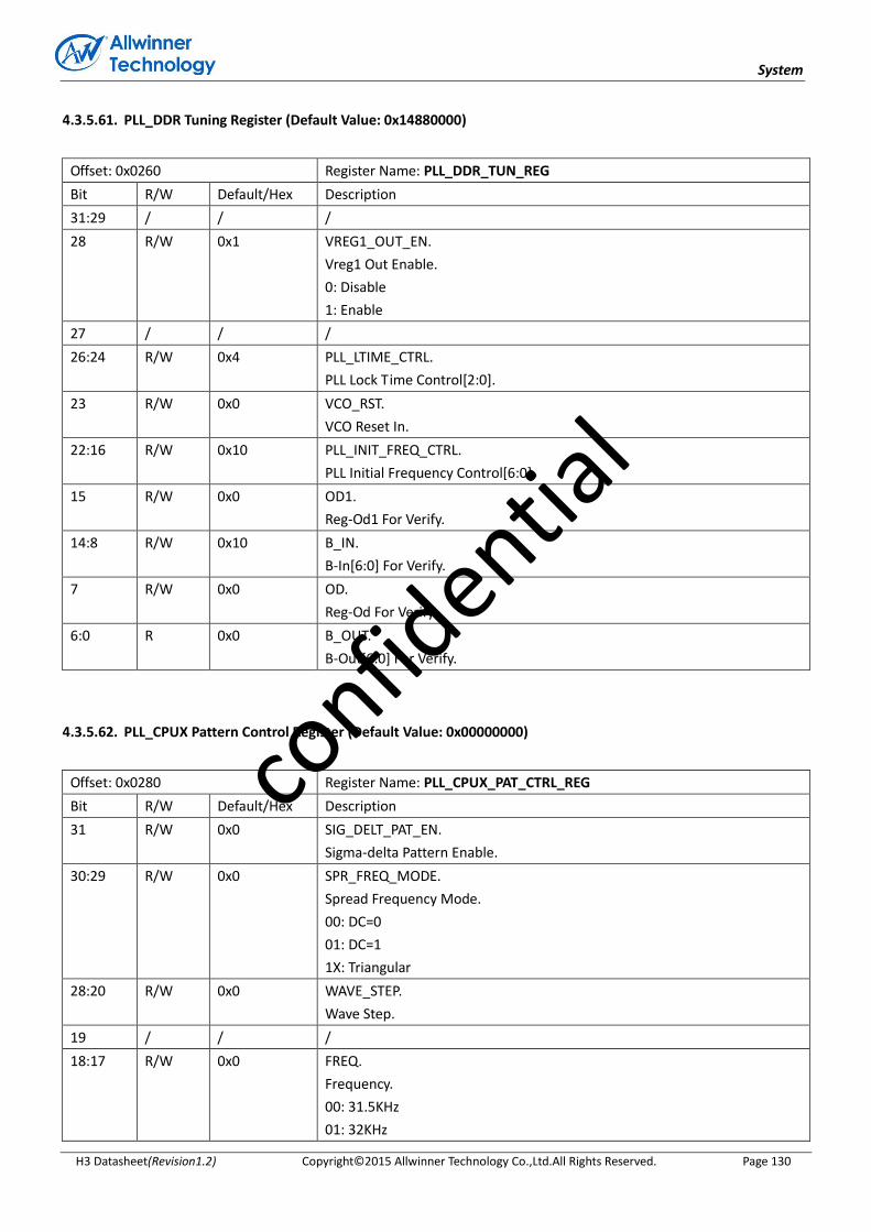
System
H3 Datasheet(Revision1.2) Copyright© 2015 Allwinner Technology Co.,Ltd.All Rights Reserved. Page 130
4.3.5.61. PLL_DDR Tuning Register (Default Value: 0x14880000)
Offset: 0x0260 Register Name: PLL_DDR_TUN_REG
Bit R/W Default/Hex Description
31:29 / / /
28 R/W 0x1 VREG1_OUT_EN.
Vreg1 Out Enable.
0: Disable
1: Enable
27 / / /
26:24 R/W 0x4 PLL_LTIME_CTRL.
PLL Lock Time Control[2:0].
23 R/W 0x0 VCO_RST.
VCO Reset In.
22:16 R/W 0x10 PLL_INIT_FREQ_CTRL.
PLL Initial Frequency Control[6:0].
15 R/W 0x0 OD1.
Reg-Od1 For Verify.
14:8 R/W 0x10 B_IN.
B-In[6:0] For Verify.
7 R/W 0x0 OD.
Reg-Od For Verify.
6:0 R 0x0 B_OUT.
B-Out[6:0] For Verify.
4.3.5.62. PLL_CPUX Pattern Control Register (Default Value: 0x00000000)
Offset: 0x0280 Register Name: PLL_CPUX_PAT_CTRL_REG
Bit R/W Default/Hex Description
31 R/W 0x0 SIG_DELT_PAT_EN.
Sigma-delta Pattern Enable.
30:29 R/W 0x0 SPR_FREQ_MODE.
Spread Frequency Mode.
00: DC=0
01: DC=1
1X: Triangular
28:20 R/W 0x0 WAVE_STEP.
Wave Step.
19 / / /
18:17 R/W 0x0 FREQ.
Frequency.
00: 31.5KHz
01: 32KHz
confid
ential

System
H3 Datasheet(Revision1.2) Copyright© 2015 Allwinner Technology Co.,Ltd.All Rights Reserved. Page 131
10: 32.5KHz
11: 33KHz
16:0 R/W 0x0 WAVE_BOT.
Wave Bottom.
4.3.5.63. PLL_AUDIO Pattern Control Register(Default Value: 0x00000000)
Offset: 0x0284 Register Name: PLL_AUDIO_PAT_CTRL_REG
Bit R/W Default/Hex Description
31 R/W 0x0 SIG_DELT_PAT_EN.
Sigma-delta Pattern Enable.
30:29 R/W 0x0 SPR_FREQ_MODE.
Spread Frequency Mode.
00: DC=0
01: DC=1
1X: Triangular
28:20 R/W 0x0 WAVE_STEP.
Wave Step.
19 / / /
18:17 R/W 0x0 FREQ.
Frequency.
00: 31.5KHz
01: 32KHz
10: 32.5KHz
11: 33KHz
16:0 R/W 0x0 WAVE_BOT.
Wave Bottom.
4.3.5.64. PLL_VIDEO Pattern Control Register (Default Value: 0x00000000)
Offset: 0x0288 Register Name: PLL_VIDEO_PAT_CTRL_REG
Bit R/W Default/Hex Description
31 R/W 0x0 SIG_DELT_PAT_EN.
Sigma-delta Pattern Enable.
30:29 R/W 0x0 SPR_FREQ_MODE.
Spread Frequency Mode.
00: DC=0
01: DC=1
1X: Triangular
28:20 R/W 0x0 WAVE_STEP.
Wave Step.
19 / / /
confid
ential

System
H3 Datasheet(Revision1.2) Copyright© 2015 Allwinner Technology Co.,Ltd.All Rights Reserved. Page 132
18:17 R/W 0x0 FREQ.
Frequency.
00: 31.5KHz
01: 32KHz
10: 32.5KHz
11: 33KHz
16:0 R/W 0x0 WAVE_BOT.
Wave Bottom.
4.3.5.65. PLL_VE Pattern Control Register (Default Value: 0x00000000)
Offset: 0x028C Register Name: PLL_VE_PAT_CTRL_REG
Bit R/W Default/Hex Description
31 R/W 0x0 SIG_DELT_PAT_EN.
Sigma-delta Pattern Enable.
30:29 R/W 0x0 SPR_FREQ_MODE.
Spread Frequency Mode.
00: DC=0
01: DC=1
1X: Triangular
28:20 R/W 0x0 WAVE_STEP.
Wave Step.
19 / / /
18:17 R/W 0x0 FREQ.
Frequency.
00: 31.5KHz
01: 32KHz
10: 32.5KHz
11: 33KHz
16:0 R/W 0x0 WAVE_BOT.
Wave Bottom.
4.3.5.66. PLL_DDR Pattern Control Register (Default Value: 0x00000000)
Offset: 0x0290 Register Name: PLL_DDR_PAT_CTRL_REG
Bit R/W Default/Hex Description
31 R/W 0x0 SIG_DELT_PAT_EN.
Sigma-delta Pattern Enable.
30:29 R/W 0x0 SPR_FREQ_MODE.
Spread Frequency Mode.
00: DC=0
01: DC=1
1X: Triangular
confid
ential
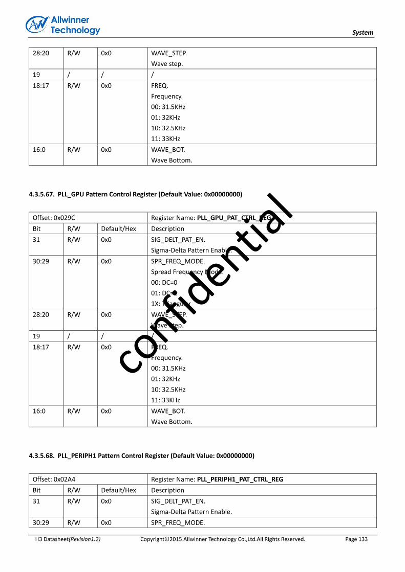
System
H3 Datasheet(Revision1.2) Copyright© 2015 Allwinner Technology Co.,Ltd.All Rights Reserved. Page 133
28:20 R/W 0x0 WAVE_STEP.
Wave step.
19 / / /
18:17 R/W 0x0 FREQ.
Frequency.
00: 31.5KHz
01: 32KHz
10: 32.5KHz
11: 33KHz
16:0 R/W 0x0 WAVE_BOT.
Wave Bottom.
4.3.5.67. PLL_GPU Pattern Control Register (Default Value: 0x00000000)
Offset: 0x029C Register Name: PLL_GPU_PAT_CTRL_REG
Bit R/W Default/Hex Description
31 R/W 0x0 SIG_DELT_PAT_EN.
Sigma-Delta Pattern Enable.
30:29 R/W 0x0 SPR_FREQ_MODE.
Spread Frequency Mode.
00: DC=0
01: DC=1
1X: Triangular
28:20 R/W 0x0 WAVE_STEP.
Wave Step.
19 / / /
18:17 R/W 0x0 FREQ.
Frequency.
00: 31.5KHz
01: 32KHz
10: 32.5KHz
11: 33KHz
16:0 R/W 0x0 WAVE_BOT.
Wave Bottom.
4.3.5.68. PLL_PERIPH1 Pattern Control Register (Default Value: 0x00000000)
Offset: 0x02A4 Register Name: PLL_PERIPH1_PAT_CTRL_REG
Bit R/W Default/Hex Description
31 R/W 0x0 SIG_DELT_PAT_EN.
Sigma-Delta Pattern Enable.
30:29 R/W 0x0 SPR_FREQ_MODE.
confid
ential
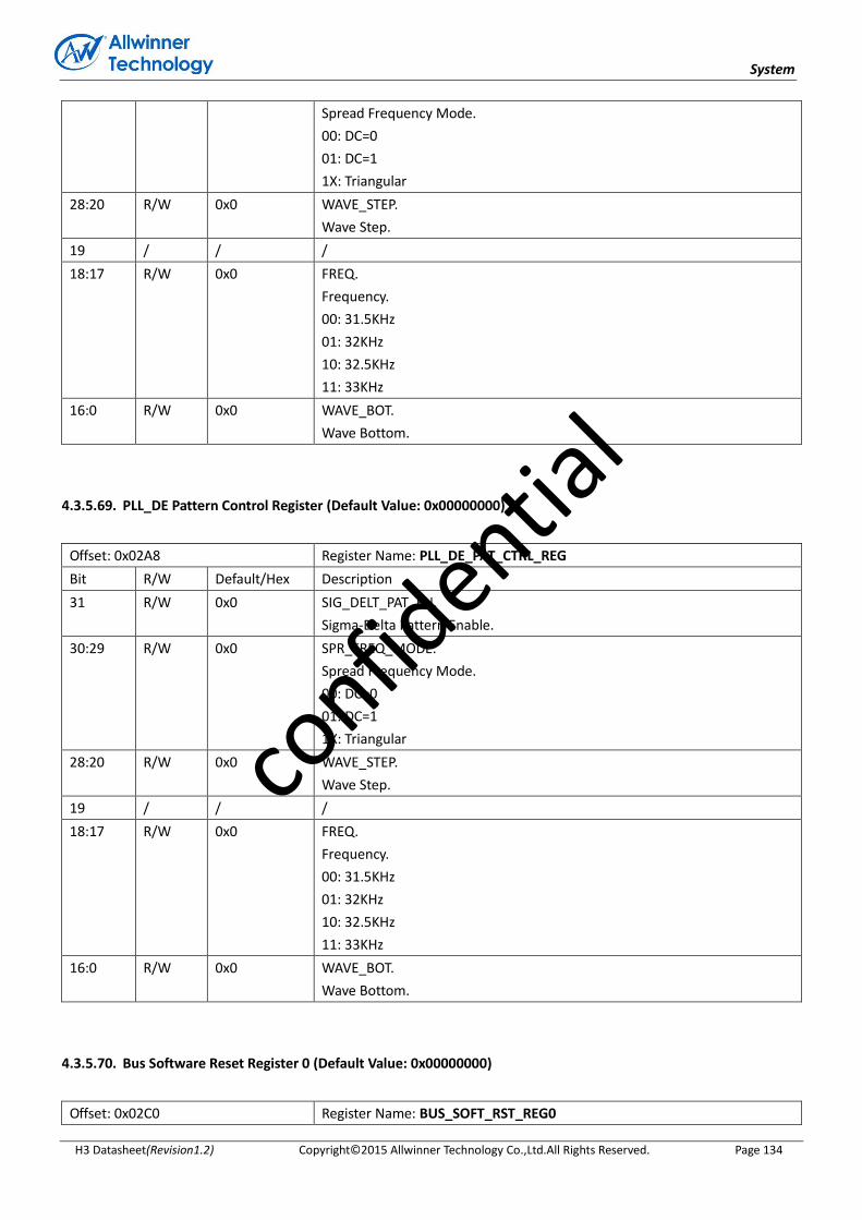
System
H3 Datasheet(Revision1.2) Copyright© 2015 Allwinner Technology Co.,Ltd.All Rights Reserved. Page 134
Spread Frequency Mode.
00: DC=0
01: DC=1
1X: Triangular
28:20 R/W 0x0 WAVE_STEP.
Wave Step.
19 / / /
18:17 R/W 0x0 FREQ.
Frequency.
00: 31.5KHz
01: 32KHz
10: 32.5KHz
11: 33KHz
16:0 R/W 0x0 WAVE_BOT.
Wave Bottom.
4.3.5.69. PLL_DE Pattern Control Register (Default Value: 0x00000000)
Offset: 0x02A8 Register Name: PLL_DE_PAT_CTRL_REG
Bit R/W Default/Hex Description
31 R/W 0x0 SIG_DELT_PAT_EN.
Sigma-Delta Pattern Enable.
30:29 R/W 0x0 SPR_FREQ_MODE.
Spread Frequency Mode.
00: DC=0
01: DC=1
1X: Triangular
28:20 R/W 0x0 WAVE_STEP.
Wave Step.
19 / / /
18:17 R/W 0x0 FREQ.
Frequency.
00: 31.5KHz
01: 32KHz
10: 32.5KHz
11: 33KHz
16:0 R/W 0x0 WAVE_BOT.
Wave Bottom.
4.3.5.70. Bus Software Reset Register 0 (Default Value: 0x00000000)
Offset: 0x02C0 Register Name: BUS_SOFT_RST_REG0
confid
ential
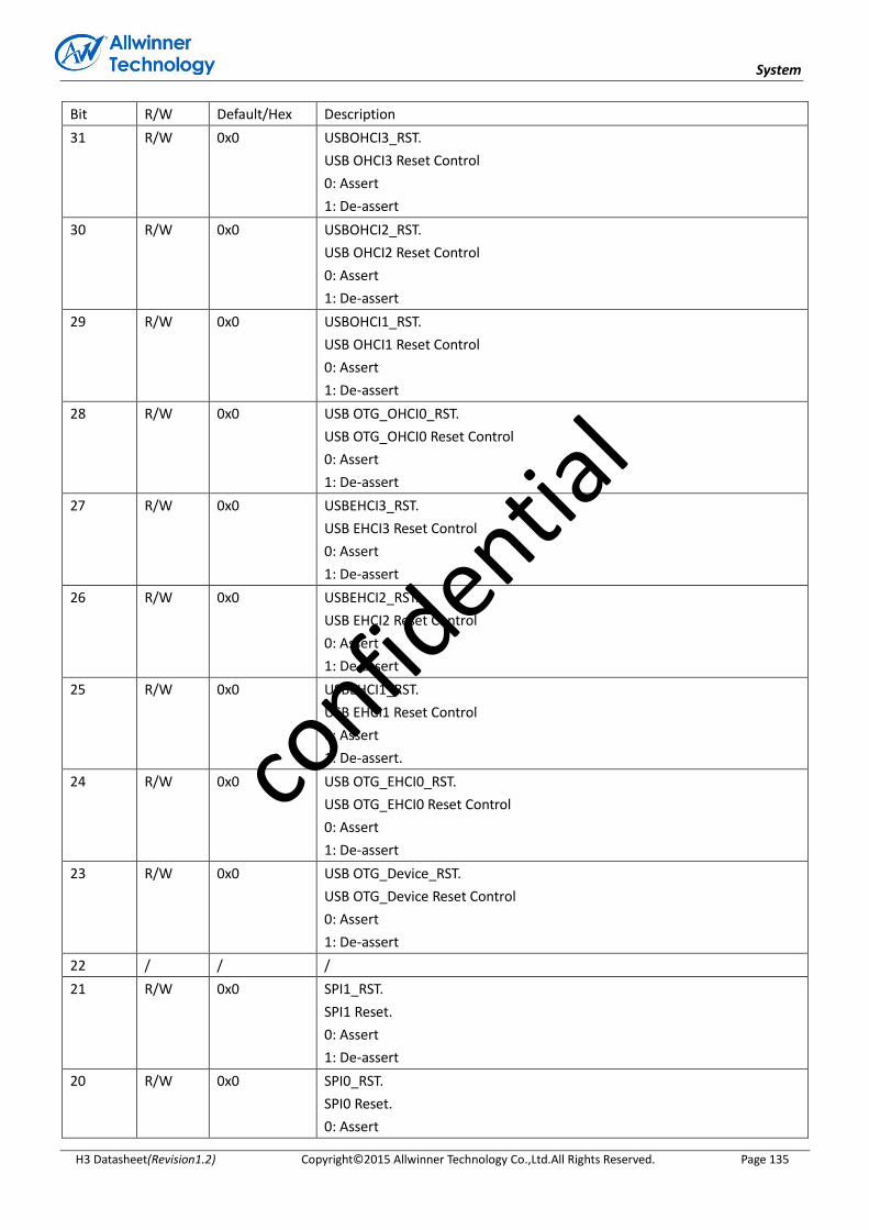
System
H3 Datasheet(Revision1.2) Copyright© 2015 Allwinner Technology Co.,Ltd.All Rights Reserved. Page 135
Bit R/W Default/Hex Description
31 R/W 0x0 USBOHCI3_RST.
USB OHCI3 Reset Control
0: Assert
1: De-assert
30 R/W 0x0 USBOHCI2_RST.
USB OHCI2 Reset Control
0: Assert
1: De-assert
29 R/W 0x0 USBOHCI1_RST.
USB OHCI1 Reset Control
0: Assert
1: De-assert
28 R/W 0x0 USB OTG_OHCI0_RST.
USB OTG_OHCI0 Reset Control
0: Assert
1: De-assert
27 R/W 0x0 USBEHCI3_RST.
USB EHCI3 Reset Control
0: Assert
1: De-assert
26 R/W 0x0 USBEHCI2_RST.
USB EHCI2 Reset Control
0: Assert
1: De-assert
25 R/W 0x0 USBEHCI1_RST.
USB EHCI1 Reset Control
0: Assert
1: De-assert.
24 R/W 0x0 USB OTG_EHCI0_RST.
USB OTG_EHCI0 Reset Control
0: Assert
1: De-assert
23 R/W 0x0 USB OTG_Device_RST.
USB OTG_Device Reset Control
0: Assert
1: De-assert
22 / / /
21 R/W 0x0 SPI1_RST.
SPI1 Reset.
0: Assert
1: De-assert
20 R/W 0x0 SPI0_RST.
SPI0 Reset.
0: Assert
confid
ential

System
H3 Datasheet(Revision1.2) Copyright© 2015 Allwinner Technology Co.,Ltd.All Rights Reserved. Page 136
1: De-assert
19 R/W 0x0 HSTMR_RST.
HSTMR Reset.
0: Assert
1: De-assert
18 R/W 0x0 TS_RST.
TS Reset.
0: Assert
1: De-assert
17 R/W 0x0 EMAC_RST.
EMAC Reset.
0: Assert
1: De-assert
16:15 / / /
14 R/W 0x0 SDRAM_RST.
SDRAM AHB Reset.
0: Assert
1: De-assert
13 R/W 0x0 NAND_RST.
NAND Reset.
0: Assert
1: De-assert
12:11 / / /
10 R/W 0x0 SD2_RST.
SD/MMC2 Reset.
0: Assert
1: De-assert
9 R/W 0x0 SD1_RST.
SD/MMC1 Reset.
0: Assert
1: De-assert
8 R/W 0x0 SD0_RST.
SD/MMC0 Reset.
0: Assert
1: De-assert
7 / / /
6 R/W 0x0 DMA_RST.
DMA Reset.
0: Assert
1: De-assert
5 R/W 0x0 CE_RST.
CE Reset.
0: Assert
1: De-assert
4:0 / / /
confid
ential
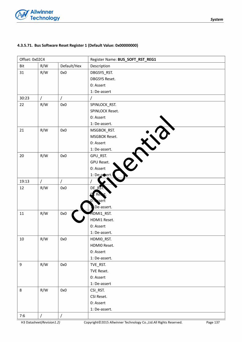
System
H3 Datasheet(Revision1.2) Copyright© 2015 Allwinner Technology Co.,Ltd.All Rights Reserved. Page 137
4.3.5.71. Bus Software Reset Register 1 (Default Value: 0x00000000)
Offset: 0x02C4 Register Name: BUS_SOFT_RST_REG1
Bit R/W Default/Hex Description
31 R/W 0x0 DBGSYS_RST.
DBGSYS Reset.
0: Assert
1: De-assert
30:23 / / /
22 R/W 0x0 SPINLOCK_RST.
SPINLOCK Reset.
0: Assert
1: De-assert.
21 R/W 0x0 MSGBOX_RST.
MSGBOX Reset.
0: Assert
1: De-assert.
20 R/W 0x0 GPU_RST.
GPU Reset.
0: Assert
1: De-assert.
19:13 / / /
12 R/W 0x0 DE_RST.
DE Reset.
0: Assert
1: De-assert.
11 R/W 0x0 HDMI1_RST.
HDMI1 Reset.
0: Assert
1: De-assert.
10 R/W 0x0 HDMI0_RST.
HDMI0 Reset.
0: Assert
1: De-assert.
9 R/W 0x0 TVE_RST.
TVE Reset.
0: Assert
1: De-assert
8 R/W 0x0 CSI_RST.
CSI Reset.
0: Assert
1: De-assert.
7:6 / /
confid
ential
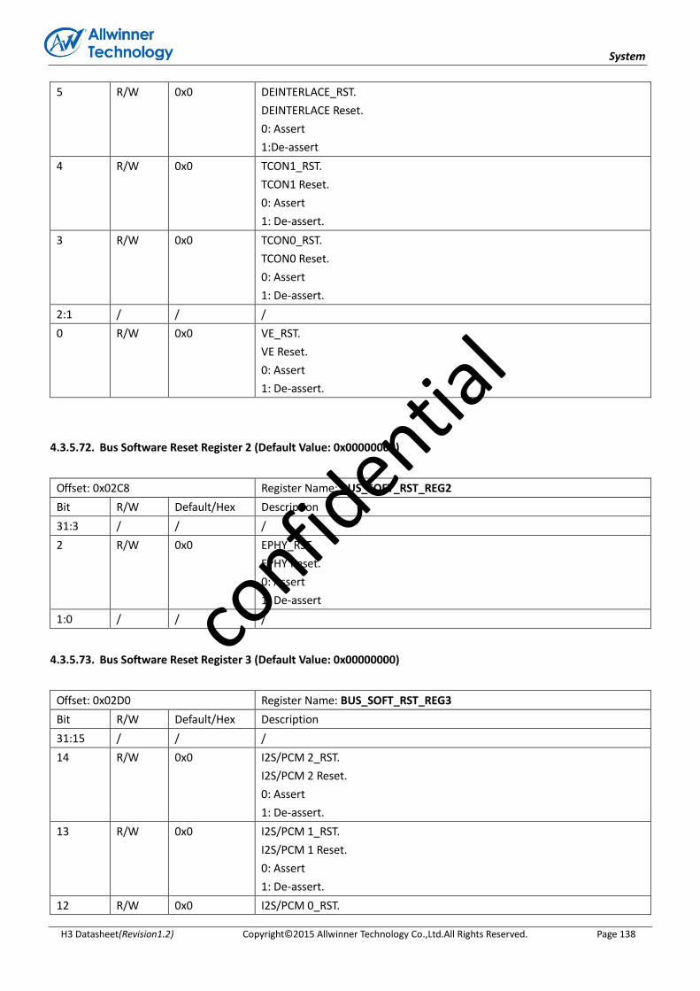
System
H3 Datasheet(Revision1.2) Copyright© 2015 Allwinner Technology Co.,Ltd.All Rights Reserved. Page 138
5 R/W 0x0 DEINTERLACE_RST.
DEINTERLACE Reset.
0: Assert
1:De-assert
4 R/W 0x0 TCON1_RST.
TCON1 Reset.
0: Assert
1: De-assert.
3 R/W 0x0 TCON0_RST.
TCON0 Reset.
0: Assert
1: De-assert.
2:1 / / /
0 R/W 0x0 VE_RST.
VE Reset.
0: Assert
1: De-assert.
4.3.5.72. Bus Software Reset Register 2 (Default Value: 0x00000000)
Offset: 0x02C8 Register Name: BUS_SOFT_RST_REG2
Bit R/W Default/Hex Description
31:3 / / /
2 R/W 0x0 EPHY_RST.
EPHY Reset.
0: Assert
1: De-assert
1:0 / / /
4.3.5.73. Bus Software Reset Register 3 (Default Value: 0x00000000)
Offset: 0x02D0 Register Name: BUS_SOFT_RST_REG3
Bit R/W Default/Hex Description
31:15 / / /
14 R/W 0x0 I2S/PCM 2_RST.
I2S/PCM 2 Reset.
0: Assert
1: De-assert.
13 R/W 0x0 I2S/PCM 1_RST.
I2S/PCM 1 Reset.
0: Assert
1: De-assert.
12 R/W 0x0 I2S/PCM 0_RST.
confid
ential
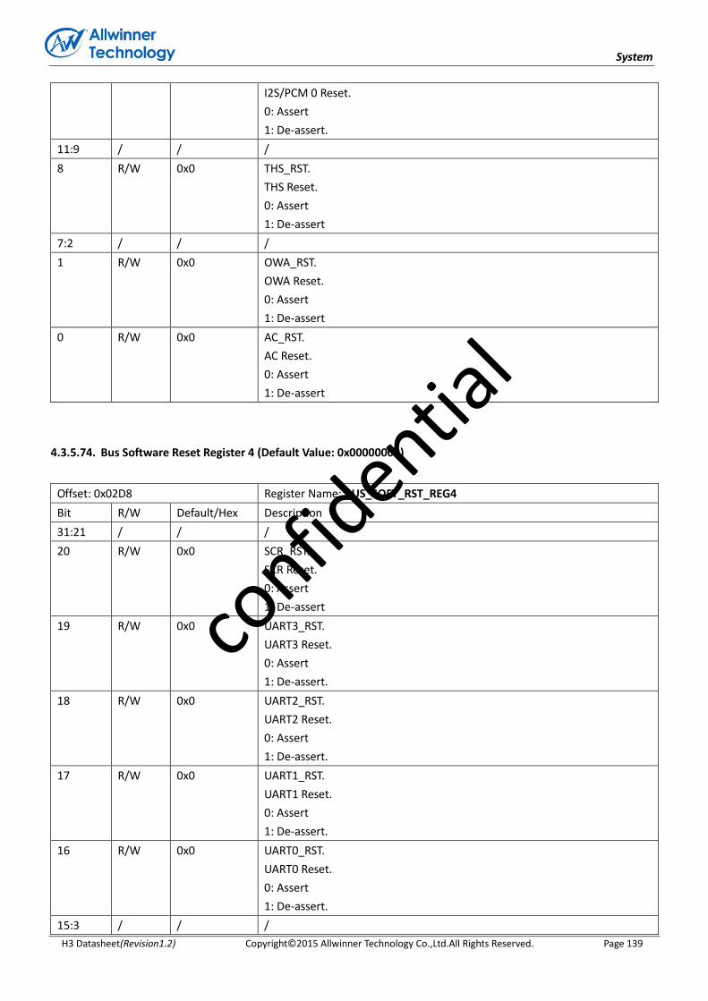
System
H3 Datasheet(Revision1.2) Copyright© 2015 Allwinner Technology Co.,Ltd.All Rights Reserved. Page 139
I2S/PCM 0 Reset.
0: Assert
1: De-assert.
11:9 / / /
8 R/W 0x0 THS_RST.
THS Reset.
0: Assert
1: De-assert
7:2 / / /
1 R/W 0x0 OWA_RST.
OWA Reset.
0: Assert
1: De-assert
0 R/W 0x0 AC_RST.
AC Reset.
0: Assert
1: De-assert
4.3.5.74. Bus Software Reset Register 4 (Default Value: 0x00000000)
Offset: 0x02D8 Register Name: BUS_SOFT_RST_REG4
Bit R/W Default/Hex Description
31:21 / / /
20 R/W 0x0 SCR_RST.
SCR Reset.
0: Assert
1: De-assert
19 R/W 0x0 UART3_RST.
UART3 Reset.
0: Assert
1: De-assert.
18 R/W 0x0 UART2_RST.
UART2 Reset.
0: Assert
1: De-assert.
17 R/W 0x0 UART1_RST.
UART1 Reset.
0: Assert
1: De-assert.
16 R/W 0x0 UART0_RST.
UART0 Reset.
0: Assert
1: De-assert.
15:3 / / /
confid
ential

System
H3 Datasheet(Revision1.2) Copyright© 2015 Allwinner Technology Co.,Ltd.All Rights Reserved. Page 140
2 R/W 0x0 TWI2_RST.
TWI2 Reset.
0: Assert
1: De-assert.
1 R/W 0x0 TWI1_RST.
TWI1 Reset.
0: Assert
1: De-assert.
0 R/W 0x0 TWI0_RST.
TWI0 Reset.
0: Assert
1: De-assert.
4.3.5.75. CCU Security Switch Register (Default Value: 0x00000000)
Offset: 0x02F0 Register Name: CCU_SEC_SWITCH_REG
Bit R/W Default/Hex Description
31:3 / / /
2 R/W 0x0 MBUS_SEC
MBUS clock register security
0:Secure
1:Non-secure
Including MBUS Reset Register and MBUS Clock Register
1 R/W 0x0 BUS_SEC
Bus relevant registers’ security
0:Secure
1:Non-secure
Including AXI/AHB/APB relevant registers,such as CPUX/AXI Configuration
Register,AHB1/APB1 Configuration Register,APB2 Configuration Register,
AHB2 Configuration Register.
0 R/W 0x0 PLL_SEC
PLL relevant registers’ security.
0:Secure
1:Non-secure
Including PLL_CPUX Control Register,PLL_AUDIO Control Register,PLL_VIDEO
Control Register,PLL_VE Control Register,PLL_DDR Control Register,PLL_
PEPIPH0 Control Register,PLL_GPU Control Register,PLL_PERIPH1 Control
Register,PLL_DE Control Register and offset from 0x200 to 0x2A8 relevant
registers.
4.3.5.76. PS Control Register (Default Value: 0x00000000)
Offset: 0x0300 Register Name: PS_CTRL_REG
confid
ential
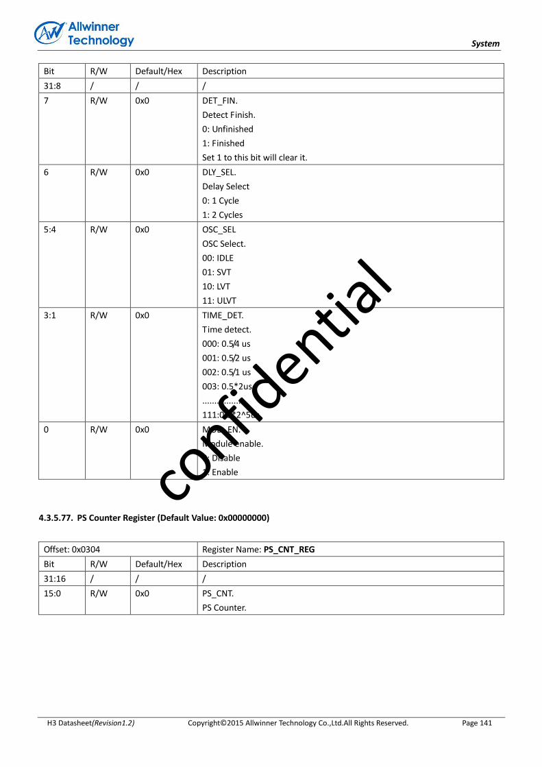
System
H3 Datasheet(Revision1.2) Copyright© 2015 Allwinner Technology Co.,Ltd.All Rights Reserved. Page 141
Bit R/W Default/Hex Description
31:8 / / /
7 R/W 0x0 DET_FIN.
Detect Finish.
0: Unfinished
1: Finished
Set 1 to this bit will clear it.
6 R/W 0x0 DLY_SEL.
Delay Select
0: 1 Cycle
1: 2 Cycles
5:4 R/W 0x0 OSC_SEL
OSC Select.
00: IDLE
01: SVT
10: LVT
11: ULVT
3:1 R/W 0x0 TIME_DET.
Time detect.
000: 0.5/4 us
001: 0.5/2 us
002: 0.5/1 us
003: 0.5*2us
.................
111:0.5*2^5us
0 R/W 0x0 MOD_EN.
Module enable.
0: Disable
1: Enable
4.3.5.77. PS Counter Register (Default Value: 0x00000000)
Offset: 0x0304 Register Name: PS_CNT_REG
Bit R/W Default/Hex Description
31:16 / / /
15:0 R/W 0x0 PS_CNT.
PS Counter.
confid
ential
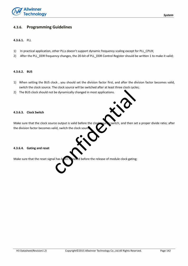
System
H3 Datasheet(Revision1.2) Copyright© 2015 Allwinner Technology Co.,Ltd.All Rights Reserved. Page 142
4.3.6. Programming Guidelines
4.3.6.1. PLL
1) In practical application, other PLLs doesn’t support dynamic frequency scaling except for PLL_CPUX;
2) After the PLL_DDR frequency changes, the 20-bit of PLL_DDR Control Register should be written 1 to make it valid;
4.3.6.2. BUS
1) When setting the BUS clock , you should set the division factor first, and after the division factor becomes valid,
switch the clock source. The clock source will be switched after at least three clock cycles;
2) The BUS clock should not be dynamically changed in most applications.
4.3.6.3. Clock Switch
Make sure that the clock source output is valid before the clock source switch, and then set a proper divide ratio; after
the division factor becomes valid, switch the clock source.
4.3.6.4. Gating and reset
Make sure that the reset signal has been released before the release of module clock gating;
confid
ential
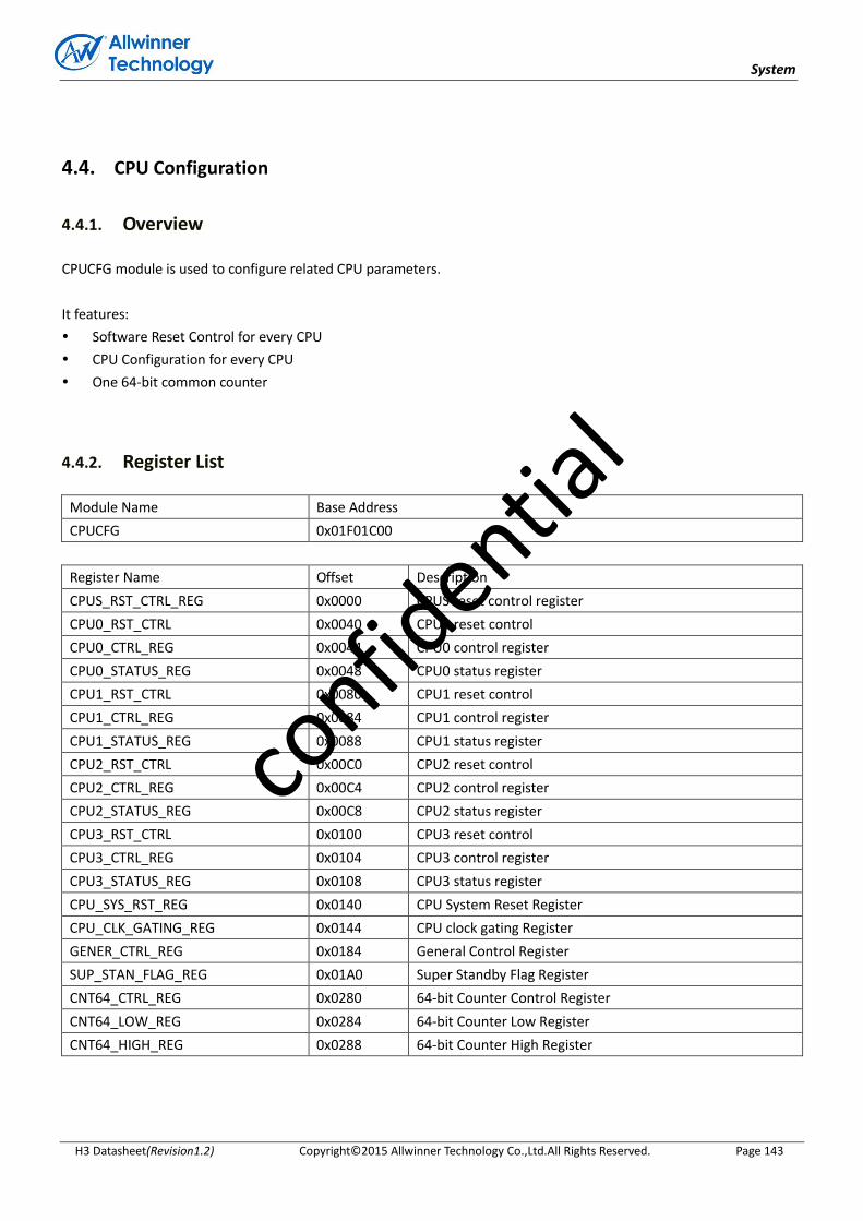
System
H3 Datasheet(Revision1.2) Copyright© 2015 Allwinner Technology Co.,Ltd.All Rights Reserved. Page 143
4.4. CPU Configuration
4.4.1. Overview
CPUCFG module is used to configure related CPU parameters.
It features:
Software Reset Control for every CPU
CPU Configuration for every CPU
One 64-bit common counter
4.4.2. Register List
Module Name Base Address
CPUCFG 0x01F01C00
Register Name Offset Description
CPUS_RST_CTRL_REG 0x0000 CPUS reset control register
CPU0_RST_CTRL 0x0040 CPU0 reset control
CPU0_CTRL_REG 0x0044 CPU0 control register
CPU0_STATUS_REG 0x0048 CPU0 status register
CPU1_RST_CTRL 0x0080 CPU1 reset control
CPU1_CTRL_REG 0x0084 CPU1 control register
CPU1_STATUS_REG 0x0088 CPU1 status register
CPU2_RST_CTRL 0x00C0 CPU2 reset control
CPU2_CTRL_REG 0x00C4 CPU2 control register
CPU2_STATUS_REG 0x00C8 CPU2 status register
CPU3_RST_CTRL 0x0100 CPU3 reset control
CPU3_CTRL_REG 0x0104 CPU3 control register
CPU3_STATUS_REG 0x0108 CPU3 status register
CPU_SYS_RST_REG 0x0140 CPU System Reset Register
CPU_CLK_GATING_REG 0x0144 CPU clock gating Register
GENER_CTRL_REG 0x0184 General Control Register
SUP_STAN_FLAG_REG 0x01A0 Super Standby Flag Register
CNT64_CTRL_REG 0x0280 64-bit Counter Control Register
CNT64_LOW_REG 0x0284 64-bit Counter Low Register
CNT64_HIGH_REG 0x0288 64-bit Counter High Register
confid
ential
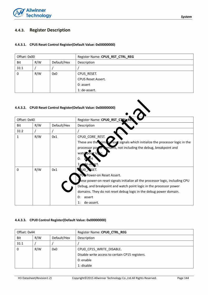
System
H3 Datasheet(Revision1.2) Copyright© 2015 Allwinner Technology Co.,Ltd.All Rights Reserved. Page 144
4.4.3. Register Description
4.4.3.1. CPUS Reset Control Register(Default Value: 0x00000000)
Offset: 0x00 Register Name: CPUS_RST_CTRL_REG
Bit R/W Default/Hex Description
31:1 / / /
0 R/W 0x0 CPUS_RESET.
CPUS Reset Assert.
0: assert
1: de-assert.
4.4.3.2. CPU0 Reset Control Register(Default Value: 0x00000000)
Offset: 0x40 Register Name: CPU0_RST_CTRL_REG
Bit R/W Default/Hex Description
31:2 / / /
1 R/W 0x1 CPU0_CORE_REST.
These are the primary reset signals which initialize the processor logic in the
processor power domains, not including the debug, breakpoint and
watchpoint logic.
0: assert
1: de-assert.
0 R/W 0x1 CPU0_RESET.
CPU0 Power-on Reset Assert.
These power-on reset signals initialize all the processor logic, including CPU
Debug, and breakpoint and watch point logic in the processor power
domains. They do not reset debug logic in the debug power domain.
0: assert
1: de-assert.
4.4.3.3. CPU0 Control Register(Default Value: 0x00000000)
Offset: 0x44 Register Name: CPU0_CTRL_REG
Bit R/W Default/Hex Description
31:1 / / /
0 R/W 0x0 CPU0_CP15_WRITE_DISABLE.
Disable write access to certain CP15 registers.
0: enable
1: disable
confid
ential

System
H3 Datasheet(Revision1.2) Copyright© 2015 Allwinner Technology Co.,Ltd.All Rights Reserved. Page 145
4.4.3.4. CPU0 Status Register (Default Value: 0x00000000)
Offset: 0x48 Register Name: CPU0_STATUS_REG
Bit R/W Default/Hex Description
31:3 / / /
2 R 0x0 STANDBYWFI.
Indicates if the processor is in WFI standby mode:
0: Processor not in WFI standby mode.
1: Processor in WFI standby mode
1 R 0x0 STANDBYWFE.
Indicates if the processor is in the WFE standby mode:
0: Processor not in WFE standby mode
1: Processor in WFE standby mode
0 R 0x0 SMP_AMP
0: AMP mode
1: SMP mode
4.4.3.5. CPU1 Reset Register(Default Value: 0x00000001)
Offset: 0x80 Register Name: CPU1_RST_CTRL_REG
Bit R/W Default/Hex Description
31:2 / / /
1 R/W 0x0 CPU1_CORE_REST.
These are the primary reset signals which initialize the processor logic in the
processor power domains, not including the debug, breakpoint and
watchpoint logic.
0: assert
1: de-assert.
0 R/W 0x1 CPU1_RESET.
CPU1 Power-on Reset Assert.
These power-on reset signals initialize all the processor logic, including CPU
Debug, and breakpoint and watch point logic in the processor power
domains. They do not reset debug logic in the debug power domain.
0: assert
1: de-assert.
4.4.3.6. CPU1 Control Register(Default Value: 0x00000000)
Offset: 0x84 Register Name: CPU1_CTRL_REG
Bit R/W Default/Hex Description
31:1 / / /
0 R/W 0x0 CPU1_CP15_WRITE_DISABLE.
confid
ential
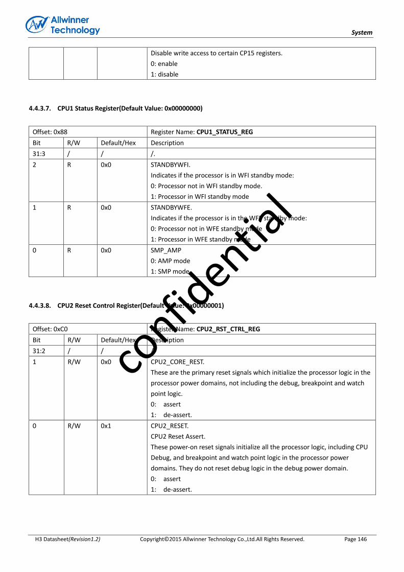
System
H3 Datasheet(Revision1.2) Copyright© 2015 Allwinner Technology Co.,Ltd.All Rights Reserved. Page 146
Disable write access to certain CP15 registers.
0: enable
1: disable
4.4.3.7. CPU1 Status Register(Default Value: 0x00000000)
Offset: 0x88 Register Name: CPU1_STATUS_REG
Bit R/W Default/Hex Description
31:3 / / /.
2 R 0x0 STANDBYWFI.
Indicates if the processor is in WFI standby mode:
0: Processor not in WFI standby mode.
1: Processor in WFI standby mode
1 R 0x0 STANDBYWFE.
Indicates if the processor is in the WFE standby mode:
0: Processor not in WFE standby mode
1: Processor in WFE standby mode
0 R 0x0 SMP_AMP
0: AMP mode
1: SMP mode
4.4.3.8. CPU2 Reset Control Register(Default Value: 0x00000001)
Offset: 0xC0 Register Name: CPU2_RST_CTRL_REG
Bit R/W Default/Hex Description
31:2 / / /.
1 R/W 0x0 CPU2_CORE_REST.
These are the primary reset signals which initialize the processor logic in the
processor power domains, not including the debug, breakpoint and watch
point logic.
0: assert
1: de-assert.
0 R/W 0x1 CPU2_RESET.
CPU2 Reset Assert.
These power-on reset signals initialize all the processor logic, including CPU
Debug, and breakpoint and watch point logic in the processor power
domains. They do not reset debug logic in the debug power domain.
0: assert
1: de-assert.
confid
ential
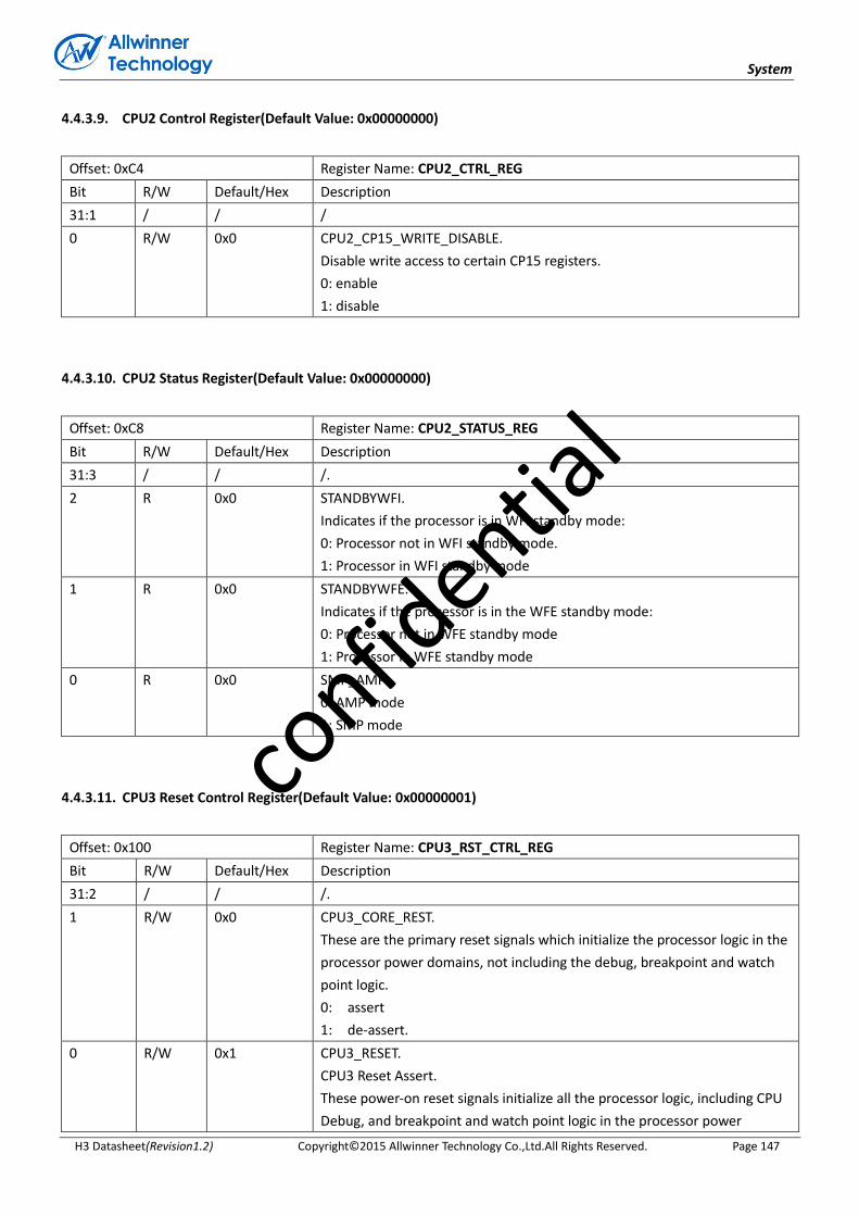
System
H3 Datasheet(Revision1.2) Copyright© 2015 Allwinner Technology Co.,Ltd.All Rights Reserved. Page 147
4.4.3.9. CPU2 Control Register(Default Value: 0x00000000)
Offset: 0xC4 Register Name: CPU2_CTRL_REG
Bit R/W Default/Hex Description
31:1 / / /
0 R/W 0x0 CPU2_CP15_WRITE_DISABLE.
Disable write access to certain CP15 registers.
0: enable
1: disable
4.4.3.10. CPU2 Status Register(Default Value: 0x00000000)
Offset: 0xC8 Register Name: CPU2_STATUS_REG
Bit R/W Default/Hex Description
31:3 / / /.
2 R 0x0 STANDBYWFI.
Indicates if the processor is in WFI standby mode:
0: Processor not in WFI standby mode.
1: Processor in WFI standby mode
1 R 0x0 STANDBYWFE.
Indicates if the processor is in the WFE standby mode:
0: Processor not in WFE standby mode
1: Processor in WFE standby mode
0 R 0x0 SMP_AMP
0: AMP mode
1: SMP mode
4.4.3.11. CPU3 Reset Control Register(Default Value: 0x00000001)
Offset: 0x100 Register Name: CPU3_RST_CTRL_REG
Bit R/W Default/Hex Description
31:2 / / /.
1 R/W 0x0 CPU3_CORE_REST.
These are the primary reset signals which initialize the processor logic in the
processor power domains, not including the debug, breakpoint and watch
point logic.
0: assert
1: de-assert.
0 R/W 0x1 CPU3_RESET.
CPU3 Reset Assert.
These power-on reset signals initialize all the processor logic, including CPU
Debug, and breakpoint and watch point logic in the processor power
confid
ential

System
H3 Datasheet(Revision1.2) Copyright© 2015 Allwinner Technology Co.,Ltd.All Rights Reserved. Page 148
domains. They do not reset debug logic in the debug power domain.
0: assert
1: de-assert.
4.4.3.12. CPU3 Control Register(Default Value: 0x00000000)
Offset: 0x104 Register Name: CPU3_CTRL_REG
Bit R/W Default/Hex Description
31:1 / / /
0 R/W 0x0 CPU3_CP15_WRITE_DISABLE.
Disable write access to certain CP15 registers.
0: enable
1: disable
4.4.3.13. CPU3 Status Register(Default Value: 0x00000000)
Offset: 0x108 Register Name: CPU3_STATUS_REG
Bit R/W Default/Hex Description
31:3 / / /.
2 R 0x0 STANDBYWFI.
Indicates if the processor is in WFI standby mode:
0: Processor not in WFI standby mode.
1: Processor in WFI standby mode
1 R 0x0 STANDBYWFE.
Indicates if the processor is in the WFE standby mode:
0: Processor not in WFE standby mode
1: Processor in WFE standby mode
0 R 0x0 SMP_AMP
0: AMP mode
1: SMP mode
4.4.3.14. CPU System Reset Control Register(Default Value: 0x00000001)
Offset: 0x140 Register Name: CPU_SYS_RST_REG
Bit R/W Default/Hex Description
31:1 / / /
0 R/W 0x1 CPU System Reset Control.
0: assert
1: de-assert.
confid
ential

System
H3 Datasheet(Revision1.2) Copyright© 2015 Allwinner Technology Co.,Ltd.All Rights Reserved. Page 149
4.4.3.15. CPU Clock Gating Register(Default Value: 0x0000010F)
Offset: 0x144 Register Name: CPU_CLK_GATING_REG
Bit R/W Default/Hex Description
31:9 / / /
8 R/W 0x1 L2_CLK_GATING
L2 Clock gating
0: clock off
1: clock on
7:4 / / /
3:0 R/W 0xF CPU_CLK_GATING
CPU0/1/2/3 Clock gating
0: clock off
1: clock on
4.4.3.16. General Control Register(Default Value: 0x00000020)
Offset: 0x184 Register Name: GENER_CTRL_REG
Bit R/W Default/Hex Description
31:9 / / /.
8 R/W 0x0 CFGSDISABLE.
Disables write access to some secure GIC registers.
7 / / /
6 R/W 0x0 ACINACTM.
Snoop interface is inactive and no longer accepting requests.
5 R/W 0x1 L2_RST.
L2 Reset.(SCU global reset)
0: Apply reset to shared L2 memory system controller.
1: Do not apply reset to shared L2 memory system controller.
4 R/W 0x0 L2_RST_DISABLE.
Disable automatic L2 cache invalidate at reset:
0: L2 cache is reset by hardware.
1: L2 cache is not reset by hardware.
3:0 R/W 0x0 L1_RST_DISABLE.
L1 Reset Disable[3:0].
0: L1 cache is reset by hardware.
1: L1 cache is not reset by hardware.
4.4.3.17. Super Standby Flag Register(Default Value: 0x00000000)
Offset: 0x1A0 Register Name: SUP_STAN_FLAG_REG
Bit R/W Default/Hex Description
confid
ential

System
H3 Datasheet(Revision1.2) Copyright© 2015 Allwinner Technology Co.,Ltd.All Rights Reserved. Page 150
31:16 R/W 0x0 SUP_STANDBY_FLAG.
Key Field.
Any value can be written and read back in the key field, but if the values are
not appropriate, the lower 16 bits will not change in this register. Only fellow
the appropriate process, the super standby flag can be written in the lower
16 bits. Refer to Description and Diagram.
15:0 R/W 0x0 SUP_STANBY_FLAG_DATA.
Refer to Description and Diagram
Note: When system is turned on, the value in the Super Standby Flag Register low 16 bits should be 0x0. If software
programmer wants to write correct super standby flag ID in low 16 bits, the high 16 bits should be written 0x16AA at
first. Then, software programmer must write 0xAA16XXXX in the Super Standby Flag Register, the ‘XXXX’ means the
correct super standby flag ID. Referring to the Diagram section (Diagram 1.1) in detail.
4.4.3.18. 64-bit Counter Control Register(Default Value: 0x00000000)
Offset: 0x280 Register Name: CNT64_CTRL_REG
Bit R/W Default/Hex Description
31:3 / / /.
2 R/W 0x0 CNT64_CLK_SRC_SEL.
64-bit Counter Clock Source Select.
0: OSC24M
1: /
1 R/W 0x0 CNT64_RL_EN.
64-bit Counter Read Latch Enable.
0: no effect, 1: to latch the 64-bit Counter to the Low/Hi registers and it will
change to zero after the registers are latched.
0 R/W 0x0 CNT64_CLR_EN.
64-bit Counter Clear Enable.
0: no effect, 1: to clear the 64-bit Counter Low/Hi registers and it will change
to zero after the registers are cleared.
Note: It is not recommended to clear this counter arbitrarily.
Note: This 64-bit counter will start to count as soon as the System Power On finished.
4.4.3.19. 64-bit Counter Low Register(Default Value: 0x00000000)
Offset: 0x284 Register Name: CNT64_LOW_REG
Bit R/W Default/Hex Description
31:0 R/W 0x0 CNT64_LO.
64-bit Counter [31:0].
confid
ential
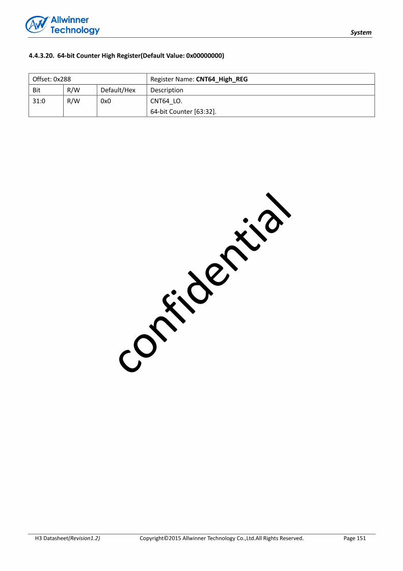
System
H3 Datasheet(Revision1.2) Copyright© 2015 Allwinner Technology Co.,Ltd.All Rights Reserved. Page 151
4.4.3.20. 64-bit Counter High Register(Default Value: 0x00000000)
Offset: 0x288 Register Name: CNT64_High_REG
Bit R/W Default/Hex Description
31:0 R/W 0x0 CNT64_LO.
64-bit Counter [63:32].
confid
ential

System
H3 Datasheet(Revision1.2) Copyright© 2015 Allwinner Technology Co.,Ltd.All Rights Reserved. Page 152
4.5. System Control
4.5.1. Overview
Area Size(Bytes)
A1 64K
A2 32K
CPUX I-Cache 32K (X=0,1,2,3)
CPUX D-Cache 32K (X=0,1,2,3)
CPU L2 Cache 512K
Total 864K
4.5.2. System Control Register List
Module Name Base Address
System Control 0x01C00000
Register Name Offset Description
VER_REG 0x24 Version Register
EMAC_EPHY_CLK_REG 0x30 EMAC-EPHY Clock Register
4.5.3. System Control Register Description
4.5.3.1. Version Register
Offset:0x24 Register Name: VER_REG
Bit R/W Default/Hex Description
31:9 / / /
8 R x UBOOT_SEL_PAD_STA.
U_boot Select Pin Status.
0: U_Boot;
1: Normal Boot.
7:0 R 0x0 VER_BITS.
This read-only bit field always reads back the mask revision level of the
chip.
confid
ential

System
H3 Datasheet(Revision1.2) Copyright© 2015 Allwinner Technology Co.,Ltd.All Rights Reserved. Page 153
4.5.3.2. EMAC Clock Register (Default Value: 0x00058000)
Offset:0x30 Register Name: EMAC_CLK_REG
Bit R/W Default/Hex Description
31:28 R/W 0x0 BPS_EFFUSE
27 R/W 0x0 XMII_SEL
0: Internal SMI and MII
1: External SMI and MII
26:25 R/W 0x0 EPHY_MODE
Operation Mode Selection
00 : Normal Mode
01 : Sim Mode
10 : AFE Test Mode
11 : /
24:20 R/W 0x0 PHY_ADDR
PHY Address
19 R/W 0x0 BIST_CLK_EN
0 : BIST clk disable
1 : BIST clk enable
18 R/W 0x1 CLK_SEL
0 : 25MHz
1 : 24MHz
17 R/W 0x0 LED_POL
0 : High active
1 : Low active
16 R/W 0x1 SHUTDOWN
0 : Power up
1 : Shutdown
15 R/W 0x1 PHY_SELECT.
0 : External PHY
1 : Internal PHY
14 / / /
13 R/W 0x0 RMII_EN
0 : Disable RMII Module
1 : Enable RMII Module
When this bit assert, MII or RGMII interface is disabled( This means bit13 is
prior to bit2)
12:10 R/W 0x0 ETXDC.
Configure EMAC Transmit Clock Delay Chain.
9:5 R/W 0x0 ERXDC.
Configure EMAC Receive Clock Delay Chain.
4 R/W 0x0 ERXIE
Enable EMAC Receive Clock Invertor.
0: Disable
confid
ential

System
H3 Datasheet(Revision1.2) Copyright© 2015 Allwinner Technology Co.,Ltd.All Rights Reserved. Page 154
1: Enable
3 R/W 0x0 ETXIE
Enable EMAC Transmit Clock Invertor.
0: Disable
1: Enable
2 R/W 0x0 EPIT
EMAC PHY Interface Type
0: MII
1: RGMII
1:0 R/W 0x0 ETCS.
EMAC Transmit Clock Source
00: Transmit clock source for MII
01: External transmit clock source for GMII and RGMII
10: Internal transmit clock source for GMII and RGMII
11: Reserved
confid
ential
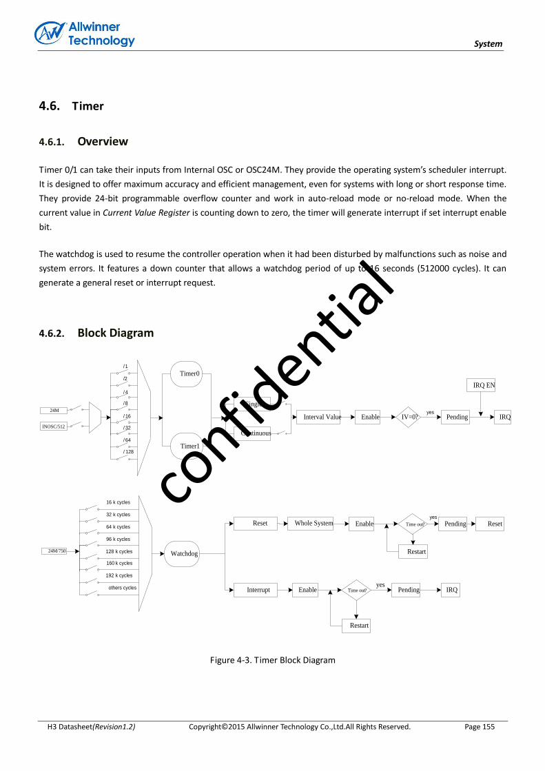
System
H3 Datasheet(Revision1.2) Copyright© 2015 Allwinner Technology Co.,Ltd.All Rights Reserved. Page 155
4.6. Timer
4.6.1. Overview
Timer 0/1 can take their inputs from Internal OSC or OSC24M. They provide the operating system’s scheduler interrupt.
It is designed to offer maximum accuracy and efficient management, even for systems with long or short response time.
They provide 24-bit programmable overflow counter and work in auto-reload mode or no-reload mode. When the
current value in Current Value Register is counting down to zero, the timer will generate interrupt if set interrupt enable
bit.
The watchdog is used to resume the controller operation when it had been disturbed by malfunctions such as noise and
system errors. It features a down counter that allows a watchdog period of up to 16 seconds (512000 cycles). It can
generate a general reset or interrupt request.
4.6.2. Block Diagram
24M
INOSC/512
Timer 0
Timer 1
Single
Continuous
Interval Value Enable IV=0? Pending
IRQ EN
IRQyes
/1
/2
/4
/8
/ 16
/ 32
/ 64
/ 128
Watchdog
Interrupt Enable Pending IRQ
16 k cycles
32 k cycles
64 k cycles
96 k cycles
128 k cycles
160 k cycles
192 k cycles
others cycles
24M/750
Restart
Time out? yes
Reset Enable Pending
Restart
Whole System Resetyes
Time out?
Figure 4-3. Timer Block Diagram
confid
ential

System
H3 Datasheet(Revision1.2) Copyright© 2015 Allwinner Technology Co.,Ltd.All Rights Reserved. Page 156
4.6.3. Timer Register List
Module Name Base Address
TIMER 0x01C20C00
Register Name Offset Description
TMR_IRQ_EN_REG 0x0 Timer IRQ Enable Register
TMR_IRQ_STA_REG 0x4 Timer Status Register
TMR0_CTRL_REG 0x10 Timer 0 Control Register
TMR0_INTV_VALUE_REG 0x14 Timer 0 Interval Value Register
TMR0_CUR_VALUE_REG 0x18 Timer 0 Current Value Register
TMR1_CTRL_REG 0x20 Timer 1 Control Register
TMR1_INTV_VALUE_REG 0x24 Timer 1 Interval Value Register
TMR1_CUR_VALUE_REG 0x28 Timer 1 Current Value Register
AVS_CNT_CTL_REG 0x80 AVS Control Register
AVS_CNT0_REG 0x84 AVS Counter 0 Register
AVS_CNT1_REG 0x88 AVS Counter 1 Register
AVS_CNT_DIV_REG 0x8C AVS Divisor Register
WDOG0_IRQ_EN_REG 0xA0 Watchdog 0 IRQ Enable Register
WDOG0_IRQ_STA_REG 0xA4 Watchdog 0 Status Register
WDOG0_CTRL_REG 0xB0 Watchdog 0 Control Register
WDOG0_CFG_REG 0xB4 Watchdog 0 Configuration Register
WDOG0_MODE_REG 0xB8 Watchdog 0 Mode Register
4.6.4. Timer Register Description
4.6.4.1. Timer IRQ Enable Register (Default Value: 0x00000000)
Offset:0x0 Register Name: TMR_IRQ_EN_REG
Bit R/W Default/Hex Description
31:2 / / /
1 R/W 0x0 TMR1_IRQ_EN.
Timer 1 Interrupt Enable.
0: No effect;
1: Timer 1 Interval Value reached interrupt enable.
0 R/W 0x0 TMR0_IRQ_EN.
Timer 0 Interrupt Enable.
0: No effect;
1: Timer 0 Interval Value reached interrupt enable.
confid
ential
System
H3 Datasheet(Revision1.2) Copyright© 2015 Allwinner Technology Co.,Ltd.All Rights Reserved. Page 157
4.6.4.2. Timer IRQ Status Register (Default Value: 0x00000000)
Offset:0x04 Register Name: TMR_IRQ_STA_REG
Bit R/W Default/Hex Description
31:2 / / /
1 R/W 0x0 TMR1_IRQ_PEND.
Timer 1 IRQ Pending. Set 1 to the bit will clear it.
0: No effect;
1: Pending, timer 1 interval value is reached.
0 R/W 0x0 TMR0_IRQ_PEND.
Timer 0 IRQ Pending. Set 1 to the bit will clear it.
0: No effect;
1: Pending, timer 0 interval value is reached.
4.6.4.3. Timer 0 Control Register (Default Value: 0x00000004)
Offset:0x10 Register Name: TMR0_CTRL_REG
Bit R/W Default/Hex Description
31:8 / / /
7 R/W 0x0 TMR0_MODE.
Timer 0 mode.
0: Continuous mode. When interval value reached, the timer will not
disable automatically.
1: Single mode. When interval value reached, the timer will disable
automatically.
6:4 R/W 0x0 TMR0_CLK_PRES.
Select the pre-scale of timer 0 clock source.
000: /1
001: /2
010: /4
011: /8
100: /16
101: /32
110: /64
111: /128
3:2 R/W 0x1 TMR0_CLK_SRC.
Timer 0 Clock Source.
00: Internal OSC / N
01: OSC24M.
10: /
11: /
Internal OSC / N is about 32KHz.
1 R/W 0x0 TMR0_RELOAD.
confid
ential
System
H3 Datasheet(Revision1.2) Copyright© 2015 Allwinner Technology Co.,Ltd.All Rights Reserved. Page 158
Timer 0 Reload.
0: No effect
1: Reload timer 0 Interval value.
After the bit is set, it can not be written again before it’s cleared
automatically.
0 R/W 0x0 TMR0_EN.
Timer 0 Enable.
0: Stop/Pause
1: Start.
When the timer is started, it will reload the interval value to internal
register, and the current counter will count from interval value to 0. If the
current counter does not reach the zero, the timer enable bit is set to “0”,
the current value counter will pause. At least wait for 2 cycles, the start bit
can be set to 1.In timer pause state; the interval value register can be
modified. If the timer is started again, and the Software hope the current
value register to down-count from the new interval value, the reload bit
and the enable bit should be set to 1 at the same time.
4.6.4.4. Timer 0 Interval Value Register
Offset:0x14 Register Name: TMR0_INTV_VALUE_REG
Bit R/W Default/Hex Description
31:0 R/W 0x0 TMR0_INTV_VALUE.
Timer 0 Interval Value.
Note:The value setting should consider the system clock and the timer clock source.
4.6.4.5. Timer 0 Current Value Register
Offset:0x18 Register Name: TMR0_CUR_VALUE_REG
Bit R/W Default/Hex Description
31:0 R/W 0x0 TMR0_CUR_VALUE.
Timer 0 Current Value.
Note: Timer0 current value is a 32-bit down-counter (from interval value to 0).
4.6.4.6. Timer 1 Control Register (Default Value: 0x00000004)
Offset:0x20 Register Name: TMR1_CTRL_REG
Bit R/W Default/Hex Description
31:8 / / /
7 R/W 0x0 TMR1_MODE.
Timer 1 mode.
0: Continuous mode. When interval value reached, the timer will not disable
confid
ential

System
H3 Datasheet(Revision1.2) Copyright© 2015 Allwinner Technology Co.,Ltd.All Rights Reserved. Page 159
automatically.
1: Single mode. When interval value reached, the timer will disable
automatically.
6:4 R/W 0x0 TMR1_CLK_PRES.
Select the pre-scale of timer 1 clock source.
000: /1
001: /2
010: /4
011: /8
100: /16
101: /32
110: /64
111: /128
3:2 R/W 0x1 TMR1_CLK_SRC.
00: Internal OSC / N
01: OSC24M.
10: /
11: /.
Internal OSC / N is about 32KHz.
1 R/W 0x0 TMR1_RELOAD.
Timer 1 Reload.
0: No effect
1: Reload timer 1 Interval value.
After the bit is set, it can not be written again before it’s cleared
automatically.
0 R/W 0x0 TMR1_EN.
Timer 1 Enable.
0: Stop/Pause
1: Start.
If the timer is started, it will reload the interval value to internal register, and
the current counter will count from interval value to 0.
If the current counter does not reach the zero, the timer enable bit is set to
“0”, the current value counter will pause. At least wait for 2 cycles, the start
bit can be set to 1.
In timer pause state, the interval value register can be modified. If the timer
is started again, and the Software hope the current value register to
down-count from the new interval value, the reload bit and the enable bit
should be set to 1 at the same time.
4.6.4.7. Timer 1 Interval Value Register
Offset:0x24 Register Name: TMR1_INTV_VALUE_REG
Bit R/W Default/Hex Description
31:0 R/W 0x0 TMR1_INTV_VALUE.
confid
ential
System
H3 Datasheet(Revision1.2) Copyright© 2015 Allwinner Technology Co.,Ltd.All Rights Reserved. Page 160
Timer 1 Interval Value.
Note: The value setting should consider the system clock and the timer clock source.
4.6.4.8. Timer 1 Current Value Register
Offset:0x28 Register Name: TMR1_CUR_VALUE_REG
Bit R/W Default/Hex Description
31:0 R/W 0x0 TMR1_CUR_VALUE.
Timer 1 Current Value.
Note: Timer1 current value is a 32-bit down-counter (from interval value to 0).
4.6.4.9. AVS Counter Control Register (Default Value: 0x00000000)
Offset:0x80 Register Name: AVS_CNT_CTL_REG
Bit R/W Default/Hex Description
31:10 / / /
9 R/W 0x0 AVS_CNT1_PS.
Audio/Video Sync Counter 1 Pause Control
0: Not pause
1: Pause Counter 1.
8 R/W 0x0 AVS_CNT0_PS.
Audio/Video Sync Counter 0 Pause Control
0: Not pause
1: Pause Counter 0.
7:2 / / /
1 R/W 0x0 AVS_CNT1_EN.
Audio/Video Sync Counter 1 Enable/ Disable. The counter source is OSC24M.
0: Disable
1: Enable.
0 R/W 0x0 AVS_CNT0_EN.
Audio/Video Sync Counter 1 Enable/ Disable. The counter source is OSC24M.
0: Disable
1: Enable.
4.6.4.10. AVS Counter 0 Register (Default Value: 0x00000000)
Offset:0x84 Register Name: AVS_CNT0_REG
Bit R/W Default/Hex Description
31:0 R/W 0x0 AVS_CNT0.
Counter 0 for Audio/ Video Sync Application
The high 32 bits of the internal 33-bits counter register. The initial value of
confid
ential
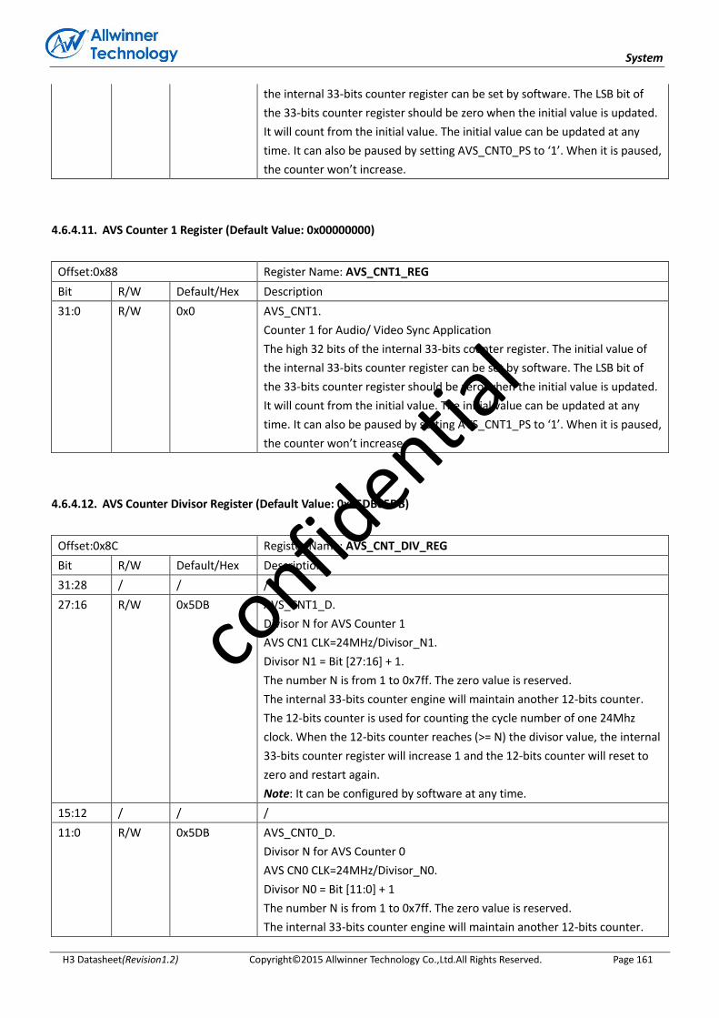
System
H3 Datasheet(Revision1.2) Copyright© 2015 Allwinner Technology Co.,Ltd.All Rights Reserved. Page 161
the internal 33-bits counter register can be set by software. The LSB bit of
the 33-bits counter register should be zero when the initial value is updated.
It will count from the initial value. The initial value can be updated at any
time. It can also be paused by setting AVS_CNT0_PS to ‘1’. When it is paused,
the counter won’t increase.
4.6.4.11. AVS Counter 1 Register (Default Value: 0x00000000)
Offset:0x88 Register Name: AVS_CNT1_REG
Bit R/W Default/Hex Description
31:0 R/W 0x0 AVS_CNT1.
Counter 1 for Audio/ Video Sync Application
The high 32 bits of the internal 33-bits counter register. The initial value of
the internal 33-bits counter register can be set by software. The LSB bit of
the 33-bits counter register should be zero when the initial value is updated.
It will count from the initial value. The initial value can be updated at any
time. It can also be paused by setting AVS_CNT1_PS to ‘1’. When it is paused,
the counter won’t increase.
4.6.4.12. AVS Counter Divisor Register (Default Value: 0x05DB05DB)
Offset:0x8C Register Name: AVS_CNT_DIV_REG
Bit R/W Default/Hex Description
31:28 / / /
27:16 R/W 0x5DB AVS_CNT1_D.
Divisor N for AVS Counter 1
AVS CN1 CLK=24MHz/Divisor_N1.
Divisor N1 = Bit [27:16] + 1.
The number N is from 1 to 0x7ff. The zero value is reserved.
The internal 33-bits counter engine will maintain another 12-bits counter.
The 12-bits counter is used for counting the cycle number of one 24Mhz
clock. When the 12-bits counter reaches (>= N) the divisor value, the internal
33-bits counter register will increase 1 and the 12-bits counter will reset to
zero and restart again.
Note: It can be configured by software at any time.
15:12 / / /
11:0 R/W 0x5DB AVS_CNT0_D.
Divisor N for AVS Counter 0
AVS CN0 CLK=24MHz/Divisor_N0.
Divisor N0 = Bit [11:0] + 1
The number N is from 1 to 0x7ff. The zero value is reserved.
The internal 33-bits counter engine will maintain another 12-bits counter.
confid
ential
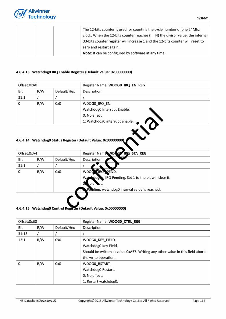
System
H3 Datasheet(Revision1.2) Copyright© 2015 Allwinner Technology Co.,Ltd.All Rights Reserved. Page 162
The 12-bits counter is used for counting the cycle number of one 24Mhz
clock. When the 12-bits counter reaches (>= N) the divisor value, the internal
33-bits counter register will increase 1 and the 12-bits counter will reset to
zero and restart again.
Note: It can be configured by software at any time.
4.6.4.13. Watchdog0 IRQ Enable Register (Default Value: 0x00000000)
Offset:0xA0 Register Name: WDOG0_IRQ_EN_REG
Bit R/W Default/Hex Description
31:1 / / /
0 R/W 0x0 WDOG0_IRQ_EN.
Watchdog0 Interrupt Enable.
0: No effect
1: Watchdog0 interrupt enable.
4.6.4.14. Watchdog0 Status Register (Default Value: 0x00000000)
Offset:0xA4 Register Name: WDOG0_IRQ_STA_REG
Bit R/W Default/Hex Description
31:1 / / /
0 R/W 0x0 WDOG0_IRQ _PEND.
Watchdog0 n IRQ Pending. Set 1 to the bit will clear it.
0: No effect,
1: Pending, watchdog0 interval value is reached.
4.6.4.15. Watchdog0 Control Register (Default Value: 0x00000000)
Offset:0xB0 Register Name: WDOG0_CTRL_REG
Bit R/W Default/Hex Description
31:13 / / /
12:1 R/W 0x0 WDOG0_KEY_FIELD.
Watchdog0 Key Field.
Should be written at value 0xA57. Writing any other value in this field aborts
the write operation.
0 R/W 0x0 WDOG0_RSTART.
Watchdog0 Restart.
0: No effect,
1: Restart watchdog0.
confid
ential

System
H3 Datasheet(Revision1.2) Copyright© 2015 Allwinner Technology Co.,Ltd.All Rights Reserved. Page 163
4.6.4.16. Watchdog0 Configuration Register (Default Value: 0x00000001)
Offset:0xB4 Register Name: WDOG0_CFG_REG
Bit R/W Default/Hex Description
31:2 / / /
1:0 R/W 0x1 WDOG0_CONFIG.
Watchdog0 generates a reset signal
00: /
01: To whole system
10: Only interrupt
11: /
4.6.4.17. Watchdog0 Mode Register (Default Value: 0x00000000)
Offset:0xB8 Register Name: WDOG0_MODE_REG
Bit R/W Default/Hex Description
31:8 / / /
7:4 R/W 0x0 WDOG0_INTV_VALUE.
Watchdog0 Interval Value
Watchdog0 clock source is OSC24M / 750. If the clock source is turned off,
Watchdog 0 will not work.
0000: 16000 cycles (0.5s)
0001: 32000 cycles (1s)
0010: 64000 cycles (2s)
0011: 96000 cycles (3s)
0100: 128000 cycles (4s)
0101: 160000 cycles (5s)
0110: 192000 cycles (6s)
0111: 256000 cycles (8s)
1000: 320000 cycles (10s)
1001: 384000 cycles (12s)
1010: 448000 cycles (14s)
1011: 512000 cycles (16s)
others: /
3:1 / / /
0 R/W 0x0 WDOG0_EN.
Watchdog0 Enable.
0: No effect;
1: Enable watchdog0.
confid
ential

System
H3 Datasheet(Revision1.2) Copyright© 2015 Allwinner Technology Co.,Ltd.All Rights Reserved. Page 164
4.6.5. Programming Guidelines
4.6.5.1. Timer
Take making a Timer0 1ms delay for an example, 24M clock source, single mode and 2 pre-scale will be selected in the
instance.
writel(0x2EE0,TMR_0_INTV); //Set interval value
writel(0x94, TMR_0_CTRL); //Select Single mode,24MHz clock source,2 pre-scale
writel(readl(TMR_0_CTRL)|(1<<1), TMR_0_CTRL); //Set Reload bit
while((readl(TMR_0_CTRL)>>1)&1); //Waiting Reload bit turns to 0
writel(readl(TMR_0_CTRL)|(1<<0), TMR_0_CTRL); //Enable Timer0
4.6.5.2. Watchdog Reset
In the following instance making configurations for Watchdog: configurate clock source as 24M/750, configurate Interval
Value as 1s and configurate Watchdog Configuration as To whole system. This instance indicates that reset system after
1s.
writel(0x1, WDOG_CONFIG); //To whole system
writel(0x10, WDOG_MODE); //Interval Value set 1s
writel(readl(WDOG_MODE)|(1<<0), WDOG_MODE); //Enable Watchdog
4.6.5.3. Watchdog Restart
In the following instance making configurations for Watchdog: configurate clock source as 24M/750, configurate Interval
Value as 1s and configurate Watchdog Configuration as To whole system. In the following instance, if the time of other
codes is larger than 1s, watchdog will reset the whole system. If the sentence of restart watchdog is implemented inside
1s, watchdog will be restarted.
writel(0x1, WDOG_CONFIG); //To whole system
writel(0x10, WDOG_MODE); //Interval Value set 1s
writel(readl(WDOG_MODE)|(1<<0), WDOG_MODE); //Enable Watchdog
----other codes---
writel(readl(WDOG_CTRL)|(0xA57<<1)|(1<<0),WDOG_CTRL); //Writel 0xA57 at Key Field and Restart Watchdog
confid
ential

System
H3 Datasheet(Revision1.2) Copyright© 2015 Allwinner Technology Co.,Ltd.All Rights Reserved. Page 165
4.7. Trusted Watchdog
4.7.1. Overview
The trusted watchdog is primarily used to protect the trusted world operations from denial of service when secure
services are dependent to the RichOS scheduler. For example, if the trusted world is not entered after a defined time
limit the SoC is re-started to perform an authentication of the system.
The trusted watchdog can also be used to mask the real cause of a security error thanks to the delayed warm reset it
generates.
4.7.2. Block Diagram
24M
LOSC
TWD
Interval Value
CMP Counter Value ==
Hi/Low Counter Value ?
Pending
IRQ Enable IRQ
yesCold Reset
Hi/Low Counter Rolling-over
Restart
CMP Counter Value = Hi/Low Counter Value + Interval Value
Reset Enable
Reset
Interval Value Register
Read Latch Enable
Clear Enable
Stop Enable
Clear Counter?
Read Value?
Counter Value and Interval Value are Cleared
Stop?
Hi/Low CounterStop Rolling-over
Resum?Hi/Low Counter
Continue Rolling-over
Reset Flag After Warm Reset
Figure 4-4. TWD Block Diagram
The trusted watchdog timer must always be running when the SoC wakes up from cold reset and can be refreshed,
suspended, or reset only by secure accesses. And a clock of at least 32 kHz is used when the device is not a power
saving cycles.
4.7.3. Functionalities Description
4.7.3.1. TWD Reset
The trusted watchdog timer is able to generate a SoC warm reset after a duration programmed into the timer or set by
default in hardware. And the flag indicating the occurrence of a watchdog triggered warm reset has occurred since the
last cold reset.
confid
ential
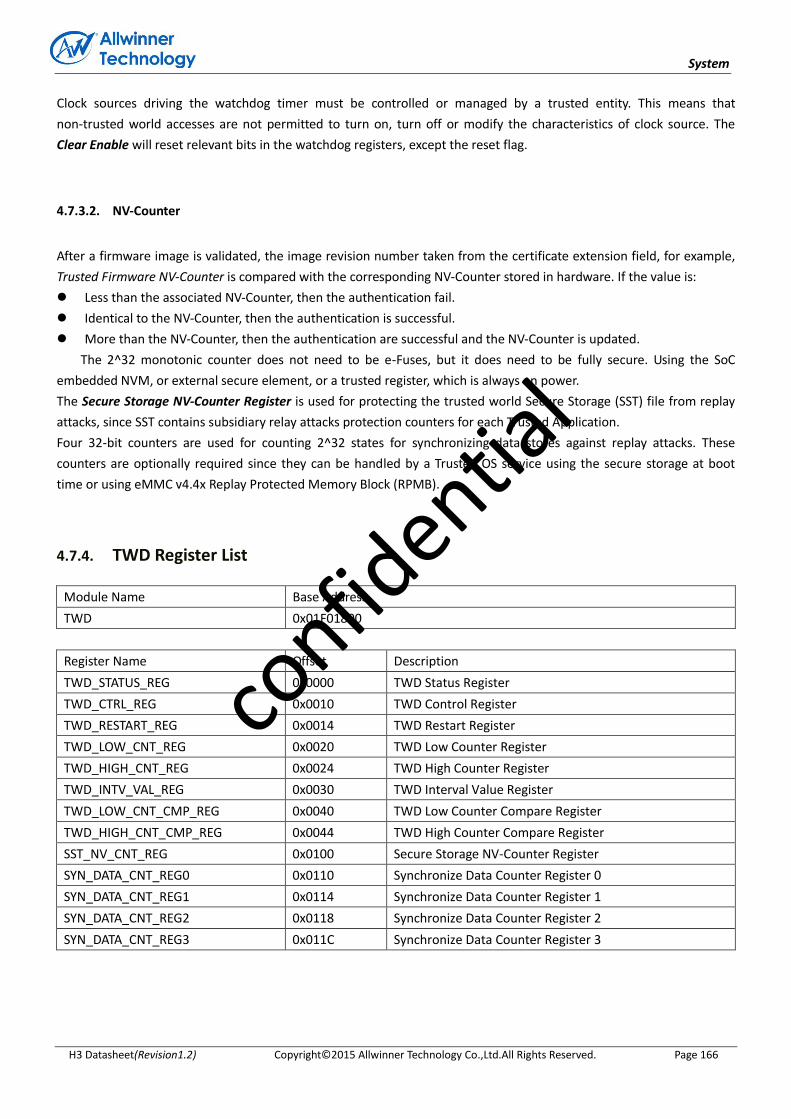
System
H3 Datasheet(Revision1.2) Copyright© 2015 Allwinner Technology Co.,Ltd.All Rights Reserved. Page 166
Clock sources driving the watchdog timer must be controlled or managed by a trusted entity. This means that
non-trusted world accesses are not permitted to turn on, turn off or modify the characteristics of clock source. The
Clear Enable will reset relevant bits in the watchdog registers, except the reset flag.
4.7.3.2. NV-Counter
After a firmware image is validated, the image revision number taken from the certificate extension field, for example,
Trusted Firmware NV-Counter is compared with the corresponding NV-Counter stored in hardware. If the value is:
Less than the associated NV-Counter, then the authentication fail.
Identical to the NV-Counter, then the authentication is successful.
More than the NV-Counter, then the authentication are successful and the NV-Counter is updated.
The 2^32 monotonic counter does not need to be e-Fuses, but it does need to be fully secure. Using the SoC
embedded NVM, or external secure element, or a trusted register, which is always on power.
The Secure Storage NV-Counter Register is used for protecting the trusted world Secure Storage (SST) file from replay
attacks, since SST contains subsidiary relay attacks protection counters for each Trusted Application.
Four 32-bit counters are used for counting 2^32 states for synchronizing data stores against replay attacks. These
counters are optionally required since they can be handled by a Trusted OS service using the secure storage at boot
time or using eMMC v4.4x Replay Protected Memory Block (RPMB).
4.7.4. TWD Register List
Module Name Base Address
TWD 0x01F01800
Register Name Offset Description
TWD_STATUS_REG 0x0000 TWD Status Register
TWD_CTRL_REG 0x0010 TWD Control Register
TWD_RESTART_REG 0x0014 TWD Restart Register
TWD_LOW_CNT_REG 0x0020 TWD Low Counter Register
TWD_HIGH_CNT_REG 0x0024 TWD High Counter Register
TWD_INTV_VAL_REG 0x0030 TWD Interval Value Register
TWD_LOW_CNT_CMP_REG 0x0040 TWD Low Counter Compare Register
TWD_HIGH_CNT_CMP_REG 0x0044 TWD High Counter Compare Register
SST_NV_CNT_REG 0x0100 Secure Storage NV-Counter Register
SYN_DATA_CNT_REG0 0x0110 Synchronize Data Counter Register 0
SYN_DATA_CNT_REG1 0x0114 Synchronize Data Counter Register 1
SYN_DATA_CNT_REG2 0x0118 Synchronize Data Counter Register 2
SYN_DATA_CNT_REG3 0x011C Synchronize Data Counter Register 3
confid
ential

System
H3 Datasheet(Revision1.2) Copyright© 2015 Allwinner Technology Co.,Ltd.All Rights Reserved. Page 167
4.7.5. TWD Register Description
4.7.5.1. TWD Status Register (Default Value: 0x00000000)
Offset: 0x0000 Register Name: TWD_STATUS_REG
Bit R/W Default/Hex Description
31:1 / / /
0 R/W 0x0 TWD_PEND_FLAG.
Interrupt pending. Set 1 to the bit will clear it.
0: No effect.
1: Pending.
4.7.5.2. TWD Control Register (Default Value: 0x00000000)
Offset: 0x0010 Register Name: TWD_CTRL_REG
Bit R/W Default/Hex Description
31 R/W 0x0 CNT64_CLK_SRC_SEL.
64-bit counter clock source select.
0: LOSC.
1: OSC24M.
30:10 / / /
9 R/W 0x0 TWD_RESET_EN.
TWD reset enable.
0: Reset disable.
1: Reset enable.
8 R/W 0x0 TWD_INT_EN.
TWD Interrupt Enable.
0: Interrupt disable.
1: Interrupt enable.
7:2 / / /
1 R/W 0x0 TWD_STOP_EN.
TWD stop enable.
0: Resume rolling-over.
1: Stop rolling-over.
0 R/W 0x0 TWD_CLR_EN.
TWD clear enable.
0: No effect.
1: To clear relevant registers and it will change to zero after the registers are
cleared.
confid
ential
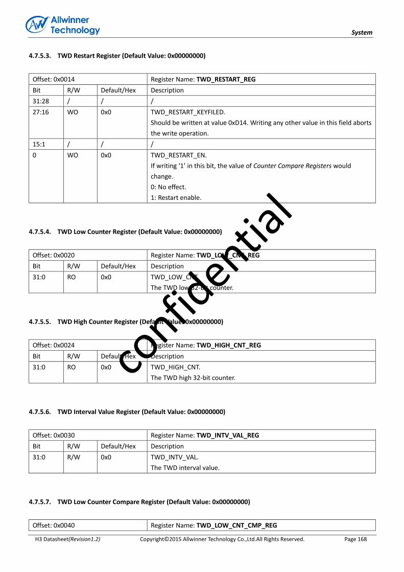
System
H3 Datasheet(Revision1.2) Copyright© 2015 Allwinner Technology Co.,Ltd.All Rights Reserved. Page 168
4.7.5.3. TWD Restart Register (Default Value: 0x00000000)
Offset: 0x0014 Register Name: TWD_RESTART_REG
Bit R/W Default/Hex Description
31:28 / / /
27:16 WO 0x0 TWD_RESTART_KEYFILED.
Should be written at value 0xD14. Writing any other value in this field aborts
the write operation.
15:1 / / /
0 WO 0x0 TWD_RESTART_EN.
If writing ‘1’ in this bit, the value of Counter Compare Registers would
change.
0: No effect.
1: Restart enable.
4.7.5.4. TWD Low Counter Register (Default Value: 0x00000000)
Offset: 0x0020 Register Name: TWD_LOW_CNT_REG
Bit R/W Default/Hex Description
31:0 RO 0x0 TWD_LOW_CNT.
The TWD low 32-bit counter.
4.7.5.5. TWD High Counter Register (Default Value: 0x00000000)
Offset: 0x0024 Register Name: TWD_HIGH_CNT_REG
Bit R/W Default/Hex Description
31:0 RO 0x0 TWD_HIGH_CNT.
The TWD high 32-bit counter.
4.7.5.6. TWD Interval Value Register (Default Value: 0x00000000)
Offset: 0x0030 Register Name: TWD_INTV_VAL_REG
Bit R/W Default/Hex Description
31:0 R/W 0x0 TWD_INTV_VAL.
The TWD interval value.
4.7.5.7. TWD Low Counter Compare Register (Default Value: 0x00000000)
Offset: 0x0040 Register Name: TWD_LOW_CNT_CMP_REG
confid
ential

System
H3 Datasheet(Revision1.2) Copyright© 2015 Allwinner Technology Co.,Ltd.All Rights Reserved. Page 169
Bit R/W Default/Hex Description
31:0 RO 0x0 TWD_LOW_CMP.
The TWD low 32-bit compare counter.
4.7.5.8. TWD High Counter Compare Register (Default Value: 0x00000000)
Offset: 0x0044 Register Name: TWD_HIGH_CNT_CMP_REG
Bit R/W Default/Hex Description
31:0 RO 0x0 TWD_HIGH_CMP.
The TWD high 32-bit compare counter.
4.7.5.9. Secure Storage NV-Counter Register (Default Value: 0x00000000)
Offset: 0x0100 Register Name: SST_NV_CNT_REG
Bit R/W Default/Hex Description
31:0 R/W 0x0 SST_NV_CNT.
This counter protects the trusted world Secure Storage file from replay
attacks.
4.7.5.10. Synchronize Data Counter Register 0 (Default Value: 0x00000000)
Offset: 0x0110 Register Name: SYN_DATA_CNT_REG0
Bit R/W Default/Hex Description
31:0 R/W 0x0 SYN_DATA_CNT0.
This counter is used for synchronizing data stores against replay attacks.
4.7.5.11. Synchronize Data Counter Register 1 (Default Value: 0x00000000)
Offset: 0x0114 Register Name: SYN_DATA_CNT_REG1
Bit R/W Default/Hex Description
31:0 R/W 0x0 SYN_DATA_CNT1.
This counter is used for synchronizing data stores against replay attacks.
4.7.5.12. Synchronize Data Counter Register 2 (Default Value: 0x00000000)
Offset: 0x0118 Register Name: SYN_DATA_CNT_REG2
Bit R/W Default/Hex Description
31:0 R/W 0x0 SYN_DATA_CNT2.
confid
ential
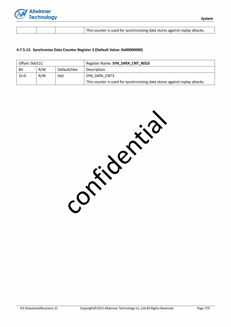
System
H3 Datasheet(Revision1.2) Copyright© 2015 Allwinner Technology Co.,Ltd.All Rights Reserved. Page 170
This counter is used for synchronizing data stores against replay attacks.
4.7.5.13. Synchronize Data Counter Register 3 (Default Value: 0x00000000)
Offset: 0x011C Register Name: SYN_DATA_CNT_REG3
Bit R/W Default/Hex Description
31:0 R/W 0x0 SYN_DATA_CNT3.
This counter is used for synchronizing data stores against replay attacks.
confid
ential

System
H3 Datasheet(Revision1.2) Copyright© 2015 Allwinner Technology Co.,Ltd.All Rights Reserved. Page 171
4.8. RTC
4.8.1. Overview
The real time clock (RTC) is for calendar usage. It is built around a 30-bit counter and used to count elapsed time in
YY-MM-DD and HH-MM-SS. The unit can be operated by the backup battery while the system power is off. It has a
built-in leap year generator and a independent power pin (RTC_VIO).
The alarm generates an alarm signal at a specified time in the power-off mode or normal operation mode. In normal
operation mode, both the alarm interrupt and the power management wakeup are activated. In power-off mode, the
power management wakeup signal is activated. In this section, there are two kinds of alarm. Alarm 0 is a general alarm,
its counter is based on second. Alarm 1 is a weekly alarm, its counter is based on the real time.
The 32768Hz oscillator is used only to provide a low power, accurate reference for the RTC.
General Purpose Register can be flag register, and it will save the value all the time when the VDD_RTC is not power off.
4.8.2. RTC Register List
Module Name Base Address
RTC 0x01F00000
Register Name Offset Description
LOSC_CTRL_REG 0x0 Low Oscillator Control Register
LOSC_AUTO_SWT_STA_REG 0x4 LOSC Auto Switch Status Register
INTOSC_CLK_PRESCAL_REG 0x8 Internal OSC Clock Prescalar Register
RTC_YY_MM_DD_REG 0x10 RTC Year-Month-Day Register
RTC_HH_MM_SS_REG 0x14 RTC Hour-Minute-Second Register
ALARM0_COUNTER_REG 0x20 Alarm 0 Counter Register
ALARM0_CUR_VLU_REG 0x24 Alarm 0 Counter Current Value Register
ALARM0_ENABLE_REG 0x28 Alarm 0 Enable Register
ALARM0_IRQ_EN 0x2C Alarm 0 IRQ Enable Register
ALARM0_IRQ_STA_REG 0x30 Alarm 0 IRQ Status Register
ALARM1_WK_HH_MM-SS 0x40 Alarm 1 Week HMS Register
ALARM1_ENABLE_REG 0x44 Alarm 1 Enable Register
ALARM1_IRQ_EN 0x48 Alarm 1 IRQ Enable Register
ALARM1_IRQ_STA_REG 0x4C Alarm 1 IRQ Status Register
ALARM_CONFIG_REG 0x50 Alarm Config Register
LOSC_OUT_GATING_REG 0x60 LOSC output gating register
GP_DATA_REG 0x100 + N*0x4 General Purpose Register (N=0~7)
confid
ential

System
H3 Datasheet(Revision1.2) Copyright© 2015 Allwinner Technology Co.,Ltd.All Rights Reserved. Page 172
RTC_DEB_REG 0x170 RTC Debug Register
GPL_HOLD_OUTPUT_REG 0x180 GPL Hold Output Register
VDD_RTC_REG 0x190 VDD RTC Regulate Register
IC_CHARA_REG 0x1F0 IC Characteristic Register
4.8.3. RTC Register Description
4.8.3.1. LOSC Control Register (Default Value: 0x00004000)
Offset:0x0 Register Name: LOSC_CTRL_REG
Bit R/W Default/Hex Description
31:16 W 0x0 KEY_FIELD.
Key Field. This field should be filled with 0x16AA, and then the bit 0 can be
written with the new value.
15 / / /
14 R/W 0x1 LOSC_AUTO_SWT_EN.
LOSC auto switch enable.
0: Disable, 1: Enable.
13:10 / / /
9 R/W 0x0 ALM_DDHHMMSS_ACCE.
ALARM DD-HH-MM-SS access.
After writing the ALARM DD-HH-MM-SS register, this bit is set and it will be
cleared until the real writing operation is finished.
8 R/W 0x0 RTC_HHMMSS_ACCE.
RTC HH-MM-SS access.
After writing the RTC HH-MM-SS register, this bit is set and it will be cleared
until the real writing operation is finished.
After writing the RTC YY-MM-DD register, the YY-MM-DD register will be
refreshed for at most one second.
7 R/W 0x0 RTC_YYMMDD_ACCE.
RTC YY-MM-DD access.
After writing the RTC YY-MM-DD register, this bit is set and it will be cleared
until the real writing operation is finished.
After writing the RTC YY-MM-DD register, the YY-MM-DD register will be
refreshed for at most one second.
6:4 / / /
3:2 R/W 0x0 EXT_LOSC_GSM.
External 32768Hz Crystal GSM.
00 low
01
10
11 high
1 / / /
confid
ential

System
H3 Datasheet(Revision1.2) Copyright© 2015 Allwinner Technology Co.,Ltd.All Rights Reserved. Page 173
0 R/W 0x0 LOSC_SRC_SEL.
LOSC Clock source Select. ‘N’ is the value of Internal OSC Clock Prescalar
register.
0: InternalOSC /32/ N, 1: External 32.768KHz OSC.
(InternalOSC=16MHz)
Note1: Any bit of [9:7] is set, the RTC HH-MM-SS, YY-MM-DD and ALARM DD-HH-MM-SS register can’t be written.
Note2: Internal OSC is about 16MHz.
4.8.3.2. LOSC Auto Switch Status Register (Default Value: 0x00000000)
Offset:0x4 Register Name: LOSC_AUTO_SWT_STA_REG
Bit R/W Default/Hex Description
31:2 / / /
1 R/W 0x0 LOSC_AUTO_SWT_PEND.
LOSC auto switch pending.
0: No effect
1: Auto switches pending
Set 1 to this bit will clear it.
0 RO 0x0 LOSC_SRC_SEL_STA.
Checking LOSC Clock Source Status. ‘N’ is the value of Internal OSC Clock
Prescalar register.
0: InternalOSC /32/ N
1: External 32.768KHz OSC
(InternalOSC=16MHz)
4.8.3.3. Internal OSC Clock Prescalar Register (Default Value: 0x0000000F)
Offset:0x8 Register Name: INTOSC_CLK_PRESCAL_REG
Bit R/W Default/Hex Description
31:16 / / /
15:0 R/W 0xF INTOSC_CLK_PRESCAL.
Internal OSC Clock Prescalar value N.
0x000: 1
0x001: 2
0x002: 3
............
0x1F: 32
4.8.3.4. RTC YY-MM-DD Register (Default Value: 0x00000000)
Offset:0x10 Register Name: RTC_YY_MM_DD_REG
confid
ential
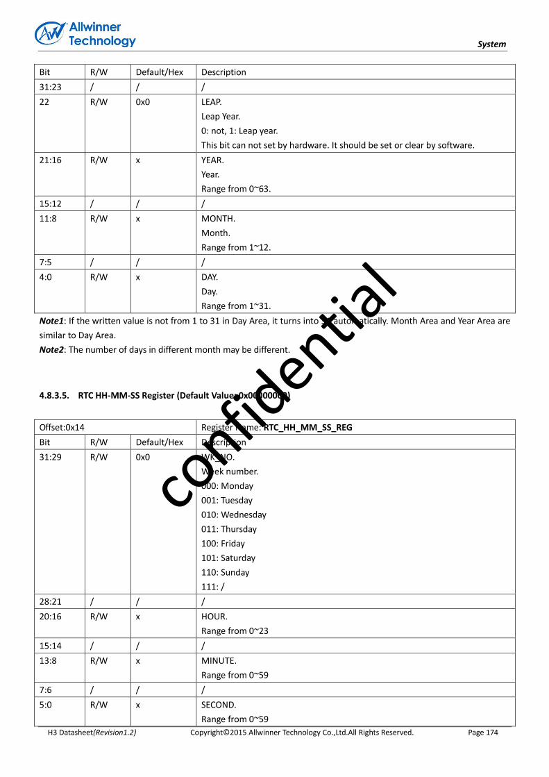
System
H3 Datasheet(Revision1.2) Copyright© 2015 Allwinner Technology Co.,Ltd.All Rights Reserved. Page 174
Bit R/W Default/Hex Description
31:23 / / /
22 R/W 0x0 LEAP.
Leap Year.
0: not, 1: Leap year.
This bit can not set by hardware. It should be set or clear by software.
21:16 R/W x YEAR.
Year.
Range from 0~63.
15:12 / / /
11:8 R/W x MONTH.
Month.
Range from 1~12.
7:5 / / /
4:0 R/W x DAY.
Day.
Range from 1~31.
Note1: If the written value is not from 1 to 31 in Day Area, it turns into 31 automatically. Month Area and Year Area are
similar to Day Area.
Note2: The number of days in different month may be different.
4.8.3.5. RTC HH-MM-SS Register (Default Value: 0x00000000)
Offset:0x14 Register Name: RTC_HH_MM_SS_REG
Bit R/W Default/Hex Description
31:29 R/W 0x0 WK_NO.
Week number.
000: Monday
001: Tuesday
010: Wednesday
011: Thursday
100: Friday
101: Saturday
110: Sunday
111: /
28:21 / / /
20:16 R/W x HOUR.
Range from 0~23
15:14 / / /
13:8 R/W x MINUTE.
Range from 0~59
7:6 / / /
5:0 R/W x SECOND.
Range from 0~59
confid
ential

System
H3 Datasheet(Revision1.2) Copyright© 2015 Allwinner Technology Co.,Ltd.All Rights Reserved. Page 175
Note: If the written value is not from 0 to 59 in Second Area, it turns into 59 automatically. Minute Area and Hour Area
are similar to Second Area.
4.8.3.6. Alarm 0 Counter Register (Default Value: 0x00000000)
Offset:0x20 Register Name: ALARM0_COUNTER_REG
Bit R/W Default/Hex Description
31:0 R/W 0x0 ALARM0_COUNTER.
Alarm 0 Counter is Based on Second.
Note: If the second is set to 0, it will be 1 second in fact.
4.8.3.7. Alarm 0 Current Value Register
Offset:0x24 Register Name: ALARM0_CUR_VLU_REG
Bit R/W Default/Hex Description
31:0 RO x ALARM0_CUR_VLU.
Check Alarm 0 Counter Current Values.
Note: If the second is set to 0, it will be 1 second in fact.
4.8.3.8. Alarm 0 Enable Register (Default Value: 0x00000000)
Offset:0x28 Register Name: ALARM0_ENABLE_REG
Bit R/W Default/Hex Description
31:1 / / /
0 R/W 0x0 ALM_0_EN
Alarm 0 Enable.
If this bit is set to “1”, the Alarm 0 Counter register’s valid bits will down count
to zero, and the alarm pending bit will be set to “1”.
0: Disable
1: Enable
4.8.3.9. Alarm 0 IRQ Enable Register (Default Value: 0x00000000)
Offset:0x2C Register Name: ALARM0_IRQ_EN
Bit R/W Default/Hex Description
31:1 / / /
0 R/W 0x0 ALARM0_IRQ_EN.
confid
ential
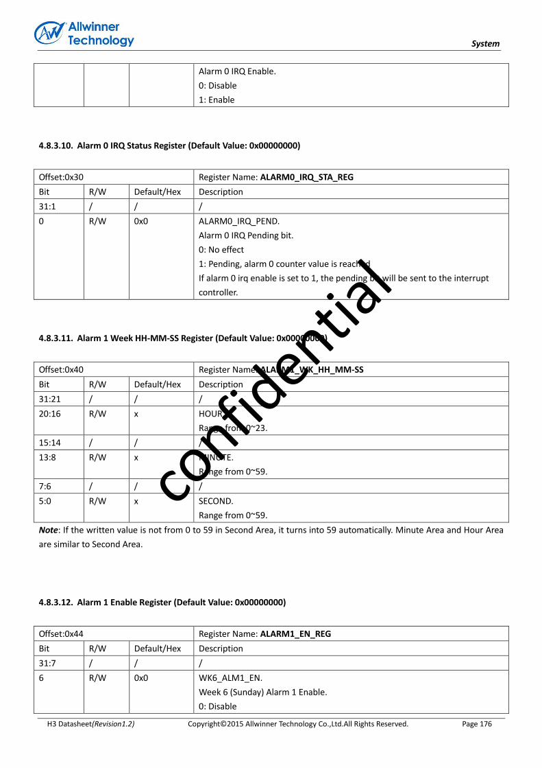
System
H3 Datasheet(Revision1.2) Copyright© 2015 Allwinner Technology Co.,Ltd.All Rights Reserved. Page 176
Alarm 0 IRQ Enable.
0: Disable
1: Enable
4.8.3.10. Alarm 0 IRQ Status Register (Default Value: 0x00000000)
Offset:0x30 Register Name: ALARM0_IRQ_STA_REG
Bit R/W Default/Hex Description
31:1 / / /
0 R/W 0x0 ALARM0_IRQ_PEND.
Alarm 0 IRQ Pending bit.
0: No effect
1: Pending, alarm 0 counter value is reached
If alarm 0 irq enable is set to 1, the pending bit will be sent to the interrupt
controller.
4.8.3.11. Alarm 1 Week HH-MM-SS Register (Default Value: 0x00000000)
Offset:0x40 Register Name: ALARM1_WK_HH_MM-SS
Bit R/W Default/Hex Description
31:21 / / /
20:16 R/W x HOUR.
Range from 0~23.
15:14 / / /
13:8 R/W x MINUTE.
Range from 0~59.
7:6 / / /
5:0 R/W x SECOND.
Range from 0~59.
Note: If the written value is not from 0 to 59 in Second Area, it turns into 59 automatically. Minute Area and Hour Area
are similar to Second Area.
4.8.3.12. Alarm 1 Enable Register (Default Value: 0x00000000)
Offset:0x44 Register Name: ALARM1_EN_REG
Bit R/W Default/Hex Description
31:7 / / /
6 R/W 0x0 WK6_ALM1_EN.
Week 6 (Sunday) Alarm 1 Enable.
0: Disable
confid
ential
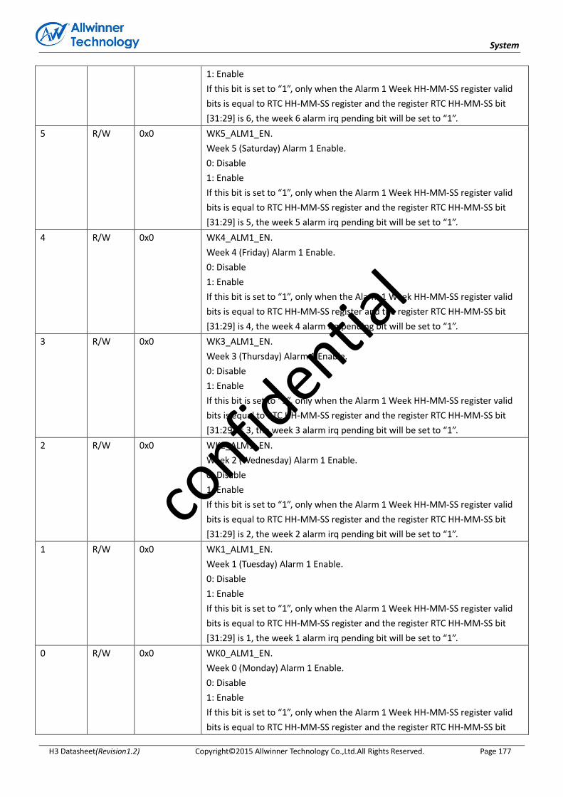
System
H3 Datasheet(Revision1.2) Copyright© 2015 Allwinner Technology Co.,Ltd.All Rights Reserved. Page 177
1: Enable
If this bit is set to “1”, only when the Alarm 1 Week HH-MM-SS register valid
bits is equal to RTC HH-MM-SS register and the register RTC HH-MM-SS bit
[31:29] is 6, the week 6 alarm irq pending bit will be set to “1”.
5 R/W 0x0 WK5_ALM1_EN.
Week 5 (Saturday) Alarm 1 Enable.
0: Disable
1: Enable
If this bit is set to “1”, only when the Alarm 1 Week HH-MM-SS register valid
bits is equal to RTC HH-MM-SS register and the register RTC HH-MM-SS bit
[31:29] is 5, the week 5 alarm irq pending bit will be set to “1”.
4 R/W 0x0 WK4_ALM1_EN.
Week 4 (Friday) Alarm 1 Enable.
0: Disable
1: Enable
If this bit is set to “1”, only when the Alarm 1 Week HH-MM-SS register valid
bits is equal to RTC HH-MM-SS register and the register RTC HH-MM-SS bit
[31:29] is 4, the week 4 alarm irq pending bit will be set to “1”.
3 R/W 0x0 WK3_ALM1_EN.
Week 3 (Thursday) Alarm 1 Enable.
0: Disable
1: Enable
If this bit is set to “1”, only when the Alarm 1 Week HH-MM-SS register valid
bits is equal to RTC HH-MM-SS register and the register RTC HH-MM-SS bit
[31:29] is 3, the week 3 alarm irq pending bit will be set to “1”.
2 R/W 0x0 WK2_ALM1_EN.
Week 2 (Wednesday) Alarm 1 Enable.
0: Disable
1: Enable
If this bit is set to “1”, only when the Alarm 1 Week HH-MM-SS register valid
bits is equal to RTC HH-MM-SS register and the register RTC HH-MM-SS bit
[31:29] is 2, the week 2 alarm irq pending bit will be set to “1”.
1 R/W 0x0 WK1_ALM1_EN.
Week 1 (Tuesday) Alarm 1 Enable.
0: Disable
1: Enable
If this bit is set to “1”, only when the Alarm 1 Week HH-MM-SS register valid
bits is equal to RTC HH-MM-SS register and the register RTC HH-MM-SS bit
[31:29] is 1, the week 1 alarm irq pending bit will be set to “1”.
0 R/W 0x0 WK0_ALM1_EN.
Week 0 (Monday) Alarm 1 Enable.
0: Disable
1: Enable
If this bit is set to “1”, only when the Alarm 1 Week HH-MM-SS register valid
bits is equal to RTC HH-MM-SS register and the register RTC HH-MM-SS bit
confid
ential
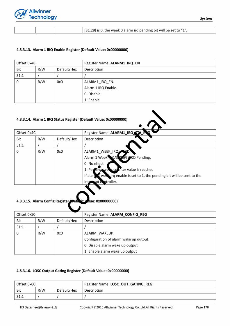
System
H3 Datasheet(Revision1.2) Copyright© 2015 Allwinner Technology Co.,Ltd.All Rights Reserved. Page 178
[31:29] is 0, the week 0 alarm irq pending bit will be set to “1”.
4.8.3.13. Alarm 1 IRQ Enable Register (Default Value: 0x00000000)
Offset:0x48 Register Name: ALARM1_IRQ_EN
Bit R/W Default/Hex Description
31:1 / / /
0 R/W 0x0 ALARM1_IRQ_EN.
Alarm 1 IRQ Enable.
0: Disable
1: Enable
4.8.3.14. Alarm 1 IRQ Status Register (Default Value: 0x00000000)
Offset:0x4C Register Name: ALARM1_IRQ_STA_REG
Bit R/W Default/Hex Description
31:1 / / /
0 R/W 0x0 ALARM1_WEEK_IRQ_PEND.
Alarm 1 Week (0/1/2/3/4/5/6) IRQ Pending.
0: No effect
1: Pending, week counter value is reached
If alarm 1 week irq enable is set to 1, the pending bit will be sent to the
interrupt controller.
4.8.3.15. Alarm Config Register (Default Value: 0x00000000)
Offset:0x50 Register Name: ALARM_CONFIG_REG
Bit R/W Default/Hex Description
31:1 / / /
0 R/W 0x0 ALARM_WAKEUP.
Configuration of alarm wake up output.
0: Disable alarm wake up output
1: Enable alarm wake up output
4.8.3.16. LOSC Output Gating Register (Default Value: 0x00000000)
Offset:0x60 Register Name: LOSC_OUT_GATING_REG
Bit R/W Default/Hex Description
31:1 / / /
confid
ential

System
H3 Datasheet(Revision1.2) Copyright© 2015 Allwinner Technology Co.,Ltd.All Rights Reserved. Page 179
0 R/W 0x0 LOSC_OUT_GATING.
Configuration of LOSC output, and no LOSC output by default.
0: Enable LOSC output gating
1: Disable LOSC output gating
4.8.3.17. General Purpose Register (Default Value: 0x00000000))
Offset:0x100+N *0x4
(N=0~7)
Register Name: GP_DATA_REGn
Bit R/W Default/Hex Description
31:0 R/W 0x0 GP_DATA.
Data [31:0].
Note: general purpose register 0~7 value can be stored if the VDD_RTC is larger than 1.0v.
4.8.3.18. RTC Debug Register (Default Value: 0x00000000)
Offset:0x170 Register Name: RTC_DEB_REG
Bit R/W Default/Hex Description
31:2 / / /
1 R/W 0x0 RTC_TEST_MODE_CTRL.
RTC TEST Mode Control bit.
0 R/W 0x0 RTC_DEBUG.
RTC Simulation Control bit
0: No effect. 1: simulation mode
4.8.3.19. GPL Hold Output Register (Default Value: 0x00000000)
Offset:0x180 Register Name: GPL_HOLD_OUTPUT_REG
Bit R/W Default/Hex Description
31:12 / / /
11 R/W 0x0 GPL11_HOLD_OUTPUT.
Hold the output of GPIOL11 when system’s power is changing. The output
must be low level (0) or high level (1) or High-Z; any other outputs may not
hold on.
0: Hold disable
1: Hold enable
10 R/W 0x0 GPL10_HOLD_OUTPUT.
Hold the output of GPIOL10 when system’s power is changing. The output
must be low level (0) or high level (1) or High-Z; any other outputs may not
hold on.
confid
ential

System
H3 Datasheet(Revision1.2) Copyright© 2015 Allwinner Technology Co.,Ltd.All Rights Reserved. Page 180
0: Hold disable
1: Hold enable
9 R/W 0x0 GPL9_HOLD_OUTPUT.
Hold the output of GPIOL9 when system’s power is changing. The output
must be low level (0) or high level (1) or High-Z; any other outputs may not
hold on.
0: Hold disable
1: Hold enable
8 R/W 0x0 GPL8_HOLD_OUTPUT.
Hold the output of GPIOL8 when system’s power is changing. The output
must be low level (0) or high level (1) or High-Z; any other outputs may not
hold on.
0: Hold disable
1: Hold enable
7 R/W 0x0 GPL7_HOLD_OUTPUT.
Hold the output of GPIOL7 when system’s power is changing. The output
must be low level (0) or high level (1) or High-Z; any other outputs may not
hold on.
0: Hold disable
1: Hold enable
6 R/W 0x0 GPL6_HOLD_OUTPUT.
Hold the output of GPIOL6 when system’s power is changing. The output
must be low level (0) or high level (1) or High-Z; any other outputs may not
hold on.
0: Hold disable
1: Hold enable
5 R/W 0x0 GPL5_HOLD_OUTPUT.
Hold the output of GPIOL5 when system’s power is changing. The output
must be low level (0) or high level (1) or High-Z; any other outputs may not
hold on.
0: Hold disable
1: Hold enable
4 R/W 0x0 GPL4_HOLD_OUTPUT.
Hold the output of GPIOL4 when system’s power is changing. The outputs
must be low level (0) or high level (1) or High-Z; any other output may not
hold on.
0: Hold disable
1: Hold enable
3 R/W 0x0 GPL3_HOLD_OUTPUT.
Hold the output of GPIOL3 when system’s power is changing. The output
must be low level (0) or high level (1) or High-Z; any other outputs may not
hold on.
0: Hold disable
1: Hold enable
2 R/W 0x0 GPL2_HOLD_OUTPUT.
confid
ential

System
H3 Datasheet(Revision1.2) Copyright© 2015 Allwinner Technology Co.,Ltd.All Rights Reserved. Page 181
Hold the output of GPIOL2 when system’s power is changing. The output
must be low level (0) or high level (1) or High-Z; any other outputs may not
hold on.
0: Hold disable
1: Hold enable
1 R/W 0x0 GPL1_HOLD_OUTPUT.
Hold the output of GPIOL1 when system’s power is changing. The output
must be low level (0) or high level (1) or High-Z; any other outputs may not
hold on.
0: Hold disable
1: Hold enable
0 R/W 0x0 GPL0_HOLD_OUTPUT.
Hold the output of GPIOL0 when system’s power is changing. The output
must be low level (0) or high level (1) or High-Z; any other outputs may not
hold on.
0: Hold disable
1: Hold enable
4.8.3.20. VDD RTC Regulation Register (Default Value: 0x00000004)
Offset:0x190 Register Name: VDD_RTC_REG
Bit R/W Default/Hex Description
31:3 / / /
2:0 R/W 0x100 VDD_RTC_REGU.
These bits are useful for regulating the RTC_VIO from 0.7v to 1.4v, and the
regulation step is 0.1v.
000: 0.7v
001: 0.8v
010: 0.9v
011: 1.0v
100: 1.1v
101: 1.2v
110: 1.3v
111: 1.4v
4.8.3.21. IC Characteristic Register (Default Value: 0x00000000)
Offset:0x1F0 Register Name: IC_CHARA_REG
Bit Read/Write Default/Hex Description
31:16 R/W 0x0 IC_CHARA.
Key Field.
Should be written at value 0x16AA. Writing any other value in this field
confid
ential

System
H3 Datasheet(Revision1.2) Copyright© 2015 Allwinner Technology Co.,Ltd.All Rights Reserved. Page 182
aborts the write operation.
15:0 R/W 0x0 ID_DATA.
Return 0x16aa only if the KEY_FIELD is set as 0x16aa when read those bits,
otherwise return 0x0.
confid
ential
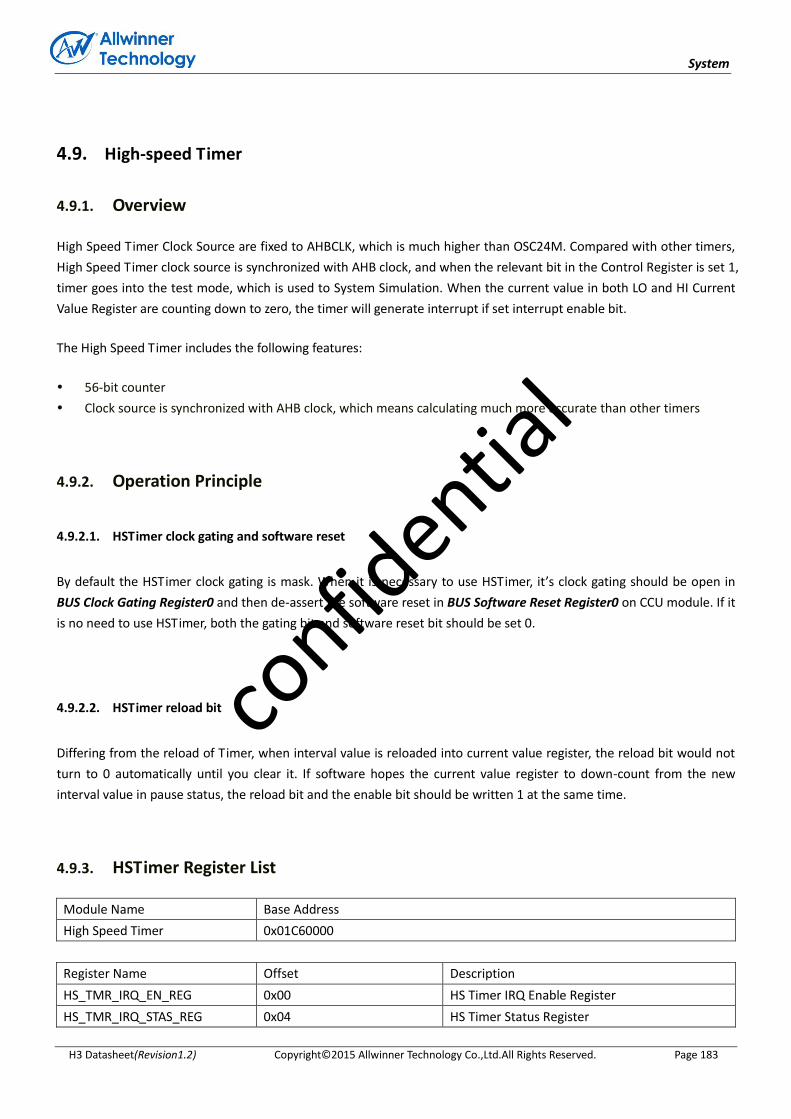
System
H3 Datasheet(Revision1.2) Copyright© 2015 Allwinner Technology Co.,Ltd.All Rights Reserved. Page 183
4.9. High-speed Timer
4.9.1. Overview
High Speed Timer Clock Source are fixed to AHBCLK, which is much higher than OSC24M. Compared with other timers,
High Speed Timer clock source is synchronized with AHB clock, and when the relevant bit in the Control Register is set 1,
timer goes into the test mode, which is used to System Simulation. When the current value in both LO and HI Current
Value Register are counting down to zero, the timer will generate interrupt if set interrupt enable bit.
The High Speed Timer includes the following features:
56-bit counter
Clock source is synchronized with AHB clock, which means calculating much more accurate than other timers
4.9.2. Operation Principle
4.9.2.1. HSTimer clock gating and software reset
By default the HSTimer clock gating is mask. When it is necessary to use HSTimer, it’s clock gating should be open in
BUS Clock Gating Register0 and then de-assert the software reset in BUS Software Reset Register0 on CCU module. If it
is no need to use HSTimer, both the gating bit and software reset bit should be set 0.
4.9.2.2. HSTimer reload bit
Differing from the reload of Timer, when interval value is reloaded into current value register, the reload bit would not
turn to 0 automatically until you clear it. If software hopes the current value register to down-count from the new
interval value in pause status, the reload bit and the enable bit should be written 1 at the same time.
4.9.3. HSTimer Register List
Module Name Base Address
High Speed Timer 0x01C60000
Register Name Offset Description
HS_TMR_IRQ_EN_REG 0x00 HS Timer IRQ Enable Register
HS_TMR_IRQ_STAS_REG 0x04 HS Timer Status Register
confid
ential
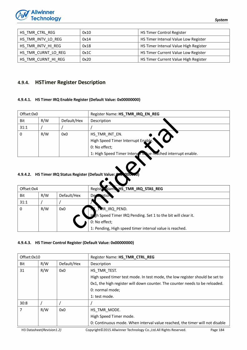
System
H3 Datasheet(Revision1.2) Copyright© 2015 Allwinner Technology Co.,Ltd.All Rights Reserved. Page 184
HS_TMR_CTRL_REG 0x10 HS Timer Control Register
HS_TMR_INTV_LO_REG 0x14 HS Timer Interval Value Low Register
HS_TMR_INTV_HI_REG 0x18 HS Timer Interval Value High Register
HS_TMR_CURNT_LO_REG 0x1C HS Timer Current Value Low Register
HS_TMR_CURNT_HI_REG 0x20 HS Timer Current Value High Register
4.9.4. HSTimer Register Description
4.9.4.1. HS Timer IRQ Enable Register (Default Value: 0x00000000)
Offset:0x0 Register Name: HS_TMR_IRQ_EN_REG
Bit R/W Default/Hex Description
31:1 / / /
0 R/W 0x0 HS_TMR_INT_EN.
High Speed Timer Interrupt Enable.
0: No effect;
1: High Speed Timer Interval Value reached interrupt enable.
4.9.4.2. HS Timer IRQ Status Register (Default Value: 0x00000000)
Offset:0x4 Register Name: HS_TMR_IRQ_STAS_REG
Bit R/W Default/Hex Description
31:1 / / /
0 R/W 0x0 HS_TMR_IRQ_PEND.
High Speed Timer IRQ Pending. Set 1 to the bit will clear it.
0: No effect;
1: Pending, High speed timer interval value is reached.
4.9.4.3. HS Timer Control Register (Default Value: 0x00000000)
Offset:0x10 Register Name: HS_TMR_CTRL_REG
Bit R/W Default/Hex Description
31 R/W 0x0 HS_TMR_TEST.
High speed timer test mode. In test mode, the low register should be set to
0x1, the high register will down counter. The counter needs to be reloaded.
0: normal mode;
1: test mode.
30:8 / / /
7 R/W 0x0 HS_TMR_MODE.
High Speed Timer mode.
0: Continuous mode. When interval value reached, the timer will not disable
confid
ential

System
H3 Datasheet(Revision1.2) Copyright© 2015 Allwinner Technology Co.,Ltd.All Rights Reserved. Page 185
automatically.
1: Single mode. When interval value reached, the timer will disable
automatically.
6:4 R/W 0x0 HS_TMR_CLK
Select the pre-scale of the high speed timer clock sources.
000: /1
001: /2
010: /4
011: /8
100: /16
101: /
110: /
111: /
3:2 / / /
1 R/W 0x0 HS_TMR_RELOAD.
High Speed Timer Reload.
0: No effect, 1: Reload High Speed Timer Interval Value.
0 R/W 0x0 HS_TMR_EN.
High Speed Timer Enable.
0: Stop/Pause, 1: Start.
If the timer is started, it will reload the interval value to internal register, and
the current counter will count from interval value to 0.
If the current counter does not reach the zero, the timer enable bit is set to
“0”, the current value counter will pause. At least wait for 2 cycles, the start
bit can be set to 1.
In timer pause state, the interval value register can be modified. If the timer
is started again, and the Software hope the current value register to
down-count from the new interval value, the reload bit and the enable bit
should be set to 1 at the same time.
4.9.4.4. HS Timer Interval Value Lo Register
Offset:0x14 Register Name: HS_TMR_INTV_LO_REG
Bit R/W Default/Hex Description
31:0 R/W x HS_TMR_INTV_VALUE_LO.
High Speed Timer Interval Value [31:0].
4.9.4.5. HS Timer Interval Value Hi Register
Offset:0x18 Register Name: HS_TMR_INTV_HI_REG
Bit R/W Default/Hex Description
31:24 / / /
23:0 R/W x HS_TMR_INTV_VALUE_HI.
confid
ential

System
H3 Datasheet(Revision1.2) Copyright© 2015 Allwinner Technology Co.,Ltd.All Rights Reserved. Page 186
High Speed Timer Interval Value [55:32].
Note:The interval value register is a 56-bit register. When read or write the interval value, the Lo register should be read
or write first. And the Hi register should be written after the Lo register.
4.9.4.6. HS Timer Current Value Lo Register
Offset:0x1C Register Name: HS_TMR_CURNT_LO_REG
Bit R/W Default/Hex Description
31:0 R/W x HS_TMR_CUR_VALUE_LO.
High Speed Timer Current Value [31:0].
4.9.4.7. HS Timer Current Value Hi Register
Offset:0x20 Register Name: HS_TMR_CURNT_HI_REG
Bit R/W Default/Hex Description
31:24 / / /
23:0 R/W x HS_TMR_CUR_VALUE_HI.
High Speed Timer Current Value [55:32].
Note1:HSTimer current value is a 56-bit down-counter (from interval value to 0).
Note2:The current value register is a 56-bit register. When read or write the current value, the Lo register should be
read or write first.
4.9.5. Programming Guidelines
Take making a 1us delay using HSTimer for an instance as follow, AHB1CLK will be configurated as 100MHz and n_mode,
Single mode and 2 pre-scale will be selected in this instance.
writel(0x0, HS_TMR_INTV_HI); //Set interval value Hi 0x0
writel(0x32, HS_TMR_INTV_LO); //Set interval value Lo 0x32
writel(0x90, HS_TMR_CTRL); //Select n_mode,2 pre-scale,single mode
writel(readl(HS_TMR_CTRL)|(1<<1), HS_TMR_CTRL); //Set Reload bit
writel(readl(HS_TMR_CTRL)|(1<<0), HS_TMR_CTRL); //Enable HSTimer
While(!(readl(HS_TMR_IRQ_STAT)&1)); //Wait for HSTimer to generate pending
Writel(1,HS_TMR_IRQ_STAT); //Clear HSTimer pending
confid
ential

System
H3 Datasheet(Revision1.2) Copyright© 2015 Allwinner Technology Co.,Ltd.All Rights Reserved. Page 187
4.10. PWM
4.10.1. Overview
The output of the PWM is a toggling signal whose frequency and duty cycle can be modulated by its programmable
registers. Each channel has a dedicated internal 16-bit up counter. If the counter reaches the value stored in the channel
period register, it resets. At the beginning of a count period cycle, the PWMOUT is set to active state and count from
0x0000.The PWM divider divides the clock(24MHz) by 1~4096 according to the pre-scalar bits in the PWM control
register.
In PWM cycle mode, the output will be a square waveform, the frequency is set to the period register. In PWM pulse
mode, the output will be a positive pulse or a negative pulse.
4.10.2. PWM Block Diagram
Cycle Mode
Entire cycles
Active lowActive cycles
Pulse Mode
Active highActive cycles
Figure 4-5. PWM Block Diagram
When PWM is enabling, the PWM can output two signals, which are reversed on two pins. And when PWM is disabling,
the PWM can control the status of two pins. The PWM divider divides the clock (24MHz) by 1-64 according to the
pre-scalar bits in the PWM control register. The PWM output Frequency can be divided by 65536 at most. In PWM cycle
mode, the output will be a square waveform; the frequency is set to the period register. In PWM pulse mode, the
output will be a positive pulse or a negative pulse.
4.10.3. PWM Register List
Module Name Base Address
PWM 0x01C21400
Register Name Offset Description
PWM_CH_CTRL 0x00 PWM Control Register
PWM_CH0_PERIOD 0x04 PWM Channel 0 Period Register
confid
ential
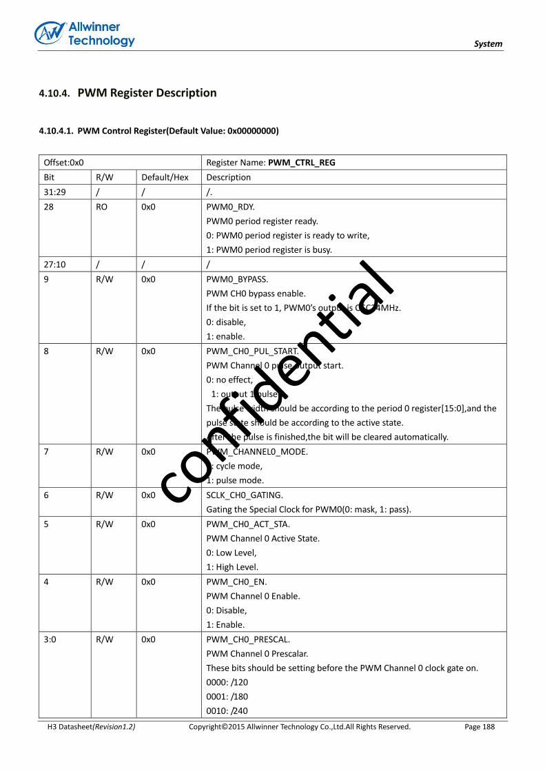
System
H3 Datasheet(Revision1.2) Copyright© 2015 Allwinner Technology Co.,Ltd.All Rights Reserved. Page 188
4.10.4. PWM Register Description
4.10.4.1. PWM Control Register(Default Value: 0x00000000)
Offset:0x0 Register Name: PWM_CTRL_REG
Bit R/W Default/Hex Description
31:29 / / /.
28 RO 0x0 PWM0_RDY.
PWM0 period register ready.
0: PWM0 period register is ready to write,
1: PWM0 period register is busy.
27:10 / / /
9 R/W 0x0 PWM0_BYPASS.
PWM CH0 bypass enable.
If the bit is set to 1, PWM0’s output is OSC24MHz.
0: disable,
1: enable.
8 R/W 0x0 PWM_CH0_PUL_START.
PWM Channel 0 pulse output start.
0: no effect,
1: output 1 pulse.
The pulse width should be according to the period 0 register[15:0],and the
pulse state should be according to the active state.
After the pulse is finished,the bit will be cleared automatically.
7 R/W 0x0 PWM_CHANNEL0_MODE.
0: cycle mode,
1: pulse mode.
6 R/W 0x0 SCLK_CH0_GATING.
Gating the Special Clock for PWM0(0: mask, 1: pass).
5 R/W 0x0 PWM_CH0_ACT_STA.
PWM Channel 0 Active State.
0: Low Level,
1: High Level.
4 R/W 0x0 PWM_CH0_EN.
PWM Channel 0 Enable.
0: Disable,
1: Enable.
3:0 R/W 0x0 PWM_CH0_PRESCAL.
PWM Channel 0 Prescalar.
These bits should be setting before the PWM Channel 0 clock gate on.
0000: /120
0001: /180
0010: /240
confid
ential

System
H3 Datasheet(Revision1.2) Copyright© 2015 Allwinner Technology Co.,Ltd.All Rights Reserved. Page 189
0011: /360
0100: /480
0101: /
0110: /
0111: /
1000: /12k
1001: /24k
1010: /36k
1011: /48k
1100: /72k
1101: /
1110: /
1111: /1
4.10.4.2. PWM Channel 0 Period Register(Default Value: 0x00000000)
Offset:0x4 Register Name: PWM_CH0_PERIOD
Bit R/W Default/Hex Description
31:16 R/W x PWM_CH0_ENTIRE_CYS
Number of the entire cycles in the PWM clock.
0 = 1 cycle
1 = 2 cycles
……
N = N+1 cycles
If the register need to be modified dynamically, the PCLK should be faster
than the PWM CLK (PWM CLK = 24MHz/pre-scale).
15:0 R/W x PWM_CH0_ENTIRE_ACT_CYS
Number of the active cycles in the PWM clock.
0 = 0 cycle
1 = 1 cycles
……
N = N cycles
Note:The active cycles should be no larger than the period cycles.
confid
ential

System
H3 Datasheet(Revision1.2) Copyright© 2015 Allwinner Technology Co.,Ltd.All Rights Reserved. Page 190
4.11. DMA
4.11.1. Overview
There are 12 DMA channels in the chip. Each DMA channel can generate interrupts. According to different pending
status, the referenced DMA channel generates corresponding interrupt. And, the configuration information of every
DMA channel are storing in the DDR or SRAM. When start a DMA transferring, the DMA Channel Descriptor Address
Register contains the address information in the DDR or SRAM, where has the relevance configuration information of
the DMA transferring.
4.11.2. Functionalities Description
4.11.2.1. Block Diagram
Source
Address
Configuration
Destination
Address
Byte Counter
Link
Descriptor information Pending Status
Pkg
-pen
d
End-p
end
Commity
Parameter
Hal
f-pen
d
Request DMA
Any
Idle?
Write Descriptor
Address and Start DMA
Transferring Package
Pause?
Link=fffff 800?
DMA Transfer Progress
Prepare Descriptor Data
1Link
2Link
3Link
40xfffff 800
Pkg
-pen
d
Hal
f-pen
d
Pkg
-pen
d
Hal
f-pen
d
Pkf-
pen
d
Hal
f-pen
d
After transferring a half data of a pkg, the pkg half pending bit would set up
After transferring all data of pkg, the pkg end pending bit would set up
After finishing a transmission, the queue end pending bit would set up
Link is used to storing next descriptor address or transmission end flag (0xfffff800)
Pkg-pend
Half-pend
Yes
Resume
No
No
End-pend
Transmission Finish
DMA
DMAC obtains
Descriptor information
Figure 4-6. DMA Block Diagram
confid
ential

System
H3 Datasheet(Revision1.2) Copyright© 2015 Allwinner Technology Co.,Ltd.All Rights Reserved. Page 191
4.11.2.2. DRQ Type and Corresponding Relation
Table 4-1. DMA DRQ Table
Source DRQ Type Destination DRQ Type
Port NO. Module Name Port NO. Module Name
Port 0 SRAM Port 0 SRAM
Port 1 SDRAM Port 1 SDRAM
Port 2 / Port 2 OWA_TX
Port 3 I2S/PCM 0_RX Port 3 I2S/PCM 0_TX
Port 4 I2S/PCM 1_RX Port 4 I2S/PCM 1_TX
Port 5 NAND Port 5 NAND
Port 6 UART0_RX Port 6 UART0_TX
Port 7 UART1_RX Port 7 UART1_TX
Port 8 UART2_RX Port 8 UART2_TX
Port 9 UART3_RX Port 9 UART3_TX
Port 10 / Port 10 /
Port 11 / Port 11 /
Port 12 / Port 12 /
Port 13 / Port 13 /
Port 14 / Port 14 /
Port 15 Audio Codec Port 15 Audio Codec
Port 16 / Port 16 /
Port 17 USB OTG_Device_EP1 Port 17 USB OTG_Device_EP1
Port 18 USB OTG_Device_EP2 Port 18 USB OTG_Device_EP2
Port 19 USB OTG_Device_EP3 Port 19 USB OTG_Device_EP3
Port20 USB OTG_Device_EP4 Port 20 USB OTG_Device_EP4
Port 21 / Port 21 /
Port 22 / Port 22 /
Port 23 SPI0_RX Port 23 SPI0_TX
Port 24 SPI1_RX Port 24 SPI1_TX
Port 25 Port 25
Port 26 Port 26
Port 27 Port 27 I2S/PCM 2_TX
Port 28 Port 28
Port 29 Port 29
Port 30 Port 30
Note:SRAM or DRAM DRQ signal is always high.
4.11.2.3. DMA Descriptor
In this section, the DMA descriptor registers will be introduced in detail.
When starting a DMA transmission, the module data are transferred as packages, which have the link data information.
confid
ential
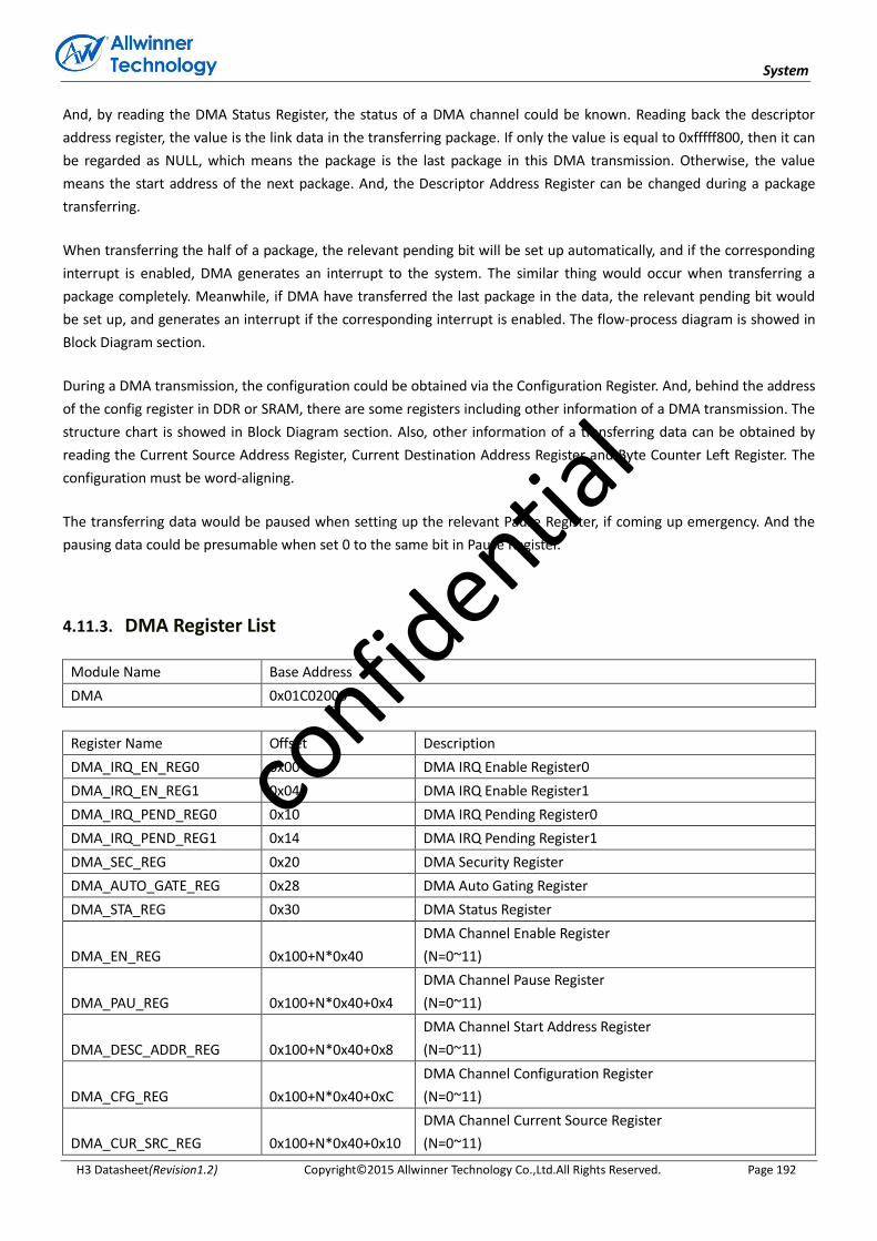
System
H3 Datasheet(Revision1.2) Copyright© 2015 Allwinner Technology Co.,Ltd.All Rights Reserved. Page 192
And, by reading the DMA Status Register, the status of a DMA channel could be known. Reading back the descriptor
address register, the value is the link data in the transferring package. If only the value is equal to 0xfffff800, then it can
be regarded as NULL, which means the package is the last package in this DMA transmission. Otherwise, the value
means the start address of the next package. And, the Descriptor Address Register can be changed during a package
transferring.
When transferring the half of a package, the relevant pending bit will be set up automatically, and if the corresponding
interrupt is enabled, DMA generates an interrupt to the system. The similar thing would occur when transferring a
package completely. Meanwhile, if DMA have transferred the last package in the data, the relevant pending bit would
be set up, and generates an interrupt if the corresponding interrupt is enabled. The flow-process diagram is showed in
Block Diagram section.
During a DMA transmission, the configuration could be obtained via the Configuration Register. And, behind the address
of the config register in DDR or SRAM, there are some registers including other information of a DMA transmission. The
structure chart is showed in Block Diagram section. Also, other information of a transferring data can be obtained by
reading the Current Source Address Register, Current Destination Address Register and Byte Counter Left Register. The
configuration must be word-aligning.
The transferring data would be paused when setting up the relevant Pause Register, if coming up emergency. And the
pausing data could be presumable when set 0 to the same bit in Pause Register.
4.11.3. DMA Register List
Module Name Base Address
DMA 0x01C02000
Register Name Offset Description
DMA_IRQ_EN_REG0 0x00 DMA IRQ Enable Register0
DMA_IRQ_EN_REG1 0x04 DMA IRQ Enable Register1
DMA_IRQ_PEND_REG0 0x10 DMA IRQ Pending Register0
DMA_IRQ_PEND_REG1 0x14 DMA IRQ Pending Register1
DMA_SEC_REG 0x20 DMA Security Register
DMA_AUTO_GATE_REG 0x28 DMA Auto Gating Register
DMA_STA_REG 0x30 DMA Status Register
DMA_EN_REG 0x100+N*0x40
DMA Channel Enable Register
(N=0~11)
DMA_PAU_REG 0x100+N*0x40+0x4
DMA Channel Pause Register
(N=0~11)
DMA_DESC_ADDR_REG 0x100+N*0x40+0x8
DMA Channel Start Address Register
(N=0~11)
DMA_CFG_REG 0x100+N*0x40+0xC
DMA Channel Configuration Register
(N=0~11)
DMA_CUR_SRC_REG 0x100+N*0x40+0x10
DMA Channel Current Source Register
(N=0~11)
confid
ential

System
H3 Datasheet(Revision1.2) Copyright© 2015 Allwinner Technology Co.,Ltd.All Rights Reserved. Page 193
DMA_CUR_DEST_REG 0x100+N*0x40+0x14
DMA Channel Current Destination Register
(N=0~11)
DMA_BCNT_LEFT_REG 0x100+N*0x40+0x18
DMA Channel Byte Counter Left Register
(N=0~11)
DMA_PARA_REG 0x100+N*0x40+0x1C
DMA Channel Parameter Register
(N=0~11)
DMA_FDESC_ADDR_REG 0x100+N*0x40+0x2C
DMA Formar Descriptor Address Register
(N=0~11)
DMA_PKG_NUM_REG 0x100+N*0x40+0x30
DMA Package Number Register
(N=0~11)
4.11.4. DMA Register Description
4.11.4.1. DMA IRQ Enable Register0 (Default Value: 0x00000000)
Offset: 0x0000 Register Name: DMA_IRQ_EN_REG0
Bit R/W Default/Hex Description
31 / / /
30 R/W 0x0 DMA7_QUEUE_IRQ_EN
DMA 7 Queue End Transfer Interrupt Enable.
0: Disable, 1: Enable.
29 R/W 0x0 DMA7_PKG_IRQ_EN
DMA 7 Package End Transfer Interrupt Enable.
0: Disable, 1: Enable.
28 R/W 0x0 DMA7_HLAF_IRQ_EN
DMA 7 Half Package Transfer Interrupt Enable.
0: Disable, 1: Enable.
27 / / /
26 R/W 0x0 DMA6_QUEUE_IRQ_EN
DMA 6 Queue End Transfer Interrupt Enable.
0: Disable, 1: Enable.
25 R/W 0x0 DMA6_PKG_IRQ_EN
DMA 6 Package End Transfer Interrupt Enable.
0: Disable, 1: Enable.
24 R/W 0x0 DMA6_HLAF_IRQ_EN
DMA 6 Half Package Transfer Interrupt Enable.
0: Disable, 1: Enable.
23 / / /
22 R/W 0x0 DMA5_QUEUE_IRQ_EN
DMA 5 Queue End Transfer Interrupt Enable.
0: Disable, 1: Enable.
21 R/W 0x0 DMA5_PKG_IRQ_EN
confid
ential
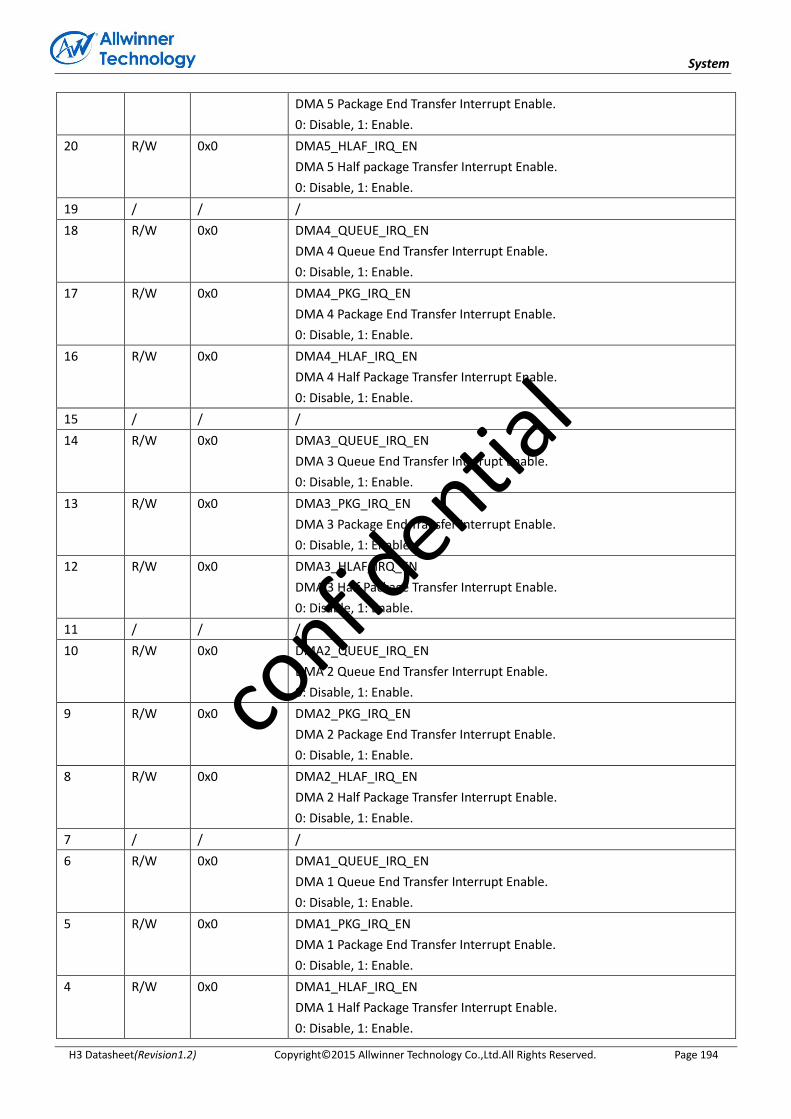
System
H3 Datasheet(Revision1.2) Copyright© 2015 Allwinner Technology Co.,Ltd.All Rights Reserved. Page 194
DMA 5 Package End Transfer Interrupt Enable.
0: Disable, 1: Enable.
20 R/W 0x0 DMA5_HLAF_IRQ_EN
DMA 5 Half package Transfer Interrupt Enable.
0: Disable, 1: Enable.
19 / / /
18 R/W 0x0 DMA4_QUEUE_IRQ_EN
DMA 4 Queue End Transfer Interrupt Enable.
0: Disable, 1: Enable.
17 R/W 0x0 DMA4_PKG_IRQ_EN
DMA 4 Package End Transfer Interrupt Enable.
0: Disable, 1: Enable.
16 R/W 0x0 DMA4_HLAF_IRQ_EN
DMA 4 Half Package Transfer Interrupt Enable.
0: Disable, 1: Enable.
15 / / /
14 R/W 0x0 DMA3_QUEUE_IRQ_EN
DMA 3 Queue End Transfer Interrupt Enable.
0: Disable, 1: Enable.
13 R/W 0x0 DMA3_PKG_IRQ_EN
DMA 3 Package End Transfer Interrupt Enable.
0: Disable, 1: Enable.
12 R/W 0x0 DMA3_HLAF_IRQ_EN
DMA 3 Half Package Transfer Interrupt Enable.
0: Disable, 1: Enable.
11 / / /
10 R/W 0x0 DMA2_QUEUE_IRQ_EN
DMA 2 Queue End Transfer Interrupt Enable.
0: Disable, 1: Enable.
9 R/W 0x0 DMA2_PKG_IRQ_EN
DMA 2 Package End Transfer Interrupt Enable.
0: Disable, 1: Enable.
8 R/W 0x0 DMA2_HLAF_IRQ_EN
DMA 2 Half Package Transfer Interrupt Enable.
0: Disable, 1: Enable.
7 / / /
6 R/W 0x0 DMA1_QUEUE_IRQ_EN
DMA 1 Queue End Transfer Interrupt Enable.
0: Disable, 1: Enable.
5 R/W 0x0 DMA1_PKG_IRQ_EN
DMA 1 Package End Transfer Interrupt Enable.
0: Disable, 1: Enable.
4 R/W 0x0 DMA1_HLAF_IRQ_EN
DMA 1 Half Package Transfer Interrupt Enable.
0: Disable, 1: Enable.
confid
ential

System
H3 Datasheet(Revision1.2) Copyright© 2015 Allwinner Technology Co.,Ltd.All Rights Reserved. Page 195
3 / / /
2 R/W 0x0 DMA0_QUEUE_IRQ_EN
DMA 0 Queue End Transfer Interrupt Enable.
0: Disable, 1: Enable.
1 R/W 0x0 DMA0_PKG_IRQ_EN
DMA 0 Package End Transfer Interrupt Enable.
0: Disable, 1: Enable.
0 R/W 0x0 DMA0_HLAF_IRQ_EN
DMA 0 Half Package Transfer Interrupt Enable.
0: Disable, 1: Enable
4.11.4.2. DMA IRQ Enable Register1 (Default Value: 0x00000000)
Offset: 0x0004 Register Name: DMA_IRQ_EN_REG1
Bit R/W Default/Hex Description
31:15 / / /
14 R/W 0x0 DMA11_QUEUE_IRQ_EN
DMA 11 Queue End Transfer Interrupt Enable.
0: Disable, 1: Enable.
13 R/W 0x0 DMA11_PKG_IRQ_EN
DMA 11 Package End Transfer Interrupt Enable.
0: Disable
1: Enable
12 R/W 0x0 DMA11_HLAF_IRQ_EN
DMA 11 Half Package Transfer Interrupt Enable.
0: Disable
1: Enable
11 / / /
10 R/W 0x0 DMA10_QUEUE_IRQ_EN
DMA 10 Queue End Transfer Interrupt Enable.
0: Disable
1: Enable
9 R/W 0x0 DMA10_PKG_IRQ_EN
DMA 10 Package End Transfer Interrupt Enable.
0: Disable
1: Enable
8 R/W 0x0 DMA10_HLAF_IRQ_EN
DMA 10 Half Package Transfer Interrupt Enable.
0: Disable
1: Enable
7 / / /
6 R/W 0x0 DMA9_QUEUE_IRQ_EN
DMA 9 Queue End Transfer Interrupt Enable.
0: Disable
confid
ential

System
H3 Datasheet(Revision1.2) Copyright© 2015 Allwinner Technology Co.,Ltd.All Rights Reserved. Page 196
1: Enable
5 R/W 0x0 DMA9_PKG_IRQ_EN
DMA 9 Package End Transfer Interrupt Enable.
0: Disable
1: Enable
4 R/W 0x0 DMA9_HLAF_IRQ_EN
DMA 9 Half package Transfer Interrupt Enable.
0: Disable
1: Enable
3 / / /
2 R/W 0x0 DMA8_QUEUE_IRQ_EN
DMA 8 Queue End Transfer Interrupt Enable.
0: Disable
1: Enable
1 R/W 0x0 DMA8_PKG_IRQ_EN
DMA 8 Package End Transfer Interrupt Enable.
0: Disable
1: Enable
0 R/W 0x0 DMA8_HLAF_IRQ_EN
DMA 8 Half Package Transfer Interrupt Enable.
0: Disable
1: Enable
4.11.4.3. DMA IRQ Pending Status Register0 (Default Value: 0x00000000)
Offset:0x10 Register Name: DMA_IRQ_PEND_REG0
Bit R/W Default/Hex Description
31 / / /
30 R/W 0x0 DMA7_QUEUE_IRQ_PEND.
DMA 7 Queue End Transfer Interrupt Pending. Set 1 to the bit will clear it.
0: No effect, 1: Pending.
29 R/W 0x0 DMA7_PKG_IRQ_ PEND
DMA 7 Package End Transfer Interrupt Pending. Set 1 to the bit will clear it.
0: No effect, 1: Pending.
28 R/W 0x0 DMA7_HLAF_IRQ_PEND.
DMA 7 Half Package Transfer Interrupt Pending. Set 1 to the bit will clear it.
0: No effect, 1: Pending.
27 / / /
26 R/W 0x0 DMA6_QUEUE_IRQ_PEND.
DMA 6 Queue End Transfer Interrupt Pending. Set 1 to the bit will clear it.
0: No effect, 1: Pending.
25 R/W 0x0 DMA6_PKG_IRQ_ PEND
DMA 6 Package End Transfer Interrupt Pending. Set 1 to the bit will clear it.
0: No effect, 1: Pending.
confid
ential
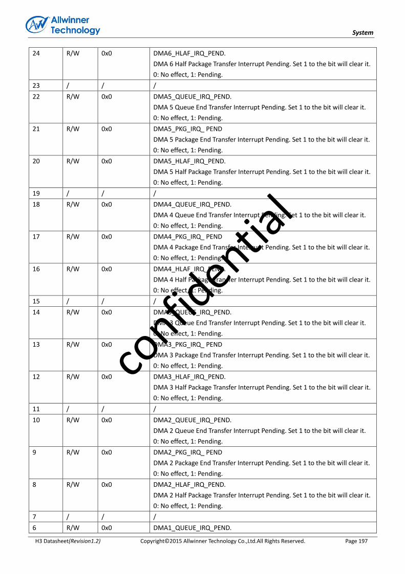
System
H3 Datasheet(Revision1.2) Copyright© 2015 Allwinner Technology Co.,Ltd.All Rights Reserved. Page 197
24 R/W 0x0 DMA6_HLAF_IRQ_PEND.
DMA 6 Half Package Transfer Interrupt Pending. Set 1 to the bit will clear it.
0: No effect, 1: Pending.
23 / / /
22 R/W 0x0 DMA5_QUEUE_IRQ_PEND.
DMA 5 Queue End Transfer Interrupt Pending. Set 1 to the bit will clear it.
0: No effect, 1: Pending.
21 R/W 0x0 DMA5_PKG_IRQ_ PEND
DMA 5 Package End Transfer Interrupt Pending. Set 1 to the bit will clear it.
0: No effect, 1: Pending.
20 R/W 0x0 DMA5_HLAF_IRQ_PEND.
DMA 5 Half Package Transfer Interrupt Pending. Set 1 to the bit will clear it.
0: No effect, 1: Pending.
19 / / /
18 R/W 0x0 DMA4_QUEUE_IRQ_PEND.
DMA 4 Queue End Transfer Interrupt Pending. Set 1 to the bit will clear it.
0: No effect, 1: Pending.
17 R/W 0x0 DMA4_PKG_IRQ_ PEND
DMA 4 Package End Transfer Interrupt Pending. Set 1 to the bit will clear it.
0: No effect, 1: Pending.
16 R/W 0x0 DMA4_HLAF_IRQ_PEND.
DMA 4 Half Package Transfer Interrupt Pending. Set 1 to the bit will clear it.
0: No effect, 1: Pending.
15 / / /
14 R/W 0x0 DMA3_QUEUE_IRQ_PEND.
DMA 3 Queue End Transfer Interrupt Pending. Set 1 to the bit will clear it.
0: No effect, 1: Pending.
13 R/W 0x0 DMA3_PKG_IRQ_ PEND
DMA 3 Package End Transfer Interrupt Pending. Set 1 to the bit will clear it.
0: No effect, 1: Pending.
12 R/W 0x0 DMA3_HLAF_IRQ_PEND.
DMA 3 Half Package Transfer Interrupt Pending. Set 1 to the bit will clear it.
0: No effect, 1: Pending.
11 / / /
10 R/W 0x0 DMA2_QUEUE_IRQ_PEND.
DMA 2 Queue End Transfer Interrupt Pending. Set 1 to the bit will clear it.
0: No effect, 1: Pending.
9 R/W 0x0 DMA2_PKG_IRQ_ PEND
DMA 2 Package End Transfer Interrupt Pending. Set 1 to the bit will clear it.
0: No effect, 1: Pending.
8 R/W 0x0 DMA2_HLAF_IRQ_PEND.
DMA 2 Half Package Transfer Interrupt Pending. Set 1 to the bit will clear it.
0: No effect, 1: Pending.
7 / / /
6 R/W 0x0 DMA1_QUEUE_IRQ_PEND.
confid
ential
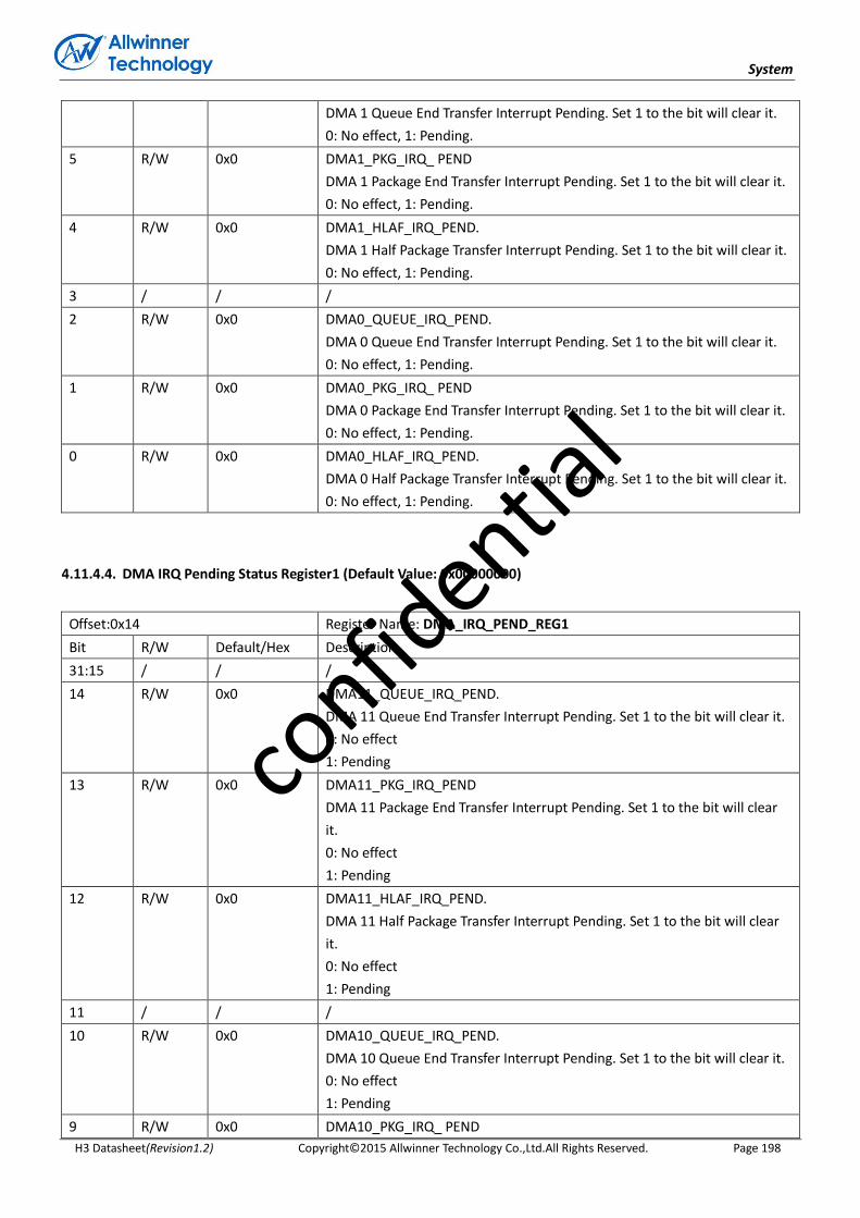
System
H3 Datasheet(Revision1.2) Copyright© 2015 Allwinner Technology Co.,Ltd.All Rights Reserved. Page 198
DMA 1 Queue End Transfer Interrupt Pending. Set 1 to the bit will clear it.
0: No effect, 1: Pending.
5 R/W 0x0 DMA1_PKG_IRQ_ PEND
DMA 1 Package End Transfer Interrupt Pending. Set 1 to the bit will clear it.
0: No effect, 1: Pending.
4 R/W 0x0 DMA1_HLAF_IRQ_PEND.
DMA 1 Half Package Transfer Interrupt Pending. Set 1 to the bit will clear it.
0: No effect, 1: Pending.
3 / / /
2 R/W 0x0 DMA0_QUEUE_IRQ_PEND.
DMA 0 Queue End Transfer Interrupt Pending. Set 1 to the bit will clear it.
0: No effect, 1: Pending.
1 R/W 0x0 DMA0_PKG_IRQ_ PEND
DMA 0 Package End Transfer Interrupt Pending. Set 1 to the bit will clear it.
0: No effect, 1: Pending.
0 R/W 0x0 DMA0_HLAF_IRQ_PEND.
DMA 0 Half Package Transfer Interrupt Pending. Set 1 to the bit will clear it.
0: No effect, 1: Pending.
4.11.4.4. DMA IRQ Pending Status Register1 (Default Value: 0x00000000)
Offset:0x14 Register Name: DMA_IRQ_PEND_REG1
Bit R/W Default/Hex Description
31:15 / / /
14 R/W 0x0 DMA11_QUEUE_IRQ_PEND.
DMA 11 Queue End Transfer Interrupt Pending. Set 1 to the bit will clear it.
0: No effect
1: Pending
13 R/W 0x0 DMA11_PKG_IRQ_PEND
DMA 11 Package End Transfer Interrupt Pending. Set 1 to the bit will clear
it.
0: No effect
1: Pending
12 R/W 0x0 DMA11_HLAF_IRQ_PEND.
DMA 11 Half Package Transfer Interrupt Pending. Set 1 to the bit will clear
it.
0: No effect
1: Pending
11 / / /
10 R/W 0x0 DMA10_QUEUE_IRQ_PEND.
DMA 10 Queue End Transfer Interrupt Pending. Set 1 to the bit will clear it.
0: No effect
1: Pending
9 R/W 0x0 DMA10_PKG_IRQ_ PEND
confid
ential

System
H3 Datasheet(Revision1.2) Copyright© 2015 Allwinner Technology Co.,Ltd.All Rights Reserved. Page 199
DMA 10 Package End Transfer Interrupt Pending. Set 1 to the bit will clear
it.
0: No effect
1: Pending
8 R/W 0x0 DMA10_HLAF_IRQ_PEND.
DMA 10 Half Package Transfer Interrupt Pending. Set 1 to the bit will clear
it.
0: No effect
1: Pending
7 / / /
6 R/W 0x0 DMA9_QUEUE_IRQ_PEND.
DMA 9 Queue End Transfer Interrupt Pending. Set 1 to the bit will clear it.
0: No effect
1: Pending
5 R/W 0x0 DMA9_PKG_IRQ_ PEND
DMA 9 Package End Transfer Interrupt Pending. Set 1 to the bit will clear it.
0: No effect
1: Pending
4 R/W 0x0 DMA9_HLAF_IRQ_PEND.
DMA 9 Half Package Transfer Interrupt Pending. Set 1 to the bit will clear it.
0: No effect
1: Pending
3 / / /
2 R/W 0x0 DMA8_QUEUE_IRQ_PEND.
DMA 8 Queue End Transfer Interrupt Pending. Set 1 to the bit will clear it.
0: No effect
1: Pending
1 R/W 0x0 DMA8_PKG_IRQ_ PEND
DMA 8 Package End Transfer Interrupt Pending. Set 1 to the bit will clear it.
0: No effect
1: Pending
0 R/W 0x0 DMA8_HLAF_IRQ_PEND.
DMA 8 Half Package Transfer Interrupt Pending. Set 1 to the bit will clear it.
0: No effect
1: Pending
4.11.4.5. DMA Security Register (Default Value: 0x00000000)
Offset:0x20 Register Name: DMA_SECURE_REG
Bit R/W Default/Hex Description
31:12 / / /
11 R/W 0x0 DMA11_SEC
DMA channel 11 security.
0: Secure,
confid
ential

System
H3 Datasheet(Revision1.2) Copyright© 2015 Allwinner Technology Co.,Ltd.All Rights Reserved. Page 200
1: Non-secure.
10 R/W 0x0 DMA10_SEC
DMA channel 10 security.
0: Secure,
1: Non-secure.
9 R/W 0x0 DMA9_SEC
DMA channel 9 security.
0: Secure,
1: Non-secure.
8 R/W 0x0 DMA8_SEC
DMA channel 8 security.
0: Secure,
1: Non-secure.
7 R/W 0x0 DMA7_SEC
DMA channel 7 security.
0: Secure,
1: Non-secure.
6 R/W 0x0 DMA6_SEC
DMA channel 6 security.
0: Secure,
1: Non-secure.
5 R/W 0x0 DMA5_SEC
DMA channel 5 security.
0: Secure,
1: Non-secure.
4 R/W 0x0 DMA4_SECURE.
Indicating DMA 4 security.
0: Secure,
1: Non-secure.
3 R/W 0x0 DMA3_SECURE.
Indicating DMA 3 security.
0: Secure,
1: Non-secure.
2 R/W 0x0 DMA2_SECURE.
Indicating DMA 2 security.
0: Secure,
1: Non-secure.
1 R/W 0x0 DMA1_SECURE.
Indicating DMA 1 security.
0: Secure,
1: Non-secure.
0 R/W 0x0 DMA0_SECURE.
Indicating DMA 0 security.
0: Secure,
1: Non-secure.
confid
ential
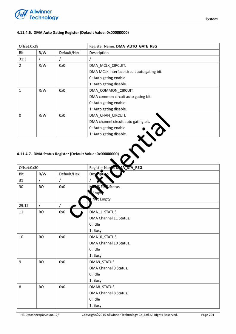
System
H3 Datasheet(Revision1.2) Copyright© 2015 Allwinner Technology Co.,Ltd.All Rights Reserved. Page 201
4.11.4.6. DMA Auto Gating Register (Default Value: 0x00000000)
Offset:0x28 Register Name: DMA_AUTO_GATE_REG
Bit R/W Default/Hex Description
31:3 / / /
2 R/W 0x0 DMA_MCLK_CIRCUIT.
DMA MCLK interface circuit auto gating bit.
0: Auto gating enable
1: Auto gating disable.
1 R/W 0x0 DMA_COMMON_CIRCUIT.
DMA common circuit auto gating bit.
0: Auto gating enable
1: Auto gating disable.
0 R/W 0x0 DMA_CHAN_CIRCUIT.
DMA channel circuit auto gating bit.
0: Auto gating enable
1: Auto gating disable.
4.11.4.7. DMA Status Register (Default Value: 0x00000000)
Offset:0x30 Register Name: DMA_STA_REG
Bit R/W Default/Hex Description
31 / / /
30 RO 0x0 MBUS FIFO Status
0:Empty
1:Not Empty
29:12 / / /
11 RO 0x0 DMA11_STATUS
DMA Channel 11 Status.
0: Idle
1: Busy
10 RO 0x0 DMA10_STATUS
DMA Channel 10 Status.
0: Idle
1: Busy
9 RO 0x0 DMA9_STATUS
DMA Channel 9 Status.
0: Idle
1: Busy
8 RO 0x0 DMA8_STATUS
DMA Channel 8 Status.
0: Idle
1: Busy
confid
ential
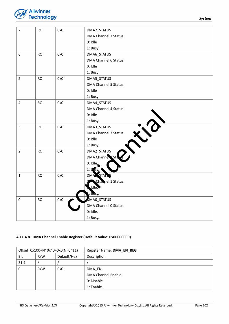
System
H3 Datasheet(Revision1.2) Copyright© 2015 Allwinner Technology Co.,Ltd.All Rights Reserved. Page 202
7 RO 0x0 DMA7_STATUS
DMA Channel 7 Status.
0: Idle
1: Busy
6 RO 0x0 DMA6_STATUS
DMA Channel 6 Status.
0: Idle
1: Busy
5 RO 0x0 DMA5_STATUS
DMA Channel 5 Status.
0: Idle
1: Busy
4 RO 0x0 DMA4_STATUS
DMA Channel 4 Status.
0: Idle
1: Busy.
3 RO 0x0 DMA3_STATUS
DMA Channel 3 Status.
0: Idle
1: Busy.
2 RO 0x0 DMA2_STATUS
DMA Channel 2 Status.
0: Idle,
1: Busy.
1 RO 0x0 DMA1_STATUS
DMA Channel 1 Status.
0: Idle,
1: Busy.
0 RO 0x0 DMA0_STATUS
DMA Channel 0 Status.
0: Idle,
1: Busy.
4.11.4.8. DMA Channel Enable Register (Default Value: 0x00000000)
Offset: 0x100+N*0x40+0x0(N=0~11) Register Name: DMA_EN_REG
Bit R/W Default/Hex Description
31:1 / / /
0 R/W 0x0 DMA_EN.
DMA Channel Enable
0: Disable
1: Enable.
confid
ential

System
H3 Datasheet(Revision1.2) Copyright© 2015 Allwinner Technology Co.,Ltd.All Rights Reserved. Page 203
4.11.4.9. DMA Channel Pause Register (Default Value: 0x00000000)
Offset: 0x100+N*0x40+0x4(N=0~11) Register Name: DMA_PAU_REG
Bit R/W Default/Hex Description
31:1 / / /
0 R/W 0x0 DMA_PAUSE.
Pausing DMA Channel Transfer Data.
0: Resume Transferring,
1: Pause Transferring.
4.11.4.10. DMA Channel Descriptor Address Register (Default Value: 0x00000000)
Offset: 0x100+N*0x40+0x8(N=0~11) Register Name: DMA_DESC_ADDR_REG
Bit R/W Default/Hex Description
31:0 R/W 0x0 DMA_DESC_ADDR
DMA Channel Descriptor Address.
The Descriptor Address must be word-aligned.
4.11.4.11. DMA Channel Configuration Register (Default Value: 0x00000000)
Offset: 0x100+N*0x40+0xC(N=0~11) Register Name: DMA_CFG_REG
Bit R/W Default/Hex Description
31:27 / / /
26:25 RO 0x0 DMA_DEST_DATA_WIDTH.
DMA Destination Data Width.
00: 8-bit
01: 16-bit
10: 32-bit
11: 64-bit
24 / / /
23:22 RO 0x0 DMA_DEST_BST_LEN.
DMA Destination Burst Length.
00: 1
01: 4
10: 8
11: 16
21 RO 0x0 DMA_ADDR_MODE.
DMA Destination Address Mode
0x0: Linear Mode
0x1: IO Mode
20:16 RO DMA_DEST_DRQ_TYPE.
DMA Destination DRQ Type
The details in DRQ Type and Port Corresponding Relation.
confid
ential
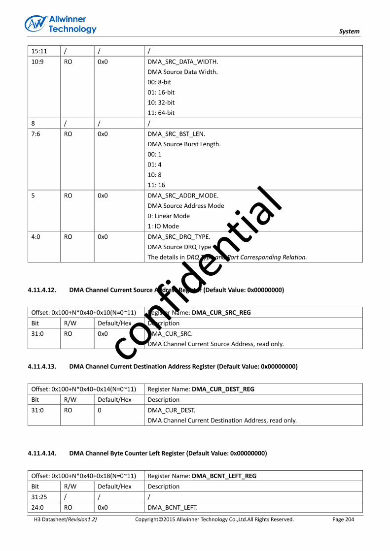
System
H3 Datasheet(Revision1.2) Copyright© 2015 Allwinner Technology Co.,Ltd.All Rights Reserved. Page 204
15:11 / / /
10:9 RO 0x0 DMA_SRC_DATA_WIDTH.
DMA Source Data Width.
00: 8-bit
01: 16-bit
10: 32-bit
11: 64-bit
8 / / /
7:6 RO 0x0 DMA_SRC_BST_LEN.
DMA Source Burst Length.
00: 1
01: 4
10: 8
11: 16
5 RO 0x0 DMA_SRC_ADDR_MODE.
DMA Source Address Mode
0: Linear Mode
1: IO Mode
4:0 RO 0x0 DMA_SRC_DRQ_TYPE.
DMA Source DRQ Type
The details in DRQ Type and Port Corresponding Relation.
4.11.4.12. DMA Channel Current Source Address Register (Default Value: 0x00000000)
Offset: 0x100+N*0x40+0x10(N=0~11) Register Name: DMA_CUR_SRC_REG
Bit R/W Default/Hex Description
31:0 RO 0x0 DMA_CUR_SRC.
DMA Channel Current Source Address, read only.
4.11.4.13. DMA Channel Current Destination Address Register (Default Value: 0x00000000)
Offset: 0x100+N*0x40+0x14(N=0~11) Register Name: DMA_CUR_DEST_REG
Bit R/W Default/Hex Description
31:0 RO 0 DMA_CUR_DEST.
DMA Channel Current Destination Address, read only.
4.11.4.14. DMA Channel Byte Counter Left Register (Default Value: 0x00000000)
Offset: 0x100+N*0x40+0x18(N=0~11) Register Name: DMA_BCNT_LEFT_REG
Bit R/W Default/Hex Description
31:25 / / /
24:0 RO 0x0 DMA_BCNT_LEFT.
confid
ential
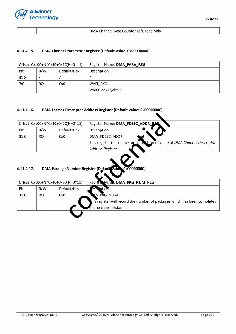
System
H3 Datasheet(Revision1.2) Copyright© 2015 Allwinner Technology Co.,Ltd.All Rights Reserved. Page 205
DMA Channel Byte Counter Left, read only.
4.11.4.15. DMA Channel Parameter Register (Default Value: 0x00000000)
Offset: 0x100+N*0x40+0x1C(N=0~11) Register Name: DMA_PARA_REG
Bit R/W Default/Hex Description
31:8 / / /
7:0 RO 0x0 WAIT_CYC.
Wait Clock Cycles n.
4.11.4.16. DMA Former Descriptor Address Register (Default Value: 0x00000000)
Offset: 0x100+N*0x40+0x2C(N=0~11) Register Name: DMA_FDESC_ADDR_REG
Bit R/W Default/Hex Description
31:0 RO 0x0 DMA_FDESC_ADDR.
This register is used to storing the former value of DMA Channel Descriptor
Address Register.
4.11.4.17. DMA Package Number Register (Default Value: 0x00000000)
Offset: 0x100+N*0x40+0x30(N=0~11) Register Name: DMA_PKG_NUM_REG
Bit R/W Default/Hex Description
31:0 RO 0x0 DMA_PKG_NUM.
This register will record the number of packages which has been completed
in one transmission.
confid
ential
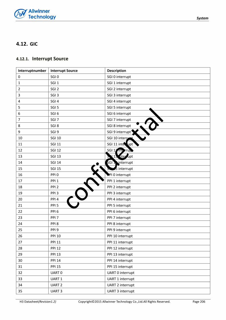
System
H3 Datasheet(Revision1.2) Copyright© 2015 Allwinner Technology Co.,Ltd.All Rights Reserved. Page 206
4.12. GIC
4.12.1. Interrupt Source
Interruptnumber Interrupt Source Description
0 SGI 0 SGI 0 interrupt
1 SGI 1 SGI 1 interrupt
2 SGI 2 SGI 2 interrupt
3 SGI 3 SGI 3 interrupt
4 SGI 4 SGI 4 interrupt
5 SGI 5 SGI 5 interrupt
6 SGI 6 SGI 6 interrupt
7 SGI 7 SGI 7 interrupt
8 SGI 8 SGI 8 interrupt
9 SGI 9 SGI 9 interrupt
10 SGI 10 SGI 10 interrupt
11 SGI 11 SGI 11 interrupt
12 SGI 12 SGI 12 interrupt
13 SGI 13 SGI 13 interrupt
14 SGI 14 SGI 14 interrupt
15 SGI 15 SGI 15 interrupt
16 PPI 0 PPI 0 interrupt
17 PPI 1 PPI 1 interrupt
18 PPI 2 PPI 2 interrupt
19 PPI 3 PPI 3 interrupt
20 PPI 4 PPI 4 interrupt
21 PPI 5 PPI 5 interrupt
22 PPI 6 PPI 6 interrupt
23 PPI 7 PPI 7 interrupt
24 PPI 8 PPI 8 interrupt
25 PPI 9 PPI 9 interrupt
26 PPI 10 PPI 10 interrupt
27 PPI 11 PPI 11 interrupt
28 PPI 12 PPI 12 interrupt
29 PPI 13 PPI 13 interrupt
30 PPI 14 PPI 14 interrupt
31 PPI 15 PPI 15 interrupt
32 UART 0 UART 0 interrupt
33 UART 1 UART 1 interrupt
34 UART 2 UART 2 interrupt
35 UART 3 UART 3 interrupt
confid
ential

System
H3 Datasheet(Revision1.2) Copyright© 2015 Allwinner Technology Co.,Ltd.All Rights Reserved. Page 207
36 / /
37 / /
38 TWI 0 TWI 0 interrupt
39 TWI 1 TWI 1 interrupt
40 TWI 2 TWI 2 interrupt
41 / /
42 / /
43 PA_EINT PA interrupt
44 OWA OWA interrupt
45 I2S/PCM-0 I2S/PCM-0 interrupt
46 I2S/PCM-1 I2S/PCM-1 interrupt
47 I2S/PCM-2 I2S/PCM-2 interrupt
48 / /
49 PG_EINT PG_EINT interrupt
50 Timer 0 Timer 0 interrupt
51 Timer 1 Timer 1 interrupt
52 / /
53 / /
54 / /
55 / /
56 / /
57 Watchdog Watchdog interrupt
58 / /
59 / /
60 / /
61 Audio Codec Audio Codec interrupt
62 KEYADC KEYADC interrupt
63 THS Thermal Sensor interrupt
64 External NMI External Non-Mask Interrupt
65 R_timer 0 R_timer 0 interrupt
66 R_timer 1 R_timer 1 interrupt
67 / /
68 R_watchdog R_watchdog interrupt
69 R_CIR-RX R_CIR-RX interrupt
70 R_UART R_UART interrupt
71 / /
72 R_Alarm 0 R_Alarm 0 interrupt
73 R_Alarm 1 R_Alarm 1 interrupt
74 R_timer 2 R_timer 2 interrupt
75 R_timer 3 R_timer 3 interrupt
76 R_TWI R_TWI interrupt
77 R_PL_EINT R_PL_EINT interrupt
78 R_TWD R_TWD interrupt
79 / /
confid
ential

System
H3 Datasheet(Revision1.2) Copyright© 2015 Allwinner Technology Co.,Ltd.All Rights Reserved. Page 208
80 / /
81 M-box M-box interrupt
82 DMA DMA channel interrupt
83 HS Timer HS Timer interrupt
84 / /
85 / /
86 / /
87 / /
88 SMC SMC interrupt
89 / /
90 VE VE interrupt
91 / /
92 SD/MMC 0 SD/MMC Host Controller 0 interrupt
93 SD/MMC 1 SD/MMC Host Controller 1 interrupt
94 SD/MMC 2 SD/MMC Host Controller 2 interrupt
95 / /
96 / /
97 SPI 0 SPI 0 interrupt
98 SPI 1 SPI 1 interrupt
99 / /
100 / /
101 / /
102 NAND NAND Flash Controller interrupt
103 USB-OTG_Device USB-OTG_Device interrupt
104 USB-OTG_EHCI0 USB-OTG_EHCI0 interrupt
105 USB-OTG_OHCI0 USB-OTG_OHCI0 interrupt
106 USB-EHCI1 USB-EHCI1 interrupt
107 USB-OHCI1 USB-OHCI1 interrupt
108 USB-EHCI2 USB-EHCI2 interrupt
109 USB-OHCI2 USB-OHCI2 interrupt
110 USB-EHCI3 USB-EHCI3 interrupt
111 USB-OHCI3 USB-OHCI3 interrupt
112 SS_S SS_S interrupt
113 TS TS interrupt
114 EMAC EMAC interrupt
115 SCR SCR interrupt
116 CSI CSI interrupt
117 CSI_CCI CSI_CCI interrupt
118 LCD0 LCD0 Controller interrupt
119 LCD1 LCD1 Controller interrupt
120 HDMI HDMI interrupt
121 / /
122 / /
123 / /
confid
ential

System
H3 Datasheet(Revision1.2) Copyright© 2015 Allwinner Technology Co.,Ltd.All Rights Reserved. Page 209
124 TVE TVE interrupt
125 DIT DIT interrupt
126 SS_NS SS_NS interrupt
127 DE DE interrupt
128 / /
129 GPU-GP GPU-GP interrupt
130 GPU-GPMMU GPU-GPMMU interrupt
131 GPU-PP0 GPU-PP0 interrupt
132 GPU-PPMMU0 GPU-PPMMU0 interrupt
133 GPU-PMU GPU-PMU interrupt
134 GPU-PP1 GPU-PP1 interrupt
135 GPU-PPMMU1 GPU-PPMMU1 interrupt
136 / /
137 / /
138 / /
139 / /
140 CTI0 CTI0 interrupt
141 CTI1 CTI1 interrupt
142 CTI2 CTI2 interrupt
143 CTI3 CTI3 interrupt
144 COMMTX0 COMMTX0 interrupt
145 COMMTX1 COMMTX1 interrupt
146 COMMTX2 COMMTX2 interrupt
147 COMMTX3 COMMTX3 interrupt
148 COMMRX0 COMMRX0 interrupt
159 COMMRX1 COMMRX1 interrupt
150 COMMRX2 COMMRX2 interrupt
151 COMMRX3 COMMRX3 interrupt
152 PMU0 PMU0 interrupt
153 PMU1 PMU1 interrupt
154 PMU2 PMU2 interrupt
155 PMU3 PMU3 interrupt
156 AXI_ERROR AXI_ERROR interrupt
Note:For details about GIC,please refer to the GIC PL400 technical reference manual and ARM GIC Architecture
Specification V2.0.
confid
ential

System
H3 Datasheet(Revision1.2) Copyright© 2015 Allwinner Technology Co.,Ltd.All Rights Reserved. Page 210
4.13. Message Box
4.13.1. Overview
Message Box provides an MSGBox-interrupt mechanism for on-chip processors intercommunication.
The MSGBox-interrupt mechanism allows the software to establish a communication channel between the two users
through a set of registers and associated interrupt signals by sending or receiving messages.
The Message Box includes the following features:
• Two users for Message Box instance(User0 for CPUS and User1 for CPU0/CPU1)
• Eight Message Queues for the MSGBox instance
• Each of Queues could be configured as transmitter or receiver for user
• Two interrupts (one per user ) for the MSGBox instance
• Register polling for the MSGBox instance
• 32-bit message width
• Four-message FIFO depth for Each message queue
4.13.2. Functionalities Description
confid
ential
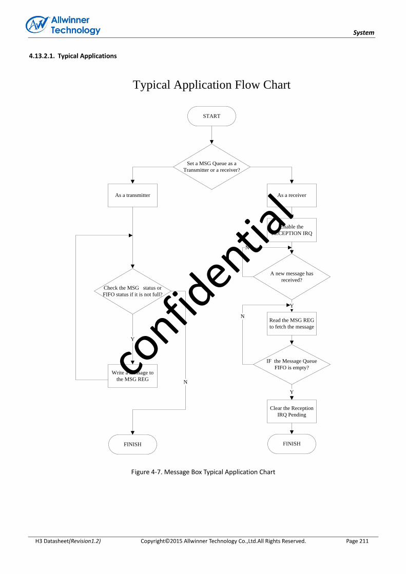
System
H3 Datasheet(Revision1.2) Copyright© 2015 Allwinner Technology Co.,Ltd.All Rights Reserved. Page 211
4.13.2.1. Typical Applications
Typical Application Flow Chart
Set a MSG Queue as a
Transmitter or a receiver?
START
FINISH
Check the MSG status or
FIFO status if it is not full?
Write a message to
the MSG REG
As a transmitter As a receiver
Enable the
RECEPTION IRQ
A new message has
received?
Read the MSG REG
to fetch the message
FINISH
Clear the Reception
IRQ Pending
Y
Y
N
N
IF the Message Queue
FIFO is empty?
Y
N
Figure 4-7. Message Box Typical Application Chart
confid
ential

System
H3 Datasheet(Revision1.2) Copyright© 2015 Allwinner Technology Co.,Ltd.All Rights Reserved. Page 212
4.13.2.2. Functional Block Diagram
MSGBOX_MSG_REG_M
MSGBOX_MSG_STATUS_REG_M
MSGBOX_FIFO_STATUS_REG_M
MSGBox Message Queue m (m : from 0 to 7)
MSGBox
USER0 USER1
MSGBOX_IRQ_EN_REG_0
MSGBOX_IRQ_STATUS_REG_0
For user0
MSGBOX_CTRL_REG0
MSGBOX_IRQ_EN_REG_1
MSGBOX_IRQ_STATUS_REG_1
For user1
MSGBOX_CTRL_REG1
Four Message FIFO
Figure 4-8. Message Box Functional Block Diagram
4.13.3. Operation Principle
4.13.3.1. Message Queue Assignment
To transmit messages from a user to the other user through any Message Queue, set the corresponding bit in the
MSGBOX_CTRL_REG0/MSGBOX_CTRL_REG1 register.
When a 32-bit message is written to the MSGBOX_MSG_REG_M register, the message is appended into the FIFO queue.
This queue holds 4 messages. If the queue is full, the message is discarded. The receiver user could read the
MSGBOX_MSG_REG_M (m is the message queue number, where m=0 to 7) register to retrieve a message from the
corresponding Message Queue FIFO.
It is recommended that register polling be used for a user to send a message:
confid
ential

System
H3 Datasheet(Revision1.2) Copyright© 2015 Allwinner Technology Co.,Ltd.All Rights Reserved. Page 213
• Set a Message Queue as a transmitter (in the MSGBOX_CTRL_REG0/1).
• Check the FIFO status or the message status (in the MSGBOX_FIFO_STATUS_REG_M or MSGBOX_MSG_ STATUS_
REG_M).
• Write the message to the corresponding MSGBOX_MSG_REG_M register, if space is available.
The transmit interrupt might be used when the initial MSGBox status indicates that the Message Queue is full. In this
case, the sender can enable the corresponding MSGBOX_IRQ_EN_REG_U interrupt for the user. This allows the user to
be notified by interrupt when the message queue is not full.
4.13.3.2. Interrupt request
An interrupt request allows the user of the MSGBox to be notified when a new message is received or when the
message queue is not full.
An event can generate an interrupt request when enable the corresponding bit in the MSGBOX_IRQ_EN_REG_U (u is
the user number, where u=0 or 1) register. Events are reported in the appropriate MSGBOX_IRQ_STATUS_REG_U
register.
An event stops generating interrupt requests when disable the corresponding bit in the MSGBOX_IRQ_EN_REG_U
register.
In case of the MSGBOX_IRQ_STATUS_REG_U register, the event is reported in the corresponding bit even if the
interrupt request generation is disabled for this event.
4.13.4. Message Box Register List
Module Name Base Address
MSGBOX 0x01C17000
Register Name Offset Description
MSGBOX_CTRL_REG0 0x0000 Message Queue Attribute Control Register 0
MSGBOX_CTRL_REG1 0x0004 Message Queue Attribute Control Register 1
MSGBOXU_IRQ_EN_REG 0x0040+n*0x20 IRQ Enable For User N(N=0,1)
MSGBOXU_IRQ_STATUS_REG 0x0050+n*0x20 IRQ Status For User N(N=0,1)
MSGBOXM_FIFO_STATUS_REG 0x0100+N*0x4 FIFO Status For Message Queue N(N = 0~7)
MSGBOXM_MSG_STATUS_REG 0x0140+N*0x4 Message Status For Message Queue N(N=0~7)
MSGBOXM_MSG_REG 0x0180+N*0x4 Message Register For Message Queue N(N=0~7)
confid
ential

System
H3 Datasheet(Revision1.2) Copyright© 2015 Allwinner Technology Co.,Ltd.All Rights Reserved. Page 214
4.13.5. Message Box Register Description
4.13.5.1. MSGBox Control Register 0(Default Value: 0x10101010)
Offset: 0x00 Register Name: MSGBOX_CTRL_REG0
Bit R/W Default/Hex Description
31:29 / / /
28 R/W 0x1 TRANSMIT_MQ3.
Message Queue 3 is a Transmitter of user u.
0: user0
1: user1
27:25 / / /
24 R/W 0x0 RECEPTION_MQ3.
Message Queue 3 is a Receiver of user u.
0: user0
1: user1
23:21 / / /
20 R/W 0x1 TRANSMIT_MQ2.
Message Queue 2 is a Transmitter of user u.
0: user0
1: user1
19:17 / / /
16 R/W 0x0 RECEPTION_MQ2.
Message Queue 2 is a Receiver of user u.
0: user0
1: user1
15:13 / / /
12 R/W 0x1 TRANSMIT_MQ1
Message Queue 1 is a Transmitter of user u.
0: user0
1: user1
11:9 / / /
8 R/W 0x0 RECEPTION_MQ1.
Message Queue 1 is a Receiver of user u.
0: user0
1: user1
7:5 / / /
4 R/W 0x1 TRANSMIT_MQ0.
Message Queue 0 is a Transmitter of user u.
0: user0
1: user1
3:1 / / /
0 R/W 0x0 RECEPTION_MQ0.
Message Queue 0 is a Receiver of user u.
confid
ential
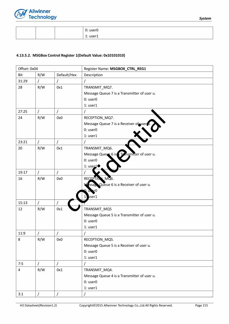
System
H3 Datasheet(Revision1.2) Copyright© 2015 Allwinner Technology Co.,Ltd.All Rights Reserved. Page 215
0: user0
1: user1
4.13.5.2. MSGBox Control Register 1(Default Value: 0x10101010)
Offset: 0x04 Register Name: MSGBOX_CTRL_REG1
Bit R/W Default/Hex Description
31:29 / / /
28 R/W 0x1 TRANSMIT_MQ7.
Message Queue 7 is a Transmitter of user u.
0: user0
1: user1
27:25 / / /
24 R/W 0x0 RECEPTION_MQ7.
Message Queue 7 is a Receiver of user u.
0: user0
1: user1
23:21 / / /
20 R/W 0x1 TRANSMIT_MQ6.
Message Queue 6 is a Transmitter of user u.
0: user0
1: user1
19:17 / / /
16 R/W 0x0 RECEPTION_MQ6.
Message Queue 6 is a Receiver of user u.
0: user0
1: user1
15:13 / / /
12 R/W 0x1 TRANSMIT_MQ5
Message Queue 5 is a Transmitter of user u.
0: user0
1: user1
11:9 / / /
8 R/W 0x0 RECEPTION_MQ5.
Message Queue 5 is a Receiver of user u.
0: user0
1: user1
7:5 / / /
4 R/W 0x1 TRANSMIT_MQ4.
Message Queue 4 is a Transmitter of user u.
0: user0
1: user1
3:1 / / /
confid
ential

System
H3 Datasheet(Revision1.2) Copyright© 2015 Allwinner Technology Co.,Ltd.All Rights Reserved. Page 216
0 R/W 0x0 RECEPTION_MQ4.
Message Queue 4 is a Receiver of user u.
0: user0
1: user1
4.13.5.3. MSGBox IRQ Enable Register (Default Value: 0x00000000)
Offset:0x40+N*0x20 (N=0,1) Register Name: MSGBOXU_IRQ_EN_REG
Bit R/W Default/Hex Description
31:16 / / /
15 R/W 0x0 TRANSMIT_MQ7_IRQ_EN.
0: Disable
1: Enable (It will notify user u by interrupt when Message Queue 7 is not
full.)
14 R/W 0x0 RECEPTION_MQ7_IRQ_EN.
0: Disable
1: Enable (It will notify user u by interrupt when Message Queue 7 has
received a new message.)
13 R/W 0x0 TRANSMIT_MQ6_IRQ_EN.
0: Disable
1: Enable (It will Notify user u by interrupt when Message Queue 6 is not
full.)
12 R/W 0x0 RECEPTION_MQ6_IRQ_EN.
0: Disable
1: Enable (It will notify user u by interrupt when Message Queue 6 has
received a new message.)
11 R/W 0x0 TRANSMIT_MQ5_IRQ_EN.
0: Disable
1: Enable (It will notify user u by interrupt when Message Queue 5 is not
full.)
10 R/W 0x0 RECEPTION_MQ5_IRQ_EN.
0: Disable
1: Enable (It will notify user u by interrupt when Message Queue 5 has
received a new message.)
9 R/W 0x0 TRANSMIT_MQ4_IRQ_EN.
0: Disable
1: Enable (It will notify user u by interrupt when Message Queue 4 is not
full.)
8 R/W 0x0 RECEPTION_MQ4_IRQ_EN.
0: Disable
1: Enable (It will notify user u by interrupt when Message Queue 4 has
received a new message.)
7 R/W 0x0 TRANSMIT_MQ3_IRQ_EN.
0: Disable
confid
ential

System
H3 Datasheet(Revision1.2) Copyright© 2015 Allwinner Technology Co.,Ltd.All Rights Reserved. Page 217
1: Enable (It will notify user u by interrupt when Message Queue 3 is not
full.)
6 R/W 0x0 RECEPTION_MQ3_IRQ_EN.
0: Disable
1: Enable (It will notify user u by interrupt when Message Queue 3 has
received a new message.)
5 R/W 0x0 TRANSMIT_MQ2_IRQ_EN.
0: Disable
1: Enable (It will notify user u by interrupt when Message Queue 2 is not
full.)
4 R/W 0x0 RECEPTION_MQ2_IRQ_EN.
0: Disable
1: Enable (It will notify user u by interrupt when Message Queue 2 has
received a new message.)
3 R/W 0x0 TRANSMIT_MQ1_IRQ_EN.
0: Disable
1: Enable (It will notify user u by interrupt when Message Queue 1 is not
full.)
2 R/W 0x0 RECEPTION_MQ1_IRQ_EN.
0: Disable
1: Enable (It will notify user u by interrupt when Message Queue 1 has
received a new message.)
1 R/W 0x0 TRANSMIT_MQ0_IRQ_EN.
0: Disable
1: Enable (It will notify user u by interrupt when Message Queue 0 is not
full.)
0 R/W 0x0 RECEPTION_MQ0_IRQ_EN.
0: Disable
1: Enable (It will notify user u by interrupt when Message Queue 0 has
received a new message.)
4.13.5.4. MSGBox IRQ Status Register u(Default Value: 0x0000AAAA)
Offset:0x50+N*0x20 (N=0,1) Register Name: MSGBOXU_IRQ_STATUS_REG
Bit R/W Default/Hex Description
31:16 / / /
15 R/W 0x1 TRANSMIT_MQ7_IRQ_PEND.
0: No effect,
1: Pending. This bit will be pending for user u when Message Queue 7 is not
full. Set one to this bit will clear it.
14 R/W 0x0 RECEPTION_MQ7_IRQ_PEND.
0: No effect,
1: Pending. This bit will be pending for user u when Message Queue 7 has
received a new message. Set one to this bit will clear it.
confid
ential

System
H3 Datasheet(Revision1.2) Copyright© 2015 Allwinner Technology Co.,Ltd.All Rights Reserved. Page 218
13 R/W 0x1 TRANSMIT_MQ6_IRQ_PEND.
0: No effect,
1: Pending. This bit will be pending for user u when Message Queue 6 is not
full. Set one to this bit will clear it.
12 R/W 0x0 RECEPTION_MQ6_IRQ_PEND.
0: No effect,
1: Pending. This bit will be pending for user u when Message Queue 6 has
received a new message. Set one to this bit will clear it.
11 R/W 0x1 TRANSMIT_MQ5_IRQ_PEND.
0: No effect,
1: Pending. This bit will be pending for user u when Message Queue 5 is not
full. Set one to this bit will clear it.
10 R/W 0x0 RECEPTION_MQ5_IRQ_PEND.
0: No effect,
1: Pending. This bit will be pending for user u when Message Queue 5 has
received a new message. Set one to this bit will clear it.
9 R/W 0x1 TRANSMIT_MQ4_IRQ_PEND.
0: No effect,
1: Pending. This bit will be pending for user u when Message Queue 4 is not
full. Set one to this bit will clear it.
8 R/W 0x0 RECEPTION_MQ4_IRQ_PEND.
0: No effect,
1: Pending. This bit will be pending for user u when Message Queue 4 has
received a new message. Set one to this bit will clear it.
7 R/W 0x1 TRANSMIT_MQ3_IRQ_PEND.
0: No effect,
1: Pending. This bit will be pending for user u when Message Queue 3 is not
full. Set one to this bit will clear it.
6 R/W 0x0 RECEPTION_MQ3_IRQ_PEND.
0: No effect,
1: Pending. This bit will be pending for user u when Message Queue 3 has
received a new message. Set one to this bit will clear it.
5 R/W 0x1 TRANSMIT_MQ2_IRQ_PEND.
0: No effect,
1: Pending. This bit will be pending for user u when Message Queue 2 is not
full. Set one to this bit will clear it.
4 R/W 0x0 RECEPTION_MQ2_IRQ_PEND.
0: No effect,
1: Pending. This bit will be pending for user u when Message Queue 2 has
received a new message. Set one to this bit will clear it.
3 R/W 0x1 TRANSMIT_MQ1_IRQ_PEND.
0: No effect,
1: Pending. This bit will be pending for user u when Message Queue 1 is not
full. Set one to this bit will clear it.
2 R/W 0x0 RECEPTION_MQ1_IRQ_PEND.
confid
ential
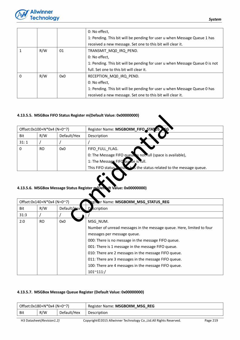
System
H3 Datasheet(Revision1.2) Copyright© 2015 Allwinner Technology Co.,Ltd.All Rights Reserved. Page 219
0: No effect,
1: Pending. This bit will be pending for user u when Message Queue 1 has
received a new message. Set one to this bit will clear it.
1 R/W 01 TRANSMIT_MQ0_IRQ_PEND.
0: No effect,
1: Pending. This bit will be pending for user u when Message Queue 0 is not
full. Set one to this bit will clear it.
0 R/W 0x0 RECEPTION_MQ0_IRQ_PEND.
0: No effect,
1: Pending. This bit will be pending for user u when Message Queue 0 has
received a new message. Set one to this bit will clear it.
4.13.5.5. MSGBox FIFO Status Register m(Default Value: 0x00000000)
Offset:0x100+N*0x4 (N=0~7) Register Name: MSGBOXM_FIFO_STATUS_REG
Bit R/W Default/Hex Description
31: 1 / / /
0 RO 0x0 FIFO_FULL_FLAG.
0: The Message FIFO queue is not full (space is available),
1: The Message FIFO queue is full.
This FIFO status register has the status related to the message queue.
4.13.5.6. MSGBox Message Status Register m(Default Value: 0x00000000)
Offset:0x140+N*0x4 (N=0~7) Register Name: MSGBOXM_MSG_STATUS_REG
Bit R/W Default/Hex Description
31:3 / / /
2:0 RO 0x0 MSG_NUM.
Number of unread messages in the message queue. Here, limited to four
messages per message queue.
000: There is no message in the message FIFO queue.
001: There is 1 message in the message FIFO queue.
010: There are 2 messages in the message FIFO queue.
011: There are 3 messages in the message FIFO queue.
100: There are 4 messages in the message FIFO queue.
101~111:/
4.13.5.7. MSGBox Message Queue Register (Default Value: 0x00000000)
Offset:0x180+N*0x4 (N=0~7) Register Name: MSGBOXM_MSG_REG
Bit R/W Default/Hex Description
confid
ential

System
H3 Datasheet(Revision1.2) Copyright© 2015 Allwinner Technology Co.,Ltd.All Rights Reserved. Page 220
31:0 R/W 0x0 The message register stores the next to be read message of the message FIFO
queue. Reads remove the message from the FIFO queue.
confid
ential

System
H3 Datasheet(Revision1.2) Copyright© 2015 Allwinner Technology Co.,Ltd.All Rights Reserved. Page 221
4.14. Spinlock
4.14.1. Overview
Spinlock provides hardware assistance for synchronizing the processes running on multiple processors in the device.
The SpinLock module implements thirty-two 32-bit spinlocks (or hardware semaphores), which provide an efficient way
to perform a lock operation of a device resource using a single read access, thus avoiding the need for a
‘read-modify-write’ bus transfer that not all the programmable cores are capable of.
Spinlocks are present to solve the need for synchronization and mutual exclusion between heterogeneous processors
and those not operating under a single, shared operating system. There is no alternative mechanism to accomplish
these operations between processors in separate subsystems. However, Spinlocks do not solve all system
synchronization issues. They have limited applicability and should be used with care to implement higher level
synchronization protocols.
A spinlock is appropriate for mutual exclusion for access to a shared data structure. It should be used only when:
1) The time to hold the lock is predictable and small (for example, a maximum hold time of less than 200 CPU cycles
may be acceptable).
2) The locking task cannot be preempted, suspended, or interrupted while holding the lock (this would make the hold
time large and unpredictable).
3) The lock is lightly contended, that is the chance of any other process (or processor) trying to acquire the lock while
it is held is small.
If the conditions are not met, then a spinlock is not a good candidate. One alternative is to use a spinlock for critical
section control (engineered to meet the conditions) to implement a higher level semaphore that can support
preemption, notification, timeout or other higher level properties.
The Spinlock includes the following features:
• Spinlock module includes 32 spinlocks
• Two kinds of status of lock register: TAKEN and NOT TAKEN
confid
ential
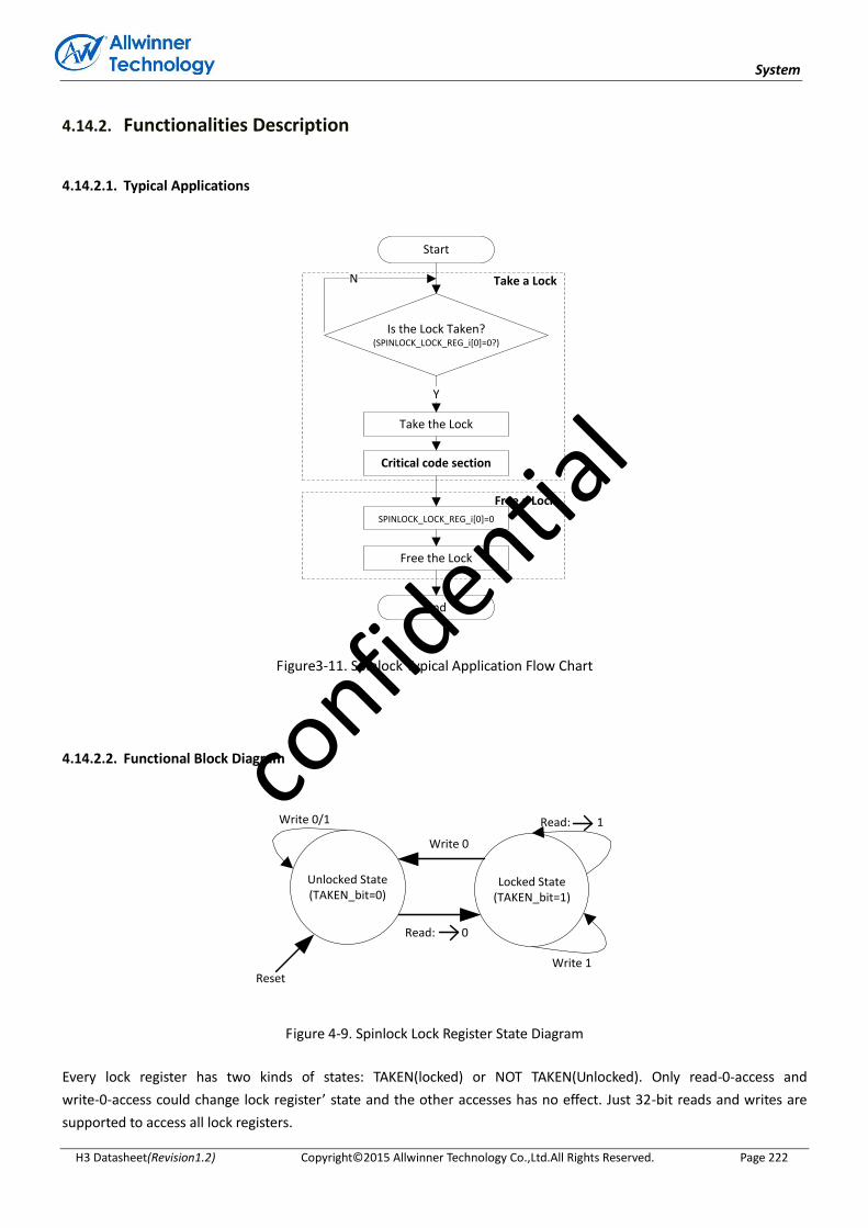
System
H3 Datasheet(Revision1.2) Copyright© 2015 Allwinner Technology Co.,Ltd.All Rights Reserved. Page 222
4.14.2. Functionalities Description
4.14.2.1. Typical Applications
Start
Is the Lock Taken?(SPINLOCK_LOCK_REG_i[0]=0?)
SPINLOCK_LOCK_REG_i[0]=0
End
Y
N Take a Lock
Free a Lock
Take the Lock
Critical code section
Free the Lock
Figure3-11. Spinlock Typical Application Flow Chart
4.14.2.2. Functional Block Diagram
Unlocked State(TAKEN_bit=0)
Locked State(TAKEN_bit=1)
Read: 0
Write 1
Read: 1
Write 0
Write 0/1
Reset
Figure 4-9. Spinlock Lock Register State Diagram
Every lock register has two kinds of states: TAKEN(locked) or NOT TAKEN(Unlocked). Only read-0-access and
write-0-access could change lock register’ state and the other accesses has no effect. Just 32-bit reads and writes are
supported to access all lock registers.
confid
ential
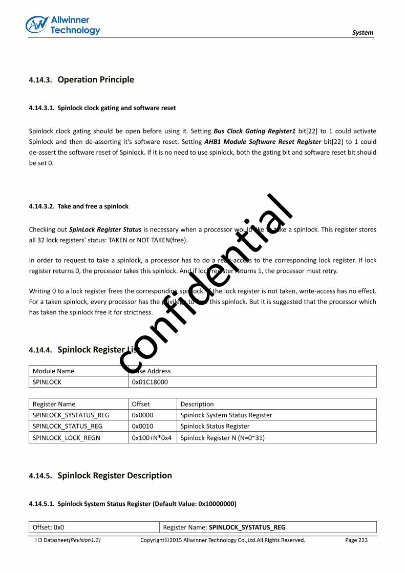
System
H3 Datasheet(Revision1.2) Copyright© 2015 Allwinner Technology Co.,Ltd.All Rights Reserved. Page 223
4.14.3. Operation Principle
4.14.3.1. Spinlock clock gating and software reset
Spinlock clock gating should be open before using it. Setting Bus Clock Gating Register1 bit[22] to 1 could activate
Spinlock and then de-asserting it's software reset. Setting AHB1 Module Software Reset Register bit[22] to 1 could
de-assert the software reset of Spinlock. If it is no need to use spinlock, both the gating bit and software reset bit should
be set 0.
4.14.3.2. Take and free a spinlock
Checking out SpinLock Register Status is necessary when a processor would like to take a spinlock. This register stores
all 32 lock registers’ status: TAKEN or NOT TAKEN(free).
In order to request to take a spinlock, a processor has to do a read-access to the corresponding lock register. If lock
register returns 0, the processor takes this spinlock. And if lock register returns 1, the processor must retry.
Writing 0 to a lock register frees the corresponding spinlock. If the lock register is not taken, write-access has no effect.
For a taken spinlock, every processor has the privilege to free this spinlock. But it is suggested that the processor which
has taken the spinlock free it for strictness.
4.14.4. Spinlock Register List
Module Name Base Address
SPINLOCK 0x01C18000
Register Name Offset Description
SPINLOCK_SYSTATUS_REG 0x0000 Spinlock System Status Register
SPINLOCK_STATUS_REG 0x0010 Spinlock Status Register
SPINLOCK_LOCK_REGN 0x100+N*0x4 Spinlock Register N (N=0~31)
4.14.5. Spinlock Register Description
4.14.5.1. Spinlock System Status Register (Default Value: 0x10000000)
Offset: 0x0 Register Name: SPINLOCK_SYSTATUS_REG
confid
ential
System
H3 Datasheet(Revision1.2) Copyright© 2015 Allwinner Technology Co.,Ltd.All Rights Reserved. Page 224
Bit R/W Default/Hex Description
31:30 / / /
29:28 RO 0x1 LOCKS_NUM.
Number of lock registers implemented.
0x1: This instance has 32 lock registers.
0x2: This instance has 64 lock registers.
0x3: This instance has 128 lock registers.
0x4: This instance has 256 lock registers.
27:16 / / /
15:9 / / /
8 RO 0x0 IU0.
In-Use flag0, covering lock register0-31.
0: All lock register 0-31 are in the Not Taken state.
1: At least one of the lock register 0-31 is in the Taken state.
7:0 / / /
4.14.5.2. Spinlock Register Status (Default Value: 0x00000000)
Offset: 0x10 Register Name: SPINLOCK_STATUS_REG
Bit R/W Default/Hex Description
[i]
(i=0~31)
RO 0x0 LOCK_REG_STATUS.
SpinLock[i] status (i=0~31)
0: The Spinlock is free,
1: The Spinlock is taken.
4.14.5.3. Spinlock Register N (N=0 to 31)(Default Value: 0x00000000)
Offset:0x100+N*0x4 (N=0~31) Register Name: SPINLOCKN_LOCK_REG
Bit R/W Default/Hex Description
31:1 / / /
0 R/W 0x0 TAKEN.
Lock State.
Read 0x0: The lock was previously Not Taken (free).The requester is
granted the lock.
Write 0x0: Set the lock to Not Taken (free).
Read 0x1: The lock was previously Taken. The requester is not granted
the lock and must retry.
Write 0x1: No update to the lock value.
confid
ential
System
H3 Datasheet(Revision1.2) Copyright© 2015 Allwinner Technology Co.,Ltd.All Rights Reserved. Page 225
4.14.6. Programming Guidelines
Take CPU0's synchronization with CPUS with Spinlock0 for an example, CPU0 takes the spinlock0 firstly in the instance:
CPU0
Step 1: CPU0 initializes Spinlock
writel(readl(BUS_GATING_REG1)|(1<<22) ,BUS_GATING_REG1); //open Spinlock clock gating
writel (readl(BUS_RST_REG1)|(1<<22) , BUS_RST_REG1); //software reset Spinlock
Step 2: CPU0 requests to take spinlock0
rdata=readl(SPINLOCK_STATUS_REG0); //check lock register0 status, if it is taken, check till
if(rdata != 0) rdata=readl(SPINLOCK_STATUS_REG0); // lock register0 is free
rdata=readl(SPINLOCKN_LOCK_REG0); //request to take spinlock0, if fail, retry till
if(rdata != 0) rdata=readl(SPINLOCKN_LOCK_REG0); // lock register0 is taken
---------- CPU0 critical code section ----------
Step 3: CPU0 free spinlock0
writel (0, SPINLOCKN_LOCK_REG0); //CPU0 frees spinlock0
Step 4: CPU0 waits for CPUS’ freeing spinlock0
writel (readl(SPINLOCK_STATUS_REG0) == 1); // CPU0 waits for CPUS’ freeing spinlock0
CPUS
Step 1: CPU0 has taken spinlock0, CPUS waits for CPU0’ freeing spinlock0
while(readl(SPINLOCK_STATUS_REG0) == 1); // CPUS waits for CPU0’ freeing spinlock0
Step 2: CPUS takes spinlock0 and go on
---------- CPUS critical code section ----------
Step 3: CPUS frees spinlock0
writel (0, SPINLOCKN_LOCK_REG0); //CPUS frees spinlock0
confid
ential
System
H3 Datasheet(Revision1.2) Copyright© 2015 Allwinner Technology Co.,Ltd.All Rights Reserved. Page 226
4.15. Crypto Engine
4.15.1. Overview
The Crypto Engine is one encrypt/ decrypt function accelerator. It is suitable for a variety of applications. It can support
encryption ,decryption and calculate the hash value. Several modes are supported by the Crypto Engine. The Crypto
Engine has a special internal DMA(IDMA) controller to transfer data .
It includes the following features:
Support symmetrical algorithm :AES, DES, TDES
Support secure Hash algorithm: MD5, SHA-1,SHA-224,SHA-256,SHA-384,SHA-512,HMAC-SHA1
Support 160-bits hardware PRNG with 175-bits seed
Support 256-bits hardware TRNG
Support ECB, CBC, CTR modes for DES/TDES
Support ECB, CBC, CTR, CTS,OFB,CFB,CBC-MAC modes for AES
Support 128-bits, 192-bits and 256-bits key size for AES
4.15.2. Functionalities Description
confid
ential
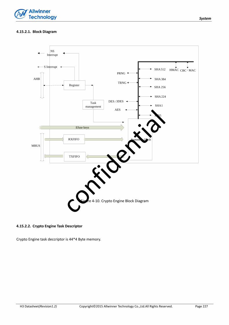
System
H3 Datasheet(Revision1.2) Copyright© 2015 Allwinner Technology Co.,Ltd.All Rights Reserved. Page 227
4.15.2.1. Block Diagram
RXFIFO
TXFIFO
Symmeric/Hash
MBUS
DES / 3DES
AES
SHA1
SHA 224
SHA 256
MD5
TRNG
AHB
Register
PRNG
SHA 384
SHA512 HMAC CBC - MAC
NS
Interrupt
Task
management
Efuse keys
S Interrupt
Figure 4-10. Crypto Engine Block Diagram
4.15.2.2. Crypto Engine Task Descriptor
Crypto Engine task deccriptor is 44*4 Byte memory.
confid
ential

System
H3 Datasheet(Revision1.2) Copyright© 2015 Allwinner Technology Co.,Ltd.All Rights Reserved. Page 228
Task chaining
task chaining id=0common ctl
symmetric ctl
reserved
key descriptor
iv descriptorctr descriptor
data len
src adr0
dst adr7dst len7
next descriptor(task1)
src len0
reserved[3]…………
task0 task1 task2 ………… taskn
src adr7src len7
…dst adr0dst len0
…
task chaining id=0common ctl
symmetric ctl
reserved
key descriptor
iv descriptorctr descriptor
data len
src adr0
dst adr7dst len7
next descriptor(task2)
src len0
reserved[3]
src adr7src len7
…
dst adr0dst len0
…
task chaining id=0common ctl
symmetric ctl
reserved
key descriptor
iv descriptorctr descriptor
data len
src adr0
dst adr7dst len7
next descriptor(taskn)
src len0
reserved[3]
src adr7src len7
…
dst adr0dst len0
…
Figure 4-11. Crypto Engine Task Chaining Block Diagram
task_descriptor_queue common control bitmap(32bit)
Bit Description
31 Each of the tasks to be an interrupt
0:don't interrupt
1:interrupt
29:28 /
27 DMA Read/Write Consistent
0:Send end flag after data write-instruction finished
1:Read data when CE received response of write-instruction ,if write-instruction is non-finished,
waiting until write-instruction finished.
24 /
23:17 MAC Length for CBC-MAC
length=bit[23:17]+1
16 IV_Mode
IV Steady of hash algorithm
0: Constants
1: Arbitrary IV
Notes: It is only used for SHA-1/SHA-224/SHA-256/SHA-384/SHA-512/MD5 engine.
15 HMAC_SHA1_Last_Block_Flag
When set to "1", it means this is the last block for HMAC-SHA1.
14:9 /
8 CE_OP_DIR
CE Operation Direction
0: Encryption
1: Decryption
7 /
confid
ential
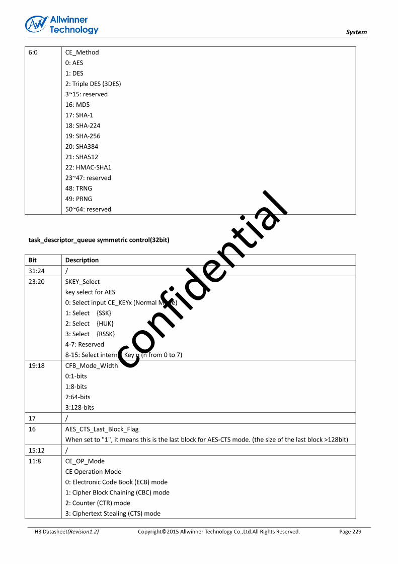
System
H3 Datasheet(Revision1.2) Copyright© 2015 Allwinner Technology Co.,Ltd.All Rights Reserved. Page 229
6:0 CE_Method
0: AES
1: DES
2: Triple DES (3DES)
3~15: reserved
16: MD5
17: SHA-1
18: SHA-224
19: SHA-256
20: SHA384
21: SHA512
22: HMAC-SHA1
23~47: reserved
48: TRNG
49: PRNG
50~64: reserved
task_descriptor_queue symmetric control(32bit)
Bit Description
31:24 /
23:20 SKEY_Select
key select for AES
0: Select input CE_KEYx (Normal Mode)
1: Select {SSK}
2: Select {HUK}
3: Select {RSSK}
4-7: Reserved
8-15: Select internal Key n (n from 0 to 7)
19:18 CFB_Mode_Width
0:1-bits
1:8-bits
2:64-bits
3:128-bits
17 /
16 AES_CTS_Last_Block_Flag
When set to "1", it means this is the last block for AES-CTS mode. (the size of the last block >128bit)
15:12 /
11:8 CE_OP_Mode
CE Operation Mode
0: Electronic Code Book (ECB) mode
1: Cipher Block Chaining (CBC) mode
2: Counter (CTR) mode
3: Ciphertext Stealing (CTS) mode
confid
ential
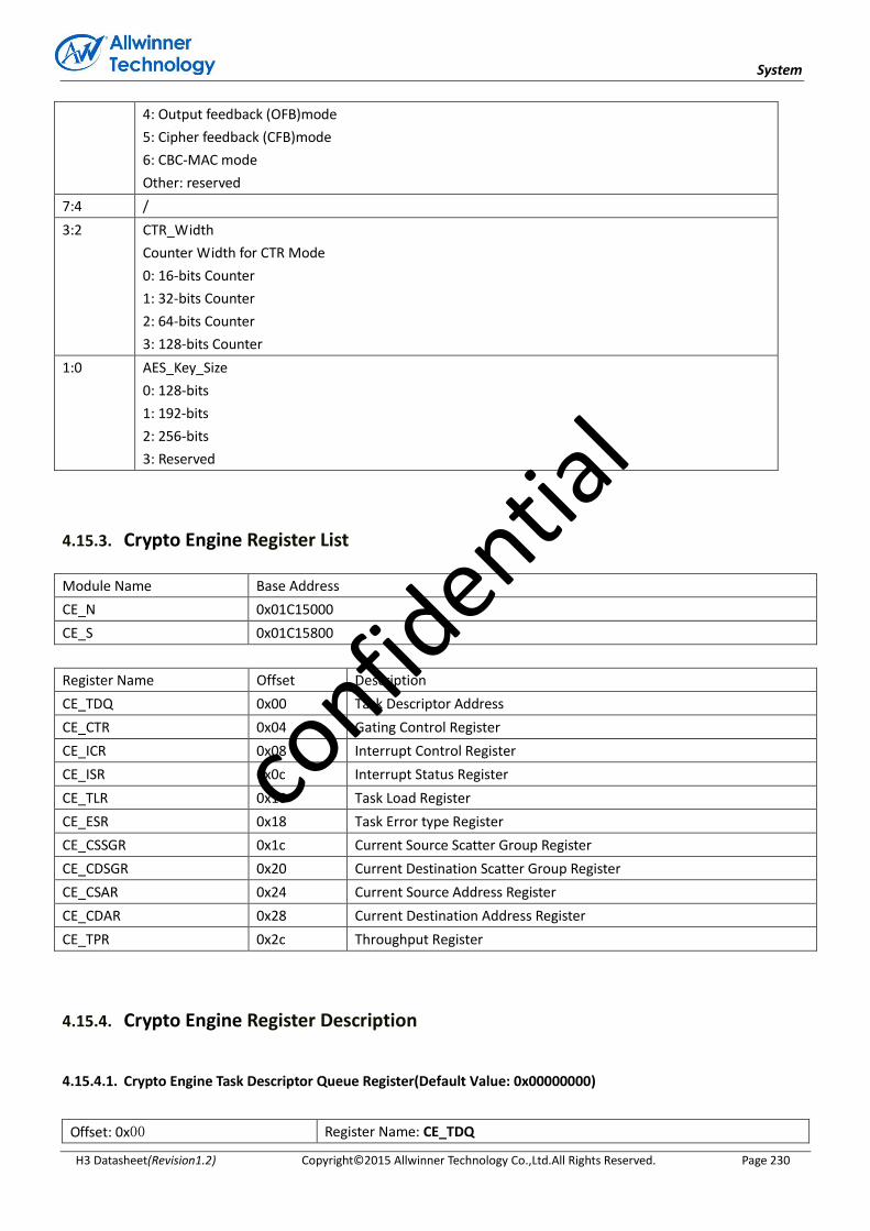
System
H3 Datasheet(Revision1.2) Copyright© 2015 Allwinner Technology Co.,Ltd.All Rights Reserved. Page 230
4: Output feedback (OFB)mode
5: Cipher feedback (CFB)mode
6: CBC-MAC mode
Other: reserved
7:4 /
3:2 CTR_Width
Counter Width for CTR Mode
0: 16-bits Counter
1: 32-bits Counter
2: 64-bits Counter
3: 128-bits Counter
1:0 AES_Key_Size
0: 128-bits
1: 192-bits
2: 256-bits
3: Reserved
4.15.3. Crypto Engine Register List
Module Name Base Address
CE_N 0x01C15000
CE_S 0x01C15800
Register Name Offset Description
CE_TDQ 0x00 Task Descriptor Address
CE_CTR 0x04 Gating Control Register
CE_ICR 0x08 Interrupt Control Register
CE_ISR 0x0c Interrupt Status Register
CE_TLR 0x10 Task Load Register
CE_ESR 0x18 Task Error type Register
CE_CSSGR 0x1c Current Source Scatter Group Register
CE_CDSGR 0x20 Current Destination Scatter Group Register
CE_CSAR 0x24 Current Source Address Register
CE_CDAR 0x28 Current Destination Address Register
CE_TPR 0x2c Throughput Register
4.15.4. Crypto Engine Register Description
4.15.4.1. Crypto Engine Task Descriptor Queue Register(Default Value: 0x00000000)
Offset: 0x00 Register Name: CE_TDQ
confid
ential
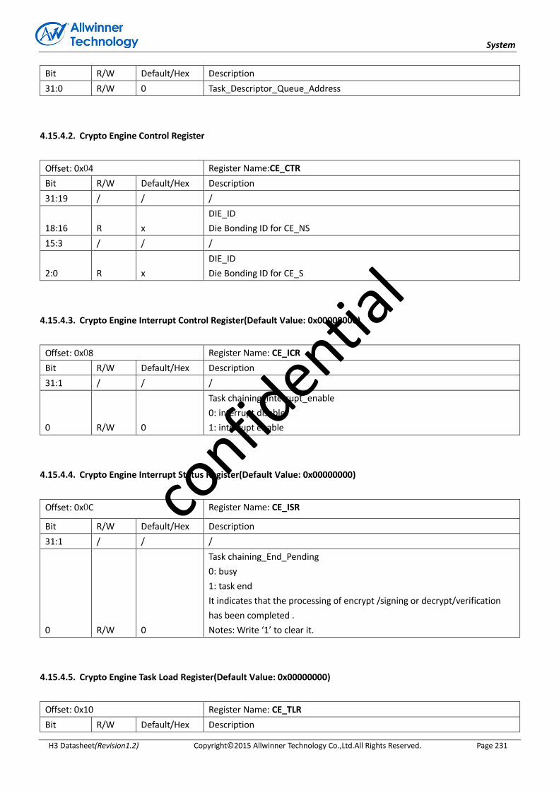
System
H3 Datasheet(Revision1.2) Copyright© 2015 Allwinner Technology Co.,Ltd.All Rights Reserved. Page 231
Bit R/W Default/Hex Description
31:0 R/W 0 Task_Descriptor_Queue_Address
4.15.4.2. Crypto Engine Control Register
Offset: 0x04 Register Name:CE_CTR
Bit R/W Default/Hex Description
31:19 / / /
18:16 R x
DIE_ID
Die Bonding ID for CE_NS
15:3 / / /
2:0 R x
DIE_ID
Die Bonding ID for CE_S
4.15.4.3. Crypto Engine Interrupt Control Register(Default Value: 0x00000000)
Offset: 0x08 Register Name: CE_ICR
Bit R/W Default/Hex Description
31:1 / / /
0 R/W 0
Task chaining_interrupt_enable
0: interrupt disable
1: interrupt enable
4.15.4.4. Crypto Engine Interrupt Status Register(Default Value: 0x00000000)
Offset: 0x0C Register Name: CE_ISR
Bit R/W Default/Hex Description
31:1 / / /
0 R/W 0
Task chaining_End_Pending
0: busy
1: task end
It indicates that the processing of encrypt /signing or decrypt/verification
has been completed .
Notes: Write ‘1’ to clear it.
4.15.4.5. Crypto Engine Task Load Register(Default Value: 0x00000000)
Offset: 0x10 Register Name: CE_TLR
Bit R/W Default/Hex Description
confid
ential
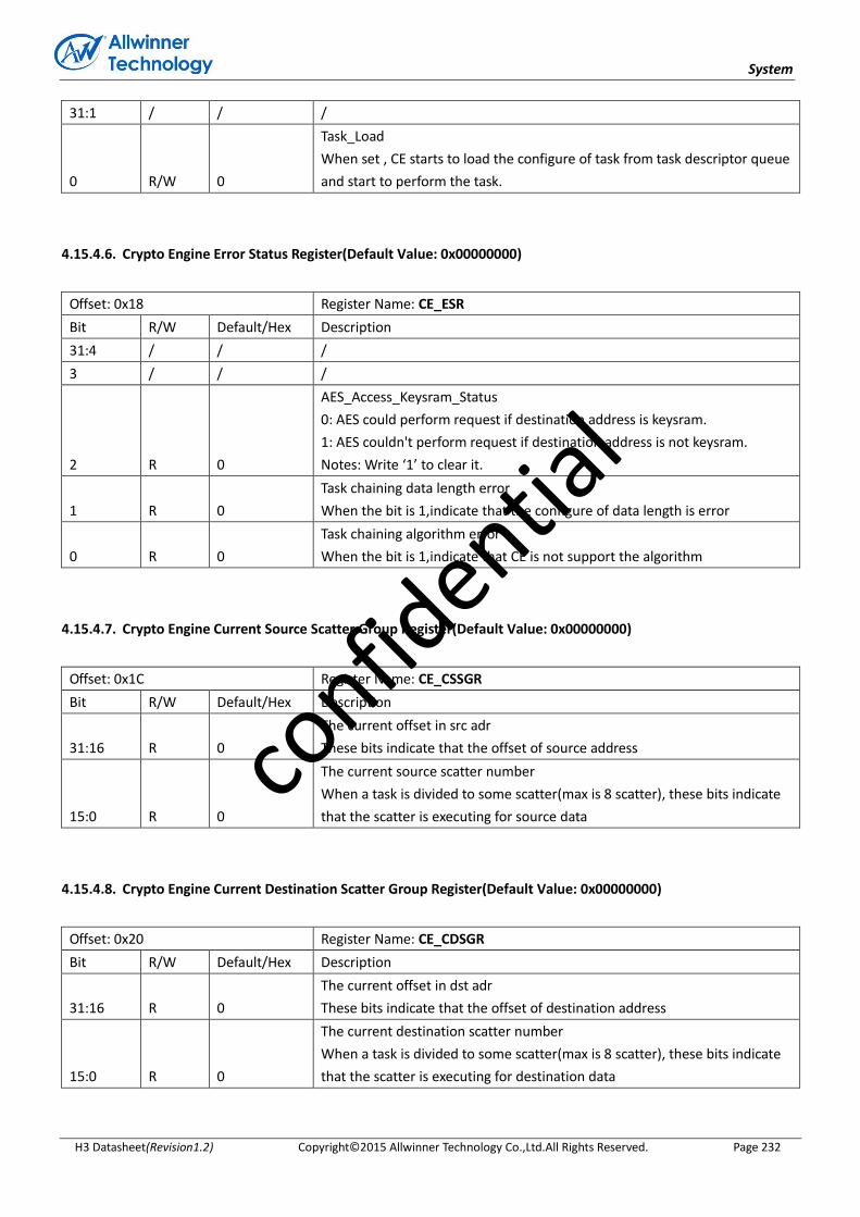
System
H3 Datasheet(Revision1.2) Copyright© 2015 Allwinner Technology Co.,Ltd.All Rights Reserved. Page 232
31:1 / / /
0 R/W 0
Task_Load
When set , CE starts to load the configure of task from task descriptor queue
and start to perform the task.
4.15.4.6. Crypto Engine Error Status Register(Default Value: 0x00000000)
Offset: 0x18 Register Name: CE_ESR
Bit R/W Default/Hex Description
31:4 / / /
3 / / /
2 R 0
AES_Access_Keysram_Status
0: AES could perform request if destination address is keysram.
1: AES couldn't perform request if destination address is not keysram.
Notes: Write ‘1’ to clear it.
1 R 0
Task chaining data length error
When the bit is 1,indicate that the configure of data length is error
0 R 0
Task chaining algorithm error
When the bit is 1,indicate that CE is not support the algorithm
4.15.4.7. Crypto Engine Current Source Scatter Group Register(Default Value: 0x00000000)
Offset: 0x1C Register Name: CE_CSSGR
Bit R/W Default/Hex Description
31:16 R 0
The current offset in src adr
These bits indicate that the offset of source address
15:0 R 0
The current source scatter number
When a task is divided to some scatter(max is 8 scatter), these bits indicate
that the scatter is executing for source data
4.15.4.8. Crypto Engine Current Destination Scatter Group Register(Default Value: 0x00000000)
Offset: 0x20 Register Name: CE_CDSGR
Bit R/W Default/Hex Description
31:16 R 0
The current offset in dst adr
These bits indicate that the offset of destination address
15:0 R 0
The current destination scatter number
When a task is divided to some scatter(max is 8 scatter), these bits indicate
that the scatter is executing for destination data
confid
ential
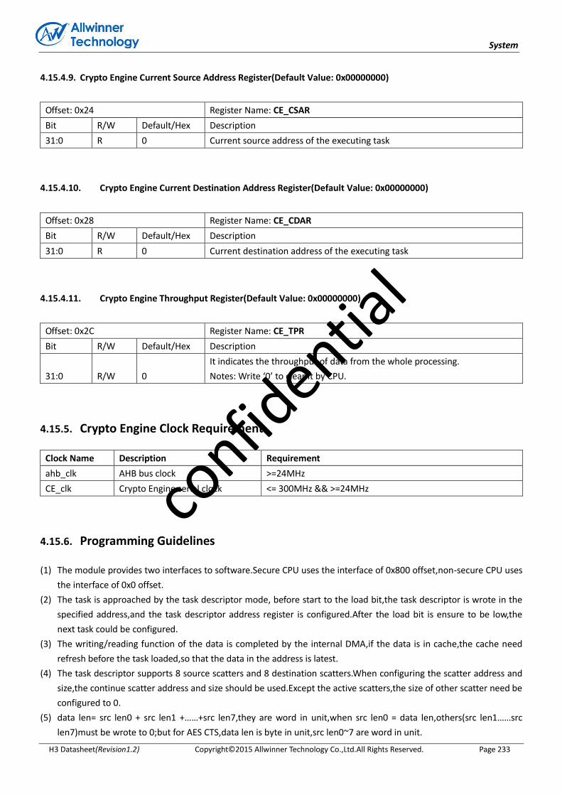
System
H3 Datasheet(Revision1.2) Copyright© 2015 Allwinner Technology Co.,Ltd.All Rights Reserved. Page 233
4.15.4.9. Crypto Engine Current Source Address Register(Default Value: 0x00000000)
Offset: 0x24 Register Name: CE_CSAR
Bit R/W Default/Hex Description
31:0 R 0 Current source address of the executing task
4.15.4.10. Crypto Engine Current Destination Address Register(Default Value: 0x00000000)
Offset: 0x28 Register Name: CE_CDAR
Bit R/W Default/Hex Description
31:0 R 0 Current destination address of the executing task
4.15.4.11. Crypto Engine Throughput Register(Default Value: 0x00000000)
Offset: 0x2C Register Name: CE_TPR
Bit R/W Default/Hex Description
31:0 R/W 0
It indicates the throughput of data from the whole processing.
Notes: Write ‘0’ to clear it by CPU.
4.15.5. Crypto Engine Clock Requirement
Clock Name Description Requirement
ahb_clk AHB bus clock >=24MHz
CE_clk Crypto Engine serial clock <= 300MHz && >=24MHz
4.15.6. Programming Guidelines
(1) The module provides two interfaces to software.Secure CPU uses the interface of 0x800 offset,non-secure CPU uses
the interface of 0x0 offset.
(2) The task is approached by the task descriptor mode, before start to the load bit,the task descriptor is wrote in the
specified address,and the task descriptor address register is configured.After the load bit is ensure to be low,the
next task could be configured.
(3) The writing/reading function of the data is completed by the internal DMA,if the data is in cache,the cache need
refresh before the task loaded,so that the data in the address is latest.
(4) The task descriptor supports 8 source scatters and 8 destination scatters.When configuring the scatter address and
size,the continue scatter address and size should be used.Except the active scatters,the size of other scatter need be
configured to 0.
(5) data len= src len0 + src len1 +……+src len7,they are word in unit,when src len0 = data len,others(src len1……src
len7)must be wrote to 0;but for AES CTS,data len is byte in unit,src len0~7 are word in unit.
confid
ential
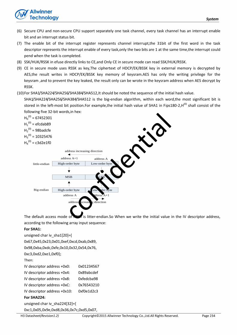
System
H3 Datasheet(Revision1.2) Copyright© 2015 Allwinner Technology Co.,Ltd.All Rights Reserved. Page 234
(6) Secure CPU and non-secure CPU support separately one task channel, every task channel has an interrupt enable
bit and an interrupt status bit.
(7) The enable bit of the interrupt register represents channel interrupt,the 31bit of the first word in the task
descriptor represents the interrupt enable of every task,only the two bits are 1 at the same time,the interrupt could
pend when the task is completed.
(8) SSK/HUK/RSSK in efuse directly links to CE,and Only CE in secure mode can read SSK/HUK/RSSK.
(9) CE in secure mode uses RSSK as key,The ciphertext of HDCP/EK/BSSK key in external memory is decrypted by
AES,the result writes in HDCP/EK/BSSK key memory of keysram.AES has only the writing privilege for the
keysram ,and to prevent the key leaked, the result only can be wrote in the keysram address when AES decrypt by
RSSK.
(10) For SHA1/SHA224/SHA256/SHA384/SHA512,It should be noted the sequence of the initial hash value.
SHA1/SHA224/SHA256/SHA384/SHA512 is the big-endian algorithm, within each word,the most significant bit is
stored in the left-most bit position.For example,the initial hash value of SHA1 in Fips180-2,H(0) shall consist of the
following five 32-bit words,in hex:
H0(0) = 67452301
H1(0) = efcdab89
H2(0) = 98badcfe
H3(0) = 10325476
H4(0) = c3d2e1f0
High-order byte Low-order byte
address A address A+1
address increasing direction
Big-endian
MSB LSB
High-order byte Low-order byte
address Aaddress A+1
address increasing direction
little-endian
The default access mode of ARM is litter-endian.So When we write the initial value in the IV descriptor address,
according to the following array input sequence:
For SHA1:
unsigned char iv_sha1[20]={
0x67,0x45,0x23,0x01,0xef,0xcd,0xab,0x89,
0x98,0xba,0xdc,0xfe,0x10,0x32,0x54,0x76,
0xc3,0xd2,0xe1,0xf0};
Then:
IV descriptor address +0x0: 0x01234567
IV descriptor address +0x4: 0x89abcdef
IV descriptor address +0x8: 0xfedcba98
IV descriptor address +0xC: 0x76543210
IV descriptor address +0x10: 0xf0e1d2c3
For SHA224:
unsigned char iv_sha224[32]={
0xc1,0x05,0x9e,0xd8,0x36,0x7c,0xd5,0x07,
confid
ential

System
H3 Datasheet(Revision1.2) Copyright© 2015 Allwinner Technology Co.,Ltd.All Rights Reserved. Page 235
0x30,0x70,0xdd,0x17,0xf7,0x0e,0x59,0x39,
0xff,0xc0,0x0b,0x31,0x68,0x58,0x15,0x11,
0x64,0xf9,0x8f,0xa7,0xbe,0xfa,0x4f,0xa4};
For SHA256:
unsigned char iv_sha256[32]={
0x6a,0x09,0xe6,0x67,0xbb,0x67,0xae,0x85,
0x3c,0x6e,0xf3,0x72,0xa5,0x4f,0xf5,0x3a,
0x51,0x0e,0x52,0x7f,0x9b,0x05,0x68,0x8c,
0x1f,0x83,0xd9,0xab,0x5b,0xe0,0xcd,0x19};
For SHA384:
unsigned char iv_sha384[64]={
0xcb,0xbb,0x9d,0x5d,0xc1,0x05,0x9e,0xd8,
0x62,0x9a,0x29,0x2a,0x36,0x7c,0xD5,0x07,
0x91,0x59,0x01,0x5a,0x30,0x70,0xdd,0x17,
0x15,0x2f,0xec,0xd8,0xf7,0x0e,0x59,0x39,
0x67,0x33,0x26,0x67,0xff,0xc0,0x0b,0x31,
0x8e,0xb4,0x4a,0x87,0x68,0x58,0x15,0x11,
0xdb,0x0c,0x2e,0x0d,0x64,0xf9,0x8f,0xa7,
0x47,0xb5,0x48,0x1d,0xbe,0xfa,0x4f,0xa4};
For SHA512:
unsigned char iv_sha512[64]={
0x6a,0x09,0xe6,0x67,0xf3,0xbc,0xc9,0x08,
0xbb,0x67,0xae,0x85,0x84,0xca,0xa7,0x3b,
0x3c,0x6e,0xf3,0x72,0xfe,0x94,0xf8,0x2b,
0xa5,0x4f,0xf5,0x3a,0x5f,0x1d,0x36,0xf1,
0x51,0x0e,0x52,0x7f,0xad,0xe6,0x82,0xd1,
0x9b,0x05,0x68,0x8c,0x2b,0x3e,0x6c,0x1f,
0x1f,0x83,0xd9,0xab,0xfb,0x41,0xbd,0x6b,
0x5b,0xe0,0xcd,0x19,0x13,0x7e,0x21,0x79}; confid
ential

System
H3 Datasheet(Revision1.2) Copyright© 2015 Allwinner Technology Co.,Ltd.All Rights Reserved. Page 236
4.16. Security ID
4.16.1. Overview
There is one 2Kbit on chip EFUSE, which provides 128-bit, 64-bit and one 32-bit electrical fuses for security application.
The users can use them as root key, security JTAG key and other applications.
It includes the following features:
128-bit electrical fuses for chip ID
64-bit electrical fuses for thermal sensor
confid
ential

System
H3 Datasheet(Revision1.2) Copyright© 2015 Allwinner Technology Co.,Ltd.All Rights Reserved. Page 237
4.17. Secure Memory Controller
4.17.1. Overview
The SMC is an Advanced Microcontroller Bus Architecture compliant System-on-Chip peripheral. It is a
high-performance, area-optimized address space controller with on-chip AMBA bus interfaces that conform to the
AMBA Advanced extensible Interface protocol and the AMBA Advanced Peripheral Bus protocol.
You can configure the SMC to provide the optimum security address region control functions required for your intended
application.
The SMC includes the following features:
Enables you to program security access permissions each address region.
Permits the transfer of data between master and slave only if the security status of the AXI transaction matches
the security settings of the memory region it addresses.
4.17.2. Functionalities Description
By default, the SMC performs read or write speculative that means it forwards an AXI transaction address to a slave,
before it verifies that the AXI transaction is permitted to read address or write address respectively.
The SMC only permits the transfer of data between its AXI bus interfaces, after verifying the access that the read or
write access is permitted respectively. If the verification fails, then it prevents the transfer of data between the master
and slave as Denied AXI transactions.
When the speculative accesses are disabled, the SMC verifies the permissions of the access before it forwards the
access to the salve. If the SMC:
Permits the access, it commences an AXI transaction to the slave, and it adds one clock latency.
Denies the access, it prevents the transfer of data between the master and slave. In this situation, the slave is
unaware when the SMC prevents the master from accessing the slave.
confid
ential

System
H3 Datasheet(Revision1.2) Copyright© 2015 Allwinner Technology Co.,Ltd.All Rights Reserved. Page 238
4.17.2.1. DRM Block Diagram
Secure ZoneDRM
Non-secure Zone
DRAM SPACE
S.M. stands for Secure Mater
G. NS.M stands for General Non-secure Master
D. NS.M stands for Non-secure Master appointed by DRM
G.NS.MNSZ
DRM
SZ
D.NS.MNSZ
DRM
SZ
S.MNSZ
DRM
SZ
G.NS.M only can read data from NSZ and write data into NSZ
D.NS.M can read data from NSZ and DRM, but only can write data into DRM
S.M can read data from the whole DRAM SPACE
Figure 4-12. DRM Block Diagram
4.17.2.2. Master ID Table
Table 4-2. Master and Master ID
ID Master ID Master
0 CPU 12 VE
1 GPU 13 CSI
2 CPUS 14 NAND
3 ATH (test interface for AHB) 15 Crypto Engine
4 USB0 16 DE_RT-MIXER0
5 MSTG0 (SD/eMMC0) 17 DE_RT-MIXER1
6 MSTG1 (SD/eMMC1) 18 DE_RT-WB
7 MSTG2 (SD/eMMC2) 19
8 USB1 20 USB3
9 USB2 21 TS
10 EMAC 22 DE Interlace
11 23
confid
ential
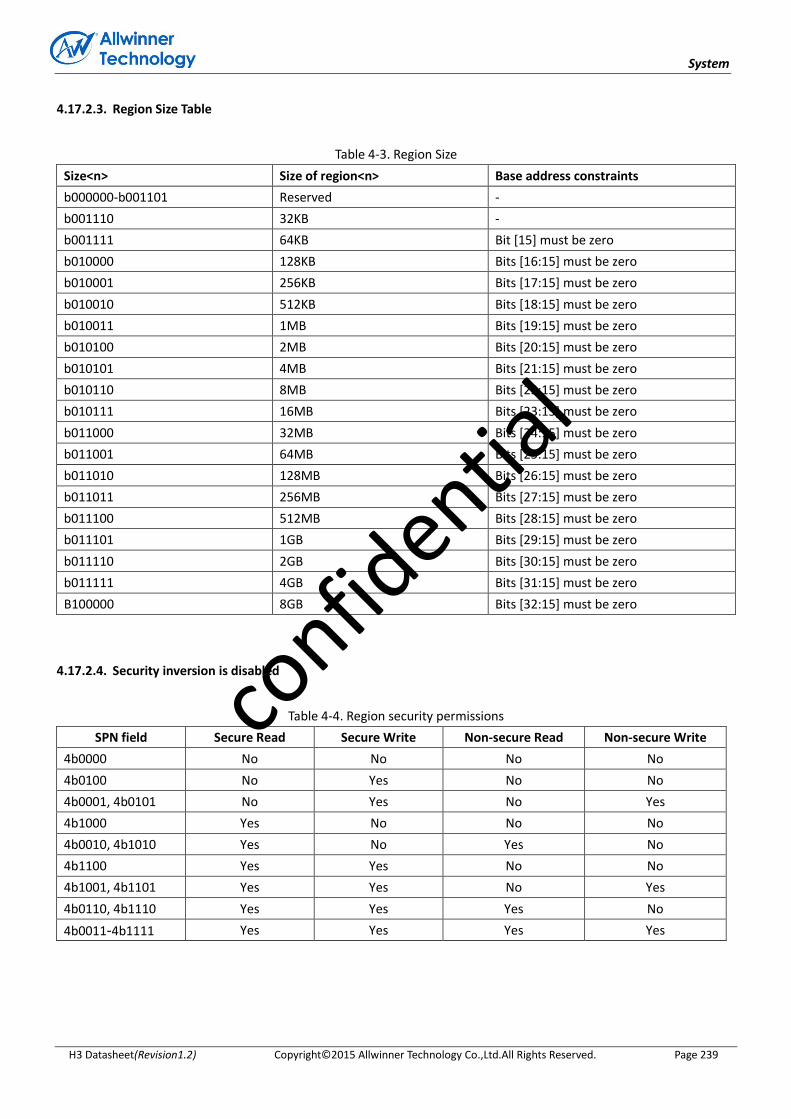
System
H3 Datasheet(Revision1.2) Copyright© 2015 Allwinner Technology Co.,Ltd.All Rights Reserved. Page 239
4.17.2.3. Region Size Table
Table 4-3. Region Size
Size<n> Size of region<n> Base address constraints
b000000-b001101 Reserved -
b001110 32KB -
b001111 64KB Bit [15] must be zero
b010000 128KB Bits [16:15] must be zero
b010001 256KB Bits [17:15] must be zero
b010010 512KB Bits [18:15] must be zero
b010011 1MB Bits [19:15] must be zero
b010100 2MB Bits [20:15] must be zero
b010101 4MB Bits [21:15] must be zero
b010110 8MB Bits [22:15] must be zero
b010111 16MB Bits [23:15] must be zero
b011000 32MB Bits [24:15] must be zero
b011001 64MB Bits [25:15] must be zero
b011010 128MB Bits [26:15] must be zero
b011011 256MB Bits [27:15] must be zero
b011100 512MB Bits [28:15] must be zero
b011101 1GB Bits [29:15] must be zero
b011110 2GB Bits [30:15] must be zero
b011111 4GB Bits [31:15] must be zero
B100000 8GB Bits [32:15] must be zero
4.17.2.4. Security inversion is disabled
Table 4-4. Region security permissions
SPN field Secure Read Secure Write Non-secure Read Non-secure Write
4b0000 No No No No
4b0100 No Yes No No
4b0001, 4b0101 No Yes No Yes
4b1000 Yes No No No
4b0010, 4b1010 Yes No Yes No
4b1100 Yes Yes No No
4b1001, 4b1101 Yes Yes No Yes
4b0110, 4b1110 Yes Yes Yes No
4b0011-4b1111 Yes Yes Yes Yes
confid
ential

System
H3 Datasheet(Revision1.2) Copyright© 2015 Allwinner Technology Co.,Ltd.All Rights Reserved. Page 240
4.17.2.5. Security inversion is enabled
If you enable security inversion, the SMC permits you to program any combination of security permissions as Table 4-5
shows.
Table 4-5. Region security permissions
SPN field Secure Read Secure Write Non-secure Read Non-secure Write
4b0000 No No No No
4b0001 No No No Yes
4b0010 No No Yes No
4b0011 No No Yes Yes
4b0100 No Yes No No
4b0101 No Yes No Yes
4b0110 No Yes Yes No
4b0111 No Yes Yes Yes
4b1000 Yes No No No
4b1001 Yes No No Yes
4b1010 Yes No Yes No
4b1011 Yes No Yes Yes
4b1100 Yes Yes No No
4b1101 Yes Yes No Yes
4b1110 Yes Yes Yes No
4b1111 Yes Yes Yes Yes
4.17.3. SMC Register List
Module Name Base Address
SMC 0x01C1E000
Register Name Offset Description
SMC_CONFIG_REG 0x0 SMC Configuration Register
SMC_ACTION_REG 0x4 SMC Action Register
SMC_LD_RANGE_REG 0x8 SMC Lock Down Range Register
SMC_LD_SELECT_REG 0xC SMC Lock Down Select Register
SMC_INT_STATUS_REG 0x10 SMC Interrupt Status Register
SMC_INT_CLEAR_REG 0x14 SMC Interrupt Clear Register
SMC_MST_BYP_REG 0x18 SMC Master Bypass Register
SMC_MST_SEC_REG 0x1C SMC Master Secure Register
SMC_FAIL_ADDR_REG 0x20 SMC Fail Address Register
SMC_FAIL_CTRL_REG 0x28 SMC Fail Control Register
SMC_FAIL_ID_REG 0x2C SMC Fail ID Register
SMC_SPECU_CTRL_REG 0x30 SMC Speculation Control Register
SMC_SEC_INV_EN_REG 0x34 SMC Security Inversion Enable Register
confid
ential
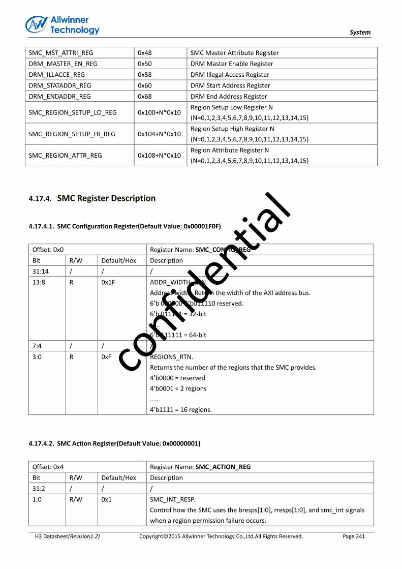
System
H3 Datasheet(Revision1.2) Copyright© 2015 Allwinner Technology Co.,Ltd.All Rights Reserved. Page 241
SMC_MST_ATTRI_REG 0x48 SMC Master Attribute Register
DRM_MASTER_EN_REG 0x50 DRM Master Enable Register
DRM_ILLACCE_REG 0x58 DRM Illegal Access Register
DRM_STATADDR_REG 0x60 DRM Start Address Register
DRM_ENDADDR_REG 0x68 DRM End Address Register
SMC_REGION_SETUP_LO_REG 0x100+N*0x10 Region Setup Low Register N
(N=0,1,2,3,4,5,6,7,8,9,10,11,12,13,14,15)
SMC_REGION_SETUP_HI_REG 0x104+N*0x10 Region Setup High Register N
(N=0,1,2,3,4,5,6,7,8,9,10,11,12,13,14,15)
SMC_REGION_ATTR_REG 0x108+N*0x10 Region Attribute Register N
(N=0,1,2,3,4,5,6,7,8,9,10,11,12,13,14,15)
4.17.4. SMC Register Description
4.17.4.1. SMC Configuration Register(Default Value: 0x00001F0F)
Offset: 0x0 Register Name: SMC_CONFIG_REG
Bit R/W Default/Hex Description
31:14 / / /
13:8 R 0x1F ADDR_WIDTH_RTN.
Address width. Return the width of the AXI address bus.
6’b 000000-6’b011110 reserved.
6’b 011111 = 32-bit
……
6’b 111111 = 64-bit
7:4 / / /
3:0 R 0xF REGIONS_RTN.
Returns the number of the regions that the SMC provides.
4’b0000 = reserved
4’b0001 = 2 regions
……
4’b1111 = 16 regions.
4.17.4.2. SMC Action Register(Default Value: 0x00000001)
Offset: 0x4 Register Name: SMC_ACTION_REG
Bit R/W Default/Hex Description
31:2 / / /
1:0 R/W 0x1 SMC_INT_RESP.
Control how the SMC uses the bresps[1:0], rresps[1:0], and smc_int signals
when a region permission failure occurs:
confid
ential
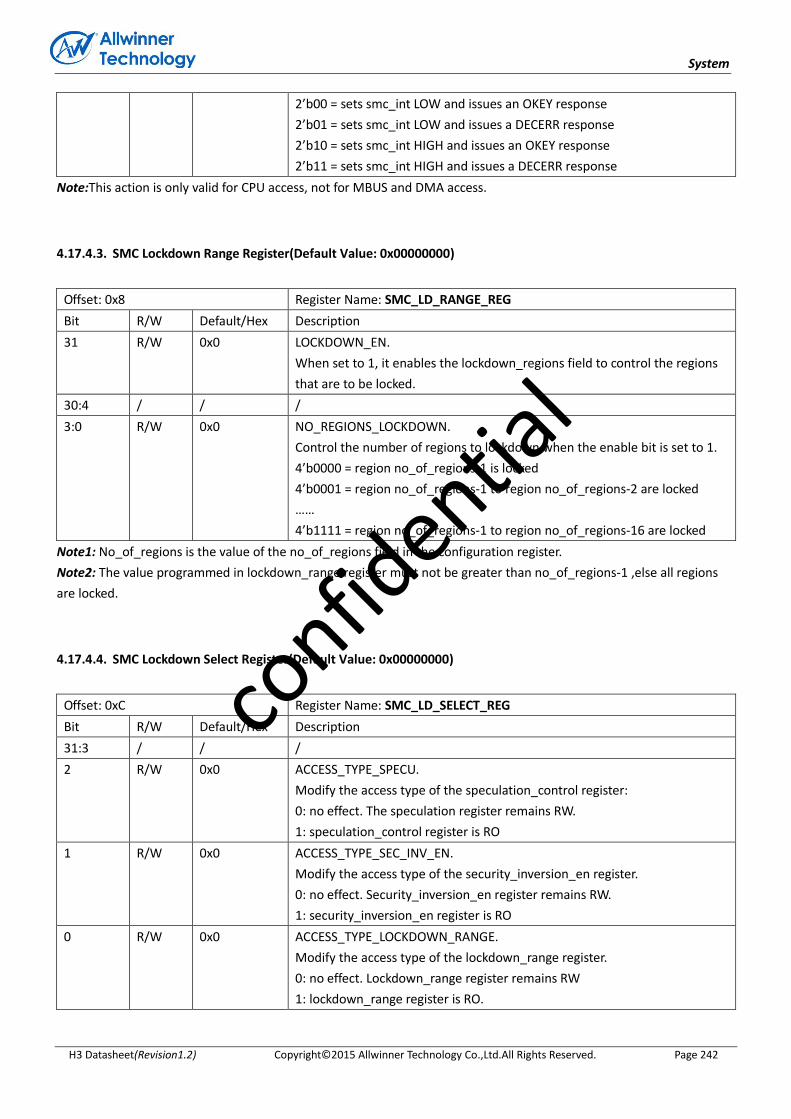
System
H3 Datasheet(Revision1.2) Copyright© 2015 Allwinner Technology Co.,Ltd.All Rights Reserved. Page 242
2’b00 = sets smc_int LOW and issues an OKEY response
2’b01 = sets smc_int LOW and issues a DECERR response
2’b10 = sets smc_int HIGH and issues an OKEY response
2’b11 = sets smc_int HIGH and issues a DECERR response
Note:This action is only valid for CPU access, not for MBUS and DMA access.
4.17.4.3. SMC Lockdown Range Register(Default Value: 0x00000000)
Offset: 0x8 Register Name: SMC_LD_RANGE_REG
Bit R/W Default/Hex Description
31 R/W 0x0 LOCKDOWN_EN.
When set to 1, it enables the lockdown_regions field to control the regions
that are to be locked.
30:4 / / /
3:0 R/W 0x0 NO_REGIONS_LOCKDOWN.
Control the number of regions to lockdown when the enable bit is set to 1.
4’b0000 = region no_of_regions-1 is locked
4’b0001 = region no_of_regions-1 to region no_of_regions-2 are locked
……
4’b1111 = region no_of_regions-1 to region no_of_regions-16 are locked
Note1: No_of_regions is the value of the no_of_regions field in the configuration register.
Note2: The value programmed in lockdown_range register must not be greater than no_of_regions-1 ,else all regions
are locked.
4.17.4.4. SMC Lockdown Select Register(Default Value: 0x00000000)
Offset: 0xC Register Name: SMC_LD_SELECT_REG
Bit R/W Default/Hex Description
31:3 / / /
2 R/W 0x0 ACCESS_TYPE_SPECU.
Modify the access type of the speculation_control register:
0: no effect. The speculation register remains RW.
1: speculation_control register is RO
1 R/W 0x0 ACCESS_TYPE_SEC_INV_EN.
Modify the access type of the security_inversion_en register.
0: no effect. Security_inversion_en register remains RW.
1: security_inversion_en register is RO
0 R/W 0x0 ACCESS_TYPE_LOCKDOWN_RANGE.
Modify the access type of the lockdown_range register.
0: no effect. Lockdown_range register remains RW
1: lockdown_range register is RO.
confid
ential

System
H3 Datasheet(Revision1.2) Copyright© 2015 Allwinner Technology Co.,Ltd.All Rights Reserved. Page 243
4.17.4.5. SMC Interrupt Status Register(Default Value: 0x00000000)
Offset: 0x10 Register Name: SMC_INT_STATUS_REG
Bit R/W Default/Hex Description
31:2 / / /
1 R 0x0 INT_OVERRUN.
When set to 1, it indicates the occurrence of two or more region permission
failure since the interrupt was last cleared.
0 R 0x0 INT_STATUS.
Return the status of the interrupt.
0: interrupt is inactive.
1: interrupt is active.
4.17.4.6. SMC Interrupt Clear Register(Default Value: 0x00000000)
Offset: 0x14 Register Name: SMC_INT_CLEAR_REG
Bit R/W Default/Hex Description
31:0 R/W 0x0 SMC_CLR_REG.
Write any value to the int_clear register sets the :
Status bit to 0 in the int_status register
Overrun bit to 0 in the int_status register.
Note: It will be auto cleared after the write operation.
4.17.4.7. SMC Master Bypass Register(Default Value: 0xFFFFFFFF)
Offset: 0x18 Register Name: SMC_MST_BYP_REG
Bit R/W Default/Hex Description
31:0 R/W 0xFFFFFFFF SMC_MASTER_BYPASS_EN.
SMC Master n Bypass Enable.
(n = 0~31, see the Table 4-2. MASTER and MASTER ID for detail.)
Note: Bit[31:0] stand for Master ID [31:0]
If the master n bypass enable is set to 0, the master n access must be
through the SMC.
0: Bypass Disable
1: Bypass Enable.
4.17.4.8. SMC Master Secure Register(Default Value: 0x00000000)
Offset: 0x1C Register Name: SMC_MST_SEC_REG
Bit R/W Default/Hex Description
confid
ential
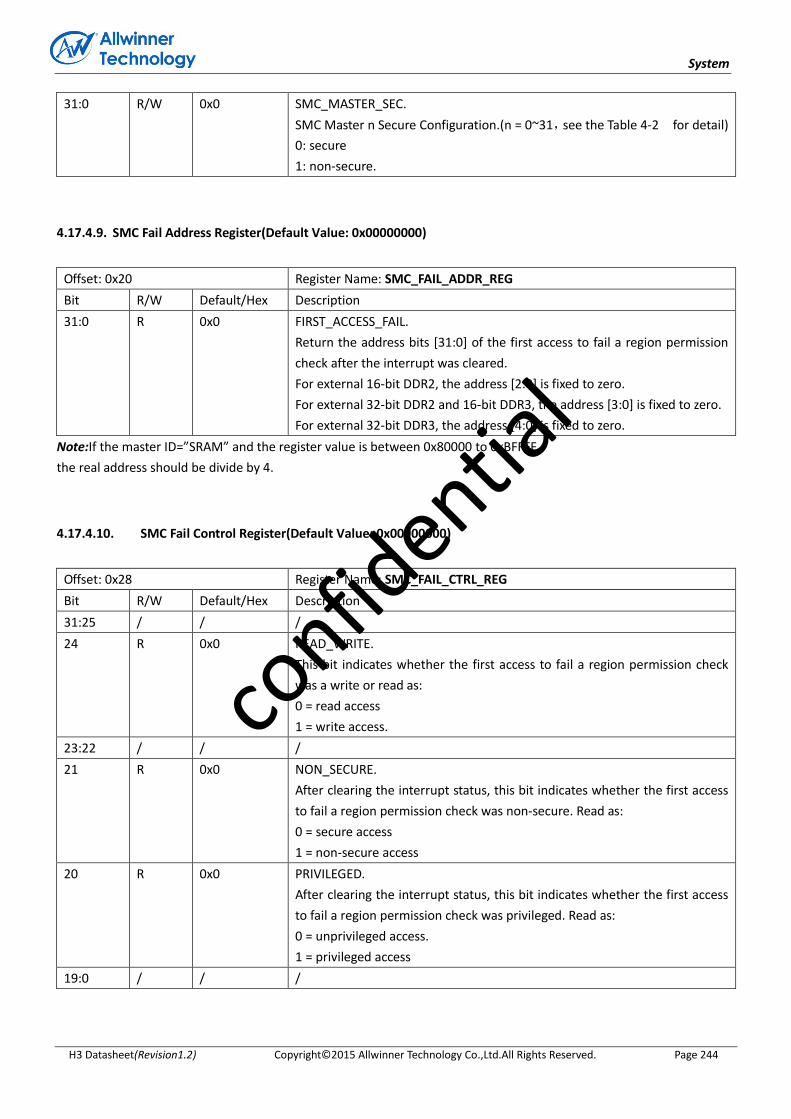
System
H3 Datasheet(Revision1.2) Copyright© 2015 Allwinner Technology Co.,Ltd.All Rights Reserved. Page 244
31:0 R/W 0x0 SMC_MASTER_SEC.
SMC Master n Secure Configuration.(n = 0~31,see the Table 4-2 for detail)
0: secure
1: non-secure.
4.17.4.9. SMC Fail Address Register(Default Value: 0x00000000)
Offset: 0x20 Register Name: SMC_FAIL_ADDR_REG
Bit R/W Default/Hex Description
31:0 R 0x0 FIRST_ACCESS_FAIL.
Return the address bits [31:0] of the first access to fail a region permission
check after the interrupt was cleared.
For external 16-bit DDR2, the address [2:0] is fixed to zero.
For external 32-bit DDR2 and 16-bit DDR3, the address [3:0] is fixed to zero.
For external 32-bit DDR3, the address [4:0] is fixed to zero.
Note:If the master ID=”SRAM” and the register value is between 0x80000 to 0xBFFFF,
the real address should be divide by 4.
4.17.4.10. SMC Fail Control Register(Default Value: 0x00000000)
Offset: 0x28 Register Name: SMC_FAIL_CTRL_REG
Bit R/W Default/Hex Description
31:25 / / /
24 R 0x0 READ_WRITE.
This bit indicates whether the first access to fail a region permission check
was a write or read as:
0 = read access
1 = write access.
23:22 / / /
21 R 0x0 NON_SECURE.
After clearing the interrupt status, this bit indicates whether the first access
to fail a region permission check was non-secure. Read as:
0 = secure access
1 = non-secure access
20 R 0x0 PRIVILEGED.
After clearing the interrupt status, this bit indicates whether the first access
to fail a region permission check was privileged. Read as:
0 = unprivileged access.
1 = privileged access
19:0 / / /
confid
ential

System
H3 Datasheet(Revision1.2) Copyright© 2015 Allwinner Technology Co.,Ltd.All Rights Reserved. Page 245
4.17.4.11. SMC Fail ID Register(Default Value: 0x00001F00)
Offset: 0x2C Register Name: SMC_FAIL_ID_REG
Bit R/W Default/Hex Description
31:24 / / /
23:16 R 0x0 FAIL_BST_LEN.
Fail burst length.
0 = 1 word length
……
0xf =16 words length
15:8 / / /
7:0 R 0x0 FAIL_MASTER_ID.
Fail Master ID.
The value stands for master id, see the Table 4-2 MASTER and MASTER ID for
detail.
4.17.4.12. SMC Speculation Control Register(Default Value: 0x00000000)
Offset: 0x30 Register Name: SMC_SPECU_CTRL_REG
Bit R/W Default/Hex Description
31:2 / / /
1 R/W 0x0 WRITE_SPECU.
Write_speculation. Control the write access speculation:
0 = write access speculation is enabled
1 = write access speculation is disabled.
0 R/W 0x0 READ_SPECU.
Read_speculation. Control the read access speculation:
0 = read access speculation is enabled
1 = read access speculation is disabled.
4.17.4.13. SMC Security Inversion Enable Register(Default Value: 0x00000000)
Offset: 0x34 Register Name: SMC_SEC_INV_EN_REG
Bit R/W Default/Hex Description
31:1 / / /
0 R/W 0x0 SEC_INV_EN.
Security_inversion_en. Controls whether the SMC permits security inversion
to occur.
0 = security inversion is not permitted.
1 = security inversion is permitted. This enables a region to be accessible to
masters in Non-secure state but not accessible to masters in Secure state.
See Table 4-4 and Table 4-5.
confid
ential
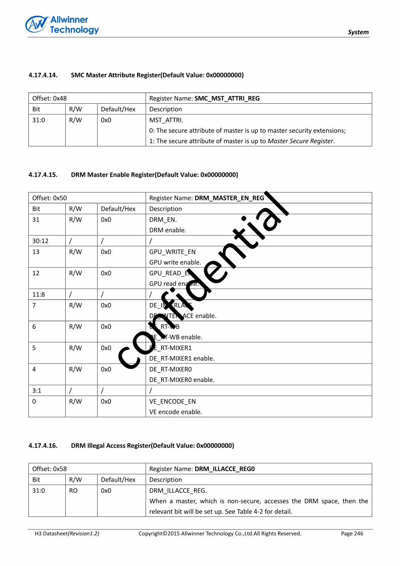
System
H3 Datasheet(Revision1.2) Copyright© 2015 Allwinner Technology Co.,Ltd.All Rights Reserved. Page 246
4.17.4.14. SMC Master Attribute Register(Default Value: 0x00000000)
Offset: 0x48 Register Name: SMC_MST_ATTRI_REG
Bit R/W Default/Hex Description
31:0 R/W 0x0 MST_ATTRI.
0: The secure attribute of master is up to master security extensions;
1: The secure attribute of master is up to Master Secure Register.
4.17.4.15. DRM Master Enable Register(Default Value: 0x00000000)
Offset: 0x50 Register Name: DRM_MASTER_EN_REG
Bit R/W Default/Hex Description
31 R/W 0x0 DRM_EN.
DRM enable.
30:12 / / /
13 R/W 0x0 GPU_WRITE_EN
GPU write enable.
12 R/W 0x0 GPU_READ_EN
GPU read enable.
11:8 / / /
7 R/W 0x0 DE_INTERLACE
DE_ INTERLACE enable.
6 R/W 0x0 DE_RT-WB
DE_RT-WB enable.
5 R/W 0x0 DE_RT-MIXER1
DE_RT-MIXER1 enable.
4 R/W 0x0 DE_RT-MIXER0
DE_RT-MIXER0 enable.
3:1 / / /
0 R/W 0x0 VE_ENCODE_EN
VE encode enable.
4.17.4.16. DRM Illegal Access Register(Default Value: 0x00000000)
Offset: 0x58 Register Name: DRM_ILLACCE_REG0
Bit R/W Default/Hex Description
31:0 RO 0x0 DRM_ILLACCE_REG.
When a master, which is non-secure, accesses the DRM space, then the
relevant bit will be set up. See Table 4-2 for detail.
confid
ential
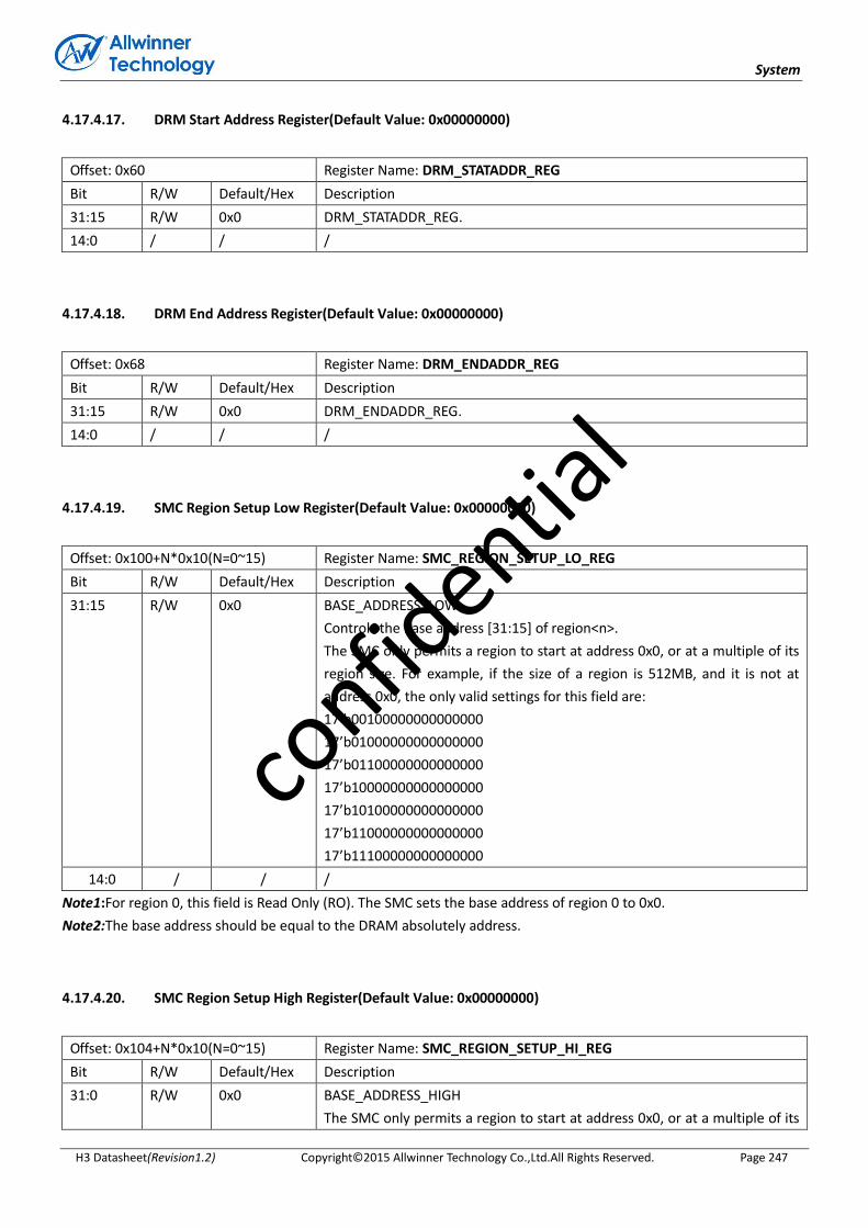
System
H3 Datasheet(Revision1.2) Copyright© 2015 Allwinner Technology Co.,Ltd.All Rights Reserved. Page 247
4.17.4.17. DRM Start Address Register(Default Value: 0x00000000)
Offset: 0x60 Register Name: DRM_STATADDR_REG
Bit R/W Default/Hex Description
31:15 R/W 0x0 DRM_STATADDR_REG.
14:0 / / /
4.17.4.18. DRM End Address Register(Default Value: 0x00000000)
Offset: 0x68 Register Name: DRM_ENDADDR_REG
Bit R/W Default/Hex Description
31:15 R/W 0x0 DRM_ENDADDR_REG.
14:0 / / /
4.17.4.19. SMC Region Setup Low Register(Default Value: 0x00000000)
Offset: 0x100+N*0x10(N=0~15) Register Name: SMC_REGION_SETUP_LO_REG
Bit R/W Default/Hex Description
31:15 R/W 0x0 BASE_ADDRESS_LOW.
Controls the base address [31:15] of region<n>.
The SMC only permits a region to start at address 0x0, or at a multiple of its
region size. For example, if the size of a region is 512MB, and it is not at
address 0x0, the only valid settings for this field are:
17’b00100000000000000
17’b01000000000000000
17’b01100000000000000
17’b10000000000000000
17’b10100000000000000
17’b11000000000000000
17’b11100000000000000
14:0 / / /
Note1:For region 0, this field is Read Only (RO). The SMC sets the base address of region 0 to 0x0.
Note2:The base address should be equal to the DRAM absolutely address.
4.17.4.20. SMC Region Setup High Register(Default Value: 0x00000000)
Offset: 0x104+N*0x10(N=0~15) Register Name: SMC_REGION_SETUP_HI_REG
Bit R/W Default/Hex Description
31:0 R/W 0x0 BASE_ADDRESS_HIGH
The SMC only permits a region to start at address 0x0, or at a multiple of its
confid
ential

System
H3 Datasheet(Revision1.2) Copyright© 2015 Allwinner Technology Co.,Ltd.All Rights Reserved. Page 248
region size. If you program a region size to be 8GB or more, then the SMC
might ignore certain bits depending on the region size.
4.17.4.21. SMC Region Attributes Register(Default Value: 0x00000000)
Offset: 0x108+N*0x10(N=0~15) Register Name: SMC_REGION_ATTR_REG
Bit R/W Default/Hex Description
31:28 R/W 0x0 REGION_ATTR_SPN.
SP<n>. Permission setting for region <n>. if an AXI transaction occurs to
region n, the value in the sp<n> field controls whether the SMC permits the
transaction to proceed. . See Table 4-4 and Table 4-5.
27:16 / / /.
15:8 R/W 0x0 SUB_REGION_DISABLE.
Subregion_disable. Regions are split into eight equal-sized sub-regions, and
each bit enables the corresponding subregion to be disabled.
Bit [15] = 1 subregion 7 is disabled.
Bit [14] = 1 subregion 6 is disabled.
Bit [13] = 1 subregion 5 is disabled.
Bit [12] = 1 subregion 4 is disabled.
Bit [11] = 1 subregion 3 is disabled.
Bit [10] = 1 subregion 2 is disabled.
Bit [9] = 1 subregion 1 is disabled.
Bit [8] = 1 subregion 0 is disabled.
7 / / /
6:1 R/W 0x0 REGION_ATTR_SIZE.
Size<n>. Size of region<n>, see Table 3 for detail.
0 R/W 0x0 REGION_ATTR_EN.
EN<n>. Enable for region<n>.
0 = region < n> is disabled.
1 = region < n> is enabled.
Note:For region 0,this field is reserved except SPN field.
confid
ential
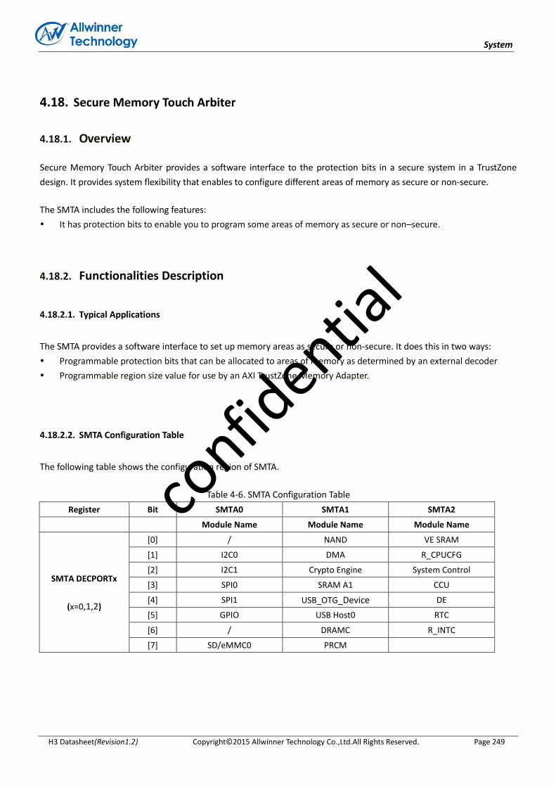
System
H3 Datasheet(Revision1.2) Copyright© 2015 Allwinner Technology Co.,Ltd.All Rights Reserved. Page 249
4.18. Secure Memory Touch Arbiter
4.18.1. Overview
Secure Memory Touch Arbiter provides a software interface to the protection bits in a secure system in a TrustZone
design. It provides system flexibility that enables to configure different areas of memory as secure or non-secure.
The SMTA includes the following features:
It has protection bits to enable you to program some areas of memory as secure or non–secure.
4.18.2. Functionalities Description
4.18.2.1. Typical Applications
The SMTA provides a software interface to set up memory areas as secure or non-secure. It does this in two ways:
Programmable protection bits that can be allocated to areas of memory as determined by an external decoder
Programmable region size value for use by an AXI TrustZone Memory Adapter.
4.18.2.2. SMTA Configuration Table
The following table shows the configuration region of SMTA.
Table 4-6. SMTA Configuration Table
Register Bit SMTA0 SMTA1 SMTA2
Module Name Module Name Module Name
SMTA DECPORTx
(x=0,1,2)
[0] / NAND VE SRAM
[1] I2C0 DMA R_CPUCFG
[2] I2C1 Crypto Engine System Control
[3] SPI0 SRAM A1 CCU
[4] SPI1 USB_OTG_Device DE
[5] GPIO USB Host0 RTC
[6] / DRAMC R_INTC
[7] SD/eMMC0 PRCM
confid
ential

System
H3 Datasheet(Revision1.2) Copyright© 2015 Allwinner Technology Co.,Ltd.All Rights Reserved. Page 250
4.18.3. SMTA Register List
Module Name Base Address
SMTA 0x01C23400
Register Name Offset Description
SMTA_DECPORT0_STA_REG 0x4 SMTA Decode Port0 Status Register
SMTA_DECPORT0_SET_REG 0x8 SMTA Decode Port0 Set Register
SMTA_DECPORT0_CLR_REG 0xC SMTA Decode Port0 Clear Register
SMTA_DECPORT1_STA_REG 0x10 SMTA Decode Port1 Status Register
SMTA_DECPORT1_SET_REG 0x14 SMTA Decode Port1 Set Register
SMTA_DECPORT1_CLR_REG 0x18 SMTA Decode Port1 Clear Register
SMTA_DECPORT2_STA_REG 0x1C SMTA Decode Port2 Status Register
SMTA_DECPORT2_SET_REG 0x20 SMTA Decode Port2 Set Register
SMTA_DECPORT2_CLR_REG 0x24 SMTA Decode Port2 Clear Register
4.18.4. SMTA Register Description
4.18.4.1. SMTA DECPORT0 Status Register(Default Value: 0x00000000)
Offset: 0x4 Register Name: SMTA_DECPORT0_STA_REG
Bit R/W Default/Hex Description
31:8 / / /
7:0 RO 0x0 STA_DEC_PROT0_OUT.
Show the status of the decode protection output:
0: = Decode region corresponding to the bit is secure
1: = Decode region corresponding to the bit is non-secure.
There is one bit of the register for each protection output (See the SMTA
Configuration Table4-6 in detail).
4.18.4.2. SMTA DECPORT0 Set Register(Default Value: 0x00000000)
Offset: 0x8 Register Name: SMTA_DECPORT0_SET_REG
Bit R/W Default/Hex Description
31:8 / / /.
7:0 WO 0x0 SET_DEC_PORT0_OUT.
Sets the corresponding decode protection output:
0: = No effect
1: = Set decode region to non-secure.
There is one bit of the register for each protection output (See the SMTA
confid
ential
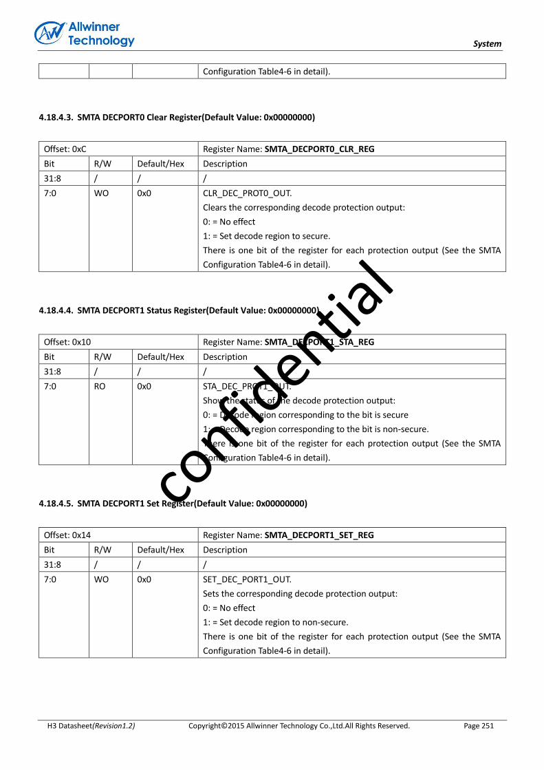
System
H3 Datasheet(Revision1.2) Copyright© 2015 Allwinner Technology Co.,Ltd.All Rights Reserved. Page 251
Configuration Table4-6 in detail).
4.18.4.3. SMTA DECPORT0 Clear Register(Default Value: 0x00000000)
Offset: 0xC Register Name: SMTA_DECPORT0_CLR_REG
Bit R/W Default/Hex Description
31:8 / / /
7:0 WO 0x0 CLR_DEC_PROT0_OUT.
Clears the corresponding decode protection output:
0: = No effect
1: = Set decode region to secure.
There is one bit of the register for each protection output (See the SMTA
Configuration Table4-6 in detail).
4.18.4.4. SMTA DECPORT1 Status Register(Default Value: 0x00000000)
Offset: 0x10 Register Name: SMTA_DECPORT1_STA_REG
Bit R/W Default/Hex Description
31:8 / / /
7:0 RO 0x0 STA_DEC_PROT1_OUT.
Show the status of the decode protection output:
0: = Decode region corresponding to the bit is secure
1: = Decode region corresponding to the bit is non-secure.
There is one bit of the register for each protection output (See the SMTA
Configuration Table4-6 in detail).
4.18.4.5. SMTA DECPORT1 Set Register(Default Value: 0x00000000)
Offset: 0x14 Register Name: SMTA_DECPORT1_SET_REG
Bit R/W Default/Hex Description
31:8 / / /
7:0 WO 0x0 SET_DEC_PORT1_OUT.
Sets the corresponding decode protection output:
0: = No effect
1: = Set decode region to non-secure.
There is one bit of the register for each protection output (See the SMTA
Configuration Table4-6 in detail).
confid
ential
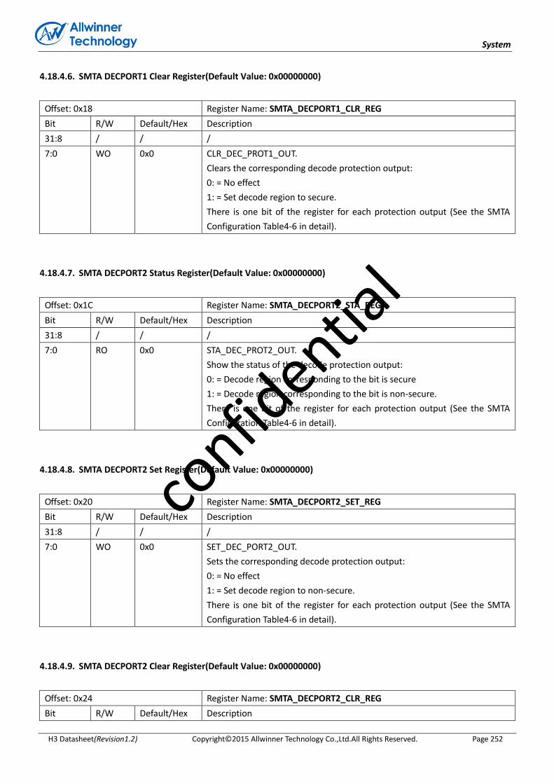
System
H3 Datasheet(Revision1.2) Copyright© 2015 Allwinner Technology Co.,Ltd.All Rights Reserved. Page 252
4.18.4.6. SMTA DECPORT1 Clear Register(Default Value: 0x00000000)
Offset: 0x18 Register Name: SMTA_DECPORT1_CLR_REG
Bit R/W Default/Hex Description
31:8 / / /
7:0 WO 0x0 CLR_DEC_PROT1_OUT.
Clears the corresponding decode protection output:
0: = No effect
1: = Set decode region to secure.
There is one bit of the register for each protection output (See the SMTA
Configuration Table4-6 in detail).
4.18.4.7. SMTA DECPORT2 Status Register(Default Value: 0x00000000)
Offset: 0x1C Register Name: SMTA_DECPORT2_STA_REG
Bit R/W Default/Hex Description
31:8 / / /
7:0 RO 0x0 STA_DEC_PROT2_OUT.
Show the status of the decode protection output:
0: = Decode region corresponding to the bit is secure
1: = Decode region corresponding to the bit is non-secure.
There is one bit of the register for each protection output (See the SMTA
Configuration Table4-6 in detail).
4.18.4.8. SMTA DECPORT2 Set Register(Default Value: 0x00000000)
Offset: 0x20 Register Name: SMTA_DECPORT2_SET_REG
Bit R/W Default/Hex Description
31:8 / / /
7:0 WO 0x0 SET_DEC_PORT2_OUT.
Sets the corresponding decode protection output:
0: = No effect
1: = Set decode region to non-secure.
There is one bit of the register for each protection output (See the SMTA
Configuration Table4-6 in detail).
4.18.4.9. SMTA DECPORT2 Clear Register(Default Value: 0x00000000)
Offset: 0x24 Register Name: SMTA_DECPORT2_CLR_REG
Bit R/W Default/Hex Description
confid
ential

System
H3 Datasheet(Revision1.2) Copyright© 2015 Allwinner Technology Co.,Ltd.All Rights Reserved. Page 253
31:8 / / /
7:0 WO 0x0 CLR_DEC_PROT2_OUT.
Clears the corresponding decode protection output:
0: = No effect
1: = Set decode region to secure.
There is one bit of the register for each protection output (See the SMTA
Configuration Table4-6 in detail).
confid
ential

System
H3 Datasheet(Revision1.2) Copyright© 2015 Allwinner Technology Co.,Ltd.All Rights Reserved. Page 254
4.19. Thermal Sensor Controller
4.19.1. Overview
The thermal sensors have become common elements in wide range of modern system on chip (SOC) platform. Thermal
sensors are used to constantly monitor the temperature on the chip.
H3 embeds one thermal sensor located in the CPU .The thermal sensor Generates interrupt to SW to lower temperature
via DVFS, on reaching a certain thermal threshold.
The Thermal Sensor Controller includes the following features:
Supports APB 32-bits bus width
Power supply voltage:3.0V
Low power dissipation
Periodic temperature measurement
Averaging filter for thermal sensor reading
Support over-temperature protection interrupt and over-temperature alarm interrupt
4.19.2. Clock and Timing Requirements
CLK_IN = 24MHz/M, M can be set in the CCU
Conversion Time = 1/(24MHz/M/14Cycles) =0.583 * M (us)
THERMAL_PER (configured by the value of THERMAL_PER) is must be greater than (ACQ1 + ACQ0+Conversion Time)
THERMAL_PER > ACQ1 + ACQ0+Conversion Time
Figure 4-13. Thermal Conversion phase
4.19.3. Thermal Sensor Register List
Module Name Base Address
confid
ential
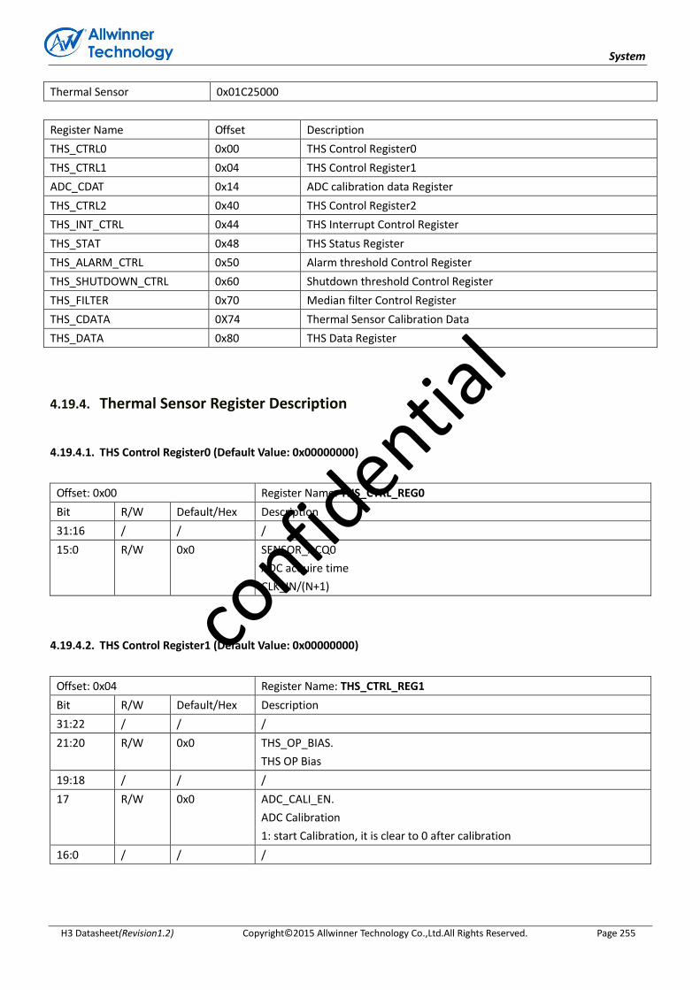
System
H3 Datasheet(Revision1.2) Copyright© 2015 Allwinner Technology Co.,Ltd.All Rights Reserved. Page 255
Thermal Sensor 0x01C25000
Register Name Offset Description
THS_CTRL0 0x00 THS Control Register0
THS_CTRL1 0x04 THS Control Register1
ADC_CDAT 0x14 ADC calibration data Register
THS_CTRL2 0x40 THS Control Register2
THS_INT_CTRL 0x44 THS Interrupt Control Register
THS_STAT 0x48 THS Status Register
THS_ALARM_CTRL 0x50 Alarm threshold Control Register
THS_SHUTDOWN_CTRL 0x60 Shutdown threshold Control Register
THS_FILTER 0x70 Median filter Control Register
THS_CDATA 0X74 Thermal Sensor Calibration Data
THS_DATA 0x80 THS Data Register
4.19.4. Thermal Sensor Register Description
4.19.4.1. THS Control Register0 (Default Value: 0x00000000)
Offset: 0x00 Register Name: THS_CTRL_REG0
Bit R/W Default/Hex Description
31:16 / / /
15:0 R/W 0x0 SENSOR_ACQ0
ADC acquire time
CLK_IN/(N+1)
4.19.4.2. THS Control Register1 (Default Value: 0x00000000)
Offset: 0x04 Register Name: THS_CTRL_REG1
Bit R/W Default/Hex Description
31:22 / / /
21:20 R/W 0x0 THS_OP_BIAS.
THS OP Bias
19:18 / / /
17 R/W 0x0 ADC_CALI_EN.
ADC Calibration
1: start Calibration, it is clear to 0 after calibration
16:0 / / /
confid
ential
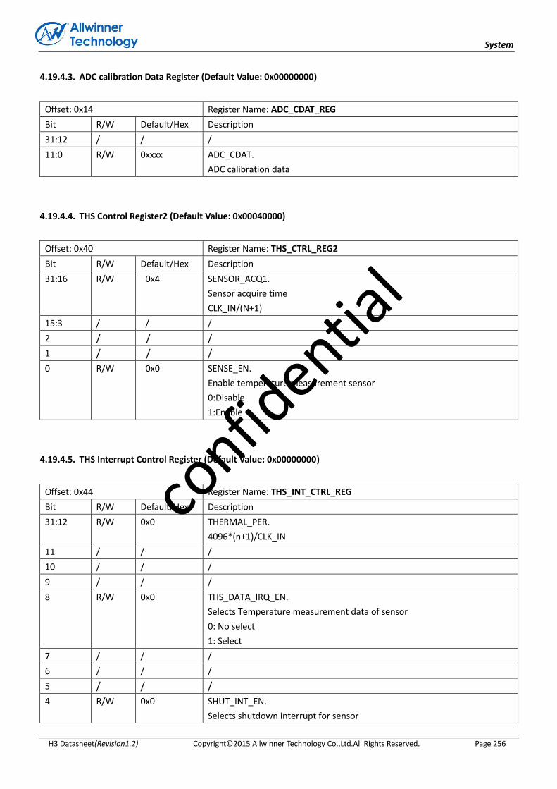
System
H3 Datasheet(Revision1.2) Copyright© 2015 Allwinner Technology Co.,Ltd.All Rights Reserved. Page 256
4.19.4.3. ADC calibration Data Register (Default Value: 0x00000000)
Offset: 0x14 Register Name: ADC_CDAT_REG
Bit R/W Default/Hex Description
31:12 / / /
11:0 R/W 0xxxx ADC_CDAT.
ADC calibration data
4.19.4.4. THS Control Register2 (Default Value: 0x00040000)
Offset: 0x40 Register Name: THS_CTRL_REG2
Bit R/W Default/Hex Description
31:16 R/W 0x4 SENSOR_ACQ1.
Sensor acquire time
CLK_IN/(N+1)
15:3 / / /
2 / / /
1 / / /
0 R/W 0x0 SENSE_EN.
Enable temperature measurement sensor
0:Disable
1:Enable
4.19.4.5. THS Interrupt Control Register (Default Value: 0x00000000)
Offset: 0x44 Register Name: THS_INT_CTRL_REG
Bit R/W Default/Hex Description
31:12 R/W 0x0 THERMAL_PER.
4096*(n+1)/CLK_IN
11 / / /
10 / / /
9 / / /
8 R/W 0x0 THS_DATA_IRQ_EN.
Selects Temperature measurement data of sensor
0: No select
1: Select
7 / / /
6 / / /
5 / / /
4 R/W 0x0 SHUT_INT_EN.
Selects shutdown interrupt for sensor
confid
ential

System
H3 Datasheet(Revision1.2) Copyright© 2015 Allwinner Technology Co.,Ltd.All Rights Reserved. Page 257
0: No select
1: Select
3 / / /
2 / / /
1 / / /
0 R/W 0x0 ALARM_INT_EN.
Selects Alert interrupt for sensor
0: No select
1: Select
4.19.4.6. THS status Register (Default Value: 0x00000000)
Offset: 0x48 Register Name: THS_STAT_REG
Bit R/W Default/Hex Description
31:15 / / /
14 / / /
13 / / /
12 R/W 0x0 ALARM_ OFF_STS.
Alarm interrupt off pending for sensor
Write ‘1’ to clear this interrupt or automatic clear if interrupt condition
fails
11 / / /
10 / / /
9 / / /
8 R/W 0x0 THS_DATA_IRQ _STS.
Data interrupt status for sensor
Write ‘1’ to clear this interrupt or automatic clear if interrupt condition
fails
7 / / /
6 / / /
5 / / /
4 R/W 0x0 SHUT_INT_STS.
Shutdown interrupt status for sensor
Write ‘1’ to clear this interrupt or automatic clear if interrupt condition
fails
3 / / /
2 / / /
1 / / /
0 R/W 0x0 ALARM_INT_STS.
Alarm interrupt pending for sensor
Write ‘1’ to clear this interrupt or automatic clear if interrupt condition
fails
confid
ential

System
H3 Datasheet(Revision1.2) Copyright© 2015 Allwinner Technology Co.,Ltd.All Rights Reserved. Page 258
4.19.4.7. Alarm threshold Control Register (Default Value: 0x05a00684)
Offset: 0x50 Register Name: THS0_ALARM_CTRL_REG
Bit R/W Default/Hex Description
31:28 / / /
27:16 R/W 0x5A0 ALARM0_T_HOT.
Thermal sensor0 Alarm Threshold for hot temperature
15:12 / / /
11:0 R/W 0x684 ALARM0_T_HYST
Thermal sensor0 Alarm threshold for hysteresis temperature
4.19.4.8. Shutdown threshold Control Register (Default Value: 0x04e90000)
Offset: 0x60 Register Name: THS_SHUTDOWN_CTRL_REG
Bit R/W Default/Hex Description
31:28 / / /
27:16 R/W 0x4E9 SHUT0_T_HOT.
Thermal sensor0 Shutdown Threshold for hot temperature
15:0 / / /
4.19.4.9. Average filter Control Register (Default Value: 0x00000001)
Offset: 0x70 Register Name: THS_FILTER _REG
Bit R/W Default/Hex Description
31:3 / / /
2 R/W 0x0 FILTER_EN.
Filter Enable
0: Disable
1: Enable
1:0 R/W 0x1 FILTER_TYPE.
Average Filter Type
00: 2
01: 4
10: 8
11: 16
4.19.4.10. Thermal Sensor calibration Data Register (Default Value: 0x00000800)
Offset: 0x74 Register Name: THS_CDATA _REG
Bit R/W Default/Hex Description
confid
ential
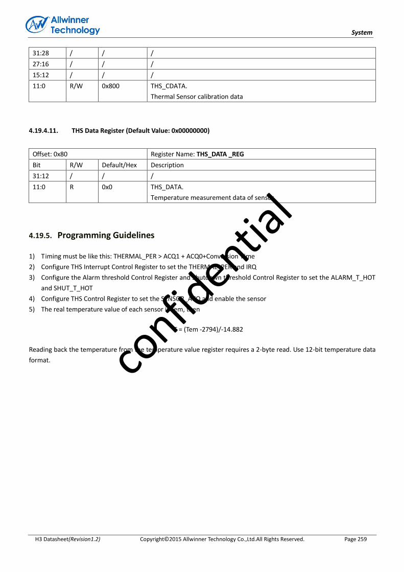
System
H3 Datasheet(Revision1.2) Copyright© 2015 Allwinner Technology Co.,Ltd.All Rights Reserved. Page 259
31:28 / / /
27:16 / / /
15:12 / / /
11:0 R/W 0x800 THS_CDATA.
Thermal Sensor calibration data
4.19.4.11. THS Data Register (Default Value: 0x00000000)
Offset: 0x80 Register Name: THS_DATA _REG
Bit R/W Default/Hex Description
31:12 / / /
11:0 R 0x0 THS_DATA.
Temperature measurement data of sensor
4.19.5. Programming Guidelines
1) Timing must be like this: THERMAL_PER > ACQ1 + ACQ0+Conversion Time
2) Configure THS Interrupt Control Register to set the THERMAL_PER and IRQ
3) Configure the Alarm threshold Control Register and Shutdown threshold Control Register to set the ALARM_T_HOT
and SHUT_T_HOT
4) Configure THS Control Register to set the SENSOR_ACQ and enable the sensor
5) The real temperature value of each sensor is Tem, then
T = (Tem -2794)/-14.882
Reading back the temperature from the temperature value register requires a 2-byte read. Use 12-bit temperature data
format. confid
ential
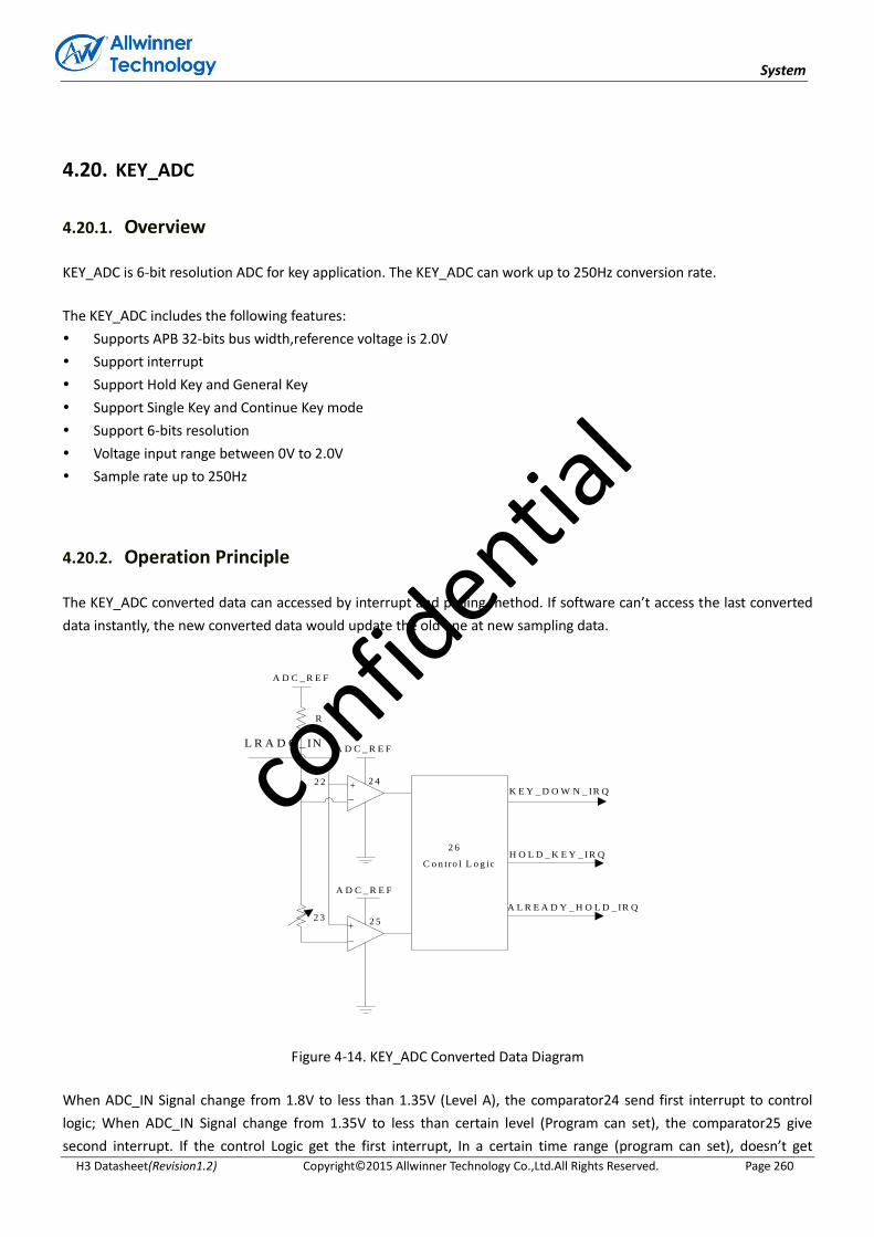
System
H3 Datasheet(Revision1.2) Copyright© 2015 Allwinner Technology Co.,Ltd.All Rights Reserved. Page 260
4.20. KEY_ADC
4.20.1. Overview
KEY_ADC is 6-bit resolution ADC for key application. The KEY_ADC can work up to 250Hz conversion rate.
The KEY_ADC includes the following features:
Supports APB 32-bits bus width,reference voltage is 2.0V
Support interrupt
Support Hold Key and General Key
Support Single Key and Continue Key mode
Support 6-bits resolution
Voltage input range between 0V to 2.0V
Sample rate up to 250Hz
4.20.2. Operation Principle
The KEY_ADC converted data can accessed by interrupt and polling method. If software can’t access the last converted
data instantly, the new converted data would update the old one at new sampling data.
R
2 2
2 3
A D C _ R E F
A D C _ R E F
A D C _ R E F
+_
_
+
C o n tro l L o g ic
K E Y _ D O W N _ IR Q
H O L D _ K E Y _ IR Q
A L R E A D Y _ H O L D _ IR Q
2 4
2 5
2 6
L R A D C _ IN
Figure 4-14. KEY_ADC Converted Data Diagram
When ADC_IN Signal change from 1.8V to less than 1.35V (Level A), the comparator24 send first interrupt to control
logic; When ADC_IN Signal change from 1.35V to less than certain level (Program can set), the comparator25 give
second interrupt. If the control Logic get the first interrupt, In a certain time range (program can set), doesn’t get
confid
ential
System
H3 Datasheet(Revision1.2) Copyright© 2015 Allwinner Technology Co.,Ltd.All Rights Reserved. Page 261
second interrupt, it will send hold key interrupt to the host; If the control Logic get the first interrupt, In a certain time
range (program can set), get second interrupt, it will send key down interrupt to the host; If the control logic only get
the second interrupt, doesn’t get the first interrupt, it will send already hold interrupt to the host.
The KEY_ADC have three mode, Normal Mode、Single Mode and Continue Mode. Normal mode is that the KEY_ADC will
report the result data of each convert all the time when the key is down. Single Mode is that the KEY_ADC will only
report the first convert result data when the key is down. Continue Mode is that the KEY_ADC will report one of 8*(N+1)
(N is program can set) sample convert result data when key is down.
The KEY_ADC is support four sample rate such as 250Hz、125Hz、62.5Hz and 32.25Hz, you can configure the value of
KEY_ADC_SAMPLE_RATE to select the fit sample rate.
4.20.3. KEY_ADC Register List
Module Name Base Address
KEY_ADC 0x01C21800
Register Name Offset Description
KEY_ADC_CTRL 0x00 KEY_ADC Control Register
KEY_ADC_INTC 0x04 KEY_ADC Interrupt Control Register
KEY_ADC_INTS 0x08 KEY_ADC Interrupt Status Register
KEY_ADC_DATA 0x0C KEY_ADC Data Register
4.20.4. KEY_ADC Register Description
4.20.4.1. KEY_ADC Control Register (Default Value: 0x01000168)
Offset: 0x00 Register Name: KEY_ADC_CTRL_REG
Bit R/W Default/Hex Description
31: 24 R/W 0x1 FIRST_CONVERT_DLY.
ADC First Convert Delay setting, ADC conversion is delayed by n samples
23:22 R/W 0x0 Reserved to 0
21:20 / / /
19:16 R/W 0x0 CONTINUE_TIME_SELECT.
Continue Mode time select, one of 8*(N+1) sample as a valuable sample
data
15:14 / / /
13:12 R/W 0x0 KEY_MODE_SELECT.
Key Mode Select:
00: Normal Mode
01: Single Mode
confid
ential
System
H3 Datasheet(Revision1.2) Copyright© 2015 Allwinner Technology Co.,Ltd.All Rights Reserved. Page 262
10: Continue Mode
11:8 R/W 0x1 LEVELA_B_CNT.
Level A to Level B time threshold select, judge ADC convert value in level A
to level B in n+1 samples
7 R/W 0X0 KEY_ADC_HOLD_KEY_EN
KEY_ADC Hold Key Enable
0: Disable
1: Enable
6 R/W 0x1 KEY_ADC_HOLD_EN.
KEY_ADC Sample hold Enable
0: Disable
1: Enable
5: 4 R/W 0x2 LEVELB_VOL.
Level B Corresponding Data Value setting (the real voltage value)
00: 0x3C (~1.9v)
01: 0x39 (~1.8v)
10: 0x36 (~1.7v)
11: 0x33 (~1.6v)
3: 2 R/W 0x2 KEY_ADC_SAMPLE_RATE.
KEY_ADC Sample Rate
00: 250 Hz
01: 125 Hz
10: 62.5 Hz
11: 32.25 Hz
1 / / /
0 R/W 0x0 KEY_ADC_EN.
KEY_ADC enable
0: Disable
1: Enable
4.20.4.2. KEY_ADC Interrupt Control Register (Default Value: 0x00000000)
Offset: 0x04 Register Name: KEY_ADC_INTC_REG
Bit R/W Default/Hex Description
31:5 / / /
4 R/W 0x0 ADC_KEYUP_IRQ_EN.
ADC Key Up IRQ Enable
0: Disable
1: Enable
3 R/W 0x0 ADC_ALRDY_HOLD_IRQ_EN.
ADC Already Hold IRQ Enable
0: Disable
1: Enable
2 R/W 0x0 ADC_HOLD_IRQ_EN.
confid
ential
System
H3 Datasheet(Revision1.2) Copyright© 2015 Allwinner Technology Co.,Ltd.All Rights Reserved. Page 263
ADC Hold Key IRQ Enable
0: Disable
1: Enable
1 R/W 0x0 ADC_KEYDOWN_EN
ADC Key Down Enable
0: Disable
1: Enable
0 R/W 0x0 ADC_DATA_IRQ_EN.
ADC Data IRQ Enable
0: Disable
1: Enable
4.20.4.3. KEY_ADC Interrupt Status Register (Default Value: 0x00000000)
Offset: 0x08 Register Name:KEY_ADC_INTS_REG
Bit R/W Default/Hex Description
31:5 / / /
4 R/W 0x0 ADC_KEYUP_PENDING.
ADC Key up pending Bit
When general key pull up, it the corresponding interrupt is enabled.
0: No IRQ
1: IRQ Pending
Notes: Writing 1 to the bit will clear it and its corresponding interrupt if the
interrupt is enable
3 R/W 0x0 ADC_ALRDY_HOLD_PENDING.
ADC Already Hold Pending Bit
When hold key pull down and pull the general key down, if the
corresponding interrupt is enabled.
0: No IRQ
1: IRQ Pending
Notes: Writing 1 to the bit will clear it and its corresponding interrupt if the
interrupt is enable
2 R/W 0x0 ADC_HOLDKEY_PENDING.
ADC Hold Key pending Bit
When Hold key pull down, the status bit is set and the interrupt line is set if
the corresponding interrupt is enabled.
0: NO IRQ
1: IRQ Pending
Notes: Writing 1 to the bit will clear it and its corresponding interrupt if the
interrupt is enable.
1 R/W 0x0 ADC_KEYDOWN_PENDING.
ADC Key Down IRQ Pending Bit
When General key pull down, the status bit is set and the interrupt line is
set if the corresponding interrupt is enabled.
confid
ential
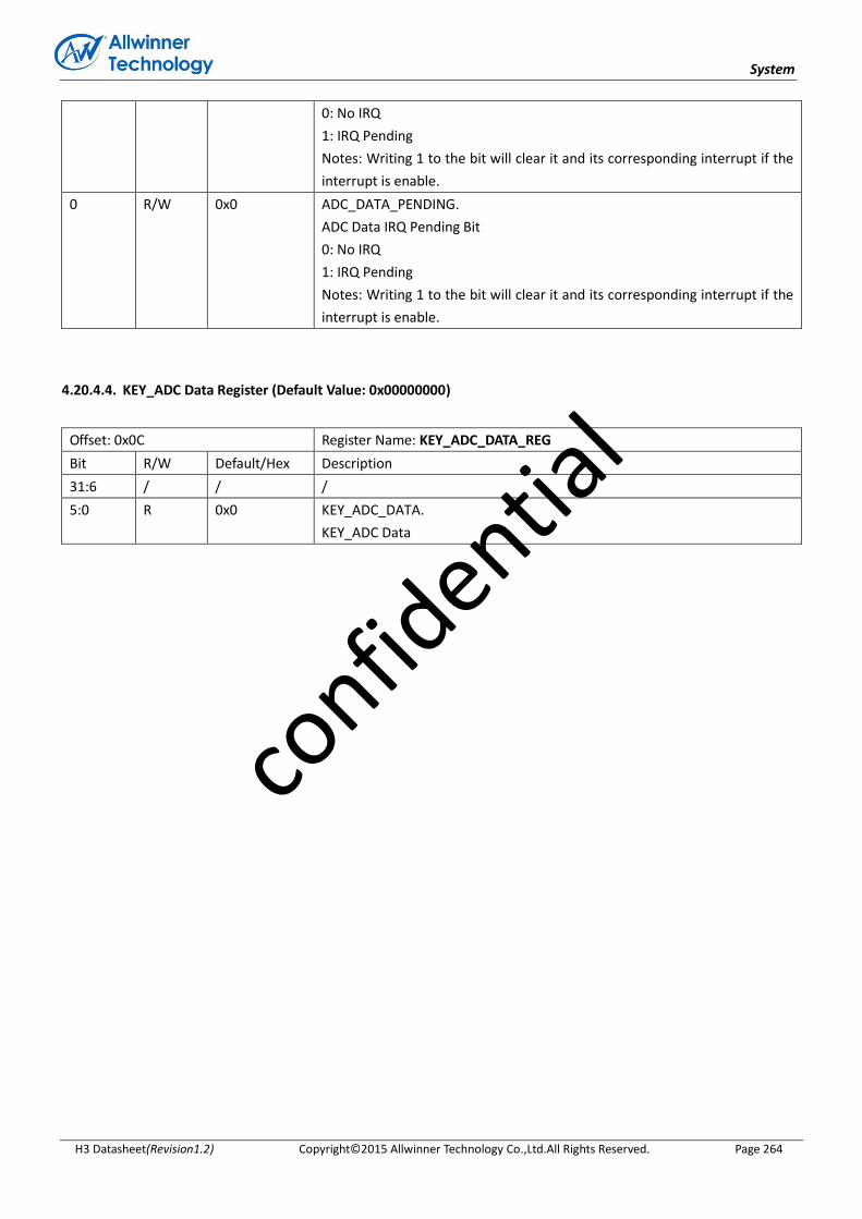
System
H3 Datasheet(Revision1.2) Copyright© 2015 Allwinner Technology Co.,Ltd.All Rights Reserved. Page 264
0: No IRQ
1: IRQ Pending
Notes: Writing 1 to the bit will clear it and its corresponding interrupt if the
interrupt is enable.
0 R/W 0x0 ADC_DATA_PENDING.
ADC Data IRQ Pending Bit
0: No IRQ
1: IRQ Pending
Notes: Writing 1 to the bit will clear it and its corresponding interrupt if the
interrupt is enable.
4.20.4.4. KEY_ADC Data Register (Default Value: 0x00000000)
Offset: 0x0C Register Name: KEY_ADC_DATA_REG
Bit R/W Default/Hex Description
31:6 / / /
5:0 R 0x0 KEY_ADC_DATA.
KEY_ADC Data
confid
ential
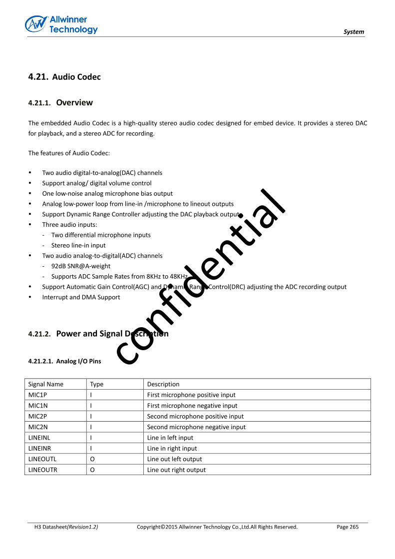
System
H3 Datasheet(Revision1.2) Copyright© 2015 Allwinner Technology Co.,Ltd.All Rights Reserved. Page 265
4.21. Audio Codec
4.21.1. Overview
The embedded Audio Codec is a high-quality stereo audio codec designed for embed device. It provides a stereo DAC
for playback, and a stereo ADC for recording.
The features of Audio Codec:
Two audio digital-to-analog(DAC) channels
Support analog/ digital volume control
One low-noise analog microphone bias output
Analog low-power loop from line-in /microphone to lineout outputs
Support Dynamic Range Controller adjusting the DAC playback output
Three audio inputs:
- Two differential microphone inputs
- Stereo line-in input
Two audio analog-to-digital(ADC) channels
- 92dB SNR@A-weight
- Supports ADC Sample Rates from 8KHz to 48KHz
Support Automatic Gain Control(AGC) and Dynamic Range Control(DRC) adjusting the ADC recording output
Interrupt and DMA Support
4.21.2. Power and Signal Description
4.21.2.1. Analog I/O Pins
Signal Name Type Description
MIC1P I First microphone positive input
MIC1N I First microphone negative input
MIC2P I Second microphone positive input
MIC2N I Second microphone negative input
LINEINL I Line in left input
LINEINR I Line in right input
LINEOUTL O Line out left output
LINEOUTR O Line out right output
confid
ential

System
H3 Datasheet(Revision1.2) Copyright© 2015 Allwinner Technology Co.,Ltd.All Rights Reserved. Page 266
4.21.2.2. Filter/Reference
MBIAS O Bias voltage output for main microphone
VRA1 O internal reference voltage
VRA2 O internal reference voltage
VRP O internal reference voltage
4.21.2.3. Power/Ground
AVCC P Analog power
AGND G Analog ground
4.21.3. Data Path Diagram
+
-
+
-
G
G
G
G
+
MM
+ GMMM
MM
+ GMMM
+
M M M M M M
M
M
ADC_R
ADC_L
DAC_L
DAC_R
M
M-1
G
M
LINEOUTR
LINEOUTL
LINEINL
LINEINR
MIC1P
MIC1N
MIC2P
MIC2N
SYSTEM BUS
2.5V
MICBIASENMICBIAS
G
M
M
Figure 4-15. Audio Codec Data Path Diagram
4.21.4. Audio Codec Register List
Module Name Base Address
AC 0X01C22C00
Register Name Offset Description
AC_DAC_DPC 0x000 DAC Digital Part Control Register
AC_DAC_FIFOC 0x004 DAC FIFO Control Register
confid
ential
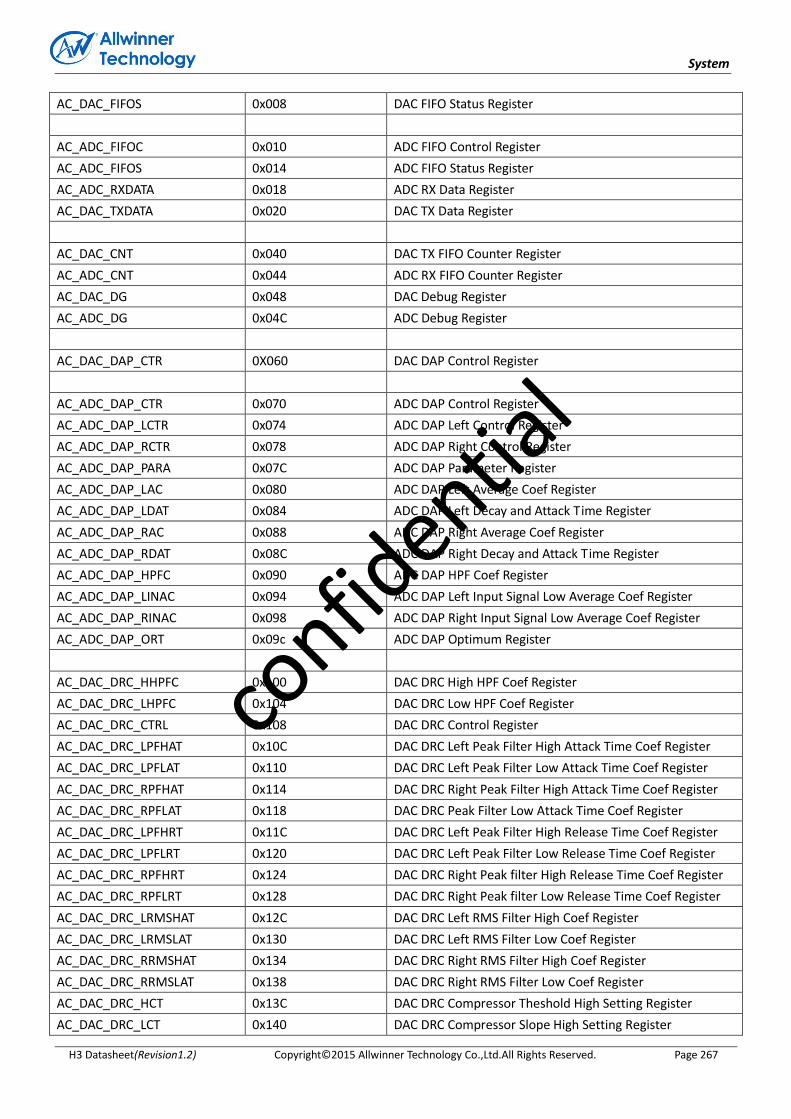
System
H3 Datasheet(Revision1.2) Copyright© 2015 Allwinner Technology Co.,Ltd.All Rights Reserved. Page 267
AC_DAC_FIFOS 0x008 DAC FIFO Status Register
AC_ADC_FIFOC 0x010 ADC FIFO Control Register
AC_ADC_FIFOS 0x014 ADC FIFO Status Register
AC_ADC_RXDATA 0x018 ADC RX Data Register
AC_DAC_TXDATA 0x020 DAC TX Data Register
AC_DAC_CNT 0x040 DAC TX FIFO Counter Register
AC_ADC_CNT 0x044 ADC RX FIFO Counter Register
AC_DAC_DG 0x048 DAC Debug Register
AC_ADC_DG 0x04C ADC Debug Register
AC_DAC_DAP_CTR 0X060 DAC DAP Control Register
AC_ADC_DAP_CTR 0x070 ADC DAP Control Register
AC_ADC_DAP_LCTR 0x074 ADC DAP Left Control Register
AC_ADC_DAP_RCTR 0x078 ADC DAP Right Control Register
AC_ADC_DAP_PARA 0x07C ADC DAP Parameter Register
AC_ADC_DAP_LAC 0x080 ADC DAP Left Average Coef Register
AC_ADC_DAP_LDAT 0x084 ADC DAP Left Decay and Attack Time Register
AC_ADC_DAP_RAC 0x088 ADC DAP Right Average Coef Register
AC_ADC_DAP_RDAT 0x08C ADC DAP Right Decay and Attack Time Register
AC_ADC_DAP_HPFC 0x090 ADC DAP HPF Coef Register
AC_ADC_DAP_LINAC 0x094 ADC DAP Left Input Signal Low Average Coef Register
AC_ADC_DAP_RINAC 0x098 ADC DAP Right Input Signal Low Average Coef Register
AC_ADC_DAP_ORT 0x09c ADC DAP Optimum Register
AC_DAC_DRC_HHPFC 0x100 DAC DRC High HPF Coef Register
AC_DAC_DRC_LHPFC 0x104 DAC DRC Low HPF Coef Register
AC_DAC_DRC_CTRL 0x108 DAC DRC Control Register
AC_DAC_DRC_LPFHAT 0x10C DAC DRC Left Peak Filter High Attack Time Coef Register
AC_DAC_DRC_LPFLAT 0x110 DAC DRC Left Peak Filter Low Attack Time Coef Register
AC_DAC_DRC_RPFHAT 0x114 DAC DRC Right Peak Filter High Attack Time Coef Register
AC_DAC_DRC_RPFLAT 0x118 DAC DRC Peak Filter Low Attack Time Coef Register
AC_DAC_DRC_LPFHRT 0x11C DAC DRC Left Peak Filter High Release Time Coef Register
AC_DAC_DRC_LPFLRT 0x120 DAC DRC Left Peak Filter Low Release Time Coef Register
AC_DAC_DRC_RPFHRT 0x124 DAC DRC Right Peak filter High Release Time Coef Register
AC_DAC_DRC_RPFLRT 0x128 DAC DRC Right Peak filter Low Release Time Coef Register
AC_DAC_DRC_LRMSHAT 0x12C DAC DRC Left RMS Filter High Coef Register
AC_DAC_DRC_LRMSLAT 0x130 DAC DRC Left RMS Filter Low Coef Register
AC_DAC_DRC_RRMSHAT 0x134 DAC DRC Right RMS Filter High Coef Register
AC_DAC_DRC_RRMSLAT 0x138 DAC DRC Right RMS Filter Low Coef Register
AC_DAC_DRC_HCT 0x13C DAC DRC Compressor Theshold High Setting Register
AC_DAC_DRC_LCT 0x140 DAC DRC Compressor Slope High Setting Register
confid
ential

System
H3 Datasheet(Revision1.2) Copyright© 2015 Allwinner Technology Co.,Ltd.All Rights Reserved. Page 268
AC_DAC_DRC_HKC 0x144 DAC DRC Compressor Slope High Setting Register
AC_DAC_DRC_LKC 0x148 DAC DRC Compressor Slope Low Setting Register
AC_DAC_DRC_HOPC 0x14C
DAC DRC Compressor High Output at Compressor Threshold
Register
AC_DAC_DRC_LOPC 0x150
DAC DRC Compressor Low Output at Compressor Threshold
Register
AC_DAC_DRC_HLT 0x154 DAC DRC Limiter Theshold High Setting Register
AC_DAC_DRC_LLT 0x158 DAC DRC Limiter Theshold Low Setting Register
AC_DAC_DRC_HKl 0x15C DAC DRC Limiter Slope High Setting Register
AC_DAC_DRC_LKl 0x160 DAC DRC Limiter Slope Low Setting Register
AC_DAC_DRC_HOPL 0x164 DAC DRC Limiter High Output at Limiter Threshold
AC_DAC_DRC_LOPL 0x168 DAC DRC Limiter Low Output at Limiter Threshold
AC_DAC_DRC_HET 0x16C DAC DRC Expander Theshold High Setting Register
AC_DAC_DRC_LET 0x170 DAC DRC Expander Theshold Low Setting Register
AC_DAC_DRC_HKE 0x174 DAC DRC Expander Slope High Setting Register
AC_DAC_DRC_LKE 0x178 DAC DRC Expander Slope Low Setting Register
AC_DAC_DRC_HOPE 0x17C DAC DRC Expander High Output at Expander Threshold
AC_DAC_DRC_LOPE 0x180 DAC DRC Expander Low Output at Expander Threshold
AC_DAC_DRC_HKN 0x184 DAC DRC Linear Slope High Setting Register
AC_DAC_DRC_LKN 0x188 DAC DRC Linear Slope Low Setting Register
AC_DAC_DRC_SFHAT 0x18C DAC DRC Smooth filter Gain High Attack Time Coef Register
AC_DAC_DRC_SFLAT 0x190 DAC DRC Smooth filter Gain Low Attack Time Coef Register
AC_DAC_DRC_SFHRT 0x194
DAC DRC Smooth filter Gain High Release Time Coef
Register
AC_DAC_DRC_SFLRT 0x198 DAC DRC Smooth filter Gain Low Release Time Coef Register
AC_DAC_DRC_MXGHS 0x19C DAC DRC MAX Gain High Setting Register
AC_DAC_DRC_MXGLS 0x1A0 DAC DRC MAX Gain Low Setting Register
AC_DAC_DRC_MNGHS 0x1A4 DAC DRC MIN Gain High Setting Register
AC_DAC_DRC_MNGLS 0x1A8 DAC DRC MIN Gain Low Setting Register
AC_DAC_DRC_EPSHC 0x1AC DAC DRC Expander Smooth Time High Coef Register
AC_DAC_DRC_EPSLC 0x1B0 DAC DRC Expander Smooth Time Low Coef Register
AC_DAC_DRC_OPT 0x1B4 DAC DRC Optimum Register
AC_DAC_DRC_HPFHGAIN 0x1B8 DAC DRC HPF Gain High Coef Register
AC_DAC_DRC_HPFLGAIN 0x1BC DAC DRC HPF Gain Low Coef Register
AC_ADC_DRC_HHPFC 0x200 ADC DRC High HPF Coef Register
AC_ADC_DRC_LHPFC 0x204 ADC DRC Low HPF Coef Register
AC_ADC_DRC_CTRL 0x208 ADC DRC Control Register
AC_ADC_DRC_LPFHAT 0x20C ADC DRC Left Peak Filter High Attack Time Coef Register
AC_ADC_DRC_LPFLAT 0x210 ADC DRC Left Peak Filter Low Attack Time Coef Register
AC_ADC_DRC_RPFHAT 0x214 ADC DRC Right Peak Filter High Attack Time Coef Register
AC_ADC_DRC_RPFLAT 0x218 ADC DRC Peak Filter Low Attack Time Coef Register
AC_ADC_DRC_LPFHRT 0x21C ADC DRC Left Peak Filter High Release Time Coef Register
AC_ADC_DRC_LPFLRT 0x220 ADC DRC Left Peak Filter Low Release Time Coef Register
confid
ential

System
H3 Datasheet(Revision1.2) Copyright© 2015 Allwinner Technology Co.,Ltd.All Rights Reserved. Page 269
AC_ADC_DRC_RPFHRT 0x224 ADC DRC Right Peak filter High Release Time Coef Register
AC_ADC_DRC_RPFLRT 0x228 ADC DRC Right Peak filter Low Release Time Coef Register
AC_ADC_DRC_LRMSHAT 0x22C ADC DRC Left RMS Filter High Coef Register
AC_ADC_DRC_LRMSLAT 0x230 ADC DRC Left RMS Filter Low Coef Register
AC_ADC_DRC_RRMSHAT 0x234 ADC DRC Right RMS Filter High Coef Register
AC_ADC_DRC_RRMSLAT 0x238 ADC DRC Right RMS Filter Low Coef Register
AC_ADC_DRC_HCT 0x23C ADC DRC Compressor Theshold High Setting Register
AC_ADC_DRC_LCT 0x240 ADC DRC Compressor Slope High Setting Register
AC_ADC_DRC_HKC 0x244 ADC DRC Compressor Slope High Setting Register
AC_ADC_DRC_LKC 0x248 ADC DRC Compressor Slope Low Setting Register
AC_ADC_DRC_HOPC 0x24C
ADC DRC Compressor High Output at Compressor Threshold
Register
AC_ADC_DRC_LOPC 0x250
ADC DRC Compressor Low Output at Compressor Threshold
Register
AC_ADC_DRC_HLT 0x254 ADC DRC Limiter Theshold High Setting Register
AC_ADC_DRC_LLT 0x258 ADC DRC Limiter Theshold Low Setting Register
AC_ADC_DRC_HKl 0x25C ADC DRC Limiter Slope High Setting Register
AC_ADC_DRC_LKl 0x260 ADC DRC Limiter Slope Low Setting Register
AC_ADC_DRC_HOPL 0x264 ADC DRC Limiter High Output at Limiter Threshold
AC_ADC_DRC_LOPL 0x268 ADC DRC Limiter Low Output at Limiter Threshold
AC_ADC_DRC_HET 0x26C ADC DRC Expander Theshold High Setting Register
AC_ADC_DRC_LET 0x270 ADC DRC Expander Theshold Low Setting Register
AC_ADC_DRC_HKE 0x274 ADC DRC Expander Slope High Setting Register
AC_ADC_DRC_LKE 0x278 ADC DRC Expander Slope Low Setting Register
AC_ADC_DRC_HOPE 0x27C ADC DRC Expander High Output at Expander Threshold
AC_ADC_DRC_LOPE 0x280 ADC DRC Expander Low Output at Expander Threshold
AC_ADC_DRC_HKN 0x284 ADC DRC Linear Slope High Setting Register
AC_ADC_DRC_LKN 0x288 ADC DRC Linear Slope Low Setting Register
AC_ADC_DRC_SFHAT 0x28C ADC DRC Smooth filter Gain High Attack Time Coef Register
AC_ADC_DRC_SFLAT 0x290 ADC DRC Smooth filter Gain Low Attack Time Coef Register
AC_ADC_DRC_SFHRT 0x294
ADC DRC Smooth filter Gain High Release Time Coef
Register
AC_ADC_DRC_SFLRT 0x298 ADC DRC Smooth filter Gain Low Release Time Coef Register
AC_ADC_DRC_MXGHS 0x29C ADC DRC MAX Gain High Setting Register
AC_ADC_DRC_MXGLS 0x2A0 ADC DRC MAX Gain Low Setting Register
AC_ADC_DRC_MNGLS 0x2A4 ADC DRC MIN Gain High Setting Register
AC_ADC_DRC_MXGLS 0x2A8 ADC DRC MIN Gain Low Setting Register
AC_ADC_DRC_EPSHC 0x2AC ADC DRC Expander Smooth Time High Coef Register
AC_ADC_DRC_EPSLC 0x2B0 ADC DRC Expander Smooth Time Low Coef Register
AC_ADC_DRC_OPT 0x2B4 ADC DRC Optimum Register
AC_ADC_DRC_HPFHGAIN 0x2B8 ADC DRC HPF Gain High Coef Register
AC_ADC_DRC_HPFLGAIN 0x2BC ADC DRC HPF Gain Low Coef Register
Analog Domain Register
confid
ential
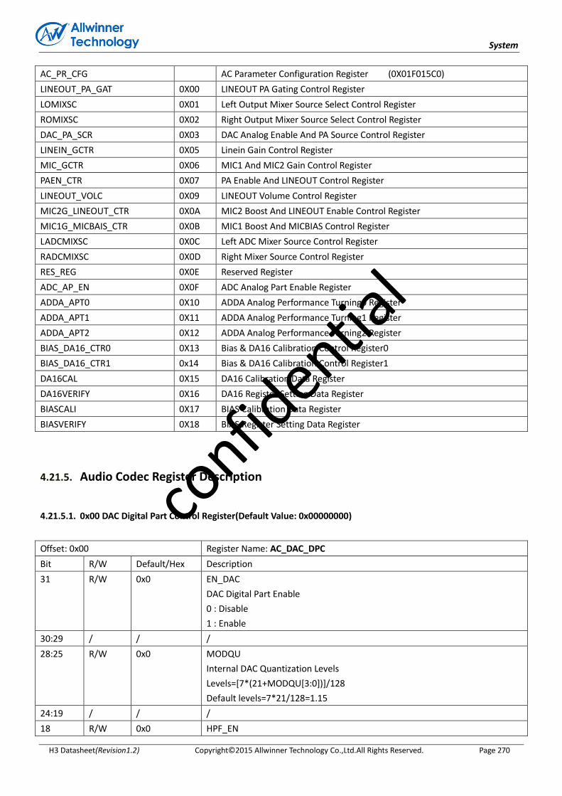
System
H3 Datasheet(Revision1.2) Copyright© 2015 Allwinner Technology Co.,Ltd.All Rights Reserved. Page 270
AC_PR_CFG AC Parameter Configuration Register (0X01F015C0)
LINEOUT_PA_GAT 0X00 LINEOUT PA Gating Control Register
LOMIXSC 0X01 Left Output Mixer Source Select Control Register
ROMIXSC 0X02 Right Output Mixer Source Select Control Register
DAC_PA_SCR 0X03 DAC Analog Enable And PA Source Control Register
LINEIN_GCTR 0X05 Linein Gain Control Register
MIC_GCTR 0X06 MIC1 And MIC2 Gain Control Register
PAEN_CTR 0X07 PA Enable And LINEOUT Control Register
LINEOUT_VOLC 0X09 LINEOUT Volume Control Register
MIC2G_LINEOUT_CTR 0X0A MIC2 Boost And LINEOUT Enable Control Register
MIC1G_MICBAIS_CTR 0X0B MIC1 Boost And MICBIAS Control Register
LADCMIXSC 0X0C Left ADC Mixer Source Control Register
RADCMIXSC 0X0D Right Mixer Source Control Register
RES_REG 0X0E Reserved Register
ADC_AP_EN 0X0F ADC Analog Part Enable Register
ADDA_APT0 0X10 ADDA Analog Performance Turning0 Register
ADDA_APT1 0X11 ADDA Analog Performance Turning1 Register
ADDA_APT2 0X12 ADDA Analog Performance Turning2 Register
BIAS_DA16_CTR0 0X13 Bias & DA16 Calibration Control Register0
BIAS_DA16_CTR1 0x14 Bias & DA16 Calibration Control Register1
DA16CAL 0X15 DA16 Calibration Data Register
DA16VERIFY 0X16 DA16 Register Setting Data Register
BIASCALI 0X17 BIAS Calibration Data Register
BIASVERIFY 0X18 BIAS Register Setting Data Register
4.21.5. Audio Codec Register Description
4.21.5.1. 0x00 DAC Digital Part Control Register(Default Value: 0x00000000)
Offset: 0x00 Register Name: AC_DAC_DPC
Bit R/W Default/Hex Description
31 R/W 0x0 EN_DAC
DAC Digital Part Enable
0 : Disable
1 : Enable
30:29 / / /
28:25 R/W 0x0 MODQU
Internal DAC Quantization Levels
Levels=[7*(21+MODQU[3:0])]/128
Default levels=7*21/128=1.15
24:19 / / /
18 R/W 0x0 HPF_EN
confid
ential
System
H3 Datasheet(Revision1.2) Copyright© 2015 Allwinner Technology Co.,Ltd.All Rights Reserved. Page 271
High Pass Filter Enable
0: Disable
1: Enable
17:12 R/W 0x0 DVOL
Digital volume control: DVC, ATT=DVC[5:0]*(-1.16Db)
64 steps, -1.16Db/step
11:1 / / /
0 R/W 0x0 HUB_EN
Audio Hub Enable
0: Disable
1: Enable
4.21.5.2. 0x04 DAC FIFO Control Register(Default Value: 0x00000F00)
Offset: 0x04 Register Name: AC_DAC_FIFOC
Bit R/W Default/Hex Description
31:29 R/W 0X0 DAC_FS
Sample Rate Of DAC
000: 48KHz
010: 24KHz
100: 12KHz
110: 192KHz
001: 32KHz
011: 16KHz
101: 8KHz
111: 96KHz
44.1KHz/22.05KHz/11.025KHz can be supported by Audio PLL Configure Bit
28 R/W 0x0 FIR_VER
FIR Version
0: 64-Tap FIR; 1: 32-Tap FIR
27 / / /
26 R/W 0x0 SEND_LASAT
Audio sample select when TX FIFO under run
0: Sending zero
1: Sending last audio sample
25:24 R/W 0x0 FIFO_MODE
For 24-bits transmitted audio sample:
00/10: FIFO_I[23:0] = {TXDATA[31:8]}
01/11: Reserved
For 16-bits transmitted audio sample:
00/10: FIFO_I[23:0] = {TXDATA[31:16], 8’b0}
01/11: FIFO_I[23:0] = {TXDATA[15:0], 8’b0}
23 / / /
22:21 R/W 0X0 DAC_DRQ_CLR_CNT
confid
ential
System
H3 Datasheet(Revision1.2) Copyright© 2015 Allwinner Technology Co.,Ltd.All Rights Reserved. Page 272
When TX FIFO Available Room Less Than Or Equal N, DRQ Request Will Be
De-Asserted. N Is Defined Here:
00: IRQ/DRQ De-Asserted When WLEVEL > TXTL
01: 4
10: 8
11: 16
20:15 / / /
14:8 R/W 0XF TX_TRIG_LEVEL
TX FIFO Empty Trigger Level (TXTL[12:0])
Interrupt and DMA request trigger level for TX FIFO normal condition.
IRQ/DRQ Generated when WLEVEL ≤ TXTL
Notes:
1. WLEVEL represents the number of valid samples in the TX FIFO
2. Only TXTL[6:0] valid when TXMODE = 0
7 R/W 0X0 ADDA_LOOP_EN
ADDA Loop Enable
0: Disable
1: Enable
6 R/W 0X0 DAC_MONO_EN
DAC Mono Enable
0: Stereo, 64 Levels FIFO
1: Mono, 128 Levels FIFO
When Enabled, L & R Channel Send Same Data
5 R/W 0X0 TX_SAMPLE_BITS
Transmitting Audio Sample Resolution
0: 16 bits
1: 24 bits
4 R/W 0X0 DAC_DRQ_EN
DAC FIFO Empty DRQ Enable
0: Disable
1: Enable
3 R/W 0X0 DAC_IRQ_EN
DAC FIFO Empty IRQ Enable
0: Disable
1: Enable
2 R/W 0X0 FIFO_UNDERRUN_IRQ_EN
DAC FIFO Under Run IRQ Enable
0: Disable
1: Enable
1 R/W 0X0 FIFO_OVERRUN_IRQ_EN
DAC FIFO Over Run IRQ Enable
0: Disable
1: Enable
0 R/W 0X0 FIFO_FLUSH
DAC FIFO Flush
confid
ential
System
H3 Datasheet(Revision1.2) Copyright© 2015 Allwinner Technology Co.,Ltd.All Rights Reserved. Page 273
Write ‘1’ To Flush TX FIFO, Self Clear to ‘0’
4.21.5.3. 0x08 DAC FIFO Status Register(Default Value: 0x00800088)
Offset: 0x08 Register Name: AC_DAC_FIFOS
Bit R/W Default/Hex Description
31:24 / / /
23 R 0x1 TX_EMPTY
TX FIFO Empty
0: No room for new sample in TX FIFO
1: More than one room for new sample in TX FIFO (>= 1 word)
22:8 R 0x80 TXE_CNT
TX FIFO Empty Space Word Counter
7:4 / / /
3 R/W 0x1 TXE_INT
TX FIFO Empty Pending Interrupt
0: No Pending IRQ
1: FIFO Empty Pending Interrupt
Write ‘1’ to clear this interrupt or automatic clear if interrupt condition fails
2 R/W 0x0 TXU_INT
TX FIFO Under run Pending Interrupt
0: No Pending Interrupt
1: FIFO Under run Pending Interrupt
Write ‘1’ to clear this interrupt
1 R/W 0x0 TXO_INT
TX FIFO Overrun Pending Interrupt
0: No Pending Interrupt
1: FIFO Overrun Pending Interrupt
Write ‘1’ to clear this interrupt
0 / / /
4.21.5.4. 0x10 ADC FIFO Control Register(Default Value: 0x00000F00)
Offset: 0x10 Register Name: AC_ADC_FIFOC
Bit R/W Default/Hex Description
31:29 R/W 0X0 ADFS
Sample Rate of ADC
000: 48KHz
010: 24KHz
100: 12KHz
110: Reserved
001: 32KHz
confid
ential

System
H3 Datasheet(Revision1.2) Copyright© 2015 Allwinner Technology Co.,Ltd.All Rights Reserved. Page 274
011: 16KHz
101: 8KHz
111: Reserved
44.1KHz/22.05KHz/11.025KHz can be supported by Audio PLL Configure Bit
28 R/W 0X0 EN_AD
ADC Digital Part Enable
0: Disable
1: Enable
27:25 / / /
24 R/W 0X0 RX_FIFO_MODE
RX FIFO Output Mode (Mode 0, 1)
0: Expanding ‘0’ at LSB of TX FIFO register
1: Expanding received sample sign bit at MSB of TX FIFO register
For 24-bits received audio sample:
Mode 0: RXDATA[31:0] = {FIFO_O[23:0], 8’h0}
Mode 1: Reserved
For 16-bits received audio sample:
Mode 0: RXDATA[31:0] = {FIFO_O[23:8], 16’h0}
Mode 1: RXDATA[31:0] = {16{FIFO_O[23]}, FIFO_O[23:8]}
23:19 / / /
18:17 R/W 0X0 ADCFDT
ADC FIFO Delay Time For writing Data after EN_AD
00:5ms
01:10ms
10:20ms
11:30ms
16 R/W 0X0 ADCDFEN
ADC FIFO Delay Function For writing Data after EN_AD
0: Disable
1: Enable
15:13 / / /
12:8 R/W 0XF RX_FIFO_TRG_LEVEL
RX FIFO Trigger Level (RXTL[4:0])
Interrupt and DMA request trigger level for RX FIFO normal condition
IRQ/DRQ Generated when WLEVEL < RXTL[4:0]
Notes:
WLEVEL represents the number of valid samples in the RX FIFO
7 R/W 0X0 ADC_MONO_EN
ADC Mono Enable
0: Stereo, 16 levels FIFO
1: mono, 32 levels FIFO
When set to ‘1’, Only left channel samples are recorded
6 R/W 0x0 RX_SAMPLE_BITS
Receiving Audio Sample Resolution
0: 16 bits
confid
ential

System
H3 Datasheet(Revision1.2) Copyright© 2015 Allwinner Technology Co.,Ltd.All Rights Reserved. Page 275
1: 24 bits
5 / / /
4 R/W 0X0 ADC_DRQ_EN
ADC FIFO Data Available DRQ Enable
0: Disable
1: Enable
3 R/W 0X0 ADC_IRQ_EN
ADC FIFO Data Available IRQ Enable
0: Disable
1: Enable
2 / /
1 R/W 0X0 ADC_OVERRUN_IRQ_EN
ADC FIFO Over Run IRQ Enable
0: Disable
1: Enable
0 R/W 0X0 ADC_FIFO_FLUSH
ADC FIFO Flush
Write ‘1’ to flush TX FIFO, self clear to ‘0’
4.21.5.5. 0x14 ADC FIFO Status Register(Default Value: 0x00000000)
Offset: 0x14 Register Name: AC_ADC_FIFOS
Bit R/W Default/Hex Description
31:24 / / /
23 R 0X0 RXA
RX FIFO Available
0: No available data in RX FIFO
1: More than one sample in RX FIFO (>= 1 word)
22:14 / / /
13:8 R 0X0 RXA_CNT
RX FIFO Available Sample Word Counter
7:4 / / /
3 R/W 0X0 RXA_INT
RX FIFO Data Available Pending Interrupt
0: No Pending IRQ
1: Data Available Pending IRQ
Write ‘1’ to clear this interrupt or automatic clear if interrupt condition fails
2 / / /
1 R/W 0X0 RXO_INT
RX FIFO Overrun Pending Interrupt
0: No Pending IRQ
1: FIFO Overrun Pending IRQ
Write ‘1’ to clear this interrupt
confid
ential

System
H3 Datasheet(Revision1.2) Copyright© 2015 Allwinner Technology Co.,Ltd.All Rights Reserved. Page 276
0 / / /
4.21.5.6. 0x18 ADC RX DATA Register(Default Value: 0x00000000)
Offset: 0x18 Register Name: AC_ADC_RXDATA
Bit R/W Default/Hex Description
31:0 R 0X0 RX_DATA
RX Sample
Host can get one sample by reading this register. The left channel sample data
is first and then the right channel sample.
4.21.5.7. 0x20 DAC TX DATA Register(Default Value: 0x00000000)
Offset: 0x20 Register Name: AC_DAC_TXDATA
Bit R/W Default/Hex Description
31:0 W 0X0 TX_DATA
Transmitting left, right channel sample data should be written this register
one by one. The left channel sample data is first and then the right channel
sample
4.21.5.8. 0x40 DAC TX Counter Register(Default Value: 0x00000000)
Offset: 0x40 Register Name: AC_DAC_CNT
Bit R/W Default/Hex Description
31:0 R/W 0X0 TX_CNT
TX Sample Counter
The audio sample number of sending into TXFIFO. When one sample is put
into TXFIFO by DMA or by host IO, the TX sample counter register increases by
one. The TX sample counter register can be set to any initial valve at any time.
After been updated by the initial value, the counter register should count on
base of this initial value
Notes: It is used for Audio/ Video Synchronization
4.21.5.9. 0x44 ADC RX Counter Register(Default Value: 0x00000000)
Offset: 0x44 Register Name: AC_ADC_CNT
Bit R/W Default/Hex Description
31:0 R/W 0X0 RX_CNT
RX Sample Counter
confid
ential
System
H3 Datasheet(Revision1.2) Copyright© 2015 Allwinner Technology Co.,Ltd.All Rights Reserved. Page 277
The audio sample number of writing into RXFIFO. When one sample is written
by Digital Audio Engine, the RX sample counter register increases by one. The
RX sample counter register can be set to any initial valve at any time. After
been updated by the initial value, the counter register should count on base
of this initial value
Notes: It is used for Audio/ Video Synchronization
4.21.5.10. 0x48 DAC Debug Register(Default Value: 0x00000000)
Offset: 0x48 Register Name: AC_DAC_DG
Bit R/W Default/Hex Description
31:12 / / /
11 R/W 0X0 DAC_MODU_SELECT
DAC Modulator Debug
0: DAC Modulator Normal Mode
1: DAC Modulator Debug Mode
10:9 R/W 0X0 DAC_PATTERN_SELECT.
DAC Pattern Select
00: Normal (Audio Sample from TX FIFO)
01: -6 dB Sin wave
10: -60 dB Sin wave
11: silent wave
8 R/W 0X0 CODEC_CLK_SELECT
CODEC Clock Source Select
0: CODEC Clock from PLL
1: CODEC Clock from OSC (For Debug)
7 / / /
6 R/W 0X0 DA_SWP
DAC output channel swap enable
0:Disable
1:Enable
5:0 / / /
4.21.5.11. 0x4C ADC Debug Register(Default Value: 0x00000000)
Offset: 0x4C Register Name: AC_ADC_DG
Bit R/W Default/Hex Description
31:25 / / /
24 R/W 0X0 AD_SWP
ADC Output Channel Swap Enable (for digital filter)
0: Disable
1: Enable
confid
ential
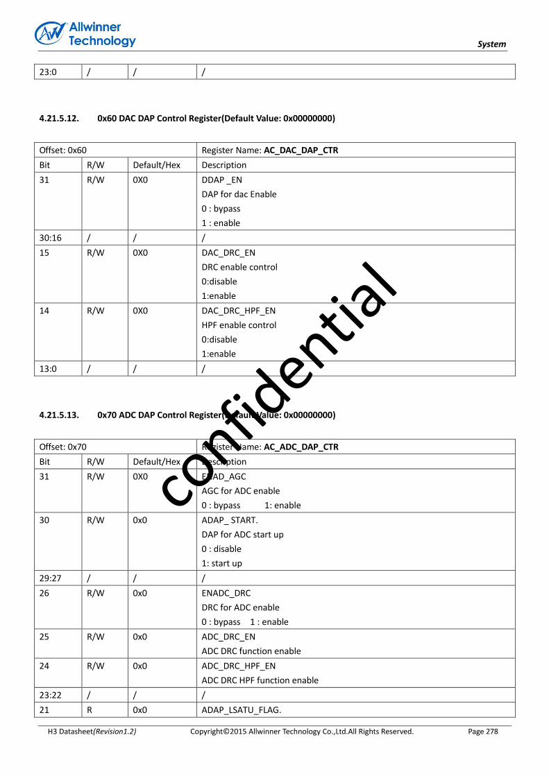
System
H3 Datasheet(Revision1.2) Copyright© 2015 Allwinner Technology Co.,Ltd.All Rights Reserved. Page 278
23:0 / / /
4.21.5.12. 0x60 DAC DAP Control Register(Default Value: 0x00000000)
Offset: 0x60 Register Name: AC_DAC_DAP_CTR
Bit R/W Default/Hex Description
31 R/W 0X0 DDAP _EN
DAP for dac Enable
0 : bypass
1 : enable
30:16 / / /
15 R/W 0X0 DAC_DRC_EN
DRC enable control
0:disable
1:enable
14 R/W 0X0 DAC_DRC_HPF_EN
HPF enable control
0:disable
1:enable
13:0 / / /
4.21.5.13. 0x70 ADC DAP Control Register(Default Value: 0x00000000)
Offset: 0x70 Register Name: AC_ADC_DAP_CTR
Bit R/W Default/Hex Description
31 R/W 0X0 ENAD_AGC
AGC for ADC enable
0 : bypass 1: enable
30 R/W 0x0 ADAP_ START.
DAP for ADC start up
0 : disable
1: start up
29:27 / / /
26 R/W 0x0 ENADC_DRC
DRC for ADC enable
0 : bypass 1 : enable
25 R/W 0x0 ADC_DRC_EN
ADC DRC function enable
24 R/W 0x0 ADC_DRC_HPF_EN
ADC DRC HPF function enable
23:22 / / /
21 R 0x0 ADAP_LSATU_FLAG.
confid
ential

System
H3 Datasheet(Revision1.2) Copyright© 2015 Allwinner Technology Co.,Ltd.All Rights Reserved. Page 279
Left channel AGC saturation flag
0 : no saturation
1: saturation
20 R 0x0 ADAP_LNOI_FLAG.
Left channel AGC noise-threshold flag
0: no noise-threshold
1: noise-threshold
19:12 R 0x0 ADAP_LCHAN_GAIN
Left channel Gain applied by AGC
(7.1format 2s component(-20dB – 40dB), 0.5dB/ step)
0x50 : 40dB
0x4F : 39.5dB
---------------
0x00 : 00dB
0xFF : -0.5dB
11:10 / / /
9 R 0x0 ADAP_RSATU_FLAG.
Right AGC saturation flag
0 : no saturation
1: saturation
8 R 0x0 ADAP_RNOI_FLAG.
Right channel AGC noise-threshold flag
0:
1:
7:0 R 0x0 ADAP_LCHAN_GAIN.
Right Channel Gain applied by AGC (7.1format 2s component)(0.5dB step)
0x50 : 40dB
0x4F : 39.5dB
---------------
0x00 : 00dB
0xFF : -0.5dB
4.21.5.14. 0x74 ADC DAP Left Control Register(Default Value: 0x001F7000)
Offset: 0x74 Register Name: AC_ADC_DAP_LCTR
Bit R/W Default/Hex Description
31:24 / / /
23:16 R/W 0x1F
(-86dB)
ADAP_LNOI_SET.
Left channel noise threshold setting
0x00 : -24dB
0x01 : -26dB
0x02 : -28dB
----------------------
0x1D: -82dB
confid
ential
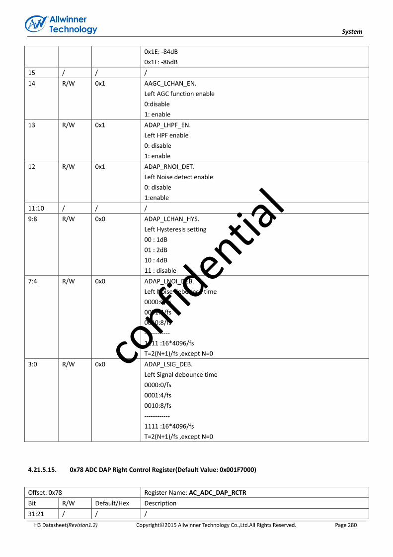
System
H3 Datasheet(Revision1.2) Copyright© 2015 Allwinner Technology Co.,Ltd.All Rights Reserved. Page 280
0x1E: -84dB
0x1F: -86dB
15 / / /
14 R/W 0x1 AAGC_LCHAN_EN.
Left AGC function enable
0:disable
1: enable
13 R/W 0x1 ADAP_LHPF_EN.
Left HPF enable
0: disable
1: enable
12 R/W 0x1 ADAP_RNOI_DET.
Left Noise detect enable
0: disable
1:enable
11:10 / / /
9:8 R/W 0x0 ADAP_LCHAN_HYS.
Left Hysteresis setting
00 : 1dB
01 : 2dB
10 : 4dB
11 : disable
7:4 R/W 0x0 ADAP_LNOI_DEB.
Left Noise debounce time
0000:0/fs
0001:4/fs
0010:8/fs
------------
1111 :16*4096/fs
T=2(N+1)/fs ,except N=0
3:0 R/W 0x0 ADAP_LSIG_DEB.
Left Signal debounce time
0000:0/fs
0001:4/fs
0010:8/fs
------------
1111 :16*4096/fs
T=2(N+1)/fs ,except N=0
4.21.5.15. 0x78 ADC DAP Right Control Register(Default Value: 0x001F7000)
Offset: 0x78 Register Name: AC_ADC_DAP_RCTR
Bit R/W Default/Hex Description
31:21 / / /
confid
ential
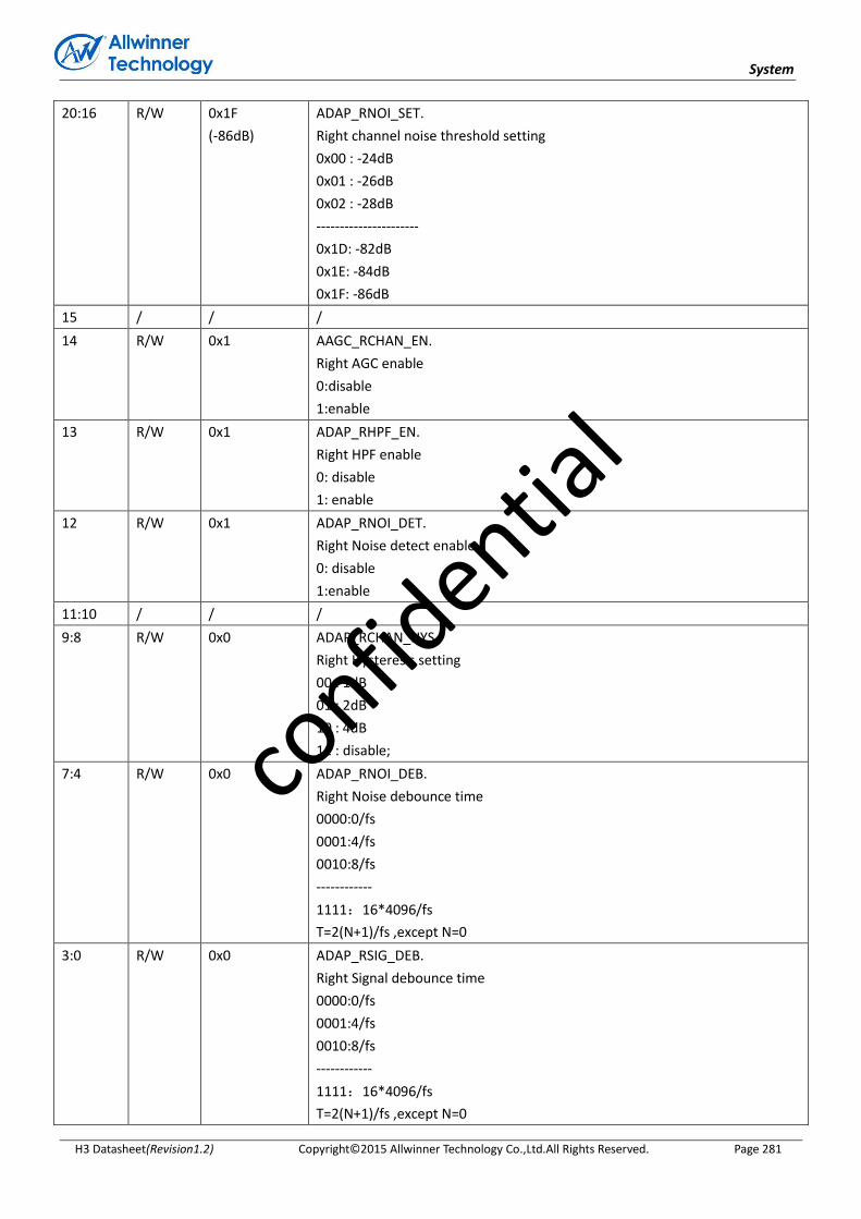
System
H3 Datasheet(Revision1.2) Copyright© 2015 Allwinner Technology Co.,Ltd.All Rights Reserved. Page 281
20:16 R/W 0x1F
(-86dB)
ADAP_RNOI_SET.
Right channel noise threshold setting
0x00 : -24dB
0x01 : -26dB
0x02 : -28dB
----------------------
0x1D: -82dB
0x1E: -84dB
0x1F: -86dB
15 / / /
14 R/W 0x1 AAGC_RCHAN_EN.
Right AGC enable
0:disable
1:enable
13 R/W 0x1 ADAP_RHPF_EN.
Right HPF enable
0: disable
1: enable
12 R/W 0x1 ADAP_RNOI_DET.
Right Noise detect enable
0: disable
1:enable
11:10 / / /
9:8 R/W 0x0 ADAP_RCHAN_HYS.
Right Hysteresis setting
00 : 1dB
01 : 2dB
10 : 4dB
11 : disable;
7:4 R/W 0x0 ADAP_RNOI_DEB.
Right Noise debounce time
0000:0/fs
0001:4/fs
0010:8/fs
------------
1111:16*4096/fs
T=2(N+1)/fs ,except N=0
3:0 R/W 0x0 ADAP_RSIG_DEB.
Right Signal debounce time
0000:0/fs
0001:4/fs
0010:8/fs
------------
1111:16*4096/fs
T=2(N+1)/fs ,except N=0
confid
ential

System
H3 Datasheet(Revision1.2) Copyright© 2015 Allwinner Technology Co.,Ltd.All Rights Reserved. Page 282
4.21.5.16. 0x7C ADC DAP Parameter Register(Default Value: 0x2C2C2828)
Offset: 0x7C Register Name: AC_ADC_DAP_PARA
Bit R/W Default/Hex Description
31:30 / / /
29:24 R/W 0x2C ADAP_LTARG_SET.
Left channel target level setting (-1dB -- -30dB). (6.0format 2s component)
23:22 / / /
21:16 R/W 0x2C ADAP_RTARG_SET.
Right channel target level setting (-1dB -- -30dB). (6.0format 2s component)
15:8 R/W 0x28 ADAP_LGAIN_MAX.
Left channel max gain setting (0-40dB). (7.1format 2s component)
7:0 R/W 0x28 ADAP_RGAIN_MAX.
Right channel max gain setting (0-40dB). (7.1format 2s component)
4.21.5.17. 0x80 ADC DAP Left Average Coef Register(Default Value: 0x00051EB8)
Offset: 0x80 Register Name: AC_ADC_DAP_LAC
Bit R/W Default/Hex Description
31:27 / / /
26:0 R/W 0x0051EB8 ADAP_LAC.
Average level coefficient setting(3.24format 2s component)
4.21.5.18. 0x84 ADC DAP Left Decay & Attack Time Register(Default Value: 0x0000_001F)
Offset: 0x84 Register Name: AC_ADC_DAP_LDAT
Bit R/W Default/Hex Description
31 / / /
30:16 R/W 0x0000 ADAP_LATT_SET
Left attack time coefficient setting
0000 : 1x32/fs
0001 : 2x32/fs
------------------------
7FFF : 215 x32/fs
T=(n+1)*32*fs
When the gain decreases, the actual gain will decrease 0.5dB at every attack
time.
15 / / /
14:0 R/W 0x001F
(32x32fs)
ADAP_LDEC_SET
Left decay time coefficient setting
confid
ential

System
H3 Datasheet(Revision1.2) Copyright© 2015 Allwinner Technology Co.,Ltd.All Rights Reserved. Page 283
0000 : 1x32/fs
0001 : 2x32/fs
------------------------
7FFF : 215 x32/fs
T=(n+1)*32/fs
When the gain increases, the actual gain will increase 0.5dB at every decay
time.
4.21.5.19. 0x88 ADC DAP Right Average Coef Register(Default Value: 0x00051EB8)
Offset: 0x88 Register Name: AC_ADC_DAP_RAC
Bit R/W Default/Hex Description
31:27 / / /
26:0 R/W 0x0051EB8 ADAP_RAC.
Average level coefficient setting(3.24fomat)
4.21.5.20. 0x8C ADC DAP Right Decay & Attack Time Register(Default Value: 0x0000001F)
Offset: 0x8C Register Name: AC_ADC_DAP_RDAT
Bit R/W Default/Hex Description
31 / / /
30:16 R/W 0x0000 ADAP_RATT_SET.
Right attack time coefficient setting
0000 : 1x32/fs
0001 : 2x32/fs
------------------------
7FFF : 215 x32/fs
T=(n+1)*32/fs
When the gain decreases, the actual gain will decrease 0.5dB at every attack
time.
15 / / /
14:0 R/W 0x001F ADAP_RDEC_SET
Right decay time coefficient setting
0000 : 1x32/fs
0001 : 2x32/fs
------------------------
7FFF : 215x32/fs
T=(n+1)*32/fs
When the gain increases, the actual gain will increase 0.5dB at every decay
time.
confid
ential
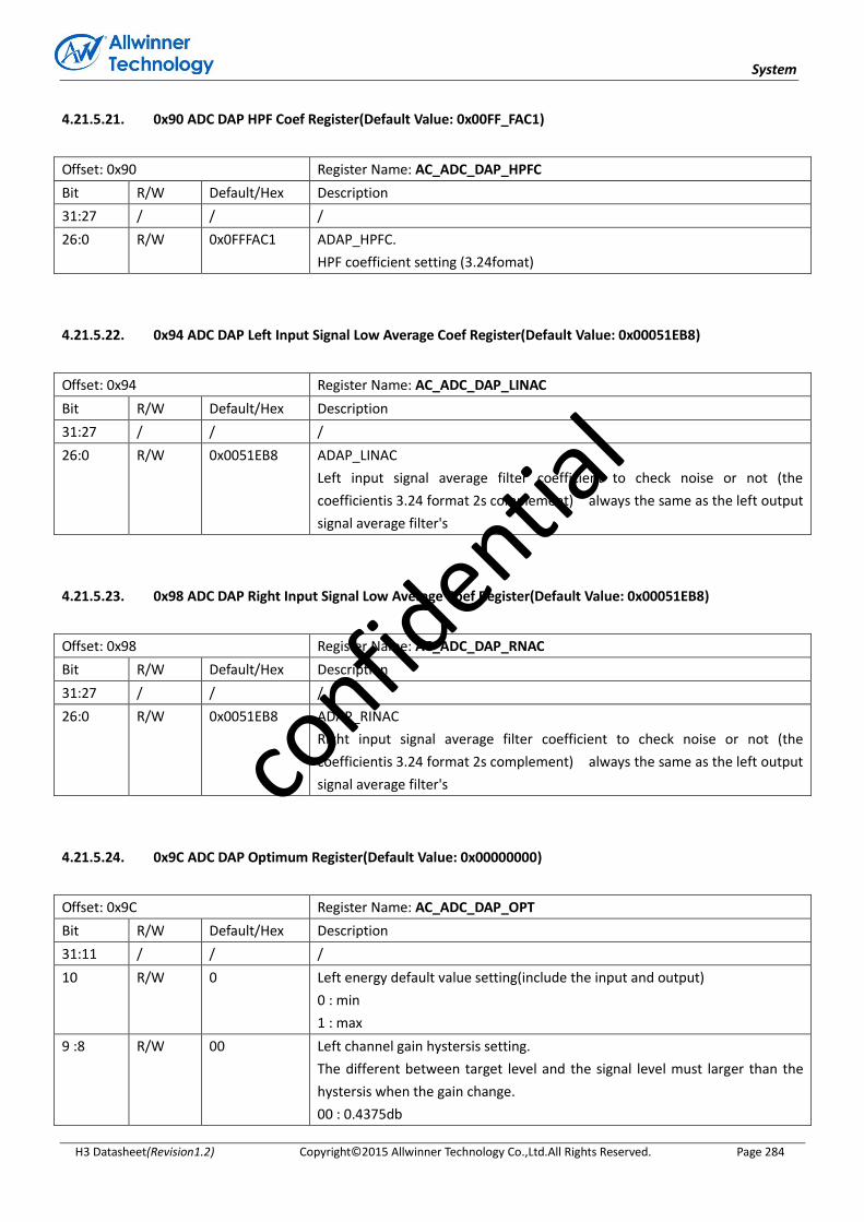
System
H3 Datasheet(Revision1.2) Copyright© 2015 Allwinner Technology Co.,Ltd.All Rights Reserved. Page 284
4.21.5.21. 0x90 ADC DAP HPF Coef Register(Default Value: 0x00FF_FAC1)
Offset: 0x90 Register Name: AC_ADC_DAP_HPFC
Bit R/W Default/Hex Description
31:27 / / /
26:0 R/W 0x0FFFAC1 ADAP_HPFC.
HPF coefficient setting (3.24fomat)
4.21.5.22. 0x94 ADC DAP Left Input Signal Low Average Coef Register(Default Value: 0x00051EB8)
Offset: 0x94 Register Name: AC_ADC_DAP_LINAC
Bit R/W Default/Hex Description
31:27 / / /
26:0 R/W 0x0051EB8 ADAP_LINAC
Left input signal average filter coefficient to check noise or not (the
coefficientis 3.24 format 2s complement) always the same as the left output
signal average filter's
4.21.5.23. 0x98 ADC DAP Right Input Signal Low Average Coef Register(Default Value: 0x00051EB8)
Offset: 0x98 Register Name: AC_ADC_DAP_RNAC
Bit R/W Default/Hex Description
31:27 / / /
26:0 R/W 0x0051EB8 ADAP_RINAC
Right input signal average filter coefficient to check noise or not (the
coefficientis 3.24 format 2s complement) always the same as the left output
signal average filter's
4.21.5.24. 0x9C ADC DAP Optimum Register(Default Value: 0x00000000)
Offset: 0x9C Register Name: AC_ADC_DAP_OPT
Bit R/W Default/Hex Description
31:11 / / /
10 R/W 0 Left energy default value setting(include the input and output)
0 : min
1 : max
9 :8 R/W 00 Left channel gain hystersis setting.
The different between target level and the signal level must larger than the
hystersis when the gain change.
00 : 0.4375db
confid
ential

System
H3 Datasheet(Revision1.2) Copyright© 2015 Allwinner Technology Co.,Ltd.All Rights Reserved. Page 285
01 : 0.9375db
10 : 1.9375db
11 : 3db
7:6 / / /
5 R/W 0 The input signal average filter coefficient setting
0 : is the reg94/reg98
1 : is the reg80/reg88;
4 R/W 0 AGC output when the channel in noise state
0 : output is zero
1 : output is the input data
3 / / /
2 R/W 0 Right energy default value setting(include the input and output)
0 : min
1 : max
1 :0 R/W 00 Right channel gain hysteresis setting.
The different between target level and the signal level must larger than the
hysteresis when the gain change.
00 : 0.4375db
01 : 0.9375db
10 : 1.9375db
11 : 3db
4.21.5.25. 0x100 DAC DRC High HPF Coef Register(Default Value: 0x000000FF)
Offset: 0x100 Register Name: AC_DAC_DRC_HHPFC
Bit R/W Default/Hex Description
15:11 / / /
10:0 R/W 0xff HPF coefficient setting and the data is 3.24 format.
4.21.5.26. 0x104 DAC DRC Low HPF Coef Register(Default Value: 0x0000FAC1)
Offset: 0x104 Register Name: AC_DAC_DRC_LHPFC
Bit R/W Default/Hex Description
15:0 R/W 0xFAC1 HPF coefficient setting and the data is 3.24 format.
4.21.5.27. 0x108 DAC DRC Control Register(Default Value: 0x00000080)
Offset: 0x108 Register Name: AC_DAC_DRC_CTRL
Bit R/W Default/Hex Description
15 R 0 DRC delay buffer data output state when drc delay function is enble and the
drc funciton disable. After disable drc function and this bit go to 0, the user
confid
ential

System
H3 Datasheet(Revision1.2) Copyright© 2015 Allwinner Technology Co.,Ltd.All Rights Reserved. Page 286
should write the drc delay function bit to 0;
0 : not complete
1 : is complete
14:10 / / /
13:8 R/W 0 Signal delay time setting
6'h00 : (8x1)fs
6'h01 : (8x2)fs
6'h02 : (8x3)fs
----------------------------------------
6'h2e : (8*47)fs
6'h2f : (8*48)fs
6'h30 -- 6'h3f : (8*48)fs
Delay time = 8*(n+1)fs, n<6'h30;
When the delay function is disable, the signal delay time is unused.
7 R/W 0x1 The delay buffer use or not when the drc disable and the drc buffer data
output completely
0 : don't use the buffer
1 : use the buffer
6 R/W 0x0 DRC gain max limit enable
0 : disable
1 : enable
5 R/W 0x0
DRC gain min limit enable. when this function enable, it will overwrite the
noise detect function.
0 : disable
1 : enable
4 R/W 0x0
Control the drc to detect noise when ET enable
0 : disable
1 : enable
3 R/W 0x0
Signal function Select
0 : RMS filter
1 : Peak filter
When Signal function Select Peak filter, the RMS parameter is unused.
(AC_DRC_LRMSHAT / AC_DRC_LRMSLAT / AC_DRC_LRMSHAT /
AC_DRC_LRMSLAT)
When Signal function Select RMS filter, the Peak filter parameter is
unused.(AC_DRC_LPFHAT / AC_DRC_LPFLAT / AC_DRC_RPFHAT /
AC_DRC_RPFLAT / AC_DRC_LPFHRT / AC_DRC_LPFLRT / AC_DRC_RPFHRT /
AC_DRC_RPFLRT)
2 R/W 0x0
Delay function enable
0 : disable
1 : enable
When the Delay function enable is disable, the Signal delay time is unused.
1 R/W 0x0
DRC LT enable
0 : disable
1 : enable
confid
ential

System
H3 Datasheet(Revision1.2) Copyright© 2015 Allwinner Technology Co.,Ltd.All Rights Reserved. Page 287
When the DRC LT is disable the LT, Kl and OPL parameter is unused.
0 R/W 0x0
DRC ET enable
0 : disable
1 : enable
When the DRC ET is disable the ET, Ke and OPE parameter is unused.
4.21.5.28. 0x10C DAC DRC Left Peak Filter High Attack Time Coef Register(Default Value: 0x0000_000B)
Offset: 0x10C Register Name: AC_DAC_DRC_LPFHAT
Bit R/W Default/Hex Description
15:11 / / /
10:0 R/W 0x000B The left peak filter attack time parameter setting, which determine by the
equation that AT = 1-exp(-2.2Ts/ta). The format is 3.24. (1ms)
4.21.5.29. 0x110 DAC DRC Left Peak Filter Low Attack Time Coef Register(Default Value: 0x000077BF)
Offset: 0x110 Register Name: AC_DAC_DRC_LPFLAT
Bit R/W Default/Hex Description
15:0 R/W 0x77BF The left peak filter attack time parameter setting, which determine by the
equation that AT = 1-exp(-2.2Ts/ta). The format is 3.24. (1ms)
4.21.5.30. 0x114 DAC DRC Right Peak Filter High Attack Time Coef Register(Default Value: 0x0000000B)
Offset: 0x114 Register Name: AC_DAC_DRC_RPFHAT
Bit R/W Default/Hex Description
15:11 / / /
10:0 R/W 0x000B The left peak filter attack time parameter setting, which determine by the
equation that AT = 1-exp(-2.2Ts/ta). The format is 3.24. (1ms)
4.21.5.31. 0x118 DAC DRC Peak Filter Low Attack Time Coef Register(Default Value: 0x000077BF)
Offset: 0x118 Register Name: AC_DAC_DRC_RPFLAT
Bit R/W Default/Hex Description
15:0 R/W 0x77BF The left peak filter attack time parameter setting, which determine by the
equation that AT = 1-exp(-2.2Ts/ta). The format is 3.24. (1ms)
confid
ential

System
H3 Datasheet(Revision1.2) Copyright© 2015 Allwinner Technology Co.,Ltd.All Rights Reserved. Page 288
4.21.5.32. 0x11C DAC DRC Left Peak Filter High Release Time Coef Register(Default Value: 0x000000FF)
Offset: 0x11C Register Name: AC_DAC_DRC_LPFHRT
Bit R/W Default/Hex Description
15:11 / / /
10:0 R/W 0x00FF The left peak filter release time parameter setting, which determine by the
equation that RT = exp(-2.2Ts/tr). The format is 3.24. (100ms)
4.21.5.33. 0x120 DAC DRC Left Peak Filter Low Release Time Coef Register(Default Value: 0x0000E1F8)
Offset: 0x120 Register Name: AC_DAC_DRC_LPFLRT
Bit R/W Default/Hex Description
15:0 R/W 0xE1F8 The left peak filter release time parameter setting, which determine by the
equation that RT = exp(-2.2Ts/tr). The format is 3.24. (100ms)
4.21.5.34. 0x124 DAC DRC Right Peak filter High Release Time Coef Register(Default Value: 0x0000_00FF)
Offset: 0x124 Register Name: AC_DAC_DRC_RPFHRT
Bit R/W Default/Hex Description
15:11 / / /
10:0 R/W 0x00FF The left peak filter attack time parameter setting, which determine by the
equation that RT = exp(-2.2Ts/tr). The format is 3.24. (100ms)
4.21.5.35. 0x128 DAC DRC Right Peak filter Low Release Time Coef Register(Default Value: 0x0000E1F8)
Offset: 0x128 Register Name: AC_DAC_DRC_RPFLRT
Bit R/W Default/Hex Description
15:0 R/W 0xE1F8 The left peak filter release time parameter setting, which determine by the
equation that AT = exp(-2.2Ts/tr). The format is 3.24. (100ms)
4.21.5.36. 0x12C DAC DRC Left RMS Filter High Coef Register(Default Value: 0x00000001)
Offset: 0x12C Register Name: AC_DAC_DRC_LRMSHAT
Bit R/W Default/Hex Description
15:11 / / /
10:0 R/W 0x0001 The left RMS filter average time parameter setting, which determine by the
equation that AT = 1-exp(-2.2Ts/tav). The format is 3.24. (10ms)
confid
ential

System
H3 Datasheet(Revision1.2) Copyright© 2015 Allwinner Technology Co.,Ltd.All Rights Reserved. Page 289
4.21.5.37. 0x130 DAC DRC Left RMS Filter Low Coef Register(Default Value: 0x00002BAF)
Offset: 0x130 Register Name: AC_DAC_DRC_LRMSLAT
Bit R/W Default/Hex Description
15:0 R/W 0x2BAF The left RMS filter average time parameter setting, which determine by the
equation that AT = 1-exp(-2.2Ts/tav). The format is 3.24. (10ms)
4.21.5.38. 0x134 DAC DRC Right RMS Filter High Coef Register(Default Value: 0x00000001)
Offset: 0x134 Register Name: AC_DAC_DRC_RRMSHAT
Bit R/W Default/Hex Description
15:11 / / /
10:0 R/W 0x0001 The right RMS filter average time parameter setting, which determine by the
equation that AT = 1-exp(-2.2Ts/tav). The format is 3.24. (10ms)
4.21.5.39. 0x138 DAC DRC Right RMS Filter Low Coef Register(Default Value: 0x00002BAF)
Offset: 0x138 Register Name: AC_DAC_DRC_RRMSLAT
Bit R/W Default/Hex Description
15:0 R/W 0x2BAF The right RMS filter average time parameter setting, which determine by the
equation that AT = 1-exp(-2.2Ts/tav). The format is 3.24. (10ms)
4.21.5.40. 0x13C DAC DRC Compressor Threshold High Setting Register(Default Value: 0x000006A4)
Offset: 0x13C Register Name: AC_DAC_DRC_HCT
Bit R/W Default/Hex Description
15:0 R/W 0x06A4 The compressor threshold setting, which set by the equation that CTin =
-CT/6.0206. The format is 8.24 (-40dB)
4.21.5.41. 0x140 DAC DRC Compressor Threshold High Setting Register(Default Value: 0x0000_D3C0)
Offset: 0x140 Register Name: AC_DAC_DRC_LCT
Bit R/W Default/Hex Description
15:0 R/W 0xD3C0 The compressor threshold setting, which set by the equation that CTin =
-CT/6.0206. The format is 8.24 (-40dB)
confid
ential
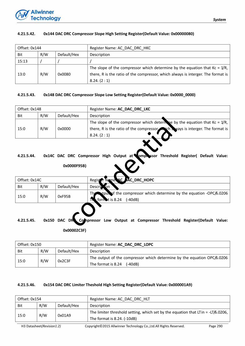
System
H3 Datasheet(Revision1.2) Copyright© 2015 Allwinner Technology Co.,Ltd.All Rights Reserved. Page 290
4.21.5.42. 0x144 DAC DRC Compressor Slope High Setting Register(Default Value: 0x00000080)
Offset: 0x144 Register Name: AC_DAC_DRC_HKC
Bit R/W Default/Hex Description
15:13 / / /
13:0 R/W 0x0080
The slope of the compressor which determine by the equation that Kc = 1/R,
there, R is the ratio of the compressor, which always is interger. The format is
8.24. (2 : 1)
4.21.5.43. 0x148 DAC DRC Compressor Slope Low Setting Register(Default Value: 0x0000_0000)
Offset: 0x148 Register Name: AC_DAC_DRC_LKC
Bit R/W Default/Hex Description
15:0 R/W 0x0000
The slope of the compressor which determine by the equation that Kc = 1/R,
there, R is the ratio of the compressor, which always is interger. The format is
8.24. (2 : 1)
4.21.5.44. 0x14C DAC DRC Compressor High Output at Compressor Threshold Register( Default Value:
0x0000F95B)
Offset: 0x14C Register Name: AC_DAC_DRC_HOPC
Bit R/W Default/Hex Description
15:0 R/W 0xF95B The output of the compressor which determine by the equation -OPC/6.0206
The format is 8.24 (-40dB)
4.21.5.45. 0x150 DAC DRC Compressor Low Output at Compressor Threshold Register(Default Value:
0x00002C3F)
Offset: 0x150 Register Name: AC_DAC_DRC_LOPC
Bit R/W Default/Hex Description
15:0 R/W 0x2C3F The output of the compressor which determine by the equation OPC/6.0206
The format is 8.24 (-40dB)
4.21.5.46. 0x154 DAC DRC Limiter Theshold High Setting Register(Default Value: 0x000001A9)
Offset: 0x154 Register Name: AC_DAC_DRC_HLT
Bit R/W Default/Hex Description
15:0 R/W 0x01A9 The limiter threshold setting, which set by the equation that LTin = -LT/6.0206,
The format is 8.24. (-10dB)
confid
ential

System
H3 Datasheet(Revision1.2) Copyright© 2015 Allwinner Technology Co.,Ltd.All Rights Reserved. Page 291
4.21.5.47. 0x158 DAC DRC Limiter Theshold Low Setting Register(Default Value: 0x0000_34F0)
Offset: 0x158 Register Name: AC_DAC_DRC_LLT
Bit R/W Default/Hex Description
15:0 R/W 0x34F0 The limiter threshold setting, which set by the equation that LTin = -LT/6.0206,
The format is 8.24. (-10dB)
4.21.5.48. 0x15C DAC DRC Limiter Slope High Setting Register(Default Value: 0x0000_0005)
Offset: 0x15C Register Name: AC_DAC_DRC_HKl
Bit R/W Default/Hex Description
15:11 / / /
13:0 R/W 0x0005 The slope of the limiter which determine by the equation that Kl = 1/R, there,
R is the ratio of the limiter, which always is interger. The format is 8.24. (50 :1)
4.21.5.49. 0x160 DAC DRC Limiter Slope Low Setting Register(Default Value: 0x00001EB8)
Offset: 0x160 Register Name: AC_DAC_DRC_LKl
Bit R/W Default/Hex Description
15:0 R/W 0x1EB8 The slope of the limiter which determine by the equation that Kl = 1/R, there,
R is the ratio of the limiter, which always is interger. The format is 8.24. (50 :1)
4.21.5.50. 0x164 DAC DRC Limiter High Output at Limiter Threshold(Default Value: 0x0000FBD8)
Offset: 0x164 Register Name: AC_DAC_DRC_HOPL
Bit R/W Default/Hex Description
15:0 R/W 0xFBD8 The output of the limiter which determine by equation OPT/6.0206. The
format is 8.24 (-25dB)
4.21.5.51. 0x168 DAC DRC Limiter Low Output at Limiter Threshold(Default Value: 0x0000FBA7)
Offset: 0x168 Register Name: AC_DAC_DRC_LOPL
Bit R/W Default/Hex Description
15:0 R/W 0xFBA7 The output of the limiter which determine by equation OPT/6.0206. The
format is 8.24 (-25dB)
confid
ential

System
H3 Datasheet(Revision1.2) Copyright© 2015 Allwinner Technology Co.,Ltd.All Rights Reserved. Page 292
4.21.5.52. 0x16C DAC DRC Expander Theshold High Setting Register(Default Value: 0x00000BA0)
Offset: 0x16C Register Name: AC_DAC_DRC_HET
Bit R/W Default/Hex Description
15:0 R/W 0x0BA0 The expander threshold setting, which set by the equation that ETin =
-ET/6.0206, The format is 8.24. (-70dB)
4.21.5.53. 0x170 DAC DRC Expander Theshold Low Setting Register(Default Value: 0x00007291)
Offset: 0x170 Register Name: AC_DAC_DRC_LET
Bit R/W Default/Hex Description
15:0 R/W 0x7291 The expander threshold setting, which set by the equation that ETin =
-ET/6.0206, The format is 8.24. (-70dB)
4.21.5.54. 0x174 DAC DRC Expander Slope High Setting Register(Default Value: 0x00000500)
Offset: 0x174 Register Name: AC_DAC_DRC_HKE
Bit R/W Default/Hex Description
15:14 / / /
13:0 R/W 0x0500
The slope of the expander which determine by the equation that Ke = 1/R,
there, R is the ratio of the expander, which always is interger and the ke must
larger than 50. The format is 8.24. (1:5)
4.21.5.55. 0x178 DAC DRC Expander Slope Low Setting Register(Default Value: 0x00000000)
Offset: 0x178 Register Name: AC_DAC_DRC_LKE
Bit R/W Default/Hex Description
15:0 R/W 0x0000
The slope of the expander which determine by the equation that Ke = 1/R,
there, R is the ratio of the expander, which always is interger and the ke must
larger than 50. The format is 8.24. (1:5)
4.21.5.56. 0x17C DAC DRC Expander High Output at Expander Threshold(Default Value: 0x0000F45F)
Offset: 0x17C Register Name: AC_DAC_DRC_HOPE
Bit R/W Default/Hex Description
15:0 R/W 0xF45F The output of the expander which determine by equation OPE/6.0206. The
format is 8.24 (-70dB)
confid
ential

System
H3 Datasheet(Revision1.2) Copyright© 2015 Allwinner Technology Co.,Ltd.All Rights Reserved. Page 293
4.21.5.57. 0x180 DAC DRC Expander Low Output at Expander Threshold(Default Value: 0x00008D6E)
Offset: 0x180 Register Name: AC_DAC_DRC_LOPE
Bit R/W Default/Hex Description
15:0 R/W 0x8D6E The output of the expander which determine by equation OPE/6.0206. The
format is 8.24 (-70dB)
4.21.5.58. 0x184 DAC DRC Linear Slope High Setting Register(Default Value: 0x00000100)
Offset: 0x184 Register Name: AC_DAC_DRC_HKN
Bit R/W Default/Hex Description
15:14 / / /
13:0 R/W 0x0100 The slope of the linear which determine by the equation that Kn = 1/R, there,
R is the ratio of the linear, which always is interger . The format is 8.24. (1:1)
4.21.5.59. 0x188 DAC DRC Linear Slope Low Setting Register(Default Value: 0x00000000)
Offset: 0x188 Register Name: AC_DAC_DRC_LKN
Bit R/W Default/Hex Description
15:0 R/W 0x0000 The slope of the linear which determine by the equation that Kn = 1/R, there,
R is the ratio of the linear, which always is interger . The format is 8.24. (1:1)
4.21.5.60. 0x18C DAC DRC Smooth filter Gain High Attack Time Coef Register(Default Value: 0x00000002)
Offset: 0x18C Register Name: AC_DAC_DRC_SFHAT
Bit R/W Default/Hex Description
15:11 / / /
10:0 R/W 0x0002 The smooth filter attack time parameter setting, which determine by the
equation that AT = 1-exp(-2.2Ts/tr). The format is 3.24. (5ms)
4.21.5.61. 0x190 DAC DRC Smooth filter Gain Low Attack Time Coef Register(Default Value: 0x00005600)
Offset: 0x190 Register Name: AC_DAC_DRC_SFLAT
Bit R/W Default/Hex Description
15:0 R/W 0x5600 The smooth filter attack time parameter setting, which determine by the
equation that AT = 1-exp(-2.2Ts/tr). The format is 3.24. (5ms)
confid
ential
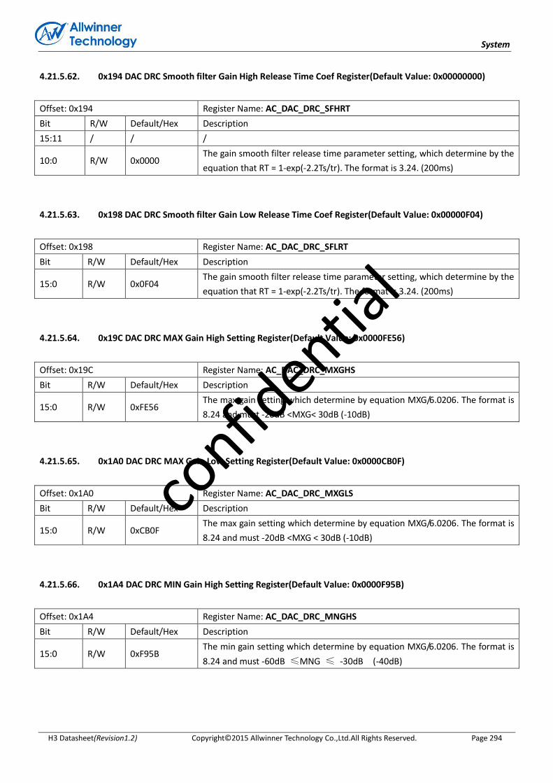
System
H3 Datasheet(Revision1.2) Copyright© 2015 Allwinner Technology Co.,Ltd.All Rights Reserved. Page 294
4.21.5.62. 0x194 DAC DRC Smooth filter Gain High Release Time Coef Register(Default Value: 0x00000000)
Offset: 0x194 Register Name: AC_DAC_DRC_SFHRT
Bit R/W Default/Hex Description
15:11 / / /
10:0 R/W 0x0000 The gain smooth filter release time parameter setting, which determine by the
equation that RT = 1-exp(-2.2Ts/tr). The format is 3.24. (200ms)
4.21.5.63. 0x198 DAC DRC Smooth filter Gain Low Release Time Coef Register(Default Value: 0x00000F04)
Offset: 0x198 Register Name: AC_DAC_DRC_SFLRT
Bit R/W Default/Hex Description
15:0 R/W 0x0F04 The gain smooth filter release time parameter setting, which determine by the
equation that RT = 1-exp(-2.2Ts/tr). The format is 3.24. (200ms)
4.21.5.64. 0x19C DAC DRC MAX Gain High Setting Register(Default Value: 0x0000FE56)
Offset: 0x19C Register Name: AC_DAC_DRC_MXGHS
Bit R/W Default/Hex Description
15:0 R/W 0xFE56 The max gain setting which determine by equation MXG/6.0206. The format is
8.24 and must -20dB <MXG< 30dB (-10dB)
4.21.5.65. 0x1A0 DAC DRC MAX Gain Low Setting Register(Default Value: 0x0000CB0F)
Offset: 0x1A0 Register Name: AC_DAC_DRC_MXGLS
Bit R/W Default/Hex Description
15:0 R/W 0xCB0F The max gain setting which determine by equation MXG/6.0206. The format is
8.24 and must -20dB <MXG < 30dB (-10dB)
4.21.5.66. 0x1A4 DAC DRC MIN Gain High Setting Register(Default Value: 0x0000F95B)
Offset: 0x1A4 Register Name: AC_DAC_DRC_MNGHS
Bit R/W Default/Hex Description
15:0 R/W 0xF95B The min gain setting which determine by equation MXG/6.0206. The format is
8.24 and must -60dB ≤MNG ≤ -30dB (-40dB)
confid
ential
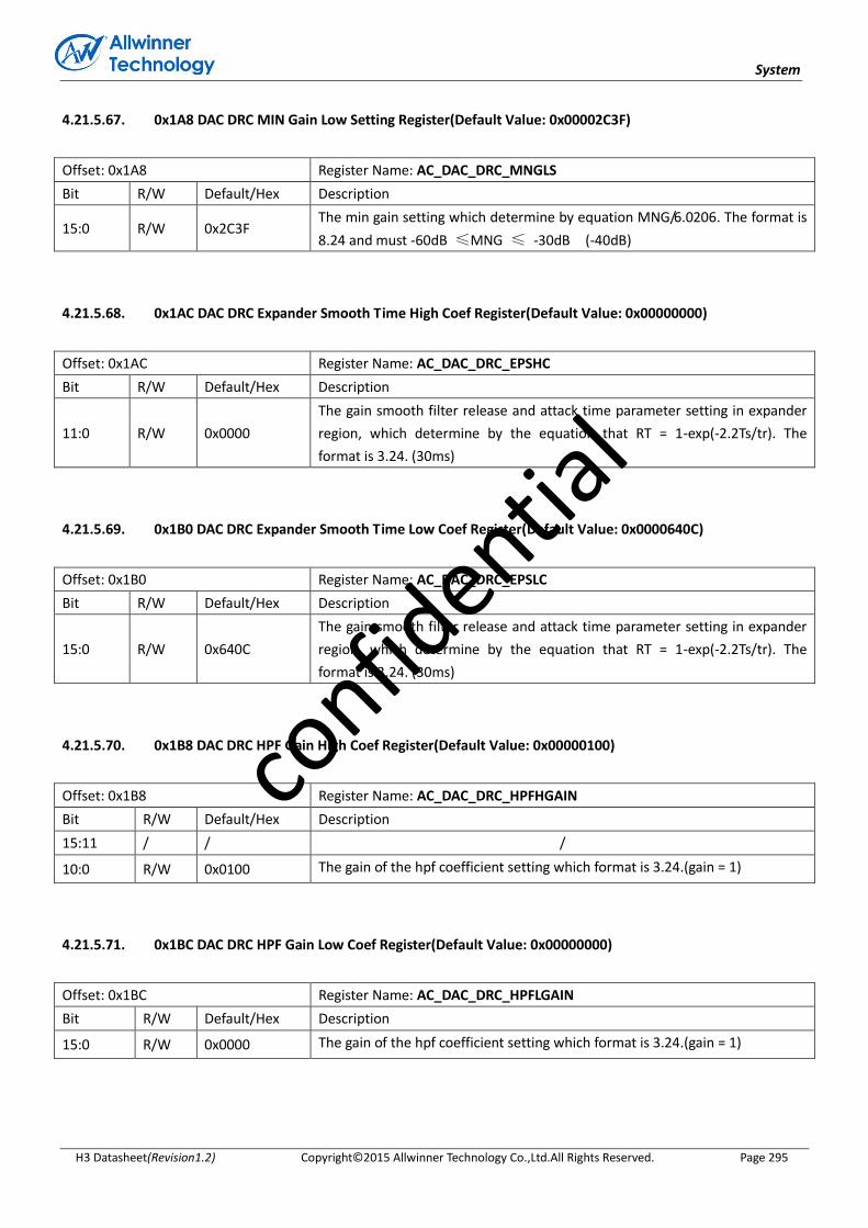
System
H3 Datasheet(Revision1.2) Copyright© 2015 Allwinner Technology Co.,Ltd.All Rights Reserved. Page 295
4.21.5.67. 0x1A8 DAC DRC MIN Gain Low Setting Register(Default Value: 0x00002C3F)
Offset: 0x1A8 Register Name: AC_DAC_DRC_MNGLS
Bit R/W Default/Hex Description
15:0 R/W 0x2C3F The min gain setting which determine by equation MNG/6.0206. The format is
8.24 and must -60dB ≤MNG ≤ -30dB (-40dB)
4.21.5.68. 0x1AC DAC DRC Expander Smooth Time High Coef Register(Default Value: 0x00000000)
Offset: 0x1AC Register Name: AC_DAC_DRC_EPSHC
Bit R/W Default/Hex Description
11:0 R/W 0x0000
The gain smooth filter release and attack time parameter setting in expander
region, which determine by the equation that RT = 1-exp(-2.2Ts/tr). The
format is 3.24. (30ms)
4.21.5.69. 0x1B0 DAC DRC Expander Smooth Time Low Coef Register(Default Value: 0x0000640C)
Offset: 0x1B0 Register Name: AC_DAC_DRC_EPSLC
Bit R/W Default/Hex Description
15:0 R/W 0x640C
The gain smooth filter release and attack time parameter setting in expander
region, which determine by the equation that RT = 1-exp(-2.2Ts/tr). The
format is 3.24. (30ms)
4.21.5.70. 0x1B8 DAC DRC HPF Gain High Coef Register(Default Value: 0x00000100)
Offset: 0x1B8 Register Name: AC_DAC_DRC_HPFHGAIN
Bit R/W Default/Hex Description
15:11 / / /
10:0 R/W 0x0100 The gain of the hpf coefficient setting which format is 3.24.(gain = 1)
4.21.5.71. 0x1BC DAC DRC HPF Gain Low Coef Register(Default Value: 0x00000000)
Offset: 0x1BC Register Name: AC_DAC_DRC_HPFLGAIN
Bit R/W Default/Hex Description
15:0 R/W 0x0000 The gain of the hpf coefficient setting which format is 3.24.(gain = 1)
confid
ential

System
H3 Datasheet(Revision1.2) Copyright© 2015 Allwinner Technology Co.,Ltd.All Rights Reserved. Page 296
4.21.5.72. 0x200 ADC DRC High HPF Coef Register(Default Value: 0x000000FF)
Offset: 0x200 Register Name: AC_ADC_DRC_HHPFC
Bit R/W Default/Hex Description
15:11 / / /
10:0 R/W 0xFF HPF coefficient setting and the data is 3.24 format.
4.21.5.73. 0x204 ADC DRC Low HPF Coef Register(Default Value: 0x0000FAC1)
Offset: 0x204 Register Name: AC_ADC_DRC_LHPFC
Bit R/W Default/Hex Description
15:0 R/W 0xFAC1 HPF coefficient setting and the data is 3.24 format.
4.21.5.74. 0x208 ADC DRC Control Register(Default Value: 0x00000080)
Offset: 0x208 Register Name: AC_ADC_DRC_CTRL
Bit R/W Default/Hex Description
15 R 0 DRC delay buffer data output state when drc delay function is enable and the
drc function disable. After disable drc function and this bit go to 0, the user
should write the drc delay function bit to 0;
0 : not complete
1 : is complete
14:10 / / /
13:8 R/W 0 Signal delay time setting
6'h00 : (8x1)fs
6'h01 : (8x2)fs
6'h02 : (8x3)fs
----------------------------------------
6'h2e : (8*47)fs
6'h2f : (8*48)fs
6'h30 -- 6'h3f : (8*48)fs
Delay time = 8*(n+1)fs, n<6'h30;
When the delay function is disable, the signal delay time is unused.
7 R/W 0x1 The delay buffer use or not when the drc disable and the drc buffer data output
completely
0 : don't use the buffer
1 : use the buffer
6 R/W 0x0 DRC gain max limit enable
0 : disable
1 : enable
5 R/W 0x0 DRC gain min limit enable. when this function enable, it will overwrite the noise
detect function.
confid
ential
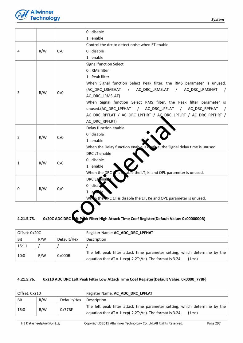
System
H3 Datasheet(Revision1.2) Copyright© 2015 Allwinner Technology Co.,Ltd.All Rights Reserved. Page 297
0 : disable
1 : enable
4 R/W 0x0
Control the drc to detect noise when ET enable
0 : disable
1 : enable
3 R/W 0x0
Signal function Select
0 : RMS filter
1 : Peak filter
When Signal function Select Peak filter, the RMS parameter is unused.
(AC_DRC_LRMSHAT / AC_DRC_LRMSLAT / AC_DRC_LRMSHAT /
AC_DRC_LRMSLAT)
When Signal function Select RMS filter, the Peak filter parameter is
unused.(AC_DRC_LPFHAT / AC_DRC_LPFLAT / AC_DRC_RPFHAT /
AC_DRC_RPFLAT / AC_DRC_LPFHRT / AC_DRC_LPFLRT / AC_DRC_RPFHRT /
AC_DRC_RPFLRT)
2 R/W 0x0
Delay function enable
0 : disable
1 : enable
When the Delay function enable is disable, the Signal delay time is unused.
1 R/W 0x0
DRC LT enable
0 : disable
1 : enable
When the DRC LT is disable the LT, Kl and OPL parameter is unused.
0 R/W 0x0
DRC ET enable
0 : disable
1 : enable
When the DRC ET is disable the ET, Ke and OPE parameter is unused.
4.21.5.75. 0x20C ADC DRC Left Peak Filter High Attack Time Coef Register(Default Value: 0x0000000B)
Offset: 0x20C Register Name: AC_ADC_DRC_LPFHAT
Bit R/W Default/Hex Description
15:11 / / /
10:0 R/W 0x000B The left peak filter attack time parameter setting, which determine by the
equation that AT = 1-exp(-2.2Ts/ta). The format is 3.24. (1ms)
4.21.5.76. 0x210 ADC DRC Left Peak Filter Low Attack Time Coef Register(Default Value: 0x0000_77BF)
Offset: 0x210 Register Name: AC_ADC_DRC_LPFLAT
Bit R/W Default/Hex Description
15:0 R/W 0x77BF The left peak filter attack time parameter setting, which determine by the
equation that AT = 1-exp(-2.2Ts/ta). The format is 3.24. (1ms)
confid
ential
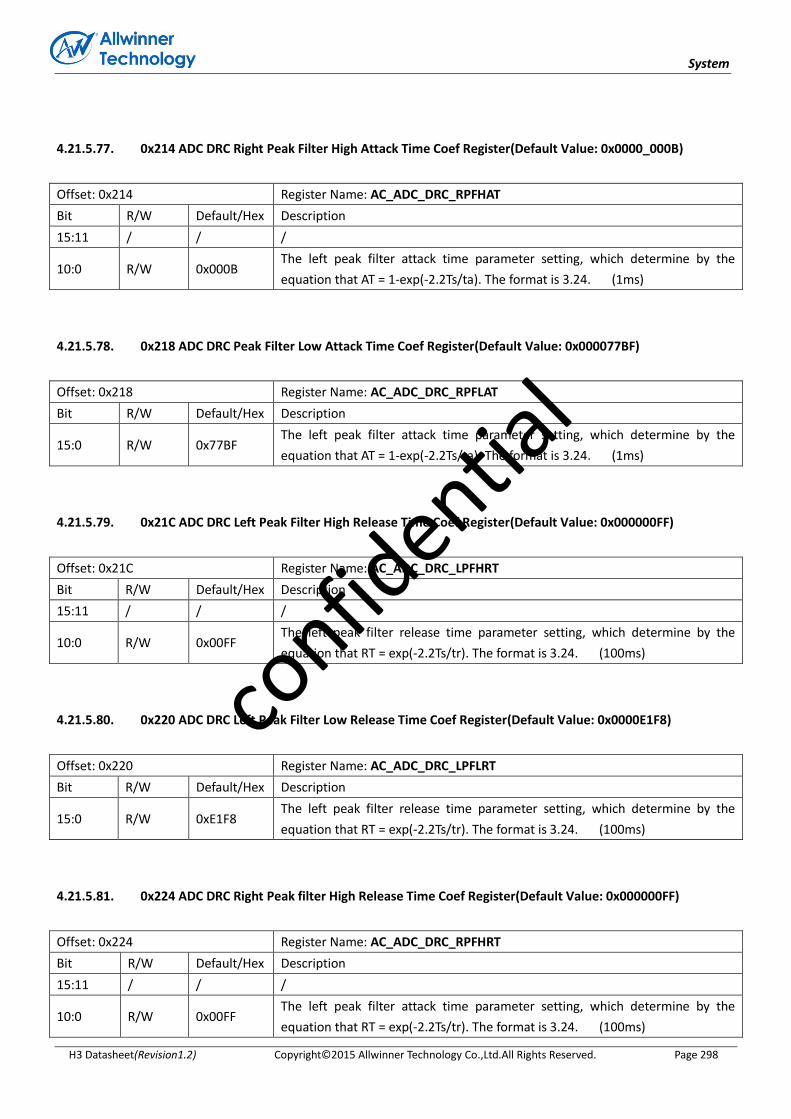
System
H3 Datasheet(Revision1.2) Copyright© 2015 Allwinner Technology Co.,Ltd.All Rights Reserved. Page 298
4.21.5.77. 0x214 ADC DRC Right Peak Filter High Attack Time Coef Register(Default Value: 0x0000_000B)
Offset: 0x214 Register Name: AC_ADC_DRC_RPFHAT
Bit R/W Default/Hex Description
15:11 / / /
10:0 R/W 0x000B The left peak filter attack time parameter setting, which determine by the
equation that AT = 1-exp(-2.2Ts/ta). The format is 3.24. (1ms)
4.21.5.78. 0x218 ADC DRC Peak Filter Low Attack Time Coef Register(Default Value: 0x000077BF)
Offset: 0x218 Register Name: AC_ADC_DRC_RPFLAT
Bit R/W Default/Hex Description
15:0 R/W 0x77BF The left peak filter attack time parameter setting, which determine by the
equation that AT = 1-exp(-2.2Ts/ta). The format is 3.24. (1ms)
4.21.5.79. 0x21C ADC DRC Left Peak Filter High Release Time Coef Register(Default Value: 0x000000FF)
Offset: 0x21C Register Name: AC_ADC_DRC_LPFHRT
Bit R/W Default/Hex Description
15:11 / / /
10:0 R/W 0x00FF The left peak filter release time parameter setting, which determine by the
equation that RT = exp(-2.2Ts/tr). The format is 3.24. (100ms)
4.21.5.80. 0x220 ADC DRC Left Peak Filter Low Release Time Coef Register(Default Value: 0x0000E1F8)
Offset: 0x220 Register Name: AC_ADC_DRC_LPFLRT
Bit R/W Default/Hex Description
15:0 R/W 0xE1F8 The left peak filter release time parameter setting, which determine by the
equation that RT = exp(-2.2Ts/tr). The format is 3.24. (100ms)
4.21.5.81. 0x224 ADC DRC Right Peak filter High Release Time Coef Register(Default Value: 0x000000FF)
Offset: 0x224 Register Name: AC_ADC_DRC_RPFHRT
Bit R/W Default/Hex Description
15:11 / / /
10:0 R/W 0x00FF The left peak filter attack time parameter setting, which determine by the
equation that RT = exp(-2.2Ts/tr). The format is 3.24. (100ms)
confid
ential
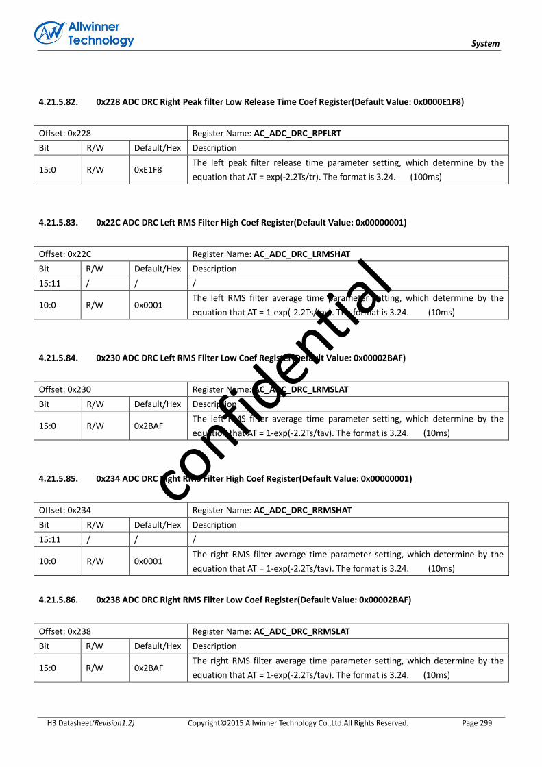
System
H3 Datasheet(Revision1.2) Copyright© 2015 Allwinner Technology Co.,Ltd.All Rights Reserved. Page 299
4.21.5.82. 0x228 ADC DRC Right Peak filter Low Release Time Coef Register(Default Value: 0x0000E1F8)
Offset: 0x228 Register Name: AC_ADC_DRC_RPFLRT
Bit R/W Default/Hex Description
15:0 R/W 0xE1F8 The left peak filter release time parameter setting, which determine by the
equation that AT = exp(-2.2Ts/tr). The format is 3.24. (100ms)
4.21.5.83. 0x22C ADC DRC Left RMS Filter High Coef Register(Default Value: 0x00000001)
Offset: 0x22C Register Name: AC_ADC_DRC_LRMSHAT
Bit R/W Default/Hex Description
15:11 / / /
10:0 R/W 0x0001 The left RMS filter average time parameter setting, which determine by the
equation that AT = 1-exp(-2.2Ts/tav). The format is 3.24. (10ms)
4.21.5.84. 0x230 ADC DRC Left RMS Filter Low Coef Register(Default Value: 0x00002BAF)
Offset: 0x230 Register Name: AC_ADC_DRC_LRMSLAT
Bit R/W Default/Hex Description
15:0 R/W 0x2BAF The left RMS filter average time parameter setting, which determine by the
equation that AT = 1-exp(-2.2Ts/tav). The format is 3.24. (10ms)
4.21.5.85. 0x234 ADC DRC Right RMS Filter High Coef Register(Default Value: 0x00000001)
Offset: 0x234 Register Name: AC_ADC_DRC_RRMSHAT
Bit R/W Default/Hex Description
15:11 / / /
10:0 R/W 0x0001 The right RMS filter average time parameter setting, which determine by the
equation that AT = 1-exp(-2.2Ts/tav). The format is 3.24. (10ms)
4.21.5.86. 0x238 ADC DRC Right RMS Filter Low Coef Register(Default Value: 0x00002BAF)
Offset: 0x238 Register Name: AC_ADC_DRC_RRMSLAT
Bit R/W Default/Hex Description
15:0 R/W 0x2BAF The right RMS filter average time parameter setting, which determine by the
equation that AT = 1-exp(-2.2Ts/tav). The format is 3.24. (10ms)
confid
ential
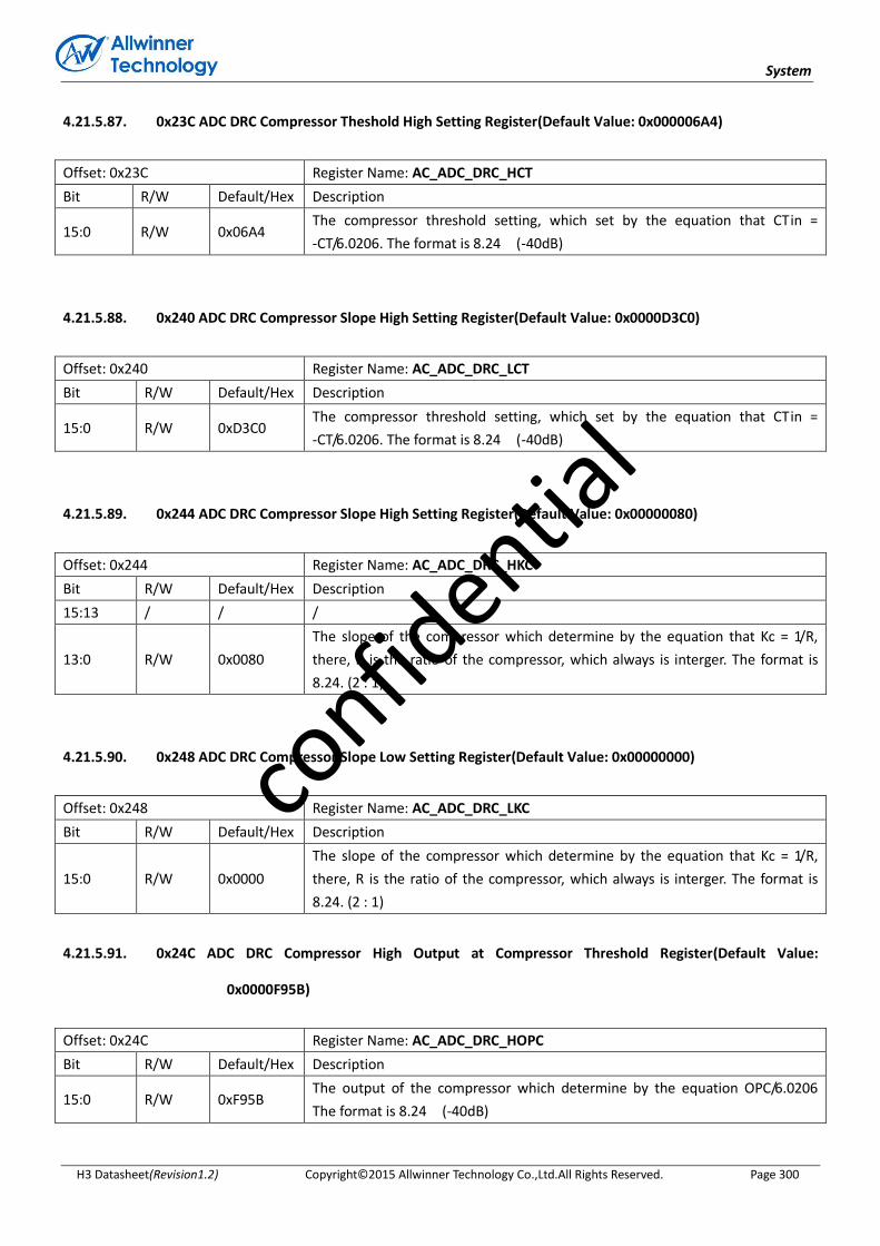
System
H3 Datasheet(Revision1.2) Copyright© 2015 Allwinner Technology Co.,Ltd.All Rights Reserved. Page 300
4.21.5.87. 0x23C ADC DRC Compressor Theshold High Setting Register(Default Value: 0x000006A4)
Offset: 0x23C Register Name: AC_ADC_DRC_HCT
Bit R/W Default/Hex Description
15:0 R/W 0x06A4 The compressor threshold setting, which set by the equation that CTin =
-CT/6.0206. The format is 8.24 (-40dB)
4.21.5.88. 0x240 ADC DRC Compressor Slope High Setting Register(Default Value: 0x0000D3C0)
Offset: 0x240 Register Name: AC_ADC_DRC_LCT
Bit R/W Default/Hex Description
15:0 R/W 0xD3C0 The compressor threshold setting, which set by the equation that CTin =
-CT/6.0206. The format is 8.24 (-40dB)
4.21.5.89. 0x244 ADC DRC Compressor Slope High Setting Register(Default Value: 0x00000080)
Offset: 0x244 Register Name: AC_ADC_DRC_HKC
Bit R/W Default/Hex Description
15:13 / / /
13:0 R/W 0x0080
The slope of the compressor which determine by the equation that Kc = 1/R,
there, R is the ratio of the compressor, which always is interger. The format is
8.24. (2 : 1)
4.21.5.90. 0x248 ADC DRC Compressor Slope Low Setting Register(Default Value: 0x00000000)
Offset: 0x248 Register Name: AC_ADC_DRC_LKC
Bit R/W Default/Hex Description
15:0 R/W 0x0000
The slope of the compressor which determine by the equation that Kc = 1/R,
there, R is the ratio of the compressor, which always is interger. The format is
8.24. (2 : 1)
4.21.5.91. 0x24C ADC DRC Compressor High Output at Compressor Threshold Register(Default Value:
0x0000F95B)
Offset: 0x24C Register Name: AC_ADC_DRC_HOPC
Bit R/W Default/Hex Description
15:0 R/W 0xF95B The output of the compressor which determine by the equation OPC/6.0206
The format is 8.24 (-40dB)
confid
ential

System
H3 Datasheet(Revision1.2) Copyright© 2015 Allwinner Technology Co.,Ltd.All Rights Reserved. Page 301
4.21.5.92. 0x250 ADC DRC Compressor Low Output at Compressor Threshold Register(Default Value:
0x00002C3F)
Offset: 0x250 Register Name: AC_ADC_DRC_LOPC
Bit R/W Default/Hex Description
15:0 R/W 0x2C3F The output of the compressor which determine by the equation OPC/6.0206
The format is 8.24 (-40dB)
4.21.5.93. 0x254 ADC DRC Limiter Theshold High Setting Register(Default Value: 0x000001A9)
Offset: 0x254 Register Name: AC_ADC_DRC_HLT
Bit R/W Default/Hex Description
15:0 R/W 0x01A9 The limiter threshold setting, which set by the equation that LTin = -LT/6.0206,
The format is 8.24. (-10dB)
4.21.5.94. 0x258 ADC DRC Limiter Theshold Low Setting Register(Default Value: 0x000034F0)
Offset: 0x258 Register Name: AC_ADC_DRC_LLT
Bit R/W Default/Hex Description
15:0 R/W 0x34F0 The limiter threshold setting, which set by the equation that LTin = -LT/6.0206,
The format is 8.24. (-10dB)
4.21.5.95. 0x25C ADC DRC Limiter Slope High Setting Register(Default Value: 0x00000005)
Offset: 0x25C Register Name: AC_ADC_DRC_HKl
Bit R/W Default/Hex Description
15:11 / / /
13:0 R/W 0x0005 The slope of the limiter which determine by the equation that Kl = 1/R, there, R
is the ratio of the limiter, which always is interger. The format is 8.24. (50 :1)
4.21.5.96. 0x260 ADC DRC Limiter Slope Low Setting Register(Default Value: 0x1EB8)
Offset: 0x260 Register Name: AC_ADC_DRC_LKl
Bit R/W Default/Hex Description
15:0 R/W 0x1EB8 The slope of the limiter which determine by the equation that Kl = 1/R, there, R
is the ratio of the limiter, which always is interger. The format is 8.24. (50 :1)
confid
ential

System
H3 Datasheet(Revision1.2) Copyright© 2015 Allwinner Technology Co.,Ltd.All Rights Reserved. Page 302
4.21.5.97. 0x264 ADC DRC Limiter High Output at Limiter Threshold(Default Value: 0x0000FBD8)
Offset: 0x264 Register Name: AC_ADC_DRC_HOPL
Bit R/W Default/Hex Description
15:0 R/W 0xFBD8 The output of the limiter which determine by equation OPT/6.0206. The format
is 8.24 (-25dB)
4.21.5.98. 0x268 ADC DRC Limiter Low Output at Limiter Threshold(Default Value: 0x0000FBA7)
Offset: 0x268 Register Name: AC_ADC_DRC_LOPL
Bit R/W Default/Hex Description
15:0 R/W 0xFBA7 The output of the limiter which determine by equation OPT/6.0206. The format
is 8.24 (-25dB)
4.21.5.99. 0x26C ADC DRC Expander Theshold High Setting Register(Default Value: 0x00000BA0)
Offset: 0x26C Register Name: AC_ADC_DRC_HET
Bit R/W Default/Hex Description
15:0 R/W 0x0BA0 The expander threshold setting, which set by the equation that ETin =
-ET/6.0206, The format is 8.24. (-70dB)
4.21.5.100. 0x270 ADC DRC Expander Theshold Low Setting Register(Default Value: 0x00007291)
Offset: 0x270 Register Name: AC_ADC_DRC_LET
Bit R/W Default/Hex Description
15:0 R/W 0x7291 The expander threshold setting, which set by the equation that ETin =
-ET/6.0206, The format is 8.24. (-70dB)
4.21.5.101. 0x274 ADC DRC Expander Slope High Setting Register(Default Value: 0x00000500)
Offset: 0x274 Register Name: AC_ADC_DRC_HKE
Bit R/W Default/Hex Description
15:14 / / /
13:0 R/W 0x0500
The slope of the expander which determine by the equation that Ke = 1/R,
there, R is the ratio of the expander, which always is interger and the ke must
larger than 50. The format is 8.24. (1:5)
confid
ential

System
H3 Datasheet(Revision1.2) Copyright© 2015 Allwinner Technology Co.,Ltd.All Rights Reserved. Page 303
4.21.5.102. 0x278 ADC DRC Expander Slope Low Setting Register(Default Value: 0x00000000)
Offset: 0x278 Register Name: AC_ADC_DRC_LKE
Bit R/W Default/Hex Description
15:0 R/W 0x0000
The slope of the expander which determine by the equation that Ke = 1/R,
there, R is the ratio of the expander, which always is interger and the ke must
larger than 50. The format is 8.24. (1:5)
4.21.5.103. 0x27C ADC DRC Expander High Output at Expander Threshold(Default Value: 0x0000F45F)
Offset: 0x27C Register Name: AC_ADC_DRC_HOPE
Bit R/W Default/Hex Description
15:0 R/W 0xF45F The output of the expander which determine by equation OPE/6.0206. The
format is 8.24 (-70dB)
4.21.5.104. 0x280 ADC DRC Expander Low Output at Expander Threshold(Default Value: 0x00008D6E)
Offset: 0x280 Register Name: AC_ADC_DRC_LOPE
Bit R/W Default/Hex Description
15:0 R/W 0x8D6E The output of the expander which determine by equation OPE/6.0206. The
format is 8.24 (-70dB)
4.21.5.105. 0x284 ADC DRC Linear Slope High Setting Register(Default Value: 0x00000100)
Offset: 0x284 Register Name: AC_ADC_DRC_HKN
Bit R/W Default/Hex Description
15:14 / / /
13:0 R/W 0x0100 The slope of the linear which determine by the equation that Kn = 1/R, there, R
is the ratio of the linear, which always is interger . The format is 8.24. (1:1)
4.21.5.106. 0x288 ADC DRC Linear Slope Low Setting Register(Default Value: 0x00000000)
Offset: 0x288 Register Name: AC_ADC_DRC_LKN
Bit R/W Default/Hex Description
15:0 R/W 0x0000 The slope of the linear which determine by the equation that Kn = 1/R, there, R
is the ratio of the linear, which always is interger . The format is 8.24. (1:1)
confid
ential
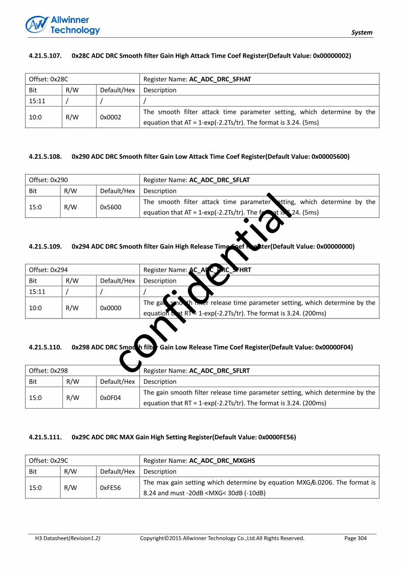
System
H3 Datasheet(Revision1.2) Copyright© 2015 Allwinner Technology Co.,Ltd.All Rights Reserved. Page 304
4.21.5.107. 0x28C ADC DRC Smooth filter Gain High Attack Time Coef Register(Default Value: 0x00000002)
Offset: 0x28C Register Name: AC_ADC_DRC_SFHAT
Bit R/W Default/Hex Description
15:11 / / /
10:0 R/W 0x0002 The smooth filter attack time parameter setting, which determine by the
equation that AT = 1-exp(-2.2Ts/tr). The format is 3.24. (5ms)
4.21.5.108. 0x290 ADC DRC Smooth filter Gain Low Attack Time Coef Register(Default Value: 0x00005600)
Offset: 0x290 Register Name: AC_ADC_DRC_SFLAT
Bit R/W Default/Hex Description
15:0 R/W 0x5600 The smooth filter attack time parameter setting, which determine by the
equation that AT = 1-exp(-2.2Ts/tr). The format is 3.24. (5ms)
4.21.5.109. 0x294 ADC DRC Smooth filter Gain High Release Time Coef Register(Default Value: 0x00000000)
Offset: 0x294 Register Name: AC_ADC_DRC_SFHRT
Bit R/W Default/Hex Description
15:11 / / /
10:0 R/W 0x0000 The gain smooth filter release time parameter setting, which determine by the
equation that RT = 1-exp(-2.2Ts/tr). The format is 3.24. (200ms)
4.21.5.110. 0x298 ADC DRC Smooth filter Gain Low Release Time Coef Register(Default Value: 0x00000F04)
Offset: 0x298 Register Name: AC_ADC_DRC_SFLRT
Bit R/W Default/Hex Description
15:0 R/W 0x0F04 The gain smooth filter release time parameter setting, which determine by the
equation that RT = 1-exp(-2.2Ts/tr). The format is 3.24. (200ms)
4.21.5.111. 0x29C ADC DRC MAX Gain High Setting Register(Default Value: 0x0000FE56)
Offset: 0x29C Register Name: AC_ADC_DRC_MXGHS
Bit R/W Default/Hex Description
15:0 R/W 0xFE56 The max gain setting which determine by equation MXG/6.0206. The format is
8.24 and must -20dB <MXG< 30dB (-10dB)
confid
ential

System
H3 Datasheet(Revision1.2) Copyright© 2015 Allwinner Technology Co.,Ltd.All Rights Reserved. Page 305
4.21.5.112. 0x2A0 ADC DRC MAX Gain Low Setting Register(Default Value: 0x0000CB0F)
Offset: 0x2A0 Register Name: AC_ADC_DRC_MXGLS
Bit R/W Default/Hex Description
15:0 R/W 0xCB0F The max gain setting which determine by equation MXG/6.0206. The format is
8.24 and must -20dB <MXG < 30dB (-10dB)
4.21.5.113. 0x2A4 ADC DRC MIN Gain High Setting Register(Default Value: 0x0000F95B)
Offset: 0x2A4 Register Name: AC_ADC_DRC_MNGHS
Bit R/W Default/Hex Description
15:0 R/W 0xF95B The min gain setting which determine by equation MXG/6.0206. The format is
8.24 and must -60dB ≤MNG ≤ -30dB (-40dB)
4.21.5.114. 0x2A8 ADC DRC MIN Gain Low Setting Register(Default Value: 0x00002C3F)
Offset: 0x2A8 Register Name: AC_ADC_DRC_MNGLS
Bit R/W Default/Hex Description
15:0 R/W 0x2C3F The min gain setting which determine by equation MNG/6.0206. The format is
8.24 and must -60dB ≤MNG ≤ -30dB (-40dB)
4.21.5.115. 0x2AC ADC DRC Expander Smooth Time High Coef Register(Default Value: 0x00000000)
Offset: 0x2AC Register Name: AC_ADC_DRC_EPSHC
Bit R/W Default/Hex Description
10:0 R/W 0x0000
The gain smooth filter release and attack time parameter setting in expander
region, which determine by the equation that RT = 1-exp(-2.2Ts/tr). The format
is 3.24. (30ms)
4.21.5.116. 0x2B0 ADC DRC Expander Smooth Time Low Coef Register(Default Value: 0x0000640C)
Offset: 0x2B0 Register Name: AC_ADC_DRC_EPSLC
Bit R/W Default/Hex Description
15:0 R/W 0x640C
The gain smooth filter release and attack time parameter setting in expander
region, which determine by the equation that RT = 1-exp(-2.2Ts/tr). The format
is 3.24. (30ms)
confid
ential
System
H3 Datasheet(Revision1.2) Copyright© 2015 Allwinner Technology Co.,Ltd.All Rights Reserved. Page 306
4.21.5.117. 0x2B8 ADC DRC HPF Gain High Coef Register(Default Value: 0x00000100)
Offset: 0x2B8 Register Name: AC_ADC_DRC_HPFHGAIN
Bit R/W Default/Hex Description
15:11 / / /
10:0 R/W 0x0100 The gain of the hpf coefficient setting which format is 3.24.(gain = 1)
4.21.5.118. 0x2BC ADC DRC HPF Gain Low Coef Register(Default Value: 0x00000000)
Offset: 0x2BC Register Name: AC_ADC_DRC_HPFLGAIN
Bit R/W Default/Hex Description
15:0 R/W 0x0000 The gain of the hpf coefficient setting which format is 3.24.(gain = 1)
4.21.6. Audio Codec Analog Part Register Description
4.21.6.1. AC Parameter Configuration Register (Default Value: 0x00000000)
Address: 0X01F015C0 Register Name: AC_PR_CFG
Bit R/W Default/Hex Description
31:29 / / /
28 R/W 0X1 AC_PR_RST
AC_PR Reset
0: Assert
1: De-assert
27:25 / / /
24 R/W 0X0 AC_PR_RW
AC_PR Read Or Write
0: read
1: write
23:21 / / /
20:16 R/W 0X0 AC_PR _ADDR
AC_PR Address [4:0]
15:8 R/W 0X0 ADDA_PR _WDAT
ADDA_PR Write Data [7:0]
7:0 R/W 0X0 ADDA_PR _RDAT
ADDA_PR Read Data [7:0]
Note:The address of this Register is 0X01F015C0,using this register to configure the AC_PR register.
Reset:Reset signal;
ADDR[4:0] :AC_PR Address;
W/R:Write/Read Enable;
confid
ential
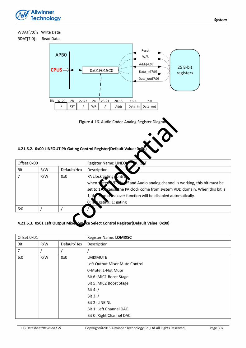
System
H3 Datasheet(Revision1.2) Copyright© 2015 Allwinner Technology Co.,Ltd.All Rights Reserved. Page 307
WDAT[7:0]:Write Data;
RDAT[7:0]: Read Data.
APB0 W/R
Addr[4:0]
Data_in[7:0]
Data_out[7:0]
Bit
RST
2832-29
/
27-23
/
24
WR
15-8
Data_in
7-0
Data_out
20-16
Addr
Reset
23-21
/
25 8-bit registers
CPUS 0x01F015C0
Figure 4-16. Audio Codec Analog Register Diagram
4.21.6.2. 0x00 LINEOUT PA Gating Control Register(Default Value: 0x00)
Offset:0x00 Register Name: LINEOUT_PA_GAT
Bit R/W Default/Hex Description
7 R/W 0x0 PA clock gating control;
when system VDD is off and Audio analog channel is working, this bit must be
set to 1, because the PA clock come from system VDD domain. When this bit is
1, the Zero cross over function will be disabled automatically.
0: not gating; 1: gating
6:0 / / /
4.21.6.3. 0x01 Left Output Mixer Source Select Control Register(Default Value: 0x00)
Offset:0x01 Register Name: LOMIXSC
Bit R/W Default/Hex Description
7 / / /
6:0 R/W 0x0 LMIXMUTE
Left Output Mixer Mute Control
0-Mute, 1-Not Mute
Bit 6: MIC1 Boost Stage
Bit 5: MIC2 Boost Stage
Bit 4: /
Bit 3: /
Bit 2: LINEINL
Bit 1: Left Channel DAC
Bit 0: Right Channel DAC
confid
ential
System
H3 Datasheet(Revision1.2) Copyright© 2015 Allwinner Technology Co.,Ltd.All Rights Reserved. Page 308
4.21.6.4. 0x02 Right Output Mixer Source Select Control Register(Default Value: 0x00)
Offset:0x02 Register Name: ROMIXSC
Bit R/W Default/Hex Description
7 / / /
6:0 R/W 0x0 RMIXMUTE
Right Output Mixer Mute Control
0-Mute, 1-Not Mute
Bit 6: MIC1 Boost Stage
Bit 5: MIC2 Boost Stage
Bit 4: /
Bit 3: /
Bit 2: LINEINR
Bit 1: Right Channel DAC
Bit 0: Left Channel DAC
4.21.6.5. 0x03 DAC Analog Enable and PA Source Control Register(Default Value: 0x00)
Offset:0x03 Register Name: DAC_PA_SRC
Bit R/W Default/Hex Description
7 R/W 0x0 DACAREN
Internal Analog Right channel DAC Enable
0:Disable; 1:Enable
6 R/W 0x0 DACALEN
Internal Analog Left channel DAC Enable
0:Disable; 1:Enable
5 R/W 0 RMIXEN
Right Analog Output Mixer Enable
0:Disable; 1:Enable
4 R/W 0x0 LMIXEN
Left Analog Output Mixer Enable
0:Disable; 1:Enable
3:0 / / /
4.21.6.6. 0x05 Linein and Gain Control Register(Default Value: 0x30)
Offset:0x05 Register Name: LINEIN_GCTR
Bit R/W Default/Hex Description
7 / / /
6:4 R/W 0x3 LINEING, (volln)
LINEINL/R to L/R output mixer Gain Control
From -4.5dB to 6dB, 1.5dB/step, default is 0dB
confid
ential
System
H3 Datasheet(Revision1.2) Copyright© 2015 Allwinner Technology Co.,Ltd.All Rights Reserved. Page 309
3:0 / / /
4.21.6.7. 0x06 MIC1 And MIC2 Gain Control Register(Default Value: 0x33)
Offset:0x06 Register Name: MIC_GCTR
Bit R/W Default/Hex Description
7 / / /
6:4 R/W 0x3 MIC1_GAIN
MIC1 BOOST stage to L or R output mixer Gain Control
From -4.5dB to 6dB, 1.5dB/step, default is 0dB
3 / / /
2:0 R/W 0x3 MIC2G, (volm2)
MIC2 BOOST stage to L or R output mixer Gain Control
From -4.5dB to 6dB, 1.5dB/step, default is 0dB
4.21.6.8. 0x07 PA Enable and LINEOUT Control Register(Default Value: 0x04)
Offset:0x07 Register Name: PAEN_CTR
Bit R/W Default/Hex Description
7 R/W 0x0 LINEOUTEN
Right & Left LINEOUT Enable
0-disable
1-enable
6:4 / / /
3:2 R/W 0x1 PA_ANTI_POP_CTRL, (slopelengthsel)
PA Anti-pop time Control
00:131ms; 01: 262ms; 10: 393ms; 11:524ms
1:0 / / /
4.21.6.9. 0x09 Lineout Volume Control Register(Default Value: 0x00)
Offset:0x09 Register Name: LINEOUT_VOLC
Bit R/W Default/Hex Description
7:3 R/W 0x0 LINEOUTVOL
Line-out Volume Control, Total 31 level, from 0dB to -48dB, 1.5dB/step, mute
when 00000 & 00001
2:0 / / /
confid
ential
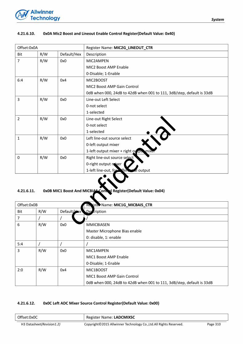
System
H3 Datasheet(Revision1.2) Copyright© 2015 Allwinner Technology Co.,Ltd.All Rights Reserved. Page 310
4.21.6.10. 0x0A Mic2 Boost and Lineout Enable Control Register(Default Value: 0x40)
Offset:0x0A Register Name: MIC2G_LINEOUT_CTR
Bit R/W Default/Hex Description
7 R/W 0x0 MIC2AMPEN
MIC2 Boost AMP Enable
0-Disable; 1-Enable
6:4 R/W 0x4 MIC2BOOST
MIC2 Boost AMP Gain Control
0dB when 000, 24dB to 42dB when 001 to 111, 3dB/step, default is 33dB
3 R/W 0x0 Line-out Left Select
0-not select
1-selected
2 R/W 0x0 Line-out Right Select
0-not select
1-selected
1 R/W 0x0 Left line-out source select
0-left output mixer
1-left output mixer + right output mixer
0 R/W 0x0 Right line-out source select
0-right output mixer
1-left line-out, for differential output
4.21.6.11. 0x0B MIC1 Boost And MICBIAS Control Register(Default Value: 0x04)
Offset:0x0B Register Name: MIC1G_MICBAIS_CTR
Bit R/W Default/Hex Description
7 / / /
6 R/W 0x0 MMICBIASEN
Master Microphone Bias enable
0: disable, 1: enable
5:4 / / /
3 R/W 0x0 MIC1AMPEN
MIC1 Boost AMP Enable
0-Disable; 1-Enable
2:0 R/W 0x4 MIC1BOOST
MIC1 Boost AMP Gain Control
0dB when 000, 24dB to 42dB when 001 to 111, 3dB/step, default is 33dB
4.21.6.12. 0x0C Left ADC Mixer Source Control Register(Default Value: 0x00)
Offset:0x0C Register Name: LADCMIXSC
confid
ential

System
H3 Datasheet(Revision1.2) Copyright© 2015 Allwinner Technology Co.,Ltd.All Rights Reserved. Page 311
Bit R/W Default/Hex Description
7 / / /
6:0 R/W 0x0 RADCMIXMUTE
Right ADC Mixer Mute Control:
0-Mute, 1-Not Mute
Bit 6: MIC1 Boost Stage
Bit 5: MIC2 Boost Stage
Bit 4: /
Bit 3:/
Bit 2: LINEINL
Bit 1: Left Output Mixer
Bit 0: Right Output Mixer
4.21.6.13. 0x0D Right ADC Mixer Source Control Register(Default Value: 0x00)
Offset:0x0D Register Name: RADCMIXSC
Bit R/W Default/Hex Description
7 / / /
6:0 R/W 0x0 RADCMIXMUTE
Right ADC Mixer Mute Control:
0-Mute, 1-Not Mute
Bit 6: MIC1 Boost Stage
Bit 5: MIC2 Boost Stage
Bit 4: /
Bit 3:/
Bit 2: LINEINR
Bit 1: Right Output Mixer
Bit 0: Left Output Mixer
4.21.6.14. 0x0E Reserved Register(Default Value: 0x04)
Offset:0x0E Register Name: Res_Reg
Bit R/W Default/Hex Description
7:6 / / /
5:4 R/W 0x0 MBIASSEL
MMICBIAS voltage level select
00: 1.88V
01: 2.09V
10: 2.33V
11: 2.50V
3 / / /
2:0 R/W 0x4 PA_ANTI_POP
confid
ential

System
H3 Datasheet(Revision1.2) Copyright© 2015 Allwinner Technology Co.,Ltd.All Rights Reserved. Page 312
PA ANTI-POP Time Control
000: 131ms
001: 262ms
010: 393ms
011: 524ms
100: 655ms
101: 786ms
110: 917ms
111: 1048ms
4.21.6.15. 0x0F ADC Analog Part Enable Register(Default Value: 0x03)
Offset:0x0F Register Name: ADC_AP_EN
Bit R/W Default/Hex Description
7 R/W 0x0 ADCREN
ADC Right Channel Enable
0-Disable; 1-Enable
6 R/W 0x0 ADCLEN
ADC Left Channel Enable
0-Disable; 1-Enable
5:3 / / /
2:0 R/W 0x3 ADCG
ADC Input Gain Control
From -4.5dB to 6dB, 1.5dB/step default is 0dB
4.21.6.16. 0x10 ADDA Analog Performance Turning 0 Register(Default Value: 0x55)
Offset:0x10 Register Name: ADDA_APT0
Bit R/W Default/Hex Description
7:6 R/W 0x1 OPDRV_OPCOM_CUR.
OPDRV/OPCOM output stage current setting
5:4 R/W 0x1 OPADC1_BIAS_CUR.
OPADC1 Bias Current Select
3:2 R/W 0x1 OPADC2_BIAS_CUR.
OPADC2 Bias Current Select
1:0 R/W 0x1 OPAAF_BIAS_CUR.
OPAAF in ADC Bias Current Select
4.21.6.17. 0x11 ADDA Analog Performance Turning 1 Register(Default Value: 0x45)
Offset:0x11 Register Name: ADDA_APT1
confid
ential

System
H3 Datasheet(Revision1.2) Copyright© 2015 Allwinner Technology Co.,Ltd.All Rights Reserved. Page 313
Bit R/W Default/Hex Description
7:6 R/W 0x1 OPMIC_BIAS_CUR
OPMIC Bias Current Control
5:4 / / /
3:2 R/W 0x1 OPDAC_BIAS_CUR.
OPDAC Bias Current Control
1:0 R/W 0x1 OPMIX_BIAS_CUR.
OPMIX/OPLPF Bias Current Control
4.21.6.18. 0x12 ADDA Analog Performance Turning 2 Register(Default Value: 0x42)
Offset:0x12 Register Name: ADDA_APT2
Bit R/W Default/Hex Description
7 R/W 0x0 function enable for master volume change at zero cross over
0: disable; 1: enable
6 R/W 0x1 Timeout control for master volume change at zero cross over
0: 32ms; 1: 64ms
5:4 R/W 0x0 PTDBS
HPCOM protect de-bounce time setting
00: 2-3ms; 01: 4-6ms; 10: 8-12ms; 11: 16-24ms
at the same time, bit 17 is used to control the AVCCPORFLAG, write 1 to this bit,
flag will be clear, and the calibration is done again
3 R/W 0x0 PA_SLOPE_SELECT
PA slope select cosine or ramp
0: select cosine
1: select ramp
2:0 R/W 0x2 USB_BIAS_CUR.
USB bias current tuning
From 23uA to 30uA, Default is 25uA
4.21.6.19. 0x13 Bias & DA16 Calibration Control Register0(Default Value: 0xD6)
Offset:0x13 Register Name: Bias_DA16_CAL_CTR0
Bit R/W Default/Hex Description
7 R/W 0x1 MMIC BIAS chopper enable
0: disable; 1:enable
6:5 R/W 0x2 MMIC BIAS chopper clock select
00: 250KHz; 01: 500KHz; 10: 1MHz; 11: 2MHz
4 R/W 0x1 DITHER
ADC dither on/off control
0: dither off; 1: dither on
3:2 R/W 0x1 DITHER_CLK_SELECT
confid
ential
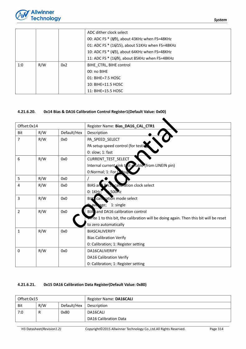
System
H3 Datasheet(Revision1.2) Copyright© 2015 Allwinner Technology Co.,Ltd.All Rights Reserved. Page 314
ADC dither clock select
00: ADC FS * (8/9), about 43KHz when FS=48KHz
01: ADC FS * (16/15), about 51KHz when FS=48KHz
10: ADC FS * (4/3), about 64KHz when FS=48KHz
11: ADC FS * (16/9), about 85KHz when FS=48KHz
1:0 R/W 0x2 BIHE_CTRL, BIHE control
00: no BIHE
01: BIHE=7.5 HOSC
10: BIHE=11.5 HOSC
11: BIHE=15.5 HOSC
4.21.6.20. 0x14 Bias & DA16 Calibration Control Register1(Default Value: 0x00)
Offset:0x14 Register Name: Bias_DA16_CAL_CTR1
Bit R/W Default/Hex Description
7 R/W 0x0 PA_SPEED_SELECT
PA setup speed control (for testing)
0: slow; 1: fast
6 R/W 0x0 CURRENT_TEST_SELECT
Internal current sink test enable (from LINEIN pin)
0:Normal; 1: For Debug
5 R/W 0x0 /
4 R/W 0x0 BIAS and DA16 calibration clock select
0: 1KHz; 1: 500Hz
3 R/W 0x0 BIAS calibration mode select
0: average; 1: single
2 R/W 0x0 BIAS and DA16 calibration control
Write 1 to this bit, the calibration will be doing again. Then this bit will be reset
to zero automatically
1 R/W 0x0 BIASCALIVERIFY
Bias Calibration Verify
0: Calibration; 1: Register setting
0 R/W 0x0 DA16CALIVERIFY
DA16 Calibration Verify
0: Calibration; 1: Register setting
4.21.6.21. 0x15 DA16 Calibration Data Register(Default Value: 0x80)
Offset:0x15 Register Name: DA16CALI
Bit R/W Default/Hex Description
7:0 R 0x80 DA16CALI
DA16 Calibration Data
confid
ential
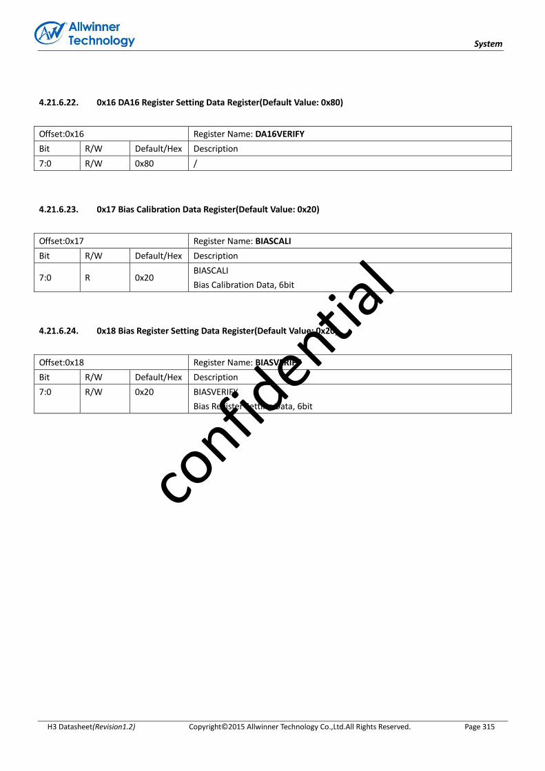
System
H3 Datasheet(Revision1.2) Copyright© 2015 Allwinner Technology Co.,Ltd.All Rights Reserved. Page 315
4.21.6.22. 0x16 DA16 Register Setting Data Register(Default Value: 0x80)
Offset:0x16 Register Name: DA16VERIFY
Bit R/W Default/Hex Description
7:0 R/W 0x80 /
4.21.6.23. 0x17 Bias Calibration Data Register(Default Value: 0x20)
Offset:0x17 Register Name: BIASCALI
Bit R/W Default/Hex Description
7:0 R 0x20 BIASCALI
Bias Calibration Data, 6bit
4.21.6.24. 0x18 Bias Register Setting Data Register(Default Value: 0x20)
Offset:0x18 Register Name: BIASVERIFY
Bit R/W Default/Hex Description
7:0 R/W 0x20 BIASVERIFY
Bias Register Setting Data, 6bit
confid
ential
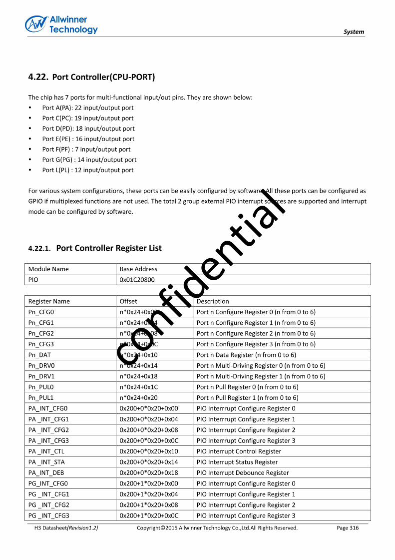
System
H3 Datasheet(Revision1.2) Copyright© 2015 Allwinner Technology Co.,Ltd.All Rights Reserved. Page 316
4.22. Port Controller(CPU-PORT)
The chip has 7 ports for multi-functional input/out pins. They are shown below:
Port A(PA): 22 input/output port
Port C(PC): 19 input/output port
Port D(PD): 18 input/output port
Port E(PE) : 16 input/output port
Port F(PF) : 7 input/output port
Port G(PG) : 14 input/output port
Port L(PL) : 12 input/output port
For various system configurations, these ports can be easily configured by software. All these ports can be configured as
GPIO if multiplexed functions are not used. The total 2 group external PIO interrupt sources are supported and interrupt
mode can be configured by software.
4.22.1. Port Controller Register List
Module Name Base Address
PIO 0x01C20800
Register Name Offset Description
Pn_CFG0 n*0x24+0x00 Port n Configure Register 0 (n from 0 to 6)
Pn_CFG1 n*0x24+0x04 Port n Configure Register 1 (n from 0 to 6)
Pn_CFG2 n*0x24+0x08 Port n Configure Register 2 (n from 0 to 6)
Pn_CFG3 n*0x24+0x0C Port n Configure Register 3 (n from 0 to 6)
Pn_DAT n*0x24+0x10 Port n Data Register (n from 0 to 6)
Pn_DRV0 n*0x24+0x14 Port n Multi-Driving Register 0 (n from 0 to 6)
Pn_DRV1 n*0x24+0x18 Port n Multi-Driving Register 1 (n from 0 to 6)
Pn_PUL0 n*0x24+0x1C Port n Pull Register 0 (n from 0 to 6)
Pn_PUL1 n*0x24+0x20 Port n Pull Register 1 (n from 0 to 6)
PA_INT_CFG0 0x200+0*0x20+0x00 PIO Interrrupt Configure Register 0
PA _INT_CFG1 0x200+0*0x20+0x04 PIO Interrrupt Configure Register 1
PA _INT_CFG2 0x200+0*0x20+0x08 PIO Interrrupt Configure Register 2
PA _INT_CFG3 0x200+0*0x20+0x0C PIO Interrrupt Configure Register 3
PA _INT_CTL 0x200+0*0x20+0x10 PIO Interrupt Control Register
PA _INT_STA 0x200+0*0x20+0x14 PIO Interrupt Status Register
PA_INT_DEB 0x200+0*0x20+0x18 PIO Interrupt Debounce Register
PG_INT_CFG0 0x200+1*0x20+0x00 PIO Interrrupt Configure Register 0
PG _INT_CFG1 0x200+1*0x20+0x04 PIO Interrrupt Configure Register 1
PG _INT_CFG2 0x200+1*0x20+0x08 PIO Interrrupt Configure Register 2
PG _INT_CFG3 0x200+1*0x20+0x0C PIO Interrrupt Configure Register 3
confid
ential
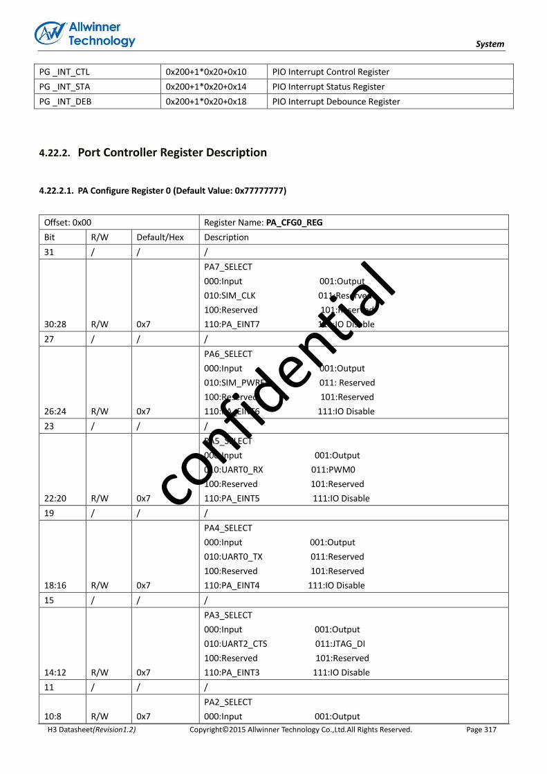
System
H3 Datasheet(Revision1.2) Copyright© 2015 Allwinner Technology Co.,Ltd.All Rights Reserved. Page 317
PG _INT_CTL 0x200+1*0x20+0x10 PIO Interrupt Control Register
PG _INT_STA 0x200+1*0x20+0x14 PIO Interrupt Status Register
PG _INT_DEB 0x200+1*0x20+0x18 PIO Interrupt Debounce Register
4.22.2. Port Controller Register Description
4.22.2.1. PA Configure Register 0 (Default Value: 0x77777777)
Offset: 0x00 Register Name: PA_CFG0_REG
Bit R/W Default/Hex Description
31 / / /
30:28 R/W 0x7
PA7_SELECT
000:Input 001:Output
010:SIM_CLK 011:Reserved
100:Reserved 101:Reserved
110:PA_EINT7 111:IO Disable
27 / / /
26:24 R/W 0x7
PA6_SELECT
000:Input 001:Output
010:SIM_PWREN 011: Reserved
100:Reserved 101:Reserved
110:PA_EINT6 111:IO Disable
23 / / /
22:20 R/W 0x7
PA5_SELECT
000:Input 001:Output
010:UART0_RX 011:PWM0
100:Reserved 101:Reserved
110:PA_EINT5 111:IO Disable
19 / / /
18:16 R/W 0x7
PA4_SELECT
000:Input 001:Output
010:UART0_TX 011:Reserved
100:Reserved 101:Reserved
110:PA_EINT4 111:IO Disable
15 / / /
14:12 R/W 0x7
PA3_SELECT
000:Input 001:Output
010:UART2_CTS 011:JTAG_DI
100:Reserved 101:Reserved
110:PA_EINT3 111:IO Disable
11 / / /
10:8 R/W 0x7
PA2_SELECT
000:Input 001:Output
confid
ential
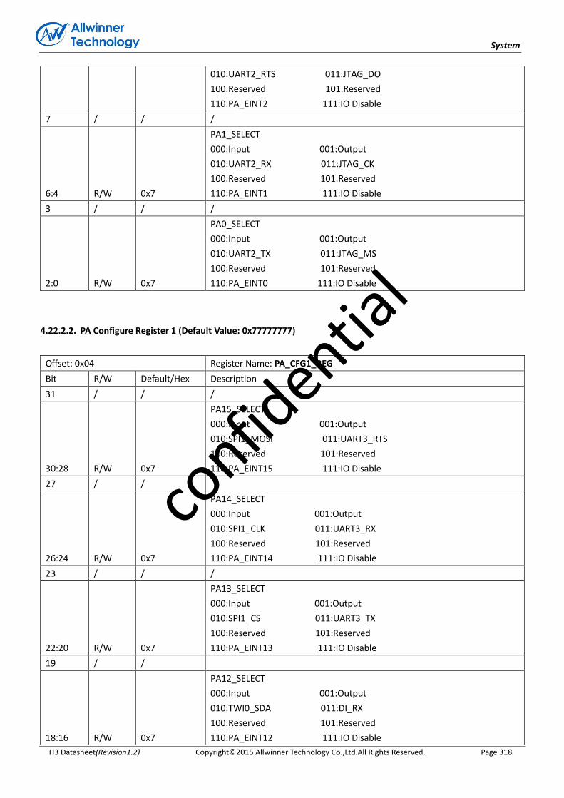
System
H3 Datasheet(Revision1.2) Copyright© 2015 Allwinner Technology Co.,Ltd.All Rights Reserved. Page 318
010:UART2_RTS 011:JTAG_DO
100:Reserved 101:Reserved
110:PA_EINT2 111:IO Disable
7 / / /
6:4 R/W 0x7
PA1_SELECT
000:Input 001:Output
010:UART2_RX 011:JTAG_CK
100:Reserved 101:Reserved
110:PA_EINT1 111:IO Disable
3 / / /
2:0 R/W 0x7
PA0_SELECT
000:Input 001:Output
010:UART2_TX 011:JTAG_MS
100:Reserved 101:Reserved
110:PA_EINT0 111:IO Disable
4.22.2.2. PA Configure Register 1 (Default Value: 0x77777777)
Offset: 0x04 Register Name: PA_CFG1_REG
Bit R/W Default/Hex Description
31 / / /
30:28 R/W 0x7
PA15_SELECT
000:Input 001:Output
010:SPI1_MOSI 011:UART3_RTS
100:Reserved 101:Reserved
110:PA_EINT15 111:IO Disable
27 / /
26:24 R/W 0x7
PA14_SELECT
000:Input 001:Output
010:SPI1_CLK 011:UART3_RX
100:Reserved 101:Reserved
110:PA_EINT14 111:IO Disable
23 / / /
22:20 R/W 0x7
PA13_SELECT
000:Input 001:Output
010:SPI1_CS 011:UART3_TX
100:Reserved 101:Reserved
110:PA_EINT13 111:IO Disable
19 / /
18:16 R/W 0x7
PA12_SELECT
000:Input 001:Output
010:TWI0_SDA 011:DI_RX
100:Reserved 101:Reserved
110:PA_EINT12 111:IO Disable
confid
ential
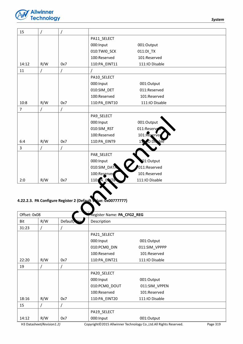
System
H3 Datasheet(Revision1.2) Copyright© 2015 Allwinner Technology Co.,Ltd.All Rights Reserved. Page 319
15 / /
14:12 R/W 0x7
PA11_SELECT
000:Input 001:Output
010:TWI0_SCK 011:DI_TX
100:Reserved 101:Reserved
110:PA_EINT11 111:IO Disable
11 / / /
10:8 R/W 0x7
PA10_SELECT
000:Input 001:Output
010:SIM_DET 011:Reserved
100:Reserved 101:Reserved
110:PA_EINT10 111:IO Disable
7 / /
6:4 R/W 0x7
PA9_SELECT
000:Input 001:Output
010:SIM_RST 011:Reserved
100:Reserved 101:Reserved
110:PA_EINT9 111:IO Disable
3 / /
2:0 R/W 0x7
PA8_SELECT
000:Input 001:Output
010:SIM_DATA 011:Reserved
100:Reserved 101:Reserved
110:PA_EINT8 111:IO Disable
4.22.2.3. PA Configure Register 2 (Default Value: 0x00777777)
Offset: 0x08 Register Name: PA_CFG2_REG
Bit R/W Default/Hex Description
31:23 / /
22:20 R/W 0x7
PA21_SELECT
000:Input 001:Output
010:PCM0_DIN 011:SIM_VPPPP
100:Reserved 101:Reserved
110:PA_EINT21 111:IO Disable
19 / /
18:16 R/W 0x7
PA20_SELECT
000:Input 001:Output
010:PCM0_DOUT 011:SIM_VPPEN
100:Reserved 101:Reserved
110:PA_EINT20 111:IO Disable
15 / /
14:12 R/W 0x7
PA19_SELECT
000:Input 001:Output
confid
ential

System
H3 Datasheet(Revision1.2) Copyright© 2015 Allwinner Technology Co.,Ltd.All Rights Reserved. Page 320
010:PCM0_CLK 011:TWI1_SDA
100:Reserved 101:Reserved
110:PA_EINT19 111:IO Disable
11 / / /
10:8 R/W 0x7
PA18_SELECT
000:Input 001:Output
010:PCM0_SYNC 011:TWI1_SCK
100:Reserved 101:Reserved
110:PA_EINT18 111:IO Disable
7 / /
6:4 R/W 0x7
PA17_SELECT
000:Input 001:Output
010:OWA_OUT 011:Reserved
100:Reserved 101:Reserved
110:PA_EINT17 111:IO Disable
3 / /
2:0 R/W 0x7
PA16_SELECT
000:Input 001:Output
010:SPI1_MISO 011:UART3_CTS
100:Reserved 101:Reserved
110:PA_EINT16 111:IO Disable
4.22.2.4. PA Configure Register 3 (Default Value: 0x00000000)
Offset: 0x0C Register Name: PA_CFG3_REG
Bit R/W Default/Hex Description
31:0 / / /
4.22.2.5. PA Data Register (Default Value: 0x00000000)
Offset: 0x10 Register Name: PA_DATA_REG
Bit R/W Default/Hex Description
31:22 / / /
21:0 R/W 0x0
PA_DAT
If the port is configured as input, the corresponding bit is the pin state. If
the port is configured as output, the pin state is the same as the
corresponding bit. The read bit value is the value setup by software. If the
port is configured as functional pin, the undefined value will be read.
confid
ential
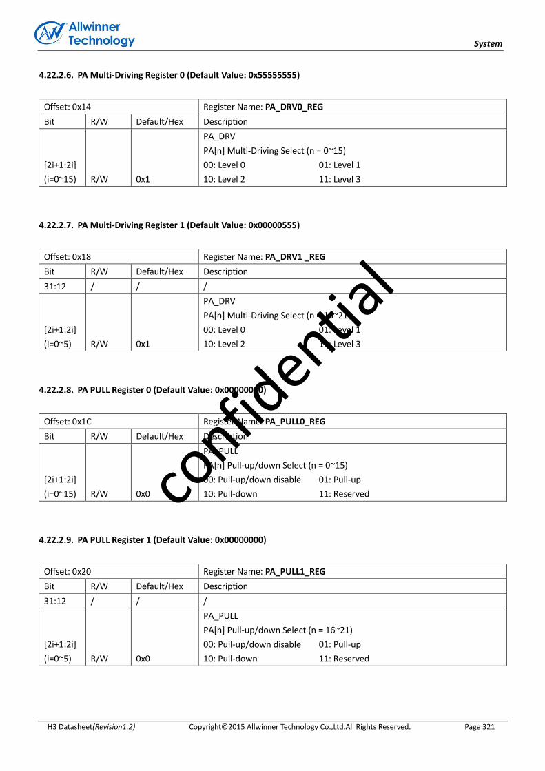
System
H3 Datasheet(Revision1.2) Copyright© 2015 Allwinner Technology Co.,Ltd.All Rights Reserved. Page 321
4.22.2.6. PA Multi-Driving Register 0 (Default Value: 0x55555555)
Offset: 0x14 Register Name: PA_DRV0_REG
Bit R/W Default/Hex Description
[2i+1:2i]
(i=0~15) R/W 0x1
PA_DRV
PA[n] Multi-Driving Select (n = 0~15)
00: Level 0 01: Level 1
10: Level 2 11: Level 3
4.22.2.7. PA Multi-Driving Register 1 (Default Value: 0x00000555)
Offset: 0x18 Register Name: PA_DRV1 _REG
Bit R/W Default/Hex Description
31:12 / / /
[2i+1:2i]
(i=0~5) R/W 0x1
PA_DRV
PA[n] Multi-Driving Select (n = 16~21)
00: Level 0 01: Level 1
10: Level 2 11: Level 3
4.22.2.8. PA PULL Register 0 (Default Value: 0x00000000)
Offset: 0x1C Register Name: PA_PULL0_REG
Bit R/W Default/Hex Description
[2i+1:2i]
(i=0~15) R/W 0x0
PA_PULL
PA[n] Pull-up/down Select (n = 0~15)
00: Pull-up/down disable 01: Pull-up
10: Pull-down 11: Reserved
4.22.2.9. PA PULL Register 1 (Default Value: 0x00000000)
Offset: 0x20 Register Name: PA_PULL1_REG
Bit R/W Default/Hex Description
31:12 / / /
[2i+1:2i]
(i=0~5) R/W 0x0
PA_PULL
PA[n] Pull-up/down Select (n = 16~21)
00: Pull-up/down disable 01: Pull-up
10: Pull-down 11: Reserved
confid
ential

System
H3 Datasheet(Revision1.2) Copyright© 2015 Allwinner Technology Co.,Ltd.All Rights Reserved. Page 322
4.22.2.10. PC Configure Register 0 (Default Value: 0x77777777)
Offset: 0x48 Register Name: PC_CFG0_REG
Bit R/W Default/Hex Description
31 / / /
30:28 R/W 0x7
PC7_SELECT
000:Input 001:Output
010:NAND_RB1 011:Reserved
100:Reserved 101:Reserved
110:Reserved 111:IO Disable
27 / / /
26:24 R/W 0x7
PC6_SELECT
000:Input 001:Output
010:NAND_RB0 011:SDC2_CMD
100:Reserved 101:Reserved
110:Reserved 111:IO Disable
23 / / /
22:20 R/W 0x7
PC5_SELECT
000:Input 001:Output
010:NAND_RE 011:SDC2_CLK
100:Reserved 101:Reserved
110:Reserved 111:IO Disable
19 / / /
18:16 R/W 0x7
PC4_SELECT
000:Input 001:Output
010:NAND_CE0 011:Reserved
100:Reserved 101:Reserved
110:Reserved 111:IO Disable
15 / / /
14:12 R/W 0x7
PC3_SELECT
000:Input 001:Output
010:NAND_CE1 011:SPI0_CS
100:Reserved 101:Reserved
110:Reserved 111:IO Disable
11 / / /
10:8 R/W 0x7
PC2_SELECT
000:Input 001:Output
010:NAND_CLE 011:SPI0_CLK
100:Reserved 101:Reserved
110:Reserved 111:IO Disable
7 / / /
6:4 R/W 0x7
PC1_SELECT
000:Input 001:Output
010:NAND_ALE 011:SPI0_MISO
confid
ential

System
H3 Datasheet(Revision1.2) Copyright© 2015 Allwinner Technology Co.,Ltd.All Rights Reserved. Page 323
100:Reserved 101:Reserved
110:Reserved 111:IO Disable
3 / / /
2:0 R/W 0x7
PC0_SELECT
000:Input 001:Output
010:NAND_WE 011:SPI0_MOSI
100:Reserved 101:Reserved
110:Reserved 111:IO Disable
4.22.2.11. PC Configure Register 1 (Default Value: 0x77777777)
Offset: 0x4C Register Name: PC_CFG1_REG
Bit R/W Default/Hex Description
31 / / /
30:28 R/W 0x7
PC15_SELECT
000:Input 001:Output
010:NAND_DQ7 011:SDC2_D7
100:Reserved 101:Reserved
110:Reserved 111:IO Disable
27 / / /
26:24 R/W 0x7
PC14_SELECT
000:Input 001:Output
010:NAND_DQ6 011:SDC2_D6
100:Reserved 101:Reserved
110:Reserved 111:IO Disable
23 / / /
22:20 R/W 0x7
PC13_SELECT
000:Input 001:Output
010:NAND_DQ5 011:SDC2_D5
100:Reserved 101:Reserved
110:Reserved 111:IO Disable
19 / / /
18:16 R/W 0x7
PC12_SELECT
000:Input 001:Output
010:NAND_DQ4 011:SDC2_D4
100:Reserved 101:Reserved
110:Reserved 111:IO Disable
15 / / /
14:12 R/W 0x7
PC11_SELECT
000:Input 001:Output
010:NAND_DQ3 011:SDC2_D3
100:Reserved 101:Reserved
110:Reserved 111:IO Disable
11 / / /
confid
ential

System
H3 Datasheet(Revision1.2) Copyright© 2015 Allwinner Technology Co.,Ltd.All Rights Reserved. Page 324
10:8 R/W 0x7
PC10_SELECT
000:Input 001:Output
010:NAND_DQ2 011:SDC2_D2
100:Reserved 101:Reserved
110:Reserved 111:IO Disable
7 / / /
6:4 R/W 0x7
PC9_SELECT
000:Input 001:Output
010:NAND_DQ1 011:SDC2_D1
100:Reserved 101:Reserved
110:Reserved 111:IO Disable
3 / / /
2:0 R/W 0x7
PC8_SELECT
000:Input 001:Output
010:NAND_DQ0 011:SDC2_D0
100:Reserved 101:Reserved
110:Reserved 111:IO Disable
4.22.2.12. PC Configure Register 2 (Default Value: 0x00000777)
Offset: 0x50 Register Name: PC_CFG2_REG
Bit R/W Default/Hex Description
31:11 / / /
10:8 R/W 0x7 /
7 / / /
6:4 R/W 0x7 /
3 / / /
2:0 R/W 0x7
PC16_SELECT
000:Input 001:Output
010:NAND_DQS 011:SDC2_RST
100:Reserved 101:Reserved
110:Reserved 111:IO Disable
4.22.2.13. PC Configure Register 3 (Default Value: 0x00000000)
Offset: 0x54 Register Name: PC_CFG3_REG
Bit R/W Default/Hex Description
31:0 / / /
confid
ential

System
H3 Datasheet(Revision1.2) Copyright© 2015 Allwinner Technology Co.,Ltd.All Rights Reserved. Page 325
4.22.2.14. PC Data Register (Default Value: 0x00000000)
Offset: 0x58 Register Name: PC_DATA_REG
Bit R/W Default/Hex Description
31:19 / / /
18:0 R/W 0x0
PC_DAT
If the port is configured as input, the corresponding bit is the pin state. If
the port is configured as output, the pin state is the same as the
corresponding bit. The read bit value is the value setup by software. If the
port is configured as functional pin, the undefined value will be read.
4.22.2.15. PC Multi-Driving Register 0 (Default Value: 0x55555555)
Offset: 0x5C Register Name: PC_DRV0_REG
Bit R/W Default/Hex Description
[2i+1:2i]
(i=0~15) R/W 0x1
PC_DRV
PC[n] Multi-Driving SELECT (n = 0~15)
00: Level 0 01: Level 1
10: Level 2 11: Level 3
4.22.2.16. PC Multi-Driving Register 1 (Default Value: 0x00000015)
Offset: 0x60 Register Name: PC_DRV1_REG
Bit R/W Default/Hex Description
31:6 / / /
[2i+1:2i]
(i=0~2) R/W 0x1
PC_DRV
PC[n] Multi-Driving Select (n = 16~18)
00: Level 0 01: Level 1
10: Level 2 11: Level 3
4.22.2.17. PC PULL Register 0 (Default Value: 0x00005140)
Offset: 0x64 Register Name: PC_PULL0_REG
Bit R/W Default/Hex Description
[2i+1:2i]
(i=0~15) R/W 0x5140
PC_PULL
PC[n] Pull-up/down Select (n = 0~15)
00: Pull-up/down disable 01: Pull-up
10: Pull-down 11: Reserved
confid
ential

System
H3 Datasheet(Revision1.2) Copyright© 2015 Allwinner Technology Co.,Ltd.All Rights Reserved. Page 326
4.22.2.18. PC PULL Register 1 (Default Value: 0x00000014)
Offset: 0x68 Register Name: PC_PULL1_REG
Bit R/W Default/Hex Description
31:6 / / Reserved
[2i+1:2i]
(i=0~2) R/W 0x14
PC_PULL
PC[n] Pull-up/down Select (n = 16~18)
00: Pull-up/down disable 01: Pull-up
10: Pull-down 11: Reserved
4.22.2.19. PD Configure Register 0 (Default Value: 0x77777777)
Offset: 0x6C Register Name: PD_CFG0_REG
Bit R/W Default/Hex Description
31 / / /
30:28 R/W 0x7
PD7_SELECT
000:Input 001:Output
010:RGMII_TXD3/MII_TXD3/RMII_NULL 011:Reserved
100:Reserved 101:Reserved
110:Reserved 111:IO Disable
27 / / Reserved
26:24 R/W 0x7
PD6_SELECT
000:Input 001:Output
010:RGMII_NULL/MII_RXERR/RMII_RXER 011:Reserved
100:Reserved 101:Reserved
110:Reserved 111:IO Disable
23 / / /
22:20 R/W 0x7
PD5_SELECT
000:Input 001:Output
010:RGMII_RXCTL/MII_RXDV/RMII_NULL 011:Reserved
100:Reserved 101:Reserved
110:Reserved 111:IO Disable
19 / / /
18:16 R/W 0x7
PD4_SELECT
000:Input 001:Output
010:RGMII_RXCK/MII_RXCK/RMII_NULL 011:Reserved
100:Reserved 101:Reserved
110:Reserved 111:IO Disable
15 / / /
14:12 R/W 0x7
PD3_SELECT
000:Input 001:Output
010:RGMII_RXD0/MII_RXD0/RMII_RXD0 011:Reserved
100:Reserved 101:Reserved
confid
ential
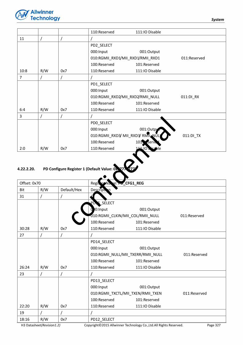
System
H3 Datasheet(Revision1.2) Copyright© 2015 Allwinner Technology Co.,Ltd.All Rights Reserved. Page 327
110:Reserved 111:IO Disable
11 / / /
10:8 R/W 0x7
PD2_SELECT
000:Input 001:Output
010:RGMII_RXD1/MII_RXD1/RMII_RXD1 011:Reserved
100:Reserved 101:Reserved
110:Reserved 111:IO Disable
7 / / /
6:4 R/W 0x7
PD1_SELECT
000:Input 001:Output
010:RGMII_RXD2/MII_RXD2/RMII_NULL 011:DI_RX
100:Reserved 101:Reserved
110:Reserved 111:IO Disable
3 / / /
2:0 R/W 0x7
PD0_SELECT
000:Input 001:Output
010:RGMII_RXD3/ MII_RXD3/ RMII_NULL 011:DI_TX
100:Reserved 101:Reserved
110:Reserved 111:IO Disable
4.22.2.20. PD Configure Register 1 (Default Value: 0x77777777)
Offset: 0x70 Register Name: PD_CFG1_REG
Bit R/W Default/Hex Description
31 / / /
30:28 R/W 0x7
PD15_SELECT
000:Input 001:Output
010:RGMII_CLKIN/MII_COL/RMII_NULL 011:Reserved
100:Reserved 101:Reserved
110:Reserved 111:IO Disable
27 / / /
26:24 R/W 0x7
PD14_SELECT
000:Input 001:Output
010:RGMII_NULL/MII_TXERR/RMII_NULL 011:Reserved
100:Reserved 101:Reserved
110:Reserved 111:IO Disable
23 / / /
22:20 R/W 0x7
PD13_SELECT
000:Input 001:Output
010:RGMII_TXCTL/MII_TXEN/RMII_TXEN 011:Reserved
100:Reserved 101:Reserved
110:Reserved 111:IO Disable
19 / / /
18:16 R/W 0x7 PD12_SELECT
confid
ential

System
H3 Datasheet(Revision1.2) Copyright© 2015 Allwinner Technology Co.,Ltd.All Rights Reserved. Page 328
000:Input 001:Output
010:RGMII_TXCK/MII_TXCK/RMII_TXCK 011:Reserved
100:Reserved 101:Reserved
110:Reserved 111:IO Disable
15 / / /
14:12 R/W 0x7
PD11_SELECT
000:Input 001:Output
010:RGMII_NULL/MII_CRS/RMII_NULL 011:Reserved
100:Reserved 101:Reserved
110:Reserved 111:IO Disable
11 / / /
10:8 R/W 0x7
PD10_SELECT
000:Input 001:Output
010:RGMII_TXD0/MII_TXD0/RMII_TXD0 011:Reserved
100:Reserved 101:Reserved
110:Reserved 111:IO Disable
7 / / /
6:4 R/W 0x7
PD9_SELECT
000:Input 001:Output
010:RGMII_TXD1/MII_TXD1/RMII_TXD1 011:Reserved
100:Reserved 101:Reserved
110:Reserved 111:IO Disable
3 / / /
2:0 R/W 0x7
PD8_SELECT
000:Input 001:Output
010:RGMII_TXD2/MII_TXD2/RMII_NULL 011:Reserved
100:Reserved 101:Reserved
110:Reserved 111:IO Disable
4.22.2.21. PD Configure Register 2 (Default Value: 0x00000077)
Offset: 0x74 Register Name: PD_CFG2_REG
Bit R/W Default/Hex Description
31:7 / / /
6:4 R/W 0x7
PD17_SELECT
000:Input 001:Output
010:MDIO 011:Reserved
100:Reserved 101:Reserved
110:Reserved 111:IO Disable
3 / / /
2:0 R/W 0x7
PD16_SELECT
000:Input 001:Output
010:MDC 011:Reserved
100:Reserved 101:Reserved
confid
ential

System
H3 Datasheet(Revision1.2) Copyright© 2015 Allwinner Technology Co.,Ltd.All Rights Reserved. Page 329
110:Reserved 111:IO Disable
4.22.2.22. PD Configure Register 3 (Default Value: 0x00000000)
Offset: 0x78 Register Name: PD_CFG3_REG
Bit R/W Default/Hex Description
31:0 / / /
4.22.2.23. PD Data Register (Default Value: 0x00000000)
Offset: 0x7C Register Name: PD_DATA _REG
Bit R/W Default/Hex Description
31:18 / / /
17:0 R/W 0x0
PD_DAT
If the port is configured as input, the corresponding bit is the pin state. If
the port is configured as output, the pin state is the same as the
corresponding bit. The read bit value is the value setup by software. If the
port is configured as functional pin, the undefined value will be read.
4.22.2.24. PD Multi-Driving Register 0 (Default Value: 0x55555555)
Offset: 0x80 Register Name: PD_DRV0_REG
Bit R/W Default/Hex Description
[2i+1:2i]
(i=0~15) R/W 0x1
PD_DRV
PD[n] Multi-Driving SELECT (n = 0~15)
00: Level 0 01: Level 1
10: Level 2 11: Level 3
4.22.2.25. PD Multi-Driving Register 1 (Default Value: 0x00000005)
Offset: 0x84 Register Name: PD_DRV1_REG
Bit R/W Default/Hex Description
31:4 / / /
[2i+1:2i]
(i=0~1) R/W 0x1
PD_DRV
PD[n] Multi-Driving Select (n = 16~17)
00: Level 0 01: Level 1
10: Level 2 11: Level 3
confid
ential
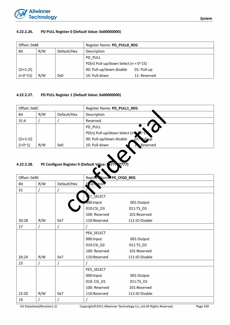
System
H3 Datasheet(Revision1.2) Copyright© 2015 Allwinner Technology Co.,Ltd.All Rights Reserved. Page 330
4.22.2.26. PD PULL Register 0 (Default Value: 0x00000000)
Offset: 0x88 Register Name: PD_PULL0_REG
Bit R/W Default/Hex Description
[2i+1:2i]
(i=0~15) R/W 0x0
PD_PULL
PD[n] Pull-up/down Select (n = 0~15)
00: Pull-up/down disable 01: Pull-up
10: Pull-down 11: Reserved
4.22.2.27. PD PULL Register 1 (Default Value: 0x00000000)
Offset: 0x8C Register Name: PD_PULL1_REG
Bit R/W Default/Hex Description
31:4 / / Reserved
[2i+1:2i]
(i=0~1) R/W 0x0
PD_PULL
PD[n] Pull-up/down Select (n = 16~17)
00: Pull-up/down disable 01: Pull-up
10: Pull-down 11: Reserved
4.22.2.28. PE Configure Register 0 (Default Value: 0x77777777)
Offset: 0x90 Register Name: PE_CFG0_REG
Bit R/W Default/Hex Description
31 / / /
30:28 R/W 0x7
PE7_SELECT
000:Input 001:Output
010:CSI_D3 011:TS_D3
100: Reserved 101:Reserved
110:Reserved 111:IO Disable
27 / / /
26:24 R/W 0x7
PE6_SELECT
000:Input 001:Output
010:CSI_D2 011:TS_D2
100: Reserved 101:Reserved
110:Reserved 111:IO Disable
23 / / /
22:20 R/W 0x7
PE5_SELECT
000:Input 001:Output
010: CSI_D1 011:TS_D1
100: Reserved 101:Reserved
110:Reserved 111:IO Disable
19 / / /
confid
ential
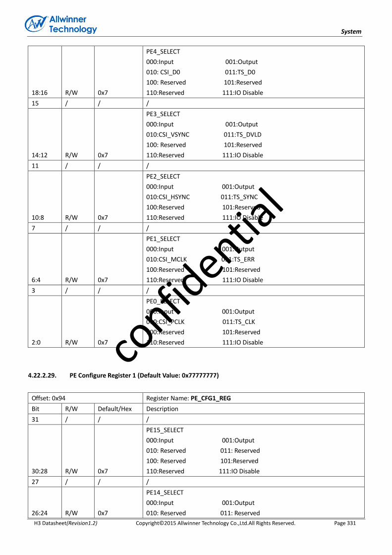
System
H3 Datasheet(Revision1.2) Copyright© 2015 Allwinner Technology Co.,Ltd.All Rights Reserved. Page 331
18:16 R/W 0x7
PE4_SELECT
000:Input 001:Output
010: CSI_D0 011:TS_D0
100: Reserved 101:Reserved
110:Reserved 111:IO Disable
15 / / /
14:12 R/W 0x7
PE3_SELECT
000:Input 001:Output
010:CSI_VSYNC 011:TS_DVLD
100: Reserved 101:Reserved
110:Reserved 111:IO Disable
11 / / /
10:8 R/W 0x7
PE2_SELECT
000:Input 001:Output
010:CSI_HSYNC 011:TS_SYNC
100:Reserved 101:Reserved
110:Reserved 111:IO Disable
7 / / /
6:4 R/W 0x7
PE1_SELECT
000:Input 001:Output
010:CSI_MCLK 011:TS_ERR
100:Reserved 101:Reserved
110:Reserved 111:IO Disable
3 / / /
2:0 R/W 0x7
PE0_SELECT
000:Input 001:Output
010:CSI_PCLK 011:TS_CLK
100:Reserved 101:Reserved
110:Reserved 111:IO Disable
4.22.2.29. PE Configure Register 1 (Default Value: 0x77777777)
Offset: 0x94 Register Name: PE_CFG1_REG
Bit R/W Default/Hex Description
31 / / /
30:28 R/W 0x7
PE15_SELECT
000:Input 001:Output
010: Reserved 011: Reserved
100: Reserved 101:Reserved
110:Reserved 111:IO Disable
27 / / /
26:24 R/W 0x7
PE14_SELECT
000:Input 001:Output
010: Reserved 011: Reserved
confid
ential
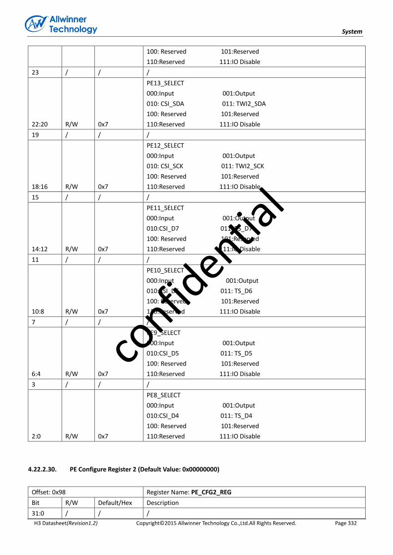
System
H3 Datasheet(Revision1.2) Copyright© 2015 Allwinner Technology Co.,Ltd.All Rights Reserved. Page 332
100: Reserved 101:Reserved
110:Reserved 111:IO Disable
23 / / /
22:20 R/W 0x7
PE13_SELECT
000:Input 001:Output
010: CSI_SDA 011: TWI2_SDA
100: Reserved 101:Reserved
110:Reserved 111:IO Disable
19 / / /
18:16 R/W 0x7
PE12_SELECT
000:Input 001:Output
010: CSI_SCK 011: TWI2_SCK
100: Reserved 101:Reserved
110:Reserved 111:IO Disable
15 / / /
14:12 R/W 0x7
PE11_SELECT
000:Input 001:Output
010:CSI_D7 011: TS_D7
100: Reserved 101:Reserved
110:Reserved 111:IO Disable
11 / / /
10:8 R/W 0x7
PE10_SELECT
000:Input 001:Output
010:CSI_D6 011: TS_D6
100: Reserved 101:Reserved
110:Reserved 111:IO Disable
7 / / /
6:4 R/W 0x7
PE9_SELECT
000:Input 001:Output
010:CSI_D5 011: TS_D5
100: Reserved 101:Reserved
110:Reserved 111:IO Disable
3 / / /
2:0 R/W 0x7
PE8_SELECT
000:Input 001:Output
010:CSI_D4 011: TS_D4
100: Reserved 101:Reserved
110:Reserved 111:IO Disable
4.22.2.30. PE Configure Register 2 (Default Value: 0x00000000)
Offset: 0x98 Register Name: PE_CFG2_REG
Bit R/W Default/Hex Description
31:0 / / /
confid
ential

System
H3 Datasheet(Revision1.2) Copyright© 2015 Allwinner Technology Co.,Ltd.All Rights Reserved. Page 333
4.22.2.31. PE Configure Register 3 (Default Value: 0x00000000)
Offset: 0x9C Register Name: PE_CFG3_REG
Bit R/W Default/Hex Description
31:0 / / /
4.22.2.32. PE Data Register (Default Value: 0x00000000)
Offset: 0xA0 Register Name: PE_DATA _REG
Bit R/W Default/Hex Description
31:16 / / /
15:0 R/W 0x0
PE_DAT
If the port is configured as input, the corresponding bit is the pin state. If
the port is configured as output, the pin state is the same as the
corresponding bit. The read bit value is the value setup by software. If the
port is configured as functional pin, the undefined value will be read.
4.22.2.33. PE Multi-Driving Register 0 (Default Value: 0x55555555)
Offset: 0xA4 Register Name: PE_DRV0_REG
Bit R/W Default/Hex Description
[2i+1:2i]
(i=0~15) R/W 0x1
PE_DRV
PE[n] Multi-Driving SELECT (n = 0~15)
00: Level 0 01: Level 1
10: Level 2 11: Level 3
4.22.2.34. PE Multi-Driving Register 1 (Default Value: 0x00000000)
Offset: 0xA8 Register Name: PE_DRV1_REG
Bit R/W Default/Hex Description
31:0 / / /
4.22.2.35. PE PULL Register 0 (Default Value: 0x00000000)
Offset: 0xAC Register Name: PE_PULL0_REG
Bit R/W Default/Hex Description
[2i+1:2i]
(i=0~15) R/W 0x0
PE_PULL
PE[n] Pull-up/down Select (n = 0~15)
confid
ential

System
H3 Datasheet(Revision1.2) Copyright© 2015 Allwinner Technology Co.,Ltd.All Rights Reserved. Page 334
00: Pull-up/down disable 01: Pull-up
10: Pull-down 11: Reserved
4.22.2.36. PE PULL Register 1 (Default Value: 0x00000000)
Offset: 0xB0 Register Name: PE_PULL1_REG
Bit R/W Default/Hex Description
31:0 / / /
4.22.2.37. PF Configure Register 0 (Default Value: 0x07373733)
Offset: 0xB4 Register Name: PF_CFG0_REG
Bit R/W Default/Hex Description
31:27 / / /
26:24 R/W 0x7
PF6_SELECT
000:Input 001:Output
010: Reserved 011:Reserved
100:Reserved 101:Reserved
110:Reserved 111:IO Disable
23
22:20 R/W 0x3
PF5_SELECT
000:Input 001:Output
010:SDC0_D2 011:JTAG_CK
100:Reserved 101:Reserved
110:Reserved 111:IO Disable
19 / / /
18:16 R/W 0x7
PF4_SELECT
000:Input 001:Output
010:SDC0_D3 011:UART0_RX
100:Reserved 101:Reserved
110:Reserved 111:IO Disable
15 / / /
14:12 R/W 0x3
PF3_SELECT
000:Input 001:Output
010:SDC0_CMD 011:JTAG_DO
100:Reserved 101:Reserved
110:Reserved 111:IO Disable
11 / / /
10:8 R/W 0x7
PF2_SELECT
000:Input 001:Output
010:SDC0_CLK 011:UART0_TX
100:Reserved 101:Reserved
confid
ential
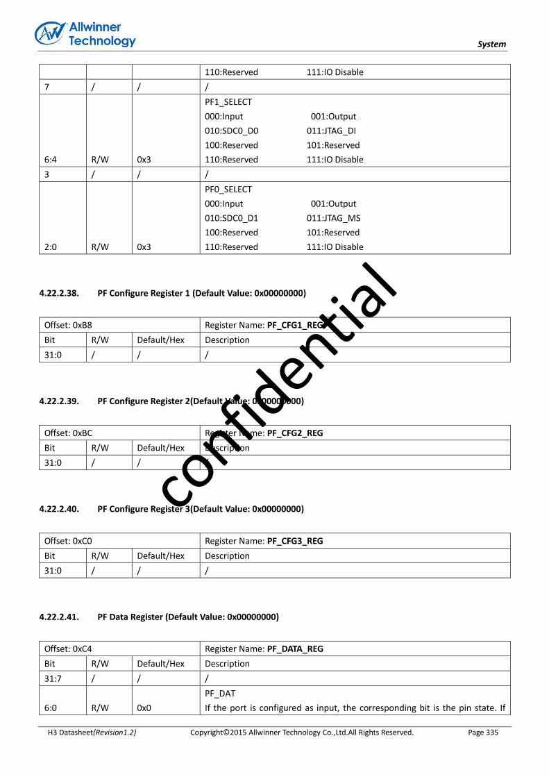
System
H3 Datasheet(Revision1.2) Copyright© 2015 Allwinner Technology Co.,Ltd.All Rights Reserved. Page 335
110:Reserved 111:IO Disable
7 / / /
6:4 R/W 0x3
PF1_SELECT
000:Input 001:Output
010:SDC0_D0 011:JTAG_DI
100:Reserved 101:Reserved
110:Reserved 111:IO Disable
3 / / /
2:0 R/W 0x3
PF0_SELECT
000:Input 001:Output
010:SDC0_D1 011:JTAG_MS
100:Reserved 101:Reserved
110:Reserved 111:IO Disable
4.22.2.38. PF Configure Register 1 (Default Value: 0x00000000)
Offset: 0xB8 Register Name: PF_CFG1_REG
Bit R/W Default/Hex Description
31:0 / / /
4.22.2.39. PF Configure Register 2(Default Value: 0x00000000)
Offset: 0xBC Register Name: PF_CFG2_REG
Bit R/W Default/Hex Description
31:0 / / /
4.22.2.40. PF Configure Register 3(Default Value: 0x00000000)
Offset: 0xC0 Register Name: PF_CFG3_REG
Bit R/W Default/Hex Description
31:0 / / /
4.22.2.41. PF Data Register (Default Value: 0x00000000)
Offset: 0xC4 Register Name: PF_DATA_REG
Bit R/W Default/Hex Description
31:7 / / /
6:0 R/W 0x0
PF_DAT
If the port is configured as input, the corresponding bit is the pin state. If
confid
ential

System
H3 Datasheet(Revision1.2) Copyright© 2015 Allwinner Technology Co.,Ltd.All Rights Reserved. Page 336
the port is configured as output, the pin state is the same as the
corresponding bit. The read bit value is the value setup by software. If the
port is configured as functional pin, the undefined value will be read.
4.22.2.42. PF Multi-Driving Register 0 (Default Value: 0x00001555)
Offset: 0xC8 Register Name: PF_DRV0_REG
Bit R/W Default/Hex Description
31:14 / / /
[2i+1:2i]
(i=0~6) R/W 0x1
PF_DRV
PF[n] Multi-Driving SELECT (n = 0~6)
00: Level 0 01: Level 1
10: Level 2 11: Level 3
4.22.2.43. PF Multi-Driving Register 1 (Default Value: 0x00000000)
Offset: 0xCC Register Name: PF_DRV1_REG
Bit R/W Default/Hex Description
31:0 / / /
4.22.2.44. PF PULL Register 0 (Default Value: 0x00000000)
Offset: 0xD0 Register Name: PF_PULL0_REG
Bit R/W Default/Hex Description
31:14 / / /
[2i+1:2i]
(i=0~6) R/W 0x0
PF_PULL
PF[n] Pull-up/down Select (n = 0~6)
00: Pull-up/down disable 01: Pull-up
10: Pull-down 11: Reserved
4.22.2.45. PF PULL Register 1 (Default Value: 0x00000000)
Offset: 0xD4 Register Name: PF_PULL1_REG
Bit R/W Default/Hex Description
31:0 / / /
confid
ential

System
H3 Datasheet(Revision1.2) Copyright© 2015 Allwinner Technology Co.,Ltd.All Rights Reserved. Page 337
4.22.2.46. PG Configure Register 0 (Default Value: 0x77777777)
Offset: 0xD8 Register Name: PG_CFG0_REG
Bit R/W Default/Hex Description
31 / / /
30:28 R/W 0x7
PG7_SELECT
000:Input 001:Output
010:UART1_RX 011: Reserved
100:Reserved 101:Reserved
110:PG_EINT7 111:IO Disable
27 / / /
26:24 R/W 0x7
PG6_SELECT
000:Input 001:Output
010:UART1_TX 011: Reserved
100:Reserved 101:Reserved
110:PG_EINT6 111:IO Disable
23 / / /
22:20 R/W 0x7
PG5_SELECT
000:Input 001:Output
010:SDC1_D3 011:Reserved
100:Reserved 101:Reserved
110:PG_EINT5 111:IO Disable
19 / / /
18:16 R/W 0x7
PG4_SELECT
000:Input 001:Output
010:SDC1_D2 011:Reserved
100:Reserved 101:Reserved
110:PG_EINT4 111:IO Disable
15 / / /
14:12 R/W 0x7
PG3_SELECT
000:Input 001:Output
010:SDC1_D1 011:Reserved
100:Reserved 101:Reserved
110:PG_EINT3 111:IO Disable
11 / / /
10:8 R/W 0x7
PG2_SELECT
000:Input 001:Output
010:SDC1_D0 011:Reserved
100:Reserved 101:Reserved
110:PG_EINT2 111:IO Disable
7 / / /
6:4 R/W 0x7
PG1_SELECT
000:Input 001:Output
010:SDC1_CMD 011:Reserved
confid
ential
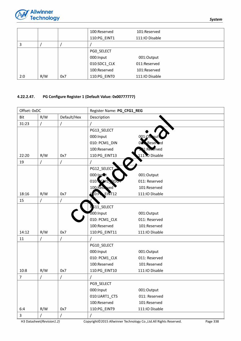
System
H3 Datasheet(Revision1.2) Copyright© 2015 Allwinner Technology Co.,Ltd.All Rights Reserved. Page 338
100:Reserved 101:Reserved
110:PG_EINT1 111:IO Disable
3 / / /
2:0 R/W 0x7
PG0_SELECT
000:Input 001:Output
010:SDC1_CLK 011:Reserved
100:Reserved 101:Reserved
110:PG_EINT0 111:IO Disable
4.22.2.47. PG Configure Register 1 (Default Value: 0x00777777)
Offset: 0xDC Register Name: PG_CFG1_REG
Bit R/W Default/Hex Description
31:23 / / /
22:20 R/W 0x7
PG13_SELECT
000:Input 001:Output
010: PCM1_DIN 011: Reserved
100:Reserved 101:Reserved
110:PG_EINT13 111:IO Disable
19 / / /
18:16 R/W 0x7
PG12_SELECT
000:Input 001:Output
010: PCM1_DOUT 011: Reserved
100:Reserved 101:Reserved
110:PG_EINT12 111:IO Disable
15 / / /
14:12 R/W 0x7
PG11_SELECT
000:Input 001:Output
010: PCM1_CLK 011: Reserved
100:Reserved 101:Reserved
110:PG_EINT11 111:IO Disable
11 / / /
10:8 R/W 0x7
PG10_SELECT
000:Input 001:Output
010: PCM1_CLK 011: Reserved
100:Reserved 101:Reserved
110:PG_EINT10 111:IO Disable
7 / / /
6:4 R/W 0x7
PG9_SELECT
000:Input 001:Output
010:UART1_CTS 011: Reserved
100:Reserved 101:Reserved
110:PG_EINT9 111:IO Disable
3 / / /
confid
ential
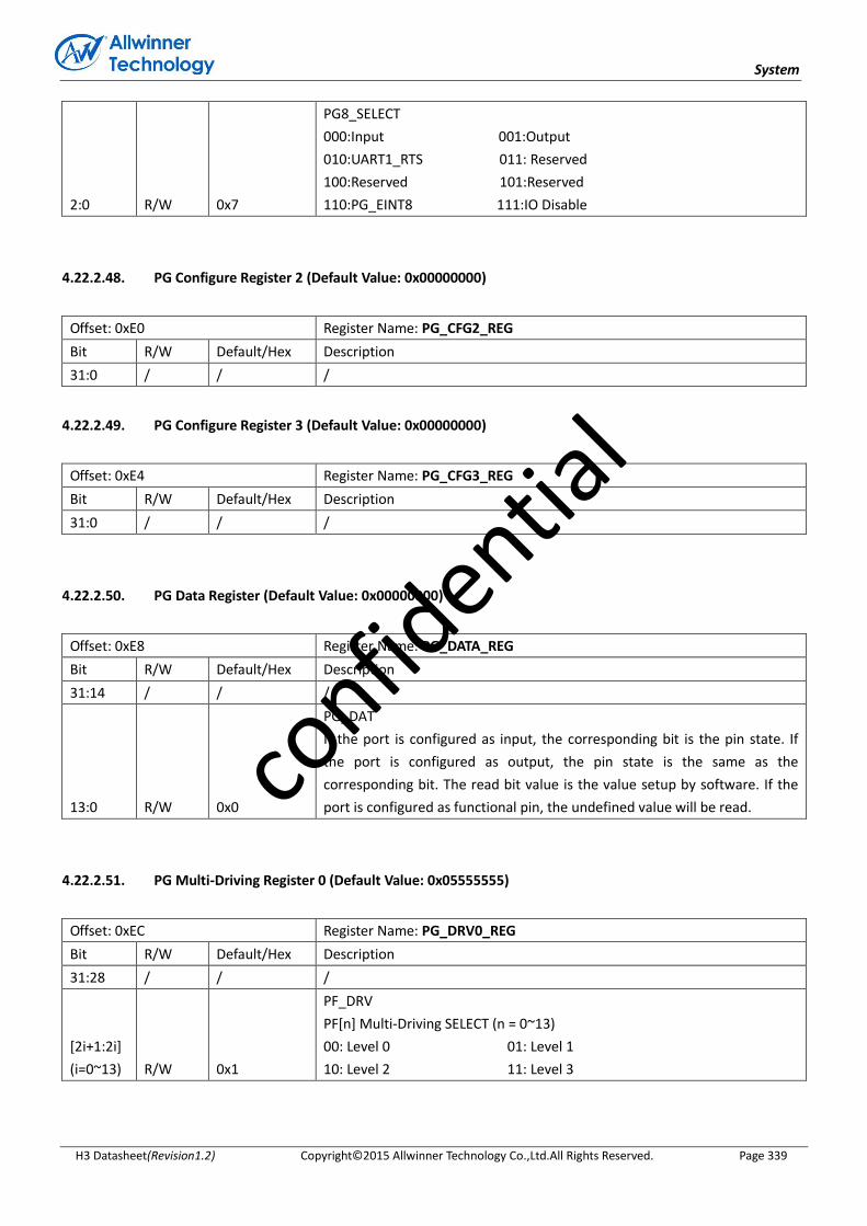
System
H3 Datasheet(Revision1.2) Copyright© 2015 Allwinner Technology Co.,Ltd.All Rights Reserved. Page 339
2:0 R/W 0x7
PG8_SELECT
000:Input 001:Output
010:UART1_RTS 011: Reserved
100:Reserved 101:Reserved
110:PG_EINT8 111:IO Disable
4.22.2.48. PG Configure Register 2 (Default Value: 0x00000000)
Offset: 0xE0 Register Name: PG_CFG2_REG
Bit R/W Default/Hex Description
31:0 / / /
4.22.2.49. PG Configure Register 3 (Default Value: 0x00000000)
Offset: 0xE4 Register Name: PG_CFG3_REG
Bit R/W Default/Hex Description
31:0 / / /
4.22.2.50. PG Data Register (Default Value: 0x00000000)
Offset: 0xE8 Register Name: PG_DATA_REG
Bit R/W Default/Hex Description
31:14 / / /
13:0 R/W 0x0
PG_DAT
If the port is configured as input, the corresponding bit is the pin state. If
the port is configured as output, the pin state is the same as the
corresponding bit. The read bit value is the value setup by software. If the
port is configured as functional pin, the undefined value will be read.
4.22.2.51. PG Multi-Driving Register 0 (Default Value: 0x05555555)
Offset: 0xEC Register Name: PG_DRV0_REG
Bit R/W Default/Hex Description
31:28 / / /
[2i+1:2i]
(i=0~13) R/W 0x1
PF_DRV
PF[n] Multi-Driving SELECT (n = 0~13)
00: Level 0 01: Level 1
10: Level 2 11: Level 3
confid
ential
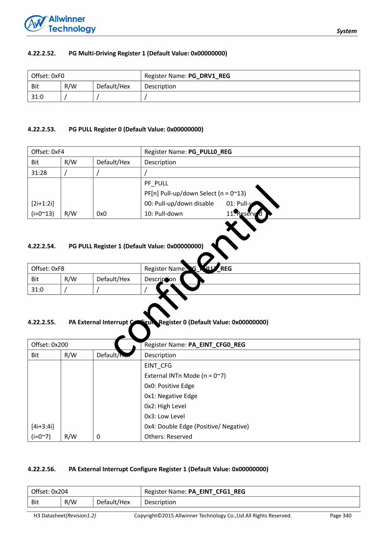
System
H3 Datasheet(Revision1.2) Copyright© 2015 Allwinner Technology Co.,Ltd.All Rights Reserved. Page 340
4.22.2.52. PG Multi-Driving Register 1 (Default Value: 0x00000000)
Offset: 0xF0 Register Name: PG_DRV1_REG
Bit R/W Default/Hex Description
31:0 / / /
4.22.2.53. PG PULL Register 0 (Default Value: 0x00000000)
Offset: 0xF4 Register Name: PG_PULL0_REG
Bit R/W Default/Hex Description
31:28 / / /
[2i+1:2i]
(i=0~13) R/W 0x0
PF_PULL
PF[n] Pull-up/down Select (n = 0~13)
00: Pull-up/down disable 01: Pull-up
10: Pull-down 11: Reserved
4.22.2.54. PG PULL Register 1 (Default Value: 0x00000000)
Offset: 0xF8 Register Name: PG_PULL1_REG
Bit R/W Default/Hex Description
31:0 / / /
4.22.2.55. PA External Interrupt Configure Register 0 (Default Value: 0x00000000)
Offset: 0x200 Register Name: PA_EINT_CFG0_REG
Bit R/W Default/Hex Description
[4i+3:4i]
(i=0~7) R/W 0
EINT_CFG
External INTn Mode (n = 0~7)
0x0: Positive Edge
0x1: Negative Edge
0x2: High Level
0x3: Low Level
0x4: Double Edge (Positive/ Negative)
Others: Reserved
4.22.2.56. PA External Interrupt Configure Register 1 (Default Value: 0x00000000)
Offset: 0x204 Register Name: PA_EINT_CFG1_REG
Bit R/W Default/Hex Description
confid
ential
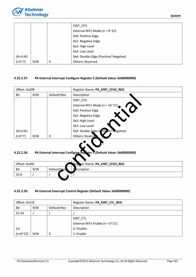
System
H3 Datasheet(Revision1.2) Copyright© 2015 Allwinner Technology Co.,Ltd.All Rights Reserved. Page 341
[4i+3:4i]
(i=0~7) R/W 0
EINT_CFG
External INTn Mode (n = 8~15)
0x0: Positive Edge
0x1: Negative Edge
0x2: High Level
0x3: Low Level
0x4: Double Edge (Positive/ Negative)
Others: Reserved
4.22.2.57. PA External Interrupt Configure Register 2 (Default Value: 0x00000000)
Offset: 0x208 Register Name: PA_EINT_CFG2_REG
Bit R/W Default/Hex Description
[4i+3:4i]
(i=0~7) R/W 0
EINT_CFG
External INTn Mode (n = 16~21)
0x0: Positive Edge
0x1: Negative Edge
0x2: High Level
0x3: Low Level
0x4: Double Edge (Positive/ Negative)
Others: Reserved
4.22.2.58. PA External Interrupt Configure Register 3 (Default Value: 0x00000000)
Offset: 0x20C Register Name: PA_EINT_CFG3_REG
Bit R/W Default/Hex Description
31:0 / / /
4.22.2.59. PA External Interrupt Control Register (Default Value: 0x00000000)
Offset: 0x210 Register Name: PA_EINT_CTL_REG
Bit R/W Default/Hex Description
31:24 / / /
[n]
(n=0~23) R/W 0
EINT_CTL
External INTn Enable (n = 0~21)
0: Disable
1: Enable
confid
ential

System
H3 Datasheet(Revision1.2) Copyright© 2015 Allwinner Technology Co.,Ltd.All Rights Reserved. Page 342
4.22.2.60. PA External Interrupt Status Register (Default Value: 0x00000000)
Offset: 0x214 Register Name: PA_EINT_STATUS_REG
Bit R/W Default/Hex Description
31:24 / / /
[n]
(n=0~23) R/W 0
EINT_STATUS
External INTn Pending Bit (n = 0~21)
0: No IRQ pending
1: IRQ pending
Write ‘1’ to clear
4.22.2.61. PA External Interrupt Debounce Register (Default Value: 0x00000000)
Offset: 0x218 Register Name: PA_EINT_DEB_REG
Bit R/W Default/Hex Description
31:7 / / /
6:4 R/W 0
DEB_CLK_PRE_SCALE
Debounce Clock Pre-scale n
The selected clock source is prescaled by 2^n.
3:1 / / /
0 R/W 0
PIO_INT_CLK_SELECT
PIO Interrupt Clock Select
0: LOSC 32Khz
1: HOSC 24Mhz
4.22.2.62. PG External Interrupt Configure Register 0 (Default Value: 0x00000000)
Offset: 0x220 Register Name: PG_EINT_CFG0_REG
Bit R/W Default/Hex Description
31:12 / / /
[4i+3:4i]
(i=0~7) R/W 0
EINT_CFG
External INTn Mode (n = 0~7)
0x0: Positive Edge
0x1: Negative Edge
0x2: High Level
0x3: Low Level
0x4: Double Edge (Positive/ Negative)
Others: Reserved
confid
ential
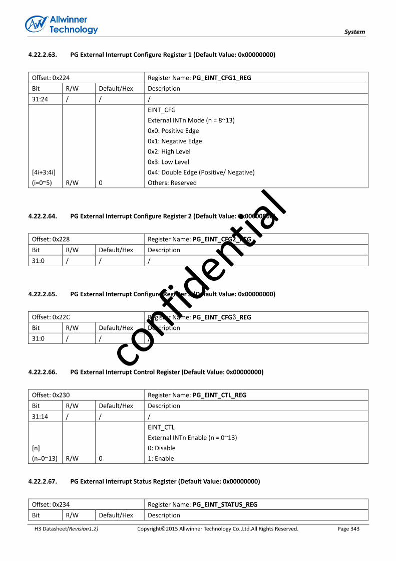
System
H3 Datasheet(Revision1.2) Copyright© 2015 Allwinner Technology Co.,Ltd.All Rights Reserved. Page 343
4.22.2.63. PG External Interrupt Configure Register 1 (Default Value: 0x00000000)
Offset: 0x224 Register Name: PG_EINT_CFG1_REG
Bit R/W Default/Hex Description
31:24 / / /
[4i+3:4i]
(i=0~5) R/W 0
EINT_CFG
External INTn Mode (n = 8~13)
0x0: Positive Edge
0x1: Negative Edge
0x2: High Level
0x3: Low Level
0x4: Double Edge (Positive/ Negative)
Others: Reserved
4.22.2.64. PG External Interrupt Configure Register 2 (Default Value: 0x00000000)
Offset: 0x228 Register Name: PG_EINT_CFG2_REG
Bit R/W Default/Hex Description
31:0 / / /
4.22.2.65. PG External Interrupt Configure Register 3 (Default Value: 0x00000000)
Offset: 0x22C Register Name: PG_EINT_CFG3_REG
Bit R/W Default/Hex Description
31:0 / / /
4.22.2.66. PG External Interrupt Control Register (Default Value: 0x00000000)
Offset: 0x230 Register Name: PG_EINT_CTL_REG
Bit R/W Default/Hex Description
31:14 / / /
[n]
(n=0~13) R/W 0
EINT_CTL
External INTn Enable (n = 0~13)
0: Disable
1: Enable
4.22.2.67. PG External Interrupt Status Register (Default Value: 0x00000000)
Offset: 0x234 Register Name: PG_EINT_STATUS_REG
Bit R/W Default/Hex Description
confid
ential
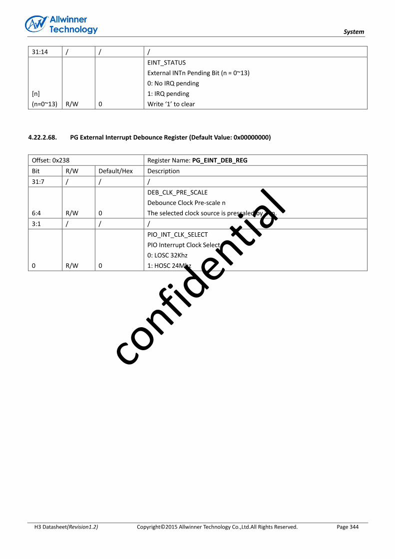
System
H3 Datasheet(Revision1.2) Copyright© 2015 Allwinner Technology Co.,Ltd.All Rights Reserved. Page 344
31:14 / / /
[n]
(n=0~13) R/W 0
EINT_STATUS
External INTn Pending Bit (n = 0~13)
0: No IRQ pending
1: IRQ pending
Write ‘1’ to clear
4.22.2.68. PG External Interrupt Debounce Register (Default Value: 0x00000000)
Offset: 0x238 Register Name: PG_EINT_DEB_REG
Bit R/W Default/Hex Description
31:7 / / /
6:4 R/W 0
DEB_CLK_PRE_SCALE
Debounce Clock Pre-scale n
The selected clock source is prescaled by 2^n.
3:1 / / /
0 R/W 0
PIO_INT_CLK_SELECT
PIO Interrupt Clock Select
0: LOSC 32Khz
1: HOSC 24Mhz
confid
ential
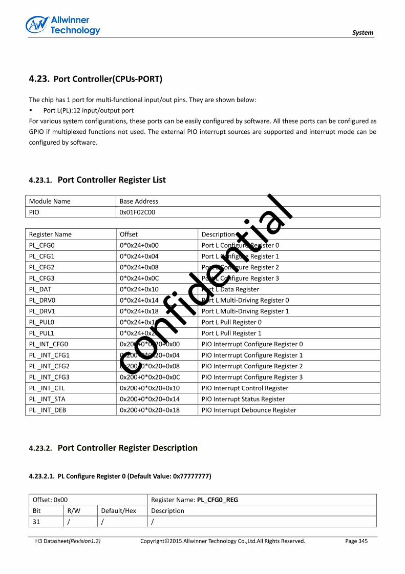
System
H3 Datasheet(Revision1.2) Copyright© 2015 Allwinner Technology Co.,Ltd.All Rights Reserved. Page 345
4.23. Port Controller(CPUs-PORT)
The chip has 1 port for multi-functional input/out pins. They are shown below:
Port L(PL):12 input/output port
For various system configurations, these ports can be easily configured by software. All these ports can be configured as
GPIO if multiplexed functions not used. The external PIO interrupt sources are supported and interrupt mode can be
configured by software.
4.23.1. Port Controller Register List
Module Name Base Address
PIO 0x01F02C00
Register Name Offset Description
PL_CFG0 0*0x24+0x00 Port L Configure Register 0
PL_CFG1 0*0x24+0x04 Port L Configure Register 1
PL_CFG2 0*0x24+0x08 Port L Configure Register 2
PL_CFG3 0*0x24+0x0C Port L Configure Register 3
PL_DAT 0*0x24+0x10 Port L Data Register
PL_DRV0 0*0x24+0x14 Port L Multi-Driving Register 0
PL_DRV1 0*0x24+0x18 Port L Multi-Driving Register 1
PL_PUL0 0*0x24+0x1C Port L Pull Register 0
PL_PUL1 0*0x24+0x20 Port L Pull Register 1
PL_INT_CFG0 0x200+0*0x20+0x00 PIO Interrrupt Configure Register 0
PL _INT_CFG1 0x200+0*0x20+0x04 PIO Interrrupt Configure Register 1
PL _INT_CFG2 0x200+0*0x20+0x08 PIO Interrrupt Configure Register 2
PL _INT_CFG3 0x200+0*0x20+0x0C PIO Interrrupt Configure Register 3
PL _INT_CTL 0x200+0*0x20+0x10 PIO Interrupt Control Register
PL _INT_STA 0x200+0*0x20+0x14 PIO Interrupt Status Register
PL _INT_DEB 0x200+0*0x20+0x18 PIO Interrupt Debounce Register
4.23.2. Port Controller Register Description
4.23.2.1. PL Configure Register 0 (Default Value: 0x77777777)
Offset: 0x00 Register Name: PL_CFG0_REG
Bit R/W Default/Hex Description
31 / / /
confid
ential

System
H3 Datasheet(Revision1.2) Copyright© 2015 Allwinner Technology Co.,Ltd.All Rights Reserved. Page 346
30:28 R/W 0x7
PL7_SELECT
000:Input 001:Output
010:S_JTAG_DI 011:Reserved
100:Reserved 101:Reserved
110:S_PL_EINT7 111:IO Disable
27 / / /
26:24 R/W 0x7
PL6_SELECT
000:Input 001:Output
010:S_JTAG_DO 011:Reserved
100:Reserved 101:Reserved
110:S_PL_EINT6 111:IO Disable
23 / / /
22:20 R/W 0x7
PL5_SELECT
000:Input 001:Output
010:S_JTAG_CK 011:Reserved
100:Reserved 101:Reserved
110:S_PL_EINT5 111:IO Disable
19 / / /
18:16 R/W 0x7
PL4_SELECT
000:Input 001:Output
010:S_JTAG_MS 011:Reserved
100:Reserved 101:Reserved
110:S_PL_EINT4 111:IO Disable
15 / / /
14:12 R/W 0x7
PL3_SELECT
000:Input 001:Output
010:S_UART_RX 011:Reserved
100:Reserved 101:Reserved
110:S_PL_EINT3 111:IO Disable
11 / / /
10:8 R/W 0x7
PL2_SELECT
000:Input 001:Output
010:S_UART_TX 011:Reserved
100:Reserved 101:Reserved
110:S_PL_EINT2 111:IO Disable
7 / / /
6:4 R/W 0x7
PL1_SELECT
000:Input 001:Output
010:S_TWI_SDA 011:Reserved
100:Reserved 101:Reserved
110:S_PL_EINT1 111:IO Disable
3 / / /
2:0 R/W 0x7
PL0_SELECT
000:Input 001:Output
010:S_TWI_SCK 011:Reserved
confid
ential

System
H3 Datasheet(Revision1.2) Copyright© 2015 Allwinner Technology Co.,Ltd.All Rights Reserved. Page 347
100:Reserved 101:Reserved
110:S_PL_EINT0 111:IO Disable
4.23.2.2. PL Configure Register 1 (Default Value: 0x00007777)
Offset: 0x04 Register Name: PL_CFG1_REG
Bit R/W Default/Hex Description
31:15 / / /
14:12 R/W 0x7
PL11_SELECT
000:Input 001:Output
010:S_CIR_RX 011:Reserved
100:Reserved 101:Reserved
110:S_PL_EINT11 111:IO Disable
11 / / /
10:8 R/W 0x7
PL10_SELECT
000:Input 001:Output
010:S_PWM 011:Reserved
100:Reserved 101:Reserved
110:S_PL_EINT10 111:IO Disable
7 / / /
6:4 R/W 0x7
PL9_SELECT
000:Input 001:Output
010:Reserved 011:Reserved
100:Reserved 101:Reserved
110:S_PL_EINT9 111:IO Disable
3 / / /
2:0 R/W 0x7
PL8_SELECT
000:Input 001:Output
010:Reserved 011:Reserved
100:Reserved 101:Reserved
110:S_PL_EINT8 111:IO Disable
4.23.2.3. PL Configure Register 2 (Default Value: 0x00000000)
Offset: 0x08 Register Name: PL_CFG2_REG
Bit R/W Default/Hex Description
31:0 / / /
4.23.2.4. PL Configure Register 3 (Default Value: 0x00000000)
Offset: 0x0C Register Name: PL_CFG3_REG
Bit R/W Default/Hex Description
confid
ential

System
H3 Datasheet(Revision1.2) Copyright© 2015 Allwinner Technology Co.,Ltd.All Rights Reserved. Page 348
31:0 / / /
4.23.2.5. PL Data Register (Default Value: 0x00000000)
Offset: 0x10 Register Name: PL_DATA_REG
Bit R/W Default/Hex Description
31:12 / / /
11:0 R/W 0
PL_DAT
If the port is configured as input, the corresponding bit is the pin state. If
the port is configured as output, the pin state is the same as the
corresponding bit. The read bit value is the value setup by software. If the
port is configured as functional pin, the undefined value will be read.
4.23.2.6. PL Multi-Driving Register 0 (Default Value: 0x00555555)
Offset: 0x14 Register Name: PL_DRV0
Bit R/W Default/Hex Description
31:24 / / /
[2i+1:2i]
(i=0~11) R/W 0x1
PL_DRV
PL[n] Multi-Driving Select (n = 0~11)
00: Level 0 01: Level 1
10: Level 2 11: Level 3
4.23.2.7. PL Multi-Driving Register 1 (Default Value: 0x00000000)
Offset: 0x18 Register Name: PL_DRV1
Bit R/W Default/Hex Description
31:0 / / /
4.23.2.8. PL PULL Register 0 (Default Value: 0x00000005)
Offset: 0x1C Register Name: PL_PULL0
Bit R/W Default/Hex Description
31:24 / / /
[2i+1:2i]
(i=0~11) R/W 0x5
PL_PULL
PL[n] Pull-up/down Select (n = 0~11)
00: Pull-up/down disable 01: Pull-up
10: Pull-down 11: Reserved
confid
ential

System
H3 Datasheet(Revision1.2) Copyright© 2015 Allwinner Technology Co.,Ltd.All Rights Reserved. Page 349
4.23.2.9. PL PULL Register 1 (Default Value: 0x00000000)
Offset: 0x20 Register Name: PL_PULL1
Bit R/W Default/Hex Description
31:0 / / /
4.23.2.10. PL External Interrupt Configure Register 0 (Default Value: 0x00000000)
Offset: 0x200 Register Name: PL_EINT_CFG0
Bit R/W Default/Hex Description
[4i+3:4i]
(i=0~7) R/W 0
EINT_CFG
External INTn Mode (n = 0~7)
0x0: Positive Edge
0x1: Negative Edge
0x2: High Level
0x3: Low Level
0x4: Double Edge (Positive/ Negative)
Others: Reserved
4.23.2.11. PL External Interrupt Configure Register 1 (Default Value: 0x00000000)
Offset: 0x204 Register Name: PL_EINT_CFG1
Bit R/W Default/Hex Description
31:20 / / /
[4i+3:4i]
(i=0~4) R/W 0
EINT_CFG
External INTn Mode (n = 8~11)
0x0: Positive Edge
0x1: Negative Edge
0x2: High Level
0x3: Low Level
0x4: Double Edge (Positive/ Negative)
Others: Reserved
4.23.2.12. PL External Interrupt Configure Register 2 (Default Value: 0x00000000)
Offset: 0x208 Register Name: PL_EINT_CFG2
Bit R/W Default/Hex Description
31:0 / / /
confid
ential

System
H3 Datasheet(Revision1.2) Copyright© 2015 Allwinner Technology Co.,Ltd.All Rights Reserved. Page 350
4.23.2.13. PL External Interrupt Configure Register 3 (Default Value: 0x00000000)
Offset: 0x20C Register Name: PL_EINT_CFG3
Bit R/W Default/Hex Description
31:0 / / /
4.23.2.14. PL External Interrupt Control Register (Default Value: 0x00000000)
Offset: 0x210 Register Name: PL_EINT_CTL
Bit R/W Default/Hex Description
31:12 / / /
[n]
(n=0~11) R/W 0
EINT_CTL
External INTn Enable (n = 0~11)
0: Disable
1: Enable
4.23.2.15. PL External Interrupt Status Register (Default Value: 0x00000000)
Offset: 0x214 Register Name: PL_EINT_STATUS
Bit R/W Default/Hex Description
31:12 / / /
[n]
(n=0~11) R/W 0
EINT_STATUS
External INTn Pending Bit (n = 0~11)
0: No IRQ pending
1: IRQ pending
Write ‘1’ to clear
4.23.2.16. PL External Interrupt Debounce Register (Default Value: 0x00000000)
Offset: 0x218 Register Name: PL_EINT_DEB
Bit R/W Default/Hex Description
31:7 / / /
6:4 R/W 0
DEB_CLK_PRE_SCALE
Debounce Clock Pre-scale n
The selected clock source is prescaled by 2^n.
3:1 / / /
0 R/W 0
PIO_INT_CLK_SELECT
PIO Interrupt Clock Select
0: LOSC 32KHz
1: HOSC 24MHz
confid
ential

Memory
H3 Datasheet(Revision1.2) Copyright© 2015 Allwinner Technology Co.,Ltd.All Rights Reserved. Page 351
Chapter 5 Memory
This section describes the H3 memory from three aspects:
SDRAM
NAND Flash
SD/MMC
5.1. SDRAM
5.1.1. Overview
The SDRAM Controller (DRAMC) provides a simple, flexible, burst-optimized interface to all industy-standard SDRAM. It
supports up to a 16G bits memory address space.
The DRAMC automatically handles memory management, initialization, and refresh operations. It gives the host CPU a
simple command interface, hiding details of the required address, page, and burst handling procedures. All memory
parameters are runtime-configurable, including timing, memory setting, SDRAM type, and Extended-Mode-Register
settings. To simplify chip system integration, DDR controller works in half rate mode.
The DRAMC includes the following features:
Support 32-bits one channel
Support 2 Chip Select
Support DDR2/DDR3/DDR3L/LPDDR2/LPDDR3 SDRAM
Support Different Memory Device’s Power Voltage of 1.2V 1.35V 1.5V and 1.8V
Support clock frequency up to 667 MHz(DDR3-1333)
Support Memory Capacity up to 16G bits (2G Bytes)
Support 16 address lines and three bank address lines per channel
Automatically generates initialization and refresh sequences
Runtime-configurable parameters setting for application flexibility
Priority of transferring through multiple ports is programmable
Random read or write operation is supported
confid
ential

Memory
H3 Datasheet(Revision1.2) Copyright© 2015 Allwinner Technology Co.,Ltd.All Rights Reserved. Page 352
5.2. NAND Flash
5.2.1. Overview
The NDFC is the NAND Flash Controller which supports all NAND flash memory available in the market. New type flash
can be supported by software re-configuration.
The On-the-fly error correction code (ECC) is built-in NDFC for enhancing reliability. BCH is implemented and it can
detect and correct up to 64 bits error per 512 or 1024 bytes data. The on chip ECC and parity checking circuitry of NDFC
frees CPU for other tasks. The ECC function can be disabled by software.
The data can be transferred by DMA or by CPU memory-mapped IO method. The NDFC provides automatic timing
control for reading or writing external Flash. The NDFC maintains the proper relativity for CLE, CE# and ALE control
signal lines. Three modes are supported for serial read access. The conventional serial access is mode 0 and mode 1 is
for EDO type and mode 2 for extension EDO type. NDFC can monitor the status of R/B# signal line.
Block management and wear leveling management are implemented in software.
The NAND Flash Controller (NDFC) includes the following features:
Supports all SLC/MLC/TLC flash and EF-NAND memory available in the market
Software configure seed for randomize engine
Software configure method for adaptability to a variety of system and memory types
Supports 8-bit Data Bus Width
Supports 1024, 2048, 4096, 8192, 16384 bytes size per page
Supports Conventional and EDO serial access method for serial reading Flash
On-the-fly BCH error correction code which correcting up to 64 bits per 512 or 1024 bytes
Corrected Error bits number information report
ECC automatic disable function for all 0xff data
NDFC status information is reported by its’ registers and interrupt is supported
One Command FIFO
External DMA is supported for transferring data
Two 256x32-bit RAM for Pipeline Procession
Support SDR, ONFI DDR and Toggle DDR NAND
Support self–debug for NDFC debug
5.2.2. Block Diagram
The NAND Flash Controller (NDFC) system block diagram is shown below:
confid
ential

Memory
H3 Datasheet(Revision1.2) Copyright© 2015 Allwinner Technology Co.,Ltd.All Rights Reserved. Page 353
Sync
Register
File
FIFO
RAM0
(256x32)
ECC
Control
AHB
Slave I/F
Command
FIFO
FIFO
Control
DMA & INT
Control
FIFO
RAM1
(256x32)
NAND Flash Basic Operation
Normal
Command
FSM
Spare
Command
FSM
Batch
Command
FSM
User Data
(8x32)
CE[7:0] CLE ALE WE RE RB[1:0] DO[7:0] DI[7:0]
nfc_clk
domain
ahb_clk
domain
Figure 5-1. NDFC Block Diagram
5.2.3. NDFC Timing Diagram
Typically, there are two kinds of serial access method. One method is conventional method which fetching data at the
rise edge of NDFC_RE# signal line. Another one is EDO type which fetching data at the next fall edge of NDFC_RE# signal
line.
confid
ential

Memory
H3 Datasheet(Revision1.2) Copyright© 2015 Allwinner Technology Co.,Ltd.All Rights Reserved. Page 354
NDFC_CLE
NDFC_CE#
NDFC_WE#
NDFC_RE#
NDFC_RB#
NDFC_ALE
NDFC_IOx
t3
t10
t12t14
t13
t4
sample 0 sample n-1
D(0) D(n-1)
Figure 5-2. Conventional Serial Access Cycle Diagram (SAM0)
t3
t10
t12t14
t13
t4
sample 0
D(0) D(n-1)
NDFC_CLE
NDFC_CE#
NDFC_WE#
NDFC_RE#
NDFC_RB#
NDFC_ALE
NDFC_IOx
Figure 5-3. EDO type Serial Access after Read Cycle (SAM1)
confid
ential

Memory
H3 Datasheet(Revision1.2) Copyright© 2015 Allwinner Technology Co.,Ltd.All Rights Reserved. Page 355
t3
t10
t14t12
t13
sample 0
D(0) D(n-1)
NDFC_CLE
NDFC_CE#
NDFC_WE#
NDFC_RE#
NDFC_RB#
NDFC_ALE
NDFC_IOx
Figure 5-4. Extending EDO type Serial Access Mode (SAM2)
t1
t5
t11
t4
t2
t3
t7
t8 t9
COMMAND
NDFC_CLE
NDFC_CE#
NDFC_WE#
NDFC_RE#
NDFC_ALE
NDFC_IOx
Figure 5-5. Command Latch Cycle
confid
ential

Memory
H3 Datasheet(Revision1.2) Copyright© 2015 Allwinner Technology Co.,Ltd.All Rights Reserved. Page 356
t5
t6t15
t1
t3
t7
t8 t9
t4
t11
Addr(0) Addr(n-1)
NDFC_CLE
NDFC_CE#
NDFC_WE#
NDFC_RE#
NDFC_ALE
NDFC_IOx
Figure 5-6. Address Latch Cycle
t5
t6t15
t1
t3
t7
t8 t9
t4
t11
D(0) D(n-1)
NDFC_CLE
NDFC_CE#
NDFC_WE#
NDFC_RE#
NDFC_ALE
NDFC_IOx
Figure 5-7. Write Data to Flash Cycle
confid
ential

Memory
H3 Datasheet(Revision1.2) Copyright© 2015 Allwinner Technology Co.,Ltd.All Rights Reserved. Page 357
D(0)CMD D(n-1)
NDFC_CLE
NDFC_CE#
NDFC_WE#
NDFC_RE
NDFC_ALE
NDFC_RB#
NDFC_IOx
t16
t14t12 t13
Figure 5-8. Waiting R/B# ready Diagram
D(0)CMD D(n-1)
NDFC_CLE
NDFC_CE#
NDFC_WE#
NDFC_RE
NDFC_ALE
NDFC_RB#
NDFC_IOx
t17
Figure 5-9. WE# high to RE# low Timing Diagram
confid
ential

Memory
H3 Datasheet(Revision1.2) Copyright© 2015 Allwinner Technology Co.,Ltd.All Rights Reserved. Page 358
D(n-1) 05hD(n-2) Col1 Col2
NDFC_CLE
NDFC_CE#
NDFC_WE#
NDFC_RE
NDFC_ALE
NDFC_RB#
NDFC_IOx
t18
Figure 5-10. RE# high to WE# low Timing Diagram
Addr3 D(0)Addr2 D(1) D(2)
NDFC_CLE
NDFC_CE#
NDFC_WE#
NDFC_RE
NDFC_ALE
NDFC_RB#
NDFC_IOx
t19
Figure 5-11. Address to Data Loading Timing Diagram
Timing cycle list:
confid
ential
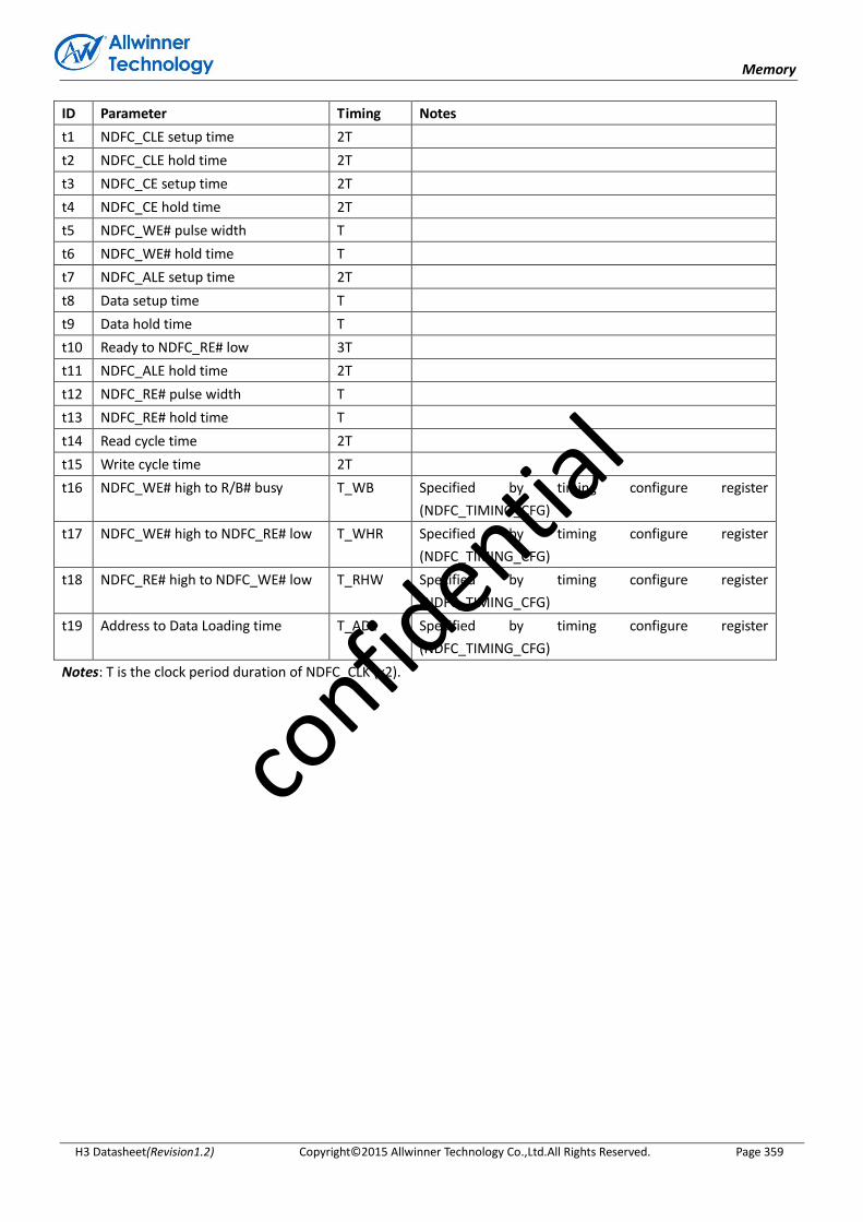
Memory
H3 Datasheet(Revision1.2) Copyright© 2015 Allwinner Technology Co.,Ltd.All Rights Reserved. Page 359
ID Parameter Timing Notes
t1 NDFC_CLE setup time 2T
t2 NDFC_CLE hold time 2T
t3 NDFC_CE setup time 2T
t4 NDFC_CE hold time 2T
t5 NDFC_WE# pulse width T
t6 NDFC_WE# hold time T
t7 NDFC_ALE setup time 2T
t8 Data setup time T
t9 Data hold time T
t10 Ready to NDFC_RE# low 3T
t11 NDFC_ALE hold time 2T
t12 NDFC_RE# pulse width T
t13 NDFC_RE# hold time T
t14 Read cycle time 2T
t15 Write cycle time 2T
t16 NDFC_WE# high to R/B# busy T_WB Specified by timing configure register
(NDFC_TIMING_CFG)
t17 NDFC_WE# high to NDFC_RE# low T_WHR Specified by timing configure register
(NDFC_TIMING_CFG)
t18 NDFC_RE# high to NDFC_WE# low T_RHW Specified by timing configure register
(NDFC_TIMING_CFG)
t19 Address to Data Loading time T_ADL Specified by timing configure register
(NDFC_TIMING_CFG)
Notes: T is the clock period duration of NDFC_CLK (x2).
confid
ential

Memory
H3 Datasheet(Revision1.2) Copyright© 2015 Allwinner Technology Co.,Ltd.All Rights Reserved. Page 360
5.2.4. NDFC Operation Guide
NDFC_CLE
NDFC_CE#
NDFC_WE#
NDFC_RE
NDFC_ALE
NDFC_RB#
NDFC_IOx 00h Addr(5 cycle) 30h Data output
First Command
cmdio[22]
cmdio[7:0]
Address Cycle
cmdio[18:16]
cmdio[19]=1
Second Command
cmdio[24]
Wait RB Signal
cmdio[23]
Sequence Read
cmdio[20]=0
cmdio[25]=1
Page Command
cmdio[31:30]=2
Figure 5-12. Page Read Command Diagram
NDFC_CLE
NDFC_CE#
NDFC_WE#
NDFC_RE
NDFC_ALE
NDFC_RB#
NDFC_IOx 80h Addr(5 cycle) Data Input
First Command
cmdio[22]
cmdio[7:0]
Address Cycle
cmdio[18:16]
cmdio[19]=1
Sequence Write
cmdio[20]=1
cmdio[25]=1
Page Command
cmdio[31:30]=2
Wait RB Signal
cmdio[23]
Figure 5-13. Page Program Diagram
confid
ential

Memory
H3 Datasheet(Revision1.2) Copyright© 2015 Allwinner Technology Co.,Ltd.All Rights Reserved. Page 361
NDFC_CLE
NDFC_CE#
NDFC_WE#
NDFC_RE
NDFC_ALE
NDFC_RB#
NDFC_IOx 00h 30h
First Command
cmdio[22]
cmdio[7:0]
Address Cycle
cmdio[18:16]
cmdio[19]=1
Second Command
cmdio[24]
Wait RB Signal
cmdio[23]
Page Command
cmdio[31:30]=2
col0 col1 row0row1row2 70h d(0) 00h Data output
Third Comand
cmdio[28]
Forth Comand
cmdio[29]
Sequence Read
cmdio[20]=0
cmdio[25]=1
Figure 5-14. EF-NAND Page Read Diagram
NDFC_CLE
NDFC_CE#
NDFC_WE#
NDFC_RE
NDFC_ALE
NDFC_RB#
NDFC_IOx 00h 30h Data output
First Command
cmdio[22]
cmdio[7:0]
Address Cycle
cmdio[18:16]
cmdio[19]=1
Second Command
cmdio[24]
Wait RB Signal
cmdio[23]
Interleave Read
cmdio[20]=0
cmdio[25]=0
Page Command
cmdio[31:30]=2
col0 col1 row0row1row2 05h col0 col1 E0h Data output
Address set by hardware
automatically
Figure 5-15. Interleave Page Read Diagram
5.2.5. NDFC Register List
Module Name Base Address
NDFC 0x01C03000
Register Name Offset Description
NDFC_CTL 0x00 NDFC Configure and Control Register
NDFC_ST 0x04 NDFC Status Information Register
NDFC_INT 0x08 NDFC Interrupt Control Register
NDFC_TIMING_CTL 0x0C NDFC Timing Control Register
confid
ential
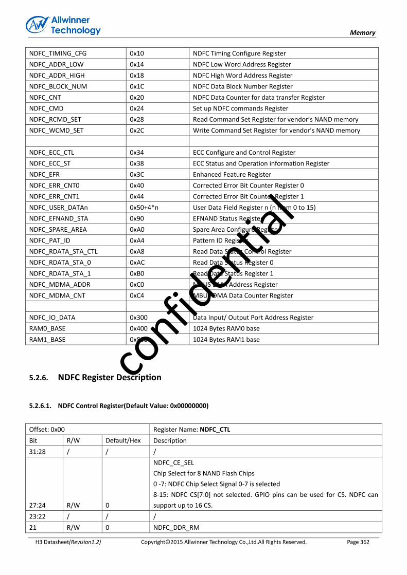
Memory
H3 Datasheet(Revision1.2) Copyright© 2015 Allwinner Technology Co.,Ltd.All Rights Reserved. Page 362
NDFC_TIMING_CFG 0x10 NDFC Timing Configure Register
NDFC_ADDR_LOW 0x14 NDFC Low Word Address Register
NDFC_ADDR_HIGH 0x18 NDFC High Word Address Register
NDFC_BLOCK_NUM 0x1C NDFC Data Block Number Register
NDFC_CNT 0x20 NDFC Data Counter for data transfer Register
NDFC_CMD 0x24 Set up NDFC commands Register
NDFC_RCMD_SET 0x28 Read Command Set Register for vendor’s NAND memory
NDFC_WCMD_SET 0x2C Write Command Set Register for vendor’s NAND memory
NDFC_ECC_CTL 0x34 ECC Configure and Control Register
NDFC_ECC_ST 0x38 ECC Status and Operation information Register
NDFC_EFR 0x3C Enhanced Feature Register
NDFC_ERR_CNT0 0x40 Corrected Error Bit Counter Register 0
NDFC_ERR_CNT1 0x44 Corrected Error Bit Counter Register 1
NDFC_USER_DATAn 0x50+4*n User Data Field Register n (n from 0 to 15)
NDFC_EFNAND_STA 0x90 EFNAND Status Register
NDFC_SPARE_AREA 0xA0 Spare Area Configure Register
NDFC_PAT_ID 0xA4 Pattern ID Register
NDFC_RDATA_STA_CTL 0xA8 Read Data Status Control Register
NDFC_RDATA_STA_0 0xAC Read Data Status Register 0
NDFC_RDATA_STA_1 0xB0 Read Data Status Register 1
NDFC_MDMA_ADDR 0xC0 MBUS DMA Address Register
NDFC_MDMA_CNT 0xC4 MBUS DMA Data Counter Register
NDFC_IO_DATA 0x300 Data Input/ Output Port Address Register
RAM0_BASE 0x400 1024 Bytes RAM0 base
RAM1_BASE 0x800 1024 Bytes RAM1 base
5.2.6. NDFC Register Description
5.2.6.1. NDFC Control Register(Default Value: 0x00000000)
Offset: 0x00 Register Name: NDFC_CTL
Bit R/W Default/Hex Description
31:28 / / /
27:24 R/W 0
NDFC_CE_SEL
Chip Select for 8 NAND Flash Chips
0 -7: NDFC Chip Select Signal 0-7 is selected
8-15: NDFC CS[7:0] not selected. GPIO pins can be used for CS. NDFC can
support up to 16 CS.
23:22 / / /
21 R/W 0 NDFC_DDR_RM
confid
ential

Memory
H3 Datasheet(Revision1.2) Copyright© 2015 Allwinner Technology Co.,Ltd.All Rights Reserved. Page 363
DDR Repeat data mode
0: Lower byte
1: Higher byte
20 R/W 0
NDFC_DDR_REN
DDR Repeat Enable
0: Disable
1: Enable
19:18 R/W 0
NF_TYPE
NAND Flash Type
0x0: Normal SDR NAND
0x1: Reserved
0x2: ONFI DDR NAND
0x3: Toggle DDR NAND
17 R/W 0
NDFC_CLE_POL
NDFC Command Latch Enable (CLE) Signal Polarity Select
0: High active
1: Low active
16 R/W 0
NDFC_ALE_POL
NDFC Address Latch Enable (ALE) Signal Polarity Select
0: High active
1: Low active
15 R/W 0
NDFC_DMA_TYPE
0: Dedicated DMA
1: Normal DMA
14 R/W 0
NDFC_RAM_METHOD
Access internal RAM method
0: Access internal RAM by AHB bus
1: Access internal RAM by DMA bus
13:12 / / /
11:8 R/W 0x0
NDFC_PAGE_SIZE
0x0: 1024 bytes
0x1: 2048 bytes
0x2: 4096 bytes
0x3: 8192 bytes
0x4: 16384 bytes
Notes: The page size is for main field data.
7 / / /
6 R/W 0
NDFC_CE_ACT
Chip Select Signal CE# Control During NAND operation
0: De-active Chip Select Signal NDFC_CE# during data loading, serial access
and other no operation stage for power consumption. NDFC automatic
control Chip Select Signals.
1: Chip select signal NDFC_CE# is always active after NDFC is enabled
5 / / /
4:3 R/W 0 NDFC_RB_SEL
confid
ential
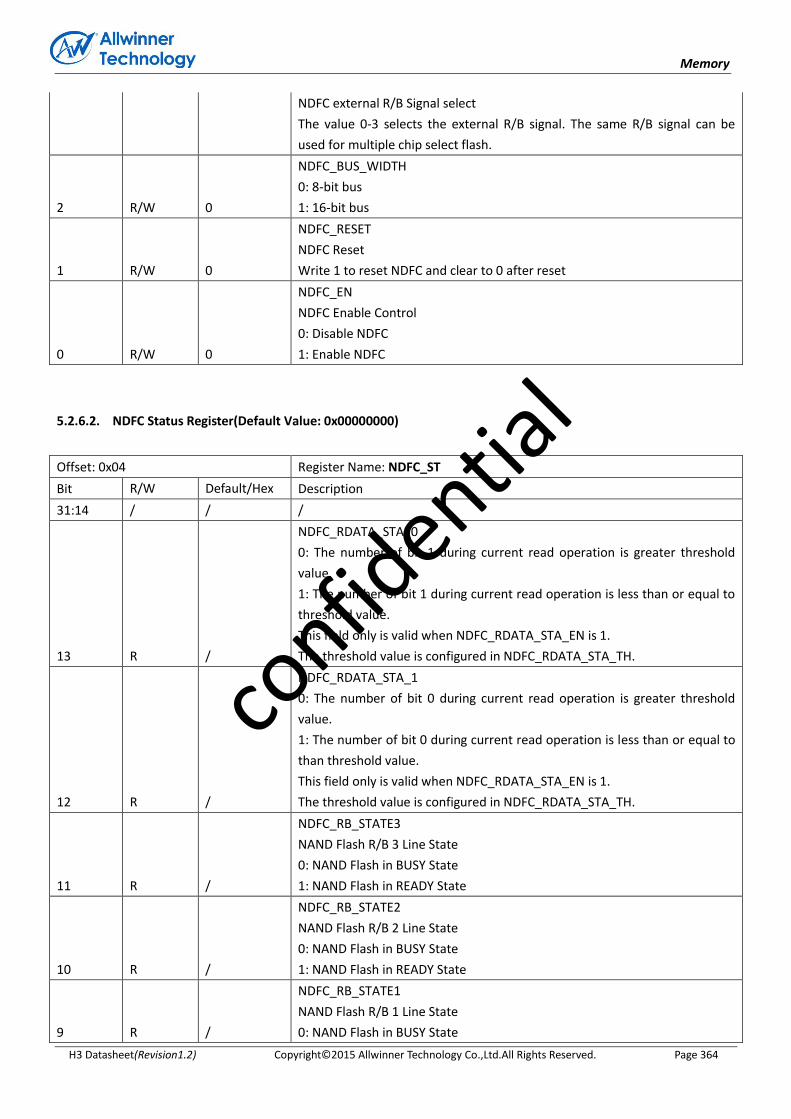
Memory
H3 Datasheet(Revision1.2) Copyright© 2015 Allwinner Technology Co.,Ltd.All Rights Reserved. Page 364
NDFC external R/B Signal select
The value 0-3 selects the external R/B signal. The same R/B signal can be
used for multiple chip select flash.
2 R/W 0
NDFC_BUS_WIDTH
0: 8-bit bus
1: 16-bit bus
1 R/W 0
NDFC_RESET
NDFC Reset
Write 1 to reset NDFC and clear to 0 after reset
0 R/W 0
NDFC_EN
NDFC Enable Control
0: Disable NDFC
1: Enable NDFC
5.2.6.2. NDFC Status Register(Default Value: 0x00000000)
Offset: 0x04 Register Name: NDFC_ST
Bit R/W Default/Hex Description
31:14 / / /
13 R /
NDFC_RDATA_STA_0
0: The number of bit 1 during current read operation is greater threshold
value.
1: The number of bit 1 during current read operation is less than or equal to
threshold value.
This field only is valid when NDFC_RDATA_STA_EN is 1.
The threshold value is configured in NDFC_RDATA_STA_TH.
12 R /
NDFC_RDATA_STA_1
0: The number of bit 0 during current read operation is greater threshold
value.
1: The number of bit 0 during current read operation is less than or equal to
than threshold value.
This field only is valid when NDFC_RDATA_STA_EN is 1.
The threshold value is configured in NDFC_RDATA_STA_TH.
11 R /
NDFC_RB_STATE3
NAND Flash R/B 3 Line State
0: NAND Flash in BUSY State
1: NAND Flash in READY State
10 R /
NDFC_RB_STATE2
NAND Flash R/B 2 Line State
0: NAND Flash in BUSY State
1: NAND Flash in READY State
9 R /
NDFC_RB_STATE1
NAND Flash R/B 1 Line State
0: NAND Flash in BUSY State
confid
ential
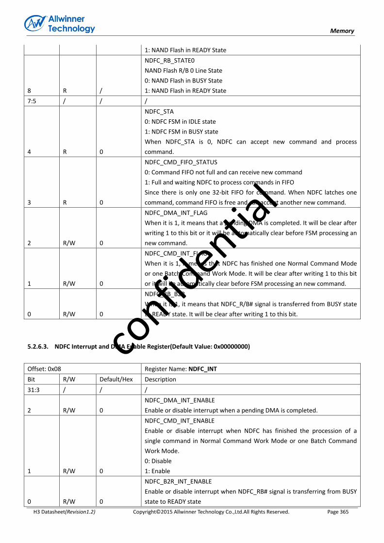
Memory
H3 Datasheet(Revision1.2) Copyright© 2015 Allwinner Technology Co.,Ltd.All Rights Reserved. Page 365
1: NAND Flash in READY State
8 R /
NDFC_RB_STATE0
NAND Flash R/B 0 Line State
0: NAND Flash in BUSY State
1: NAND Flash in READY State
7:5 / / /
4 R 0
NDFC_STA
0: NDFC FSM in IDLE state
1: NDFC FSM in BUSY state
When NDFC_STA is 0, NDFC can accept new command and process
command.
3 R 0
NDFC_CMD_FIFO_STATUS
0: Command FIFO not full and can receive new command
1: Full and waiting NDFC to process commands in FIFO
Since there is only one 32-bit FIFO for command. When NDFC latches one
command, command FIFO is free and can accept another new command.
2 R/W 0
NDFC_DMA_INT_FLAG
When it is 1, it means that a pending DMA is completed. It will be clear after
writing 1 to this bit or it will be automatically clear before FSM processing an
new command.
1 R/W 0
NDFC_CMD_INT_FLAG
When it is 1, it means that NDFC has finished one Normal Command Mode
or one Batch Command Work Mode. It will be clear after writing 1 to this bit
or it will be automatically clear before FSM processing an new command.
0 R/W 0
NDFC_RB_B2R
When it is 1, it means that NDFC_R/B# signal is transferred from BUSY state
to READY state. It will be clear after writing 1 to this bit.
5.2.6.3. NDFC Interrupt and DMA Enable Register(Default Value: 0x00000000)
Offset: 0x08 Register Name: NDFC_INT
Bit R/W Default/Hex Description
31:3 / / /
2 R/W 0
NDFC_DMA_INT_ENABLE
Enable or disable interrupt when a pending DMA is completed.
1 R/W 0
NDFC_CMD_INT_ENABLE
Enable or disable interrupt when NDFC has finished the procession of a
single command in Normal Command Work Mode or one Batch Command
Work Mode.
0: Disable
1: Enable
0 R/W 0
NDFC_B2R_INT_ENABLE
Enable or disable interrupt when NDFC_RB# signal is transferring from BUSY
state to READY state
confid
ential
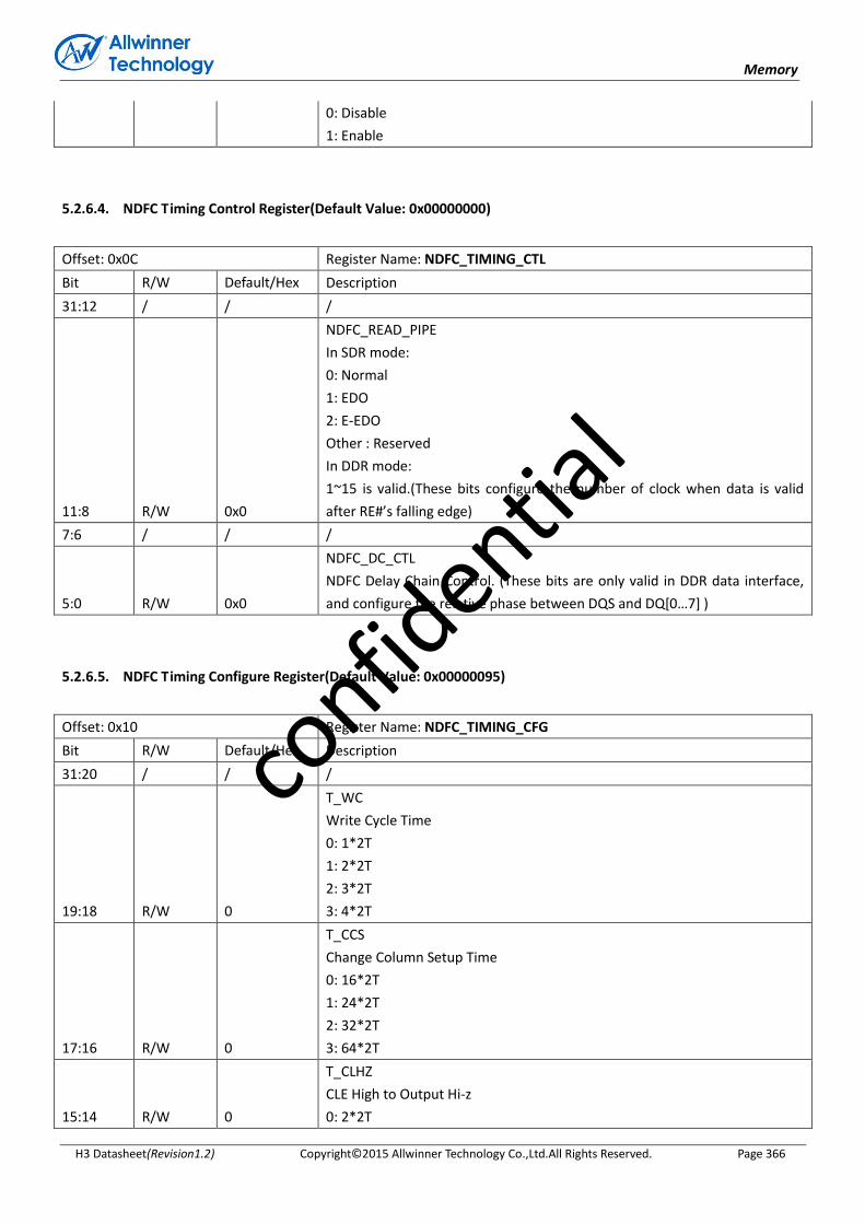
Memory
H3 Datasheet(Revision1.2) Copyright© 2015 Allwinner Technology Co.,Ltd.All Rights Reserved. Page 366
0: Disable
1: Enable
5.2.6.4. NDFC Timing Control Register(Default Value: 0x00000000)
Offset: 0x0C Register Name: NDFC_TIMING_CTL
Bit R/W Default/Hex Description
31:12 / / /
11:8 R/W 0x0
NDFC_READ_PIPE
In SDR mode:
0: Normal
1: EDO
2: E-EDO
Other : Reserved
In DDR mode:
1~15 is valid.(These bits configure the number of clock when data is valid
after RE#’s falling edge)
7:6 / / /
5:0 R/W 0x0
NDFC_DC_CTL
NDFC Delay Chain Control. (These bits are only valid in DDR data interface,
and configure the relative phase between DQS and DQ[0…7] )
5.2.6.5. NDFC Timing Configure Register(Default Value: 0x00000095)
Offset: 0x10 Register Name: NDFC_TIMING_CFG
Bit R/W Default/Hex Description
31:20 / / /
19:18 R/W 0
T_WC
Write Cycle Time
0: 1*2T
1: 2*2T
2: 3*2T
3: 4*2T
17:16 R/W 0
T_CCS
Change Column Setup Time
0: 16*2T
1: 24*2T
2: 32*2T
3: 64*2T
15:14 R/W 0
T_CLHZ
CLE High to Output Hi-z
0: 2*2T
confid
ential
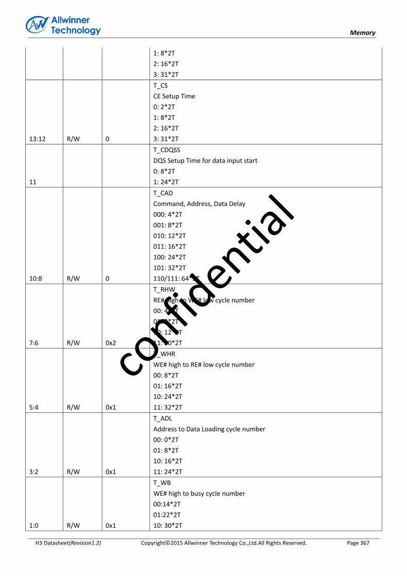
Memory
H3 Datasheet(Revision1.2) Copyright© 2015 Allwinner Technology Co.,Ltd.All Rights Reserved. Page 367
1: 8*2T
2: 16*2T
3: 31*2T
13:12 R/W 0
T_CS
CE Setup Time
0: 2*2T
1: 8*2T
2: 16*2T
3: 31*2T
11
T_CDQSS
DQS Setup Time for data input start
0: 8*2T
1: 24*2T
10:8 R/W 0
T_CAD
Command, Address, Data Delay
000: 4*2T
001: 8*2T
010: 12*2T
011: 16*2T
100: 24*2T
101: 32*2T
110/111: 64*2T
7:6 R/W 0x2
T_RHW
RE# high to WE# low cycle number
00: 4*2T
01: 8*2T
10: 12*2T
11: 20*2T
5:4 R/W 0x1
T_WHR
WE# high to RE# low cycle number
00: 8*2T
01: 16*2T
10: 24*2T
11: 32*2T
3:2 R/W 0x1
T_ADL
Address to Data Loading cycle number
00: 0*2T
01: 8*2T
10: 16*2T
11: 24*2T
1:0 R/W 0x1
T_WB
WE# high to busy cycle number
00:14*2T
01:22*2T
10: 30*2T
confid
ential
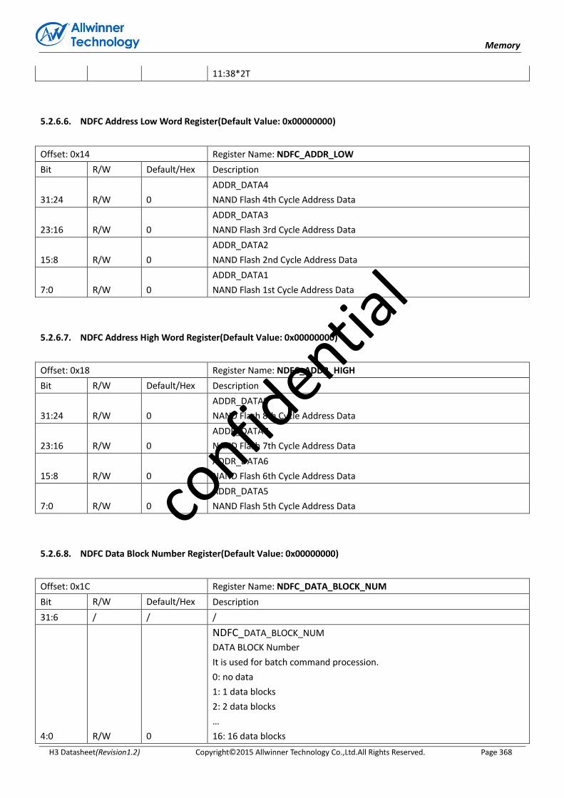
Memory
H3 Datasheet(Revision1.2) Copyright© 2015 Allwinner Technology Co.,Ltd.All Rights Reserved. Page 368
11:38*2T
5.2.6.6. NDFC Address Low Word Register(Default Value: 0x00000000)
Offset: 0x14 Register Name: NDFC_ADDR_LOW
Bit R/W Default/Hex Description
31:24 R/W 0
ADDR_DATA4
NAND Flash 4th Cycle Address Data
23:16 R/W 0
ADDR_DATA3
NAND Flash 3rd Cycle Address Data
15:8 R/W 0
ADDR_DATA2
NAND Flash 2nd Cycle Address Data
7:0 R/W 0
ADDR_DATA1
NAND Flash 1st Cycle Address Data
5.2.6.7. NDFC Address High Word Register(Default Value: 0x00000000)
Offset: 0x18 Register Name: NDFC_ADDR_HIGH
Bit R/W Default/Hex Description
31:24 R/W 0
ADDR_DATA8
NAND Flash 8th Cycle Address Data
23:16 R/W 0
ADDR_DATA7
NAND Flash 7th Cycle Address Data
15:8 R/W 0
ADDR_DATA6
NAND Flash 6th Cycle Address Data
7:0 R/W 0
ADDR_DATA5
NAND Flash 5th Cycle Address Data
5.2.6.8. NDFC Data Block Number Register(Default Value: 0x00000000)
Offset: 0x1C Register Name: NDFC_DATA_BLOCK_NUM
Bit R/W Default/Hex Description
31:6 / / /
4:0 R/W 0
NDFC_DATA_BLOCK_NUM
DATA BLOCK Number
It is used for batch command procession.
0: no data
1: 1 data blocks
2: 2 data blocks
…
16: 16 data blocks
confid
ential

Memory
H3 Datasheet(Revision1.2) Copyright© 2015 Allwinner Technology Co.,Ltd.All Rights Reserved. Page 369
Others: Reserved
Notes: 1 data block = 512 or 1024 bytes main field data
5.2.6.9. NDFC Data Counter Register(Default Value: 0x00000000)
Offset: 0x20 Register Name: NDFC_CNT
Bit R/W Default/Hex Description
31:10 / / /
9:0 R/W 0
NDFC_DATA_CNT
Transfer Data Byte Counter
The length can be set from 1 byte to 1024 bytes. However, 1024 bytes is set
when it is zero.
5.2.6.10. NDFC Command IO Register(Default Value: 0x00000000)
Offset: 0x24 Register Name: NDFC_CMD
Bit R/W Default/Hex Description
31:30 R/W 0
NDFC_CMD_TYPE
00: Common Command for normal operation
01: Special Command for Flash Spare Field Operation
10: Page Command for batch process operation
11: Reserved
29 R/W 0
NDFC_SEND_FOURTH_CMD
0: Don’t send third set command
1: Send it on the external memory’s bus
Notes:It is used for EF-NAND page read.
28 R/W 0
NDFC_SEND_THIRD_CMD
0: Don’t send third set command
1: Send it on the external memory’s bus
Notes:It is used for EF-NAND page read.
27 R/W 0
NDFC_ROW_ADDR_AUTO
Row Address Auto Increase for Page Command
0: Normal operation
1: Row address increasing automatically
26 R/W 0
NDFC_DATA_METHOD
Data swap method when the internal RAM and system memory
It is only active for Common Command and Special Command.
0: No action
1: DMA transfer automatically
It only is active when NDFC_RAM_METHOD is 1.
If this bit is set to 1, NDFC should setup DRQ to fetching data before output
to Flash or NDFC should setup DRQ to sending out to system memory after
confid
ential

Memory
H3 Datasheet(Revision1.2) Copyright© 2015 Allwinner Technology Co.,Ltd.All Rights Reserved. Page 370
fetching data from Flash.
If this bit is set to 0, NDFC output the data in internal RAM or do nothing
after fetching data from Flash.
25 R/W 0
NDFC_SEQ
User data & BCH check word position. It only is active for Page Command,
don’t care about this bit for other two commands
0: Interleave Method (on page spare area)
1: Sequence Method (following data block)
24 R/W 0
NDFC_SEND_SECOND_CMD
0: Don’t send second set command
1: Send it on the external memory’s bus
23 R/W 0
NDFC_WAIT_FLAG
0: NDFC can transfer data regardless of the internal NDFC_RB wire
1: NDFC can transfer data when the internal NDFC_RB wire is READY;
otherwise it can’t when the internal NDFC_RB wire is BUSY.
22 R/W 0
NDFC_SEND_FIRST_CMD
0: Don’t send first set command
1: Send it on the external memory’s bus
21 R/W 0
NDFC_DATA_TRANS
0: No data transfer on external memory bus
1: Data transfer and direction is decided by the field NDFC_ACCESS_DIR
20 R/W 0
NDFC_ACCESS_DIR
0: Read NAND Flash
1: Write NAND Flash
19 R/W 0
NDFC_SEND_ADR
0: Don’t send ADDRESS
1: Send N cycles ADDRESS, the number N is specified by NDFC_ADR_NUM
field
18:16 R/W 0
NDFC_ADR_NUM
Address Cycles’ Number
000: 1 cycle address field
001: 2 cycles address field
010: 3 cycles address field
011: 4 cycles address field
100: 5 cycles address field
101: 6 cycles address field
110: 7 cycles address field
111: 8 cycles address field
15:8 R/W 0
NDFC_CMD_HIGH_BYTE
NDFC Command high byte data
If 8-bit command is supported, the high byte should be zero for 16-bit bus
width NAND Flash. For 8-bit bus width NAND Flash, high byte command is
discarded.
7:0 R/W 0
NDFC_CMD_LOW_BYTE
NDFC Command low byte data
confid
ential

Memory
H3 Datasheet(Revision1.2) Copyright© 2015 Allwinner Technology Co.,Ltd.All Rights Reserved. Page 371
This command will be sent to external Flash by NDFC.
5.2.6.11. NDFC Command Set Register 0(Default Value: 0x00E00530)
Offset: 0x28 Register Name: NDFC_CMD_SET0
Bit R/W Default/Hex Description
31:24 / / /
23:16 R/W 0xE0
NDFC_RANDOM_READ_CMD1
Used for Batch Read Operation
15:8 R/W 0x05
NDFC_RANDOM_READ_CMD0
Used for Batch Read Operation
7:0 R/W 0x30
NDFC_READ_CMD
Used for Batch Read Operation
5.2.6.12. NDFC Command Set Register 1(Default Value: 0x70008510)
Offset: 0x2C Register Name: NDFC_CMD_SET1
Bit R/W Default/Hex Description
31:16 R/W 0x70
NDFC_READ_CMD0
Used for EF-NAND Page Read operation
23:16 R/W 0x00
NDFC_READ_CMD1
Used for EF-NAND Page Read operation
15:8 R/W 0x85
NDFC_RANDOM_WRITE_CMD
Used for Batch Write Operation
7:0 R/W 0x10
NDFC_PROGRAM_CMD
Used for Batch Write Operation
5.2.6.13. NDFC IO Data Register(Default Value: 0x00000000)
Offset: 0x30 Register Name: NDFC_IO_DATA
Bit R/W Default/Hex Description
31:0 R/W 0
NDFC_IO_DATA
Read/ Write data into internal RAM
Access unit is 32-bit.
5.2.6.14. NDFC ECC Control Register(Default Value: 0x4a800008)
Offset: 0x34 Register Name: NDFC_ECC_CTL
Bit R/W Default/Hex Description
confid
ential

Memory
H3 Datasheet(Revision1.2) Copyright© 2015 Allwinner Technology Co.,Ltd.All Rights Reserved. Page 372
31 / / /
30:16 R/W 0x4a80
NDFC_RANDOM_SEED
The seed value for randomize engine. It is only active when
NDFC_RANDOM_EN is set to ‘1’.
15:12 R/W 0
NDFC_ECC_MODE
0x0: BCH-16 for one ECC Data Block
0x1: BCH-24 for one ECC Data Block
0x2 : BCH-28 for one ECC Data Block
0x3 : BCH-32 for one ECC Data Block
0x4 : BCH-40 for one ECC Data Block
0x5 : BCH-48 for one ECC Data Block
0x6 : BCH-56 for one ECC Data Block
0x7 : BCH-60 for one ECC Data Block
0x8 : BCH-64 for one ECC Data Block
Others: Reserved
11 R/W 0
NDFC_RANDOM_SIZE
0: ECC block size
1: Page size
10 R/W 0
NDFC_RANDOM_DIRECTION
0: LSB first
1: MSB first
9 R/W 0
NDFC_RANDOM_EN
0: Disable Data Randomize
1: Enable Data Randomize
8:6 / / /
5 R/W 0
NDFC_ECC_BLOCK_SIZE
0: 1024 bytes of one ECC data block
1: 512 bytes of one ECC data block
4 R/W 0
NDFC_ECC_EXCEPTION
0: Normal ECC
1: For ECC, there is an exception. If all data is 0xff or 0x00 for the block.
When reading this page, ECC assumes that it is right. For this case, no error
information is reported.
Notes: It only is active when ECC is ON
3 R/W 1
NDFC_ECC_PIPELINE
Pipeline function enable or disable for batch command
0: Error Correction function no pipeline with next block operation
1: Error Correction pipeline
2:1 / / /
0 R/W 0
NDFC_ECC_EN
0: ECC is OFF
1: ECC is ON
confid
ential
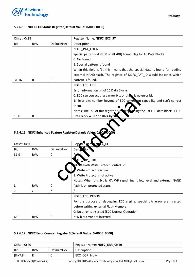
Memory
H3 Datasheet(Revision1.2) Copyright© 2015 Allwinner Technology Co.,Ltd.All Rights Reserved. Page 373
5.2.6.15. NDFC ECC Status Register(Default Value: 0x00000000)
Offset: 0x38 Register Name: NDFC_ECC_ST
Bit R/W Default/Hex Description
31:16 R 0
NDFC_PAT_FOUND
Special pattern (all 0x00 or all x0ff) Found Flag for 16 Data Blocks
0: No Found
1: Special pattern is found
When this field is ‘1’, this means that the special data is found for reading
external NAND flash. The register of NDFC_PAT_ID would indicates which
pattern is found.
15:0 R 0
NDFC_ECC_ERR
Error information bit of 16 Data Blocks
0: ECC can correct these error bits or there is no error bit
1: Error bits number beyond of ECC correction capability and can’t correct
them
Notes: The LSB of this register is corresponding the 1st ECC data block. 1 ECC
Data Block = 512 or 1024 bytes.
5.2.6.16. NDFC Enhanced Feature Register(Default Value: 0x00000000)
Offset: 0x3C Register Name: NDFC_EFR
Bit R/W Default/Hex Description
31:9 R/W 0 /
8 R/W 0
NDFC_WP_CTRL
NAND Flash Write Protect Control Bit
0: Write Protect is active
1: Write Protect is not active
Notes: When this bit is ‘0’, WP signal line is low level and external NAND
flash is on protected state.
7 / / /
6:0 R/W 0
NDFC_ECC_DEBUG
For the purpose of debugging ECC engine, special bits error are inserted
before writing external Flash Memory.
0: No error is inserted (ECC Normal Operation)
n: N bits error are inserted
5.2.6.17. NDFC Error Counter Register 0(Default Value: 0x0000_0000)
Offset: 0x40 Register Name: NDFC_ERR_CNT0
Bit R/W Default/Hex Description
[8i+7:8i] R 0 ECC_COR_NUM
confid
ential
Memory
H3 Datasheet(Revision1.2) Copyright© 2015 Allwinner Technology Co.,Ltd.All Rights Reserved. Page 374
(i=0~3) ECC Corrected Bits Number for ECC Data Block[n] (n from 0 to 3)
0: No corrected bits
1: 1 corrected bit
2: 2 corrected bits
…
64: 64 corrected bits
Others: Reserved
Notes: 1 ECC Data Block = 512 or 1024 bytes
5.2.6.18. NDFC Error Counter Register 1(Default Value: 0x00000000)
Offset: 0x44 Register Name: NDFC_ERR_CNT1
Bit R/W Default/Hex Description
[8i+7:8i]
(i=0~3) R 0
ECC_COR_NUM
ECC Corrected Bits Number for ECC Data Block[n] (n from 4 to 7)
0: No corrected bits
1: 1 corrected bit
2: 2 corrected bits
…
64: 64 corrected bits
Others: Reserved
Notes: 1 ECC Data Block = 512 or 1024 bytes
5.2.6.19. NDFC Error Counter Register 2(Default Value: 0x00000000)
Offset: 0x48 Register Name: NDFC_ERR_CNT2
Bit R/W Default/Hex Description
[8i+7:8i]
(i=0~3) R 0
ECC_COR_NUM
ECC Corrected Bits Number for ECC Data Block[n] (n from 8 to 11)
0: No corrected bits
1: 1 corrected bit
2: 2 corrected bits
…
64: 64 corrected bits
Others: Reserved
Notes: 1 ECC Data Block = 512 or 1024 bytes
5.2.6.20. NDFC Error Counter Register 3(Default Value: 0x00000000)
Offset: 0x4C Register Name: NDFC_ERR_CNT3
Bit R/W Default/Hex Description
confid
ential
Memory
H3 Datasheet(Revision1.2) Copyright© 2015 Allwinner Technology Co.,Ltd.All Rights Reserved. Page 375
[8i+7:8i]
(i=0~3) R 0
ECC_COR_NUM
ECC Corrected Bits Number for ECC Data Block[n] (n from 12 to 15)
0: No corrected bits
1: 1 corrected bit
2: 2 corrected bits
…
64: 64 corrected bits
Others: Reserved
Notes: 1 ECC Data Block = 512 or 1024 bytes
5.2.6.21. NDFC User Data Register [n]( Default Value: 0xffffffff)
Offset: 0x50 + 0x4*n Register Name: NDFC_USER_DATAn
Bit R/W Default/Hex Description
31:0 R/W 0xffffffff
USER_DATA
User Data for ECC Data Block[n] (n from 0 to 15)
Notes: 1 ECC Data Block = 512 or 1024 bytes
Notes: n from 0 to 15
5.2.6.22. NDFC EFNAND STATUS Register(Default Value: 0x00000000)
Offset: 0x90 Register Name: NDFC_EFNAND_STATUS
Bit R/W Default/Hex Description
31:8 / / /
7:0 R 0x0
EF_NAND_STATUS
The Status Value for EF-NAND Page Read operation
5.2.6.23. NDFC Spare Area Register(Default Value: 0x00000400)
Offset: 0xA0 Register Name: NDFC_SPARE_AREA
Bit R/W Default/Hex Description
31:16 / / /
15:0 R/W 0x400
NDFC_SPARE_ADR
This value indicates the spare area first byte address for NDFC interleave
page operation.
5.2.6.24. NDFC Pattern ID Register(Default Value: 0x00000000)
Offset: 0xA4 Register Name: NDFC_PAT_ID
confid
ential

Memory
H3 Datasheet(Revision1.2) Copyright© 2015 Allwinner Technology Co.,Ltd.All Rights Reserved. Page 376
Bit R/W Default/Hex Description
[2i+1:2i]
(i=0~15) R 0
PAT_ID
Special Pattern ID for 16 ECC data block
0: All 0x00 is found
1: All 0xFF is found
Others: Reserved
5.2.6.25. NDFC Read Data Status Control Register(Default Value: 0x01000000)
Offset: 0xA8 Register Name: NDFC_RDATA_STA_CTL
Bit R/W Default/Hex Description
31:25 / / /
24 R/W 1
NDFC_RDATA_STA_EN
0: Disable to count the number of bit 1 and bit 0 during current read
operation;
1: Enable to count the number of bit 1 and bit 0 during current read
operation;
The number of bit 1 and bit 0 during current read operation can be used to
check whether a page is blank or bad.
23:18 / / /
17:0 R/W 0
NDFC_RDATA_STA_TH
The threshold value to generate data status.
If the number of bit 1 during current read operation is less than or equal to
threshold value, the bit 13 of NDFC_ST register will be set.
If the number of bit 0 during current read operation is less than or equal to
threshold value, the bit 12 of NDFC_ST register will be set.
5.2.6.26. NDFC Read Data Status Register 0(Default Value: 0x00000000)
Offset: 0xAC Register Name: NDFC_RDATA_STA_0
Bit R/W Default/Hex Description
31:0 R 0
BIT_CNT_1
The number of input bit 1 during current command. It will be cleared
automatically when next command is executed.
5.2.6.27. NDFC Read Data Status Register 1(Default Value: 0x00000000)
Offset: 0xB0 Register Name: NDFC_RDATA_STA_1
Bit R/W Default/Hex Description
31:0 R 0
BIT_CNT_0
The number of input bit 0 during current command. It will be cleared
confid
ential
Memory
H3 Datasheet(Revision1.2) Copyright© 2015 Allwinner Technology Co.,Ltd.All Rights Reserved. Page 377
automatically when next command is executed.
5.2.6.28. NDFC MBUS DMA Address Register(Default Value: 0x00000000)
Offset: 0xC0 Register Name: NDFC_MDMA_ADDR
Bit R/W Default/Hex Description
31:0 R/W 0
MDMA_ADDR
MBUS DMA address
5.2.6.29. NDFC MBUS DMA Byte Counter Register(Default Value: 0x00000000)
Offset: 0xC4 Register Name: NDFC_MDMA_CNT
Bit R/W Default/Hex Description
14:0 R/W 0
MDMA_CNT
MBUS DMA data counter
confid
ential
Memory
H3 Datasheet(Revision1.2) Copyright© 2015 Allwinner Technology Co.,Ltd.All Rights Reserved. Page 378
5.3. SD/MMC
5.3.1. Overview
The SD/MMC controller can be configured either as a Secure Digital Multimedia Card controller, which simultaneously
supports Secure Digital memory (SD Memory), Secure Digital I/O (SDIO), Multimedia Cards (MMC), eMMC Card.
The SD/MMC controller includes the following features:
Supports Secure Digital memory protocol commands (up to SD2.0)
Supports Secure Digital I/O protocol commands
Supports Multimedia Card protocol commands (up to eMMC4.41)
Supports eMMC boot operation
Supports one SD (Verson1.0 to 2.0) or MMC (Verson3.3 to eMMC4.41)
Supports hardware CRC generation and error detection
Supports host pull-up control
Supports SDIO interrupts in 1-bit and 4-bit modes
Supports SDIO suspend and resume operation
Supports SDIO read wait
Supports block size of 1 to 65535 bytes
Supports descriptor-based internal DMA controller
Internal 128 bytes FIFO for data transfer
confid
ential

Memory
H3 Datasheet(Revision1.2) Copyright© 2015 Allwinner Technology Co.,Ltd.All Rights Reserved. Page 379
5.3.2. Block Diagram
Figure 5-16. SD/MMC Controller Block Diagram
5.3.3. SD/MMC Controller Timing Diagram
Please refer to relative specifications:
Physical Layer Specification Ver2.00 Final
SDIO Specification Ver2.00
Multimedia Cards (MMC – version 4.2)
JEDEC Standard – JESD84-44, EMBEDDED MULTI-MEDIA CARD (e•MMC)
5.3.4. SD/MMC Controller Special Requirement
5.3.4.1. SD/MMC Pin List
Port Name Width Direction Description
SD_CCLK 1 OUT Clock output for SD/SDIO/MMC card
SD_CCMD 1 IN/OUT CMD line
SD_CDATA 4/8 IN/OUT Data line
confid
ential
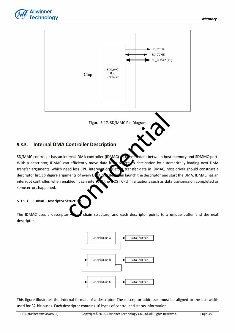
Memory
H3 Datasheet(Revision1.2) Copyright© 2015 Allwinner Technology Co.,Ltd.All Rights Reserved. Page 380
Figure 5-17. SD/MMC Pin Diagram
5.3.5. Internal DMA Controller Description
SD/MMC controller has an internal DMA controller (IDMAC) to transfer data between host memory and SDMMC port.
With a descriptor, IDMAC can efficiently move data from source to destination by automatically loading next DMA
transfer arguments, which need less CPU intervention. Before transfer data in IDMAC, host driver should construct a
descriptor list, configure arguments of every DMA transfer, then launch the descriptor and start the DMA. IDMAC has an
interrupt controller, when enabled, it can interrupt the HOST CPU in situations such as data transmission completed or
some errors happened.
5.3.5.1. IDMAC Descriptor Structure
The IDMAC uses a descriptor with a chain structure, and each descriptor points to a unique buffer and the next
descriptor.
This figure illustrates the internal formats of a descriptor. The descriptor addresses must be aligned to the bus width
used for 32-bit buses. Each descriptor contains 16 bytes of control and status information.
confid
ential
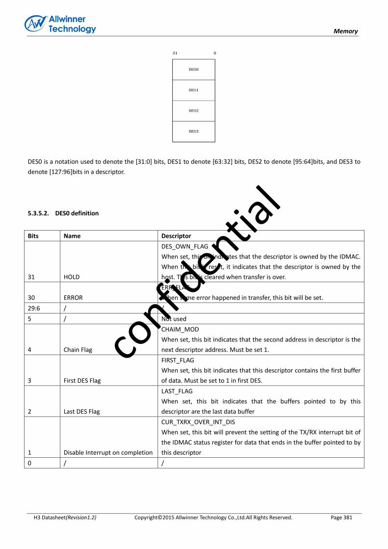
Memory
H3 Datasheet(Revision1.2) Copyright© 2015 Allwinner Technology Co.,Ltd.All Rights Reserved. Page 381
DES0 is a notation used to denote the [31:0] bits, DES1 to denote [63:32] bits, DES2 to denote [95:64]bits, and DES3 to
denote [127:96]bits in a descriptor.
5.3.5.2. DES0 definition
Bits Name Descriptor
31 HOLD
DES_OWN_FLAG
When set, this bit indicates that the descriptor is owned by the IDMAC.
When this bit is reset, it indicates that the descriptor is owned by the
host. This bit is cleared when transfer is over.
30 ERROR
ERR_FLAG
When some error happened in transfer, this bit will be set.
29:6 / /
5 / Not used
4 Chain Flag
CHAIM_MOD
When set, this bit indicates that the second address in descriptor is the
next descriptor address. Must be set 1.
3 First DES Flag
FIRST_FLAG
When set, this bit indicates that this descriptor contains the first buffer
of data. Must be set to 1 in first DES.
2 Last DES Flag
LAST_FLAG
When set, this bit indicates that the buffers pointed to by this
descriptor are the last data buffer
1 Disable Interrupt on completion
CUR_TXRX_OVER_INT_DIS
When set, this bit will prevent the setting of the TX/RX interrupt bit of
the IDMAC status register for data that ends in the buffer pointed to by
this descriptor
0 / /
confid
ential
Memory
H3 Datasheet(Revision1.2) Copyright© 2015 Allwinner Technology Co.,Ltd.All Rights Reserved. Page 382
5.3.5.3. DES1 definition
Bits Name Descriptor
31:16 / /
15:0 Buffer size
BUFF_SIZE
These bits indicate the data buffer byte size, which must be a multiple
of 4 bytes. If this filed is 0, the DMA ignores this buffer and proceeds to
the next descriptor.
5.3.5.4. DES2 definition
Bits Name Descriptor
31:0 Buffer address pointer
BUFF_ADDR
These bits indicate the physical address of data buffer. The IDMAC
ignores DES2[1:0], corresponding to the bus width of 32.
5.3.5.5. DES3 definition
Bits Name Descriptor
31:0 Next descriptor address
NEXT_DESP_ADDR
These bits indicate the pointer to the physical memory where the next
descriptor is present.
5.3.6. SD/MMC Register List
Module Name Base Address
SD/MMC0 0x01C0F000
SD/MMC1 0x01C10000
SD/MMC2 0x01C11000
Register Name Offset Description
SD_GCTL 0x00 Control register
SD_CKCR 0x04 Clock Control register
SD_TMOR 0x08 Time out register
SD_BWDR 0x0C Bus Width register
SD_BKSR 0x10 Block size register
SD_BYCR 0x14 Byte count register
SD_CMDR 0x18 Command register
SD_CAGR 0x1C Command argument register
SD_RESP0 0x20 Response 0 register
confid
ential
Memory
H3 Datasheet(Revision1.2) Copyright© 2015 Allwinner Technology Co.,Ltd.All Rights Reserved. Page 383
SD_RESP1 0x24 Response 1 register
SD_RESP2 0x28 Response 2 register
SD_RESP3 0x2C Response 3 register
SD_IMKR 0x30 Interrupt mask register
SD_MISR 0x34 Masked interrupt status register
SD_RISR 0x38 Raw interrupt status register
SD_STAR 0x3C Status register
SD_FWLR 0x40 FIFO Water Level register
SD_FUNS 0x44 FIFO Function Select register
SD_A12A 0x58 Auto command 12 argument
SD_NTSR 0x5C SD NewTiming Set Register
SD_SDBG 0x60 SD NewTiming Set Debug Register
SD_HWRST 0x78 Hardware Reset Register
SD_DMAC 0x80 BUS Mode Control
SD_DLBA 0x84 Descriptor List Base Address
SD_IDST 0x88 DMAC Status
SD_IDIE 0x8C DMAC Interrupt Enable
SD_THLDC 0x100 Card Threshold Control register
SD_DSBD 0x10C eMMC4.41 DDR Start Bit Detection Control
SD_RES_CRC 0x110 CRC status from card/eMMC in write operation
SD_DATA7_CRC 0x114 CRC Data7 from card/eMMC
SD_DATA6_CRC 0x118 CRC Data7 from card/eMMC
SD_DATA5_CRC 0x11C CRC Data7 from card/eMMC
SD_DATA4_CRC 0x120 CRC Data7 from card/eMMC
SD_DATA3_CRC 0x124 CRC Data7 from card/eMMC
SD_DATA2_CRC 0x128 CRC Data7 from card/eMMC
SD_DATA1_CRC 0x12C CRC Data7 from card/eMMC
SD_DATA0_CRC 0x130 CRC Data7 from card/eMMC
SD_CRC_STA 0x134 Response CRC from card/eMMC
SD_FIFO 0X200 Read/Write FIFO
5.3.7. SD/MMC Register Description
5.3.7.1. SD Global Control Register(Default Value: 0x00000300)
Offset: 0x0000 Register Name: SD_CTRL
Bit R/W Default/Hex Description
31 R/W 0
FIFO_AC_MOD
FIFO Access Mode
1-AHB bus
0-DMA bus
30:11 - - /
confid
ential

Memory
H3 Datasheet(Revision1.2) Copyright© 2015 Allwinner Technology Co.,Ltd.All Rights Reserved. Page 384
10 R/W 0
DDR_MOD_SEL
DDR Mode Select
0 – SDR mode
1 – DDR mode
9 - - reserved
8 R/W 1
CD_DBC_ENB
Card Detect (Data[3] status) De-bounce Enable
0 - disable de-bounce
1 – enable de-bounce
7:6 - - /
5 R/W 0
DMA_ENB
DMA Global Enable
0 – Disable DMA to transfer data, using AHB bus
1 – Enable DMA to transfer data
4 R/W 0
INT_ENB
Global Interrupt Enable
0 – Disable interrupts
1 – Enable interrupts
3 - - /
2 R/W 0 DMA_RST
DMA Reset
1 R/W 0
FIFO_RST
FIFO Reset
0 – No change
1 – Reset FIFO
This bit is auto-cleared after completion of reset operation.
0 R/W 0
SOFT_RST
Software Reset
0 – No change
1 – Reset SD/MMC controller
This bit is auto-cleared after completion of reset operation.
5.3.7.2. SD Clock Control Register(Default Value: 0x00000000)
Offset: 0x0004 Register Name: SD_CLKDIV
Bit R/W Default/Hex Description
31 R/W 0
MASK_DATA0
0 - Do not mask data0 when updata clock ;
1 - Mask data0 when updata clock;
30:18 / / /
17 R/W 0
CCLK_CTRL
Card Clock Output Control
0 – Card clock always on
1 – Turn off card clock when FSM in IDLE state
confid
ential
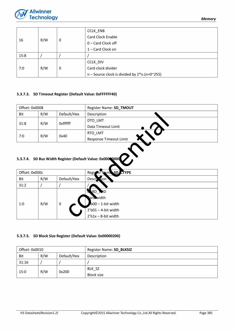
Memory
H3 Datasheet(Revision1.2) Copyright© 2015 Allwinner Technology Co.,Ltd.All Rights Reserved. Page 385
16 R/W 0
CCLK_ENB
Card Clock Enable
0 – Card Clock off
1 – Card Clock on
15:8 / / /
7:0 R/W 0
CCLK_DIV
Card clock divider
n – Source clock is divided by 2*n.(n=0~255)
5.3.7.3. SD Timeout Register (Default Value: 0xFFFFFF40)
Offset: 0x0008 Register Name: SD_TMOUT
Bit R/W Default/Hex Description
31:8 R/W 0xffffff DTO_LMT
Data Timeout Limit
7:0 R/W 0x40 RTO_LMT
Response Timeout Limit
5.3.7.4. SD Bus Width Register (Default Value: 0x00000000)
Offset: 0x000c Register Name: SD_CTYPE
Bit R/W Default/Hex Description
31:2 / / /
1:0 R/W 0
CARD_WID
Card width
2’b00 – 1-bit width
2’b01 – 4-bit width
2’b1x – 8-bit width
5.3.7.5. SD Block Size Register (Default Value: 0x00000200)
Offset: 0x0010 Register Name: SD_BLKSIZ
Bit R/W Default/Hex Description
31:16 / / /
15:0 R/W 0x200 BLK_SZ
Block size
confid
ential
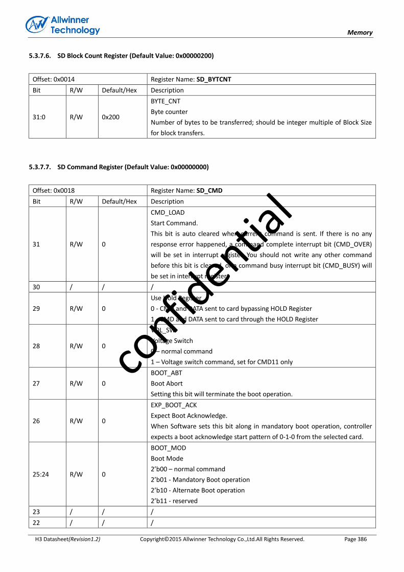
Memory
H3 Datasheet(Revision1.2) Copyright© 2015 Allwinner Technology Co.,Ltd.All Rights Reserved. Page 386
5.3.7.6. SD Block Count Register (Default Value: 0x00000200)
Offset: 0x0014 Register Name: SD_BYTCNT
Bit R/W Default/Hex Description
31:0 R/W 0x200
BYTE_CNT
Byte counter
Number of bytes to be transferred; should be integer multiple of Block Size
for block transfers.
5.3.7.7. SD Command Register (Default Value: 0x00000000)
Offset: 0x0018 Register Name: SD_CMD
Bit R/W Default/Hex Description
31 R/W 0
CMD_LOAD
Start Command.
This bit is auto cleared when current command is sent. If there is no any
response error happened, a command complete interrupt bit (CMD_OVER)
will be set in interrupt register. You should not write any other command
before this bit is cleared, or a command busy interrupt bit (CMD_BUSY) will
be set in interrupt register.
30 / / /
29 R/W 0
Use Hold Register
0 - CMD and DATA sent to card bypassing HOLD Register
1 - CMD and DATA sent to card through the HOLD Register
28 R/W 0
VOL_SW
Voltage Switch
0 – normal command
1 – Voltage switch command, set for CMD11 only
27 R/W 0
BOOT_ABT
Boot Abort
Setting this bit will terminate the boot operation.
26 R/W 0
EXP_BOOT_ACK
Expect Boot Acknowledge.
When Software sets this bit along in mandatory boot operation, controller
expects a boot acknowledge start pattern of 0-1-0 from the selected card.
25:24 R/W 0
BOOT_MOD
Boot Mode
2’b00 – normal command
2’b01 - Mandatory Boot operation
2’b10 - Alternate Boot operation
2’b11 - reserved
23 / / /
22 / / /
confid
ential
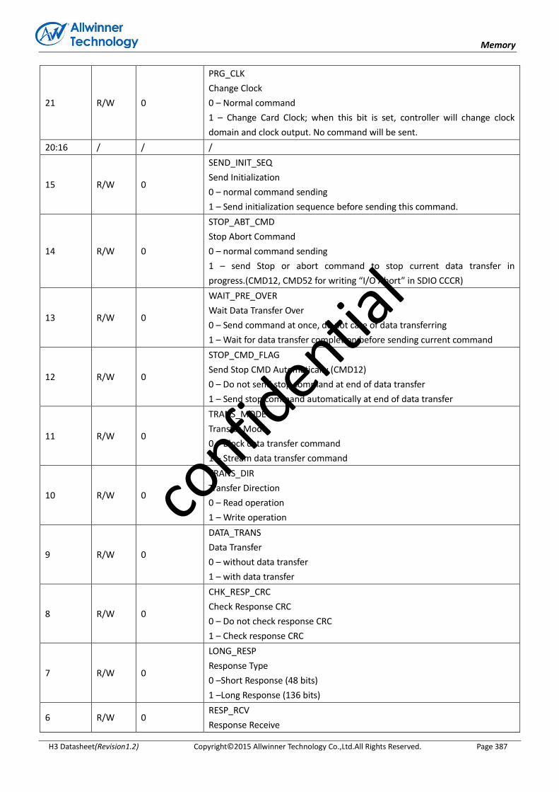
Memory
H3 Datasheet(Revision1.2) Copyright© 2015 Allwinner Technology Co.,Ltd.All Rights Reserved. Page 387
21 R/W 0
PRG_CLK
Change Clock
0 – Normal command
1 – Change Card Clock; when this bit is set, controller will change clock
domain and clock output. No command will be sent.
20:16 / / /
15 R/W 0
SEND_INIT_SEQ
Send Initialization
0 – normal command sending
1 – Send initialization sequence before sending this command.
14 R/W 0
STOP_ABT_CMD
Stop Abort Command
0 – normal command sending
1 – send Stop or abort command to stop current data transfer in
progress.(CMD12, CMD52 for writing “I/O Abort” in SDIO CCCR)
13 R/W 0
WAIT_PRE_OVER
Wait Data Transfer Over
0 – Send command at once, do not care of data transferring
1 – Wait for data transfer completion before sending current command
12 R/W 0
STOP_CMD_FLAG
Send Stop CMD Automatically (CMD12)
0 – Do not send stop command at end of data transfer
1 – Send stop command automatically at end of data transfer
11 R/W 0
TRANS_MODE
Transfer Mode
0 – Block data transfer command
1 – Stream data transfer command
10 R/W 0
TRANS_DIR
Transfer Direction
0 – Read operation
1 – Write operation
9 R/W 0
DATA_TRANS
Data Transfer
0 – without data transfer
1 – with data transfer
8 R/W 0
CHK_RESP_CRC
Check Response CRC
0 – Do not check response CRC
1 – Check response CRC
7 R/W 0
LONG_RESP
Response Type
0 –Short Response (48 bits)
1 –Long Response (136 bits)
6 R/W 0 RESP_RCV
Response Receive
confid
ential

Memory
H3 Datasheet(Revision1.2) Copyright© 2015 Allwinner Technology Co.,Ltd.All Rights Reserved. Page 388
0 – Command without Response
1 – Command with Response
5:0 R/W 0
CMD_IDX
CMD Index
Command index value
5.3.7.8. SD Command Argument Register (Default Value: 0x00000000)
Offset: 0x001c Register Name: SD_CMDARG
Bit R/W Default/Hex Description
31:0 R/W 0 CMD_ARG
Command argument
5.3.7.9. SD Response 0 Register (Default Value: 0x00000000)
Offset: 0x0020 Register Name: SD_RESP0
Bit R/W Default/Hex Description
31:0 R 0 CMD_RESP0
response 0
Bit[31:0] of response
5.3.7.10. SD Response 1 Register (Default Value: 0x00000000)
Offset: 0x0024 Register Name: SD_RESP1
Bit R/W Default/Hex Description
31:0 R 0 CMD_RESP1
response 1
Bit[63:31] of response
5.3.7.11. SD Response 2 Register (Default Value: 0x00000000)
Offset: 0x0028 Register Name: SD_RESP2
Bit R/W Default/Hex Description
31:0 R 0 CMD_RESP2
response 2
Bit[95:64] of response
confid
ential

Memory
H3 Datasheet(Revision1.2) Copyright© 2015 Allwinner Technology Co.,Ltd.All Rights Reserved. Page 389
5.3.7.12. SD Response 3 Register (Default Value: 0x00000000)
Offset: 0x002C Register Name: SD_RESP3
Bit R/W Default/Hex Description
31:0 R 0 CMD_RESP3
response 3
Bit[127:96] of response
5.3.7.13. SD Interrupt Mask Register (Default Value: 0x00000000)
Offset: 0x0030 Register Name: SD_INTMASK
Bit R/W Default/Hex Description
31:0 R/W 0
INT_MASK
0 – interrupt masked
1 – interrupt enabled
Bit field defined as following:
bit 31– card removed
bit 30 – card inserted
bit 17~29 - reserved
bit 16 – SDIO interrupt
bit 15 – Data End-bit error
bit 14 – Auto Stop Command done
bit 13 – Data Start Error
bit 12 – Command Busy and illegal write
bit 11 – FIFO under run/overflow
bit 10 – Data starvation timeout /V1.8 Switch Done
bit 9 – Data timeout/Boot data start
bit 8 – Response timeout/Boot ACK received
bit 7 – Data CRC error
bit 6 – Response CRC error
bit 5 – Data Receive Request
bit 4 –Data Transmit Request
bit 3 – Data Transfer Complete
bit 2 – Command Complete
bit 1 – Response Error (no response or response CRC error)
bit 0 – Reserved
5.3.7.14. SD Masked Interrupt Status Register (Default Value: 0x00000000)
Offset: 0x0034 Register Name: SD_MINTSTS
Bit R/W Default/Hex Description
confid
ential
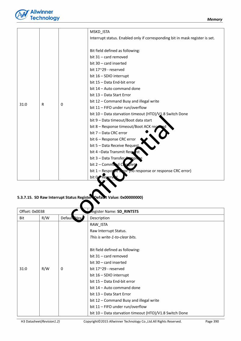
Memory
H3 Datasheet(Revision1.2) Copyright© 2015 Allwinner Technology Co.,Ltd.All Rights Reserved. Page 390
31:0 R 0
MSKD_ISTA
Interrupt status. Enabled only if corresponding bit in mask register is set.
Bit field defined as following:
bit 31 – card removed
bit 30 – card inserted
bit 17~29 - reserved
bit 16 – SDIO interrupt
bit 15 – Data End-bit error
bit 14 – Auto command done
bit 13 – Data Start Error
bit 12 – Command Busy and illegal write
bit 11 – FIFO under run/overflow
bit 10 – Data starvation timeout (HTO)/V1.8 Switch Done
bit 9 – Data timeout/Boot data start
bit 8 – Response timeout/Boot ACK received
bit 7 – Data CRC error
bit 6 – Response CRC error
bit 5 – Data Receive Request
bit 4 –Data Transmit Request
bit 3 – Data Transfer Complete
bit 2 – Command Complete
bit 1 – Response Error (no response or response CRC error)
bit 0 – Reserved
5.3.7.15. SD Raw Interrupt Status Register (Default Value: 0x00000000)
Offset: 0x0038 Register Name: SD_RINTSTS
Bit R/W Default/Hex Description
31:0 R/W 0
RAW_ISTA
Raw Interrupt Status.
This is write-1-to-clear bits.
Bit field defined as following:
bit 31 – card removed
bit 30 – card inserted
bit 17~29 - reserved
bit 16 – SDIO interrupt
bit 15 – Data End-bit error
bit 14 – Auto command done
bit 13 – Data Start Error
bit 12 – Command Busy and illegal write
bit 11 – FIFO under run/overflow
bit 10 – Data starvation timeout (HTO)/V1.8 Switch Done
confid
ential

Memory
H3 Datasheet(Revision1.2) Copyright© 2015 Allwinner Technology Co.,Ltd.All Rights Reserved. Page 391
bit 9 – Data timeout/Boot data start
bit 8 – Response timeout/Boot ACK received
bit 7 – Data CRC error
bit 6 – Response CRC error
bit 5 – Data Receive Request
bit 4 –Data Transmit Request
bit 3 – Data Transfer Complete
bit 2 – Command Complete
bit 1 – Response Error (no response or response CRC error)
bit 0 – Reserved
5.3.7.16. SD Status Register (Default Value: 0x00000006)
Offset: 0x003C Register Name: SD_STATUS
Bit R/W Default/Hex Description
31 R 0
DMA_REQ
dma_req
DMA request signal state
30:22 / / /
21:17 R 0
FIFO_LEVEL
FIFO Level
Number of filled locations in FIFO
16:11 R 0
RESP_IDX
Response Index
Index of previous response, including any auto-stop sent by controller
10 R 0
FSM_BUSY
Data FSM Busy
Data transmit or receive state-machine is busy
9 R 0
CARD_BUSY
Card data busy
Inverted version of DATA[0]
0 – card data not busy
1 – card data busy
8 R 0
CARD_PRESENT
Data[3] status
level of DATA[3]; checks whether card is present
0 – card not present
1 – card present
7:4 R 0
FSM_STA
Command FSM states:
0 – Idle
1 – Send init sequence
2 – Tx cmd start bit
3 – Tx cmd tx bit
confid
ential

Memory
H3 Datasheet(Revision1.2) Copyright© 2015 Allwinner Technology Co.,Ltd.All Rights Reserved. Page 392
4 – Tx cmd index + arg
5 – Tx cmd crc7
6 – Tx cmd end bit
7 – Rx resp start bit
8 – Rx resp IRQ response
9 – Rx resp tx bit
10 – Rx resp cmd idx
11 – Rx resp data
12 – Rx resp crc7
13 – Rx resp end bit
14 – Cmd path wait NCC
15 – Wait; CMD-to-response turnaround
3 R 0
FIFO_FULL
FIFO full
1 – FIFO full
0 – FIFO not full
2 R 1
FIFO_EMPTY
FIFO Empty
1 - FIFO Empty
0 - FIFO not Empty
1 R 1
FIFO_TX_LEVEL
FIFO TX Water Level flag
0 – FIFO didn’t reach transmit trigger level
1 - FIFO reached transmit trigger level
0 R 0
FIFO_RX_LEVEL
FIFO TX Water Level flag
0 – FIFO didn’t reach receive trigger level
1 - FIFO reached receive trigger level
5.3.7.17. SD FIFO Water Level Register (Default Value: 0x000F0000)
Offset: 0x0040 Register Name: SD_FIFOTH
Bit R/W Default/Hex Description
31 / / /
30:28 R/W 0
BSIZE_OF_TRANS
Burst size of multiple transaction
000 – 1 transfers
001 – 4
010 – 8
011 – 16
100 – 32
101 – 64
110 – 128
111 – 256
confid
ential
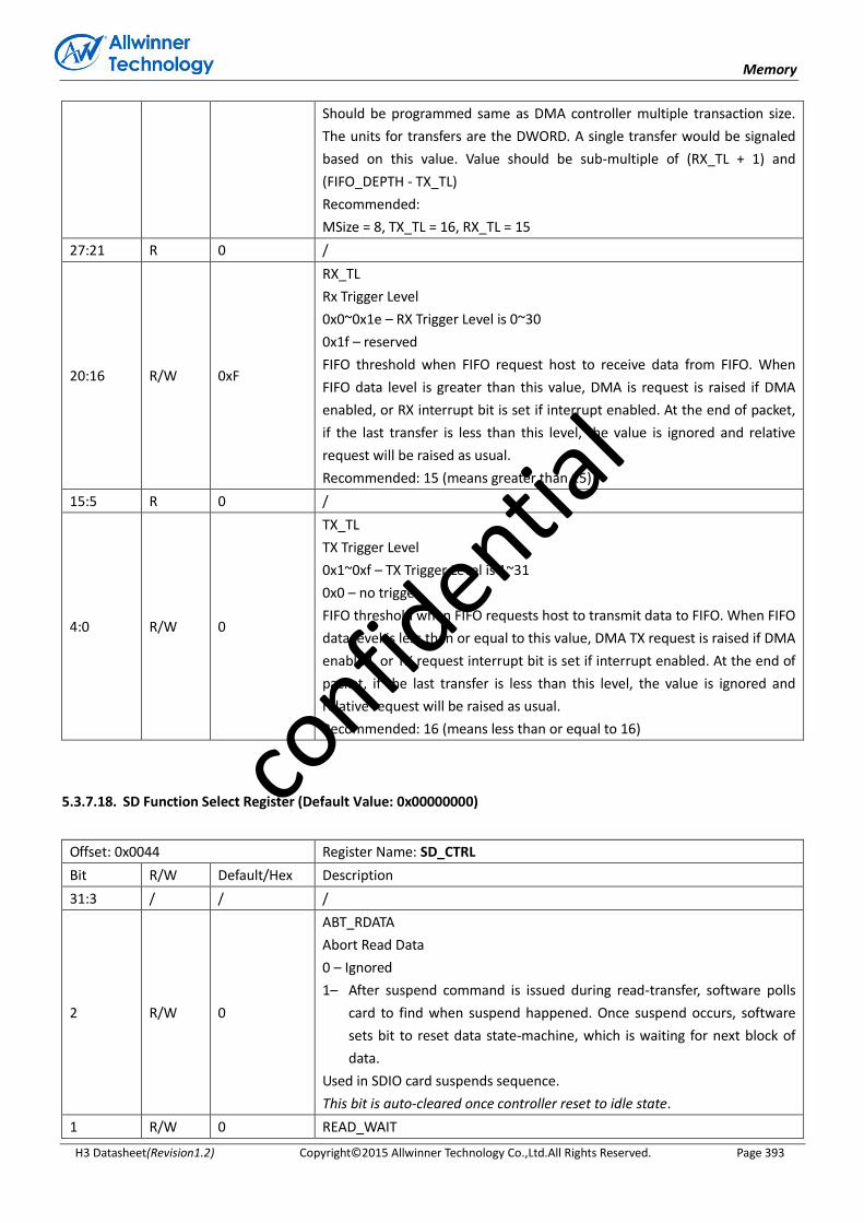
Memory
H3 Datasheet(Revision1.2) Copyright© 2015 Allwinner Technology Co.,Ltd.All Rights Reserved. Page 393
Should be programmed same as DMA controller multiple transaction size.
The units for transfers are the DWORD. A single transfer would be signaled
based on this value. Value should be sub-multiple of (RX_TL + 1) and
(FIFO_DEPTH - TX_TL)
Recommended:
MSize = 8, TX_TL = 16, RX_TL = 15
27:21 R 0 /
20:16 R/W 0xF
RX_TL
Rx Trigger Level
0x0~0x1e – RX Trigger Level is 0~30
0x1f – reserved
FIFO threshold when FIFO request host to receive data from FIFO. When
FIFO data level is greater than this value, DMA is request is raised if DMA
enabled, or RX interrupt bit is set if interrupt enabled. At the end of packet,
if the last transfer is less than this level, the value is ignored and relative
request will be raised as usual.
Recommended: 15 (means greater than 15)
15:5 R 0 /
4:0 R/W 0
TX_TL
TX Trigger Level
0x1~0xf – TX Trigger Level is 1~31
0x0 – no trigger
FIFO threshold when FIFO requests host to transmit data to FIFO. When FIFO
data level is less than or equal to this value, DMA TX request is raised if DMA
enabled, or TX request interrupt bit is set if interrupt enabled. At the end of
packet, if the last transfer is less than this level, the value is ignored and
relative request will be raised as usual.
Recommended: 16 (means less than or equal to 16)
5.3.7.18. SD Function Select Register (Default Value: 0x00000000)
Offset: 0x0044 Register Name: SD_CTRL
Bit R/W Default/Hex Description
31:3 / / /
2 R/W 0
ABT_RDATA
Abort Read Data
0 – Ignored
1– After suspend command is issued during read-transfer, software polls
card to find when suspend happened. Once suspend occurs, software
sets bit to reset data state-machine, which is waiting for next block of
data.
Used in SDIO card suspends sequence.
This bit is auto-cleared once controller reset to idle state.
1 R/W 0 READ_WAIT
confid
ential
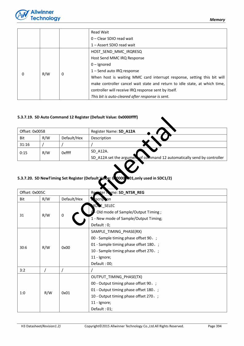
Memory
H3 Datasheet(Revision1.2) Copyright© 2015 Allwinner Technology Co.,Ltd.All Rights Reserved. Page 394
Read Wait
0 – Clear SDIO read wait
1 – Assert SDIO read wait
0 R/W 0
HOST_SEND_MMC_IRQRESQ
Host Send MMC IRQ Response
0 – Ignored
1 – Send auto IRQ response
When host is waiting MMC card interrupt response, setting this bit will
make controller cancel wait state and return to idle state, at which time,
controller will receive IRQ response sent by itself.
This bit is auto-cleared after response is sent.
5.3.7.19. SD Auto Command 12 Register (Default Value: 0x0000ffff)
Offset: 0x0058 Register Name: SD_A12A
Bit R/W Default/Hex Description
31:16 / / /
0:15 R/W 0xffff SD_A12A.
SD_A12A set the argument of command 12 automatically send by controller
5.3.7.20. SD NewTiming Set Register (Default Value: 0x00000001,only used in SDC1/2)
Offset: 0x005C Register Name: SD_NTSR_REG
Bit R/W Default/Hex Description
31 R/W 0
MODE_SELEC
0 - Old mode of Sample/Output Timing ;
1 - New mode of Sample/Output Timing;
Default : 0;
30:6 R/W 0x00
SAMPLE_TIMING_PHASE(RX)
00 - Sample timing phase offset 90。;
01 - Sample timing phase offset 180。;
10 - Sample timing phase offset 270。;
11 - Ignore;
Default : 00;
3:2 / / /
1:0 R/W 0x01
OUTPUT_TIMING_PHASE(TX)
00 - Output timing phase offset 90。;
01 - Output timing phase offset 180。;
10 - Output timing phase offset 270。;
11 - Ignore;
Default : 01;
confid
ential

Memory
H3 Datasheet(Revision1.2) Copyright© 2015 Allwinner Technology Co.,Ltd.All Rights Reserved. Page 395
5.3.7.21. SD Hardware Reset Register (Default Value: 0x00000001)
Offset: 0x0078 Register Name: SD_HWRST
Bit R/W Default/Hex Description
31:1 / / /
0 R/W 1
HW_RESET.
1 – Active mode
0 – Reset
These bits cause the cards to enter pre-idle state, which requires them to be
re-initialized.
5.3.7.22. SD DMAC Control Register (Default Value: 0x00000000)
Offset: 0x0080 Register Name: SD_BUS_MODE
Bit R/W Default/Hex Description
31 W 0
DES_LOAD_CTRL
When DMAC fetches a descriptor, if the valid bit of a descriptor is not set,
DMAC FSM will go to the suspend state. Setting this bit will make DMAC
re-fetch descriptor again and do the transfer normally.
30:11 / / /
10:8 R 0
PRG_BURST_LEN
Programmable Burst Length.
These bits indicate the maximum number of beats to be performed in one
IDMAC transaction. The IDMAC will always attempt to burst as specified in
PBL each time it starts a Burst transfer on the host bus. The permissible
values are 1, 4, 8, 16, 32, 64, 128 and 256. This value is the mirror of MSIZE
of FIFOTH register. In order to change this value, write the required value to
FIFOTH register. This is an encode value as follows.
000 – 1 transfers
001 – 4 transfers
010 – 8 transfers
011 – 16 transfers
100 – 32 transfers
101 – 64 transfers
110 – 128 transfers
111 – 256 transfers
Transfer unit is either 16, 32, or 64 bits, based on HDATA_WIDTH. PBL is a
read-only value.
7 R/W 0
IDMAC_ENB
IDMAC Enable.
When set, the IDMAC is enabled. DE is read/write.
6:2 R/W 0 DES_SKIP_LEN
Descriptor Skip Length.
confid
ential

Memory
H3 Datasheet(Revision1.2) Copyright© 2015 Allwinner Technology Co.,Ltd.All Rights Reserved. Page 396
Specifies the number of Word to skip between two unchained descriptors.
This is applicable only for dual buffer structure.
Default is set to 4 DWORD.
1 R/W 0
FIX_BUST_CTRL
Fixed Burst.
Controls whether the AHB Master interface performs fixed burst transfers or
not. When set, the AHB will use only SINGLE, INCR4, INCR8 during start of
normal burst transfers. When reset, the AHB will use SINGLE and INCR burst
transfer operations.
0 R/W 0
IDMAC_RST
DMA Reset.
When set, the DMA Controller resets all its internal registers. SWR is
read/write. It is automatically cleared after 1 clock cycle.
5.3.7.23. SD Descriptor List Base Address Register (Default Value: 0x00000000)
Offset: 0x0084 Register Name: SD_DLBA
Bit R/W Default/Hex Description
31:0 R/W 0
DES_BASE_ADDR
Start of Descriptor List.
Contains the base address of the First Descriptor. The LSB bits [1:0] are
ignored and taken as all-zero by the IDMAC internally. Hence these LSB bits
are read-only.
5.3.7.24. SD DMAC Status Register (Default Value: 0x0000_0000)
Offset: 0x0088 Register Name: SD_DSR
Bit R/W Default/Hex Description
31:17 / / /
16:13 R 0
DMAC_FSM_STA
DMAC FSM present state.
0 – DMA_IDLE
1 – DMA_SUSPEND
2 – DESC_RD
3 – DESC_CHK
4 – DMA_RD_REQ_WAIT
5 – DMA_WR_REQ_WAIT
6 – DMA_RD
7 – DMA_WR
8 – DESC_CLOSE
This bit is read-only.
12:10 R 0 DMAC_ERR_STA
confid
ential
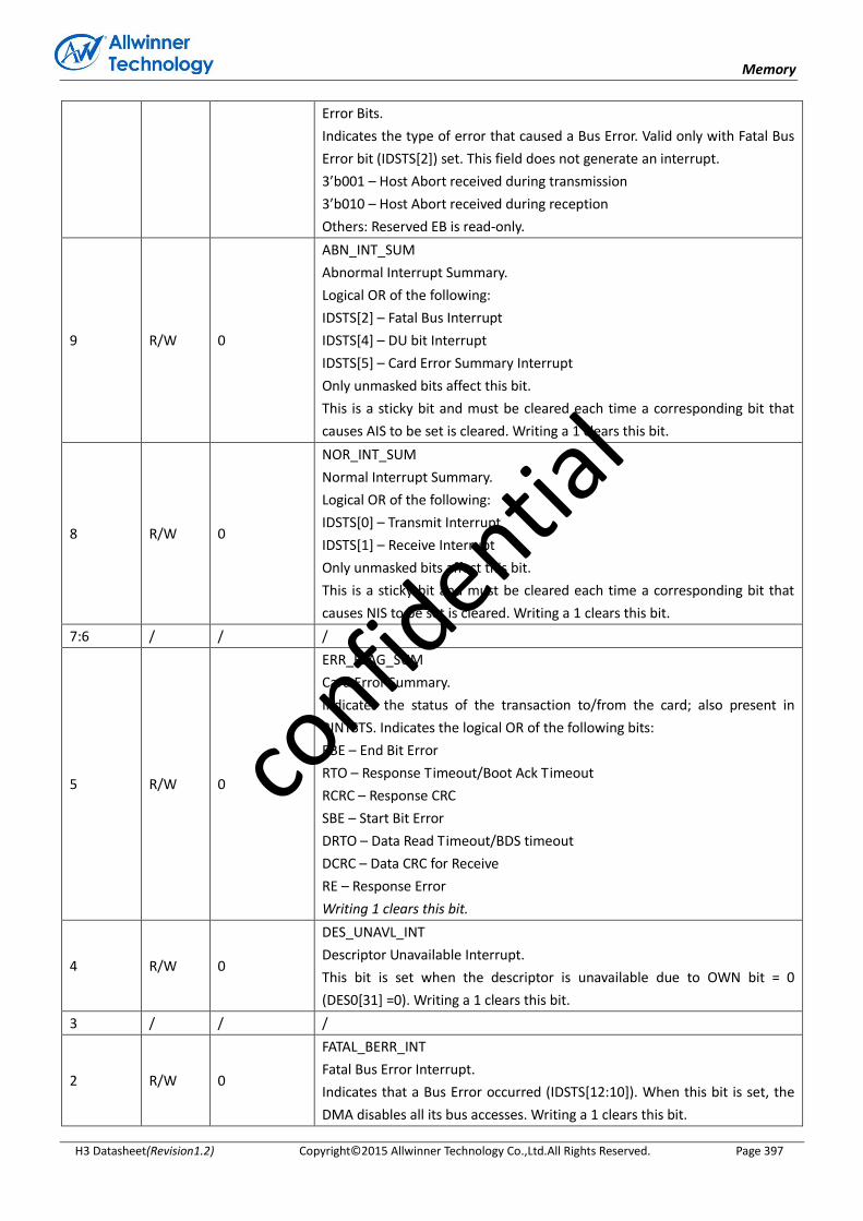
Memory
H3 Datasheet(Revision1.2) Copyright© 2015 Allwinner Technology Co.,Ltd.All Rights Reserved. Page 397
Error Bits.
Indicates the type of error that caused a Bus Error. Valid only with Fatal Bus
Error bit (IDSTS[2]) set. This field does not generate an interrupt.
3’b001 – Host Abort received during transmission
3’b010 – Host Abort received during reception
Others: Reserved EB is read-only.
9 R/W 0
ABN_INT_SUM
Abnormal Interrupt Summary.
Logical OR of the following:
IDSTS[2] – Fatal Bus Interrupt
IDSTS[4] – DU bit Interrupt
IDSTS[5] – Card Error Summary Interrupt
Only unmasked bits affect this bit.
This is a sticky bit and must be cleared each time a corresponding bit that
causes AIS to be set is cleared. Writing a 1 clears this bit.
8 R/W 0
NOR_INT_SUM
Normal Interrupt Summary.
Logical OR of the following:
IDSTS[0] – Transmit Interrupt
IDSTS[1] – Receive Interrupt
Only unmasked bits affect this bit.
This is a sticky bit and must be cleared each time a corresponding bit that
causes NIS to be set is cleared. Writing a 1 clears this bit.
7:6 / / /
5 R/W 0
ERR_FLAG_SUM
Card Error Summary.
Indicates the status of the transaction to/from the card; also present in
RINTSTS. Indicates the logical OR of the following bits:
EBE – End Bit Error
RTO – Response Timeout/Boot Ack Timeout
RCRC – Response CRC
SBE – Start Bit Error
DRTO – Data Read Timeout/BDS timeout
DCRC – Data CRC for Receive
RE – Response Error
Writing 1 clears this bit.
4 R/W 0
DES_UNAVL_INT
Descriptor Unavailable Interrupt.
This bit is set when the descriptor is unavailable due to OWN bit = 0
(DES0[31] =0). Writing a 1 clears this bit.
3 / / /
2 R/W 0
FATAL_BERR_INT
Fatal Bus Error Interrupt.
Indicates that a Bus Error occurred (IDSTS[12:10]). When this bit is set, the
DMA disables all its bus accesses. Writing a 1 clears this bit.
confid
ential
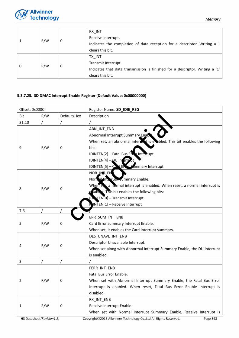
Memory
H3 Datasheet(Revision1.2) Copyright© 2015 Allwinner Technology Co.,Ltd.All Rights Reserved. Page 398
1 R/W 0
RX_INT
Receive Interrupt.
Indicates the completion of data reception for a descriptor. Writing a 1
clears this bit.
0 R/W 0
TX_INT
Transmit Interrupt.
Indicates that data transmission is finished for a descriptor. Writing a ‘1’
clears this bit.
5.3.7.25. SD DMAC Interrupt Enable Register (Default Value: 0x00000000)
Offset: 0x008C Register Name: SD_IDIE_REG
Bit R/W Default/Hex Description
31:10 / / /
9 R/W 0
ABN_INT_ENB
Abnormal Interrupt Summary Enable.
When set, an abnormal interrupt is enabled. This bit enables the following
bits:
IDINTEN[2] – Fatal Bus Error Interrupt
IDINTEN[4] – DU Interrupt
IDINTEN[5] – Card Error Summary Interrupt
8 R/W 0
NOR_INT_ENB
Normal Interrupt Summary Enable.
When set, a normal interrupt is enabled. When reset, a normal interrupt is
disabled. This bit enables the following bits:
IDINTEN[0] – Transmit Interrupt
IDINTEN[1] – Receive Interrupt
7:6 / / /
5 R/W 0
ERR_SUM_INT_ENB
Card Error summary Interrupt Enable.
When set, it enables the Card Interrupt summary.
4 R/W 0
DES_UNAVL_INT_ENB
Descriptor Unavailable Interrupt.
When set along with Abnormal Interrupt Summary Enable, the DU interrupt
is enabled.
3 / / /
2 R/W 0
FERR_INT_ENB
Fatal Bus Error Enable.
When set with Abnormal Interrupt Summary Enable, the Fatal Bus Error
Interrupt is enabled. When reset, Fatal Bus Error Enable Interrupt is
disabled.
1 R/W 0
RX_INT_ENB
Receive Interrupt Enable.
When set with Normal Interrupt Summary Enable, Receive Interrupt is
confid
ential

Memory
H3 Datasheet(Revision1.2) Copyright© 2015 Allwinner Technology Co.,Ltd.All Rights Reserved. Page 399
enabled. When reset, Receive Interrupt is disabled.
0 R/W 0
TX_INT_ENB
Transmit Interrupt Enable.
When set with Normal Interrupt Summary Enable, Transmit Interrupt is
enabled. When reset, Transmit Interrupt is disabled.
5.3.7.26. Card Threshold Control Register (Default Value: 0x00000000)
Offset: 0x0100 Register Name: SD_THLD_REG
Bit R/W Default/Hex Description
31:28 / / /
27:16 R/W 0 CARD_RD_THLD
Card Read Threshold Size
15:1 / / /
0 R/W 0
CARD_RD_THLD_ENB
Card Read Threshold Enable
0 – Card Read Threshold Disable
1 - Card Read Threshold Enable
Host controller initiates Read Transfer only if CARD_RD_THLD amount of
space is available in receive FIFO
5.3.7.27. eMMC4.41 DDR Start Bit Detection Control Register (Default Value: 0x00000000)
Offset: 0x010C Register Name: EMMC_DDR_SBIT_DET_REG
Bit R/W Default/Hex Description
31:1 / / /
0 R/W 0
HALF_START_BIT
Control for start bit detection mechanism inside mstorage based on
duration of start bit.
For eMMC 4.41, start bit can be:
0 - Full cycle
1 - Less than one full cycle
Set HALF_START_BIT=1 for eMMC 4.41 and above; set to 0 for SD
applications.
5.3.7.28. SD Response CRC Register (Default Value: 0x00000000)
Offset: 0x0110 Register Name: RESP_CRC_REG
Bit R/W Default/Hex Description
31:7 / / /
6:0 R 0 RESP_CRC
confid
ential

Memory
H3 Datasheet(Revision1.2) Copyright© 2015 Allwinner Technology Co.,Ltd.All Rights Reserved. Page 400
Response CRC
Response CRC from card/eMMC.
5.3.7.29. SD Data7 CRC Register (Default Value: 0x00000000)
Offset: 0x0114 Register Name: DATA7_CRC_REG
Bit R/W Default/Hex Description
31:0 R 0
DATA7_CRC
Data[7] CRC
CRC in data[7] from card/eMMC.In DDR mode,the higher 16 bits indicate the
CRC of even data,and the lower 16bits indicate the CRC of odd data.In SDR
mode,the higher of 16 bits indicate the CRC of all data.
5.3.7.30. SD Data6 CRC Register (Default Value: 0x00000000)
Offset: 0x0118 Register Name: DATA6_CRC_REG
Bit R/W Default/Hex Description
31:0 R 0
DATA6_CRC
Data[6] CRC
CRC in data[6] from card/eMMC.In DDR mode,the higher 16 bits indicate the
CRC of even data,and the lower 16bits indicate the CRC of odd data.In SDR
mode,the higher of 16 bits indicate the CRC of all data.
5.3.7.31. SD Data5 CRC Register (Default Value: 0x00000000)
Offset: 0x011c Register Name: DATA5_CRC_REG
Bit R/W Default/Hex Description
31:0 R 0
DATA5_CRC
Data[5] CRC
CRC in data[5] from card/eMMC.In DDR mode,the higher 16 bits indicate the
CRC of even data,and the lower 16bits indicate the CRC of odd data.In SDR
mode,the higher of 16 bits indicate the CRC of all data.
5.3.7.32. SD Data4 CRC Register (Default Value: 0x00000000)
Offset: 0x0120 Register Name: DATA4_CRC_REG
Bit R/W Default/Hex Description
31:0 R 0 DATA4_CRC
Data[4] CRC
confid
ential

Memory
H3 Datasheet(Revision1.2) Copyright© 2015 Allwinner Technology Co.,Ltd.All Rights Reserved. Page 401
CRC in data[4] from card/eMMC.In DDR mode,the higher 16 bits indicate the
CRC of even data,and the lower 16bits indicate the CRC of odd data.In SDR
mode,the higher of 16 bits indicate the CRC of all data.
5.3.7.33. SD Data3 CRC Register (Default Value: 0x00000000)
Offset: 0x0124 Register Name: DATA3_CRC_REG
Bit R/W Default/Hex Description
31:0 R 0
DATA3_CRC
Data[3] CRC
CRC in data[3] from card/eMMC.
In 8bit DDR mode,the higher 16 bits indicate the CRC of even data,and the
lower 16bits indicate the CRC of odd data.
In 4 bit DDR mode,the higher of 16 bits indicate the CRC of odd data, ,and
the lower 16bits indicate the CRC of even data.
In SDR mode,the higher of 16 bits indicate the CRC of all data.
5.3.7.34. SD Data2 CRC Register (Default Value: 0x00000000)
Offset: 0x0128 Register Name: DATA2_CRC_REG
Bit R/W Default/Hex Description
31:0 R 0
DATA2_CRC
Data[2] CRC
CRC in data[2] from card/eMMC.
In 8bit DDR mode,the higher 16 bits indicate the CRC of even data,and the
lower 16bits indicate the CRC of odd data.
In 4 bit DDR mode,the higher of 16 bits indicate the CRC of odd data, ,and
the lower 16bits indicate the CRC of even data.
In SDR mode,the higher of 16 bits indicate the CRC of all data.
5.3.7.35. SD Data1 CRC Register (Default Value: 0x00000000)
Offset: 0x012c Register Name: DATA1_CRC_REG
Bit R/W Default/Hex Description
31:0 R 0
DATA1_CRC
Data[1] CRC
CRC in data[1] from card/eMMC.
In 8bit DDR mode,the higher 16 bits indicate the CRC of even data,and the
lower 16bits indicate the CRC of odd data.
In 4 bit DDR mode,the higher of 16 bits indicate the CRC of odd data, ,and
the lower 16bits indicate the CRC of even data.
confid
ential
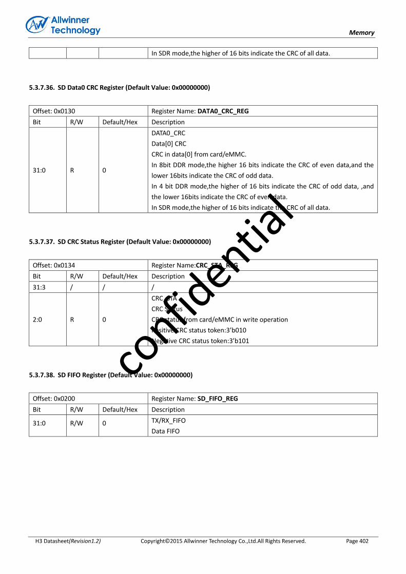
Memory
H3 Datasheet(Revision1.2) Copyright© 2015 Allwinner Technology Co.,Ltd.All Rights Reserved. Page 402
In SDR mode,the higher of 16 bits indicate the CRC of all data.
5.3.7.36. SD Data0 CRC Register (Default Value: 0x00000000)
Offset: 0x0130 Register Name: DATA0_CRC_REG
Bit R/W Default/Hex Description
31:0 R 0
DATA0_CRC
Data[0] CRC
CRC in data[0] from card/eMMC.
In 8bit DDR mode,the higher 16 bits indicate the CRC of even data,and the
lower 16bits indicate the CRC of odd data.
In 4 bit DDR mode,the higher of 16 bits indicate the CRC of odd data, ,and
the lower 16bits indicate the CRC of even data.
In SDR mode,the higher of 16 bits indicate the CRC of all data.
5.3.7.37. SD CRC Status Register (Default Value: 0x00000000)
Offset: 0x0134 Register Name:CRC_STA_REG
Bit R/W Default/Hex Description
31:3 / / /
2:0 R 0
CRC_STA
CRC Status
CRC status from card/eMMC in write operation
Positive CRC status token:3’b010
Negative CRC status token:3’b101
5.3.7.38. SD FIFO Register (Default Value: 0x00000000)
Offset: 0x0200 Register Name: SD_FIFO_REG
Bit R/W Default/Hex Description
31:0 R/W 0 TX/RX_FIFO
Data FIFO
confid
ential

Image
H3 Datasheet(Revision1.2) Copyright© 2015 Allwinner Technology Co.,Ltd.All Rights Reserved. Page 403
Chapter 6 Image
This section describes the image input of H3:
CSI
6.1. CSI
6.1.1. Overview
The CSI includes the following feature:
CSI
Support 8bit yuv422 CMOS sensor interface
Support CCIR656 protocol for NTSC and PAL
Maximum still capture resolution to 5M
Maximum video capture resolution to 1080@30fps
CCI
Compatible with i2c transmission in 7 bit slave ID + 1 bit R/W
Automatic transmission
0/8/16/32 bit register address supported
8/16/32 bit data supported
64bytes-FIFO input CCI data supported
Synchronized with CSI signal and delay trigger supported
Repeated transmission with sync signal supported
confid
ential

Image
H3 Datasheet(Revision1.2) Copyright© 2015 Allwinner Technology Co.,Ltd.All Rights Reserved. Page 404
6.1.2. Functionalities Description
6.1.2.1. Block Diagram
CSI
Formatter
Sy
stem
BU
S
FIFO 2
FIFO 1
FIFO 0
DMA
CS Data
CS Data Clock
CS Hsync
CS Vsync
Channel 0 CS Field
CSI
IF
Converter
DMA
MU
X
Pattern
Generater
YUV Interleaved/Raw IF
CCIR656 IF
Figure 6-1. CSI Block Diagram
SDA CTLCCI FIFO
PAD
CTL
FMT CTL
SCL CTLCLD_DIV24MHz CLK
TRIG
SEL
CSI0/1 1st HREFCSI0/1 last HREF
CSI0/1 Line counter
REGISTER IMMEDIATELY
SDA
SCL
CSI TRIG
DLY CNT
Figure 6-2. CCI Block Diagram
confid
ential
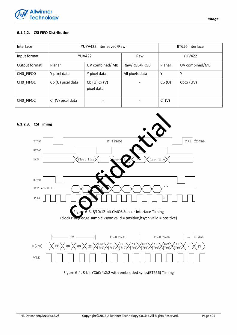
Image
H3 Datasheet(Revision1.2) Copyright© 2015 Allwinner Technology Co.,Ltd.All Rights Reserved. Page 405
6.1.2.2. CSI FIFO Distribution
Interface YUYV422 Interleaved/Raw BT656 Interface
Input format YUV422 Raw YUV422
Output format Planar UV combined/ MB Raw/RGB/PRGB Planar UV combined/MB
CH0_FIFO0 Y pixel data Y pixel data All pixels data Y Y
CH0_FIFO1 Cb (U) pixel data Cb (U) Cr (V)
pixel data
- Cb (U) CbCr (UV)
CH0_FIFO2 Cr (V) pixel data - - Cr (V)
6.1.2.3. CSI Timing
VSYNC
HSYNC
DATA
HSYNC
DATA[7/9/11:0]
PCLK
n frame n+1 frame
…
first line second line last line
…
…
…
Figure 6-3. 8/10/12-bit CMOS Sensor Interface Timing
(clock rising edge sample.vsync valid = positive,hsycn valid = positive)
PCLK
D[7:0]Cb0
[7:0]Y0
[7:0]Cr0
[7:0]Y1
[7:0]Cb2
[7:0]Y2
[7:0]Cr2
[7:0]...
SAV blankPixel0~Pixel1 Pixel2~Pixel3 ...
FF 00 00 XY FFY3
[7:0]
Figure 6-4. 8-bit YCbCr4:2:2 with embedded syncs(BT656) Timing
confid
ential
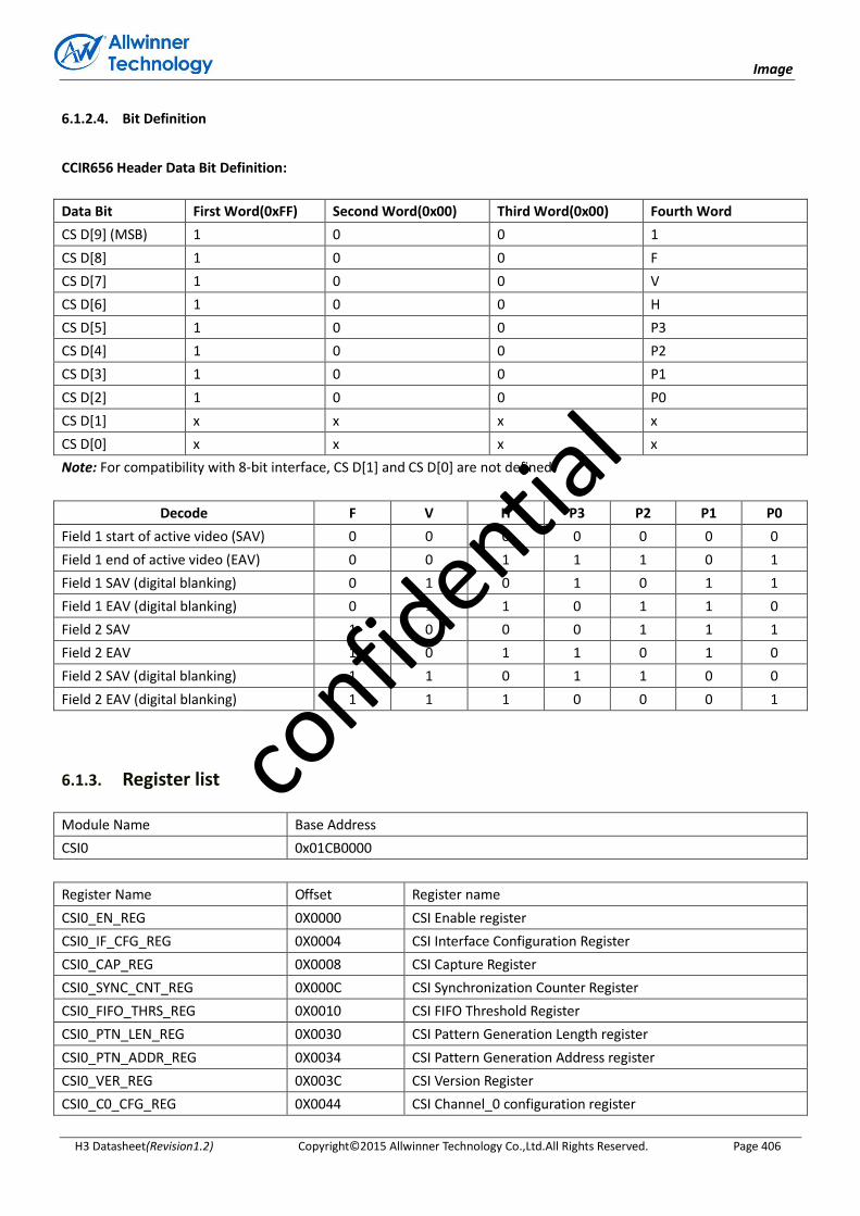
Image
H3 Datasheet(Revision1.2) Copyright© 2015 Allwinner Technology Co.,Ltd.All Rights Reserved. Page 406
6.1.2.4. Bit Definition
CCIR656 Header Data Bit Definition:
Data Bit First Word(0xFF) Second Word(0x00) Third Word(0x00) Fourth Word
CS D[9] (MSB) 1 0 0 1
CS D[8] 1 0 0 F
CS D[7] 1 0 0 V
CS D[6] 1 0 0 H
CS D[5] 1 0 0 P3
CS D[4] 1 0 0 P2
CS D[3] 1 0 0 P1
CS D[2] 1 0 0 P0
CS D[1] x x x x
CS D[0] x x x x
Note: For compatibility with 8-bit interface, CS D[1] and CS D[0] are not defined.
Decode F V H P3 P2 P1 P0
Field 1 start of active video (SAV) 0 0 0 0 0 0 0
Field 1 end of active video (EAV) 0 0 1 1 1 0 1
Field 1 SAV (digital blanking) 0 1 0 1 0 1 1
Field 1 EAV (digital blanking) 0 1 1 0 1 1 0
Field 2 SAV 1 0 0 0 1 1 1
Field 2 EAV 1 0 1 1 0 1 0
Field 2 SAV (digital blanking) 1 1 0 1 1 0 0
Field 2 EAV (digital blanking) 1 1 1 0 0 0 1
6.1.3. Register list
Module Name Base Address
CSI0 0x01CB0000
Register Name Offset Register name
CSI0_EN_REG 0X0000 CSI Enable register
CSI0_IF_CFG_REG 0X0004 CSI Interface Configuration Register
CSI0_CAP_REG 0X0008 CSI Capture Register
CSI0_SYNC_CNT_REG 0X000C CSI Synchronization Counter Register
CSI0_FIFO_THRS_REG 0X0010 CSI FIFO Threshold Register
CSI0_PTN_LEN_REG 0X0030 CSI Pattern Generation Length register
CSI0_PTN_ADDR_REG 0X0034 CSI Pattern Generation Address register
CSI0_VER_REG 0X003C CSI Version Register
CSI0_C0_CFG_REG 0X0044 CSI Channel_0 configuration register
confid
ential

Image
H3 Datasheet(Revision1.2) Copyright© 2015 Allwinner Technology Co.,Ltd.All Rights Reserved. Page 407
CSI0_C0_SCALE_REG 0X004C CSI Channel_0 scale register
CSI0_C0_F0_BUFA_REG 0X0050 CSI Channel_0 FIFO 0 output buffer-A address register
CSI0_C0_F1_BUFA_REG 0X0058 CSI Channel_0 FIFO 1 output buffer-A address register
CSI0_C0_F2_BUFA_REG 0X0060 CSI Channel_0 FIFO 2 output buffer-A address register
CSI0_C0_CAP_STA_REG 0X006C CSI Channel_0 status register
CSI0_C0_INT_EN_REG 0X0070 CSI Channel_0 interrupt enable register
CSI0_C0_INT_STA_REG 0X0074 CSI Channel_0 interrupt status register
CSI0_C0_HSIZE_REG 0X0080 CSI Channel_0 horizontal size register
CSI0_C0_VSIZE_REG 0X0084 CSI Channel_0 vertical size register
CSI0_C0_BUF_LEN_REG 0X0088 CSI Channel_0 line buffer length register
CSI0_C0_FLIP_SIZE_REG 0X008C CSI Channel_0 flip size register
CSI0_C0_FRM_CLK_CNT_REG 0X0090 CSI Channel_0 frame clock counter register
CSI0_C0_ACC_ITNL_CLK_CNT_REG 0X0094 CSI Channel_0 accumulated and internal clock counter register
CSI0_C0_FIFO_STAT_REG 0X0098 CSI Channel_0 FIFO Statistic Register
CSI0_C0_PCLK_STAT_REG 0X009C CSI Channel_0 PCLK Statistic Register
CCI_CTRL 0x3000 CCI control register
CCI_CFG 0x3004 CCI transmission config register
CCI_FMT 0x3008 CCI packet format register
CCI_BUS_CTRL 0x300C CCI bus control register
CCI_INT_CTRL 0x3014 CCI interrupt control register
CCI_LC_TRIG 0x3018 CCI line counter trigger register
CCI_FIFO_ACC 0x3100 CCI FIFO access register
CCI_RSV_REG 0x3200 CCI reserved register
6.1.4. Register Description
6.1.4.1. CSI Enable Register (Default Value: 0x00000000)
Offset: 0x0000 Register Name: CSI0_EN_REG
Bit R/W Default/Hex Description
31 / / /
30 R/W 0x0 VER_EN
CSI Version Register Read Enable:
0: Disable
1: Enable
29:24 / / /
23:16 R/W 0x00 PTN_CYCLE
Pattern generating cycle counter.
The pattern in dram will be generated in cycles of PTN_CYCLE+1.
15:9 / / /
8 R/W 0x0 SRAM_PWDN
0: SRAM in normal
confid
ential

Image
H3 Datasheet(Revision1.2) Copyright© 2015 Allwinner Technology Co.,Ltd.All Rights Reserved. Page 408
1: SRAM in power down
7:5 / / /
4 R/W 0x0 PTN_START
CSI Pattern Generating Start
0: Finish
other: Start
Software write this bit to“1” to start pattern generating from DRAM. When
finished, the hardware will clear this bit to“0”automatically. Generating
cycles depends on PTN_CYCLE.
3 R/W 0 CLK_CNT_SPL
Sampling time for clk counter per frame
0: Sampling clock counter every frame done
1: Sampling clock counter every vsync
2 R/W 0 CLK_CNT_EN
clk count per frame enable
1 R/W 0 PTN_GEN_EN
Pattern Generation Enable
0 R/W 0 CSI_EN
Enable
0: Reset and disable the CSI module
1: Enable the CSI module
6.1.4.2. CSI Interface Configuration Register (Default Value: 0x00000000)
Offset: 0x0004 Register Name: CSI0_IF_CFG_REG
Bit R/W Default/Hex Description
31:22 / / /
21 R/W 0 SRC_TYPE
Source type
0: Progressed
1: Interlaced
20 R/W 0 FPS_DS
Fps down sample
0: no down sample
1: 1/2 fps, only receives the first frame every 2 frames
19 R/W 0 FIELD
For YUV HV timing, Field polarity
0: negative(field=0 indicate odd, field=1 indicate even )
1: positive(field=1 indicate odd, field=0 indicate even )
For BT656 timing, Field sequence
0: Normal sequence (field 0 first)
1: Inverse sequence (field 1 first)
18 R/W 1 VREF_POL
Vref polarity
confid
ential

Image
H3 Datasheet(Revision1.2) Copyright© 2015 Allwinner Technology Co.,Ltd.All Rights Reserved. Page 409
0: negative
1: positive
This register is not apply to CCIR656 interface.
17 R/W 0 HERF_POL
Href polarity
0: negative
1: positive
This register is not apply to CCIR656 interface.
16 R/W 1 CLK_POL
Data clock type
0: active in rising edge
1: active in falling edge
15:12 / / /
11:10 R/W 0 SEQ_8PLUS2
When select IF_DATA_WIDTH to be 8+2bit, odd/even pixel byte at
CSI-D[11:4] will be rearranged to D[11:2]+2’b0 at the actual csi data bus
according to these sequences:
00: 6’bx+D[9:8], D[7:0]
01: D[9:2], 6’bx+D[1:0]
10: D[7:0], D[9:8]+6’bx
11: D[7:0], 6’bx+D[9:8]
9:8 R/W 0 IF_DATA_WIDTH
00: 8 bit data bus
01: 10 bit data bus
10: 12 bit data bus
11: 8+2bit data bus
7:5 / / /
4:0 R/W 0 CSI_IF
YUV:
00000: YUYV422 Interleaved or RAW (All data in one data bus)
CCIR656:
00100: YUYV422 Interleaved or RAW (All data in one data bus)
Others: Reserved
6.1.4.3. CSI Capture Register (Default Value: 0x00000000)
Offset: 0x0008 Register Name: CSI0_CAP_REG
Bit R/W Default/Hex Description
31:6 / / /
5:2 R/W 0x0 CH0_CAP_MASK
Vsync number masked before capture.
1 R/W 0x0 CH0_VCAP_ON
Video capture control: Capture the video image data stream on channel 0.
0: Disable video capture
confid
ential

Image
H3 Datasheet(Revision1.2) Copyright© 2015 Allwinner Technology Co.,Ltd.All Rights Reserved. Page 410
If video capture is in progress, the CSI stops capturing image data at the end
of the current frame, and all of the current frame data is wrote to output
FIFO.
1: Enable video capture
The CSI starts capturing image data at the start of the next frame.
0 R/W 0x0 CH0_SCAP_ON
Still capture control: Capture a single still image frame on channel 0.
0: Disable still capture.
1: Enable still capture
The CSI module starts capturing image data at the start of the next frame.
The CSI module captures only one frame of image data. This bit is self
clearing and always reads as a 0.
6.1.4.4. CSI Synchronization Counter Register (Default Value: 0x00000000)
Offset: 0x000C Register Name: CSI0_SYNC_CNT_REG
Bit R/W Default/Hex Description
31:24 / / /
23:0 R 0 SYNC_CNT
The counter value between vsync of CSI0 channel 0 and vsync of CSI1
channel 0 , using 24MHz.
6.1.4.5. CSI FIFO Threshold Register (Default Value: 0x040f0400)
Offset: 0x0010 Register Name: CSI0_FIFO_THRS_REG
Bit R/W Default/Hex Description
31:29 / / /
28:26 R/W 0x1
FIFO_NEARLY_FULL_TH
The threshold of FIFO being nearly full. Indicates that the ISP should stop
writing. Only valid when ISP is enabled.
0~7:
The smaller the value, the flag of FIFO being nearly full is easier to reach.
25:24 R/W 0x0 PTN_GEN_CLK_DIV
Packet generator clock divider
23:16 R/W 0x0f PTN_GEN_DLY
Clocks delayed before pattern generating start.
15:12 / / /
11:00 R/W 0x400 FIFO_THRS
When CSI0 FIFO occupied memory exceed the threshold, dram frequency
can not change.
confid
ential
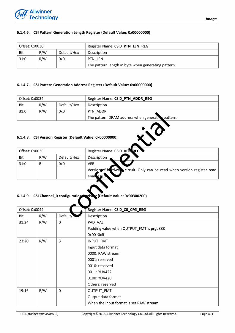
Image
H3 Datasheet(Revision1.2) Copyright© 2015 Allwinner Technology Co.,Ltd.All Rights Reserved. Page 411
6.1.4.6. CSI Pattern Generation Length Register (Default Value: 0x00000000)
Offset: 0x0030 Register Name: CSI0_PTN_LEN_REG
Bit R/W Default/Hex Description
31:0 R/W 0x0 PTN_LEN
The pattern length in byte when generating pattern.
6.1.4.7. CSI Pattern Generation Address Register (Default Value: 0x00000000)
Offset: 0x0034 Register Name: CSI0_PTN_ADDR_REG
Bit R/W Default/Hex Description
31:0 R/W 0x0 PTN_ADDR
The pattern DRAM address when generating pattern.
6.1.4.8. CSI Version Register (Default Value: 0x00000000)
Offset: 0x003C Register Name: CSI0_VER_REG
Bit R/W Default/Hex Description
31:0 R 0x0 VER
Version of hardware circuit. Only can be read when version register read
enable is on.
6.1.4.9. CSI Channel_0 configuration Register (Default Value: 0x00300200)
Offset: 0x0044 Register Name: CSI0_C0_CFG_REG
Bit R/W Default/Hex Description
31:24 R/W 0 PAD_VAL
Padding value when OUTPUT_FMT is prgb888
0x00~0xff
23:20 R/W 3 INPUT_FMT
Input data format
0000: RAW stream
0001: reserved
0010: reserved
0011: YUV422
0100: YUV420
Others: reserved
19:16 R/W 0 OUTPUT_FMT
Output data format
When the input format is set RAW stream
confid
ential

Image
H3 Datasheet(Revision1.2) Copyright© 2015 Allwinner Technology Co.,Ltd.All Rights Reserved. Page 412
0000: field-raw-8
0001: field-raw-10
0010: field-raw-12
0011: reserved
0100: field-rgb565
0101: field-rgb888
0110: field-prgb888
1000: frame-raw-8
1001: frame-raw-10
1010: frame-raw-12
1011: reserved
1100: frame-rgb565
1101: frame-rgb888
1110: frame-prgb888
When the input format is set YUV422
0000: field planar YCbCr 422
0001: field planar YCbCr 420
0010: frame planar YCbCr 420
0011: frame planar YCbCr 422
0100: field planar YCbCr 422 UV combined
0101: field planar YCbCr 420 UV combined
0110: frame planar YCbCr 420 UV combined
0111: frame planar YCbCr 422 UV combined
1000: field MB YCbCr 422
1001: field MB YCbCr 420
1010: frame MB YCbCr 420
1011: frame MB YCbCr 422
1100: field planar YCbCr 422 10bit UV combined
1101: field planar YCbCr 420 10bit UV combined
1110: Reserved
1111: Reserved
When the input format is set YUV420
0000: Reserved
0001: field planar YCbCr 420
0010: frame planar YCbCr 420
0011: Reserved
0100: Reserved
0101: field planar YCbCr 420 UV combined
0110: frame planar YCbCr 420 UV combined
0111: Reserved
1000: Reserved
1001: field MB YCbCr 420
1010: frame MB YCbCr 420
confid
ential
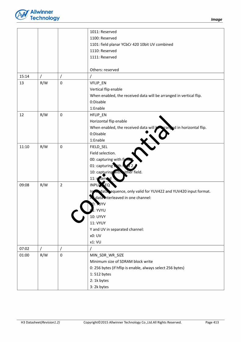
Image
H3 Datasheet(Revision1.2) Copyright© 2015 Allwinner Technology Co.,Ltd.All Rights Reserved. Page 413
1011: Reserved
1100: Reserved
1101: field planar YCbCr 420 10bit UV combined
1110: Reserved
1111: Reserved
Others: reserved
15:14 / / /
13 R/W 0 VFLIP_EN
Vertical flip enable
When enabled, the received data will be arranged in vertical flip.
0:Disable
1:Enable
12 R/W 0 HFLIP_EN
Horizontal flip enable
When enabled, the received data will be arranged in horizontal flip.
0:Disable
1:Enable
11:10 R/W 0 FIELD_SEL
Field selection.
00: capturing with field 1.
01: capturing with field 2.
10: capturing with either field.
11: reserved
09:08 R/W 2 INPUT_SEQ
Input data sequence, only valid for YUV422 and YUV420 input format.
All data interleaved in one channel:
00: YUYV
01: YVYU
10: UYVY
11: VYUY
Y and UV in separated channel:
x0: UV
x1: VU
07:02 / / /
01:00 R/W 0 MIN_SDR_WR_SIZE
Minimum size of SDRAM block write
0: 256 bytes (if hflip is enable, always select 256 bytes)
1: 512 bytes
2: 1k bytes
3: 2k bytes
confid
ential
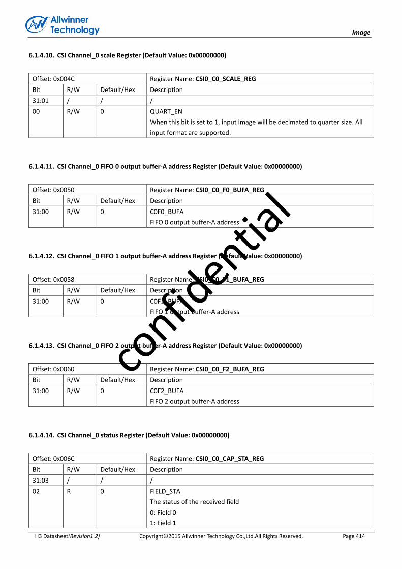
Image
H3 Datasheet(Revision1.2) Copyright© 2015 Allwinner Technology Co.,Ltd.All Rights Reserved. Page 414
6.1.4.10. CSI Channel_0 scale Register (Default Value: 0x00000000)
Offset: 0x004C Register Name: CSI0_C0_SCALE_REG
Bit R/W Default/Hex Description
31:01 / / /
00 R/W 0 QUART_EN
When this bit is set to 1, input image will be decimated to quarter size. All
input format are supported.
6.1.4.11. CSI Channel_0 FIFO 0 output buffer-A address Register (Default Value: 0x00000000)
Offset: 0x0050 Register Name: CSI0_C0_F0_BUFA_REG
Bit R/W Default/Hex Description
31:00 R/W 0 C0F0_BUFA
FIFO 0 output buffer-A address
6.1.4.12. CSI Channel_0 FIFO 1 output buffer-A address Register (Default Value: 0x00000000)
Offset: 0x0058 Register Name: CSI0_C0_F1_BUFA_REG
Bit R/W Default/Hex Description
31:00 R/W 0 C0F1_BUFA
FIFO 1 output buffer-A address
6.1.4.13. CSI Channel_0 FIFO 2 output buffer-A address Register (Default Value: 0x00000000)
Offset: 0x0060 Register Name: CSI0_C0_F2_BUFA_REG
Bit R/W Default/Hex Description
31:00 R/W 0 C0F2_BUFA
FIFO 2 output buffer-A address
6.1.4.14. CSI Channel_0 status Register (Default Value: 0x00000000)
Offset: 0x006C Register Name: CSI0_C0_CAP_STA_REG
Bit R/W Default/Hex Description
31:03 / / /
02 R 0 FIELD_STA
The status of the received field
0: Field 0
1: Field 1
confid
ential
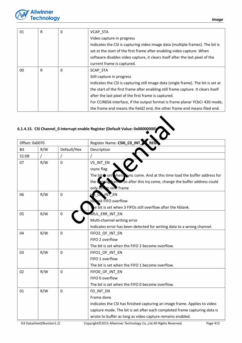
Image
H3 Datasheet(Revision1.2) Copyright© 2015 Allwinner Technology Co.,Ltd.All Rights Reserved. Page 415
01 R 0 VCAP_STA
Video capture in progress
Indicates the CSI is capturing video image data (multiple frames). The bit is
set at the start of the first frame after enabling video capture. When
software disables video capture, it clears itself after the last pixel of the
current frame is captured.
00 R 0 SCAP_STA
Still capture in progress
Indicates the CSI is capturing still image data (single frame). The bit is set at
the start of the first frame after enabling still frame capture. It clears itself
after the last pixel of the first frame is captured.
For CCIR656 interface, if the output format is frame planar YCbCr 420 mode,
the frame end means the field2 end, the other frame end means filed end.
6.1.4.15. CSI Channel_0 interrupt enable Register (Default Value: 0x00000000)
Offset: 0x0070 Register Name: CSI0_C0_INT_EN_REG
Bit R/W Default/Hex Description
31:08 / / /
07 R/W 0 VS_INT_EN
vsync flag
The bit is set when vsync come. And at this time load the buffer address for
the coming frame. So after this irq come, change the buffer address could
only effect next frame
06 R/W 0 HB_OF_INT_EN
Hblank FIFO overflow
The bit is set when 3 FIFOs still overflow after the hblank.
05 R/W 0 MUL_ERR_INT_EN
Multi-channel writing error
Indicates error has been detected for writing data to a wrong channel.
04 R/W 0 FIFO2_OF_INT_EN
FIFO 2 overflow
The bit is set when the FIFO 2 become overflow.
03 R/W 0 FIFO1_OF_INT_EN
FIFO 1 overflow
The bit is set when the FIFO 1 become overflow.
02 R/W 0 FIFO0_OF_INT_EN
FIFO 0 overflow
The bit is set when the FIFO 0 become overflow.
01 R/W 0 FD_INT_EN
Frame done
Indicates the CSI has finished capturing an image frame. Applies to video
capture mode. The bit is set after each completed frame capturing data is
wrote to buffer as long as video capture remains enabled.
confid
ential

Image
H3 Datasheet(Revision1.2) Copyright© 2015 Allwinner Technology Co.,Ltd.All Rights Reserved. Page 416
00 R/W 0 CD_INT_EN
Capture done
Indicates the CSI has completed capturing the image data.
For still capture, the bit is set when one frame data has been wrote to
buffer.
For video capture, the bit is set when the last frame has been wrote to
buffer after video capture has been disabled.
For CCIR656 interface, if the output format is frame planar YCbCr 420 mode,
the frame end means the field2 end, the other frame end means field end.
6.1.4.16. CSI Channel_0 interrupt status Register (Default Value: 0x00000000)
Offset: 0x0074 Register Name: CSI0_C0_INT_STA_REG
Bit R/W Default/Hex Description
31:08 / / /
07 R/W 0 VS_PD
vsync flag
06 R/W 0 HB_OF_PD
Hblank FIFO overflow
05 R/W 0 MUL_ ERR_PD
Multi-channel writing error
04 R/W 0 FIFO2_OF_PD
FIFO 2 overflow
03 R/W 0 FIFO1_OF_PD
FIFO 1 overflow
02 R/W 0 FIFO0_OF_PD
FIFO 0 overflow
01 R/W 0 FD_PD
Frame done
00 R/W 0 CD_PD
Capture done
6.1.4.17. CSI Channel_0 horizontal size Register (Default Value: 0x05000000)
Offset: 0x0080 Register Name: CSI0_C0_INT_STA_REG
Bit R/W Default/Hex Description
31:29 / / /
28:16 R/W 500 HOR_LEN
Horizontal pixel unit length. Valid pixel of a line.
15:13 / / /
12:00 R/W 0 HOR_START
Horizontal pixel unit start. Pixel is valid from this pixel.
confid
ential

Image
H3 Datasheet(Revision1.2) Copyright© 2015 Allwinner Technology Co.,Ltd.All Rights Reserved. Page 417
6.1.4.18. CSI Channel_0 vertical size Register (Default Value: 0x01E00000)
Offset: 0x0084 Register Name: CSI0_C0_VSIZE_REG
Bit R/W Default/Hex Description
31:29 / / /
28:16 R/W 1E0 VER_LEN
Vertical line length. Valid line number of a frame.
15:13 / / /
12:00 R/W 0 VER_START
Vertical line start. data is valid from this line.
6.1.4.19. CSI Channel_0 buffer length Register (Default Value: 0x01400280)
Offset: 0x0088 Register Name: CSI0_C0_BUF_LEN_REG
Bit R/W Default/Hex Description
31:30 / / /
29:16 R/W 140 BUF_LEN_C
Buffer length of chroma C in a line. Unit is byte.
15:14 / / /
13:00 R/W 280 BUF_LEN
Buffer length of luminance Y in a line. Unit is byte.
6.1.4.20. CSI Channel_0 flip size Register (Default Value: 0x01E00280)
Offset: 0x008C Register Name: CSI0_C0_FLIP_SIZE_REG
Bit R/W Default/Hex Description
31:29 / / /
28:16 R/W 1E0 VER_LEN
Vertical line number when in vflip mode.
15:13 / / /
12:00 R/W 280 VALID_LEN
Valid components of a line when in flip mode.
6.1.4.21. CSI Channel_0 frame clock counter Register (Default Value: 0x00000000)
Offset: 0x0090 Register Name: CSI0_C0_FRM_CLK_CNT_REG
Bit R/W Default/Hex Description
31:24 / / /
confid
ential
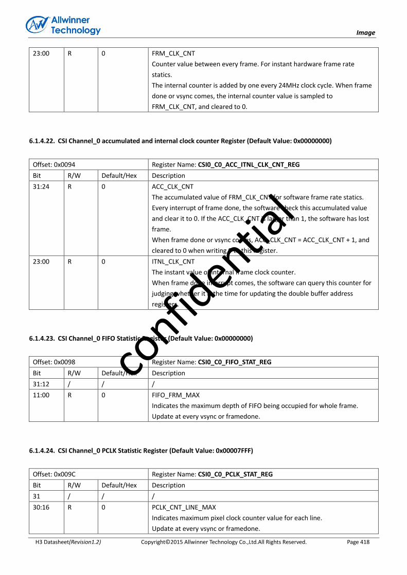
Image
H3 Datasheet(Revision1.2) Copyright© 2015 Allwinner Technology Co.,Ltd.All Rights Reserved. Page 418
23:00 R 0 FRM_CLK_CNT
Counter value between every frame. For instant hardware frame rate
statics.
The internal counter is added by one every 24MHz clock cycle. When frame
done or vsync comes, the internal counter value is sampled to
FRM_CLK_CNT, and cleared to 0.
6.1.4.22. CSI Channel_0 accumulated and internal clock counter Register (Default Value: 0x00000000)
Offset: 0x0094 Register Name: CSI0_C0_ACC_ITNL_CLK_CNT_REG
Bit R/W Default/Hex Description
31:24 R 0 ACC_CLK_CNT
The accumulated value of FRM_CLK_CNT for software frame rate statics.
Every interrupt of frame done, the software check this accumulated value
and clear it to 0. If the ACC_CLK_CNT is larger than 1, the software has lost
frame.
When frame done or vsync comes, ACC_CLK_CNT = ACC_CLK_CNT + 1, and
cleared to 0 when writing 0 to this register.
23:00 R 0 ITNL_CLK_CNT
The instant value of internal frame clock counter.
When frame done interrupt comes, the software can query this counter for
judging whether it is the time for updating the double buffer address
registers.
6.1.4.23. CSI Channel_0 FIFO Statistic Register (Default Value: 0x00000000)
Offset: 0x0098 Register Name: CSI0_C0_FIFO_STAT_REG
Bit R/W Default/Hex Description
31:12 / / /
11:00 R 0 FIFO_FRM_MAX
Indicates the maximum depth of FIFO being occupied for whole frame.
Update at every vsync or framedone.
6.1.4.24. CSI Channel_0 PCLK Statistic Register (Default Value: 0x00007FFF)
Offset: 0x009C Register Name: CSI0_C0_PCLK_STAT_REG
Bit R/W Default/Hex Description
31 / / /
30:16 R 0 PCLK_CNT_LINE_MAX
Indicates maximum pixel clock counter value for each line.
Update at every vsync or framedone.
confid
ential

Image
H3 Datasheet(Revision1.2) Copyright© 2015 Allwinner Technology Co.,Ltd.All Rights Reserved. Page 419
15 / / /
14:00 R 0x7fff PCLK_CNT_LINE_MIN
Indicates minimum pixel clock counter value for each line.
Update at every vsync or framedone.
6.1.4.25. CCI Control Register (Default Value: 0x00000000)
Offset: 0x3000 Register Name: CCI_CTRL_REG
Bit R/W Default/Hex Description
31 R/W 0 SINGLE_TRAN
0: Transmission idle
1: Start single transmission
Automatically cleared to ‘0’ when finished. Abort current transmission
immediately if changing from ‘1’ to ‘0’. If slave not respond for the expected
status over the time defined by TIMEOUT, current transmission will stop.
PACKET_CNT will return the sequence number when transmission fail. All
format setting and data will be loaded from registers and FIFO when
transmission start.
30 R/W 0 REPEAT_TRAN
0: transmission idle
1: repeated transmission
When this bit is set to 1, transmission repeats when trigger signal (such as
VSYNC/ VCAP done ) repeats.
If changing this bit from ‘1’ to ‘0’ during transmission, the current
transmission will be guaranteed then stop.
29 R/W 0 RESTART_MODE
0: RESTART
1: STOP+START
Define the CCI action after sending register address.
28 R/W 0 READ_TRAN_MODE
0: send slave_id+W
1: do not send slave_id+W
Note:Setting this bit to 1 if reading from a slave which register width is
equal to 0.
27:24 R 0 TRAN_RESULT
000: OK
001: FAIL
Other: Reserved
23:16 R / CCI_STA
0x00: bus error
0x08: START condition transmitted
0x10: Repeated START condition transmitted
0x18: Address + Write bit transmitted, ACK received
0x20: Address + Write bit transmitted, ACK not received
confid
ential

Image
H3 Datasheet(Revision1.2) Copyright© 2015 Allwinner Technology Co.,Ltd.All Rights Reserved. Page 420
0x28: Data byte transmitted in master mode, ACK received
0x30: Data byte transmitted in master mode, ACK not received
0x38: Arbitration lost in address or data byte
0x40: Address + Read bit transmitted, ACK received
0x48: Address + Read bit transmitted, ACK not received
0x50: Data byte received in master mode, ACK received
0x58: Data byte received in master mode, ACK not received
0x01: Timeout when sending 9th SCL clk
Other: Reserved
15:2 / / /
1 R/W 0 SOFT_RESET
0: normal
1: reset
0 R/W 0 CCI_EN
0: Module disable
1: Module enable
6.1.4.26. CCI Transmission Configuration Register (Default Value: 0x10000000)
Offset: 0x3004 Register Name: CCI_CFG_REG
Bit R/W Default/Hex Description
31:24 R/W 0x10 TIMEOUT_N
When sending the 9th clock, assert fail signal when slave device did not
response after N*FSCL cycles. And software must do a reset to CCI module
and send a stop condition to slave.
23:16 R/W 0x00 INTERVAL
Define the interval between each packet in 40*FSCL cycles. 0~255
15 R/W 0 PACKET_MODE
Select where to load slave id / data width
0: Compact mode
1: Complete mode
In compact mode, slave id/register width / data width will be loaded from
CCI_FMT register, only address and data read from memory.
In complete mode, they will be loaded from packet memory.
14:7 / / /
6:4 R/W 0 TRIG_MODE
Transmit mode:
000: Immediately, no trigger
001: Reserved
010: CSI0 int trigger
011: CSI1 int trigger
3:0 R/W 0 CSI_TRIG
CSI Int trig signal select:
0000: First HREF start
confid
ential

Image
H3 Datasheet(Revision1.2) Copyright© 2015 Allwinner Technology Co.,Ltd.All Rights Reserved. Page 421
0001: Last HREF done
0010: Line counter trigger
other: Reserved
6.1.4.27. CCI Packet Format Register (Default Value: 0x00110001)
Offset: 0x3008 Register Name: CCI_FMT_REG
Bit R/W Default/Hex Description
31:25 R/W 0 SLV_ID
7bit address
24 R/W 0 CMD
0: write
1: read
23:20 R/W 1 ADDR_BYTE
How many bytes be sent as address
0~15
19:16 R/W 1 DATA_BYTE
How many bytes be sent/received as data
1~15
Normally use ADDR_DATA with 0_2, 1_1, 1_2, 2_1, 2_2 access mode. If
DATA bytes is 0, transmission will not start. In complete mode, the
ADDR_BYTE and DATA_BYTE is defined in a byte’s high/low 4bit.
15:0 R/W 1 PACKET_CNT
FIFO data be transmitted as PACKET_CNT packets in current format.
Total bytes not exceed 32bytes.
6.1.4.28. CCI Bus Control Register (Default Value: 0x00002500)
Offset: 0x300C Register Name: CCI_BUS_REG
Bit R/W Default/Hex Description
31:16 R/W 0 DLY_CYC
0~65535 FSCL cycles between each transmission
15 R/W 0 DLY_TRIG
0: disable
1: execute transmission after internal counter delay when triggered
14:12 R/W 0x2 CLK_N
CCI bus sampling clock F0=24MHz/2^CLK_N
11:8 R/W 0x5 CLK_M
CCI output SCL frequency is FSCL=F1/10=(F0/(CLK_M+1))/10
7 R / SCL_STA
SCL current status
6 R / SDA_STA
confid
ential
Image
H3 Datasheet(Revision1.2) Copyright© 2015 Allwinner Technology Co.,Ltd.All Rights Reserved. Page 422
SDA current status
5 R/W 0 SCL_PEN
SCL PAD enable
4 R/W 0 SDA_PEN
SDA PAD enable
3 R/W 0 SCL_MOV
SCL manual output value
2 R/W 0 SDA_MOV
SDA manual output value
1 R/W 0 SCL_MOE
SCL manual output en
0 R/W 0 SDA_MOE
SDA manual output en
6.1.4.29. CCI Interrupt Control Register (Default Value: 0x00000000)
Offset: 0x3014 Register Name: CCI_INT_CTRL_REG
Bit R/W Default/Hex Description
31:18 / / /
17 R/W 0 S_TRAN_ERR_INT_EN
16 R/W 0 S_TRAN_COM_INT_EN
15:2 / / /
1 R/W 0 S_TRAN_ERR_PD
0 R/W 0 S_TRAN_COM_PD
6.1.4.30. CCI Line Counter Trigger Control Register (Default Value: 0x00000000)
Offset: 0x3018 Register Name: CCI_LC_REG
Bit R/W Default/Hex Description
31:13 / / /
12:0 R/W 0 LN_CNT
0~8191: line counter send trigger when 1st~8192th line is received.
6.1.4.31. CCI FIFO Acess Register (Default Value: 0x00000000)
Offset: 0x3100~0x313f Register Name: CCI_FIFO_ACC_REG
Bit R/W Default/Hex Description
31:0 R/W 0 DATA_FIFO
From 0x100 to 0x13f, CCI data fifo is 64bytes, used in fifo input mode. CCI
transmission read/write data from/to fifo in byte.
confid
ential
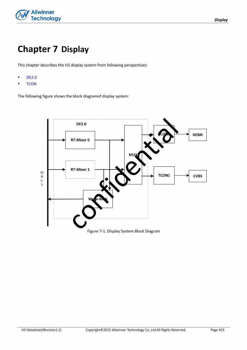
Display
H3 Datasheet(Revision1.2) Copyright© 2015 Allwinner Technology Co.,Ltd.All Rights Reserved. Page 423
Chapter 7 Display
This chapter describes the H3 display system from following perspectives:
DE2.0
TCON
The following figure shows the block diagramof display system:
Figure 7-1. Display System Block Diagram
confid
ential
Display
H3 Datasheet(Revision1.2) Copyright© 2015 Allwinner Technology Co.,Ltd.All Rights Reserved. Page 424
7.1. DE2.0
7.1.1. Overview
Output size up to 4096x4096
Support four alpha blending channel for main display, two channel for aux display
Support four overlay layers in each channel, and has a independent scaler
Support potter-duff compatible blending operation
Support input format YUV422/YUV420/YUV411/ARGB8888/XRGB8888/RGB888/ARGB4444/ARGB1555 and
RGB565
Support Frame Packing/Top-and-Bottom/Side-by-side Full/Side-by-Side Half 3D format data
Support SmartColor 2.0 for excellent display experience
- Adaptive edge sharping
- Adaptive color enhancement
- Adaptive contrast enhancement and fresh tone rectify
Support writeback for high efficient dual display
confid
ential

Display
H3 Datasheet(Revision1.2) Copyright© 2015 Allwinner Technology Co.,Ltd.All Rights Reserved. Page 425
7.2. TCON
7.2.1. Overview
The LCD0 module is used for HDMI, and LCD1 module is used for TV.
Support HDMI interface, up to 4K
Support TV interface, up to 480P/576P
2 interrupts for programmer single TCON output
7.2.2. Block Diagram
Figure 7-2. TCON Block Diagram
7.2.3. Functionalities Description
7.2.3.1. RGB gamma correction
Function: This module correct the RGB input data of DE0 .
A 256*8*3 Byte register file is used to store the gamma table. The following is the layout:
Offset Value
0x400, 0x401, 0x402 { B0[7:0], G0[7:0], R0[7:0] }
0x404, { B1[7:0], G1[7:0], R1[7:0] }
confid
ential
Display
H3 Datasheet(Revision1.2) Copyright© 2015 Allwinner Technology Co.,Ltd.All Rights Reserved. Page 426
...... ......
0x4FC { B255[7:0], G255[7:0], R255[7:0] }
7.2.3.2. CEU module
Function: This module enhance color data from DE0 .
R’ = Rr*R + Rg*G + Rb*B + Rc
G’ = Gr*R + Gg*G + Gb*B +Gc
B’ = Br*R + Bg*G + Bb*B + Bc
Note:
Rr, Rg, Rb, ,Gr, Gg, Gb, Br, Bg, Bb s13 (-16,16)
Rc, Gc, Bc s19 (-16384, 16384)
R, G, B u8 [0-255]
R’ have the range of [Rmin ,Rmax]
G’ have the range of [Rmin ,Rmax]
B’ have the range of [Rmin ,Rmax]
7.2.4. LCD0 Module Register List
Module Name Base Address
TCON0 0x01C0C000
Register Name Offset Description
TCON_GCTL_REG 0x000 TCON global control register
TCON_GINT0_REG 0x004 TCON global interrupt register0
TCON_GINT1_REG 0x008 TCON global interrupt register1
TCON1_CTL_REG 0x090 TCON1 control register
TCON1_BASIC0_REG 0x094 TCON1 basic timing register0
TCON1_BASIC1_REG 0x098 TCON1 basic timing register1
TCON1_BASIC2_REG 0x09C TCON1 basic timing register2
TCON1_BASIC3_REG 0x0A0 TCON1 basic timing register3
TCON1_BASIC4_REG 0x0A4 TCON1 basic timing register4
TCON1_BASIC5_REG 0x0A8 TCON1 basic timing register5
TCON1_PS_SYNC_REG 0x0B0 TCON1 sync register
TCON1_IO_POL_REG 0x0F0 TCON1 IO polarity register
TCON1_IO_TRI_REG 0x0F4 TCON1 IO control register
TCON_ECC_FIFO_REG 0x0F8 TCON ECC FIFO register
TCON_CEU_CTL_REG 0x100 TCON CEU control register
TCON_CEU_COEF_MUL_REG 0x110+N*0x04 TCON CEU coefficient register0
(N=0,1,2,4,5,6,8,9,10)
TCON_CEU_COEF_ADD_REG 0x11C+N*0x10 TCON CEU coefficient register1
(N=0,1,2)
confid
ential

Display
H3 Datasheet(Revision1.2) Copyright© 2015 Allwinner Technology Co.,Ltd.All Rights Reserved. Page 427
TCON_CEU_COEF_RANG_REG 0x140+N*0x04 TCON CEU coefficient register2
(N=0,1,2)
TCON_SAFE_PERIOD_REG 0x1F0 TCON safe period register
TCON1_FILL_CTL_REG 0x300 TCON1 fill data control register
TCON1_FILL_BEGIN_REG 0x304+N*0x0C TCON1 fill data begin register
(N=0,1,2)
TCON1_FILL_END_REG 0x308+N*0x0C TCON1 fill data end register
(N=0,1,2)
TCON1_FILL_DATA0_REG 0x30C+N*0x0C TCON1 fill data value register
(N=0,1,2)
TCON1_GAMMA_TABLE_REG 0x400-0x7FF
TCON_ECC_FIFO_BIST_REG 0xFFC
7.2.5. LCD0 Module Register Description
7.2.5.1. TCON Global Control Register (Default Value: 0x00000000)
Offset: 0x0000 Register Name: TCON_GCTL_REG
Bit R/W Default/Hex Description
31 R/W 0 TCON_En
0: disable
1: enable
When it’s disabled, the module will be reset to idle state.
30 R/W 0 TCON_Gamma_En
0: disable
1: enable
29:0 / / /
7.2.5.2. TCON Global Interrupt Register0 (Default Value: 0x00000000)
Offset: 0x0004 Register Name: TCON_GINT0_REG
Bit R/W Default/Hex Description
31 / / /
30 R/W 0 TCON1_Vb_Int_En
0: disable
1: enable
29 / / /
28 R/W 0 TCON1_Line_Int_En
0: disable
1: enable
27:15 / / /
confid
ential
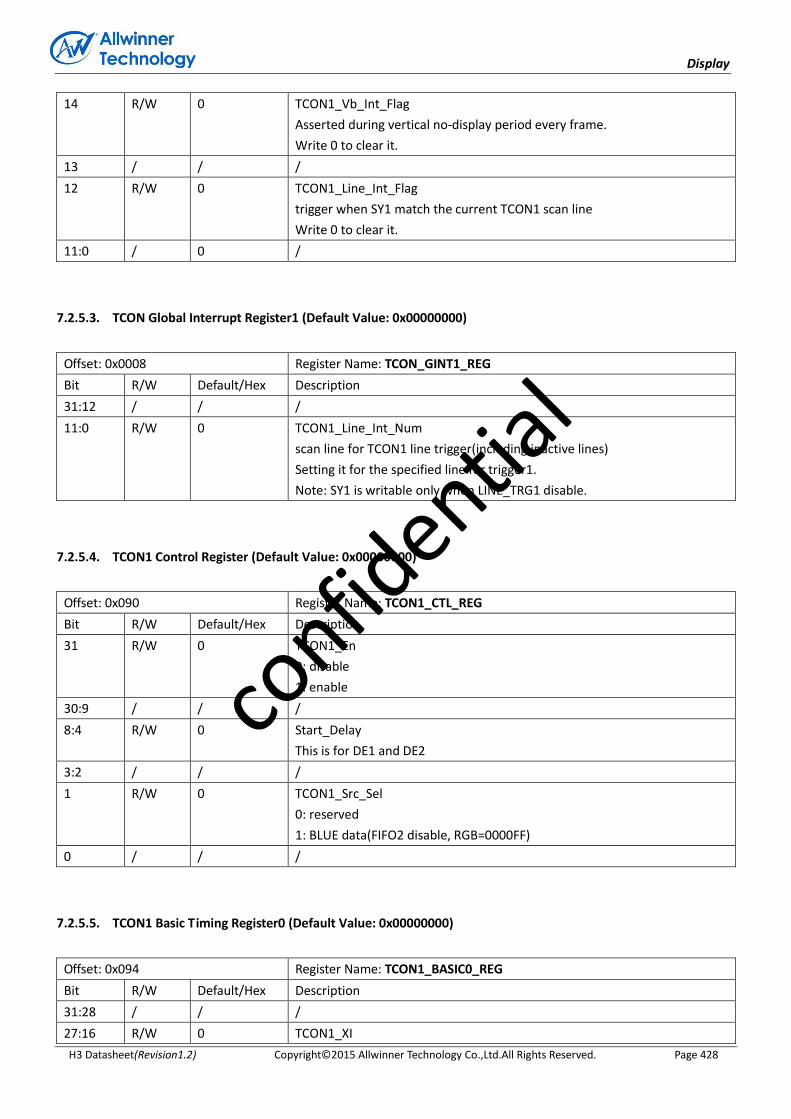
Display
H3 Datasheet(Revision1.2) Copyright© 2015 Allwinner Technology Co.,Ltd.All Rights Reserved. Page 428
14 R/W 0 TCON1_Vb_Int_Flag
Asserted during vertical no-display period every frame.
Write 0 to clear it.
13 / / /
12 R/W 0 TCON1_Line_Int_Flag
trigger when SY1 match the current TCON1 scan line
Write 0 to clear it.
11:0 / 0 /
7.2.5.3. TCON Global Interrupt Register1 (Default Value: 0x00000000)
Offset: 0x0008 Register Name: TCON_GINT1_REG
Bit R/W Default/Hex Description
31:12 / / /
11:0 R/W 0 TCON1_Line_Int_Num
scan line for TCON1 line trigger(including inactive lines)
Setting it for the specified line for trigger1.
Note: SY1 is writable only when LINE_TRG1 disable.
7.2.5.4. TCON1 Control Register (Default Value: 0x00000000)
Offset: 0x090 Register Name: TCON1_CTL_REG
Bit R/W Default/Hex Description
31 R/W 0 TCON1_En
0: disable
1: enable
30:9 / / /
8:4 R/W 0 Start_Delay
This is for DE1 and DE2
3:2 / / /
1 R/W 0 TCON1_Src_Sel
0: reserved
1: BLUE data(FIFO2 disable, RGB=0000FF)
0 / / /
7.2.5.5. TCON1 Basic Timing Register0 (Default Value: 0x00000000)
Offset: 0x094 Register Name: TCON1_BASIC0_REG
Bit R/W Default/Hex Description
31:28 / / /
27:16 R/W 0 TCON1_XI
confid
ential

Display
H3 Datasheet(Revision1.2) Copyright© 2015 Allwinner Technology Co.,Ltd.All Rights Reserved. Page 429
source width is X+1
15:12 / / /
11:0 R/W 0 TCON1_YI
source height is Y+1
7.2.5.6. TCON1 Basic Timing Register1 (Default Value: 0x00000000)
Offset: 0x098 Register Name: TCON1_BASIC1_REG
Bit R/W Default/Hex Description
31:28 / / /
27:16 R/W 0 LS_XO
width is LS_XO+1
15:12 / / /
11:0 R/W 0 LS_YO
width is LS_YO+1
NOTE: This version LS_YO = TCON1_YI
7.2.5.7. TCON1 Basic Timing Register2 (Default Value: 0x00000000)
Offset: 0x09C Register Name: TCON1_BASIC2_REG
Bit R/W Default/Hex Description
31:28 / / /
27:16 R/W 0 TCON1_XO
width is TCON1_XO+1
15:12 / / /
11:0 R/W 0 TCON1_YO
height is TCON1_YO+1
7.2.5.8. TCON1 Basic Timing Register3 (Default Value: 0x00000000)
Offset: 0x0A0 Register Name: TCON1_BASIC3_REG
Bit R/W Default/Hex Description
31:29 / / /
28:16 R/W 0 HT
horizontal total time
Thcycle = (HT+1) * Thdclk
15:12 / / /
11:0 R/W 0 HBP
horizontal back porch
Thbp = (HBP +1) * Thdclk
confid
ential
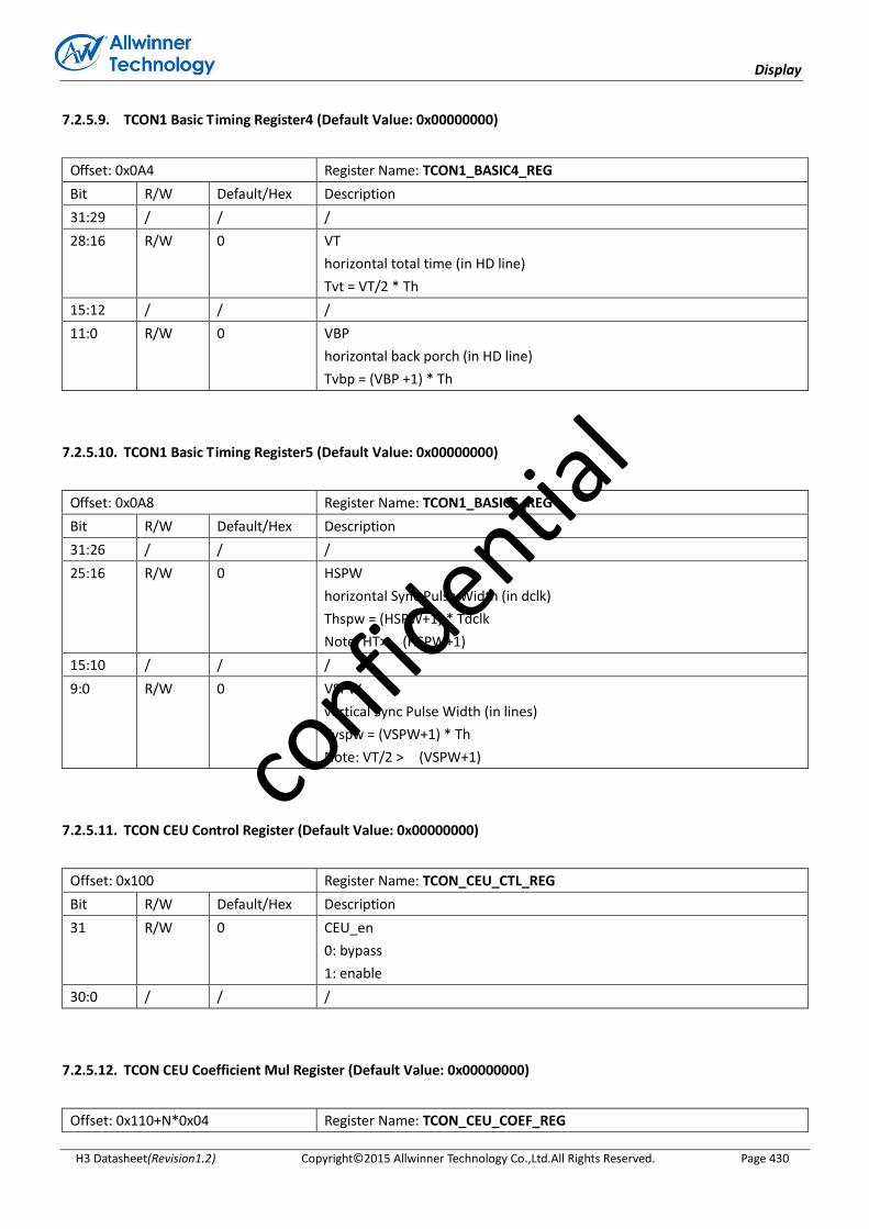
Display
H3 Datasheet(Revision1.2) Copyright© 2015 Allwinner Technology Co.,Ltd.All Rights Reserved. Page 430
7.2.5.9. TCON1 Basic Timing Register4 (Default Value: 0x00000000)
Offset: 0x0A4 Register Name: TCON1_BASIC4_REG
Bit R/W Default/Hex Description
31:29 / / /
28:16 R/W 0 VT
horizontal total time (in HD line)
Tvt = VT/2 * Th
15:12 / / /
11:0 R/W 0 VBP
horizontal back porch (in HD line)
Tvbp = (VBP +1) * Th
7.2.5.10. TCON1 Basic Timing Register5 (Default Value: 0x00000000)
Offset: 0x0A8 Register Name: TCON1_BASIC5_REG
Bit R/W Default/Hex Description
31:26 / / /
25:16 R/W 0 HSPW
horizontal Sync Pulse Width (in dclk)
Thspw = (HSPW+1) * Tdclk
Note: HT> (HSPW+1)
15:10 / / /
9:0 R/W 0 VSPW
vertical Sync Pulse Width (in lines)
Tvspw = (VSPW+1) * Th
Note: VT/2 > (VSPW+1)
7.2.5.11. TCON CEU Control Register (Default Value: 0x00000000)
Offset: 0x100 Register Name: TCON_CEU_CTL_REG
Bit R/W Default/Hex Description
31 R/W 0 CEU_en
0: bypass
1: enable
30:0 / / /
7.2.5.12. TCON CEU Coefficient Mul Register (Default Value: 0x00000000)
Offset: 0x110+N*0x04 Register Name: TCON_CEU_COEF_REG
confid
ential
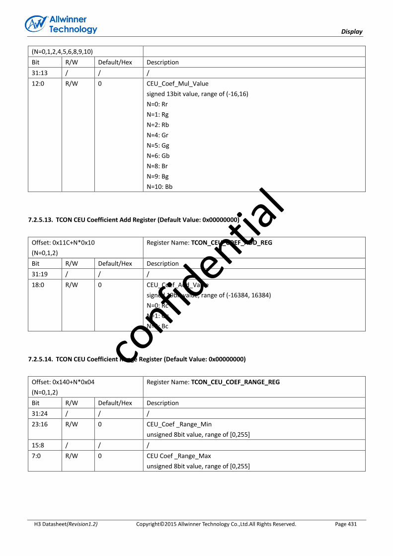
Display
H3 Datasheet(Revision1.2) Copyright© 2015 Allwinner Technology Co.,Ltd.All Rights Reserved. Page 431
(N=0,1,2,4,5,6,8,9,10)
Bit R/W Default/Hex Description
31:13 / / /
12:0 R/W 0 CEU_Coef_Mul_Value
signed 13bit value, range of (-16,16)
N=0: Rr
N=1: Rg
N=2: Rb
N=4: Gr
N=5: Gg
N=6: Gb
N=8: Br
N=9: Bg
N=10: Bb
7.2.5.13. TCON CEU Coefficient Add Register (Default Value: 0x00000000)
Offset: 0x11C+N*0x10
(N=0,1,2)
Register Name: TCON_CEU_COEF_ADD_REG
Bit R/W Default/Hex Description
31:19 / / /
18:0 R/W 0 CEU_Coef_Add_Value
signed 19bit value, range of (-16384, 16384)
N=0: Rc
N=1: Gc
N=2: Bc
7.2.5.14. TCON CEU Coefficient Range Register (Default Value: 0x00000000)
Offset: 0x140+N*0x04
(N=0,1,2)
Register Name: TCON_CEU_COEF_RANGE_REG
Bit R/W Default/Hex Description
31:24 / / /
23:16 R/W 0 CEU_Coef _Range_Min
unsigned 8bit value, range of [0,255]
15:8 / / /
7:0 R/W 0 CEU Coef _Range_Max
unsigned 8bit value, range of [0,255]
confid
ential
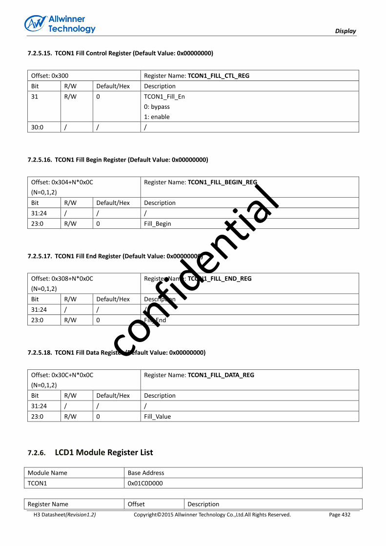
Display
H3 Datasheet(Revision1.2) Copyright© 2015 Allwinner Technology Co.,Ltd.All Rights Reserved. Page 432
7.2.5.15. TCON1 Fill Control Register (Default Value: 0x00000000)
Offset: 0x300 Register Name: TCON1_FILL_CTL_REG
Bit R/W Default/Hex Description
31 R/W 0 TCON1_Fill_En
0: bypass
1: enable
30:0 / / /
7.2.5.16. TCON1 Fill Begin Register (Default Value: 0x00000000)
Offset: 0x304+N*0x0C
(N=0,1,2)
Register Name: TCON1_FILL_BEGIN_REG
Bit R/W Default/Hex Description
31:24 / / /
23:0 R/W 0 Fill_Begin
7.2.5.17. TCON1 Fill End Register (Default Value: 0x00000000)
Offset: 0x308+N*0x0C
(N=0,1,2)
Register Name: TCON1_FILL_END_REG
Bit R/W Default/Hex Description
31:24 / / /
23:0 R/W 0 Fill_End
7.2.5.18. TCON1 Fill Data Register (Default Value: 0x00000000)
Offset: 0x30C+N*0x0C
(N=0,1,2)
Register Name: TCON1_FILL_DATA_REG
Bit R/W Default/Hex Description
31:24 / / /
23:0 R/W 0 Fill_Value
7.2.6. LCD1 Module Register List
Module Name Base Address
TCON1 0x01C0D000
Register Name Offset Description
confid
ential
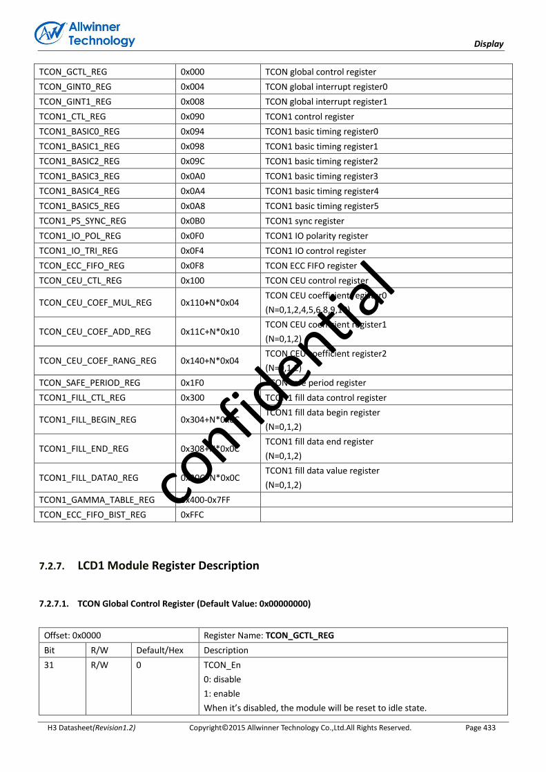
Display
H3 Datasheet(Revision1.2) Copyright© 2015 Allwinner Technology Co.,Ltd.All Rights Reserved. Page 433
TCON_GCTL_REG 0x000 TCON global control register
TCON_GINT0_REG 0x004 TCON global interrupt register0
TCON_GINT1_REG 0x008 TCON global interrupt register1
TCON1_CTL_REG 0x090 TCON1 control register
TCON1_BASIC0_REG 0x094 TCON1 basic timing register0
TCON1_BASIC1_REG 0x098 TCON1 basic timing register1
TCON1_BASIC2_REG 0x09C TCON1 basic timing register2
TCON1_BASIC3_REG 0x0A0 TCON1 basic timing register3
TCON1_BASIC4_REG 0x0A4 TCON1 basic timing register4
TCON1_BASIC5_REG 0x0A8 TCON1 basic timing register5
TCON1_PS_SYNC_REG 0x0B0 TCON1 sync register
TCON1_IO_POL_REG 0x0F0 TCON1 IO polarity register
TCON1_IO_TRI_REG 0x0F4 TCON1 IO control register
TCON_ECC_FIFO_REG 0x0F8 TCON ECC FIFO register
TCON_CEU_CTL_REG 0x100 TCON CEU control register
TCON_CEU_COEF_MUL_REG 0x110+N*0x04 TCON CEU coefficient register0
(N=0,1,2,4,5,6,8,9,10)
TCON_CEU_COEF_ADD_REG 0x11C+N*0x10 TCON CEU coefficient register1
(N=0,1,2)
TCON_CEU_COEF_RANG_REG 0x140+N*0x04 TCON CEU coefficient register2
(N=0,1,2)
TCON_SAFE_PERIOD_REG 0x1F0 TCON safe period register
TCON1_FILL_CTL_REG 0x300 TCON1 fill data control register
TCON1_FILL_BEGIN_REG 0x304+N*0x0C TCON1 fill data begin register
(N=0,1,2)
TCON1_FILL_END_REG 0x308+N*0x0C TCON1 fill data end register
(N=0,1,2)
TCON1_FILL_DATA0_REG 0x30C+N*0x0C TCON1 fill data value register
(N=0,1,2)
TCON1_GAMMA_TABLE_REG 0x400-0x7FF
TCON_ECC_FIFO_BIST_REG 0xFFC
7.2.7. LCD1 Module Register Description
7.2.7.1. TCON Global Control Register (Default Value: 0x00000000)
Offset: 0x0000 Register Name: TCON_GCTL_REG
Bit R/W Default/Hex Description
31 R/W 0 TCON_En
0: disable
1: enable
When it’s disabled, the module will be reset to idle state.
confid
ential

Display
H3 Datasheet(Revision1.2) Copyright© 2015 Allwinner Technology Co.,Ltd.All Rights Reserved. Page 434
30 R/W 0 TCON_Gamma_En
0: disable
1: enable
29:0 / / /
7.2.7.2. TCON Global Interrupt Register0 (Default Value: 0x00000000)
Offset: 0x0004 Register Name: TCON_GINT0_REG
Bit R/W Default/Hex Description
31 / / /
30 R/W 0 TCON1_Vb_Int_En
0: disable
1: enable
29 / / /
28 R/W 0 TCON1_Line_Int_En
0: disable
1: enable
27:15 / / /
14 R/W 0 TCON1_Vb_Int_Flag
Asserted during vertical no-display period every frame.
Write 0 to clear it.
13 / / /
12 R/W 0 TCON1_Line_Int_Flag
trigger when SY1 match the current TCON1 scan line
Write 0 to clear it.
11:0 / 0 /
7.2.7.3. TCON Global Interrupt Register1 (Default Value: 0x00000000)
Offset: 0x0008 Register Name: TCON_GINT1_REG
Bit R/W Default/Hex Description
31:12 / / /
11:0 R/W 0 TCON1_Line_Int_Num
scan line for TCON1 line trigger(including inactive lines)
Setting it for the specified line for trigger 1.
Note: SY1 is writable only when LINE_TRG1 disable.
7.2.7.4. TCON1 Control Register (Default Value: 0x00000000)
Offset: 0x0090 Register Name: TCON1_CTL_REG
Bit R/W Default/Hex Description
confid
ential

Display
H3 Datasheet(Revision1.2) Copyright© 2015 Allwinner Technology Co.,Ltd.All Rights Reserved. Page 435
31 R/W 0 TCON1_En
0: disable
1: enable
30:9 / / /
8:4 R/W 0 Start_Delay
This is for DE1 and DE2
3:2 / / /
1 R/W 0 TCON1_Src_Sel
00: DE 0
01: BLUE data(FIFO2 disable,RGB = 0000FF)
0 / / /
7.2.7.5. TCON1 Basic Timing Register0 (Default Value: 0x00000000)
Offset: 0x0094 Register Name: TCON1_BASIC0_REG
Bit R/W Default/Hex Description
31:28 / / /
27:16 R/W 0 TCON1_XI
source width is X+1
15:12 / / /
11:0 R/W 0 TCON1_YI
source height is Y+1
7.2.7.6. TCON1 Basic Timing Register1 (Default Value: 0x00000000)
Offset: 0x0098 Register Name: TCON1_BASIC1_REG
Bit R/W Default/Hex Description
31:28 / / /
27:16 R/W 0 LS_XO
width is LS_XO+1
15:12 / / /
11:0 R/W 0 LS_YO
width is LS_YO+1
NOTE: this version LS_YO = TCON1_YI
7.2.7.7. TCON1 Basic Timing Register2 (Default Value: 0x00000000)
Offset: 0x009C Register Name: TCON1_BASIC2_REG
Bit R/W Default/Hex Description
31:28 / / /
27:16 R/W 0 TCON1_XO
confid
ential
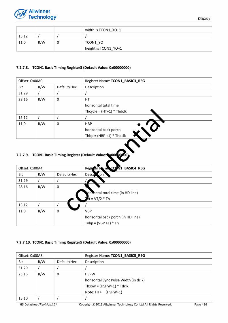
Display
H3 Datasheet(Revision1.2) Copyright© 2015 Allwinner Technology Co.,Ltd.All Rights Reserved. Page 436
width is TCON1_XO+1
15:12 / / /
11:0 R/W 0 TCON1_YO
height is TCON1_YO+1
7.2.7.8. TCON1 Basic Timing Register3 (Default Value: 0x00000000)
Offset: 0x00A0 Register Name: TCON1_BASIC3_REG
Bit R/W Default/Hex Description
31:29 / / /
28:16 R/W 0 HT
horizontal total time
Thcycle = (HT+1) * Thdclk
15:12 / / /
11:0 R/W 0 HBP
horizontal back porch
Thbp = (HBP +1) * Thdclk
7.2.7.9. TCON1 Basic Timing Register (Default Value: 0x00000000)
Offset: 0x00A4 Register Name: TCON1_BASIC4_REG
Bit R/W Default/Hex Description
31:29 / / /
28:16 R/W 0 VT
horizontal total time (in HD line)
Tvt = VT/2 * Th
15:12 / / /
11:0 R/W 0 VBP
horizontal back porch (in HD line)
Tvbp = (VBP +1) * Th
7.2.7.10. TCON1 Basic Timing Register5 (Default Value: 0x00000000)
Offset: 0x00A8 Register Name: TCON1_BASIC5_REG
Bit R/W Default/Hex Description
31:29 / / /
25:16 R/W 0 HSPW
horizontal Sync Pulse Width (in dclk)
Thspw = (HSPW+1) * Tdclk
Note: HT> (HSPW+1)
15:10 / / /
confid
ential

Display
H3 Datasheet(Revision1.2) Copyright© 2015 Allwinner Technology Co.,Ltd.All Rights Reserved. Page 437
9:0 R/W 0 VSPW
vertical Sync Pulse Width (in lines)
Tvspw = (VSPW+1) * Th
Note: VT/2 > (VSPW+1)
7.2.7.11. TCON CEU Control Register (Default Value: 0x00000000)
Offset: 0x0100 Register Name: TCON_CEU_CTL_REG
Bit R/W Default/Hex Description
31 R/W 0 CEU_en
0: bypass
1: enable
30:0 / / /
7.2.7.12. TCON CEU Coefficient Mul Register (Default Value: 0x00000000)
Offset: 0x0110+N*0x04
(N=0,1,2,4,5,6,8,9,10)
Register Name: TCON_CEU_COEF_MUL_REG
Bit R/W Default/Hex Description
31:13 / / /
12:0 R/W 0 CEU_Coef_Mul_Value
signed 13bit value, range of (-16,16)
N=0: Rr
N=1: Rg
N=2: Rb
N=4: Gr
N=5: Gg
N=6: Gb
N=8: Br
N=9: Bg
N=10: Bb
7.2.7.13. TCON CEU Coefficient Add Register (Default Value: 0x00000000)
Offset: 0x011C+N*0x10
(N=0,1,2)
Register Name: TCON_CEU_COEF_ADD_REG
Bit R/W Default/Hex Description
31:19 / / /
18:0 R/W 0 CEU_Coef_Add_Value
signed 19bit value, range of (-16384, 16384)
N=0: Rc
confid
ential
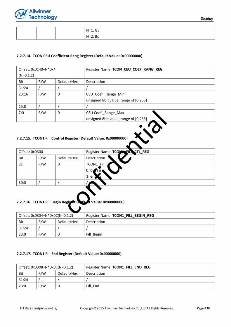
Display
H3 Datasheet(Revision1.2) Copyright© 2015 Allwinner Technology Co.,Ltd.All Rights Reserved. Page 438
N=1: Gc
N=2: Bc
7.2.7.14. TCON CEU Coefficient Rang Register (Default Value: 0x00000000)
Offset: 0x0140+N*0x4
(N=0,1,2)
Register Name: TCON_CEU_COEF_RANG_REG
Bit R/W Default/Hex Description
31:24 / / /
23:16 R/W 0 CEU_Coef _Range_Min
unsigned 8bit value, range of [0,255]
15:8 / / /
7:0 R/W 0 CEU Coef _Range_Max
unsigned 8bit value, range of [0,255]
7.2.7.15. TCON1 Fill Control Register (Default Value: 0x00000000)
Offset: 0x0300 Register Name: TCON1_FILL_CTL_REG
Bit R/W Default/Hex Description
31 R/W 0 TCON1_Fill_En
0: bypass
1: enable
30:0 / / /
7.2.7.16. TCON1 Fill Begin Register (Default Value: 0x00000000)
Offset: 0x0304+N*0x0C(N=0,1,2) Register Name: TCON1_FILL_BEGIN_REG
Bit R/W Default/Hex Description
31:24 / / /
23:0 R/W 0 Fill_Begin
7.2.7.17. TCON1 Fill End Register (Default Value: 0x00000000)
Offset: 0x0308+N*0x0C(N=0,1,2) Register Name: TCON1_FILL_END_REG
Bit R/W Default/Hex Description
31:24 / / /
23:0 R/W 0 Fill_End
confid
ential
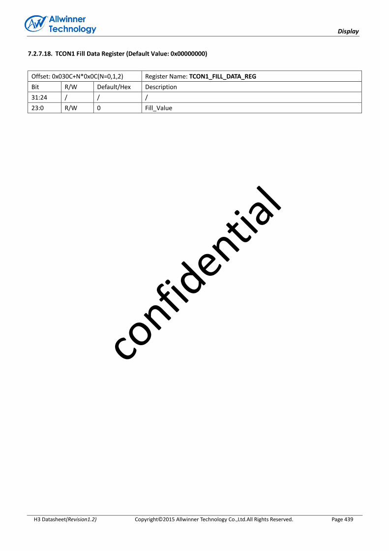
Display
H3 Datasheet(Revision1.2) Copyright© 2015 Allwinner Technology Co.,Ltd.All Rights Reserved. Page 439
7.2.7.18. TCON1 Fill Data Register (Default Value: 0x00000000)
Offset: 0x030C+N*0x0C(N=0,1,2) Register Name: TCON1_FILL_DATA_REG
Bit R/W Default/Hex Description
31:24 / / /
23:0 R/W 0 Fill_Value
confid
ential
Interfaces
H3 Datasheet(Revision1.2) Copyright© 2015 Allwinner Technology Co.,Ltd.All Rights Reserved. Page 440
Chapter 8 Interfaces
This chapter describes the H3 interfaces, including:
TWI
SPI
UART
CIR Receiver
USB
I2S/PCM
OWA
SCR
EMAC
TSC
confid
ential

Interfaces
H3 Datasheet(Revision1.2) Copyright© 2015 Allwinner Technology Co.,Ltd.All Rights Reserved. Page 441
8.1. TWI
8.1.1. Overview
This TWI Controller is designed to be used as an interface between CPU host and the serial TWI bus. It can support all
the standard TWI transfer, including Slave and Master. The communication to the TWI bus is carried out on a byte-wise
basis using interrupt or polled handshaking. This TWI Controller can be operated in standard mode (100K bps) or
fast-mode, supporting data rate up to 400K bps. Multiple Masters and 10-bit addressing Mode are supported for this
specified application. General Call Addressing is also supported in Slave mode.
The TWI Controller includes the following features:
Software-programmable for Slave or Master
Support Repeated START signal
Multi-master systems supported
Allow 10-bit addressing with TWI bus
Performs arbitration and clock synchronization
Own address and General Call address detection
Interrupt on address detection
Support speeds up to 400Kbits/s (‘fast mode’)
Allow operation from a wide range of input clock frequencies
8.1.2. Timing Diagram
Data transferred are always in a unit of 8-bit (byte), followed by an acknowledge bit. The number of bytes that can be
transmitted per transfer is unrestricted. Data is transferred in serial with the MSB first. Between each byte of data
transfer, a receiver device will hold the clock line SCL low to force the transmitter into a wait state while waiting the
response from microprocessor.
Data transfer with acknowledge is obligatory. The clock line is driven by the master all the time, including the
acknowledge-related clock cycle, except for the SCL holding between each bytes. After sending each byte, the
transmitter releases the SDA line to allow the receiver to pull down the SDA line and send an acknowledge signal (or
leave it high to send a "not acknowledge") to the transmitter.
When a slave receiver doesn't acknowledge the slave address (unable to receive because of no resource available), the
data line must be left high by the slave so that the master can then generate a STOP condition to abort the transfer.
Slave receiver can also indicate not to want to send more data during a transfer by leave the acknowledge signal high.
And the master should generate the STOP condition to abort the transfer.
Below diagram provides an illustration the relation of SDA signal line and SCL signal line on the TWI serial bus.
confid
ential

Interfaces
H3 Datasheet(Revision1.2) Copyright© 2015 Allwinner Technology Co.,Ltd.All Rights Reserved. Page 442
IIC2IIC5IIC5IIC4IIC4IIC3IIC1
SDA
SCL
Figure 8-1. TWI Timing Diagram
8.1.3. TWI Controller Special Requirement
8.1.3.1. TWI Pin List
Port Name Width Direction Description
TWI_SCL 1 IN/OUT TWI Clock line
TWI_SDA 1 IN/OUT TWI Serial Data line
8.1.3.2. TWI Controller Operation
There are four operation modes on the TWI bus which dictates the communications method. They are Master Transmit,
Master Receive, Slave Transmit and Slave Receive. In general, CPU host controls TWI by writing commands and data to
its registers. The TWI interrupts the CPU host for the attention each time a byte transfer is done or a START/STOP
conditions is detected. The CPU host can also poll the status register for current status if the interrupt mechanism is not
disabled by the CPU host.
When the CPU host wants to start a bus transfer, it initiates a bus START to enter the master mode by setting IM_STA bit
in the 2WIRE_CNTR register to high (before it must be low). The TWI will assert INT line and INT_FLAG to indicate a
completion for the START condition and each consequent byte transfer. At each interrupt, the micro-processor needs to
check the 2WIRE_STAT register for current status. A transfer has to be concluded with STOP condition by setting M_STP
bit high.
In Slave Mode, the TWI also constantly samples the bus and look for its own slave address during addressing cycles.
Once a match is found, it is addressed and interrupt the CPU host with the corresponding status. Upon request, the CPU
host should read the status, read/write 2WIRE_DATA data register, and set the 2WIRE_CNTR control register. After each
byte transfer, a slave device always halt the operation of remote master by holding the next low pulse on SCL line until
the microprocessor responds to the status of previous byte transfer or START condition.
8.1.4. TWI Controller Register List
Module Name Base Address
R_TWI 0x01F02400
confid
ential

Interfaces
H3 Datasheet(Revision1.2) Copyright© 2015 Allwinner Technology Co.,Ltd.All Rights Reserved. Page 443
TWI0 0x01C2AC00
TWI1 0x01C2B000
TWI2 0x01C2B400
Register Name Offset Description
TWI_ADDR 0x0000 TWI Slave address
TWI_XADDR 0x0004 TWI Extended slave address
TWI_DATA 0x0008 TWI Data byte
TWI_CNTR 0x000C TWI Control register
TWI_STAT 0x0010 TWI Status register
TWI_CCR 0x0014 TWI Clock control register
TWI_SRST 0x0018 TWI Software reset
TWI_EFR 0x001C TWI Enhance Feature register
TWI_LCR 0x0020 TWI Line Control register
8.1.5. TWI Controller Register Description
8.1.5.1. TWI Slave Address Register(Default Value: 0x00000000)
Offset: 0x00 Register Name: TWI_ADDR
Bit R/W Default/Hex Description
31:8 / / /
7:1 R/W 0
SLA
Slave address
7-bit addressing
SLA6, SLA5, SLA4, SLA3, SLA2, SLA1, SLA0
10-bit addressing
1, 1, 1, 1, 0, SLAX[9:8]
0 R/W 0
GCE
General call address enable
0: Disable
1: Enable
Notes:
For 7-bit addressing:
SLA6 – SLA0 is the 7-bit address of the TWI when in slave mode. When the TWI receives this address after a START
condition, it will generate an interrupt and enter slave mode. (SLA6 corresponds to the first bit received from the TWI
bus.) If GCE is set to ‘1’, the TWI will also recognize the general call address (00h).
For 10-bit addressing:
When the address received starts with 11110b, the TWI recognizes this as the first part of a 10-bit address and if the
next two bits match ADDR[2:1] (i.e. SLAX9 and SLAX8 of the device’s extended address), it sends an ACK. (The device
confid
ential

Interfaces
H3 Datasheet(Revision1.2) Copyright© 2015 Allwinner Technology Co.,Ltd.All Rights Reserved. Page 444
does not generate an interrupt at this point.) If the next byte of the address matches the XADDR register (SLAX7 –
SLAX0), the TWI generates an interrupt and goes into slave mode.
8.1.5.2. TWI Extend Address Register(Default Value: 0x00000000)
Offset: 0x04 Register Name: TWI_XADDR
Bit R/W Default/Hex Description
31:8 / / /
7:0 R/W 0
SLAX
Extend Slave Address
SLAX[7:0]
8.1.5.3. TWI Data Register(Default Value: 0x00000000)
Offset: 0x08 Register Name: TWI_DATA
Bit R/W Default/Hex Description
31:8 / / /
7:0 R/W 0 TWI_DATA
Data byte for transmitting or received
8.1.5.4. TWI Control Register(Default Value: 0x00000000)
Offset: 0x0C Register Name: TWI_ CNTR
Bit R/W Default/Hex Description
31:8 / / /
7 R/W 0
INT_EN
Interrupt Enable
1’b0: The interrupt line always low
1’b1: The interrupt line will go high when INT_FLAG is set.
6 R/W 0
BUS_EN
TWI Bus Enable
1’b0: The TWI bus inputs ISDA/ISCL are ignored and the TWI Controller will
not respond to any address on the bus
1’b1: The TWI will respond to calls to its slave address – and to the general
call address if the GCE bit in the ADDR register is set.
Notes: In master operation mode, this bit should be set to ‘1’
5 R/W 0
M_STA
Master Mode Start
When M_STA is set to ‘1’, TWI Controller enters master mode and will
transmit a START condition on the bus when the bus is free. If the M_STA bit
confid
ential
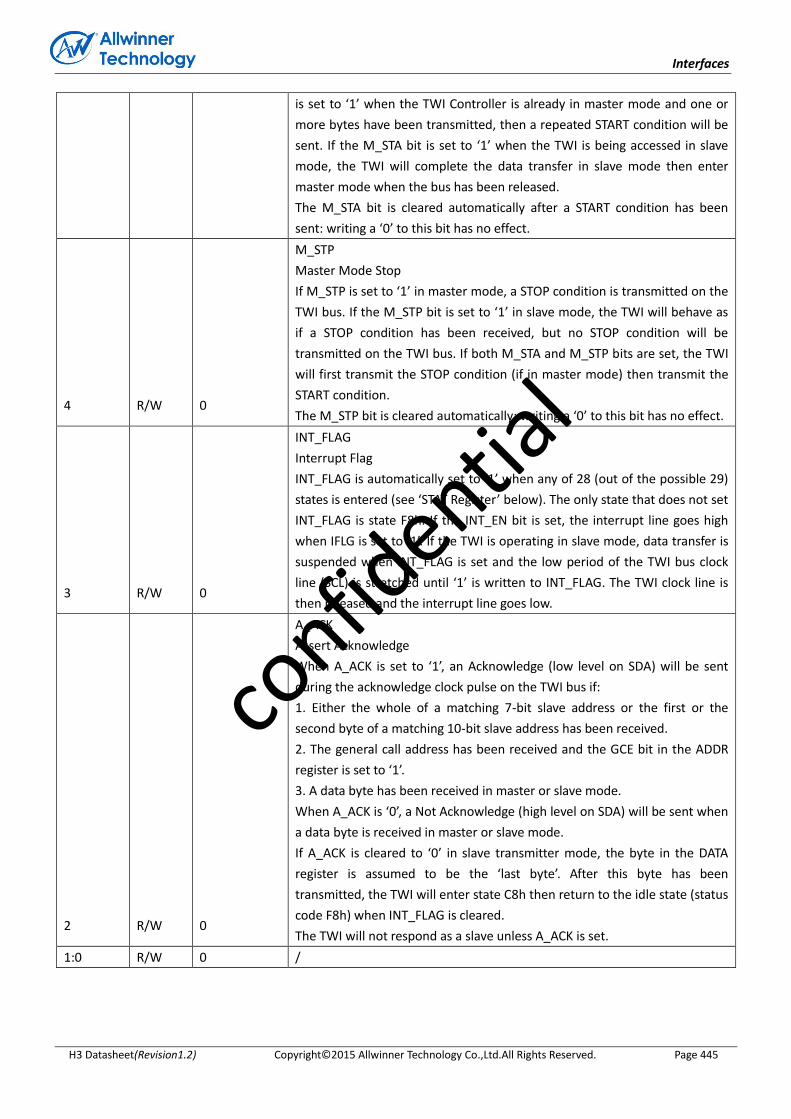
Interfaces
H3 Datasheet(Revision1.2) Copyright© 2015 Allwinner Technology Co.,Ltd.All Rights Reserved. Page 445
is set to ‘1’ when the TWI Controller is already in master mode and one or
more bytes have been transmitted, then a repeated START condition will be
sent. If the M_STA bit is set to ‘1’ when the TWI is being accessed in slave
mode, the TWI will complete the data transfer in slave mode then enter
master mode when the bus has been released.
The M_STA bit is cleared automatically after a START condition has been
sent: writing a ‘0’ to this bit has no effect.
4 R/W 0
M_STP
Master Mode Stop
If M_STP is set to ‘1’ in master mode, a STOP condition is transmitted on the
TWI bus. If the M_STP bit is set to ‘1’ in slave mode, the TWI will behave as
if a STOP condition has been received, but no STOP condition will be
transmitted on the TWI bus. If both M_STA and M_STP bits are set, the TWI
will first transmit the STOP condition (if in master mode) then transmit the
START condition.
The M_STP bit is cleared automatically: writing a ‘0’ to this bit has no effect.
3 R/W 0
INT_FLAG
Interrupt Flag
INT_FLAG is automatically set to ‘1’ when any of 28 (out of the possible 29)
states is entered (see ‘STAT Register’ below). The only state that does not set
INT_FLAG is state F8h. If the INT_EN bit is set, the interrupt line goes high
when IFLG is set to ‘1’. If the TWI is operating in slave mode, data transfer is
suspended when INT_FLAG is set and the low period of the TWI bus clock
line (SCL) is stretched until ‘1’ is written to INT_FLAG. The TWI clock line is
then released and the interrupt line goes low.
2 R/W 0
A_ACK
Assert Acknowledge
When A_ACK is set to ‘1’, an Acknowledge (low level on SDA) will be sent
during the acknowledge clock pulse on the TWI bus if:
1. Either the whole of a matching 7-bit slave address or the first or the
second byte of a matching 10-bit slave address has been received.
2. The general call address has been received and the GCE bit in the ADDR
register is set to ‘1’.
3. A data byte has been received in master or slave mode.
When A_ACK is ‘0’, a Not Acknowledge (high level on SDA) will be sent when
a data byte is received in master or slave mode.
If A_ACK is cleared to ‘0’ in slave transmitter mode, the byte in the DATA
register is assumed to be the ‘last byte’. After this byte has been
transmitted, the TWI will enter state C8h then return to the idle state (status
code F8h) when INT_FLAG is cleared.
The TWI will not respond as a slave unless A_ACK is set.
1:0 R/W 0 /
confid
ential

Interfaces
H3 Datasheet(Revision1.2) Copyright© 2015 Allwinner Technology Co.,Ltd.All Rights Reserved. Page 446
8.1.5.5. TWI Status Register(Default Value: 0x000000F8)
Offset: 0x10 Register Name: TWI_STAT
Bit R/W Default/Hex Description
31:8 / / /
7:0 R 0xF8
STA
Status Information Byte
Code Status
0x00: Bus error
0x08: START condition transmitted
0x10: Repeated START condition transmitted
0x18: Address + Write bit transmitted, ACK received
0x20: Address + Write bit transmitted, ACK not received
0x28: Data byte transmitted in master mode, ACK received
0x30: Data byte transmitted in master mode, ACK not received
0x38: Arbitration lost in address or data byte
0x40: Address + Read bit transmitted, ACK received
0x48: Address + Read bit transmitted, ACK not received
0x50: Data byte received in master mode, ACK transmitted
0x58: Data byte received in master mode, not ACK transmitted
0x60: Slave address + Write bit received, ACK transmitted
0x68: Arbitration lost in address as master, slave address + Write bit
received, ACK transmitted
0x70: General Call address received, ACK transmitted
0x78: Arbitration lost in address as master, General Call address received,
ACK transmitted
0x80: Data byte received after slave address received, ACK transmitted
0x88: Data byte received after slave address received, not ACK transmitted
0x90: Data byte received after General Call received, ACK transmitted
0x98: Data byte received after General Call received, not ACK transmitted
0xA0: STOP or repeated START condition received in slave mode
0xA8: Slave address + Read bit received, ACK transmitted
0xB0: Arbitration lost in address as master, slave address + Read bit received,
ACK transmitted
0xB8: Data byte transmitted in slave mode, ACK received
0xC0: Data byte transmitted in slave mode, ACK not received
0xC8: Last byte transmitted in slave mode, ACK received
0xD0: Second Address byte + Write bit transmitted, ACK received
0xD8: Second Address byte + Write bit transmitted, ACK not received
0xF8: No relevant status information, INT_FLAG=0
Others: Reserved
confid
ential

Interfaces
H3 Datasheet(Revision1.2) Copyright© 2015 Allwinner Technology Co.,Ltd.All Rights Reserved. Page 447
8.1.5.6. TWI Clock Register(Default Value: 0x00000000)
Offset: 0x14 Register Name: TWI_CCR
Bit R/W Default/Hex Description
31:7 / / /
6:3 R/W 0 CLK_M
2:0 R/W 0
CLK_N
The TWI bus is sampled by the TWI at the frequency defined by F0:
Fsamp = F 0 = Fin / 2^CLK_N
The TWI OSCL output frequency, in master mode, is F1 / 10:
F1 = F0 / (CLK_M + 1)
Foscl = F1 / 10 = Fin / (2^CLK_N * (CLK_M + 1)*10)
For Example:
Fin = 48Mhz (APB clock input)
For 400kHz full speed 2Wire, CLK_N = 2, CLK_M=2
F0 = 48M/2^2=12Mhz, F1= F0/(10*(2+1)) = 0.4Mhz
For 100Khz standard speed 2Wire, CLK_N=2, CLK_M=11
F0=48M/2^2=12Mhz, F1=F0/(10*(11+1)) = 0.1Mhz
8.1.5.7. TWI Soft Reset Register(Default Value: 0x00000000)
Offset: 0x18 Register Name: TWI_SRST
Bit R/W Default/Hex Description
31:1 / / /
0 R/W 0
SOFT_RST
Soft Reset
Write ‘1’ to this bit to reset the TWI and clear to ‘0’ when completing Soft
Reset operation.
8.1.5.8. TWI Enhance Feature Register(Default Value: 0x00000000)
Offset: 0x1C Register Name: TWI_EFR
Bit R/W Default/Hex Description
31:2 / / /
0:1 R/W 0
DBN
Data Byte number follow Read Command Control
0— No Data Byte to be written after read command
1— Only 1 byte data to be written after read command
2— 2 bytes data can be written after read command
3— 3 bytes data can be written after read command
confid
ential

Interfaces
H3 Datasheet(Revision1.2) Copyright© 2015 Allwinner Technology Co.,Ltd.All Rights Reserved. Page 448
8.1.5.9. TWI Line Control Register(Default Value: 0x0000_003A)
Offset: 0x20 Register Name: TWI_LCR
Bit R/W Default/Hex Description
31:6 / / /
5 R 1
SCL_STATE
Current state of TWI_SCL
0 – low
1 - high
4 R 1
SDA_STATE
Current state of TWI_SDA
0 – low
1 - high
3 R/W 1
SCL_CTL
TWI_SCL line state control bit
When line control mode is enabled (bit[2] set), value of this bit decide the
output level of TWI_SCL
0 – output low level
1 – output high level
2 R/W 0
SCL_CTL_EN
TWI_SCL line state control enable
When this bit is set, the state of TWI_SCL is control by the value of bit[3].
0-disable TWI_SCL line control mode
1-enable TWI_SCL line control mode
1 R/W 1
SDA_CTL
TWI_SDA line state control bit
When line control mode is enabled (bit[0] set), value of this bit decide the
output level of TWI_SDA
0 – output low level
1 – output high level
0 R/W 0
SDA_CTL_EN
TWI_SDA line state control enable
When this bit is set, the state of TWI_SDA is control by the value of bit[1].
0-disable TWI_SDA line control mode
1-enable TWI_SDA line control mode
8.1.5.10. TWI DVFS Register(Default Value: 0x00000000)
Offset: 0x24 Register Name: TWI_DVFSCR
Bit R/W Default/Hex Description
31:3 / / /
2 R/W 0 MS_PRIORITY
CPU and DVFS BUSY set priority select
confid
ential

Interfaces
H3 Datasheet(Revision1.2) Copyright© 2015 Allwinner Technology Co.,Ltd.All Rights Reserved. Page 449
0: CPU has higher priority
1: DVFS has higher priority
1 R/W 0 CPU_BUSY_SET
CPU Busy set
0 R/W 0 DVFC_BUSY_SET
DVFS Busy set
Notes:This register is only implemented in TWI0.
confid
ential

Interfaces
H3 Datasheet(Revision1.2) Copyright© 2015 Allwinner Technology Co.,Ltd.All Rights Reserved. Page 450
8.2. SPI
8.2.1. Overview
The SPI is the Serial Peripheral Interface which allows rapid data communication with fewer software interrupts. It can
interface with up to four slave external devices or one single external master.The SPI module contains one 64x8
receiver buffer (RXFIFO) and one64x8 transmit buffer (TXFIFO). It can work at two modes: Master mode and Slave
mode.
The SPI includes the following features:
Full-duplex synchronous serial interface
Master/Slave configurable
Programmable clock granularity
Four chip selects to support multiple peripherals
8-bit wide by 64-entry FIFO for both transmit and receive date
Polarity and phase of the Chip Select (SPI_SS) and SPI Clock (SPI_SCLK) are configurable
Interrupt or DMA supported
Support single and dual read mode
8.2.2. SPI Timing Diagram
The serial peripheral interface master uses the SPI_SCLK signal to transfer data in and out of the shift register. Data is
clocked using any one of four programmable clock phase and polarity combinations.
During Phase 0, Polarity 0 and Phase 1, Polarity 1 operations, output data changes on the falling clock edge and input
data is shifted in on the rising edge.
During Phase 1, Polarity 0 and Phase 0, Polarity 1 operations, output data changes on the rising edges of the clock and
is shifted in on falling edges.
The POL defines the signal polarity when SPI_SCLK is in idle state. The SPI_SCLK is high level when POL is ‘1’ and it is low
level when POL is ‘0’. The PHA decides whether the leading edge of SPI_SCLK is used for setup or sample data. The
leading edge is used for setup data when PHA is ‘1’ and for sample data when PHA is ‘0’. The four kind of modes are
listed below:
SPI Mode POL PHA Leading Edge Trailing Edge
0 0 0 Rising, Sample Falling, Setup
1 0 1 Rising, Setup Falling, Sample
2 1 0 Falling, Sample Rising, Setup
3 1 1 Failing, Setup Rising, Sample
confid
ential

Interfaces
H3 Datasheet(Revision1.2) Copyright© 2015 Allwinner Technology Co.,Ltd.All Rights Reserved. Page 451
Phase 0
SPI_SCLK (Mode 0)
SPI_SCLK (Mode 2)
SPI_MOSI
SPI_MISO
SPI_SS
Sample MOSI/ MISO pin
Figure 8-2. SPI Phase 0 Timing Diagram
Phase 1
SPI_SCLK (Mode 1)
SPI_SCLK (Mode 3)
SPI_MOSI
SPI_MISO
SPI_SS
Sample MOSI/ MISO pin
Figure 8-3. SPI Phase 1 Timing Diagram
8.2.3. SPI Pin List
The direction of SPI pin is different in two work modes: Master Mode and Slave Mode.
Port Name Width Direction(M) Direction(S) Description
SPI_SCLK 1 OUT IN SPI Clock
SPI_MOSI 1 OUT IN SPI Master Output Slave Input Data Signal
SPI_MISO 1 IN OUT SPI Master Input Slave Output Data Signal
SPI_SS[3:0] 4 OUT IN SPI Chip Select Signal
8.2.4. SPI Register List
Module Name Base Address
confid
ential
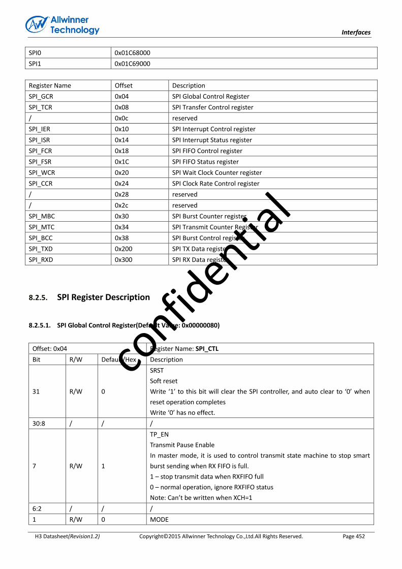
Interfaces
H3 Datasheet(Revision1.2) Copyright© 2015 Allwinner Technology Co.,Ltd.All Rights Reserved. Page 452
SPI0 0x01C68000
SPI1 0x01C69000
Register Name Offset Description
SPI_GCR 0x04 SPI Global Control Register
SPI_TCR 0x08 SPI Transfer Control register
/ 0x0c reserved
SPI_IER 0x10 SPI Interrupt Control register
SPI_ISR 0x14 SPI Interrupt Status register
SPI_FCR 0x18 SPI FIFO Control register
SPI_FSR 0x1C SPI FIFO Status register
SPI_WCR 0x20 SPI Wait Clock Counter register
SPI_CCR 0x24 SPI Clock Rate Control register
/ 0x28 reserved
/ 0x2c reserved
SPI_MBC 0x30 SPI Burst Counter register
SPI_MTC 0x34 SPI Transmit Counter Register
SPI_BCC 0x38 SPI Burst Control register
SPI_TXD 0x200 SPI TX Data register
SPI_RXD 0x300 SPI RX Data register
8.2.5. SPI Register Description
8.2.5.1. SPI Global Control Register(Default Value: 0x00000080)
Offset: 0x04 Register Name: SPI_CTL
Bit R/W Default/Hex Description
31 R/W 0
SRST
Soft reset
Write ‘1’ to this bit will clear the SPI controller, and auto clear to ‘0’ when
reset operation completes
Write ‘0’ has no effect.
30:8 / / /
7 R/W 1
TP_EN
Transmit Pause Enable
In master mode, it is used to control transmit state machine to stop smart
burst sending when RX FIFO is full.
1 – stop transmit data when RXFIFO full
0 – normal operation, ignore RXFIFO status
Note: Can’t be written when XCH=1
6:2 / / /
1 R/W 0 MODE
confid
ential
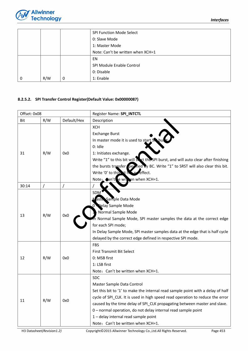
Interfaces
H3 Datasheet(Revision1.2) Copyright© 2015 Allwinner Technology Co.,Ltd.All Rights Reserved. Page 453
SPI Function Mode Select
0: Slave Mode
1: Master Mode
Note: Can’t be written when XCH=1
0 R/W 0
EN
SPI Module Enable Control
0: Disable
1: Enable
8.2.5.2. SPI Transfer Control Register(Default Value: 0x00000087)
Offset: 0x08 Register Name: SPI_INTCTL
Bit R/W Default/Hex Description
31 R/W 0x0
XCH
Exchange Burst
In master mode it is used to start SPI burst
0: Idle
1: Initiates exchange.
Write “1” to this bit will start the SPI burst, and will auto clear after finishing
the bursts transfer specified by BC. Write “1” to SRST will also clear this bit.
Write ‘0’ to this bit has no effect.
Note:Can’t be written when XCH=1.
30:14 / / /
13 R/W 0x0
SDM
Master Sample Data Mode
0 - Delay Sample Mode
1 - Normal Sample Mode
In Normal Sample Mode, SPI master samples the data at the correct edge
for each SPI mode;
In Delay Sample Mode, SPI master samples data at the edge that is half cycle
delayed by the correct edge defined in respective SPI mode.
12 R/W 0x0
FBS
First Transmit Bit Select
0: MSB first
1: LSB first
Note:Can’t be written when XCH=1.
11 R/W 0x0
SDC
Master Sample Data Control
Set this bit to ‘1’ to make the internal read sample point with a delay of half
cycle of SPI_CLK. It is used in high speed read operation to reduce the error
caused by the time delay of SPI_CLK propagating between master and slave.
0 – normal operation, do not delay internal read sample point
1 – delay internal read sample point
Note:Can’t be written when XCH=1.
confid
ential

Interfaces
H3 Datasheet(Revision1.2) Copyright© 2015 Allwinner Technology Co.,Ltd.All Rights Reserved. Page 454
10 R/W 0x0
RPSM
Rapids mode select
Select Rapids mode for high speed write.
0: normal write mode
1: rapids write mode
Note:Can’t be written when XCH=1.
9 R/W 0x0
DDB
Dummy Burst Type
0: The bit value of dummy SPI burst is zero
1: The bit value of dummy SPI burst is one
Note:Can’t be written when XCH=1.
8 R/W 0x0
DHB
Discard Hash Burst
In master mode it controls whether discarding unused SPI bursts
0: Receiving all SPI bursts in BC period
1: Discard unused SPI bursts, only fetching the SPI bursts during dummy
burst period. The bursts number is specified by TC.
Note:Can’t be written when XCH=1.
7 R/W 0x1
SS_LEVEL
When control SS signal manually (SPI_CTRL_REG.SS_CTRL==1), set this bit to
‘1’ or ‘0’ to control the level of SS signal.
0: set SS to low
1: set SS to high
Note:Can’t be written when XCH=1.
6 R/W 0x0
SS_OWNER
SS Output Owner Select
Usually, controller sends SS signal automatically with data together. When
this bit is set to 1, software must manually write SPI_CTL_REG.SS_LEVEL to 1
or 0 to control the level of SS signal.
0: SPI controller
1: Software
Note:Can’t be written when XCH=1.
5:4 R/W 0x0
SS_SEL
SPI Chip Select
Select one of four external SPI Master/Slave Devices
00: SPI_SS0 will be asserted
01: SPI_SS1 will be asserted
10: SPI_SS2 will be asserted
11: SPI_SS3 will be asserted
Note:Can’t be written when XCH=1.
3 R/W 0x0
SSCTL
In master mode, this bit selects the output wave form for the SPI_SSx signal.
Only valid when SS_OWNER = 0.
0: SPI_SSx remains asserted between SPI bursts
1: Negate SPI_SSx between SPI bursts
confid
ential
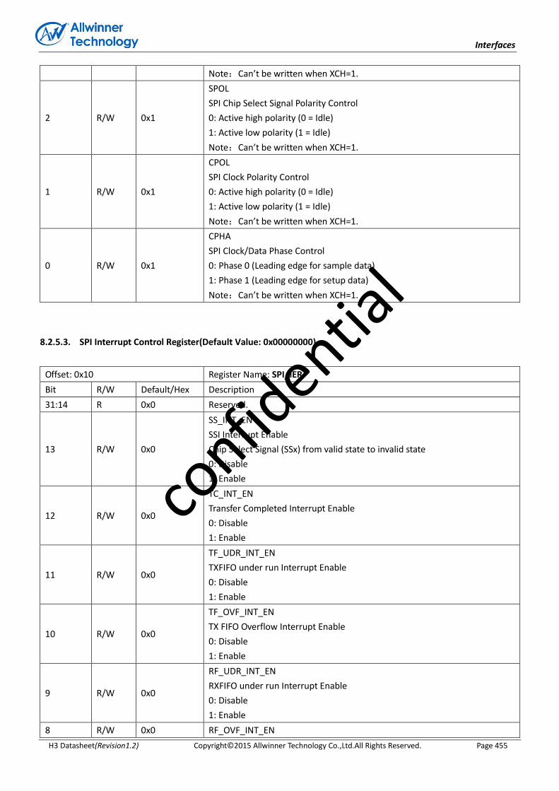
Interfaces
H3 Datasheet(Revision1.2) Copyright© 2015 Allwinner Technology Co.,Ltd.All Rights Reserved. Page 455
Note:Can’t be written when XCH=1.
2 R/W 0x1
SPOL
SPI Chip Select Signal Polarity Control
0: Active high polarity (0 = Idle)
1: Active low polarity (1 = Idle)
Note:Can’t be written when XCH=1.
1 R/W 0x1
CPOL
SPI Clock Polarity Control
0: Active high polarity (0 = Idle)
1: Active low polarity (1 = Idle)
Note:Can’t be written when XCH=1.
0 R/W 0x1
CPHA
SPI Clock/Data Phase Control
0: Phase 0 (Leading edge for sample data)
1: Phase 1 (Leading edge for setup data)
Note:Can’t be written when XCH=1.
8.2.5.3. SPI Interrupt Control Register(Default Value: 0x00000000)
Offset: 0x10 Register Name: SPI_IER
Bit R/W Default/Hex Description
31:14 R 0x0 Reserved.
13 R/W 0x0
SS_INT_EN
SSI Interrupt Enable
Chip Select Signal (SSx) from valid state to invalid state
0: Disable
1: Enable
12 R/W 0x0
TC_INT_EN
Transfer Completed Interrupt Enable
0: Disable
1: Enable
11 R/W 0x0
TF_UDR_INT_EN
TXFIFO under run Interrupt Enable
0: Disable
1: Enable
10 R/W 0x0
TF_OVF_INT_EN
TX FIFO Overflow Interrupt Enable
0: Disable
1: Enable
9 R/W 0x0
RF_UDR_INT_EN
RXFIFO under run Interrupt Enable
0: Disable
1: Enable
8 R/W 0x0 RF_OVF_INT_EN
confid
ential
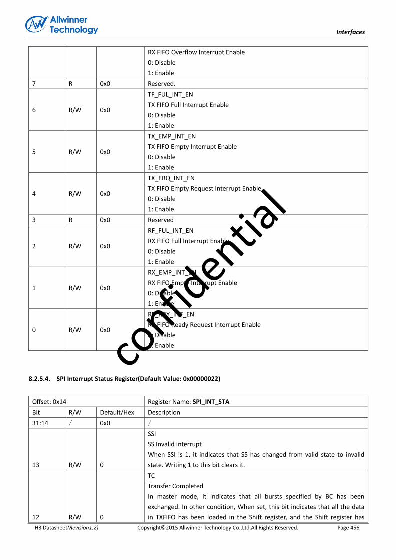
Interfaces
H3 Datasheet(Revision1.2) Copyright© 2015 Allwinner Technology Co.,Ltd.All Rights Reserved. Page 456
RX FIFO Overflow Interrupt Enable
0: Disable
1: Enable
7 R 0x0 Reserved.
6 R/W 0x0
TF_FUL_INT_EN
TX FIFO Full Interrupt Enable
0: Disable
1: Enable
5 R/W 0x0
TX_EMP_INT_EN
TX FIFO Empty Interrupt Enable
0: Disable
1: Enable
4 R/W 0x0
TX_ERQ_INT_EN
TX FIFO Empty Request Interrupt Enable
0: Disable
1: Enable
3 R 0x0 Reserved
2 R/W 0x0
RF_FUL_INT_EN
RX FIFO Full Interrupt Enable
0: Disable
1: Enable
1 R/W 0x0
RX_EMP_INT_EN
RX FIFO Empty Interrupt Enable
0: Disable
1: Enable
0 R/W 0x0
RF_RDY_INT_EN
RX FIFO Ready Request Interrupt Enable
0: Disable
1: Enable
8.2.5.4. SPI Interrupt Status Register(Default Value: 0x00000022)
Offset: 0x14 Register Name: SPI_INT_STA
Bit R/W Default/Hex Description
31:14 / 0x0 /
13 R/W 0
SSI
SS Invalid Interrupt
When SSI is 1, it indicates that SS has changed from valid state to invalid
state. Writing 1 to this bit clears it.
12 R/W 0
TC
Transfer Completed
In master mode, it indicates that all bursts specified by BC has been
exchanged. In other condition, When set, this bit indicates that all the data
in TXFIFO has been loaded in the Shift register, and the Shift register has
confid
ential

Interfaces
H3 Datasheet(Revision1.2) Copyright© 2015 Allwinner Technology Co.,Ltd.All Rights Reserved. Page 457
shifted out all the bits. Writing 1 to this bit clears it.
0: Busy
1: Transfer Completed
11 R/W 0
TF_UDF
TXFIFO Underrun
This bit is set when if the TXFIFO is underrun. Writing 1 to this bit clears it.
0: TXFIFO is not underrun
1: TXFIFO is underrun
10 R/W 0
TF_OVF
TXFIFO Overflow
This bit is set when if the TXFIFO is overflow. Writing 1 to this bit clears it.
0: TXFIFO is not overflow
1: TXFIFO is overflowed
9 R/W 0
RX_UDF
RXFIFO Underrun
When set, this bit indicates that RXFIFO has underrun. Writing 1 to this bit
clears it.
8 R/W 0
RX_OVF
RXFIFO Overflow
When set, this bit indicates that RXFIFO has overflowed. Writing 1 to this bit
clears it.
0: RXFIFO is available.
1: RXFIFO has overflowed.
7 / / /
6 R/W 0
TX_FULL
TXFIFO Full
This bit is set when if the TXFIFO is full . Writing 1 to this bit clears it.
0: TXFIFO is not Full
1: TXFIFO is Full
5 R/W 1
TX_EMP
TXFIFO Empty
This bit is set if the TXFIFO is empty. Writing 1 to this bit clears it.
0: TXFIFO contains one or more words.
1: TXFIFO is empty
4 R/W 0
TX_READY
TXFIFO Ready
0: TX_WL > TX_TRIG_LEVEL
1: TX_WL <= TX_TRIG_LEVEL
This bit is set any time if TX_WL <= TX_TRIG_LEVEL. Writing “1” to this bit
clears it. Where TX_WL is the water level of RXFIFO
3 / / reserved
2 R/W 0
RX_FULL
RXFIFO Full
This bit is set when the RXFIFO is full . Writing 1 to this bit clears it.
0: Not Full
confid
ential

Interfaces
H3 Datasheet(Revision1.2) Copyright© 2015 Allwinner Technology Co.,Ltd.All Rights Reserved. Page 458
1: Full
1 R/W 1
RX_EMP
RXFIFO Empty
This bit is set when the RXFIFO is empty . Writing 1 to this bit clears it.
0: Not empty
1: empty
0 R/W 0
RX_RDY
RXFIFO Ready
0: RX_WL < RX_TRIG_LEVEL
1: RX_WL >= RX_TRIG_LEVEL
This bit is set any time if RX_WL >= RX_TRIG_LEVEL. Writing “1” to this bit
clears it. Where RX_WL is the water level of RXFIFO.
8.2.5.5. SPI FIFO Control Register(Default Value: 0x00400001)
Offset: 0x18 Register Name: SPI_ FCR
Bit R/W Default/Hex Description
31 R/W 0
TX_FIFO_RST
TX FIFO Reset
Write ‘1’ to this bit will reset the control portion of the TX FIFO and auto
clear to ‘0’ when completing reset operation, write to ‘0’ has no effect.
30 R/W 0
TF_TEST_ENB
TX Test Mode Enable
0: disable
1: enable
Note: In normal mode, TX FIFO can only be read by SPI controller, write ‘1’
to this bit will switch TX FIFO read and write function to AHB bus. This bit is
used to test the TX FIFO, don’t set in normal operation and don’t set
RF_TEST and TF_TEST at the same time.
29:26 / / /
25 / / /
24 R/W 0x0
TF_ DRQ_EN
TX FIFO DMA Request Enable
0: Disable
1: Enable
23:16 R/W 0x40 TX_TRIG_LEVEL
TX FIFO Empty Request Trigger Level
15 R/W 0x0
RF_RST
RXFIFO Reset
Write ‘1’ to this bit will reset the control portion of the receiver FIFO, and
auto clear to ‘0’ when completing reset operation, write ‘0’ to this bit has no
effect.
14 R/W 0x0 RF_TEST
confid
ential
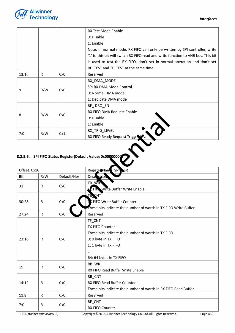
Interfaces
H3 Datasheet(Revision1.2) Copyright© 2015 Allwinner Technology Co.,Ltd.All Rights Reserved. Page 459
RX Test Mode Enable
0: Disable
1: Enable
Note: In normal mode, RX FIFO can only be written by SPI controller, write
‘1’ to this bit will switch RX FIFO read and write function to AHB bus. This bit
is used to test the RX FIFO, don’t set in normal operation and don’t set
RF_TEST and TF_TEST at the same time.
13:10 R 0x0 Reserved
9 R/W 0x0
RX_DMA_MODE
SPI RX DMA Mode Control
0: Normal DMA mode
1: Dedicate DMA mode
8 R/W 0x0
RF_ DRQ_EN
RX FIFO DMA Request Enable
0: Disable
1: Enable
7:0 R/W 0x1 RX_TRIG_LEVEL
RX FIFO Ready Request Trigger Level
8.2.5.6. SPI FIFO Status Register(Default Value: 0x00000000)
Offset: 0x1C Register Name: SPI_FSR
Bit R/W Default/Hex Description
31 R 0x0 TB_WR
TX FIFO Write Buffer Write Enable
30:28 R 0x0
TB_CNT
TX FIFO Write Buffer Counter
These bits indicate the number of words in TX FIFO Write Buffer
27:24 R 0x0 Reserved
23:16 R 0x0
TF_CNT
TX FIFO Counter
These bits indicate the number of words in TX FIFO
0: 0 byte in TX FIFO
1: 1 byte in TX FIFO
…
64: 64 bytes in TX FIFO
15 R 0x0 RB_WR
RX FIFO Read Buffer Write Enable
14:12 R 0x0
RB_CNT
RX FIFO Read Buffer Counter
These bits indicate the number of words in RX FIFO Read Buffer
11:8 R 0x0 Reserved
7:0 R 0x0 RF_CNT
RX FIFO Counter
confid
ential
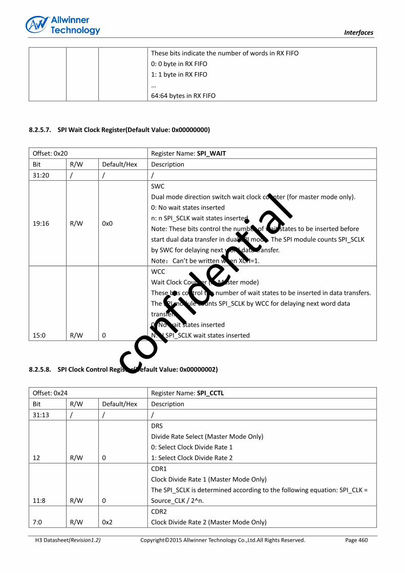
Interfaces
H3 Datasheet(Revision1.2) Copyright© 2015 Allwinner Technology Co.,Ltd.All Rights Reserved. Page 460
These bits indicate the number of words in RX FIFO
0: 0 byte in RX FIFO
1: 1 byte in RX FIFO
…
64:64 bytes in RX FIFO
8.2.5.7. SPI Wait Clock Register(Default Value: 0x00000000)
Offset: 0x20 Register Name: SPI_WAIT
Bit R/W Default/Hex Description
31:20 / / /
19:16 R/W 0x0
SWC
Dual mode direction switch wait clock counter (for master mode only).
0: No wait states inserted
n: n SPI_SCLK wait states inserted
Note: These bits control the number of wait states to be inserted before
start dual data transfer in dual SPI mode. The SPI module counts SPI_SCLK
by SWC for delaying next word data transfer.
Note:Can’t be written when XCH=1.
15:0 R/W 0
WCC
Wait Clock Counter (In Master mode)
These bits control the number of wait states to be inserted in data transfers.
The SPI module counts SPI_SCLK by WCC for delaying next word data
transfer.
0: No wait states inserted
N: N SPI_SCLK wait states inserted
8.2.5.8. SPI Clock Control Register(Default Value: 0x00000002)
Offset: 0x24 Register Name: SPI_CCTL
Bit R/W Default/Hex Description
31:13 / / /
12 R/W 0
DRS
Divide Rate Select (Master Mode Only)
0: Select Clock Divide Rate 1
1: Select Clock Divide Rate 2
11:8 R/W 0
CDR1
Clock Divide Rate 1 (Master Mode Only)
The SPI_SCLK is determined according to the following equation: SPI_CLK =
Source_CLK / 2^n.
7:0 R/W 0x2
CDR2
Clock Divide Rate 2 (Master Mode Only)
confid
ential
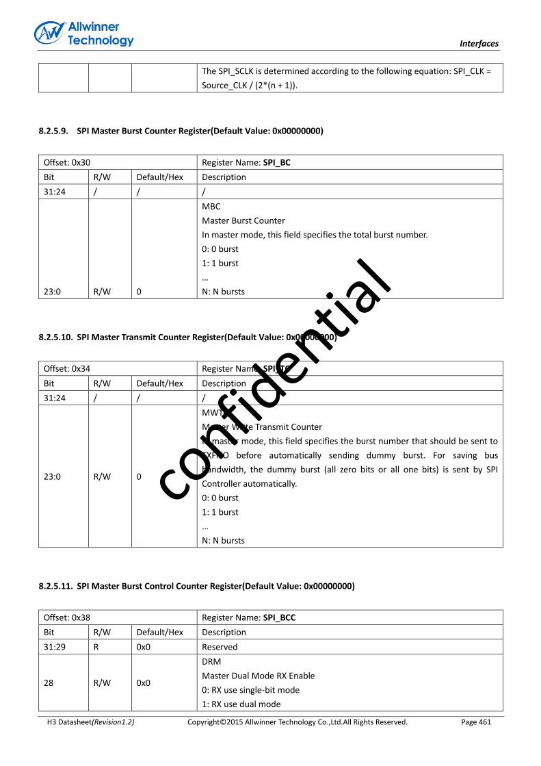
Interfaces
H3 Datasheet(Revision1.2) Copyright© 2015 Allwinner Technology Co.,Ltd.All Rights Reserved. Page 461
The SPI_SCLK is determined according to the following equation: SPI_CLK =
Source_CLK / (2*(n + 1)).
8.2.5.9. SPI Master Burst Counter Register(Default Value: 0x00000000)
Offset: 0x30 Register Name: SPI_BC
Bit R/W Default/Hex Description
31:24 / / /
23:0 R/W 0
MBC
Master Burst Counter
In master mode, this field specifies the total burst number.
0: 0 burst
1: 1 burst
…
N: N bursts
8.2.5.10. SPI Master Transmit Counter Register(Default Value: 0x00000000)
Offset: 0x34 Register Name: SPI_TC
Bit R/W Default/Hex Description
31:24 / / /
23:0 R/W 0
MWTC
Master Write Transmit Counter
In master mode, this field specifies the burst number that should be sent to
TXFIFO before automatically sending dummy burst. For saving bus
bandwidth, the dummy burst (all zero bits or all one bits) is sent by SPI
Controller automatically.
0: 0 burst
1: 1 burst
…
N: N bursts
8.2.5.11. SPI Master Burst Control Counter Register(Default Value: 0x00000000)
Offset: 0x38 Register Name: SPI_BCC
Bit R/W Default/Hex Description
31:29 R 0x0 Reserved
28 R/W 0x0
DRM
Master Dual Mode RX Enable
0: RX use single-bit mode
1: RX use dual mode
confid
ential

Interfaces
H3 Datasheet(Revision1.2) Copyright© 2015 Allwinner Technology Co.,Ltd.All Rights Reserved. Page 462
Note:Can’t be written when XCH=1.
27:24 R/W 0x0
DBC
Master Dummy Burst Counter
In master mode, this field specifies the burst number that should be sent
before receive in dual SPI mode. The data is don’t care by the device.
0: 0 burst
1: 1 burst
…
N: N bursts
Note:Can’t be written when XCH=1.
23:0 R/W 0x0
STC
Master Single Mode Transmit Counter
In master mode, this field specifies the burst number that should be sent in
single mode before automatically sending dummy burst. This is the first
transmit counter in all bursts.
0: 0 burst
1: 1 burst
…
N: N bursts
Note:Can’t be written when XCH=1.
8.2.5.12. SPI TX Data Register(Default Value: 0x00000000)
Offset: 0x200 Register Name: SPI_TXD
Bit R/W Default/Hex Description
31:0 W/R 0x0
TDATA
Transmit Data
This register can be accessed in byte, half-word or word unit by AHB. In byte
accessing method, if there are rooms in RXFIFO, one burst data is written to
RXFIFO and the depth is increased by 1. In half-word accessing method, two
SPI burst data are written and the TXFIFO depth is increase by 2. In word
accessing method, four SPI burst data are written and the TXFIFO depth is
increased by 4.
Note: This address is writing-only if TF_TEST is ‘0’, and if TF_TEST is set to ‘1’,
this address is readable and writable to test the TX FIFO through the AHB
bus.
8.2.5.13. SPI RX Data Register(Default Value: 0x00000000)
Offset: 0x300 Register Name: SPI_RXD
Bit R/W Default/Hex Description
31:0 R 0 RDATA
Receive Data
confid
ential

Interfaces
H3 Datasheet(Revision1.2) Copyright© 2015 Allwinner Technology Co.,Ltd.All Rights Reserved. Page 463
This register can be accessed in byte, half-word or word unit by AHB. In byte
accessing method, if there are data in RXFIFO, the top word is returned and
the RXFIFO depth is decreased by 1. In half-word accessing method, two SPI
bursts are returned and the RXFIFO depth is decrease by 2. In word
accessing method, the four SPI bursts are returned and the RXFIFO depth is
decreased by 4.
Note: This address is read-only if RF_TEST is ‘0’, and if RF_TEST is set to ‘1’,
this address is readable and writable to test the RX FIFO through the AHB
bus.
confid
ential

Interfaces
H3 Datasheet(Revision1.2) Copyright© 2015 Allwinner Technology Co.,Ltd.All Rights Reserved. Page 464
8.3. UART
8.3.1. Overview
The UART is used for serial communication with a peripheral, modem (data carrier equipment, DCE) or data set. Data is
written from a master (CPU) over the APB bus to the UART and it is converted to serial form and transmitted to the
destination device. Serial data is also received by the UART and stored for the master (CPU) to read back.
The UART contains registers to control the character length, baud rate, parity generation/checking, and interrupt
generation. Although there is only one interrupt output signal from the UART, there are several prioritized interrupt
types that can be responsible for its assertion. Each of the interrupt types can be separately enabled/disabled with the
control registers.
The UART has 16450 and 16550 modes of operation, which are compatible with a range of standard software drivers.
In 16550 mode, transmit and receive operations are both buffered by FIFOs. In 16450 mode, these FIFOs are disabled.
The UART supports data lengths from five to eight bits, an optional parity bit and 1, 1 ½ or 2 stop bits, and is fully
programmable by an AMBA APB CPU interface. A 16-bit programmable baud rate generator and an 8-bit scratch
register are included, together with separate transmit and receive FIFOs. Eight modem control lines and a diagnostic
loop-back mode are provided.
Interrupts can be generated for a range of TX Buffer/FIFO, RX Buffer/FIFO, Modem Status and Line Status conditions.
The UART includes the following features:
Compatible with industry-standard 16550 UARTs
64-Bytes Transmit and receive data FIFOs
DMA controller interface
Software/ Hardware Flow Control
Programmable Transmit Holding Register Empty interrupt
Interrupt support for FIFOs, Status Change
Support IrDA 1.0 SIR
8.3.2. UART Timing Diagram
Serial Data S Data bits 5-8 P S 1,1.5,2
One Character
Bit TimeBit Time
One Character
TX/RX
Figure 8-4. UART Serial Data Format
confid
ential
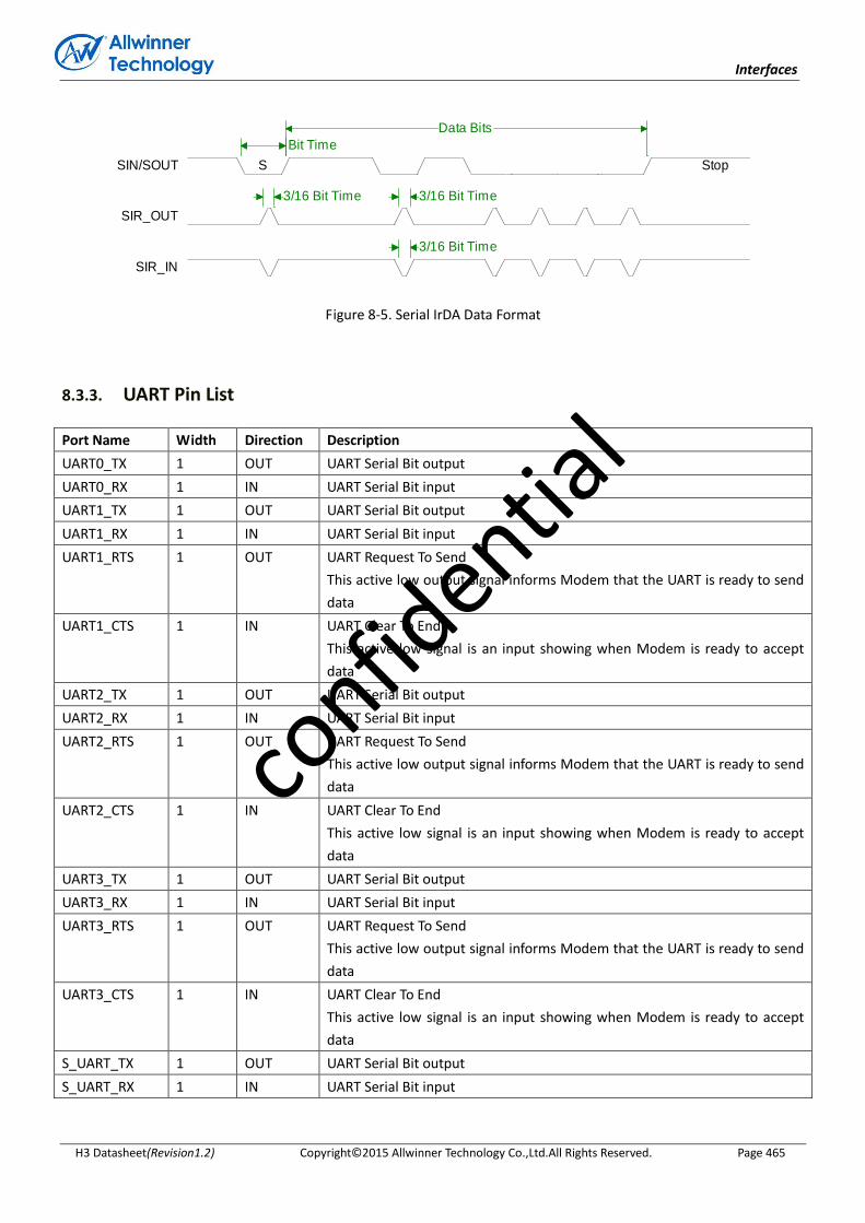
Interfaces
H3 Datasheet(Revision1.2) Copyright© 2015 Allwinner Technology Co.,Ltd.All Rights Reserved. Page 465
S Stop
3/16 Bit Time3/16 Bit Time
3/16 Bit Time3/16 Bit Time3/16 Bit Time3/16 Bit Time
Data Bits
Bit Time
Data Bits
Bit Time
SIN/SOUT
SIR_OUT
SIR_IN
Figure 8-5. Serial IrDA Data Format
8.3.3. UART Pin List
Port Name Width Direction Description
UART0_TX 1 OUT UART Serial Bit output
UART0_RX 1 IN UART Serial Bit input
UART1_TX 1 OUT UART Serial Bit output
UART1_RX 1 IN UART Serial Bit input
UART1_RTS 1 OUT UART Request To Send
This active low output signal informs Modem that the UART is ready to send
data
UART1_CTS 1 IN UART Clear To End
This active low signal is an input showing when Modem is ready to accept
data
UART2_TX 1 OUT UART Serial Bit output
UART2_RX 1 IN UART Serial Bit input
UART2_RTS 1 OUT UART Request To Send
This active low output signal informs Modem that the UART is ready to send
data
UART2_CTS 1 IN UART Clear To End
This active low signal is an input showing when Modem is ready to accept
data
UART3_TX 1 OUT UART Serial Bit output
UART3_RX 1 IN UART Serial Bit input
UART3_RTS 1 OUT UART Request To Send
This active low output signal informs Modem that the UART is ready to send
data
UART3_CTS 1 IN UART Clear To End
This active low signal is an input showing when Modem is ready to accept
data
S_UART_TX 1 OUT UART Serial Bit output
S_UART_RX 1 IN UART Serial Bit input
confid
ential
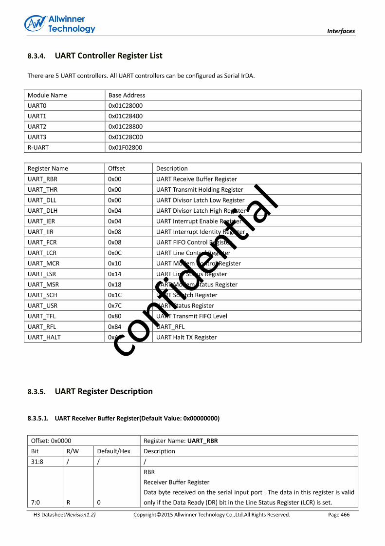
Interfaces
H3 Datasheet(Revision1.2) Copyright© 2015 Allwinner Technology Co.,Ltd.All Rights Reserved. Page 466
8.3.4. UART Controller Register List
There are 5 UART controllers. All UART controllers can be configured as Serial IrDA.
Module Name Base Address
UART0 0x01C28000
UART1 0x01C28400
UART2 0x01C28800
UART3 0x01C28C00
R-UART 0x01F02800
Register Name Offset Description
UART_RBR 0x00 UART Receive Buffer Register
UART_THR 0x00 UART Transmit Holding Register
UART_DLL 0x00 UART Divisor Latch Low Register
UART_DLH 0x04 UART Divisor Latch High Register
UART_IER 0x04 UART Interrupt Enable Register
UART_IIR 0x08 UART Interrupt Identity Register
UART_FCR 0x08 UART FIFO Control Register
UART_LCR 0x0C UART Line Control Register
UART_MCR 0x10 UART Modem Control Register
UART_LSR 0x14 UART Line Status Register
UART_MSR 0x18 UART Modem Status Register
UART_SCH 0x1C UART Scratch Register
UART_USR 0x7C UART Status Register
UART_TFL 0x80 UART Transmit FIFO Level
UART_RFL 0x84 UART_RFL
UART_HALT 0xA4 UART Halt TX Register
8.3.5. UART Register Description
8.3.5.1. UART Receiver Buffer Register(Default Value: 0x00000000)
Offset: 0x0000 Register Name: UART_RBR
Bit R/W Default/Hex Description
31:8 / / /
7:0 R 0
RBR
Receiver Buffer Register
Data byte received on the serial input port . The data in this register is valid
only if the Data Ready (DR) bit in the Line Status Register (LCR) is set.
confid
ential
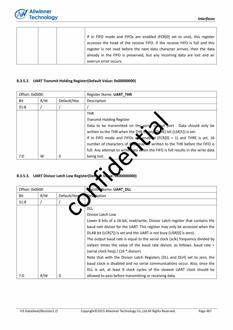
Interfaces
H3 Datasheet(Revision1.2) Copyright© 2015 Allwinner Technology Co.,Ltd.All Rights Reserved. Page 467
If in FIFO mode and FIFOs are enabled (FCR[0] set to one), this register
accesses the head of the receive FIFO. If the receive FIFO is full and this
register is not read before the next data character arrives, then the data
already in the FIFO is preserved, but any incoming data are lost and an
overrun error occurs.
8.3.5.2. UART Transmit Holding Register(Default Value: 0x00000000)
Offset: 0x0000 Register Name: UART_THR
Bit R/W Default/Hex Description
31:8 / / /
7:0 W 0
THR
Transmit Holding Register
Data to be transmitted on the serial output port . Data should only be
written to the THR when the THR Empty (THRE) bit (LSR[5]) is set.
If in FIFO mode and FIFOs are enabled (FCR[0] = 1) and THRE is set, 16
number of characters of data may be written to the THR before the FIFO is
full. Any attempt to write data when the FIFO is full results in the write data
being lost.
8.3.5.3. UART Divisor Latch Low Register(Default Value: 0x00000000)
Offset: 0x0000 Register Name: UART_DLL
Bit R/W Default/Hex Description
31:8 / / /
7:0 R/W 0
DLL
Divisor Latch Low
Lower 8 bits of a 16-bit, read/write, Divisor Latch register that contains the
baud rate divisor for the UART. This register may only be accessed when the
DLAB bit (LCR[7]) is set and the UART is not busy (USR[0] is zero).
The output baud rate is equal to the serial clock (sclk) frequency divided by
sixteen times the value of the baud rate divisor, as follows: baud rate =
(serial clock freq) / (16 * divisor).
Note that with the Divisor Latch Registers (DLL and DLH) set to zero, the
baud clock is disabled and no serial communications occur. Also, once the
DLL is set, at least 8 clock cycles of the slowest UART clock should be
allowed to pass before transmitting or receiving data.
confid
ential
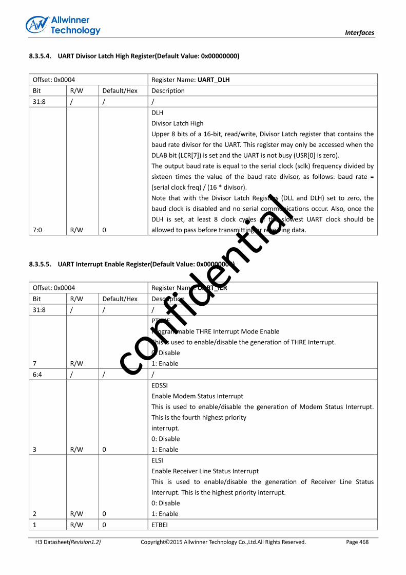
Interfaces
H3 Datasheet(Revision1.2) Copyright© 2015 Allwinner Technology Co.,Ltd.All Rights Reserved. Page 468
8.3.5.4. UART Divisor Latch High Register(Default Value: 0x00000000)
Offset: 0x0004 Register Name: UART_DLH
Bit R/W Default/Hex Description
31:8 / / /
7:0 R/W 0
DLH
Divisor Latch High
Upper 8 bits of a 16-bit, read/write, Divisor Latch register that contains the
baud rate divisor for the UART. This register may only be accessed when the
DLAB bit (LCR[7]) is set and the UART is not busy (USR[0] is zero).
The output baud rate is equal to the serial clock (sclk) frequency divided by
sixteen times the value of the baud rate divisor, as follows: baud rate =
(serial clock freq) / (16 * divisor).
Note that with the Divisor Latch Registers (DLL and DLH) set to zero, the
baud clock is disabled and no serial communications occur. Also, once the
DLH is set, at least 8 clock cycles of the slowest UART clock should be
allowed to pass before transmitting or receiving data.
8.3.5.5. UART Interrupt Enable Register(Default Value: 0x00000000)
Offset: 0x0004 Register Name: UART_IER
Bit R/W Default/Hex Description
31:8 / / /
7 R/W
PTIME
Programmable THRE Interrupt Mode Enable
This is used to enable/disable the generation of THRE Interrupt.
0: Disable
1: Enable
6:4 / / /
3 R/W 0
EDSSI
Enable Modem Status Interrupt
This is used to enable/disable the generation of Modem Status Interrupt.
This is the fourth highest priority
interrupt.
0: Disable
1: Enable
2 R/W 0
ELSI
Enable Receiver Line Status Interrupt
This is used to enable/disable the generation of Receiver Line Status
Interrupt. This is the highest priority interrupt.
0: Disable
1: Enable
1 R/W 0 ETBEI
confid
ential

Interfaces
H3 Datasheet(Revision1.2) Copyright© 2015 Allwinner Technology Co.,Ltd.All Rights Reserved. Page 469
Enable Transmit Holding Register Empty Interrupt
This is used to enable/disable the generation of Transmitter Holding Register
Empty Interrupt. This is the third highest priority interrupt.
0: Disable
1: Enable
0 R/W 0
ERBFI
Enable Received Data Available Interrupt
This is used to enable/disable the generation of Received Data Available
Interrupt and the Character Timeout Interrupt (if in FIFO mode and FIFOs
enabled). These are the second highest priority interrupts.
0: Disable
1: Enable
8.3.5.6. UART Interrupt Identity Register(Default Value: 0x00000000)
Offset: 0x0008 Register Name: UART_IIR
Bit R/W Default/Hex Description
31:8 / / /
7:6 R 0
FEFLAG
FIFOs Enable Flag
This is used to indicate whether the FIFOs are enabled or disabled.
00: Disable
11: Enable
5:4 / / /
3:0 R 0x1
IID
Interrupt ID
This indicates the highest priority pending interrupt which can be one of the
following types:
0000: modem status
0001: no interrupt pending
0010: THR empty
0100: received data available
0110: receiver line status
0111: busy detect
1100: character timeout
Bit 3 indicates an interrupt can only occur when the FIFOs are enabled and
used to distinguish a Character Timeout condition interrupt.
Interru
pt ID
Priority
Level
Interrupt Type Interrupt Source Interrupt Reset
0001 - None None -
0110 Highest Receiver line
status
Overrun/parity/ framing errors
or break interrupt
Reading the line status register
confid
ential
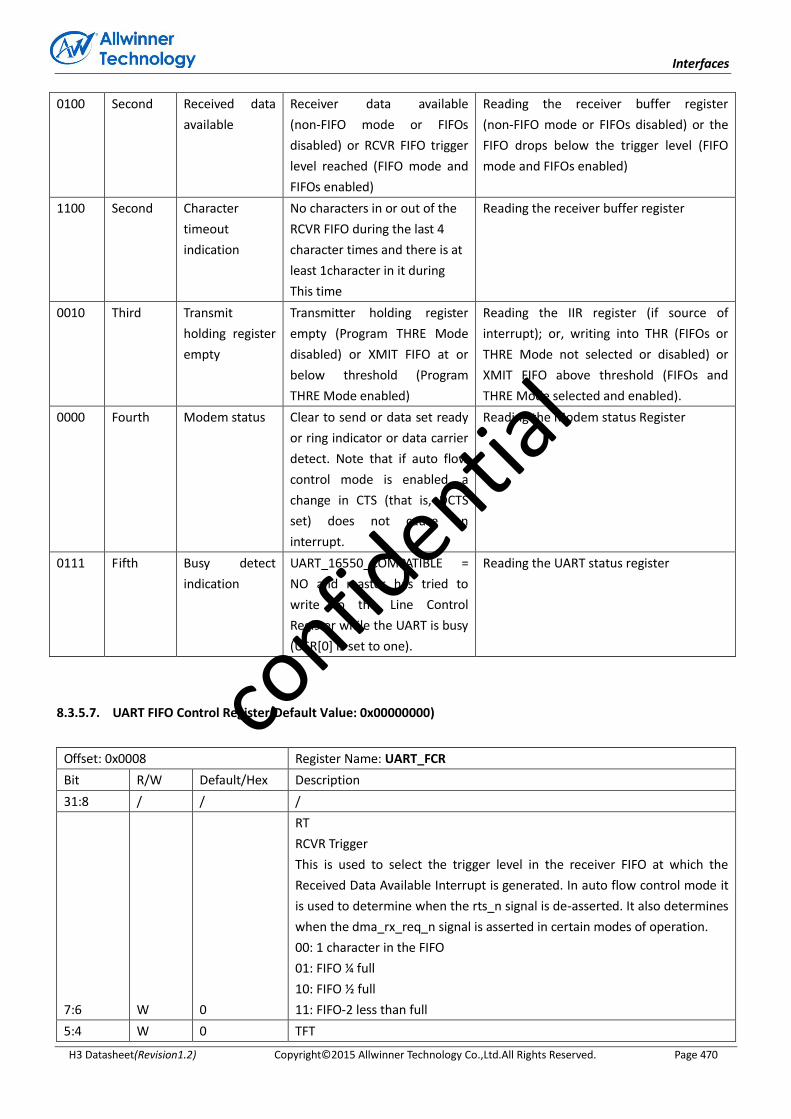
Interfaces
H3 Datasheet(Revision1.2) Copyright© 2015 Allwinner Technology Co.,Ltd.All Rights Reserved. Page 470
0100 Second Received data
available
Receiver data available
(non-FIFO mode or FIFOs
disabled) or RCVR FIFO trigger
level reached (FIFO mode and
FIFOs enabled)
Reading the receiver buffer register
(non-FIFO mode or FIFOs disabled) or the
FIFO drops below the trigger level (FIFO
mode and FIFOs enabled)
1100 Second Character
timeout
indication
No characters in or out of the
RCVR FIFO during the last 4
character times and there is at
least 1character in it during
This time
Reading the receiver buffer register
0010 Third Transmit
holding register
empty
Transmitter holding register
empty (Program THRE Mode
disabled) or XMIT FIFO at or
below threshold (Program
THRE Mode enabled)
Reading the IIR register (if source of
interrupt); or, writing into THR (FIFOs or
THRE Mode not selected or disabled) or
XMIT FIFO above threshold (FIFOs and
THRE Mode selected and enabled).
0000 Fourth Modem status Clear to send or data set ready
or ring indicator or data carrier
detect. Note that if auto flow
control mode is enabled, a
change in CTS (that is, DCTS
set) does not cause an
interrupt.
Reading the Modem status Register
0111 Fifth Busy detect
indication
UART_16550_COMPATIBLE =
NO and master has tried to
write to the Line Control
Register while the UART is busy
(USR[0] is set to one).
Reading the UART status register
8.3.5.7. UART FIFO Control Register(Default Value: 0x00000000)
Offset: 0x0008 Register Name: UART_FCR
Bit R/W Default/Hex Description
31:8 / / /
7:6 W 0
RT
RCVR Trigger
This is used to select the trigger level in the receiver FIFO at which the
Received Data Available Interrupt is generated. In auto flow control mode it
is used to determine when the rts_n signal is de-asserted. It also determines
when the dma_rx_req_n signal is asserted in certain modes of operation.
00: 1 character in the FIFO
01: FIFO ¼ full
10: FIFO ½ full
11: FIFO-2 less than full
5:4 W 0 TFT
confid
ential
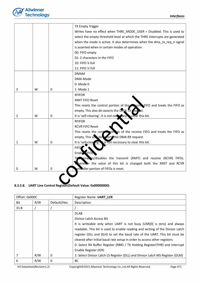
Interfaces
H3 Datasheet(Revision1.2) Copyright© 2015 Allwinner Technology Co.,Ltd.All Rights Reserved. Page 471
TX Empty Trigger
Writes have no effect when THRE_MODE_USER = Disabled. This is used to
select the empty threshold level at which the THRE Interrupts are generated
when the mode is active. It also determines when the dma_tx_req_n signal
is asserted when in certain modes of operation.
00: FIFO empty
01: 2 characters in the FIFO
10: FIFO ¼ full
11: FIFO ½ full
3 W 0
DMAM
DMA Mode
0: Mode 0
1: Mode 1
2 W 0
XFIFOR
XMIT FIFO Reset
This resets the control portion of the transmit FIFO and treats the FIFO as
empty. This also de-asserts the DMA TX request.
It is 'self-clearing'. It is not necessary to clear this bit.
1 W 0
RFIFOR
RCVR FIFO Reset
This resets the control portion of the receive FIFO and treats the FIFO as
empty. This also de-asserts the DMA RX request.
It is 'self-clearing'. It is not necessary to clear this bit.
0 W 0
FIFOE
Enable FIFOs
This enables/disables the transmit (XMIT) and receive (RCVR) FIFOs.
Whenever the value of this bit is changed both the XMIT and RCVR
controller portion of FIFOs is reset.
8.3.5.8. UART Line Control Register(Default Value: 0x00000000)
Offset: 0x000C Register Name: UART_LCR
Bit R/W Default/Hex Description
31:8 / / /
7 R/W 0
DLAB
Divisor Latch Access Bit
It is writeable only when UART is not busy (USR[0] is zero) and always
readable. This bit is used to enable reading and writing of the Divisor Latch
register (DLL and DLH) to set the baud rate of the UART. This bit must be
cleared after initial baud rate setup in order to access other registers.
0: Select RX Buffer Register (RBR) / TX Holding Register(THR) and Interrupt
Enable Register (IER)
1: Select Divisor Latch LS Register (DLL) and Divisor Latch MS Register (DLM)
6 R/W 0 BC
confid
ential

Interfaces
H3 Datasheet(Revision1.2) Copyright© 2015 Allwinner Technology Co.,Ltd.All Rights Reserved. Page 472
Break Control Bit
This is used to cause a break condition to be transmitted to the receiving
device. If set to one the serial output is forced to the spacing (logic 0) state.
When not in Loopback Mode, as determined by MCR[4], the sout line is
forced low until the Break bit is cleared. If SIR_MODE = Enabled and active
(MCR[6] set to one) the sir_out_n line is continuously pulsed. When in
Loopback Mode, the break condition is internally looped back to the
receiver and the sir_out_n line is forced low.
5:4 R/W 0
EPS
Even Parity Select
It is writeable only when UART is not busy (USR[0] is zero) and always
writable readable. This is used to select between even and odd parity, when
parity is enabled (PEN set to one). Setting the LCR[5] is to reverse the LCR[4].
00: Odd Parity
01: Even Parity
1X: Reverse LCR[4]
3 R/W 0
PEN
Parity Enable
It is writeable only when UART is not busy (USR[0] is zero) and always
readable. This bit is used to enable and disable parity generation and
detection in transmitted and received serial character respectively.
0: parity disabled
1: parity enabled
2 R/W 0
STOP
Number of stop bits
It is writeable only when UART is not busy (USR[0] is zero) and always
readable. This is used to select the number of stop bits per character that
the peripheral transmits and receives. If set to zero, one stop bit is
transmitted in the serial data. If set to one and the data bits are set to 5
(LCR[1:0] set to zero) one and a half stop bits is transmitted. Otherwise, two
stop bits are transmitted. Note that regardless of the number of stop bits
selected, the receiver checks only the first stop bit.
0: 1 stop bit
1: 1.5 stop bits when DLS (LCR[1:0]) is zero, else 2 stop bit
1:0 R/W 0
DLS
Data Length Select
It is writeable only when UART is not busy (USR[0] is zero) and always
readable. This is used to select the number of data bits per character that
the peripheral transmits and receives. The number of bit that may be
selected areas follows:
00: 5 bits
01: 6 bits
10: 7 bits
11: 8 bits
confid
ential

Interfaces
H3 Datasheet(Revision1.2) Copyright© 2015 Allwinner Technology Co.,Ltd.All Rights Reserved. Page 473
8.3.5.9. UART Modem Control Register(Default Value: 0x00000000)
Offset: 0x0010 Register Name: UART_MCR
Bit R/W Default/Hex Description
31:6 / / /
5 R/W 0
AFCE
Auto Flow Control Enable
When FIFOs are enabled and the Auto Flow Control Enable (AFCE) bit is set,
Auto Flow Control features are enabled.
0: Auto Flow Control Mode disabled
1: Auto Flow Control Mode enabled
4 R/W 0
LOOP
Loop Back Mode
0: Normal Mode
1: Loop Back Mode
This is used to put the UART into a diagnostic mode for test purposes. If
operating in UART mode (SIR_MODE != Enabled or not active, MCR[6] set to
zero), data on the sout line is held high, while serial data output is looped
back to the sin line, internally. In this mode all the interrupts are fully
functional. Also, in loopback mode, the modem control inputs (dsr_n, cts_n,
ri_n, dcd_n) are disconnected and the modem control outputs (dtr_n, rts_n,
out1_n, out2_n) are looped back to the inputs, internally. If operating in
infrared mode (SIR_MODE == Enabled AND active, MCR[6] set to one), data
on the sir_out_n line is held low, while serial data output is inverted and
looped back to the sir_in line.
3:2 / / /
1 R/W 0
RTS
Request to Send
This is used to directly control the Request to Send (rts_n) output. The
Request To Send (rts_n) output is used to inform the modem or data set that
the UART is ready to exchange data. When Auto RTS Flow Control is not
enabled (MCR[5] set to zero), the rts_n signal is set low by programming
MCR[1] (RTS) to a high.In Auto Flow Control, AFCE_MODE == Enabled and
active (MCR[5] set to one) and FIFOs enable (FCR[0] set to one), the rts_n
output is controlled in the same way, but is also gated with the receiver FIFO
threshold trigger (rts_n is inactive high when above the threshold). The
rts_n signal is de-asserted when MCR[1] is set low.
0: rts_n de-asserted (logic 1)
1: rts_n asserted (logic 0)
Note that in Loopback mode (MCR[4] set to one), the rts_n output is held
inactive high while the value of this location is internally looped back to an
input.
0 R/W 0
DTR
Data Terminal Ready
This is used to directly control the Data Terminal Ready (dtr_n) output. The
confid
ential
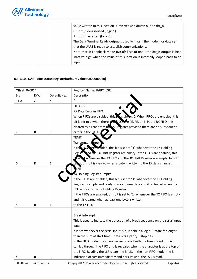
Interfaces
H3 Datasheet(Revision1.2) Copyright© 2015 Allwinner Technology Co.,Ltd.All Rights Reserved. Page 474
value written to this location is inverted and driven out on dtr_n.
0:dtr_n de-asserted (logic 1)
1:dtr_n asserted (logic 0)
The Data Terminal Ready output is used to inform the modem or data set
that the UART is ready to establish communications.
Note that in Loopback mode (MCR[4] set to one), the dtr_n output is held
inactive high while the value of this location is internally looped back to an
input.
8.3.5.10. UART Line Status Register(Default Value: 0x00000060)
Offset: 0x0014 Register Name: UART_LSR
Bit R/W Default/Hex Description
31:8 / / /
7 R 0
FIFOERR
RX Data Error in FIFO
When FIFOs are disabled, this bit is always 0. When FIFOs are enabled, this
bit is set to 1 when there is at least one PE, FE, or BI in the RX FIFO. It is
cleared by a read from the LSR register provided there are no subsequent
errors in the FIFO.
6 R 1
TEMT
Transmitter Empty
If the FIFOs are disabled, this bit is set to "1" whenever the TX Holding
Register and the TX Shift Register are empty. If the FIFOs are enabled, this
bit is set whenever the TX FIFO and the TX Shift Register are empty. In both
cases, this bit is cleared when a byte is written to the TX data channel.
5 R 1
THRE
TX Holding Register Empty
If the FIFOs are disabled, this bit is set to "1" whenever the TX Holding
Register is empty and ready to accept new data and it is cleared when the
CPU writes to the TX Holding Register.
If the FIFOs are enabled, this bit is set to "1" whenever the TX FIFO is empty
and it is cleared when at least one byte is written
to the TX FIFO.
4 R 0
BI
Break Interrupt
This is used to indicate the detection of a break sequence on the serial input
data.
It is set whenever the serial input, sin, is held in a logic '0' state for longer
than the sum of start time + data bits + parity + stop bits.
In the FIFO mode, the character associated with the break condition is
carried through the FIFO and is revealed when the character is at the top of
the FIFO. Reading the LSR clears the BI bit. In the non-FIFO mode, the BI
indication occurs immediately and persists until the LSR is read.
confid
ential
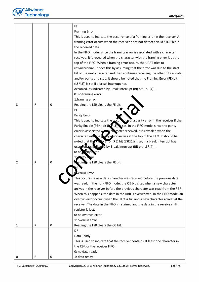
Interfaces
H3 Datasheet(Revision1.2) Copyright© 2015 Allwinner Technology Co.,Ltd.All Rights Reserved. Page 475
3 R 0
FE
Framing Error
This is used to indicate the occurrence of a framing error in the receiver. A
framing error occurs when the receiver does not detect a valid STOP bit in
the received data.
In the FIFO mode, since the framing error is associated with a character
received, it is revealed when the character with the framing error is at the
top of the FIFO. When a framing error occurs, the UART tries to
resynchronize. It does this by assuming that the error was due to the start
bit of the next character and then continues receiving the other bit i.e. data,
and/or parity and stop. It should be noted that the Framing Error (FE) bit
(LSR[3]) is set if a break interrupt has
occurred, as indicated by Break Interrupt (BI) bit (LSR[4]).
0: no framing error
1:framing error
Reading the LSR clears the FE bit.
2 R 0
PE
Parity Error
This is used to indicate the occurrence of a parity error in the receiver if the
Parity Enable (PEN) bit (LCR[3]) is set. In the FIFO mode, since the parity
error is associated with a character received, it is revealed when the
character with the parity error arrives at the top of the FIFO. It should be
noted that the Parity Error (PE) bit (LSR[2]) is set if a break interrupt has
occurred, as indicated by Break Interrupt (BI) bit (LSR[4]).
0: no parity error
1: parity error
Reading the LSR clears the PE bit.
1 R 0
OE
Overrun Error
This occurs if a new data character was received before the previous data
was read. In the non-FIFO mode, the OE bit is set when a new character
arrives in the receiver before the previous character was read from the RBR.
When this happens, the data in the RBR is overwritten. In the FIFO mode, an
overrun error occurs when the FIFO is full and a new character arrives at the
receiver. The data in the FIFO is retained and the data in the receive shift
register is lost.
0: no overrun error
1: overrun error
Reading the LSR clears the OE bit.
0 R 0
DR
Data Ready
This is used to indicate that the receiver contains at least one character in
the RBR or the receiver FIFO.
0: no data ready
1: data ready
confid
ential
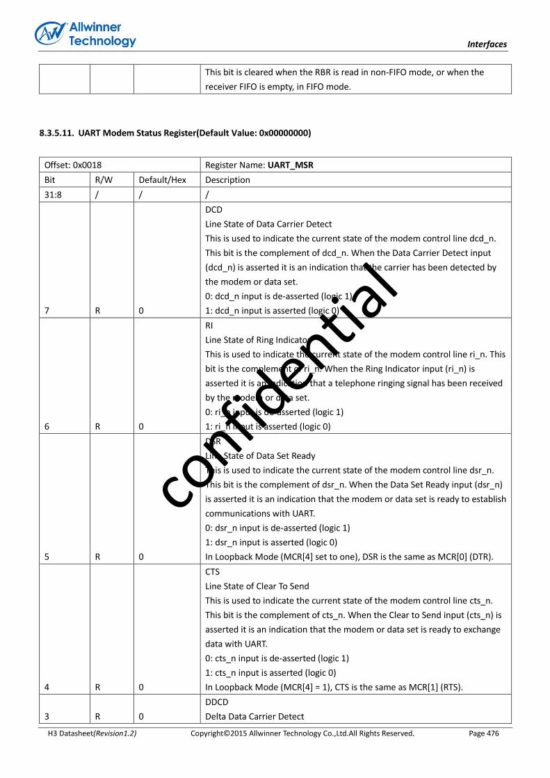
Interfaces
H3 Datasheet(Revision1.2) Copyright© 2015 Allwinner Technology Co.,Ltd.All Rights Reserved. Page 476
This bit is cleared when the RBR is read in non-FIFO mode, or when the
receiver FIFO is empty, in FIFO mode.
8.3.5.11. UART Modem Status Register(Default Value: 0x00000000)
Offset: 0x0018 Register Name: UART_MSR
Bit R/W Default/Hex Description
31:8 / / /
7 R 0
DCD
Line State of Data Carrier Detect
This is used to indicate the current state of the modem control line dcd_n.
This bit is the complement of dcd_n. When the Data Carrier Detect input
(dcd_n) is asserted it is an indication that the carrier has been detected by
the modem or data set.
0: dcd_n input is de-asserted (logic 1)
1: dcd_n input is asserted (logic 0)
6 R 0
RI
Line State of Ring Indicator
This is used to indicate the current state of the modem control line ri_n. This
bit is the complement of ri_n. When the Ring Indicator input (ri_n) is
asserted it is an indication that a telephone ringing signal has been received
by the modem or data set.
0: ri_n input is de-asserted (logic 1)
1: ri_n input is asserted (logic 0)
5 R 0
DSR
Line State of Data Set Ready
This is used to indicate the current state of the modem control line dsr_n.
This bit is the complement of dsr_n. When the Data Set Ready input (dsr_n)
is asserted it is an indication that the modem or data set is ready to establish
communications with UART.
0: dsr_n input is de-asserted (logic 1)
1: dsr_n input is asserted (logic 0)
In Loopback Mode (MCR[4] set to one), DSR is the same as MCR[0] (DTR).
4 R 0
CTS
Line State of Clear To Send
This is used to indicate the current state of the modem control line cts_n.
This bit is the complement of cts_n. When the Clear to Send input (cts_n) is
asserted it is an indication that the modem or data set is ready to exchange
data with UART.
0: cts_n input is de-asserted (logic 1)
1: cts_n input is asserted (logic 0)
In Loopback Mode (MCR[4] = 1), CTS is the same as MCR[1] (RTS).
3 R 0
DDCD
Delta Data Carrier Detect
confid
ential
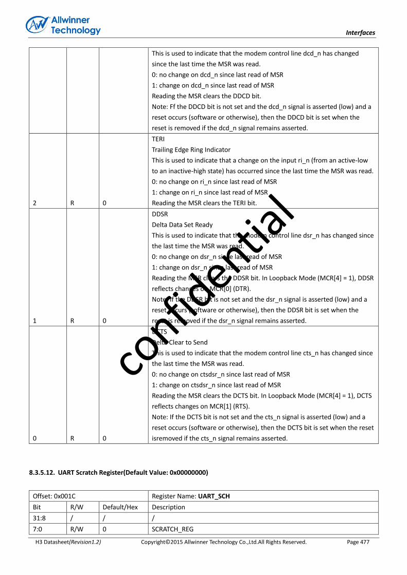
Interfaces
H3 Datasheet(Revision1.2) Copyright© 2015 Allwinner Technology Co.,Ltd.All Rights Reserved. Page 477
This is used to indicate that the modem control line dcd_n has changed
since the last time the MSR was read.
0: no change on dcd_n since last read of MSR
1: change on dcd_n since last read of MSR
Reading the MSR clears the DDCD bit.
Note: Ff the DDCD bit is not set and the dcd_n signal is asserted (low) and a
reset occurs (software or otherwise), then the DDCD bit is set when the
reset is removed if the dcd_n signal remains asserted.
2 R 0
TERI
Trailing Edge Ring Indicator
This is used to indicate that a change on the input ri_n (from an active-low
to an inactive-high state) has occurred since the last time the MSR was read.
0: no change on ri_n since last read of MSR
1: change on ri_n since last read of MSR
Reading the MSR clears the TERI bit.
1 R 0
DDSR
Delta Data Set Ready
This is used to indicate that the modem control line dsr_n has changed since
the last time the MSR was read.
0: no change on dsr_n since last read of MSR
1: change on dsr_n since last read of MSR
Reading the MSR clears the DDSR bit. In Loopback Mode (MCR[4] = 1), DDSR
reflects changes on MCR[0] (DTR).
Note: If the DDSR bit is not set and the dsr_n signal is asserted (low) and a
reset occurs (software or otherwise), then the DDSR bit is set when the
reset is removed if the dsr_n signal remains asserted.
0 R 0
DCTS
Delta Clear to Send
This is used to indicate that the modem control line cts_n has changed since
the last time the MSR was read.
0: no change on ctsdsr_n since last read of MSR
1: change on ctsdsr_n since last read of MSR
Reading the MSR clears the DCTS bit. In Loopback Mode (MCR[4] = 1), DCTS
reflects changes on MCR[1] (RTS).
Note: If the DCTS bit is not set and the cts_n signal is asserted (low) and a
reset occurs (software or otherwise), then the DCTS bit is set when the reset
isremoved if the cts_n signal remains asserted.
8.3.5.12. UART Scratch Register(Default Value: 0x00000000)
Offset: 0x001C Register Name: UART_SCH
Bit R/W Default/Hex Description
31:8 / / /
7:0 R/W 0 SCRATCH_REG
confid
ential
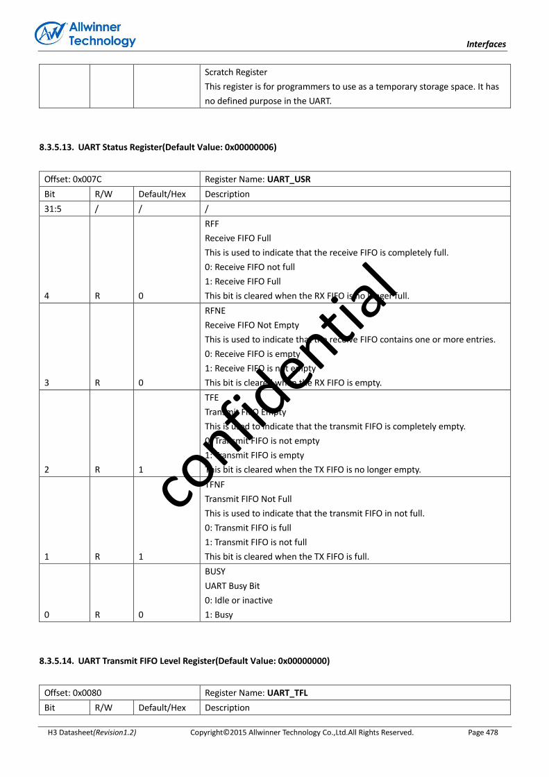
Interfaces
H3 Datasheet(Revision1.2) Copyright© 2015 Allwinner Technology Co.,Ltd.All Rights Reserved. Page 478
Scratch Register
This register is for programmers to use as a temporary storage space. It has
no defined purpose in the UART.
8.3.5.13. UART Status Register(Default Value: 0x00000006)
Offset: 0x007C Register Name: UART_USR
Bit R/W Default/Hex Description
31:5 / / /
4 R 0
RFF
Receive FIFO Full
This is used to indicate that the receive FIFO is completely full.
0: Receive FIFO not full
1: Receive FIFO Full
This bit is cleared when the RX FIFO is no longer full.
3 R 0
RFNE
Receive FIFO Not Empty
This is used to indicate that the receive FIFO contains one or more entries.
0: Receive FIFO is empty
1: Receive FIFO is not empty
This bit is cleared when the RX FIFO is empty.
2 R 1
TFE
Transmit FIFO Empty
This is used to indicate that the transmit FIFO is completely empty.
0: Transmit FIFO is not empty
1: Transmit FIFO is empty
This bit is cleared when the TX FIFO is no longer empty.
1 R 1
TFNF
Transmit FIFO Not Full
This is used to indicate that the transmit FIFO in not full.
0: Transmit FIFO is full
1: Transmit FIFO is not full
This bit is cleared when the TX FIFO is full.
0 R 0
BUSY
UART Busy Bit
0: Idle or inactive
1: Busy
8.3.5.14. UART Transmit FIFO Level Register(Default Value: 0x00000000)
Offset: 0x0080 Register Name: UART_TFL
Bit R/W Default/Hex Description
confid
ential

Interfaces
H3 Datasheet(Revision1.2) Copyright© 2015 Allwinner Technology Co.,Ltd.All Rights Reserved. Page 479
31:7 / / /
6:0 R 0
TFL
Transmit FIFO Level
This is indicates the number of data entries in the transmit FIFO.
8.3.5.15. UART Receive FIFO Level Register(Default Value: 0x00000000)
Offset: 0x0084 Register Name: UART_RFL
Bit R/W Default/Hex Description
31:7 / / /
6:0 R 0
RFL
Receive FIFO Level
This is indicates the number of data entries in the receive FIFO.
8.3.5.16. UART Halt TX Register(Default Value: 0x00000000)
Offset: 0x00A4 Register Name: UART_HALT
Bit R/W Default/Hex Description
31:4 / / /
5 R/W 0
SIR_RX_INVERT
SIR Receiver Pulse Polarity Invert
0: Not invert receiver signal
1: Invert receiver signal
4 R/W 0
SIR_TX_INVERT
SIR Transmit Pulse Polarity Invert
0: Not invert transmit pulse
1: Invert transmit pulse
3 / / /
2 R/W 0
CHANGE_UPDATE
After the user using HALT[1] to change the baudrate or LCR configuration,
write 1 to update the configuration and waiting this bit self clear to 0 to
finish update process. Write 0 to this bit has no effect.
1: Update trigger, Self clear to 0 when finish update.
1 R/W 0
CHCFG_AT_BUSY
This is an enable bit for the user to change LCR register configuration
(except for the DLAB bit) and baudrate register (DLH and DLL) when the
UART is busy (USB[0] is 1).
1: Enable change when busy
0 R/W 0
HALT_TX
Halt TX
This register is use to halt transmissions for testing, so that the transmit FIFO
can be filled by the master when FIFOs are implemented and enabled.
confid
ential

Interfaces
H3 Datasheet(Revision1.2) Copyright© 2015 Allwinner Technology Co.,Ltd.All Rights Reserved. Page 480
0 : Halt TX disabled
1 : Halt TX enabled
Note: If FIFOs are not enabled, the setting of the halt TX register has no
effect on operation.
confid
ential
Interfaces
H3 Datasheet(Revision1.2) Copyright© 2015 Allwinner Technology Co.,Ltd.All Rights Reserved. Page 481
8.4. CIR Receiver
8.4.1. Overview
The CIR includes the following features:
Full physical layer implementation
Support CIR for remote control
64x8 bits FIFO for data buffer
Programmable FIFO thresholds
For saving CPU resource, CIR receiver is implemented in hardware. The CIR receiver samples the input signal on the
programmable frequency and records these samples into RX FIFO when one CIR signal is found on the air. The CIR
receiver uses Run-Length Code (RLC) to encode pulse width. The encoded data is buffered in a 64 levels and 8-bit width
RX FIFO; the MSB bit is used to record the polarity of the receiving CIR signal. The high level is represented as ‘1’ and the
low level is represented as ‘0’. The rest 7 bits are used for the length of RLC. The maximum length is 128. If the duration
of one level (high or low level) is more than 128, another byte is used.
In the air, there is always some noise. One threshold can be set to filter the noise to reduce system loading and improve
the system stability.
8.4.2. CIR Receiver Register List
Module Name Base Address
CIR 0x01F02000
Register Name Offset Description
CIR_CTL 0x00 CIR Control Register
CIR_RXCTL 0x10 CIR Receiver Configure Register
CIR_RXFIFO 0x20 CIR Receiver FIFO Register
CIR_RXINT 0x2C CIR Receiver Interrupt Control Register
CIR_RXSTA 0x30 CIR Receiver Status Register
CIR_CONFIG 0x34 CIR Configure Register
confid
ential

Interfaces
H3 Datasheet(Revision1.2) Copyright© 2015 Allwinner Technology Co.,Ltd.All Rights Reserved. Page 482
8.4.3. CIR Receiver Register Description
8.4.3.1. CIR Receiver Control Register(Default Value: 0x00000000)
Offset: 0x0000 Register Name: CIR_CTL
Bit R/W Default/Hex Description
31:9 / / /
8 R/W 0
CGPO
General Program Output (GPO) Control in CIR mode for TX Pin
0: Low level
1: High level
7:6 / / /
5:4 R/W 0
CIR ENABLE
00~10: Reserved
11: CIR mode enable
3:2 / / /.
1 R/W 0
RXEN
Receiver Block Enable
0: Disable
1: Enable
0 R/W 0
GEN
Global Enable
A disable on this bit overrides any other block or channel enables and
flushes all FIFOs.
0: Disable
1: Enable
8.4.3.2. CIR Receiver Configure Register(Default Value: 0x00000004)
Offset: 0x0010 Register Name: CIR_RXCTL
Bit R/W Default/Hex Description
31:3 / / /
2 R/W 1
RPPI
Receiver Pulse Polarity Invert
0: Not invert receiver signal
1: Invert receiver signal
1:0 / / /
8.4.3.3. CIR Receiver FIFO Register(Default Value: 0x00000000)
Offset: 0x0020 Register Name: CIR_RXFIFO
confid
ential

Interfaces
H3 Datasheet(Revision1.2) Copyright© 2015 Allwinner Technology Co.,Ltd.All Rights Reserved. Page 483
Bit R/W Default/Hex Description
31:8 / / /
7:0 R 0 Receiver Byte FIFO
8.4.3.4. CIR Receiver Interrupt Control Register(Default Value: 0x00000000)
Offset: 0x002C Register Name: CIR_RXINT
Bit R/W Default/Hex Description
31:14 / / /
13:8 R/W 0
RAL
RX FIFO Available Received Byte Level for interrupt and DMA request
TRIGGER_LEVEL = RAL + 1
5 R/W 0
DRQ_EN
RX FIFO DMA Enable
0: Disable
1: Enable
When set to ‘1’, the Receiver FIFO DRQ is asserted if reaching RAL. The DRQ
is de-asserted when condition fails.
4 R/W 0
RAI_EN
RX FIFO Available Interrupt Enable
0: Disable
1: Enable
When set to ‘1’, the Receiver FIFO IRQ is asserted if reaching RAL. The IRQ is
de-asserted when condition fails.
3:2 / / /
1 R/W 0
RPEI_EN
Receiver Packet End Interrupt Enable
0: Disable
1: Enable
0 R/W 0
ROI_EN
Receiver FIFO Overrun Interrupt Enable
0: Disable
1: Enable
8.4.3.5. CIR Receiver Status Register(Default Value: 0x00000000)
Offset: 0x0030 Register Name: CIR_RXSTA
Bit R/W Default/Hex Description
31:15 / / /
14:8 R 0
RAC
RX FIFO Available Counter
0: No available data in RX FIFO
confid
ential
Interfaces
H3 Datasheet(Revision1.2) Copyright© 2015 Allwinner Technology Co.,Ltd.All Rights Reserved. Page 484
1: 1 byte available data in RX FIFO
2: 2 byte available data in RX FIFO
…
64: 64 byte available data in RX FIFO
7 R 0x0
STAT
Status of CIR
0x0 – Idle
0x1 – busy
6:5 / / /
4 R/W 0
RA
RX FIFO Available
0: RX FIFO not available according its level
1: RX FIFO available according its level
This bit is cleared by writing a ‘1’.
3:2 / / /
1 R/W 0
RPE
Receiver Packet End Flag
0: STO was not detected. In CIR mode, one CIR symbol is receiving or not
detected.
1: STO field or packet abort symbol (7’b0000,000 and 8’b0000,0000 for MIR
and FIR) is detected. In CIR mode, one CIR symbol is received.
This bit is cleared by writing a ‘1’.
0 R/W 0
ROI
Receiver FIFO Overrun
0: Receiver FIFO not overrun
1: Receiver FIFO overrun
This bit is cleared by writing a ‘1’.
8.4.3.6. CIR Receiver Configure Register(Default Value: 0x00000000)
Offset: 0x0034 Register Name: CIR_RCR
Bit R/W Default/Hex Description
31 / / /
30:25 / / /
24 R/W 0x0
SCS2
Bit2 of Sample Clock Select for CIR
This bit is defined by SCS bits below.
23 R/W 0x0
ATHC
Active Threshold Control for CIR
0x0 –ATHR in Unit of (Sample Clock)
0x1 –ATHR in Unit of (128*Sample Clocks)
22:16 R/W 0x0
ATHR
Active Threshold for CIR
These bits control the duration of CIR from Idle to Active State. The duration
confid
ential
Interfaces
H3 Datasheet(Revision1.2) Copyright© 2015 Allwinner Technology Co.,Ltd.All Rights Reserved. Page 485
can be calculated by ((ATHR + 1)*(ATHC? Sample Clock: 128*Sample Clock)).
15:8 R/W 0x18
ITHR
Idle Threshold for CIR
The Receiver uses it to decide whether the CIR command has been received.
If there is no CIR signal on the air, the receiver is staying in IDLE status. One
active pulse will bring the receiver from IDLE status to Receiving status. After
the CIR is end, the inputting signal will keep the specified level (high or low
level) for a long time. The receiver can use this idle signal duration to decide
that it has received the CIR command. The corresponding flag is asserted. If
the corresponding interrupt is enable, the interrupt line is asserted to CPU.
When the duration of signal keeps one status (high or low level) for the
specified duration ( (ITHR + 1)*128 sample_clk ), this means that the
previous CIR command has been finished.
7:2 R/W 0xa
NTHR
Noise Threshold for CIR
When the duration of signal pulse (high or low level) is less than NTHR, the
pulse is taken as noise and should be discarded by hardware.
0: all samples are recorded into RX FIFO
1: If the signal is only one sample duration, it is taken as noise and
discarded.
2: If the signal is less than (<=) two sample duration, it is taken as noise and
discarded.
…
61: if the signal is less than (<=) sixty-one sample duration, it is taken as
noise and discarded.
1:0 R/W 0
SCS
Sample Clock Select for CIR
SCS2 SCS[1] SCS[0] Sample Clock
0 0 0 ir_clk/64
0 0 1 ir_clk/128
0 1 0 ir_clk/256
0 1 1 ir_clk/512
1 0 0 ir_clk
1 0 1 Reserved
1 1 0 Reserved
1 1 1 Reserved
confid
ential
Interfaces
H3 Datasheet(Revision1.2) Copyright© 2015 Allwinner Technology Co.,Ltd.All Rights Reserved. Page 486
8.5. USB
8.5.1. USB OTG Controller
8.5.1.1. Overview
The USB OTG is a Dual-Role Device controller, which supports both device and host functions which can also be
configured as a Host-only or Device-only controller, fully compliant with the USB 2.0 Specification. It can support
high-speed (HS, 480-Mbps), full-speed (FS, 12-Mbps), and low-speed (LS, 1.5-Mbps) transfers in Host mode. It can
support high-speed (HS, 480-Mbps), and full-speed (FS, 12-Mbps) in Device mode. Standard USB transceiver can be
used through its UTMI+PHY Level3 interface. The UTMI+PHY interface is bidirectional with 8-bit data bus. For saving
CPU bandwidth, USB-OTG DMA interface can support external DMA controller to take care of the data transfer between
the memory and USB-OTG FIFO. The USB-OTG core also supports USB power saving functions.
The USB2.0 OTG controller has following features:
Complies with USB 2.0 Specification
Support Device or Host operation at a time
Support High-Speed (HS, 480-Mbps), Full-Speed (FS, 12-Mbps), and Low-Speed (LS, 1.5-Mbps) in host mode
Complies with Enhanced Host Controller Interface (EHCI) Specification, Version 1.0, and the Open Host Controller
Interface (OHCI) Specification, Version 1.0a for host mode
Support High-Speed (HS, 480-Mbps), Full-Speed (FS, 12-Mbps) in device mode
Supports bi-directional endpoint0 for Control transfer in device mode
Supports up to 8 User-Configurable Endpoints for Bulk , Isochronousl and Interrupt bi-directional transfers
(Endpoint1, Endpoint2, Endpoint3, Endpoint4, Endpoint5) in device mode
Supports up to (4KB+64B) FIFO for EPs (Excluding EP0) in device mode
Supports the UTMI+ Level 3 interface . The 8-bit bidirectional data buses are used
Supports point-to-point and point-to-multipoint transfer in both Host and Peripheral mode
Power Optimization and Power Management capabilities
8.5.1.2. Block Diagram
Figure 8-6 shows the block diagram of USB OTG Controller:
confid
ential

Interfaces
H3 Datasheet(Revision1.2) Copyright© 2015 Allwinner Technology Co.,Ltd.All Rights Reserved. Page 487
Figure 8-6. USB OTG Controller Block Diagram
8.5.2. USB Host Controller
8.5.2.1. Overview
USB Host Controller is fully compliant with the USB 2.0 specification, Enhanced Host Controller Interface (EHCI)
Specification, Revision 1.0, and the Open Host Controller Interface (OHCI) Specification Release 1.0a. The
controller supports high-speed, 480-Mbps transfers (40 times faster than USB 1.1 full-speed mode) using an
EHCI Host Controller, as well as full and low speeds through one or more integrated OHCI Host Controllers.
The USB host controller includes the following features:
Supports industry-standard AMBA High-Performance Bus (AHB) and it is fully compliant with the AMBA Specification,
Revision 2.0.
Supports 32-bit Little Endian AMBA AHB Slave Bus for Register Access.
Supports 32-bit Little Endian AMBA AHB Master Bus for Memory Access.
Including an internal DMA Controller for data transfer with memory.
Complies with Enhanced Host Controller Interface (EHCI) Specification, Version 1.0, and the Open Host Controller
Interface (OHCI) Specification, Version 1.0a.
Supports High-Speed (HS, 480-Mbps), Full-Speed (FS, 12-Mbps), and Low-Speed (LS, 1.5-Mbps) Device.
confid
ential

Interfaces
H3 Datasheet(Revision1.2) Copyright© 2015 Allwinner Technology Co.,Ltd.All Rights Reserved. Page 488
Supports the UTMI+ Level 3 interface . The 8-bit bidirectional data buses are used.
Supports only 1 USB Root Port shared between EHCI and OHCI.
8.5.2.2. Block Diagram
Figure 8-7 shows the USB Host Controller system-level block diagram:
Figure 8-7. USB Host Controller Block Diagram
8.5.2.3. USB Host Timing Diagram
Please refer USB2.0 Specification, Enhanced Host Controller Interface (EHCI) Specification, Version 1.0, and the
Open Host Controller Interface (OHCI) Specification, Version 1.0a.
8.5.2.4. USB Host Register List
Module Name Base Address
USB_HCI1 0x01C1B000
USB_HCI2 0x01C1C000
USB_HCI3 0x01C1D000
confid
ential

Interfaces
H3 Datasheet(Revision1.2) Copyright© 2015 Allwinner Technology Co.,Ltd.All Rights Reserved. Page 489
Register Name Offset Description
EHCI Capability Register
E_CAPLENGTH 0x000 EHCI Capability register Length Register
E_HCIVERSION 0x002 EHCI Host Interface Version Number Register
E_HCSPARAMS 0x004 EHCI Host Control Structural Parameter Register
E_HCCPARAMS 0x008 EHCI Host Control Capability Parameter Register
E_HCSPPORTROUTE 0x00c EHCI Companion Port Route Description
EHCI Operational Register
E_USBCMD 0x010 EHCI USB Command Register
E_USBSTS 0x014 EHCI USB Status Register
E_USBINTR 0x018 EHCI USB Interrupt Enable Register
E_FRINDEX 0x01c EHCI USB Frame Index Register
E_CTRLDSSEGMENT 0x020 EHCI 4G Segment Selector Register
E_PERIODICLISTBASE 0x024 EHCI Frame List Base Address Register
E_ASYNCLISTADDR 0x028 EHCI Next Asynchronous List Address Register
E_CONFIGFLAG 0x050 EHCI Configured Flag Register
E_PORTSC 0x054 EHCI Port Status/Control Register
OHCI Control and Status Partition Register
O_HcRevision 0x400 OHCI Revision Register
O_HcControl 0x404 OHCI Control Register
O_HcCommandStatus 0x408 OHCI Command Status Register
O_HcInterruptStatus 0x40c OHCI Interrupt Status Register
O_HcInterruptEnable 0x410 OHCI Interrupt Enable Register
O_HcInterruptDisable 0x414 OHCI Interrupt Disable Register
OHCI Memory Pointer Partition Register
O_HcHCCA 0x418 OHCI HCCA Base
O_HcPeriodCurrentED 0x41c OHCI Period Current ED Base
O_HcControlHeadED 0x420 OHCI Control Head ED Base
O_HcControlCurrentED 0x424 OHCI Control Current ED Base
O_HcBulkHeadED 0x428 OHCI Bulk Head ED Base
O_HcBulkCurrentED 0x42c OHCI Bulk Current ED Base
O_HcDoneHead 0x430 OHCI Done Head Base
OHCI Frame Counter Partition Register
O_HcFmInterval 0x434 OHCI Frame Interval Register
O_HcFmRemaining 0x438 OHCI Frame Remaining Register
O_HcFmNumber 0x43c OHCI Frame Number Register
O_HcPerioddicStart 0x440 OHCI Periodic Start Register
O_HcLSThreshold 0x444 OHCI LS Threshold Register
OHCI Root Hub Partition Register
O_HcRhDescriptorA 0x448 OHCI Root Hub Descriptor Register A
O_HcRhDesriptorB 0x44c OHCI Root Hub Descriptor Register B
O_HcRhStatus 0x450 OHCI Root Hub Status Register
O_HcRhPortStatus 0x454 OHCI Root Hub Port Status Register
confid
ential
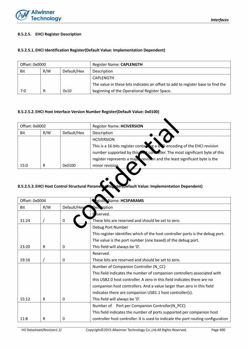
Interfaces
H3 Datasheet(Revision1.2) Copyright© 2015 Allwinner Technology Co.,Ltd.All Rights Reserved. Page 490
8.5.2.5. EHCI Register Description
8.5.2.5.1. EHCI Identification Register(Default Value: Implementation Dependent)
Offset: 0x0000 Register Name: CAPLENGTH
Bit R/W Default/Hex Description
7:0 R 0x10
CAPLENGTH
The value in these bits indicates an offset to add to register base to find the
beginning of the Operational Register Space.
8.5.2.5.2. EHCI Host Interface Version Number Register(Default Value: 0x0100)
Offset: 0x0002 Register Name: HCIVERSION
Bit R/W Default/Hex Description
15:0 R 0x0100
HCIVERSION
This is a 16-bits register containing a BCD encoding of the EHCI revision
number supported by this host controller. The most significant byte of this
register represents a major revision and the least significant byte is the
minor revision.
8.5.2.5.3. EHCI Host Control Structural Parameter Register(Default Value: Implementation Dependent)
Offset: 0x0004 Register Name: HCSPARAMS
Bit R/W Default/Hex Description
31:24 / 0
Reserved.
These bits are reserved and should be set to zero.
23:20 R 0
Debug Port Number
This register identifies which of the host controller ports is the debug port.
The value is the port number (one based) of the debug port.
This field will always be ‘0’.
19:16 / 0
Reserved.
These bits are reserved and should be set to zero.
15:12 R 0
Number of Companion Controller (N_CC)
This field indicates the number of companion controllers associated with
this USB2.0 host controller. A zero in this field indicates there are no
companion host controllers. And a value larger than zero in this field
indicates there are companion USB1.1 host controller(s).
This field will always be ‘0’.
11:8 R 0
Number of Port per Companion Controller(N_PCC)
This field indicates the number of ports supported per companion host
controller host controller. It is used to indicate the port routing configuration
confid
ential
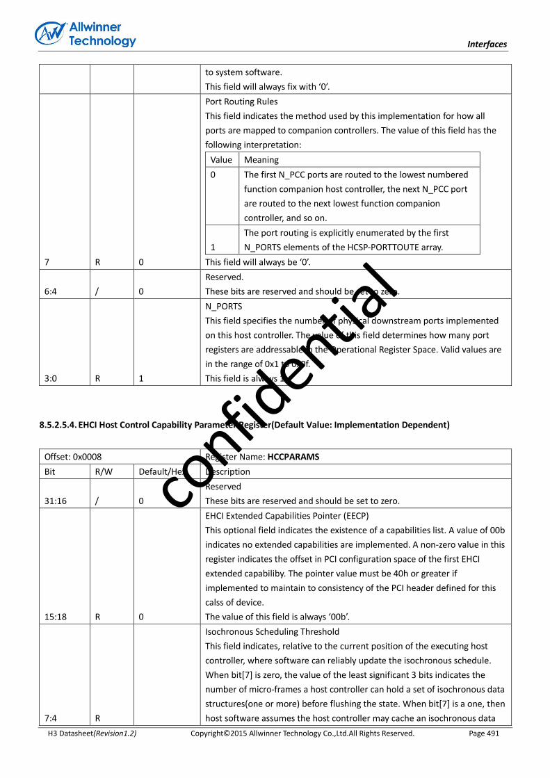
Interfaces
H3 Datasheet(Revision1.2) Copyright© 2015 Allwinner Technology Co.,Ltd.All Rights Reserved. Page 491
to system software.
This field will always fix with ‘0’.
7 R 0
Port Routing Rules
This field indicates the method used by this implementation for how all
ports are mapped to companion controllers. The value of this field has the
following interpretation:
Value Meaning
0 The first N_PCC ports are routed to the lowest numbered
function companion host controller, the next N_PCC port
are routed to the next lowest function companion
controller, and so on.
1
The port routing is explicitly enumerated by the first
N_PORTS elements of the HCSP-PORTTOUTE array.
This field will always be ‘0’.
6:4 / 0
Reserved.
These bits are reserved and should be set to zero.
3:0
R
1
N_PORTS
This field specifies the number of physical downstream ports implemented
on this host controller. The value of this field determines how many port
registers are addressable in the Operational Register Space. Valid values are
in the range of 0x1 to 0x0f.
This field is always 1.
8.5.2.5.4. EHCI Host Control Capability Parameter Register(Default Value: Implementation Dependent)
Offset: 0x0008 Register Name: HCCPARAMS
Bit R/W Default/Hex Description
31:16 / 0
Reserved
These bits are reserved and should be set to zero.
15:18 R 0
EHCI Extended Capabilities Pointer (EECP)
This optional field indicates the existence of a capabilities list. A value of 00b
indicates no extended capabilities are implemented. A non-zero value in this
register indicates the offset in PCI configuration space of the first EHCI
extended capabiliby. The pointer value must be 40h or greater if
implemented to maintain to consistency of the PCI header defined for this
calss of device.
The value of this field is always ‘00b’.
7:4 R
Isochronous Scheduling Threshold
This field indicates, relative to the current position of the executing host
controller, where software can reliably update the isochronous schedule.
When bit[7] is zero, the value of the least significant 3 bits indicates the
number of micro-frames a host controller can hold a set of isochronous data
structures(one or more) before flushing the state. When bit[7] is a one, then
host software assumes the host controller may cache an isochronous data
confid
ential
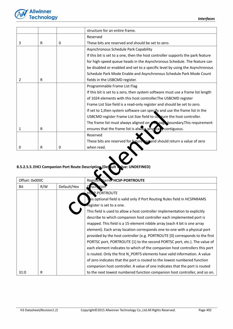
Interfaces
H3 Datasheet(Revision1.2) Copyright© 2015 Allwinner Technology Co.,Ltd.All Rights Reserved. Page 492
structure for an entire frame.
3 R 0
Reserved
These bits are reserved and should be set to zero.
2 R
Asynchronous Schedule Park Capability
If this bit is set to a one, then the host controller supports the park feature
for high-speed queue heads in the Asynchronous Schedule. The feature can
be disabled or enabled and set to a specific level by using the Asynchronous
Schedule Park Mode Enable and Asynchronous Schedule Park Mode Count
fields in the USBCMD register.
1 R
Programmable Frame List Flag
If this bit is set to a zero, then system software must use a frame list length
of 1024 elements with this host controller.The USBCMD register
Frame List Size field is a read-only register and should be set to zero.
If set to 1,then system software can specify and use the frame list in the
USBCMD register Frame List Size field to cofigure the host controller.
The frame list must always aligned on a 4K page boundary.This requirement
ensures that the frame list is always physically contiguous.
0 R 0
Reserved
These bits are reserved for future use and should return a value of zero
when read.
8.5.2.5.5. EHCI Companion Port Route Description (Default Value: UNDEFINED)
Offset: 0x000C Register Name: HCSP-PORTROUTE
Bit R/W Default/Hex Description
31:0 R
HCSP-PORTROUTE
This optional field is valid only if Port Routing Rules field in HCSPARAMS
register is set to a one.
This field is used to allow a host controller implementation to explicitly
describe to which companion host controller each implemented port is
mapped. This field is a 15-element nibble array (each 4 bit is one array
element). Each array location corresponds one-to-one with a physical port
provided by the host controller (e.g. PORTROUTE [0] corresponds to the first
PORTSC port, PORTROUTE [1] to the second PORTSC port, etc.). The value of
each element indicates to which of the companion host controllers this port
is routed. Only the first N_PORTS elements have valid information. A value
of zero indicates that the port is routed to the lowest numbered function
companion host controller. A value of one indicates that the port is routed
to the next lowest numbered function companion host controller, and so on.
confid
ential
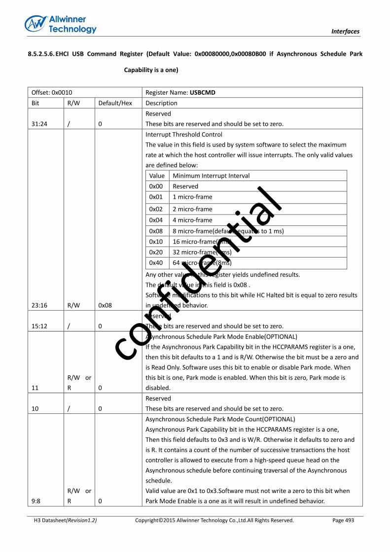
Interfaces
H3 Datasheet(Revision1.2) Copyright© 2015 Allwinner Technology Co.,Ltd.All Rights Reserved. Page 493
8.5.2.5.6. EHCI USB Command Register (Default Value: 0x00080000,0x00080B00 if Asynchronous Schedule Park
Capability is a one)
Offset: 0x0010 Register Name: USBCMD
Bit R/W Default/Hex Description
31:24 / 0
Reserved
These bits are reserved and should be set to zero.
23:16 R/W 0x08
Interrupt Threshold Control
The value in this field is used by system software to select the maximum
rate at which the host controller will issue interrupts. The only valid values
are defined below:
Value Minimum Interrupt Interval
0x00 Reserved
0x01 1 micro-frame
0x02 2 micro-frame
0x04 4 micro-frame
0x08 8 micro-frame(default, equates to 1 ms)
0x10 16 micro-frame(2ms)
0x20 32 micro-frame(4ms)
0x40 64 micro-frame(8ms)
Any other value in this register yields undefined results.
The default value in this field is 0x08 .
Software modifications to this bit while HC Halted bit is equal to zero results
in undefined behavior.
15:12 / 0
Reserved
These bits are reserved and should be set to zero.
11
R/W or
R 0
Asynchronous Schedule Park Mode Enable(OPTIONAL)
If the Asynchronous Park Capability bit in the HCCPARAMS register is a one,
then this bit defaults to a 1 and is R/W. Otherwise the bit must be a zero and
is Read Only. Software uses this bit to enable or disable Park mode. When
this bit is one, Park mode is enabled. When this bit is zero, Park mode is
disabled.
10 / 0
Reserved
These bits are reserved and should be set to zero.
9:8
R/W or
R 0
Asynchronous Schedule Park Mode Count(OPTIONAL)
Asynchronous Park Capability bit in the HCCPARAMS register is a one,
Then this field defaults to 0x3 and is W/R. Otherwise it defaults to zero and
is R. It contains a count of the number of successive transactions the host
controller is allowed to execute from a high-speed queue head on the
Asynchronous schedule before continuing traversal of the Asynchronous
schedule.
Valid value are 0x1 to 0x3.Software must not write a zero to this bit when
Park Mode Enable is a one as it will result in undefined behavior.
confid
ential
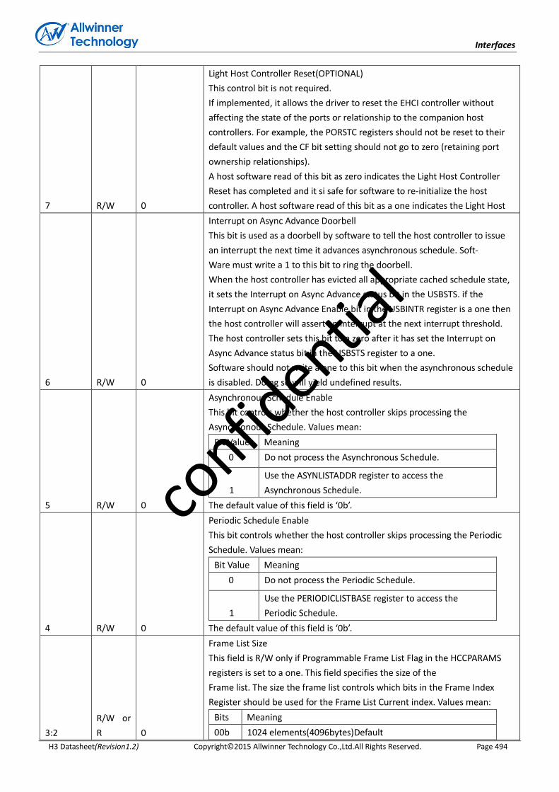
Interfaces
H3 Datasheet(Revision1.2) Copyright© 2015 Allwinner Technology Co.,Ltd.All Rights Reserved. Page 494
7 R/W 0
Light Host Controller Reset(OPTIONAL)
This control bit is not required.
If implemented, it allows the driver to reset the EHCI controller without
affecting the state of the ports or relationship to the companion host
controllers. For example, the PORSTC registers should not be reset to their
default values and the CF bit setting should not go to zero (retaining port
ownership relationships).
A host software read of this bit as zero indicates the Light Host Controller
Reset has completed and it si safe for software to re-initialize the host
controller. A host software read of this bit as a one indicates the Light Host
6 R/W 0
Interrupt on Async Advance Doorbell
This bit is used as a doorbell by software to tell the host controller to issue
an interrupt the next time it advances asynchronous schedule. Soft-
Ware must write a 1 to this bit to ring the doorbell.
When the host controller has evicted all appropriate cached schedule state,
it sets the Interrupt on Async Advance status bit in the USBSTS. if the
Interrupt on Async Advance Enable bit in the USBINTR register is a one then
the host controller will assert an interrupt at the next interrupt threshold.
The host controller sets this bit to a zero after it has set the Interrupt on
Async Advance status bit in the USBSTS register to a one.
Software should not write a one to this bit when the asynchronous schedule
is disabled. Doing so will yield undefined results.
5 R/W 0
Asynchronous Schedule Enable
This bit controls whether the host controller skips processing the
Asynchronous Schedule. Values mean:
Bit Value Meaning
0 Do not process the Asynchronous Schedule.
1
Use the ASYNLISTADDR register to access the
Asynchronous Schedule.
The default value of this field is ‘0b’.
4 R/W 0
Periodic Schedule Enable
This bit controls whether the host controller skips processing the Periodic
Schedule. Values mean:
Bit Value Meaning
0 Do not process the Periodic Schedule.
1
Use the PERIODICLISTBASE register to access the
Periodic Schedule.
The default value of this field is ‘0b’.
3:2
R/W or
R 0
Frame List Size
This field is R/W only if Programmable Frame List Flag in the HCCPARAMS
registers is set to a one. This field specifies the size of the
Frame list. The size the frame list controls which bits in the Frame Index
Register should be used for the Frame List Current index. Values mean:
Bits Meaning
00b 1024 elements(4096bytes)Default
confid
ential
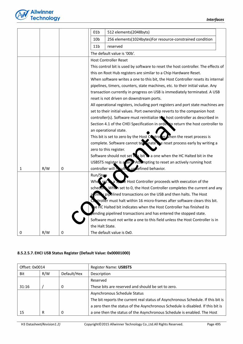
Interfaces
H3 Datasheet(Revision1.2) Copyright© 2015 Allwinner Technology Co.,Ltd.All Rights Reserved. Page 495
01b 512 elements(2048byts)
10b 256 elements(1024bytes)For resource-constrained condition
11b reserved
The default value is ‘00b’.
1 R/W 0
Host Controller Reset
This control bit is used by software to reset the host controller. The effects of
this on Root Hub registers are similar to a Chip Hardware Reset.
When software writes a one to this bit, the Host Controller resets its internal
pipelines, timers, counters, state machines, etc. to their initial value. Any
transaction currently in progress on USB is immediately terminated. A USB
reset is not driven on downstream ports.
All operational registers, including port registers and port state machines are
set to their initial values. Port ownership reverts to the companion host
controller(s). Software must reinitialize the host controller as described in
Section 4.1 of the CHEI Specification in order to return the host controller to
an operational state.
This bit is set to zero by the Host Controller when the reset process is
complete. Software cannot terminate the reset process early by writing a
zero to this register.
Software should not set this bit to a one when the HC Halted bit in the
USBSTS register is a zero. Attempting to reset an actively running host
controller will result in undefined behavior.
0 R/W 0
Run/Stop
When set to a 1, the Host Controller proceeds with execution of the
schedule. When set to 0, the Host Controller completes the current and any
actively pipelined transactions on the USB and then halts. The Host
Controller must halt within 16 micro-frames after software clears this bit.
The HC Halted bit indicates when the Host Controller has finished its
pending pipelined transactions and has entered the stopped state.
Software must not write a one to this field unless the Host Controller is in
the Halt State.
The default value is 0x0.
8.5.2.5.7. EHCI USB Status Register (Default Value: 0x00001000)
Offset: 0x0014 Register Name: USBSTS
Bit R/W Default/Hex Description
31:16 / 0
Reserved
These bits are reserved and should be set to zero.
15 R 0
Asynchronous Schedule Status
The bit reports the current real status of Asynchronous Schedule. If this bit is
a zero then the status of the Asynchronous Schedule is disabled. If this bit is
a one then the status of the Asynchronous Schedule is enabled. The Host
confid
ential
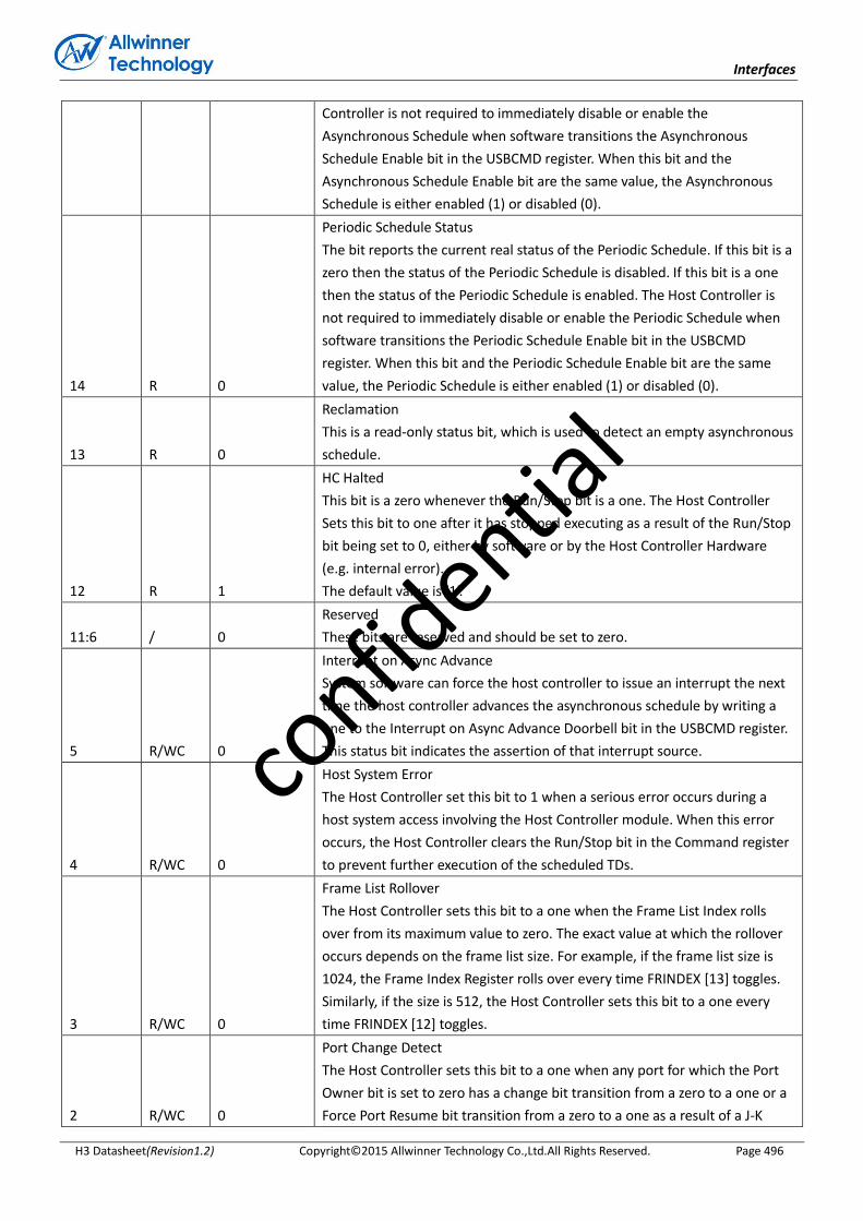
Interfaces
H3 Datasheet(Revision1.2) Copyright© 2015 Allwinner Technology Co.,Ltd.All Rights Reserved. Page 496
Controller is not required to immediately disable or enable the
Asynchronous Schedule when software transitions the Asynchronous
Schedule Enable bit in the USBCMD register. When this bit and the
Asynchronous Schedule Enable bit are the same value, the Asynchronous
Schedule is either enabled (1) or disabled (0).
14 R 0
Periodic Schedule Status
The bit reports the current real status of the Periodic Schedule. If this bit is a
zero then the status of the Periodic Schedule is disabled. If this bit is a one
then the status of the Periodic Schedule is enabled. The Host Controller is
not required to immediately disable or enable the Periodic Schedule when
software transitions the Periodic Schedule Enable bit in the USBCMD
register. When this bit and the Periodic Schedule Enable bit are the same
value, the Periodic Schedule is either enabled (1) or disabled (0).
13 R 0
Reclamation
This is a read-only status bit, which is used to detect an empty asynchronous
schedule.
12 R 1
HC Halted
This bit is a zero whenever the Run/Stop bit is a one. The Host Controller
Sets this bit to one after it has stopped executing as a result of the Run/Stop
bit being set to 0, either by software or by the Host Controller Hardware
(e.g. internal error).
The default value is ‘1’.
11:6 / 0
Reserved
These bits are reserved and should be set to zero.
5 R/WC 0
Interrupt on Async Advance
System software can force the host controller to issue an interrupt the next
time the host controller advances the asynchronous schedule by writing a
one to the Interrupt on Async Advance Doorbell bit in the USBCMD register.
This status bit indicates the assertion of that interrupt source.
4 R/WC 0
Host System Error
The Host Controller set this bit to 1 when a serious error occurs during a
host system access involving the Host Controller module. When this error
occurs, the Host Controller clears the Run/Stop bit in the Command register
to prevent further execution of the scheduled TDs.
3 R/WC 0
Frame List Rollover
The Host Controller sets this bit to a one when the Frame List Index rolls
over from its maximum value to zero. The exact value at which the rollover
occurs depends on the frame list size. For example, if the frame list size is
1024, the Frame Index Register rolls over every time FRINDEX [13] toggles.
Similarly, if the size is 512, the Host Controller sets this bit to a one every
time FRINDEX [12] toggles.
2 R/WC 0
Port Change Detect
The Host Controller sets this bit to a one when any port for which the Port
Owner bit is set to zero has a change bit transition from a zero to a one or a
Force Port Resume bit transition from a zero to a one as a result of a J-K
confid
ential

Interfaces
H3 Datasheet(Revision1.2) Copyright© 2015 Allwinner Technology Co.,Ltd.All Rights Reserved. Page 497
transition detected on a suspended port. This bit will also be set as a result
of the Connect Status Chang being set to a one after system software has
relinquished ownership of a connected port by writing a one to a port’s Port
Owner bit.
1 R/WC 0
USB Error Interrupt(USBERRINT)
The Host Controller sets this bit to 1 when completion of USB transaction
results in an error condition(e.g. error counter underflow).If the TD on
which the error interrupt occurred also had its IOC bit set, both.
This bit and USBINT bit are set.
0 R/WC 0
USB Interrupt(USBINT)
The Host Controller sets this bit to a one on the completion of a USB
transaction, which results in the retirement of a Transfer Descriptor that had
its IOC bit set.
The Host Controller also sets this bit to 1 when a short packet is detected
(actual number of bytes received was less than the expected number of
bytes)
8.5.2.5.8. EHCI USB Interrupt Enable Register (Default Value: 0x00000000)
Offset: 0x0018 Register Name: USBINTR
Bit R/W Default/Hex Description
31:6 / 0
Reserved
These bits are reserved and should be zero.
5 R/W 0
Interrupt on Async Advance Enable
When this bit is 1, and the Interrupt on Async Advance bit in the USBSTS
register is 1, the host controller will issue an interrupt at the next interrupt
threshold. The interrupt is acknowledged by software clearing the Interrupt
on Async Advance bit.
4 R/W 0
Host System Error Enable
When this bit is 1, and the Host System Error Status bit in the USBSTS
register is 1, the host controller will issue an interrupt. The interrupt is
acknowledged by software clearing the Host System Error bit.
3 R/W 0
Frame List Rollover Enable
When this bit is 1, and the Frame List Rollover bit in the USBSTS register is 1,
the host controller will issue an interrupt. The interrupt is acknowledged by
software clearing the Frame List Rollover bit.
2 R/W 0
Port Change Interrupt Enable
When this bit is 1, and the Port Chang Detect bit in the USBSTS register is 1,
the host controller will issue an interrupt. The interrupt is acknowledged by
software clearing the Port Chang Detect bit.
1 R/W 0
USB Error Interrupt Enable
When this bit is 1, and the USBERRINT bit in the USBSTS register is 1,the
host controller will issue an interrupt at the next interrupt threshold.
The interrupt is acknowledged by software clearing the USBERRINT bit.
confid
ential
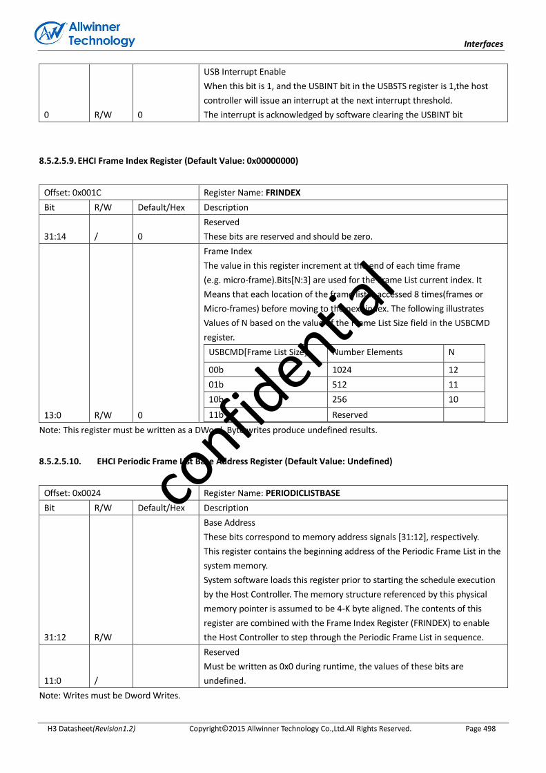
Interfaces
H3 Datasheet(Revision1.2) Copyright© 2015 Allwinner Technology Co.,Ltd.All Rights Reserved. Page 498
0 R/W 0
USB Interrupt Enable
When this bit is 1, and the USBINT bit in the USBSTS register is 1,the host
controller will issue an interrupt at the next interrupt threshold.
The interrupt is acknowledged by software clearing the USBINT bit
8.5.2.5.9. EHCI Frame Index Register (Default Value: 0x00000000)
Offset: 0x001C Register Name: FRINDEX
Bit R/W Default/Hex Description
31:14 / 0
Reserved
These bits are reserved and should be zero.
13:0 R/W 0
Frame Index
The value in this register increment at the end of each time frame
(e.g. micro-frame).Bits[N:3] are used for the Frame List current index. It
Means that each location of the frame list is accessed 8 times(frames or
Micro-frames) before moving to the next index. The following illustrates
Values of N based on the value of the Frame List Size field in the USBCMD
register.
USBCMD[Frame List Size] Number Elements N
00b 1024 12
01b 512 11
10b 256 10
11b Reserved
Note: This register must be written as a DWord. Byte writes produce undefined results.
8.5.2.5.10. EHCI Periodic Frame List Base Address Register (Default Value: Undefined)
Offset: 0x0024 Register Name: PERIODICLISTBASE
Bit R/W Default/Hex Description
31:12 R/W
Base Address
These bits correspond to memory address signals [31:12], respectively.
This register contains the beginning address of the Periodic Frame List in the
system memory.
System software loads this register prior to starting the schedule execution
by the Host Controller. The memory structure referenced by this physical
memory pointer is assumed to be 4-K byte aligned. The contents of this
register are combined with the Frame Index Register (FRINDEX) to enable
the Host Controller to step through the Periodic Frame List in sequence.
11:0 /
Reserved
Must be written as 0x0 during runtime, the values of these bits are
undefined.
Note: Writes must be Dword Writes.
confid
ential

Interfaces
H3 Datasheet(Revision1.2) Copyright© 2015 Allwinner Technology Co.,Ltd.All Rights Reserved. Page 499
8.5.2.5.11. EHCI Current Asynchronous List Address Register (Default Value: Undefined)
Offset: 0x0028 Register Name: ASYNCLISTADDR
Bit R/W Default/Hex Description
31:5 R/W
Link Pointer (LP)
This field contains the address of the next asynchronous queue head to be
executed.
These bits correspond to memory address signals [31:5], respectively.
4:0 / /
Reserved
These bits are reserved and their value has no effect on operation.
Bits in this field cannot be modified by system software and will always
return a zero when read.
Note: Write must be DWord Writes.
8.5.2.5.12. EHCI Configure Flag Register (Default Value: 0x00000000)
Offset: 0x0050 Register Name: CONFIGFLAG
Bit R/W Default/Hex Description
31:1 / 0
Reserved
These bits are reserved and should be set to zero.
0 R/W 0
Configure Flag(CF)
Host software sets this bit as the last action in its process of configuring the
Host Controller. This bit controls the default port-routing control logic as
follow:
Value Meaning
0 Port routing control logic default-routs each port to an
implementation dependent classic host controller.
1 Port routing control logic default-routs all ports to this host
controller.
The default value of this field is ‘0’.
Note: This register is not use in the normal implementation.
8.5.2.5.13. EHCI Port Status and Control Register (Default Value: 0x00002000(w/PPC set to one);0x00003000
(w/PPC set to a zero))
Offset: 0x0054 Register Name: PORTSC
Bit R/W Default/Hex Description
confid
ential
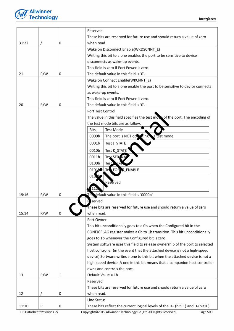
Interfaces
H3 Datasheet(Revision1.2) Copyright© 2015 Allwinner Technology Co.,Ltd.All Rights Reserved. Page 500
31:22 / 0
Reserved
These bits are reserved for future use and should return a value of zero
when read.
21 R/W 0
Wake on Disconnect Enable(WKDSCNNT_E)
Writing this bit to a one enables the port to be sensitive to device
disconnects as wake-up events.
This field is zero if Port Power is zero.
The default value in this field is ‘0’.
20 R/W 0
Wake on Connect Enable(WKCNNT_E)
Writing this bit to a one enable the port to be sensitive to device connects
as wake-up events.
This field is zero if Port Power is zero.
The default value in this field is ‘0’.
19:16 R/W 0
Port Test Control
The value in this field specifies the test mode of the port. The encoding of
the test mode bits are as follow:
Bits Test Mode
0000b The port is NOT operating in a test mode.
0001b Test J_STATE
0010b Test K_STATE
0011b Test SE0_NAK
0100b Test Packet
0101b Test FORCE_ENABLE
0110b
-
1111b
Reserved
The default value in this field is ‘0000b’.
15:14 R/W 0
Reserved
These bits are reserved for future use and should return a value of zero
when read.
13 R/W 1
Port Owner
This bit unconditionally goes to a 0b when the Configured bit in the
CONFIGFLAG register makes a 0b to 1b transition. This bit unconditionally
goes to 1b whenever the Configured bit is zero.
System software uses this field to release ownership of the port to selected
host controller (in the event that the attached device is not a high-speed
device).Software writes a one to this bit when the attached device is not a
high-speed device. A one in this bit means that a companion host controller
owns and controls the port.
Default Value = 1b.
12 / 0
Reserved
These bits are reserved for future use and should return a value of zero
when read.
11:10 R 0
Line Status
These bits reflect the current logical levels of the D+ (bit11) and D-(bit10)
confid
ential
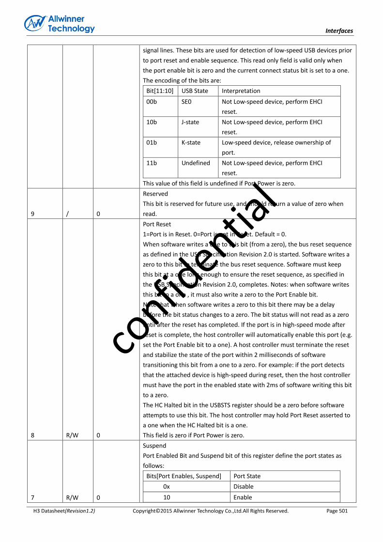
Interfaces
H3 Datasheet(Revision1.2) Copyright© 2015 Allwinner Technology Co.,Ltd.All Rights Reserved. Page 501
signal lines. These bits are used for detection of low-speed USB devices prior
to port reset and enable sequence. This read only field is valid only when
the port enable bit is zero and the current connect status bit is set to a one.
The encoding of the bits are:
Bit[11:10] USB State Interpretation
00b SE0 Not Low-speed device, perform EHCI
reset.
10b J-state Not Low-speed device, perform EHCI
reset.
01b K-state Low-speed device, release ownership of
port.
11b Undefined Not Low-speed device, perform EHCI
reset.
This value of this field is undefined if Port Power is zero.
9 / 0
Reserved
This bit is reserved for future use, and should return a value of zero when
read.
8 R/W 0
Port Reset
1=Port is in Reset. 0=Port is not in Reset. Default = 0.
When software writes a one to this bit (from a zero), the bus reset sequence
as defined in the USB Specification Revision 2.0 is started. Software writes a
zero to this bit to terminate the bus reset sequence. Software must keep
this bit at a one long enough to ensure the reset sequence, as specified in
the USB Specification Revision 2.0, completes. Notes: when software writes
this bit to a one , it must also write a zero to the Port Enable bit.
Note that when software writes a zero to this bit there may be a delay
before the bit status changes to a zero. The bit status will not read as a zero
until after the reset has completed. If the port is in high-speed mode after
reset is complete, the host controller will automatically enable this port (e.g.
set the Port Enable bit to a one). A host controller must terminate the reset
and stabilize the state of the port within 2 milliseconds of software
transitioning this bit from a one to a zero. For example: if the port detects
that the attached device is high-speed during reset, then the host controller
must have the port in the enabled state with 2ms of software writing this bit
to a zero.
The HC Halted bit in the USBSTS register should be a zero before software
attempts to use this bit. The host controller may hold Port Reset asserted to
a one when the HC Halted bit is a one.
This field is zero if Port Power is zero.
7 R/W 0
Suspend
Port Enabled Bit and Suspend bit of this register define the port states as
follows:
Bits[Port Enables, Suspend] Port State
0x Disable
10 Enable
confid
ential
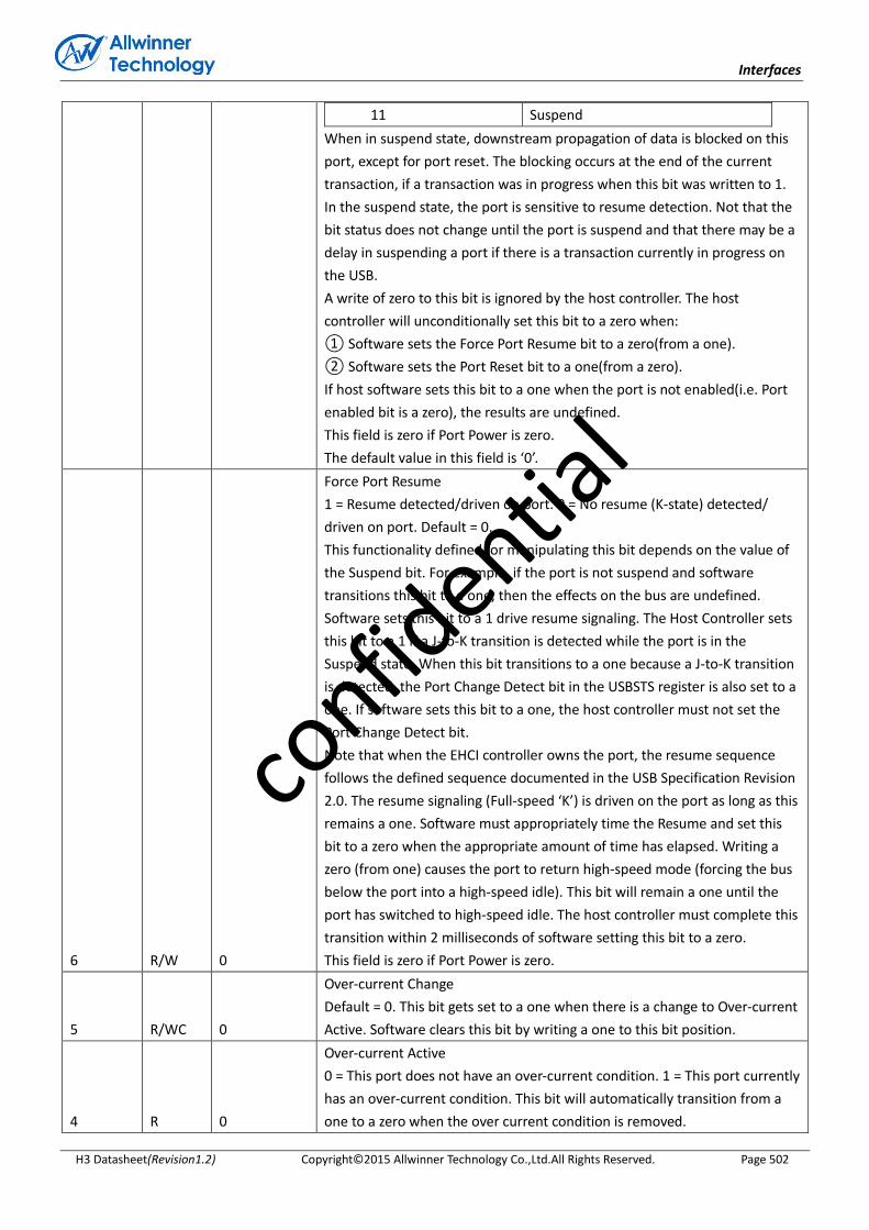
Interfaces
H3 Datasheet(Revision1.2) Copyright© 2015 Allwinner Technology Co.,Ltd.All Rights Reserved. Page 502
11 Suspend
When in suspend state, downstream propagation of data is blocked on this
port, except for port reset. The blocking occurs at the end of the current
transaction, if a transaction was in progress when this bit was written to 1.
In the suspend state, the port is sensitive to resume detection. Not that the
bit status does not change until the port is suspend and that there may be a
delay in suspending a port if there is a transaction currently in progress on
the USB.
A write of zero to this bit is ignored by the host controller. The host
controller will unconditionally set this bit to a zero when:
① Software sets the Force Port Resume bit to a zero(from a one).
② Software sets the Port Reset bit to a one(from a zero).
If host software sets this bit to a one when the port is not enabled(i.e. Port
enabled bit is a zero), the results are undefined.
This field is zero if Port Power is zero.
The default value in this field is ‘0’.
6 R/W 0
Force Port Resume
1 = Resume detected/driven on port. 0 = No resume (K-state) detected/
driven on port. Default = 0.
This functionality defined for manipulating this bit depends on the value of
the Suspend bit. For example, if the port is not suspend and software
transitions this bit to a one, then the effects on the bus are undefined.
Software sets this bit to a 1 drive resume signaling. The Host Controller sets
this bit to a 1 if a J-to-K transition is detected while the port is in the
Suspend state. When this bit transitions to a one because a J-to-K transition
is detected, the Port Change Detect bit in the USBSTS register is also set to a
one. If software sets this bit to a one, the host controller must not set the
Port Change Detect bit.
Note that when the EHCI controller owns the port, the resume sequence
follows the defined sequence documented in the USB Specification Revision
2.0. The resume signaling (Full-speed ‘K’) is driven on the port as long as this
remains a one. Software must appropriately time the Resume and set this
bit to a zero when the appropriate amount of time has elapsed. Writing a
zero (from one) causes the port to return high-speed mode (forcing the bus
below the port into a high-speed idle). This bit will remain a one until the
port has switched to high-speed idle. The host controller must complete this
transition within 2 milliseconds of software setting this bit to a zero.
This field is zero if Port Power is zero.
5 R/WC 0
Over-current Change
Default = 0. This bit gets set to a one when there is a change to Over-current
Active. Software clears this bit by writing a one to this bit position.
4 R 0
Over-current Active
0 = This port does not have an over-current condition. 1 = This port currently
has an over-current condition. This bit will automatically transition from a
one to a zero when the over current condition is removed.
confid
ential

Interfaces
H3 Datasheet(Revision1.2) Copyright© 2015 Allwinner Technology Co.,Ltd.All Rights Reserved. Page 503
The default value of this bit is ‘0’.
3 R/WC 0
Port Enable/Disable Change
Default = 0. 1 = Port enabled/disabled status has changed. 0 = No change.
For the root hub, this bit gets set to a one only when a port is disabled due
to the appropriate conditions existing at the EOF2 point (See Chapter 11 of
the USB Specification for the definition of a Port Error). Software clears this
bit by writing a 1 to it.
This field is zero if Port Power is zero.
2 R/W 0
Port Enabled/Disabled
1=Enable, 0=Disable. Ports can only be enabled by the host controller as a
part of the reset and enable. Software cannot enable a port by writing a one
to this field. The host controller will only set this bit to a one when the reset
sequence determines that the attached device is a high-speed device.
Ports can be disabled by either a fault condition(disconnect event or other
fault condition) or by host software. Note that the bit status does not
change until the port state actually changes. There may be a delay in
disabling or enabling a port due to other host controller and bus events.
When the port is disabled, downstream propagation of data is blocked on
this port except for reset.
The default value of this field is ‘0’.
This field is zero if Port Power is zero.
1 R/WC 0
Connect Status Change
1=Change in Current Connect Status, 0=No change, Default=0.
Indicates a change has occurred in the port’s Current Connect Status. The
host controller sets this bit for all changes to the port device connect status,
even if system software has not cleared an existing connect status change.
For example, the insertion status changes twice before system software has
cleared the changed condition, hub hardware will be “setting” an
already-set bit. Software sets this bit to 0 by writing a 1 to it.
This field is zero if Port Power is zero.
0 R 0
Current Connect Status
Device is present on port when the value of this field is a one, and no device
is present on port when the value of this field is a zero. This value reflects
the current state of the port, and may not correspond directly to the event
that caused the Connect Status Change(Bit 1) to be set.
This field is zero if Port Power zero.
Note: This register is only reset by hardware or in response to a host controller reset.
8.5.2.6. OHCI Register Description
confid
ential

Interfaces
H3 Datasheet(Revision1.2) Copyright© 2015 Allwinner Technology Co.,Ltd.All Rights Reserved. Page 504
8.5.2.6.1. HcRevision Register(Default Value: 0x00000010)
Offset: 0x400 Register Name: HcRevision
Bit
Read/Write
Default/Hex Description HCD HC
31:8 / / 0x00 Reserved
7:0 R R 0x10
Revision
This read-only field contains the BCD representation of the version of the
HCI specification that is implemented by this HC. For example, a value of
0x11 corresponds to version 1.1. All of the HC implementations that are
compliant with this specification will have a value of 0x10.
8.5.2.6.2. HcControl Register(Default Value: 0x00000000)
Offset: 0x404 Register Name: HcRevision
Bit
Read/Write
Default/Hex
Description HCD HC
31:11 / / 0x00 Reserved
10 R/W R 0x0
RemoteWakeupEnable
This bit is used by HCD to enable or disable the remote wakeup feature
upon the detection of upstream resume signaling. When this bit is set and
the ResumeDetected bit in HcInterruptStatus is set, a remote wakeup is
signaled to the host system. Setting this bit has no impact on the
generation of hardware interrupt.
9 R/W R/W 0x0
RemoteWakeupConnected
This bit indicates whether HC supports remote wakeup signaling. If remote
wakeup is supported and used by the system, it is the responsibility of
system firmware to set this bit during POST. HC clear the bit upon a
hardware reset but does not alter it upon a software reset. Remote wakeup
signaling of the host system is host-bus-specific and is not described in this
specification.
8 R/W R 0x0
InterruptRouting
This bit determines the routing of interrupts generated by events registered
in HcInterruptStatus. If clear, all interrupt are routed to the normal host bus
interrupt mechanism. If set interrupts are routed to the System
Management Interrupt. HCD clears this bit upon a hardware reset, but it
does not alter this bit upon a software reset. HCD uses this bit as a tag to
indicate the ownership of HC.
7:6 R/W R/W 0x0
HostControllerFunctionalState for USB
00b USBReset
01b USBResume
10b USBOperational
confid
ential

Interfaces
H3 Datasheet(Revision1.2) Copyright© 2015 Allwinner Technology Co.,Ltd.All Rights Reserved. Page 505
11b USBSuspend
A transition to USBOperational from another state causes SOF generation
to begin 1 ms later. HCD may determine whether HC has begun sending
SOFs by reading the StartoFrame field of
HcInterruptStatus.
This field may be changed by HC only when in the USBSUSPEND state. HC
may move from the USBSUSPEND state to the USBRESUME state after
detecting the resume signaling from a downstream port.
HC enters USBSUSPEND after a software reset, whereas it enters
USBRESET after a hardware reset. The latter also resets the Root
Hub and asserts subsequent reset signaling to downstream ports.
5 R/W R 0x0
BulkListEnable
This bit is set to enable the processing of the Bulk list in the next
Frame. If cleared by HCD, processing of the Bulk list does not occur after
the next SOF. HC checks this bit whenever it determines to process the list.
When disabled, HCD may modify the list. If HcBulkCurrentED is pointing to
an ED to be removed, HCD must advance the pointer by updating
HcBulkCurrentED before re-enabling processing of the list.
4 R/W R 0x0
ControlListEnable
This bit is set to enable the processing of the Control list in the next Frame.
If cleared by HCD, processing of the Control list does not occur after the
next SOF. HC must check this bit whenever it determines to process the list.
When disabled, HCD may modify the list. If HcControlCurrentED is pointing
to an ED to be removed, HCD must advance the pointer by updating
HcControlCurrentED before re-enabling processing of the list.
3 R/W R 0x0
IsochronousEnable
This bit is used by HCD to enable/disable processing of isochronous EDs.
While processing the periodic list in a Frame, HC checks the status of this
bit when it finds an Isochronous ED (F=1). If set (enabled), HC continues
processing the EDs. If cleared (disabled), HC halts processing of the periodic
list (which now contains only isochronous EDs) and begins processing the
Bulk/Control lists.
Setting this bit is guaranteed to take effect in the next Frame (not the
current Frame).
2 R/W R 0x0
PeriodicListEnable
This bit is set to enable the processing of periodic list in the next Frame. If
cleared by HCD, processing of the periodic list does not occur after the next
SOF. HC must check this bit before it starts processing the list.
1:0 R/W R 0x0
ControlBulkServiceRatio
This specifies the service ratio between Control and Bulk EDs. Before
processing any of the nonperiodic lists, HC must compare the ratio
specified with its internal count on how many nonempty Control EDs have
been processed, in determining whether to continue serving another
Control ED or switching to Bulk EDs. The internal count will be retained
when crossing the frame boundary. In case of reset, HCD is responsible for
confid
ential

Interfaces
H3 Datasheet(Revision1.2) Copyright© 2015 Allwinner Technology Co.,Ltd.All Rights Reserved. Page 506
restoring this value.
CBSR No. of Control EDs Over Bulk EDs Served
0 1:1
1 2:1
2 3:1
3 4:1
The default value is 0x0.
8.5.2.6.3. HcCommandStatus Register(Default Value: 0x00000000)
Offset: 0x408 Register Name: HcCommandStatus
Bit
Read/Write
Default/Hex Description HCD HC
31:18 / / 0x0 Reserved
17:16 R R/W 0x0
SchedulingOverrunCount
These bits are incremented on each scheduling overrun error. It is initialized
to 00b and wraps around at 11b. This will be incremented when a
scheduling overrun is detected even if SchedulingOverrun in
HcInterruptStatus has already been set. This is used by HCD to monitor any
persistent scheduling problem.
15:4 / / 0x0 Reserved
3 R/W R/W 0x0
OwershipChangeRequest
This bit is set by an OS HCD to request a change of control of the HC. When
set HC will set the OwnershipChange field in HcInterruptStatus. After the
changeover, this bit is cleared and remains so until the next request from
OS HCD.
2 R/W R/W 0x0
BulklListFilled
This bit is used to indicate whether there are any TDs on the Bulk list. It is
set by HCD whenever it adds a TD to an ED in the Bulk list.
When HC begins to process the head of the Bulk list, it checks BLF. As long
as BulkListFilled is 0, HC will not start processing the Bulk list. If
BulkListFilled is 1, HC will start processing the Bulk list and will set BF to 0. If
HC finds a TD on the list, then HC will set BulkListFilled to 1 causing the Bulk
list processing to continue. If no TD is found on the Bulk list, and if HCD
does not set BulkListFilled, then BulkListFilled will still be 0 when HC
completes processing the Bulk list and Bulk list processing will stop.
1 R/W R/W 0x0
ControlListFilled
This bit is used to indicate whether there are any TDs on the Control list. It
is set by HCD whenever it adds a TD to an ED in the Control list.
When HC begins to process the head of the Control list, it checks CLF. As
long as ControlListFilled is 0, HC will not start processing the Control list. If
CF is 1, HC will start processing the Control list and will set ControlListFilled
to 0. If HC finds a TD on the list, then HC will set ControlListFilled to 1
confid
ential
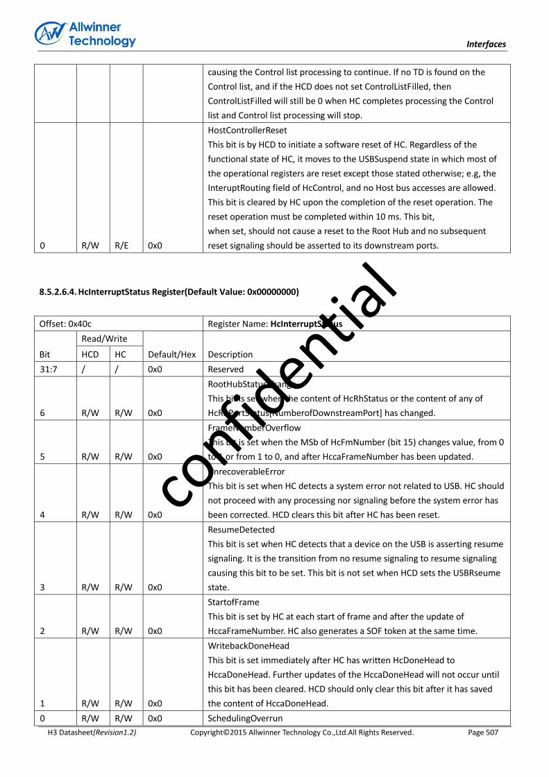
Interfaces
H3 Datasheet(Revision1.2) Copyright© 2015 Allwinner Technology Co.,Ltd.All Rights Reserved. Page 507
causing the Control list processing to continue. If no TD is found on the
Control list, and if the HCD does not set ControlListFilled, then
ControlListFilled will still be 0 when HC completes processing the Control
list and Control list processing will stop.
0 R/W R/E 0x0
HostControllerReset
This bit is by HCD to initiate a software reset of HC. Regardless of the
functional state of HC, it moves to the USBSuspend state in which most of
the operational registers are reset except those stated otherwise; e.g, the
InteruptRouting field of HcControl, and no Host bus accesses are allowed.
This bit is cleared by HC upon the completion of the reset operation. The
reset operation must be completed within 10 ms. This bit,
when set, should not cause a reset to the Root Hub and no subsequent
reset signaling should be asserted to its downstream ports.
8.5.2.6.4. HcInterruptStatus Register(Default Value: 0x00000000)
Offset: 0x40c Register Name: HcInterruptStatus
Bit
Read/Write
Default/Hex Description HCD HC
31:7 / / 0x0 Reserved
6 R/W R/W 0x0
RootHubStatusChange
This bit is set when the content of HcRhStatus or the content of any of
HcRhPortStatus[NumberofDownstreamPort] has changed.
5 R/W R/W 0x0
FrameNumberOverflow
This bit is set when the MSb of HcFmNumber (bit 15) changes value, from 0
to 1 or from 1 to 0, and after HccaFrameNumber has been updated.
4 R/W R/W 0x0
UnrecoverableError
This bit is set when HC detects a system error not related to USB. HC should
not proceed with any processing nor signaling before the system error has
been corrected. HCD clears this bit after HC has been reset.
3 R/W R/W 0x0
ResumeDetected
This bit is set when HC detects that a device on the USB is asserting resume
signaling. It is the transition from no resume signaling to resume signaling
causing this bit to be set. This bit is not set when HCD sets the USBRseume
state.
2 R/W R/W 0x0
StartofFrame
This bit is set by HC at each start of frame and after the update of
HccaFrameNumber. HC also generates a SOF token at the same time.
1 R/W R/W 0x0
WritebackDoneHead
This bit is set immediately after HC has written HcDoneHead to
HccaDoneHead. Further updates of the HccaDoneHead will not occur until
this bit has been cleared. HCD should only clear this bit after it has saved
the content of HccaDoneHead.
0 R/W R/W 0x0 SchedulingOverrun
confid
ential

Interfaces
H3 Datasheet(Revision1.2) Copyright© 2015 Allwinner Technology Co.,Ltd.All Rights Reserved. Page 508
This bit is set when the USB schedule for the current Frame overruns and
after the update of HccaFrameNumber. A scheduling overrun will also
cause the SchedulingOverrunCount of HcCommandStatus to be
Incremented.
8.5.2.6.5. HcInterruptEnable Register(Default Value: 0x00000000)
Offset: 0x410 Register Name: HcInterruptEnable Register
Bit
Read/Write
Default/Hex Description HCD HC
31 R/W R 0x0
MasterInterruptEnable
A ‘0’ writtern to this field is ignored by HC. A ‘1’ written to this field enables
interrupt generation due to events specified in the other bits of this
register. This is used by HCD as Master Interrupt Enable.
30:7 / / 0x0 Reserved
6 R/W R 0x0
RootHubStatusChange Interrupt Enable
0 Ignore;
1 Enable interrupt generation due to Root Hub Status Change;
5 R/W R 0x0
FrameNumberOverflow Interrupt Enable
0 Ignore;
1 Enable interrupt generation due to Frame Number Over Flow;
4 R/W R 0x0
UnrecoverableError Interrupt Enable
0 Ignore;
1 Enable interrupt generation due to Unrecoverable Error;
3 R/W R 0x0
ResumeDetected Interrupt Enable
0 Ignore;
1 Enable interrupt generation due to Resume Detected;
2 R/W R 0x0
StartofFrame Interrupt Enable
0 Ignore;
1 Enable interrupt generation due to Start of Flame;
1 R/W R 0x0
WritebackDoneHead Interrupt Enable
0 Ignore;
1 Enable interrupt generation due to Write back Done Head;
0 R/W R 0x0
SchedulingOverrun Interrupt Enable
0 Ignore;
1 Enable interrupt generation due to Scheduling Overrun;
8.5.2.6.6. HcInterruptDisable Register(Default Value: 0x00000000)
Offset: 0x414 Register Name: HcInterruptDisable Register
confid
ential

Interfaces
H3 Datasheet(Revision1.2) Copyright© 2015 Allwinner Technology Co.,Ltd.All Rights Reserved. Page 509
Bit
Read/Write
Default/Hex Description HCD HC
31 R/W R 0x0
MasterInterruptEnable
A written ‘0’ to this field is ignored by HC. A ‘1’ written to this field disables
interrupt generation due events specified in the other bits of this register.
This field is set after a hardware or software reset.
30:7 / / 0x00 Reserved
6 R/W R 0x0
RootHubStatusChange Interrupt Disable
0 Ignore;
1 Disable interrupt generation due to Root Hub Status Change;
5 R/W R 0x0
FrameNumberOverflow Interrupt Disable
0 Ignore;
1 Disable interrupt generation due to Frame Number Over Flow;
4 R/W R 0x0
UnrecoverableError Interrupt Disable
0 Ignore;
1 Disable interrupt generation due to Unrecoverable Error;
3 R/W R 0x0
ResumeDetected Interrupt Disable
0 Ignore;
1 Disable interrupt generation due to Resume Detected;
2 R/W R 0x0
StartofFrame Interrupt Disable
0 Ignore;
1 Disable interrupt generation due to Start of Flame;
1 R/W R 0x0
WritebackDoneHead Interrupt Disable
0 Ignore;
1 Disable interrupt generation due to Write back Done Head;
0 R/w R 0x0
SchedulingOverrun Interrupt Disable
0 Ignore;
1 Disable interrupt generation due to Scheduling Overrun;
8.5.2.6.7. HcHCCA Register(Default Value: 0x00000000)
Offset: 0x418 Register Name: HcHCCA
Bit
Read/Write
Default/Hex Description HCD HC
31:8 R/W R 0x0
HCCA[31:8]
This is the base address of the Host Controller Communication Area. This
area is used to hold the control structures and the Interrupt table that are
accessed by both the Host Controller and the Host Controller Driver.
7:0 R R 0x0
HCCA[7:0]
The alignment restriction in HcHCCA register is evaluated by examining the
number of zeros in the lower order bits. The minimum alignment is 256
bytes, therefore, bits 0 through 7 must always return 0 when read.
confid
ential
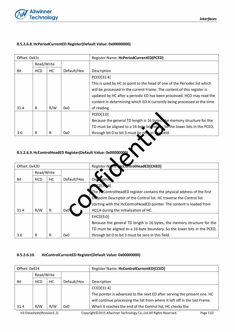
Interfaces
H3 Datasheet(Revision1.2) Copyright© 2015 Allwinner Technology Co.,Ltd.All Rights Reserved. Page 510
8.5.2.6.8. HcPeriodCurrentED Register(Default Value: 0x00000000)
Offset: 0x41c Register Name: HcPeriodCurrentED(PCED)
Bit
Read/Write
Default/Hex Description HCD HC
31:4 R R/W 0x0
PCED[31:4]
This is used by HC to point to the head of one of the Periodec list which
will be processed in the current Frame. The content of this register is
updated by HC after a periodic ED has been processed. HCD may read the
content in determining which ED is currently being processed at the time
of reading.
3:0 R R 0x0
PCED[3:0]
Because the general TD length is 16 bytes, the memory structure for the
TD must be aligned to a 16-byte boundary. So the lower bits in the PCED,
through bit 0 to bit 3 must be zero in this field.
8.5.2.6.9. HcControlHeadED Register(Default Value: 0x00000000)
Offset: 0x420 Register Name: HcControlHeadED[CHED]
Bit
Read/Write
Default/Hex Description HCD HC
31:4 R/W R 0x0
EHCD[31:4]
The HcControlHeadED register contains the physical address of the first
Endpoint Descriptor of the Control list. HC traverse the Control list
starting with the HcControlHeadED pointer. The content is loaded from
HCCA during the initialization of HC.
3:0 R R 0x0
EHCD[3:0]
Because the general TD length is 16 bytes, the memory structure for the
TD must be aligned to a 16-byte boundary. So the lower bits in the PCED,
through bit 0 to bit 3 must be zero in this field.
8.5.2.6.10. HcControlCurrentED Register(Default Value: 0x00000000)
Offset: 0x424 Register Name: HcControlCurrentED[CCED]
Bit
Read/Write
Default/Hex Description HCD HC
31:4 R/W R/W 0x0
CCED[31:4]
The pointer is advanced to the next ED after serving the present one. HC
will continue processing the list from where it left off in the last Frame.
When it reaches the end of the Control list, HC checks the
confid
ential

Interfaces
H3 Datasheet(Revision1.2) Copyright© 2015 Allwinner Technology Co.,Ltd.All Rights Reserved. Page 511
ControlListFilled of in HcCommandStatus. If set, it copies the content of
HcControlHeadED to HcControlCurrentED and clears the bit. If not set, it
does nothing.
HCD is allowed to modify this register only when the ControlListEnable of
HcControl is cleared. When set, HCD only reads the instantaneous value
of this register. Initially, this is set to zero to indicate the end of the
Control list.
3:0 R R 0x0
CCED[3:0]
Because the general TD length is 16 bytes, the memory structure for the
TD must be aligned to a 16-byte boundary. So the lower bits in the PCED,
through bit 0 to bit 3 must be zero in this field.
8.5.2.6.11. HcBulkHeadED Register(Default Value: 0x00000000)
Offset: 0x428 Register Name: HcBulkHeadED[BHED]
Bit
Read/Write
Default/Hex Description HCD HC
31:4 R/W R 0x0
BHED[31:4]
The HcBulkHeadED register contains the physical address of the first
Endpoint Descriptor of the Bulk list. HC traverses the Bulk list starting with
the HcBulkHeadED pointer. The content is loaded from HCCA during the
initialization of HC.
3:0 R R 0x0
BHED[3:0]
Because the general TD length is 16 bytes, the memory structure for the
TD must be aligned to a 16-byte boundary. So the lower bits in the PCED,
through bit 0 to bit 3 must be zero in this field.
8.5.2.6.12. HcBulkCurrentED Register(Default Value: 0x00000000)
Offset: 0x42c Register Name: HcBulkCurrentED [BCED]
Bit
Read/Write
Default/Hex Description HCD HC
31:4 R/W R/W 0x0
BulkCurrentED[31:4]
This is advanced to the next ED after the HC has served the present one.
HC continues processing the list from where it left off in the last Frame.
When it reaches the end of the Bulk list, HC checks the ControlListFilled of
HcControl. If set, it copies the content of HcBulkHeadED to
HcBulkCurrentED and clears the bit. If it is not set, it does nothing. HCD is
only allowed to modify this register when the BulkListEnable of HcControl
is cleared. When set, the HCD only reads the instantaneous value of this
register. This is initially set to zero to indicate the end of the Bulk list.
3:0 R R 0x0 BulkCurrentED [3:0]
confid
ential

Interfaces
H3 Datasheet(Revision1.2) Copyright© 2015 Allwinner Technology Co.,Ltd.All Rights Reserved. Page 512
Because the general TD length is 16 bytes, the memory structure for the
TD must be aligned to a 16-byte boundary. So the lower bits in the PCED,
through bit 0 to bit 3 must be zero in this field.
8.5.2.6.13. HcDoneHead Register(Default Value: 0x00000000)
Offset: 0x430 Register Name: HcDoneHead
Bit
Read/Write
Default/Hex Description HCD HC
31:4 R R/W 0x0
HcDoneHead[31:4]
When a TD is completed, HC writes the content of HcDoneHead to the
NextTD field of the TD. HC then overwrites the content of HcDoneHead
with the address of this TD. This is set to zero whenever HC writes the
content of this register to HCCA. It also sets the WritebackDoneHead of
HcInterruptStatus.
3:0 R R 0x0
HcDoneHead[3:0]
Because the general TD length is 16 bytes, the memory structure for the
TD must be aligned to a 16-byte boundary. So the lower bits in the PCED,
through bit 0 to bit 3 must be zero in this field.
8.5.2.6.14. HcFmInterval Register(Default Value: 0x00002EDF)
Offset: 0x434 Register Name: HcFmInterval Register
Bit
Read/Write
Default/Hex Description HCD HC
31 R/W R 0x0
FrameIntervalToggler
HCD toggles this bit whenever it loads a new value to FrameInterval.
30:16 R/W R 0x0
FSLargestDataPacket
This field specifies a value which is loaded into the Largest Data Packet
Counter at the beginning of each frame. The counter value represents the
largest amount of data in bits which can be sent or received by the HC in a
single transaction at any given time without causing scheduling overrun.
The field value is calculated by the HCD.
15:14 / / 0x0 Reserved
13:0 R/W R 0x2edf
FrameInterval
This specifies the interval between two consecutive SOFs in bit times. The
nominal value is set to be 11,999. HCD should store the current value of
this field before resetting HC. By setting the HostControllerReset field of
HcCommandStatus as this will cause the HC to reset this field to its
nominal value. HCD may choose to restore the stored value upon the
completion of the Reset sequence.
confid
ential
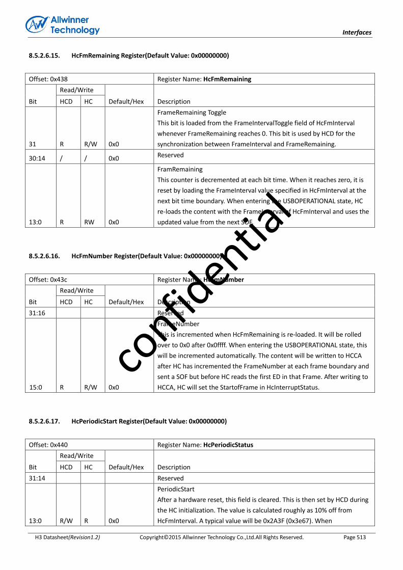
Interfaces
H3 Datasheet(Revision1.2) Copyright© 2015 Allwinner Technology Co.,Ltd.All Rights Reserved. Page 513
8.5.2.6.15. HcFmRemaining Register(Default Value: 0x00000000)
Offset: 0x438 Register Name: HcFmRemaining
Bit
Read/Write
Default/Hex Description HCD HC
31 R R/W 0x0
FrameRemaining Toggle
This bit is loaded from the FrameIntervalToggle field of HcFmInterval
whenever FrameRemaining reaches 0. This bit is used by HCD for the
synchronization between FrameInterval and FrameRemaining.
30:14 / / 0x0 Reserved
13:0 R RW 0x0
FramRemaining
This counter is decremented at each bit time. When it reaches zero, it is
reset by loading the FrameInterval value specified in HcFmInterval at the
next bit time boundary. When entering the USBOPERATIONAL state, HC
re-loads the content with the FrameInterval of HcFmInterval and uses the
updated value from the next SOF.
8.5.2.6.16. HcFmNumber Register(Default Value: 0x00000000)
Offset: 0x43c Register Name: HcFmNumber
Bit
Read/Write
Default/Hex Description HCD HC
31:16 Reserved
15:0 R R/W 0x0
FrameNumber
This is incremented when HcFmRemaining is re-loaded. It will be rolled
over to 0x0 after 0x0ffff. When entering the USBOPERATIONAL state, this
will be incremented automatically. The content will be written to HCCA
after HC has incremented the FrameNumber at each frame boundary and
sent a SOF but before HC reads the first ED in that Frame. After writing to
HCCA, HC will set the StartofFrame in HcInterruptStatus.
8.5.2.6.17. HcPeriodicStart Register(Default Value: 0x00000000)
Offset: 0x440 Register Name: HcPeriodicStatus
Bit
Read/Write
Default/Hex Description HCD HC
31:14 Reserved
13:0 R/W R 0x0
PeriodicStart
After a hardware reset, this field is cleared. This is then set by HCD during
the HC initialization. The value is calculated roughly as 10% off from
HcFmInterval. A typical value will be 0x2A3F (0x3e67). When
confid
ential
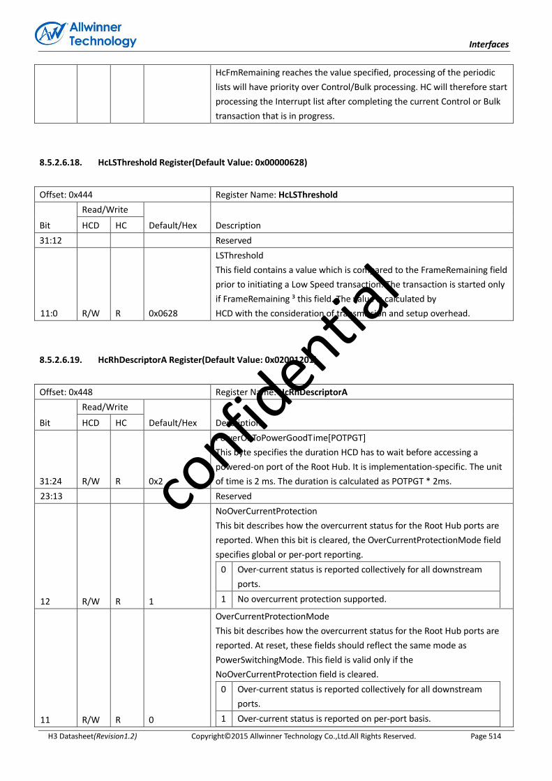
Interfaces
H3 Datasheet(Revision1.2) Copyright© 2015 Allwinner Technology Co.,Ltd.All Rights Reserved. Page 514
HcFmRemaining reaches the value specified, processing of the periodic
lists will have priority over Control/Bulk processing. HC will therefore start
processing the Interrupt list after completing the current Control or Bulk
transaction that is in progress.
8.5.2.6.18. HcLSThreshold Register(Default Value: 0x00000628)
Offset: 0x444 Register Name: HcLSThreshold
Bit
Read/Write
Default/Hex Description HCD HC
31:12 Reserved
11:0 R/W R 0x0628
LSThreshold
This field contains a value which is compared to the FrameRemaining field
prior to initiating a Low Speed transaction. The transaction is started only
if FrameRemaining ³ this field. The value is calculated by
HCD with the consideration of transmission and setup overhead.
8.5.2.6.19. HcRhDescriptorA Register(Default Value: 0x02001201)
Offset: 0x448 Register Name: HcRhDescriptorA
Bit
Read/Write
Default/Hex Description HCD HC
31:24 R/W R 0x2
PowerOnToPowerGoodTime[POTPGT]
This byte specifies the duration HCD has to wait before accessing a
powered-on port of the Root Hub. It is implementation-specific. The unit
of time is 2 ms. The duration is calculated as POTPGT * 2ms.
23:13 Reserved
12 R/W R 1
NoOverCurrentProtection
This bit describes how the overcurrent status for the Root Hub ports are
reported. When this bit is cleared, the OverCurrentProtectionMode field
specifies global or per-port reporting.
0 Over-current status is reported collectively for all downstream
ports.
1 No overcurrent protection supported.
11 R/W R 0
OverCurrentProtectionMode
This bit describes how the overcurrent status for the Root Hub ports are
reported. At reset, these fields should reflect the same mode as
PowerSwitchingMode. This field is valid only if the
NoOverCurrentProtection field is cleared.
0 Over-current status is reported collectively for all downstream
ports.
1 Over-current status is reported on per-port basis.
confid
ential

Interfaces
H3 Datasheet(Revision1.2) Copyright© 2015 Allwinner Technology Co.,Ltd.All Rights Reserved. Page 515
10 R R 0x0
Device Type
This bit specifies that the Root Hub is not a compound device. The Root
Hub is not permitted to be a compound device. This field should always
read/write 0.
9 R/W R 1
PowerSwitchingMode
This bit is used to specify how the power switching of the Root Hub ports
is controlled. It is implementation-specific. This field is only valid if the
NoPowerSwitching field is cleared.
0 All ports are powered at the same time.
1 Each port is powered individually. This mode allows port power
to be controlled by either the global switch or per-port
switching. If the PortPowerControlMask bit is set, the port
responds only to port power commands (Set/ClearPortPower).
If the port mask is cleared, then the port is controlled only by
the global power switch (Set/ClearGlobalPower).
8 R/W R 0
NoPowerSwithcing
These bits are used to specify whether power switching is supported or
ports are always powered. It is implementation-specific. When this bit is
cleared, the PowerSwitchingMode specifies global or per-port switching.
0 Ports are power switched.
1 Ports are always powered on when the HC is powered on.
7:0 R R 0x01
NumberDownstreamPorts
These bits specify the number of downstream ports supported by the
Root Hub. It is implementation-specific. The minimum number of ports is
1. The maximum number of ports supported.
8.5.2.6.20. HcRhDescriptorB Register(Default Value: 0x00000000)
Offset: 0x44c Register Name: HcRhDescriptorB Register
Bit
Read/Write
Default/Hex Description HCD HC
31:16 R/W R 0x0
PortPowerControlMask
Each bit indicates if a port is affected by a global power control command
when PowerSwitchingMode is set. When set, the port's power state is
only affected by per-port power control (Set/ClearPortPower). When
cleared, the port is controlled by the global power switch
(Set/ClearGlobalPower). If the device is configured to global switching
mode (PowerSwitchingMode = 0 ), this field is not valid.
Bit0 Reserved
Bit1 Ganged-power mask on Port #1.
Bit2 Ganged-power mask on Port #2.
confid
ential
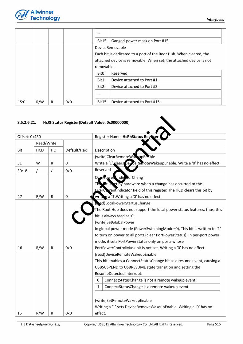
Interfaces
H3 Datasheet(Revision1.2) Copyright© 2015 Allwinner Technology Co.,Ltd.All Rights Reserved. Page 516
…
Bit15 Ganged-power mask on Port #15.
15:0 R/W R 0x0
DeviceRemovable
Each bit is dedicated to a port of the Root Hub. When cleared, the
attached device is removable. When set, the attached device is not
removable.
Bit0 Reserved
Bit1 Device attached to Port #1.
Bit2 Device attached to Port #2.
…
Bit15 Device attached to Port #15.
8.5.2.6.21. HcRhStatus Register(Default Value: 0x00000000)
Offset: 0x450 Register Name: HcRhStatus Register
Bit
Read/Write
Default/Hex Description HCD HC
31 W R 0
(write)ClearRemoteWakeupEnable
Write a ‘1’ clears DeviceRemoteWakeupEnable. Write a ‘0’ has no effect.
30:18 / / 0x0 Reserved
17 R/W R 0
OverCurrentIndicatorChang
This bit is set by hardware when a change has occurred to the
OverCurrentIndicator field of this register. The HCD clears this bit by
writing a ‘1’.Writing a ‘0’ has no effect.
16 R/W R 0x0
(read)LocalPowerStartusChange
The Root Hub does not support the local power status features, thus, this
bit is always read as ‘0’.
(write)SetGlobalPower
In global power mode (PowerSwitchingMode=0), This bit is written to ‘1’
to turn on power to all ports (clear PortPowerStatus). In per-port power
mode, it sets PortPowerStatus only on ports whose
PortPowerControlMask bit is not set. Writing a ‘0’ has no effect.
15 R/W R 0x0
(read)DeviceRemoteWakeupEnable
This bit enables a ConnectStatusChange bit as a resume event, causing a
USBSUSPEND to USBRESUME state transition and setting the
ResumeDetected interrupt.
0 ConnectStatusChange is not a remote wakeup event.
1 ConnectStatusChange is a remote wakeup event.
(write)SetRemoteWakeupEnable
Writing a ‘1’ sets DeviceRemoveWakeupEnable. Writing a ‘0’ has no
effect.
confid
ential
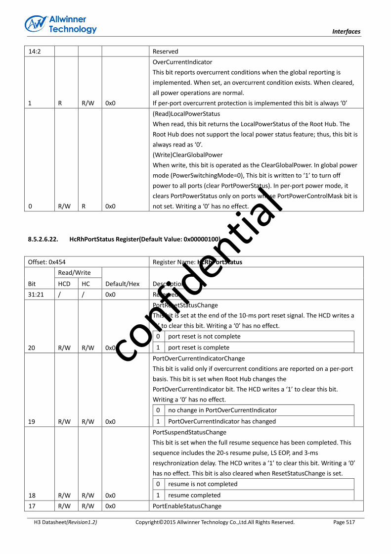
Interfaces
H3 Datasheet(Revision1.2) Copyright© 2015 Allwinner Technology Co.,Ltd.All Rights Reserved. Page 517
14:2 Reserved
1 R R/W 0x0
OverCurrentIndicator
This bit reports overcurrent conditions when the global reporting is
implemented. When set, an overcurrent condition exists. When cleared,
all power operations are normal.
If per-port overcurrent protection is implemented this bit is always ‘0’
0 R/W R 0x0
(Read)LocalPowerStatus
When read, this bit returns the LocalPowerStatus of the Root Hub. The
Root Hub does not support the local power status feature; thus, this bit is
always read as ‘0’.
(Write)ClearGlobalPower
When write, this bit is operated as the ClearGlobalPower. In global power
mode (PowerSwitchingMode=0), This bit is written to ‘1’ to turn off
power to all ports (clear PortPowerStatus). In per-port power mode, it
clears PortPowerStatus only on ports whose PortPowerControlMask bit is
not set. Writing a ‘0’ has no effect.
8.5.2.6.22. HcRhPortStatus Register(Default Value: 0x00000100)
Offset: 0x454 Register Name: HcRhPortStatus
Bit
Read/Write
Default/Hex Description HCD HC
31:21 / / 0x0 Reserved
20 R/W R/W 0x0
PortResetStatusChange
This bit is set at the end of the 10-ms port reset signal. The HCD writes a
‘1’ to clear this bit. Writing a ‘0’ has no effect.
0 port reset is not complete
1 port reset is complete
19 R/W R/W 0x0
PortOverCurrentIndicatorChange
This bit is valid only if overcurrent conditions are reported on a per-port
basis. This bit is set when Root Hub changes the
PortOverCurrentIndicator bit. The HCD writes a ‘1’ to clear this bit.
Writing a ‘0’ has no effect.
0 no change in PortOverCurrentIndicator
1 PortOverCurrentIndicator has changed
18 R/W R/W 0x0
PortSuspendStatusChange
This bit is set when the full resume sequence has been completed. This
sequence includes the 20-s resume pulse, LS EOP, and 3-ms
resychronization delay. The HCD writes a ‘1’ to clear this bit. Writing a ‘0’
has no effect. This bit is also cleared when ResetStatusChange is set.
0 resume is not completed
1 resume completed
17 R/W R/W 0x0 PortEnableStatusChange
confid
ential

Interfaces
H3 Datasheet(Revision1.2) Copyright© 2015 Allwinner Technology Co.,Ltd.All Rights Reserved. Page 518
This bit is set when hardware events cause the PortEnableStatus bit to be
cleared. Changes from HCD writes do not set this bit. The HCD writes a ‘1’
to clear this bit. Writing a ‘0’ has no effect.
0 no change in PortEnableStatus
1 change in PortEnableStatus
16 R/W R/W 0x0
ConnectStatusChange
This bit is set whenever a connect or disconnect event occurs. The HCD
writes a ‘1’ to clear this bit. Writing a ‘0’ has no effect. If
CurrentConnectStatus is cleared when a SetPortReset,SetPortEnable, or
SetPortSuspend write occurs, this bit is set to force the driver to
re-evaluate the connection status since these writes should not occur if
the port is disconnected.
0 no change in PortEnableStatus
1 change in PortEnableStatus
Note: If the DeviceRemovable[NDP] bit is set, this bit is set only
after a Root Hub reset to inform the system that the device is attached.
15:10 / / 0x0 Reserved
9 R/W R/W -
(read)LowSpeedDeviceAttached
This bit indicates the speed of the device attached to this port. When set,
a Low Speed device is attached to this port. When clear, a Full Speed
device is attached to this port. This field is valid only when the
CurrentConnectStatus is set.
0 full speed device attached
1 low speed device attached
(write)ClearPortPower
The HCD clears the PortPowerStatus bit by writing a ‘1’ to this bit. Writing
a ‘0’ has no effect.
8 R/W R/W 0x1
(read)PortPowerStatus
This bit reflects the port’s power status, regardless of the type of power
switching implemented. This bit is cleared if an overcurrent condition is
detected. HCD sets this bit by writing SetPortPower or SetGlobalPower.
HCD clears this bit by writing ClearPortPower or ClearGlobalPower. Which
power control switches are enabled is determined by
PowerSwitchingMode and
PortPortControlMask[NumberDownstreamPort]. In global switching
mode(PowerSwitchingMode=0), only Set/ClearGlobalPower controls
this bit. In per-port power switching (PowerSwitchingMode=1), if the
PortPowerControlMask[NDP] bit for the port is set, only
Set/ClearPortPower commands are enabled. If the mask is not set, only
Set/ClearGlobalPower commands are enabled. When port power is
disabled, CurrentConnectStatus, PortEnableStatus, PortSuspendStatus,
and PortResetStatus should be reset.
confid
ential
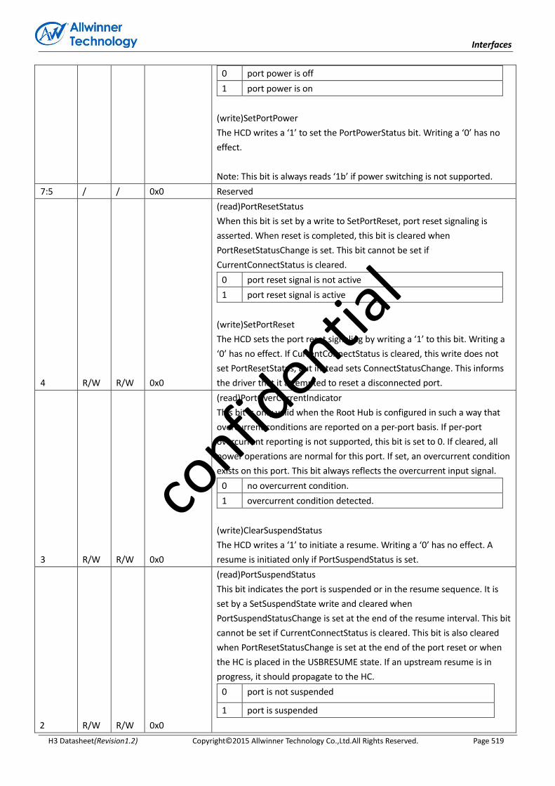
Interfaces
H3 Datasheet(Revision1.2) Copyright© 2015 Allwinner Technology Co.,Ltd.All Rights Reserved. Page 519
0 port power is off
1 port power is on
(write)SetPortPower
The HCD writes a ‘1’ to set the PortPowerStatus bit. Writing a ‘0’ has no
effect.
Note: This bit is always reads ‘1b’ if power switching is not supported.
7:5 / / 0x0 Reserved
4 R/W R/W 0x0
(read)PortResetStatus
When this bit is set by a write to SetPortReset, port reset signaling is
asserted. When reset is completed, this bit is cleared when
PortResetStatusChange is set. This bit cannot be set if
CurrentConnectStatus is cleared.
0 port reset signal is not active
1 port reset signal is active
(write)SetPortReset
The HCD sets the port reset signaling by writing a ‘1’ to this bit. Writing a
‘0’ has no effect. If CurrentConnectStatus is cleared, this write does not
set PortResetStatus, but instead sets ConnectStatusChange. This informs
the driver that it attempted to reset a disconnected port.
3 R/W R/W 0x0
(read)PortOverCurrentIndicator
This bit is only valid when the Root Hub is configured in such a way that
overcurrent conditions are reported on a per-port basis. If per-port
overcurrent reporting is not supported, this bit is set to 0. If cleared, all
power operations are normal for this port. If set, an overcurrent condition
exists on this port. This bit always reflects the overcurrent input signal.
0 no overcurrent condition.
1 overcurrent condition detected.
(write)ClearSuspendStatus
The HCD writes a ‘1’ to initiate a resume. Writing a ‘0’ has no effect. A
resume is initiated only if PortSuspendStatus is set.
2 R/W R/W 0x0
(read)PortSuspendStatus
This bit indicates the port is suspended or in the resume sequence. It is
set by a SetSuspendState write and cleared when
PortSuspendStatusChange is set at the end of the resume interval. This bit
cannot be set if CurrentConnectStatus is cleared. This bit is also cleared
when PortResetStatusChange is set at the end of the port reset or when
the HC is placed in the USBRESUME state. If an upstream resume is in
progress, it should propagate to the HC.
0 port is not suspended
1 port is suspended
confid
ential

Interfaces
H3 Datasheet(Revision1.2) Copyright© 2015 Allwinner Technology Co.,Ltd.All Rights Reserved. Page 520
(write)SetPortSuspend
The HCD sets the PortSuspendStatus bit by writing a ‘1’ to this bit. Writing
a ‘0’ has no effect. If CurrentConnectStatus is cleared, this write does not
set PortSuspendStatus; instead it sets ConnectStatusChange. This informs
the driver that it attempted to suspend a disconnected port.
1 R/W R/W 0x0
(read)PortEnableStatus
This bit indicates whether the port is enabled or disabled. The Root Hub
may clear this bit when an overcurrent condition, disconnect event,
switched-off power, or operational bus error such as babble is detected.
This change also causes PortEnabledStatusChange to be set. HCD sets this
bit by writing SetPortEnable and clears it by writing ClearPortEnable. This
bit cannot be set when CurrentConnectStatus is cleared. This bit is also
set, if not already, at the completion of a port reset when
ResetStatusChange is set or port suspend when
SuspendStatusChange is set.
0 port is disabled
1 port is enabled
(write)SetPortEnable
The HCD sets PortEnableStatus by writing a ‘1’. Writing a ‘0’ has no effect.
If CurrentConnectStatus is cleared, this write does not set
PortEnableStatus, but instead sets ConnectStatusChange. This informs the
driver that it attempted to enable a disconnected Port.
0 R/W R/W 0x0
(read)CurrentConnectStatus
This bit reflects the current state of the downstream port.
0 No device connected
1 Device connected
(write)ClearPortEnable
The HCD writes a ‘1’ to clear the PortEnableStatus bit. Writing ‘0’ has no
effect. The CurrentConnectStatus is not affected by any write.
Note: This bit is always read ‘1’ when the attached device is
nonremovalble(DviceRemoveable[NumberDownstreamPort]).
8.5.2.7. HCI Interface Control and Status Register Description
8.5.2.7.1. HCI Interface Control Register(Default Value: 0x00000000)
Offset: 0x800 Register Name: HCI_ICR
Bit R/W Default/Hex Description
31:21 / / Reserved.
20 R/W 0 EHCI HS force
Set 1 to this field force the ehci enter the high speed mode during bus reset.
This field only valid when the bit 1 is set.
confid
ential

Interfaces
H3 Datasheet(Revision1.2) Copyright© 2015 Allwinner Technology Co.,Ltd.All Rights Reserved. Page 521
19:18 / / /
17 R/W 0 HSIC Connect detect
1 in this field enable the hsic phy to detect device connect pulse on the bus.
This field only valid when the bit 1 is set.
16 R/W 0 HSIC Connect Interrupt Enable
Enable the HSIC connect interrupt.
This field only valid when the bit 1 is set.
15:13 / / /
12 / / /
11 R/W 0 AHB Master interface INCR16 enable
1: Use INCR16 when appropriate
0: do not use INCR16,use other enabled INCRX or unspecified length burst
INCR
10 R/W 0 AHB Master interface INCR8 enable
1: Use INCR8 when appropriate
0: do not use INCR8,use other enabled INCRX or unspecified length burst
INCR
9 R/W 0 AHB Master interface burst type INCR4 enable
1: Use INCR4 when appropriate
0: do not use INCR4,use other enabled INCRX or unspecified length burst
INCR
8 R/W 0 AHB Master interface INCRX align enable
1: start INCRx burst only on burst x-align address
0: Start burst on any double word boundary
Note: This bit must enable if any bit of 11:9 is enabled
7:2 / / Reserved
1 R/W 0 HSIC
0:/
1:HSIC
This meaning is only valid when the controller is HCI1.
0 R/W 0 ULPI bypass enable。
1: Enable UTMI interface, disable ULPI interface(SP used utmi
interface)
0: Enable ULPI interface, disable UTMI interface
8.5.2.7.2. HSIC status Register(Default Value: 0x00000000)
Offset: 0x804 Register Name: HSIC_STATUS
Bit R/W Default/Hex Description
31:17 / / /
16 R/W 0
HSIC Connect Status
1 in this field indicates a device connect pulse being detected on the bus. This
field only valid when the EHCI HS force bit and the HSIC Phy Select bit is set.
confid
ential

Interfaces
H3 Datasheet(Revision1.2) Copyright© 2015 Allwinner Technology Co.,Ltd.All Rights Reserved. Page 522
When the HSIC Connect Interrupt Enable is set, 1 in this bit will generate an
interrupt to the system.
This register is valid on HCI1.
15:0 / / /
8.5.2.8. USB Host Clock Requirement
Name Description
HCLK System clock (provided by AHB bus clock). This clock needs to be >30MHz.
CLK60M Clock from PHY for HS SIE, is constant to be 60MHz.
CLK48M Clock from PLL for FS/LS SIE, is constant to be 48MHz.
confid
ential

Interfaces
H3 Datasheet(Revision1.2) Copyright© 2015 Allwinner Technology Co.,Ltd.All Rights Reserved. Page 523
8.6. I2S/PCM
8.6.1. Overview
The I2S/PCM Controller has been designed to transfer streaming audio-data between the system memory and the
codec chip. The controller supports standard I2S format, Left-justified Mode format, Right-justified Mode format, PCM
Mode format and TDM Mode format.
The I2S/PCM controller includes the following features:
Supports industry-standard AMBA Peripheral Bus (APB) and it is fully compliant with the AMBA Specification,
Revision 2.0
Support different sample period width in each interface when using LRCK and LRCKR at the same time
Support full-duplex synchronous work mode
Support Master / Slave mode
Support adjustable interface voltage
Support clock up to 100MHz
Support adjustable audio sample rate from 8-bit to 32-bit.
Support up to 8 slots which has adjustable width from 8-bit to 32-bit.
Support sample rate from 8KHz to 192KHz
Support 8-bits u-law and 8-bits A-law companded sample
One 128 x 32-bit width FIFO for data transmit, one 64 x 32-bit width FIFO for data receive
Support programmable PCM frame width: 1 BCLK width (short frame) and 2 BCLKs width (long frame)
Programmable FIFO thresholds
Interrupt and DMA Support
Support loopback mode for test
8.6.2. Signal Description
8.6.2.1. I2S/PCM Pin List
Signal Name(x=0,1) Direction(M) Description
PCMx_CLK O I2S/PCM x MCLK Output
PCMx_SYNC I/O I2S/PCM x Sample Rate Clock/Sync
PCMx_DIN I I2S/PCM x Serial Data Input
PCMx_DOUT O I2S/PCM x Serial Data Output
8.6.2.2. Digital Audio Interface Clock Source and Frequency
Name Description
confid
ential

Interfaces
H3 Datasheet(Revision1.2) Copyright© 2015 Allwinner Technology Co.,Ltd.All Rights Reserved. Page 524
Audio_PLL 24.576Mhz or 22.5792Mhz generated by AUDIO-PLL to produce 48KHz or 44.1KHz serial frequency
8.6.3. Functionalities Description
8.6.3.1. Typical Applications
The I2S/PCM provides a serial bus interface for stereo and multichannel audio data. This interface is most commonly
used by consumer audio market, including compact disc, digital audio tape, digital sound processors, and digital
TV-sound.
8.6.3.2. Functional Block Diagram
The I2S/PCM Interface block diagram is shown below:
Register
64x32-bits
RX FIFO
I2S
Engine
PCM
Engine
PCM
Codec
Clock
Divide
M
U
X
S
Y
N
C
MCLK
BCLK
BCLK
LRCK
SDO[3:0]
SDI
TX
_D
RQ
RX
_D
RQ
PLL2
DA
_IN
T
APB
128x32-
bits
TX FIFO
Figure 8-8. I2S/PCM Interface System Block Diagram
8.6.4. Timing Diagram
confid
ential

Interfaces
H3 Datasheet(Revision1.2) Copyright© 2015 Allwinner Technology Co.,Ltd.All Rights Reserved. Page 525
BCLK
LRCK
DOUT/DIN
n-1 … 1 0n-2MSB LSB
Left Channel Right Channel
1 / fs
8 slot
4 slot
2 slot 0 1
0
0
1
1
2
2
3
34 6 5 7
DOUT/DIN
DOUT/DIN[I2S mode]
m m = 0 ~ 7 slot
sample
[TDM-I2S mode]
[TDM-I2S mode]
Figure 8-9. Timing Diagram for I2S/TDM-I2S mode
BCLK
LRCK
n-1 … 1 0n-2MSB LSB
Left Channel Right Channel
1 / fs
8 slot
4 slot
2 slot 0 1
0
0
1
1
2
2
3
34 6 5 7
[Left-Justified mode]
m m = 0 ~ 7 slot
sample
[TDM-Left mode]
[TDM-Left mode]
Figure 8-10. Timing Diagram for Left-justified/TDM-Left mode
confid
ential
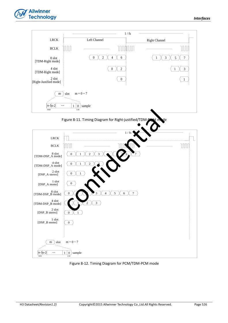
Interfaces
H3 Datasheet(Revision1.2) Copyright© 2015 Allwinner Technology Co.,Ltd.All Rights Reserved. Page 526
BCLK
LRCK
n-1 … 1 0n-2MSB LSB
Left Channel Right Channel
1 / fs
8 slot
4 slot
2 slot 0 1
0
0
1
1
2
2
3
34 6 5 7
[Right-Justified mode]
m m = 0 ~ 7 slot
sample
[TDM-Right mode]
[TDM-Right mode]
Figure 8-11. Timing Diagram for Right-justified/TDM-Right mode
BCLK
LRCK
n-1 … 1 0n-2MSB LSB
1 / fs
8 slot
4 slot
2 slot
0 1 2 3
[DSP_B stereo]
m m = 0 ~ 7 slot
sample
[TDM-DSP_B mode]
[TDM-DSP_B mode] 4 5 6 7
0 1 2 3
0 1
[DSP_B mono]1 slot
0
0 1 2 3 4 5 6 7
0 1 2 3
0 1
0
8 slot
4 slot
2 slot[DSP_A stereo]
[TDM-DSP_A mode]
[TDM-DSP_A mode]
[DSP_A mono]1 slot
Figure 8-12. Timing Diagram for PCM/TDM-PCM mode
confid
ential
Interfaces
H3 Datasheet(Revision1.2) Copyright© 2015 Allwinner Technology Co.,Ltd.All Rights Reserved. Page 527
8.6.5. Operation Modes
The software operation of the I2S/PCM is divided into five steps: system setup, PCM/I2S initialization, the channel setup,
DMA setup and Enable/Disable module. These five steps are described in detail in the following sections.
8.6.5.1. System setup and I2S/PCM initialization
The first step in the system setup is properly programming the GPIO. Because the I2S/PCM port is a multiplex pin. You
can find the function in the pin multiplex specification. The clock source for the I2S/PCM should be followed. At first you
must reset the audio PLL though the PLL_ENABLE bit of PLL_AUDIO_CTRL_REG in the CCU. The second step, you must
setup the frequence of the audio pll in the PLL_AUDIO_CTRL_REG. The configuration of audio pll can be found in the
chapter 4.3.5. After that, you must open the I2S/PCM gating though the I2S/PCM0_CLK_REG/I2S/PCM1_CLK_REG when
you checkout that the LOCK bit of PLL_AUDIO_CTRL_REG become 1. At last, you must reset the I2S/PCM in
BUS_SOFT_RST_REG3's bit[13:12] and open the I2S/PCM bus gating in the BUS_CLK_GATING_REG2's bit[13:12].
After the system setup, the register of I2S/PCM can be setup. At first, you should initialization the I2S/PCM. You should
closed the globe enable bit(I2S/PCM_CTL[0]) , TX enable bit(I2S/PCM_CTL[2]) and RX enable bit(I2S/PCM_CTL[1]) by
write 0 to it. After that, you must clear the TX/RX FIFO by write 0 to register I2S/PCM_FCTL[25:24]. At last, you can clear
the TX FIFO and RX FIFO counter by write 0 to I2S/PCM_TXCNT and I2S/CPM_RXCNT.
8.6.5.2. The channel setup and DMA setup
Before the usage and control of I2S/PCM, you must configure the I2C. The configuration of I2C will not describe in this
chapter. But you can only configure I2S/PCM of master and slave though the I2C. In the following, you can setup the
I2S/PCM of mater and slave. The configuration can be referred to the the protocol of I2S/PCM. Then, you can set the
translation mode, the sample precision, the wide of slot, the frame mode and the trigger level. The register set can be
found in the spec.
The I2S/PCM supports three methods to transfer the data. The most common way is DMA, the set of DMA can be found
in the DMA spec. In this module, you just to enable the DRQ.
8.6.5.3. Enable and disable the I2S/PCM
To enable the function, you can enable TX/RX by write the I2S/PCM_CTL[2:1]. After that, you must enable I2S/PCM by
write the Globe Enable bit to 1 in the I2S/PCM_CTL. The disable process is writed the Globe Enable to 0.
confid
ential

Interfaces
H3 Datasheet(Revision1.2) Copyright© 2015 Allwinner Technology Co.,Ltd.All Rights Reserved. Page 528
8.6.6. I2S/PCM Register List
Module Name Base Address
I2S/PCM 0 0x01C22000
I2S/PCM 1 0x01C22400
I2S/PCM 2 0x01C22800 (for HDMI)
Register Name Offset Description
I2S/PCM_CTL 0x00 I2S/PCM Control Register
I2S/PCM_FMT0 0x04 I2S/PCM Format Register 0
I2S/PCM_FMT1 0x08 I2S/PCM Format Register 1
I2S/PCM_ISTA 0x0C I2S/PCM Interrupt Status Register
I2S/PCM_RXFIFO 0x10 I2S/PCM RX FIFO Register
I2S/PCM_FCTL 0x14 I2S/PCM FIFO Control Register
I2S/PCM_FSTA 0x18 I2S/PCM FIFO Status Register
I2S/PCM_INT 0x1C I2S/PCM DMA & Interrupt Control Register
I2S/PCM_TXFIFO 0x20 I2S/PCM TX FIFO Register
I2S/PCM_CLKD 0x24 I2S/PCM Clock Divide Register
I2S/PCM_TXCNT 0x28 I2S/PCM TX Sample Counter Register
I2S/PCM_RXCNT 0x2C I2S/PCM RX Sample Counter Register
I2S/PCM_CHCFG 0x30 I2S/PCM Channel Configuration register
I2S/PCM_TX0CHCFG 0x34 I2S/PCM TX0 Channel Configuration register
I2S/PCM_TX1CHSEL 0x38 I2S/PCM TX1 Channel Select Register
I2S/PCM_TX2CHSEL 0x3C I2S/PCM TX2 Channel Select Register
I2S/PCM_TX3CHSEL 0x40 I2S/PCM TX3 Channel Select Register
I2S/PCM_TX0CHMAP 0x44 I2S/PCM TX0 Channel Mapping Register
I2S/PCM_TX0CHMAP 0x48 I2S/PCM TX1 Channel Mapping Register
I2S/PCM_TX0CHMAP 0x4C I2S/PCM TX2 Channel Mapping Register
I2S/PCM_TX0CHMAP 0x50 I2S/PCM TX3 Channel Mapping Register
I2S/PCM_RXCHSEL 0x54 I2S/PCM RX Channel Select register
I2S/PCM_RXCHMAP 0x58 I2S/PCM RX Channel Mapping Register
8.6.7. I2S/PCM Register Description
8.6.7.1. I2S/PCM Control Register(Default Value: 0x00060000)
Offset: 0x00 Register Name: I2S/PCM_CTL
Bit R/W Default/Hex Description
31:19 / / /
18 R/W 1
BCLK_OUT
0: input
confid
ential

Interfaces
H3 Datasheet(Revision1.2) Copyright© 2015 Allwinner Technology Co.,Ltd.All Rights Reserved. Page 529
1: output
17 R/W 1
LRCK_OUT
0: input
1: output
16 R/W 0
LRCKR_OUT
0: input
1: output
15:12 / / /
11 R/W 0 /
10 R/W 0 /
9 R/W 0 /
8 R/W 0
SDO0_EN
0: Disable, Hi-Z state
1: Enable
7 / / /
6 R/W 0
OUT Mute
0: normal transfer
1: force DOUT to output 0
5:4 R/W 0
MODE_SEL
Mode Selection
0: PCM mode (offset 0: DSP_B; offset 1: DSP_A)
1: Left mode (offset 0: LJ mode; offset 1: I2S mode)
2: Right-Justified mode
3: Reserved
3 R/W 0
LOOP
Loop back test
0: Normal mode
1: Loop back test
When set ‘1’, connecting the SDO0 with the SDI
2 R/W 0
TXEN
Transmitter Block Enable
0: Disable
1: Enable
1 R/W 0
RXEN
Receiver Block Enable
0: Disable
1: Enable
0 R/W 0
GEN
Globe Enable
A disable on this bit overrides any other block or channel enables.
0: Disable
1: Enable
confid
ential
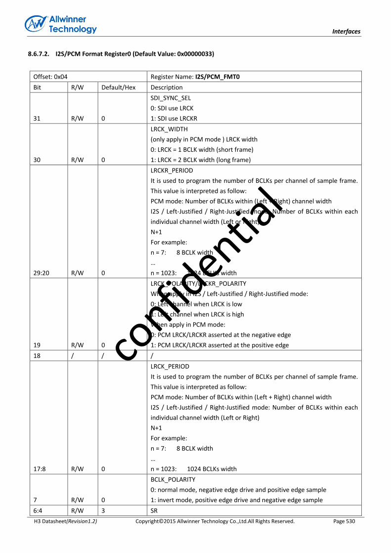
Interfaces
H3 Datasheet(Revision1.2) Copyright© 2015 Allwinner Technology Co.,Ltd.All Rights Reserved. Page 530
8.6.7.2. I2S/PCM Format Register0 (Default Value: 0x00000033)
Offset: 0x04 Register Name: I2S/PCM_FMT0
Bit R/W Default/Hex Description
31 R/W 0
SDI_SYNC_SEL
0: SDI use LRCK
1: SDI use LRCKR
30 R/W 0
LRCK_WIDTH
(only apply in PCM mode ) LRCK width
0: LRCK = 1 BCLK width (short frame)
1: LRCK = 2 BCLK width (long frame)
29:20 R/W 0
LRCKR_PERIOD
It is used to program the number of BCLKs per channel of sample frame.
This value is interpreted as follow:
PCM mode: Number of BCLKs within (Left + Right) channel width
I2S / Left-Justified / Right-Justified mode: Number of BCLKs within each
individual channel width (Left or Right)
N+1
For example:
n = 7: 8 BCLK width
…
n = 1023: 1024 BCLKs width
19 R/W 0
LRCK_POLARITY/LRCKR_POLARITY
When apply in I2S / Left-Justified / Right-Justified mode:
0: Left channel when LRCK is low
1: Left channel when LRCK is high
When apply in PCM mode:
0: PCM LRCK/LRCKR asserted at the negative edge
1: PCM LRCK/LRCKR asserted at the positive edge
18 / / /
17:8 R/W 0
LRCK_PERIOD
It is used to program the number of BCLKs per channel of sample frame.
This value is interpreted as follow:
PCM mode: Number of BCLKs within (Left + Right) channel width
I2S / Left-Justified / Right-Justified mode: Number of BCLKs within each
individual channel width (Left or Right)
N+1
For example:
n = 7: 8 BCLK width
…
n = 1023: 1024 BCLKs width
7 R/W 0
BCLK_POLARITY
0: normal mode, negative edge drive and positive edge sample
1: invert mode, positive edge drive and negative edge sample
6:4 R/W 3 SR
confid
ential

Interfaces
H3 Datasheet(Revision1.2) Copyright© 2015 Allwinner Technology Co.,Ltd.All Rights Reserved. Page 531
Sample Resolution
0: Reserved
1: 8-bit
2: 12-bit
3: 16-bit
4: 20-bit
5: 24-bit
6: 28-bit
7: 32-bit
3 R/W 0
EDGE_TRANSFER
0: SDO drive data and SDI sample data at the different BCLK edge
1: SDO drive data and SDI sample data at the same BCLK edge
BCLK_POLARITY = 0, use negative edge
BCLK_POLARITY = 1, use positive edge
2:0 R/W 0x3
SW
Slot Width Select
0: Reserved
1: 8-bit
2: 12-bit
3: 16-bit
4: 20-bit
5: 24-bit
6: 28-bit
7: 32-bit
8.6.7.3. I2S/PCM Format Register1 (Default Value: 0x00000030)
Offset: 0x08 Register Name: I2S/PCM_FMT1
Bit R/W Default/Hex Description
31:8 / /
7 R/W 0
RX MLS
MSB / LSB First Select
0: MSB First
1: LSB First
6 R/W 0
TX MLS
MSB / LSB First Select
0: MSB First
1: LSB First
5:4 R/W 3
SEXT
Sign Extend in slot [sample resolution < slot width]
0: Zeros or audio gain padding at LSB position
1: Sign extension at MSB position
2: Reserved
3: Transfer 0 after each sample in each slot
confid
ential
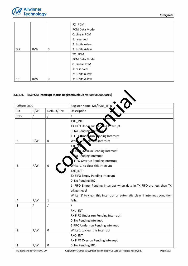
Interfaces
H3 Datasheet(Revision1.2) Copyright© 2015 Allwinner Technology Co.,Ltd.All Rights Reserved. Page 532
3:2 R/W 0
RX_PDM
PCM Data Mode
0: Linear PCM
1: reserved
2: 8-bits u-law
3: 8-bits A-law
1:0 R/W 0
TX_PDM
PCM Data Mode
0: Linear PCM
1: reserved
2: 8-bits u-law
3: 8-bits A-law
8.6.7.4. I2S/PCM Interrupt Status Register(Default Value: 0x00000010)
Offset: 0x0C Register Name: I2S/PCM_ISTA
Bit R/W Default/Hex Description
31:7 / / /
6 R/W 0
TXU_INT
TX FIFO Under run Pending Interrupt
0: No Pending Interrupt
1: FIFO Under run Pending Interrupt
Write 1 to clear this interrupt
5 R/W 0
TXO_INT
TX FIFO Overrun Pending Interrupt
0: No Pending Interrupt
1: FIFO Overrun Pending Interrupt
Write ‘1’ to clear this interrupt
4 R/W 1
TXE_INT
TX FIFO Empty Pending Interrupt
0: No Pending IRQ
1: FIFO Empty Pending Interrupt when data in TX FIFO are less than TX
trigger level
Write ‘1’ to clear this interrupt or automatic clear if interrupt condition
fails.
3 / / /
2 R/W 0
RXU_INT
RX FIFO Under run Pending Interrupt
0: No Pending Interrupt
1:FIFO Under run Pending Interrupt
Write 1 to clear this interrupt
1 R/W 0
RXO_INT
RX FIFO Overrun Pending Interrupt
0: No Pending IRQ
confid
ential

Interfaces
H3 Datasheet(Revision1.2) Copyright© 2015 Allwinner Technology Co.,Ltd.All Rights Reserved. Page 533
1: FIFO Overrun Pending IRQ
Write ‘1’ to clear this interrupt
0 R/W 0
RXA_INT
RX FIFO Data Available Pending Interrupt
0: No Pending IRQ
1: Data Available Pending IRQ when data in RX FIFO are more than RX
trigger level
Write ‘1’ to clear this interrupt or automatic clear if interrupt condition
fails.
8.6.7.5. I2S/PCM RX FIFO Register(Default Value: 0x00000000)
Offset: 0x10 Register Name: I2S/PCM_RXFIFO
Bit R/W Default/Hex Description
31:0 R 0
RX_DATA
RX Sample
Host can get one sample by reading this register. The left channel sample
data is first and then the right channel sample.
8.6.7.6. I2S/PCM FIFO Control Register (Default Value: 0x000400F0)
Offset: 0x14 Register Name: I2S/PCM_FCTL
Bit R/W Default/Hex Description
31 R/W 0
HUB_EN
Audio hub enable
0:disable
1:enable
30:26 / / /
25 R/W 0
FTX
Write ‘1’ to flush TX FIFO, self clear to ‘0’.
24 R/W 0
FRX
Write ‘1’ to flush RX FIFO, self clear to ‘0’.
23:19 / / /
18:12 R/W 0x40
TXTL
TX FIFO Empty Trigger Level
Interrupt and DMA request trigger level for TXFIFO normal condition
Trigger Level = TXTL
11:10 / / /
9:4 R/W 0xF
RXTL
RX FIFO Trigger Level
Interrupt and DMA request trigger level for RXFIFO normal condition
Trigger Level = RXTL + 1
confid
ential

Interfaces
H3 Datasheet(Revision1.2) Copyright© 2015 Allwinner Technology Co.,Ltd.All Rights Reserved. Page 534
3 / / /
2 R/W 0
TXIM
TX FIFO Input Mode (Mode 0, 1)
0: Valid data at the MSB of TXFIFO register
1: Valid data at the LSB of TXFIFO register
Example for 20-bits transmitted audio sample:
Mode 0: FIFO_I[31:0] = {APB_WDATA[31:12], 12’h0}
Mode 1: FIFO_I[31:0] = {APB_WDATA[19:0], 12’h0}
1:0 R/W 0
RXOM
RX FIFO Output Mode (Mode 0, 1, 2, 3)
00: Expanding ‘0’ at LSB of DA_RXFIFO register.
01: Expanding received sample sign bit at MSB of DA_RXFIFO register.
10: Truncating received samples at high half-word of DA_RXFIFO register
and low half-word of DA_RXFIFO register is filled by ‘0’.
11: Truncating received samples at low half-word of DA_RXFIFO register
and high half-word of DA_RXFIFO register is expanded by its sign bit.
Example for 20-bits received audio sample:
Mode 0: APB_RDATA[31:0] = {FIFO_O[31:12], 12’h0}
Mode 1: APB_RDATA [31:0] = {12{FIFO_O[31]}, FIFO_O[31:12]}
Mode 2: APB_RDATA [31:0] = {FIFO_O[31:16], 16’h0}
Mode 3: APB_RDATA [31:0] = {16{FIFO_O[31], FIFO_O[31:16]}
8.6.7.7. I2S/PCM FIFO Status Register (Default Value: 0x10800000)
Offset: 0x18 Register Name: I2S/PCM_FSTA
Bit R/W Default/Hex Description
31:29 / / /
28 R 1
TXE
TX FIFO Empty
0: No room for new sample in TX FIFO
1: More than one room for new sample in TX FIFO (>= 1 word)
27:24 / / /
23:16 R 0x80
TXE_CNT
TX FIFO Empty Space Word Counter
15:9 / / /
8 R 0
RXA
RX FIFO Available
0: No available data in RX FIFO
1: More than one sample in RX FIFO (>= 1 word)
7 / / /
6:0 R 0
RXA_CNT
RX FIFO Available Sample Word Counter
confid
ential
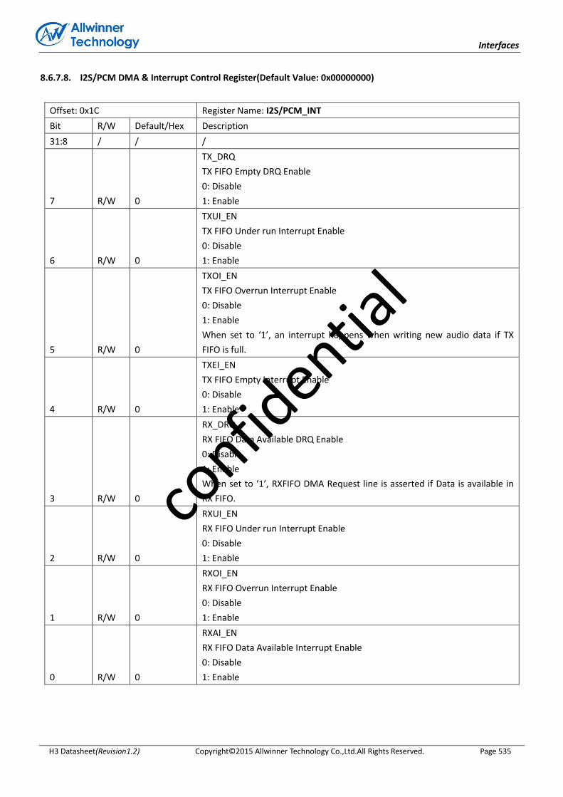
Interfaces
H3 Datasheet(Revision1.2) Copyright© 2015 Allwinner Technology Co.,Ltd.All Rights Reserved. Page 535
8.6.7.8. I2S/PCM DMA & Interrupt Control Register(Default Value: 0x00000000)
Offset: 0x1C Register Name: I2S/PCM_INT
Bit R/W Default/Hex Description
31:8 / / /
7 R/W 0
TX_DRQ
TX FIFO Empty DRQ Enable
0: Disable
1: Enable
6 R/W 0
TXUI_EN
TX FIFO Under run Interrupt Enable
0: Disable
1: Enable
5 R/W 0
TXOI_EN
TX FIFO Overrun Interrupt Enable
0: Disable
1: Enable
When set to ‘1’, an interrupt happens when writing new audio data if TX
FIFO is full.
4 R/W 0
TXEI_EN
TX FIFO Empty Interrupt Enable
0: Disable
1: Enable
3 R/W 0
RX_DRQ
RX FIFO Data Available DRQ Enable
0: Disable
1: Enable
When set to ‘1’, RXFIFO DMA Request line is asserted if Data is available in
RX FIFO.
2 R/W 0
RXUI_EN
RX FIFO Under run Interrupt Enable
0: Disable
1: Enable
1 R/W 0
RXOI_EN
RX FIFO Overrun Interrupt Enable
0: Disable
1: Enable
0 R/W 0
RXAI_EN
RX FIFO Data Available Interrupt Enable
0: Disable
1: Enable
confid
ential

Interfaces
H3 Datasheet(Revision1.2) Copyright© 2015 Allwinner Technology Co.,Ltd.All Rights Reserved. Page 536
8.6.7.9. I2S/PCM TX FIFO Register(Default Value: 0x00000000)
Offset: 0x20 Register Name: I2S/PCM_TXFIFO
Bit R/W Default/Hex Description
31:0 W 0
TX_DATA
TX Sample
Transmitting left, right channel sample data should be written this register
one by one. The left channel sample data is first and then the right channel
sample.
8.6.7.10. I2S/PCM Clock Divide Register(Default Value: 0x00000000)
Offset: 0x24 Register Name: I2S/PCM_CLKD
Bit R/W Default/Hex Description
31:9 / / /
8 R/W 0
MCLKO_EN
0: Disable MCLK Output
1: Enable MCLK Output
Notes: Whether in Slave or Master mode, when this bit is set to 1, MCLK
should be output.
7:4 R/W 0
BCLKDIV
BCLK Divide Ratio from PLL2
0: reserved
1: Divide by 1
2: Divide by 2
3: Divide by 4
4: Divide by 6
5: Divide by 8
6: Divide by 12
7: Divide by 16
8: Divide by 24
9: Divide by 32
10: Divide by 48
11: Divide by 64
12: Divide by 96
13: Divide by 128
14: Divide by 176
15: Divide by 192
3:0 R/W 0
MCLKDIV
MCLK Divide Ratio from PLL2 Output
0: reserved
1: Divide by 1
2: Divide by 2
confid
ential

Interfaces
H3 Datasheet(Revision1.2) Copyright© 2015 Allwinner Technology Co.,Ltd.All Rights Reserved. Page 537
3: Divide by 4
4: Divide by 6
5: Divide by 8
6: Divide by 12
7: Divide by 16
8: Divide by 24
9: Divide by 32
10: Divide by 48
11: Divide by 64
12: Divide by 96
13: Divide by 128
14: Divide by 176
15: Divide by 192
8.6.7.11. I2S/PCM TX Counter Register(Default Value: 0x00000000)
Offset: 0x28 Register Name: I2S/PCM_TXCNT
Bit R/W Default/Hex Description
31:0 R/W 0
TX_CNT
TX Sample Counter
The audio sample number of sending into TXFIFO. When one sample is put
into TXFIFO by DMA or by host IO, the TX sample counter register increases
by one. The TX sample counter register can be set to any initial valve at any
time. After been updated by the initial value, the counter register should
count on base of this initial value.
8.6.7.12. I2S/PCM RX Counter Register(Default Value: 0x00000000)
Offset: 0x2C Register Name: I2S/PCM_RXCNT
Bit R/W Default/Hex Description
31:0 R/W 0
RX_CNT
RX Sample Counter
The audio sample number of writing into RXFIFO. When one sample is
written by Digital Audio Engine, the RX sample counter register increases by
one. The RX sample counter register can be set to any initial valve at any
time. After been updated by the initial value, the counter register should
count on base of this initial value.
8.6.7.13. I2S/PCM Channel Configuration Register(Default Value: 0x00000000)
Offset: 0x30 Register Name: I2S/PCM_CHCFG
confid
ential

Interfaces
H3 Datasheet(Revision1.2) Copyright© 2015 Allwinner Technology Co.,Ltd.All Rights Reserved. Page 538
Bit R/W Default/Hex Description
31:10 / / /
9 R/W 0
TX_SLOT_HIZ
0: normal mode for the last half cycle of BCLK in the slot
1: turn to hi-z state for the last half cycle of BCLK in the slot
8 R/W 0
TXn_STATE
0: transfer level 0 when not transferring slot
1: turn to hi-z state when not transferring slot
7 / / /
6:4 R/W 0
RX_SLOT_NUM
RX Channel/Slot Number which between CPU/DMA and FIFO
0: 1 channel or slot
...
7: 8 channels or slots
3 / / /
2:0 R/W 0
TX_SLOT_NUM
TX Channel/Slot Number which between CPU/DMA and FIFO
0: 1 channel or slot
...
7: 8 channels or slots
8.6.7.14. I2S/PCM TXn Channel Select Register(Default Value: 0x00000000)
Offset: 0x34 + n*4 (n = 0, 1, 2, 3) Register Name: I2S/PCM_TXnCHSEL
Bit R/W Default/Hex Description
31:14 / / /
13:12 R/W 0 TXn_OFFSET
TXn offset tune, TXn data offset to LRCK
0: no offset
n: data is offset by n BCLKs to LRCK
11:4 R/W 0 TXn_CHEN
TXn Channel (slot) enable, bit[11:4] refer to slot [7:0]. When one or more
slot(s) is(are) disabled, the affected slot(s) is(are) set to disable state
0: disable
1: enable
3 / / /
2:0 R/W 0
TXn_CHSEL
TXn Channel (slot) number Select for each output
0: 1 channel / slot
…
7: 8 channels / slots
confid
ential

Interfaces
H3 Datasheet(Revision1.2) Copyright© 2015 Allwinner Technology Co.,Ltd.All Rights Reserved. Page 539
8.6.7.15. I2S/PCM TXn Channel Mapping Register(Default Value: 0x00000000)
Offset: 0x44 + n*4 (n = 0, 1, 2, 3) Register Name: I2S/PCM_TXnCHMAP
Bit R/W Default/Hex Description
31 / / /
30:28 R/W 0 TXn_CH7_MAP
TXn Channel7 Mapping
0: 1st sample
…
7: 8th sample
27 / / /
26:24 R/W 0 TXn_CH6_MAP
TXn Channel6 Mapping
0: 1st sample
…
7: 8th sample
23 / / /
22:20 R/W 0 TXn_CH5_MAP
TXn Channel5 Mapping
0: 1st sample
…
7: 8th sample
19 / / /
18:16 R/W 0 TXn_CH4_MAP
TXn Channel4 Mapping
0: 1st sample
…
7: 8th sample
15 / / /
14:12 R/W 0 TXn_CH3_MAP
TXn Channel3 Mapping
0: 1st sample
…
7: 8th sample
11 / / /
10:8 R/W 0 TXn_CH2_MAP
TXn Channel2 Mapping
0: 1st sample
…
7: 8th sample
7 / / /
6:4 R/W 0 TXn_CH1_MAP
TXn Channel1 Mapping
0: 1st sample
confid
ential
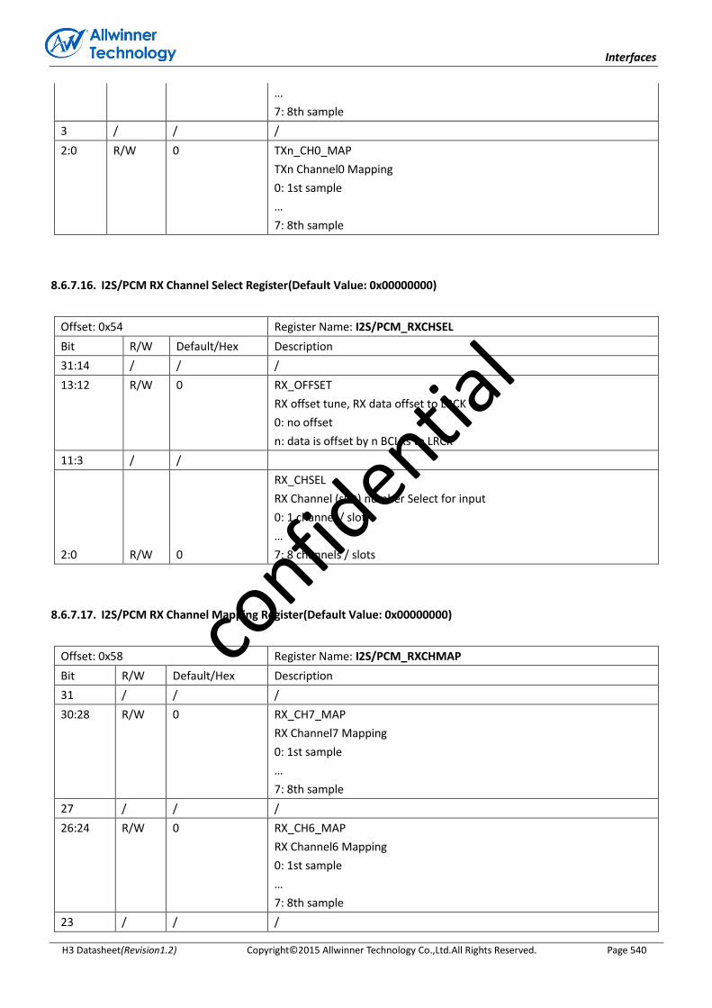
Interfaces
H3 Datasheet(Revision1.2) Copyright© 2015 Allwinner Technology Co.,Ltd.All Rights Reserved. Page 540
…
7: 8th sample
3 / / /
2:0 R/W 0 TXn_CH0_MAP
TXn Channel0 Mapping
0: 1st sample
…
7: 8th sample
8.6.7.16. I2S/PCM RX Channel Select Register(Default Value: 0x00000000)
Offset: 0x54 Register Name: I2S/PCM_RXCHSEL
Bit R/W Default/Hex Description
31:14 / / /
13:12 R/W 0 RX_OFFSET
RX offset tune, RX data offset to LRCK
0: no offset
n: data is offset by n BCLKs to LRCK
11:3 / /
2:0 R/W 0
RX_CHSEL
RX Channel (slot) number Select for input
0: 1 channel / slot
…
7: 8 channels / slots
8.6.7.17. I2S/PCM RX Channel Mapping Register(Default Value: 0x00000000)
Offset: 0x58 Register Name: I2S/PCM_RXCHMAP
Bit R/W Default/Hex Description
31 / / /
30:28 R/W 0 RX_CH7_MAP
RX Channel7 Mapping
0: 1st sample
…
7: 8th sample
27 / / /
26:24 R/W 0 RX_CH6_MAP
RX Channel6 Mapping
0: 1st sample
…
7: 8th sample
23 / / /
confid
ential
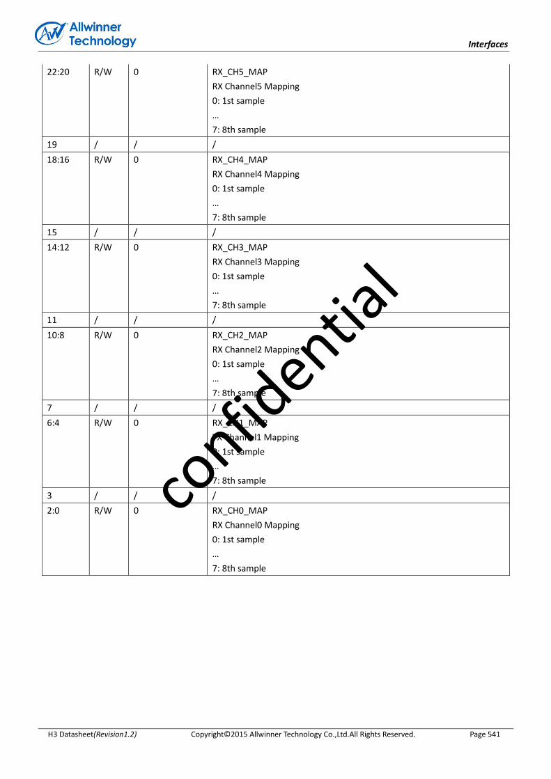
Interfaces
H3 Datasheet(Revision1.2) Copyright© 2015 Allwinner Technology Co.,Ltd.All Rights Reserved. Page 541
22:20 R/W 0 RX_CH5_MAP
RX Channel5 Mapping
0: 1st sample
…
7: 8th sample
19 / / /
18:16 R/W 0 RX_CH4_MAP
RX Channel4 Mapping
0: 1st sample
…
7: 8th sample
15 / / /
14:12 R/W 0 RX_CH3_MAP
RX Channel3 Mapping
0: 1st sample
…
7: 8th sample
11 / / /
10:8 R/W 0 RX_CH2_MAP
RX Channel2 Mapping
0: 1st sample
…
7: 8th sample
7 / / /
6:4 R/W 0 RX_CH1_MAP
TX Channel1 Mapping
0: 1st sample
…
7: 8th sample
3 / / /
2:0 R/W 0 RX_CH0_MAP
RX Channel0 Mapping
0: 1st sample
…
7: 8th sample
confid
ential

Interfaces
H3 Datasheet(Revision1.2) Copyright© 2015 Allwinner Technology Co.,Ltd.All Rights Reserved. Page 542
8.7. OWA
8.7.1. Overview
The OWA(One Wire Audio) provides a serial bus interface for audio data between system. This interface is widely used
for consumer audio connect.
The OWA includes the following features:
IEC-60958 transmitter and receiver functionality
Complies with SPDIF Interface
Support channel status insertion for the transmitter
Hardware Parity generation on the transmitter
One 32×24bits FIFO (TX) for audio data transfer
Programmable FIFO thresholds
Interrupt and DMA support
8.7.2. Functional Description
8.7.2.1. OWA Interface Pin List
Signal Name Direction(M) Description Pin
OWA_DOUT O OWA output PA17
8.7.2.2. OWA Clock Requirement
Clock Name Description Requirement
apb_clk APB bus clock >13 MHz
s_clk OWA serial access clock 4x24.576 MHz or 4x22.5792 MHz from CCU
8.7.2.3. OWA Block Diagram
Figure 8-13 shows the OWA block diagram.
confid
ential
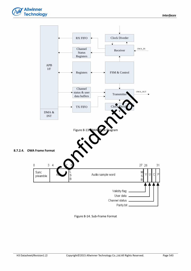
Interfaces
H3 Datasheet(Revision1.2) Copyright© 2015 Allwinner Technology Co.,Ltd.All Rights Reserved. Page 543
APB
I/F
RX FIFO
Channel
Status
Registers
Registers
TX FIFO
Channel
status & user
data buffers
DMA &
INT
OWA_IN
OWA_OUT
Receiver
Transmitter
FSM & Control
Clock Divider
Clock Diveder
Figure 8-13. OWA Block Diagram
8.7.2.4. OWA Frame Format
Figure 8-14. Sub-Frame Format
confid
ential
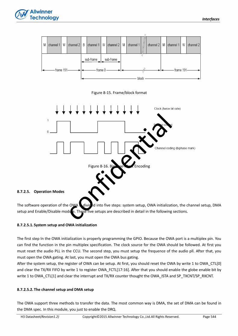
Interfaces
H3 Datasheet(Revision1.2) Copyright© 2015 Allwinner Technology Co.,Ltd.All Rights Reserved. Page 544
Figure 8-15. Frame/block format
Figure 8-16. Biphase-Mark Encoding
8.7.2.5. Operation Modes
The software operation of the OWA is divided into five steps: system setup, OWA initialization, the channel setup, DMA
setup and Enable/Disable module. These five setups are described in detail in the following sections.
8.7.2.5.1. System setup and OWA initialization
The first step In the OWA initialization is properly programming the GPIO. Because the OWA port is a multiplex pin. You
can find the function in the pin multiplex specification. The clock source for the OWA should be followed. At first you
must reset the audio PLL in the CCU. The second step, you must setup the frequence of the audio pll. After that, you
must open the OWA gating. At last, you must open the OWA bus gating.
After the system setup, the register of OWA can be setup. At first, you should reset the OWA by write 1 to OWA_CTL[0]
and clear the TX/RX FIFO by write 1 to register OWA_FCTL[17:16]. After that you should enable the globe enable bit by
write 1 to OWA_CTL[1] and clear the interrupt and TX/RX counter thought the OWA_ISTA and SP_TXCNT/SP_RXCNT.
8.7.2.5.2. The channel setup and DMA setup
The OWA support three methods to transfer the data. The most common way is DMA, the set of DMA can be found in
the DMA spec. In this module, you just to enable the DRQ.
confid
ential

Interfaces
H3 Datasheet(Revision1.2) Copyright© 2015 Allwinner Technology Co.,Ltd.All Rights Reserved. Page 545
8.7.2.5.3. Enable and disable the OWA
To enable the function, you can enable TX/RX by write the OWA_TX_CFIG[31] and OWA_RX_CFIG[0]. After that, you
must enable OWA by write the Globe Enable bit to 1 in the OWA_CTL.The disable process is write the Globe Enable to 0.
8.7.3. OWA Register List
Module Name Base Address
OWA 0x01C21000
Register Name Offset Description
OWA_GEN_CTL 0x00 OWA General Control
OWA_TX_CFIG 0x04 OWA TX Configuration Register
OWA_RX_CFIG 0x08 OWA RX Configuration Register
OWA_ISTA 0x0C OWA Interrupt Status Register
OWA_RX_FIFO 0x10 OWA RX FIFO Register
OWA_FCTL 0x14 OWA FIFO Control Register
OWA_FSTA 0x18 OWA FIFO Status Register
OWA_INT 0x1C OWA Interrupt Control Register
OWA_TX_FIFO 0x20 OWA TX FIFO Register
OWA_TX_CNT 0x24 OWA TX Counter Register
OWA_RX_CNT 0x28 OWA RX Counter Register
OWA_TX_CHSTA0 0x2C OWA TX Channel Status Register0
OWA_TX_CHSTA1 0x30 OWA TX Channel Status Register1
OWA_RX_CHSTA0 0x34 OWA RX Channel Status Register0
OWA_RX_CHSTA1 0x38 OWA RX Channel Status Register1
8.7.4. OWA Register Description
8.7.4.1. OWA General Control Register(Default Value : 0x00000080)
Offset: 0x00 Register Name: OWA_CTL
Bit R/W Default/Hex Description
31:10 / / /
9:4 R/W 0x08 MCLK_DIV_RATIO
Mclk divide Ratio
Note: only support 2n divide ratio(n=1~31)
3:2 / / /
confid
ential

Interfaces
H3 Datasheet(Revision1.2) Copyright© 2015 Allwinner Technology Co.,Ltd.All Rights Reserved. Page 546
1 R/W 0 GEN
Globe Enable
A disable on this bit overrides any other block or channel enables and
flushes all FIFOs.
0: Disable
1: Enable
0 R/W 0 RST
Reset
0: Normal
1: Reset
Self clear to 0
8.7.4.2. OWA TX Configure Register(Default Value: 0x000000F0)
Offset: 0x04 Register Name: OWA_TX_CFIG
Bit R/W Default/Hex Description
31 R/W 0 TX_SINGLE_MODE
Tx single channel mode
0: Disable
1: Eanble
30:18 / / /
17 R/W 0 ASS
Audio sample select with TX FIFO under run
when
0: sending 0
1: sending the last audio
Note: This bit is only valid in PCM mode
16 R/W 0 TX_AUDIO
TX data type
0: Linear PCM (Valid bit of both sub-frame set to 0 )
1: Non-audio(Valid bit of both sub-frame set to 1)
15:9 / / /
8:4 R/W 0xF TX_RATIO
TX clock divide Ratio
Note: clock divide ratio = TX TATIO +1
3:2 R/W 0 TX_SF
TX Sample format:
00: 16bit
01: 20bit
10: 24bit
11: Reserved
1 R/W 0 TX_CHM
CHSTMODE
0: Channel status A&B set to 0
confid
ential
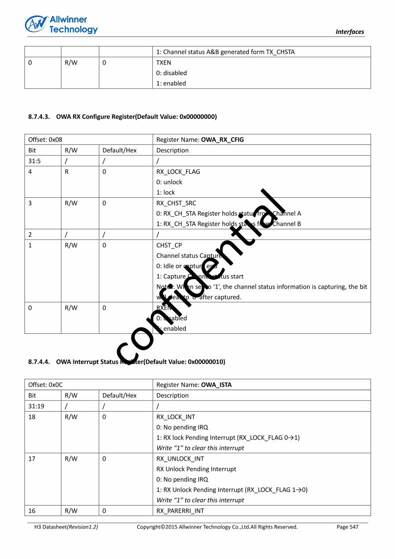
Interfaces
H3 Datasheet(Revision1.2) Copyright© 2015 Allwinner Technology Co.,Ltd.All Rights Reserved. Page 547
1: Channel status A&B generated form TX_CHSTA
0 R/W 0 TXEN
0: disabled
1: enabled
8.7.4.3. OWA RX Configure Register(Default Value: 0x00000000)
Offset: 0x08 Register Name: OWA_RX_CFIG
Bit R/W Default/Hex Description
31:5 / / /
4 R 0 RX_LOCK_FLAG
0: unlock
1: lock
3 R/W 0 RX_CHST_SRC
0: RX_CH_STA Register holds status from Channel A
1: RX_CH_STA Register holds status from Channel B
2 / / /
1 R/W 0 CHST_CP
Channel status Capture
0: Idle or capture end
1: Capture Channel status start
Notes: When set to ‘1’, the channel status information is capturing, the bit
will clear to ‘0’ after captured.
0 R/W 0 RXEN
0: disabled
1: enabled
8.7.4.4. OWA Interrupt Status Register(Default Value: 0x00000010)
Offset: 0x0C Register Name: OWA_ISTA
Bit R/W Default/Hex Description
31:19 / / /
18 R/W 0 RX_LOCK_INT
0: No pending IRQ
1: RX lock Pending Interrupt (RX_LOCK_FLAG 0→1)
Write “1” to clear this interrupt
17 R/W 0 RX_UNLOCK_INT
RX Unlock Pending Interrupt
0: No pending IRQ
1: RX Unlock Pending Interrupt (RX_LOCK_FLAG 1→0)
Write “1” to clear this interrupt
16 R/W 0 RX_PARERRI_INT
confid
ential
Interfaces
H3 Datasheet(Revision1.2) Copyright© 2015 Allwinner Technology Co.,Ltd.All Rights Reserved. Page 548
RX Parity Error Pending Interrupt
0: No pending IRQ
1: RX Parity Error Pending Interrupt
Write “1” to clear this interrupt
15:7 / / /
6 R/W 0 TXU_INT
TX FIFO Under run Pending Interrupt
0: No pending IRQ
1: FIFO Under run Pending Interrupt
Write “1” to clear this interrupt
5 R/W 0 TXO_INT
TX FIFO Overrun Pending Interrupt
0: No Pending IRQ
1: FIFO Overrun Pending Interrupt
Write “1” to clear this interrupt
4 R/W 1 TXE_INT
TX FIFO Empty Pending Interrupt
0: No Pending IRQ
1: FIFO Empty Pending Interrupt
Write “1” to clear this interrupt or automatically clear if interrupt condition
fails.
3:2 / / /
1 R/W 0 RXO_INT
RX FIFO Overrun Pending Interrupt
0: FIFO Overrun Pending
Write “1” to clear this interrupt
0 R/W 0 RXA_INT
RX FIFO Available Pending Interrupt
0: No Pending IRQ
1: Data Available Pending IRQ
Write “1” to clear this interrupt or automatically clear if interrupt condition
fails
8.7.4.5. OWA RX FIFO Register(Default Value: 0x00000000)
Offset: 0x10 Register Name: OWA_RXFIFO
Bit R/W Default/Hex Description
31:0 R 0 RX_DATA
Host can get one sample by reading this register, the A channel data is first
and then the B channel data
confid
ential

Interfaces
H3 Datasheet(Revision1.2) Copyright© 2015 Allwinner Technology Co.,Ltd.All Rights Reserved. Page 549
8.7.4.6. OWA FIFO Control Register(Default Value: 0x00001078)
Offset: 0x14 Register Name: OWA_FCTL
Bit R/W Default/Hex Description
31 R/W 0 HUB_EN
Audio hub enable
0 : Disable
1: Enable
30:18 / / /
17 R/W 0 FTX
Write “1” to flush TX FIFO, self clear to “0”
16 R/W 0 FRX
Write “1” to flush RX FIFO, self clear to “0”
15:13 / / /
12:8 R/W 0x10 TXTL
TX FIFO empty Trigger Level
Interrupt and DMA request trigger level for TX FIFO normal condition
Trigger Level = TXTL
7:3 R/W 0x0F RXTL
RX FIFO Trigger Level
Interrupt and DMA request trigger level for RX FIFO normal condition
Trigger Level = RXTL + 1
2 R/W 0 TXIM
TX FIFO Input Mode(Mode0, 1)
0: Valid data at the MSB of OWA_TXFIFO register
1: Valid data at the LSB of OWA_TXFIFO register
Example for 20-bits transmitted audio sample:
Mode 0: FIFO_I[23:0] = {TXFIFO[31:12], 4’h0}
Mode 1: FIFO_I[23:0] = {TXFIFO[19:0], 4’h0}
1:0 R/W 0 RXOM
RX FIFO Output Mode(Mode 0,1,2,3)
00: Expanding “0” at LSB of SPDIP_RXFIFO register
01: Expanding received sample sign bit at MSB of OWA_RXFIFO register
10: Truncating received samples at high half-word of OWA_RXFIFO register
and low half-word of AC_FIFO register is filled by “0”
11: Truncating received samples at low half-word of OWA_RXFIFO register
and high half-word of AC_FIFO register is expanded by its sigh bit
Mode0: RXFIFO[31:0] = {FIFO_O[23:0], 8’h0}
Mode 1: RXFIFO[31:0] = {8’FIFO_O[23], FIFO_O[23:0]}
Mode 2: RXFIFO[31:0] = {FIFO_O[23:8], 16’h0}
Mode 3: RXFIFO[31:0] = {16’FIFO_O[23], FIFO_O[23:8]}
confid
ential

Interfaces
H3 Datasheet(Revision1.2) Copyright© 2015 Allwinner Technology Co.,Ltd.All Rights Reserved. Page 550
8.7.4.7. OWA FIFO Status Register(Default Value: 0x00006000)
Offset: 0x18 Register Name: OWA_FSTA
Bit R/W Default/Hex Description
31:15 / / /
14 R 1 TXE
TX FIFO Empty (indicate FIFO is not full)
0: No room for new sample in TX FIFO
1: More than one room for new sample in TX FIFO ( >=1 word )
13:8 R 0x20 TXE_CNT
TX FIFO Empty Space Word counter
7 / / /
6 R 0 RXA
RX FIFO Available
0: No available data in RX FIFO
1: More than one sample in RX FIFO ( >=1 word )
5:0 R 0 RXA_CNT
RX FIFO Available Sample Word counter
8.7.4.8. OWA Interrupt Control Register(Default Value: 0x00000000)
Offset: 0x1C Register Name: OWA_INT
Bit R/W Default/Hex Description
31:19 / / /
18 R/W 0 RX_LOCKI_EN
RX LOCK Interrupt enable
0: Disable
1: Enable
17 R/W 0 RX_UNLOCKI_EN
RX UNLOCK Interrupt enable
0: Disable
1: Enable
16 R/W 0 RX_PARERRI_EN
RX PARITY ERORR Interrupt enable
0: Disable
1: Enable
15:8 / / /
7 R/W 0 TX_DRQ
TX FIFO Empty DRQ Enable
0: Disable
1: Enable
6 R/W 0 TXUI_EN
TX FIFO Under run Interrupt Enable
confid
ential
Interfaces
H3 Datasheet(Revision1.2) Copyright© 2015 Allwinner Technology Co.,Ltd.All Rights Reserved. Page 551
0: Disable
1: Enable
5 R/W 0 TXOI_EN
TX FIFO Overrun Interrupt Enable
0: Disable
1: Enable
4 R/W 0 TXEI_EN
TX FIFO Empty Interrupt Enable
0: Disable
1: Enable
3 / / /
2 R/W 0 RX_DRQ
RX FIFO Data Available DRQ Enable
When set to “1”, RX FIFO DMA Request is asserted if Data is available in RX
FIFO
0: Disable
1: Enable
1 R/W 0 RXOI_EN
RX FIFO Overrun Interrupt Enable
0: Disable
1: Enable
0 R/W 0 RXAI_EN
RX FIFO Data Available Interrupt Enable
0: Disable
1: Enable
8.7.4.9. OWA TX FIFO Register(Default Value: 0x00000000)
Offset: 0x20 Register Name: OWA_TXFIFO
Bit R/W Default/Hex Description
31:0 W 0 TX_DATA
Transmitting A, B channel data should be written this register one by one.
The A channel data is first and then the B channel data.
8.7.4.10. OWA TX Counter Register(Default Value: 0x00000000)
Offset: 0x24 Register Name: OWA_TX_CNT
Bit R/W Default/Hex Description
31:0 R/W 0 TX_CNT
TX Sample counter
The audio sample number of writing into TX FIFO. When one sample is
written by DMA or by host IO, the TX sample counter register increases by
confid
ential
Interfaces
H3 Datasheet(Revision1.2) Copyright© 2015 Allwinner Technology Co.,Ltd.All Rights Reserved. Page 552
one. The TX Counter register can be set to any initial value at any time.
After been updated by the initial value, the counter register should count
on base of this value.
8.7.4.11. OWA RX Counter Register(Default Value: 0x00000000)
Offset: 0x28 Register Name: OWA_RX_CNT
Bit R/W Default/Hex Description
31:0 R/W 0 RX_CNT
RX Sample counter
The audio sample number of writing into RX FIFO. When one sample is
written by Codec, the RX sample counter register increases by one. The RX
Counter register can be set to any initial value at any time. After been
updated by the initial value, the counter register should count on base of
this value.
8.7.4.12. OWA TX Channel Status Register0(Default Value: 0x00000000)
Offset: 0x2C Register Name: OWA_TX_CHSTA0
Bit R/W Default/Hex Description
31: 30 / / /
29:28 R/W CA
Clock Accuracy
00: Level 2
01: Level 1
10: Level 3
11: not matched
27:24 R/W FREQ
Sampling frequency
0000: 44.1kHz 1000: Reserved
0001: not indicated 1001: 768kHz
0010: 48kHz 1010: 96kHz
0011: 32kHz 1011: Reserved
0100: 22.05kHz 1100:176.4kHz
0101: Reserved 1101: Reserved
0110: 24kHz 1110: 192kHz
0111: Reserved 1111: Reserved
23:20 R/W 0 CN
Channel Number
19:16 R/W 0 SN
Source Number
15:8 R/W 0 CC
confid
ential

Interfaces
H3 Datasheet(Revision1.2) Copyright© 2015 Allwinner Technology Co.,Ltd.All Rights Reserved. Page 553
Category code
Indicates the kind of equipment that generates the digital audio
interface signal.
7:6 R/W 0 MODE
Mode
00: Default Mode
01~11: Reserved
5:3 R/W 0 EMP
Emphasis
Additional format information
For bit 1 = “0”, Linear PCM audio mode:
000: 2 audio channels without pre-emphasis
001: 2 audio channels with 50 μs / 15 μs pre-emphasis
010: Reserved (for 2 audio channels with pre-emphasis)
011: Reserved (for 2 audio channels with pre-emphasis)
100~111: Reserved
For bit 1 = “1”, other than Linear PCM applications:
000: Default state
001~111: Reserved
2 R/W 0 CP
Copyright
0: copyright is asserted
1: no copyright is asserted
1 R/W 0 TYPE
Audio Data Type
0: Linear PCM Samples
1: For none-linear PCM audio such as AC3, DTS, MPEG audio
0 R/W 0 PRO
Application type
0: Consumer Application
1: Professional Application
Note: This bit must be fixed to “0”
8.7.4.13. OWA TX Channel Status Register1(Default Value: 0x00000000)
Offset: 0x30 Register Name: OWA_TX_CHSTA1
Bit R/W Default/Hex Description
31:10 / / /
9:8 R/W 0 CGMS_A
00: Copying is permitted without restriction
01: One generation of copies may be made
10: Condition not be used
11: No copying is permitted
7:4 R/W 0 ORIG_FREQ
confid
ential

Interfaces
H3 Datasheet(Revision1.2) Copyright© 2015 Allwinner Technology Co.,Ltd.All Rights Reserved. Page 554
Original sampling frequency
0000: not indicated
0001: 192kHz
0010: 12kHz
0011: 176.4kHz
0100: Reserved
0101: 96kHz
0110: 8kHz
0111: 88.2kHz
1000: 16kHz
1001: 24kHz
1010: 11.025kHz
1011: 22.05kHz
1100: 32kHz
1101: 48kHz
1110: Reserved
1111: 44.1kHz
3:1 R/W 0 WL
Sample word length
For bit 0 = “0”:
000: not indicated
001: 16 bits
010: 18 bits
100: 19 bits
101: 20 bits
110: 17 bits
111: Reserved
For bit 0 = “1”:
000: not indicated
001: 20 bits
010: 22 bits
100: 23 bits
101: 24 bits
110: 21 bits
111: Reserved
0 R/W 0 MWL
Max Word length
0: Maximum audio sample word length is 20 bits
1: Maximum audio sample word length is 24 bits
8.7.4.14. OWA RX Channel Status Register0(Default Value: 0x00000000)
Offset: 0x34 Register Name: OWA_RX_CHSTA0
confid
ential

Interfaces
H3 Datasheet(Revision1.2) Copyright© 2015 Allwinner Technology Co.,Ltd.All Rights Reserved. Page 555
Bit R/W Default/Hex Description
31: 30 / / /
29:28 R/W CA
Clock Accuracy
00: Level 2
01: Level 1
10: Level 3
11: not matched
27:24 R/W FREQ
Sampling frequency
0000: 44.1kHz 1000: Reserved
0001: not indicated 1001: 768kHz
0010: 48kHz 1010: 96kHz
0011: 32kHz 1011: Reserved
0100: 22.05kHz 1100:176.4kHz
0101: Reserved 1101: Reserved
0110: 24kHz 1110: 192kHz
0111: Reserved 1111: Reserved
23:20 R/W 0 CN
Channel Number
19:16 R/W 0 SN
Source Number
15:8 R/W 0 CC
Category code
Indicates the kind of equipment that generates the digital audio interface
signal.
7:6 R/W 0 MODE
Mode
00: Default Mode
01~11: Reserved
5:3 R/W 0 EMP
Emphasis
Additional format information
For bit 1 = “0”, Linear PCM audio mode:
000: 2 audio channels without pre-emphasis
001: 2 audio channels with 50 μs / 15 μs pre-emphasis
010: Reserved (for 2 audio channels with pre-emphasis)
011: Reserved (for 2 audio channels with pre-emphasis)
100~111: Reserved
For bit 1 = “1”, other than Linear PCM applications:
000: Default state
001~111: Reserved
2 R/W 0 CP
Copyright
0: copyright is asserted
confid
ential

Interfaces
H3 Datasheet(Revision1.2) Copyright© 2015 Allwinner Technology Co.,Ltd.All Rights Reserved. Page 556
1: no copyright is asserted
1 R/W 0 TYPE
Audio Data Type
0: Linear PCM Samples
1: For none-linear PCM audio such as AC3, DTS, MPEG audio
0 R/W 0 PRO
Application type
0: Consumer Application
1: Professional Application
8.7.4.15. OWA RX Channel Status Register1(Default Value: 0x00000000)
Offset: 0x38 Register Name: OWA_CH_STA0
Bit R/W Default/Hex Description
31:10 / / /
9:8 R/W 0 CGMS_A
00: Copying is permitted without restriction
01: One generation of copies may be made
10: Condition not be used
11: No copying is permitted
7:4 R/W 0 ORIG_FREQ
Original sampling frequency
0000: not indicated
0001: 192kHz
0010: 12kHz
0011: 176.4kHz
0100: Reserved
0101: 96kHz
0110: 8kHz
0111: 88.2kHz
1000: 16kHz
1001: 24kHz
1010: 11.025kHz
1011: 22.05kHz
1100: 32kHz
1101: 48kHz
1110: Reserved
1111: 44.1kHz
3:1 R/W 0 WL
Sample word length
For bit 0 = “0”:
000: not indicated
001: 16 bits
010: 18 bits
confid
ential

Interfaces
H3 Datasheet(Revision1.2) Copyright© 2015 Allwinner Technology Co.,Ltd.All Rights Reserved. Page 557
100: 19 bits
101: 20 bits
110: 17 bits
111: Reserved
For bit 0 = “1”:
000: not indicated
001: 20 bits
010: 22 bits
100: 23 bits
101: 24 bits
110: 21 bits
111: Reserved
0 R/W 0 MWL
Max Word length
0: Maximum audio sample word length is 20 bits
1: Maximum audio sample word length is 24 bits
confid
ential

Interfaces
H3 Datasheet(Revision1.2) Copyright© 2015 Allwinner Technology Co.,Ltd.All Rights Reserved. Page 558
8.8. SCR
8.8.1. Overview
The Smart Card Reader (SCR) is a communication controller that transmits data between the system and Smart Card.
The controller can perform a complete smart card session, including card activation, card deactivation. Cold/warm reset,
Answer to Reset (ATR) response reception, data transfers, etc.
The SCR includes the following features:
Supports APB slave interface for easy integration with AMBA-based host systems
Supports the ISO/IEC 7816-3:1997(E) and EMV2000 (4.0) Specifications
Performs functions needed for complete smart card sessions, including:
- Card activation and deactivation
- Cold/warm reset
- Answer to Reset (ATR) response reception
- Data transfers to and from the card
Supports adjustable clock rate and bit rate
Configurable automatic byte repetition
Support commonly used communication protocols:
- T=0 for asynchronous half-duplex character transmission
- T=1 for asynchronous half-duplex block transmission
Support FIFOs for receive and transmit buffers (up to 128 characters) with threshold
Support configurable timing functions:
- Smart card activation time
- Smart card reset time
- Guard time
- Timeout timers
Supports synchronous and any other non-ISO 7816 and non-EMV cards
8.8.2. Block Diagram
The Top Diagram of Smart Card Reader is below:
confid
ential
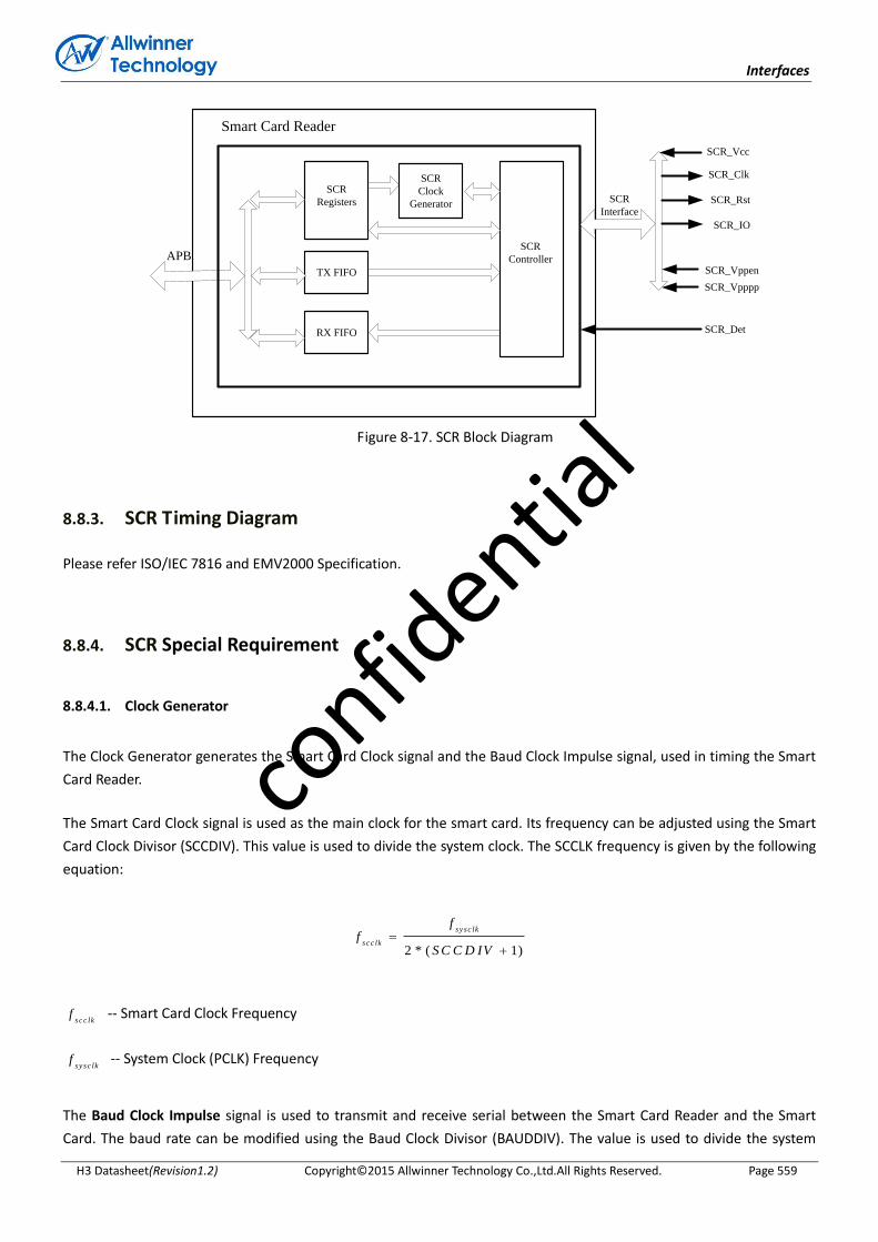
Interfaces
H3 Datasheet(Revision1.2) Copyright© 2015 Allwinner Technology Co.,Ltd.All Rights Reserved. Page 559
Smart Card Reader
APB
SCR
Registers
TX FIFO
RX FIFO
SCR
Clock
Generator
SCR
Controller
SCR
Interface
SCR_Det
SCR_Vpppp
SCR_Vppen
SCR_Vcc
SCR_Clk
SCR_Rst
SCR_IO
Figure 8-17. SCR Block Diagram
8.8.3. SCR Timing Diagram
Please refer ISO/IEC 7816 and EMV2000 Specification.
8.8.4. SCR Special Requirement
8.8.4.1. Clock Generator
The Clock Generator generates the Smart Card Clock signal and the Baud Clock Impulse signal, used in timing the Smart
Card Reader.
The Smart Card Clock signal is used as the main clock for the smart card. Its frequency can be adjusted using the Smart
Card Clock Divisor (SCCDIV). This value is used to divide the system clock. The SCCLK frequency is given by the following
equation:
2 * ( 1)
sysc lk
scc lk
ff
S C C D IV
sc c lkf -- Smart Card Clock Frequency
sysc lkf -- System Clock (PCLK) Frequency
The Baud Clock Impulse signal is used to transmit and receive serial between the Smart Card Reader and the Smart
Card. The baud rate can be modified using the Baud Clock Divisor (BAUDDIV). The value is used to divide the system
confid
ential
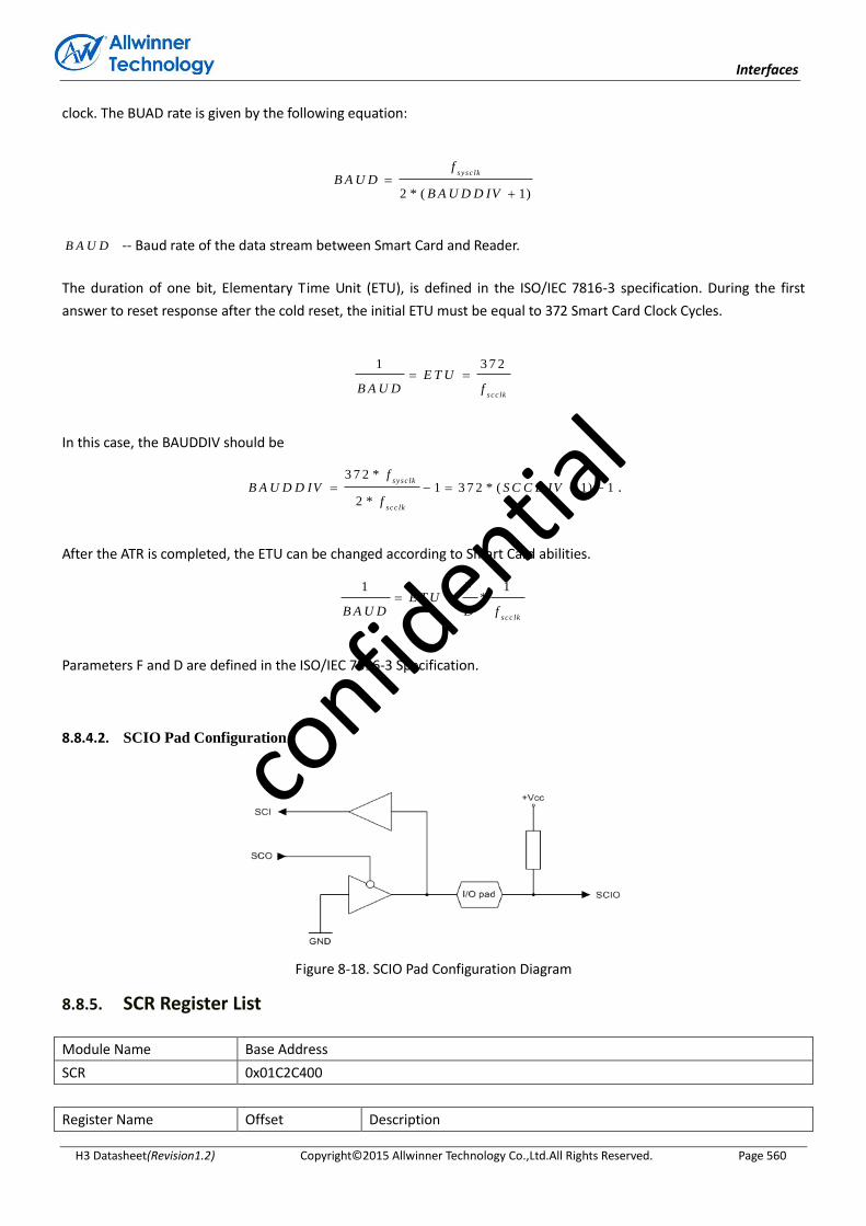
Interfaces
H3 Datasheet(Revision1.2) Copyright© 2015 Allwinner Technology Co.,Ltd.All Rights Reserved. Page 560
clock. The BUAD rate is given by the following equation:
2 * ( 1)
sysc lkf
B A U DB A U D D IV
B A U D -- Baud rate of the data stream between Smart Card and Reader.
The duration of one bit, Elementary Time Unit (ETU), is defined in the ISO/IEC 7816-3 specification. During the first
answer to reset response after the cold reset, the initial ETU must be equal to 372 Smart Card Clock Cycles.
1 3 7 2
scc lk
E T UB A U D f
In this case, the BAUDDIV should be
3 7 2 *1 3 7 2 * ( 1) 1
2 *
sy sc lk
sc c lk
fB A U D D IV S C C D IV
f .
After the ATR is completed, the ETU can be changed according to Smart Card abilities.
1 1*
scc lk
FE T U
B A U D D f
Parameters F and D are defined in the ISO/IEC 7816-3 Specification.
8.8.4.2. SCIO Pad Configuration
Figure 8-18. SCIO Pad Configuration Diagram
8.8.5. SCR Register List
Module Name Base Address
SCR 0x01C2C400
Register Name Offset Description
confid
ential

Interfaces
H3 Datasheet(Revision1.2) Copyright© 2015 Allwinner Technology Co.,Ltd.All Rights Reserved. Page 561
SCR_CSR 0x000 Smart Card Reader Control and Status Register
SCR_INTEN 0x004 Smart Card Reader Interrupt Enable Register 1
SCR_INTST 0x008 Smart Card Reader Interrupt Status Register 1
SCR_FCSR 0x00c Smart Card Reader FIFO Control and Status Register
SCR_FCNT 0x010 Smart Card Reader RX and TX FIFO Counter Register
SCR_RPT 0x014 Smart Card Reader RX and TX Repeat Register
SCR_DIV 0x018 Smart Card Reader Clock and Baud Divisor Register
SCR_LTIM 0x01c Smart Card Reader Line Time Register
SCR_CTIM 0x020 Smart Card Reader Character Time Register
SCR_LCTLR 0x030 Smart Card Reader Line Control Register
SCR_FIFO 0x100 Smart Card Reader RX and TX FIFO Access Point
8.8.6. SCR Register Description
8.8.6.1. Smart Card Reader Control and Status Register(Default Value: 0x00000000)
Offset: 0x00 Register Name: SCR_CSR
Bit R/W Default/Hex Description
31 R 0
SCDET
Smart Card Detected
This bit is set to ‘1’ when the scdetect input is active at least for a
debounce time.
30 / / /
24 R/W 0
SCDETPOL
Smart Card Detect Polarity
This bit set polarity of scdetect signal.
0: Low Active
1: High Active
23:22 R/W 0
Protocol Selection (PTLSEL)
0x0 – T=0.
0x1 – T=1, no character repeating and no guard time is used when T=1
protocol is selected.
0x2 – Reserved
0x3 – Reserved
21 R/W 0
ATRSTFLUSH
ATR Start Flush FIFO
When enabled, both FIFOs are flushed before the ATR is started.
20 R/W 0
TSRXE
TS Receive Enable
When set to ‘1’, the TS character (the first ATR character) will be store in
RXFIFO during card session.
19 R/W 0 CLKSTPPOL
confid
ential
Interfaces
H3 Datasheet(Revision1.2) Copyright© 2015 Allwinner Technology Co.,Ltd.All Rights Reserved. Page 562
Clock Stop Polarity
The value of the scclk output during the clock stop state.
18 R/W 0
PECRXE
Parity Error Character Receive Enable
Enables storage of the characters received with wrong parity in RX FIFO.
17 R/W 0
MSBF
MSB First
When high, inverse bit ordering convention (msb to lsb) is used.
16 R/W 0
DATAPOL
Data Plorarity
When high, inverse level convention is used (A=’1’, Z=’0’).
15:12 / / /
11 R/W 0
DEACTDeactivation. Setting of this bit initializes the deactivation sequence.
When the deactivation is finished, the DEACT bit is automatically cleared.
10 R/W 0
ACT
Activation. Setting of this bit initializes the activation sequence. When the
activation is finished, the ACT bit is automatically cleared.
9 R/W 0
WARMRST
Warm Reset Command. Writing ‘1’ to this bit initializes Warm Reset of the
Smart Card. This bit is always read as ‘0’.
8 R/W 0
CLKSTOP
Clock Stop. When this bit is asserted and the smart card I/O line is in ‘Z’
state, the SCR core stops driving of the smart card clock signal after the
CLKSTOPDELAY time expires. The smart card clock is restarted immediately
after the CLKSTOP signal is deasserted. New character transmission can be
started after CLKSTARTDELAY time. The expiration of both times is signaled
by the CLKSTOPRUN bit in the interrupt registers.
7:3 / / Reserved
2 R/W 0
GINTEN
Global Interrupt Enable. When high, IRQ output assertion is enabled.
1 R/W 0
RXEN
Receiving Enable. When enabled the characters sent by the Smart Card are
received by the UART and stored in RX FIFO. Receiving is internally disabled
while a transmission is in progress.
0 R/W 0
TXEN
Transmission Enable. When enabled the characters are read from TX FIFO
and transmitted through UART to the Smart Card.
8.8.6.2. Smart Card Reader Interrupt Enable Register(Default Value: 0x00000000)
Offset: 0x04 Register Name: SCR_INTEN
Bit R/W Default/Hex Description
31:24 / / /
confid
ential

Interfaces
H3 Datasheet(Revision1.2) Copyright© 2015 Allwinner Technology Co.,Ltd.All Rights Reserved. Page 563
23 R/W 0
SCDEA
Smart Card Deactivation Interrupt Enable.
22 R/W 0
SCACT
Smart Card Activation Interrupt Enable.
21 R/W 0
SCINS
Smart Card Inserted Interrupt Enable.
20 R/W 0
SCREM
Smart Card Removed Interrupt Enable.
19 R/W 0
ATRDONE
ATR Done Interrupt Enable.
18 R/W 0
ATRFAIL
ATR Fail Interrupt Enable.
17 R/W 0
C2CFULL
Two Consecutive Characters Limit Interrupt Enable.
16 R/W 0
CLKSTOPRUN
Smart Card Clock Stop/Run Interrupt Enable.
15:13 / / /
12 R/W 0
RXPERR
RX Parity Error Interrupt Enable.
11 R/W 0
RXDONE
RX Done Interrupt Enable.
10 R/W 0
RXFIFOTHD
RX FIFO Threshold Interrupt Enable.
9 R/W 0
RXFIFOFULL
RX FIFO Full Interrupt Enable.
8 / / /
7:5 / / /
4 R/W 0
TXPERR
TX Parity Error Interrupt Enable.
3 R/W 0
TXDONE
TX Done Interrupt Enable.
2 R/W 0
TXFIFOTHD
TX FIFO Threshold Interrupt Enable.
1 R/W 0
TXFIFOEMPTY
TX FIFO Empty Interrupt Enable.
0 R/W 0
TXFIFODONE
TX FIFO Done Interrupt Enable.
8.8.6.3. Smart Card Reader Interrupt Status Register(Default Value: 0x00000000)
Offset: 0x08 Register Name: SCR_INTST
Bit R/W Default/Hex Description
31:24 / / /
confid
ential

Interfaces
H3 Datasheet(Revision1.2) Copyright© 2015 Allwinner Technology Co.,Ltd.All Rights Reserved. Page 564
23 R/W 0
SCDEA
Smart Card Deactivation Interrupt. When enabled, this interrupt is asserted
after the Smart Card deactivation sequence is complete.
22 R/W 0
SCACT
Smart Card Activation Interrupt. When enabled, this interrupt is asserted
after the Smart Card activation sequence is complete.
21 R/W 0
SCINS
Smart Card Inserted Interrupt. When enabled, this interrupt is asserted
after the smart card insertion.
20 R/W 0
SCREM
Smart Card Removed Interrupt. When enabled, this interrupt is asserted
after the smart card removal.
19 R/W 0
ATRDONE
ATR Done Interrupt. When enabled, this interrupt is asserted after the ATR
sequence is successfully completed.
18 R/W 0
ATRFAIL
ATR Fail Interrupt. When enabled, this interrupt is asserted if the ATR
sequence fails.
17 R/W 0
C2CFULL
Two Consecutive Characters Limit Interrupt. When enabled, this interrupt
is asserted if the time between two consecutive characters, transmitted
between the Smart Card and the Reader in both directions, is equal the
Two Characters Delay Limit described below. The C2CFULL interrupt is
internally enabled from the ATR start to the deactivation or ATR restart
initialization. It is recommended to use this counter to detect unresponsive
Smart Cards.
16 R/W 0
CLKSTOPRUN
Smart Card Clock Stop/Run Interrupt. When enabled, this interrupt is
asserted in two cases:
When the smart card clock is stopped.
When the new character can be started after the clock restart.
To distinguish between the two interrupt cases, we recommend reading
the CLKSTOP bit in SCR_CTRL1 register.
15:13 / / /
12 R/W 0
RXPERR
RX Parity Error Interrupt. When enabled, this interrupt is asserted after the
character with wrong parity was received when the number of repeated
receptions exceeds RXREPEAT value or T=1 protocol is used.
11 R/W 0
RXDONE
RX Done Interrupt. When enabled, this interrupt is asserted after a
character was received from the Smart Card.
10 R/W 0
RXFIFOTHD
RX FIFO Threshold Interrupt. When enabled, this interrupt is asserted if the
number of bytes in RX FIFO is equal or exceeds the RX FIFO threshold.
9 R/W 0 RXFIFOFULL
confid
ential
Interfaces
H3 Datasheet(Revision1.2) Copyright© 2015 Allwinner Technology Co.,Ltd.All Rights Reserved. Page 565
RX FIFO Full Interrupt. When enabled, this interrupt is asserted if the RX
FIFO is filled up.
8 / / /
7:5 / / /
4 R/W 0
TXPERR
TX Parity Error Interrupt. When enabled, this interrupt is asserted if the
Smart Card signals wrong character parity during the guard time after the
character transmission was repeated TXREPEAT times or T=1 protocol is
used.
3 R/W 0
TXDONE
TX Done Interrupt. When enabled, this interrupt is asserted after one
character was transmitted to the smart card.
2 R/W 0
TXFIFOTHD
TX FIFO Threshold Interrupt. When enabled, this interrupt is asserted if the
number of bytes in TX FIFO is equal or less than the TX FIFO threshold.
1 R/W 0
TXFIFOEMPTY
TX FIFO Empty Interrupt. When enabled, this interrupt is asserted if the TX
FIFO is emptied out.
0 R/W 0
TXFIFODONE
TX FIFO Done Interrupt. When enabled, this interrupt is asserted after all
bytes from TX FIFO ware transferred to the Smart Card.
Note: This register provides information about the state of each interrupt bit. You can clear the register bits individually
by writing ‘1’ to a bit you intend to clear.
8.8.6.4. Smart Card Reader FIFO Control and Status Register(Default Value: 0x00000000)
Offset: 0x0C Register Name: SCR_FCSR
Bit R/W Default/Hex Description
31:11 / / /
10 R/W 0
RXFIFOFLUSH
Flush RX FIFO. RX FIFO is flushed, when ‘1’ is written to this bit.
9 R 0
RXFIFOFULL
RX FIFO Full.
8 R 1
RXFIFOEMPTY
RX FIFO Empty.
7:3 / / /
2 R/W 0
TXFIFOFLUSH
Flush TX FIFO. TX FIFO is flushed, when ‘1’ is written to this bit.
1 R 0
TXFIFOFULL
TX FIFO Full.
0 R 1
TXFIFOEMPTY
TX FIFO Empty.
confid
ential
Interfaces
H3 Datasheet(Revision1.2) Copyright© 2015 Allwinner Technology Co.,Ltd.All Rights Reserved. Page 566
8.8.6.5. Smart Card Reader FIFO Counter Register(Default Value: 0x00000000)
Offset: 0x10 Register Name: SCR_FIFOCNT
Bit R/W Default/Hex Description
31:24 R/W 0
RXFTH
RX FIFO Threshold
These bits set the interrupt threshold of RX FIFO. The interrupt is asserted
when the number of bytes it receives is equal to, or exceeds the threshold.
23:16 R/W 0
TXFTH
TX FIFO Threshold
These bits set the interrupt threshold of TX FIFO. The interrupt is asserted
when the number of bytes in TX FIFO is equal to or less than the threshold.
15:8 R 0
RXFCNT
RX FIFO Counter
These bits provide the number of bytes stored in the RXFIFO.
7:0 R 0
TXFCNT
TX FIFO Counter
These bits provide the number of bytes stored in the TXFIFO.
8.8.6.6. Smart Card Reader Repeat Control Register(Default Value: 0x00000000)
Offset: 0x14 Register Name: SCR_REPEAT
Bit R/W Default/Hex Description
31:8 / / /
7:4 R/W 0
RXRPT
RX Repeat
This is a 4-bit register that specifies the number of attempts to request
character re-transmission after wrong parity was detected. The
re-transmission of the character is requested using the error signal during
the guard time.
3:0 R/W 0
TXRPT
TX Repeat
This is a 4-bit register that specifies the number of attempts to re-transmit
the character after the Smart Card signals the wrong parity during the
guard time.
8.8.6.7. Smart Card Reader Clock Divisor Register(Default Value: 0x00000000)
Offset: 0x18 Register Name: SCR_CLKDIV
Bit R/W Default/Hex Description
31:16 R/W 0
BAUDDIV
Baud Clock Divisor. This 16-bit register defines the divisor value used to
confid
ential
Interfaces
H3 Datasheet(Revision1.2) Copyright© 2015 Allwinner Technology Co.,Ltd.All Rights Reserved. Page 567
generate the Baud Clock impulses from the system clock.
2 * ( 1)
sysc lkf
B A U DB A U D D IV
15:0 R/W 0
SCCDIV
Smart Card Clock Divisor. This 16-bit register defines the divisor value used
to generate the Smart Card Clock from the system clock.
2 * ( 1)
sysc lk
scc lk
ff
S C C D IV
scc lkf
is the frequency of Smart Card Clock Signal.
s y s c lkf
is the frequency of APB Clock.
8.8.6.8. Smart Card Reader Line Time Register(Default Value: 0x00000000)
Offset: 0x1C Register Name: SCR_LTIM
Bit R/W Default/Hex Description
31:24 / / /
23:16 R/W 0
ATR
ATR Start Limit. This 16-bit register defines the maximum time between the
rising edge of the scrstn signal and the start of ATR response.
ATR Start Limit = 128* ATR* scc lkT
.
15:8 R/W 0
RST
Reset Duration. This 16-bit register sets the duration of the Smart Card
reset sequence. This value is same for the cold and warm reset.
Cold/Warm Reset Duration = 128* RST* scc lkT
.
7:0 R/W 0
ACT
Activation/Deactivation Time. This 16-bit register sets the duration of each
part of the activation and deactivation sequence.
Activation/Deactivation Duration = 128* ACT * scc lkT
.
1
s c c lk
s c c lk
Tf
is the Smart Card Clock Cycle.
8.8.6.9. Smart Card Reader Character Time Register(Default Value: 0x00000000)
Offset: 0x20 Register Name: SCR_CTIM
confid
ential

Interfaces
H3 Datasheet(Revision1.2) Copyright© 2015 Allwinner Technology Co.,Ltd.All Rights Reserved. Page 568
Bit R/W Default/Hex Description
31:16 R/W 0
CHARLIMIT
Character Limit. This 16-bit register sets the maximum time between the
leading edges of two consecutive characters. The value is ETUs.
15:8 / / /
7:0 R/W 0
GUARDTIME
Character Guard time. This 8-bit register sets a delay at the end of each
character transmitted from the Smart Card Reader to the Smart Card. The
value is in ETUs. The parity error is besides signaled during the guard time.
8.8.6.10. Smart Card Reader Line Control Register(Default Value: 0x00000000)
Offset: 0x30 Register Name: SCR_PAD
Bit R/W Default/Hex Description
31:8 / / /
7 R/W 0
DSCVPPPP
Direct Smart Card Vpp Pause/Prog. It provides direct access to SCVPPPP
output.
6 R/W 0
DSCVPPEN
Direct Smart Card Vpp Enable. It provides direct access to SCVPPEN output.
5 R/W 0
AUTOADEAVPP
Automatic Vpp Handling. When high, it enables automatic handling of
DSVPPEN and DSVPPPP signals during activation and deactivation
sequence.
4 R/W 0
DSCVCC
Direct Smart Card VCC. When DIRACCPADS=’1’, the DSCVCC bit provides
direct access to SCVCC pad.
3 R/W 0
DSCRST
Direct Smart Card Clock. When DIRACCPADS=’1’, the DSCRST bit provides
direct access to SCRST pad.
2 R/W 0
DSCCLK
Direct Smart Card Clock. When DIRACCPADS=’1’, the DSCCLK bit provides
direct access to SCCLK pad.
1 R/W 0
DSCIO
Direct Smart Card Input/Output. When DIRACCPADS=’1’, the DSCIO bit
provides direct access to SCIO pad.
0 R/W 0
DIRACCPADS
Direct Access to Smart Card Pads. When high, it disables a serial interface
functionality and enables direct control of the smart card pads using
following 4 bits.
Note: This register provides direct access to smart card pads without serial interface assistance. You can use this register
feature with synchronous and any other non-ISO 7816 and non-EMV cards.
confid
ential
Interfaces
H3 Datasheet(Revision1.2) Copyright© 2015 Allwinner Technology Co.,Ltd.All Rights Reserved. Page 569
8.8.6.11. Smart Card Reader FIFO Data Register(Default Value: 0x00000000)
Offset: 0x0100 Register Name: SCR_FIFO
Bit R/W Default/Hex Description
31:8 / / /
7:0 R/W 0
FIFO_DATA
This 8-bit register provides access to the RX and TX FIFO buffers. The TX
FIFO is accessed during the APB write transfer. The RX FIFO is accessed
during the APB read transfer.
confid
ential
Interfaces
H3 Datasheet(Revision1.2) Copyright© 2015 Allwinner Technology Co.,Ltd.All Rights Reserved. Page 570
8.9. EMAC
8.9.1. Overview
The Ethernet MAC(EMAC) controller enables a host to transmit and receive data over Ethernet in compliance with
the IEEE 802.3-2002 standard. It supports 10M/100M/1000M external PHY with MII/ RGMII interface in both full
and half duplex mode. The Ethernet MAC-DMA is designed for packet-oriented data transfers based on a linked list
of descriptors. 4K Byte TXFIFO and 16K Byte RXFIFO are provided to keep continuous transmission and reception.
Flow Control, CRC Pad & Stripping, and address filtering are also supported in this module.
The Ethernet MAC Controller includes the following features:
Supports 10/100/1000Mbps data transfer rates
Supports MII/RGMII PHY interface
Supports both full-duplex and half-duplex operation
Programmable frame length to support Standard or Jumbo Ethernet frames with sizes up to 16 KB
Supports a variety of flexible address filtering modes
Separate 32-bit status returned for transmission and reception packets
Optimization for packet-oriented DMA transfers with frame delimiters
Support linked-list (chained) descriptor chaining
Descriptor architecture, allowing large blocks of data transfer with minimum CPU intervention; each
descriptor can transfer up to 4 KB of data
Comprehensive status reporting for normal operation and transfers with errors
4KB TXFIFO for transmission packets and 16KB RXFIFO for reception packets
Programmable interrupt options for different operational conditions
8.9.2. Block Diagram
The EMAC Controller block diagram is shown below: co
nfidentia
l

Interfaces
H3 Datasheet(Revision1.2) Copyright© 2015 Allwinner Technology Co.,Ltd.All Rights Reserved. Page 571
EMAC
TXFIFO RXFIFO
TXFC RXFCDMA
DMA CSR
MAC CSR
OMR Register
AHB Master
AHB Slave
MII
RGMII
PHY InterfaceRMII
Figure 8-19. EMAC Block Diagram
8.9.3. EMAC Core Register List
Module Name Base Address
EMAC 0x01C30000
Register Name Offset Description
BASIC_CTL_0 0x00 Basic Control 0 Register
BASIC_CTL_1 0x04 Basic Control 1 Register
INT_STA 0x08 Interrupt Status Register
INT_EN 0x0C Interrupt Enable Register
TX_CTL_0 0x10 Transmit Control 0 Register
TX_CTL_1 0x14 Transmit Control 1 Register
TX_FLOW_CTL 0x1C Transmit Flow Control Register
TX_DMA_DESC_LIST 0x20 Transmit Descriptor List Address Register
RX_CTL_0 0x24 Receive Control 0 Register
RX_CTL_1 0x28 Receive Control 1 Register
RX_DMA_DESC_LIST 0x34 Receive Descriptor List Address Register
RX_FRM_FLT 0x38 Receive Frame Filter Register
RX_HASH_0 0x40 Hash Table 0 Register
RX_HASH_1 0x44 Hash Table 1 Register
confid
ential
Interfaces
H3 Datasheet(Revision1.2) Copyright© 2015 Allwinner Technology Co.,Ltd.All Rights Reserved. Page 572
MII_CMD 0x48 Management Interface Command Register
MII_DATA 0x4C Management Interface Data Register
ADDR_HIGH_0 0x50 MAC Address High Register 0
ADDR_LOW_0 0x54 MAC Address High Register 0
ADDR_HIGH_x 0x50+8*x MAC Address High Register x(x:1~7)
ADDR_LOW_x 0x54+8*x MAC Address Low Register x(x:1~7)
TX_DMA_STA 0xB0 Transmit DMA Status Register
TX_CUR_DESC 0xB4 Current Transmit Descriptor Register
TX_CUR_BUF 0xB8 Current Transmit Buffer Address Register
RX_DMA_STA 0xC0 Receive DMA Status Register
RX_CUR_DESC 0xC4 Current Receive Descriptor Register
RX_CUR_BUF 0xC8 Current Receive Buffer Address Register
RGMII_STA 0xD0 RGMII Status Register
8.9.4. EMAC Core Register Description
8.9.4.1. Basic Control 0 Register(Default Value: 0x00000000)
Offset: 0x00 Register Name: BASIC_CTL_0
Bit R/W Default/Hex Description
31:4 / / /
3:2 R/W 0
SPEED
00: 1000Mbps
11: 100Mbps
10: 10Mbps
01: Reserved
1 R/W 0
LOOPBACK
0: Disable;
1: Enable;
0 R/W 0
DUPLEX
0: Half-duplex
1: Full-duplex
8.9.4.2. Basic Control 1 Register(Default Value: 0x08000000)
Offset: 0x04 Register Name: BASIC_CTL_1
Bit R/W Default/Hex Description
31:30 / / /
confid
ential

Interfaces
H3 Datasheet(Revision1.2) Copyright© 2015 Allwinner Technology Co.,Ltd.All Rights Reserved. Page 573
29:24 R/W 8
BURST_LEN
The burst length of RX and TX DMA transfer.
23:2 / / /
1 R/W 0
RX_TX_PRI
0: RX DMA and TX DMA have same priority
1: RX DMA has priority over TX DMA
0 R/W 0
SOFT_RST
When this bit is set, soft reset all registers and logic. All clock inputs must be
valid before soft rest. This bit is cleared internally when the reset operation
is completed fully. Before write any register, this bit should read a 0.
8.9.4.3. Interrupt Status Register(Default Value: 0x00000000)
Offset: 0x08 Register Name: INT_STA
Bit R/W Default/Hex Description
31:17 / / /
16 R 0
RGMII_LINK_STA_INT
When this bit is asserted, the link status of RGMII interface is changed.
15:14 / / /
13 R 0
RX_EARLY_INT
When this bit asserted, the RX DMA had filled the first data buffer of the
receive frame.
12 R 0
RX_OVERFLOW_INT
When this bit is asserted, the RX FIFO had an overflow error.
11 R 0
RX_TIMEOUT_INT
When this bit asserted, the length of receive frame is greater than 2048
bytes(10240 when JUMBO_FRM_EN is set)
10 R 0
RX_DMA_STOPPED_INT
When this bit asserted, the RX DMA FSM is stopped.
9 R 0
RX_BUF_UA _INT
When this asserted, the RX DMA can’t acquire next RX descriptor and RX
DMA FSM is suspended. The ownership of next RX descriptor should be
changed to RX DMA. The RX DMA FSM will resume when write to
DMA_RX_START bit or next receive frame is coming.
8 R 0
RX_INT
When this bit is asserted, a frame reception is completed. The RX DMA FSM
remains in the running state.
7:6 / / /
5 R 0
TX_EARLY_INT
When this bit asserted , the frame is transmitted to FIFO totally.
4 R 0
TX_UNDERFLOW_INT
When this bit is asserted, the TX FIFO had an underflow error.
3 R 0 TX_TIMEOUT_INT
confid
ential

Interfaces
H3 Datasheet(Revision1.2) Copyright© 2015 Allwinner Technology Co.,Ltd.All Rights Reserved. Page 574
When this bit is asserted, the transmitter had been excessively active.
2 R 0
TX_BUF_UA_INT
When this asserted, the TX DMA can not acquire next TX descriptor and TX
DMA FSM is suspended. The ownership of next TX descriptor should be
changed to TX DMA. The TX DMA FSM will resume when write to
DMA_TX_START bit.
1 R 0
TX_DMA_STOPPED_INT
When this bit is asserted, the TX DMA FSM is stopped.
0 R 0
TX_INT
When this bit is asserted, a frame transmission is completed.
8.9.4.4. Interrupt Enable Register(Default Value: 0x00000000)
Offset: 0x0C Register Name: INT_EN
Bit R/W Default/Hex Description
31:14 / / /
13 R/W 0
RX_EARLY_INT_EN
0: Disable early receive interrupt enable
1: Enable early receive interrupt enable
12 R/W 0
RX_OVERFLOW_INT_EN
0: Disable overflow interrupt
1: Enable overflow interrupt
11 R/W 0
RX_TIMEOUT_INT_EN
0: Disable receive timeout interrupt
1: Enable receive timeout interrupt
10 R/W 0
RX_DMA_STOPPED_INT_EN
0: Disable receive DMA FSM stopped interrupt
1: Enable receive DMA FSM stopped interrupt
9 R/W 0
RX_BUF_UA_INT_EN
0: Disable receive buffer unavailable interrupt
1: Enable receive buffer unavailable interrupt
8 R/W 0
RX_INT_EN
0: Disable receive interrupt
1: Enable receive interrupt
7:6
5 R/W 0
TX_EARLY_INT_EN
0: Disable early transmit interrupt
1: Enable early transmit interrupt
4 R/W 0
TX_UNDERFLOW_INT_EN
0: Disable underflow interrupt
1: Enable underflow interrupt
3 R/W 0
TX_TIMEOUT_INT_EN
0: Disable transmit timeout interrupt
confid
ential

Interfaces
H3 Datasheet(Revision1.2) Copyright© 2015 Allwinner Technology Co.,Ltd.All Rights Reserved. Page 575
1: Enable transmit timeout interrupt
2 R/W 0
TX_BUF_UA_INT_EN
0: Disable transmit buffer available interrupt
1: Enable transmit buffer available interrupt
1 R/W 0
TX_DMA_STOPPED_INT_EN
0: Disable transmit DMA FSM stopped interrupt
1: Enable transmit DMA FSM stopped interrupt
0 R/W 0
TX_INT_EN
0: Disable transmit interrupt
1: Enable transmit interrupt
8.9.4.5. Transmit Control 0 Register(Default Value: 0x00000000)
Offset: 0x10 Register Name: TX_CTL_0
Bit R/W Default/Hex Description
31 R/W 0
TX_EN
Enable transmitter.
0: Disable transmitter after current transmission
1: Enable
30 R/W 0
TX_FRM_LEN_CTL
0: Allow to transmit frames no more than 2,048 bytes (10,240 if
JUMBO_FRM_EN is set) and cut off any bytes after that
1:Allow to transmit frames of up to 16,384 bytes
29:0 / / /
8.9.4.6. Transmit Control 1 Register(Default Value: 0x00000000)
Offset: 0x14 Register Name: TX_CTL_1
Bit R/W Default/Hex Description
31 R/W 0
TX_DMA_START
When set this bit, the TX DMA FSM will go no to work. It is cleared internally
and always read a 0.
30 R/W 0
TX_DMA_EN
0: Stop TX DMA after the completion of current frame transmission.
1: Start and run TX DMA.
29:11 / / /
10:8 R/W 0
TX_TH
The threshold value of TX DMA FIFO. When TX_MD is 0, transmission starts
when the size of frame in TX DMA FIFO is greater than the threshold. In
addition, full frames with a length less than the threshold are transferred
automatically.
000: 64
confid
ential

Interfaces
H3 Datasheet(Revision1.2) Copyright© 2015 Allwinner Technology Co.,Ltd.All Rights Reserved. Page 576
001: 128
010: 192
011: 256
Others: Reserved
7:2 / / /
1 R/W 0
TX_MD
0: Transmission starts after the number of data in TX DAM FIFO is greater
than TX_TH
1: Transmission starts after a full frame located in TX DMA FIFO
0 R/W 0
FLUSH_TX_FIFO
The functionality that flush the data in the TX FIFO.
0: Enable
1: Disable
8.9.4.7. Transmit Flow Control Register(Default Value: 0x00000000)
Offset: 0x1C Register Name: TX_FLOW_CTL
Bit R/W Default/Hex Description
31 R/W 0
TX_FLOW_CTL_STA
This bit indicates a pause frame transmission is in progress. When the
configuration of flow control is ready, set this bit to transmit a pause frame
in full-duplex mode or activate the backpressure function. After completion
of transmission, this bit will be cleared automatically. Before write register
TX_FLOW_CTRL, this bit must be read as 0.
30:22 / / /
21:20 R/W 0
TX_PAUSE_FRM_SLOT
The threshold of the pause timer at which the input flow control signal is
checked for automatic retransmission of pause frame. The threshold values
should be always less than the PAUSE_TIME
19:4 R/W 0
PAUSE_TIME
The pause time field in the transmitted control frame.
3:2 / / /
1 R/W 0
ZQP_FRM_EN
When set, enable the functionality to generate Zero-Quanta Pause control
frame.
0 R/W 0
TX_FLOW_CTL_EN
When set, enable flow control operation to transmit pause frames in
full-duplex mode, or enable the back-pressure operation in half-duplex
mode.
0: Disable
1: Enable
confid
ential
Interfaces
H3 Datasheet(Revision1.2) Copyright© 2015 Allwinner Technology Co.,Ltd.All Rights Reserved. Page 577
8.9.4.8. Transmit DMA Descriptor List Address Register(Default Value: 0x00000000)
Offset: 0x20 Register Name: TX_DMA_LIST
Bit R/W Default/Hex Description
31:0 R/W 0
TX_DESC_LIST
The base address of transmit descriptor list. It must be 32-bit aligned.
8.9.4.9. Receive Control 0 Register(Default Value: 0x00000000)
Offset: 0x24 Register Name: RX_CTL_0
Bit R/W Default/Hex Description
31 R/W 0
RX_EN
Enable receiver
0: Disable receiver after current reception
1: Enable
30 R/W 0
RX_FRM_LEN_CTL
0: Allow to receive frames less than or equal to 2,048 bytes (10,240 if
JUMBO_FRM_EN is set) and cuts off any bytes received after that
1: Allow to receive frames of up to 16,384 bytes
29 R/W 0
JUMBO_FRM_EN
When set, allows Jumbo frames of 9,018 bytes without reporting a giant
frame error in the receive frame status.
28 R/W 0
STRIP_FCS
When set, strip the Pad/FCS field on received frames only when the length’s
field value is less than or equal to 1,500 bytes.
27 R/W 0
CHECK_CRC
When set, calculate CRC and check the IPv4 Header Checksum.
26:18 / / /
17 R/W 0
RX_PAUSE_FRM_MD
0: Only detect multicast pause frame specified in the 802.3x standard.
1: In addition to detect multicast pause frame specified in the 802.3x
standard, also detect unicast pause frame with address specified in MAC
Address 0 High Register and MAC address 0 Low Register.
16 R/W 0
RX_FLOW_CTL_EN
When set, enable the functionality that decode the received pause frame
and disable its transmitter for a specified time by pause frame.
15:0 / / /
8.9.4.10. Receive Control 1 Register(Default Value: 0x00000000)
Offset: 0x28 Register Name: RX_CTL_1
Bit R/W Default/Hex Description
confid
ential

Interfaces
H3 Datasheet(Revision1.2) Copyright© 2015 Allwinner Technology Co.,Ltd.All Rights Reserved. Page 578
31 R/W 0
RX_DMA_START
When set, the RX DMA will go no to work. It is cleared internally and always
read a 0.
30 R/W 0
RX_DMA_EN
0: Stop RX DMA after finish receiving current frame
1: Start and run RX DMA
29:25 / / /
24 R/W 0
RX_FIFO_FLOW_CTL
0: Disable RX flow control
1: Enable RX flow control based on RX_FLOW_CTL_TH_DEACT and
RX_FLOW_CTL_TH_ACT
23:22 R/W 0
RX_FLOW_CTL_TH_DEACT
The threshold for deactivating flow control in both half-duplex mode and
full-duplex mode
00: Full minus 1 KB
01: Full minus 2 KB
10: Full minus 3 KB
11: Full minus 4 KB
21:20 R/W 0
RX_FLOW_CTL_TH_ACT
The threshold for activating flow control in both half-duplex mode and
full-duplex mode.
00: Full minus 1 KB
01: Full minus 2 KB
10: Full minus 3 KB
11: Full minus 4 KB
19:6 / / /
5:4 R/W 0
RX_TH
The threshold value of RX DMA FIFO. When RX_MD is 0, RX DMA starts to
transfer data when the size of received frame in RX DMA FIFO is greater than
the threshold. In addition, full frames with a length less than the threshold
are transferred automatically.
00: 64
01: 32
10: 96
11: 128
3 R/W 0
RX_ERR_FRM
0: RX DMA drops frames with error
1: RX DMA forwards frames with error
2 R/W 0
RX_RUNT_FRM
When set, forward undersized frames with no error and length less than
64bytes
1 R/W 0
RX_MD
0: RX DMA reads data from RX DMA FIFO to host memory after the number
of data in RX DAM FIFO is greater than RX_TH
1: RX DMA reads data from RX DMA FIFO to host memory after a complete
confid
ential
Interfaces
H3 Datasheet(Revision1.2) Copyright© 2015 Allwinner Technology Co.,Ltd.All Rights Reserved. Page 579
frame has been written to RX DMA FIFO
0 R/W 0
FLUSH_RX_FRM
The functionality that flush the frames when receive descriptors/buffers is
unavailable
0: Enable
1: Disable
8.9.4.11. Receive DMA Descriptor List Address Register(Default Value: 0x00000000)
Offset: 0x34 Register Name: RX_DMA_LIST
Bit R/W Default/Hex Description
31:0 R/W 0
RX_DESC_LIST
The base address of receive descriptor list. It must be 32-bit aligned.
8.9.4.12. Receive Frame Filter Register(Default Value: 0x00000000)
Offset: 0x38 Register Name: RX_FRM_FLT
Bit R/W Default/Hex Description
31 R/W 0
DIS_ADDR_FILTER
0: Enable address filter
1: Disable address filter
30:18 / / /
17 R/W 0
DIS_BROADCAST
0: Receive all broadcast frames
1: Drop all broadcast frames
16 R/W 0
RX_ALL_MULTICAST
0: Filter multicast frame according to HASH_MULTICAST
1: Receive all multicast frames
15:14 / /
13:12 R/W 0
CTL_FRM_FILTER
00, 01: Drop all control frames
10: Receive all control frames
11: Receive all control frames when pass the address filter
11:10 / / /
9 R/W 0
HASH_MULTICAST
0: Filter multicast frames by comparing the DA field with the values in DA
MAC address registers
1: Filter multicast frames according to the hash table
8 R/W 0
HASH_UNICAST
0: Filter unicast frames by comparing the DA field with the values in DA MAC
address registers
1: Filter unicast frames according to the hash table
confid
ential
Interfaces
H3 Datasheet(Revision1.2) Copyright© 2015 Allwinner Technology Co.,Ltd.All Rights Reserved. Page 580
7 / / /
6 R/W 0
SA_FILTER_EN
0: Receive frames and update the result of SA filter
1: Update the result of SA filter. In addition, if the SA field of received frame
does not match the values in SA MAC address registers, drop this frame.
5 R/W 0
SA_INV_FILTER
0: When the SA field of current frame matches the values in SA MAC address
registers, it passes the SA filter
1: When the SA filed of current frame does not match the values in SA MAC
address registers,, it passes the SA filter
4 R/W 0
DA_INV_FILTER
0: Normal filtering of frames is performed
1: Filter both unicast and multicast frames by comparing DA field in inverse
filtering mode
3:2 / / /
1 R/W 0
FLT_MD
0: If the HASH_MULTICAST or HASH_UNICAST is set, the frame is passed only
when it matches the Hash filter
1: Receive the frame when it pass the address register filter or the hash
filter(set by HASH_MULTICAST or HASH_UNICAST)
0 R/W 0
RX_ALL
0: Receive the frames that pass the SA/DA address filter
1: Receive all frames and update the result of address filter(pass or fail) in
the receive status word
8.9.4.13. Receive Hash Table 0 Register(Default Value: 0x00000000)
Offset: 0x40 Register Name: RX_HASH_0
Bit R/W Default/Hex Description
31:0 R/W 0
HASH_TAB_0
The upper 32 bits of Hash table for receive frame filter.
8.9.4.14. Receive Hash Table 1 Register(Default Value: 0x00000000)
Offset: 0x44 Register Name: RX_HASH_1
Bit R/W Default/Hex Description
31:0 R/W 0
HASH_TAB_1
The lower 32 bits of Hash table for receive frame filter.
confid
ential

Interfaces
H3 Datasheet(Revision1.2) Copyright© 2015 Allwinner Technology Co.,Ltd.All Rights Reserved. Page 581
8.9.4.15. MII Command Register(Default Value: 0x00000000)
Offset: 0x48 Register Name: MII_CMD
Bit R/W Default/Hex Description
31:23 / / /
22:20 R/W 0
MDC_DIV_RATIO_M
MDC clock divide ration(m). The source of MDC clock is AHB clock.
000: 16
001: 32
010: 64
011: 128
Others: Reserved
19:17 / / /
16:12 R/W 0
PHY_ADDR
Select a PHY device from 32 possible candidates.
11:9 / / /
8:4 R/W 0
PHY_REG_ADDR
Select register in the selected PHY device
3:2 / / /
1 R/W 0
MII_WR
0: Read register in selected PHY and return data in EMAC_GMII_DATA
1: Write register in selected PHY using data in EMAC_GMII_DATA
0 R/W 0
MII_BUSY
This bit indicates that a read or write operation is in progress. When prepared
the data and register address for a write operation or the register address for a
read operation, set this bit and start to access register in PHY.
When this bit is cleared automatically, the read or write operation is over and
the data in EMAC_GMII_DATA is valid for a read operation.
8.9.4.16. MII Data Register(Default Value: 0x00000000)
Offset: 0x4C Register Name: MII_DATA
Bit R/W Default/Hex Description
31:16 / / /
15:0 R/W 0
MII_DATA
The 16-bit data to be written to or read from the register in the selected PHY.
8.9.4.17. MAC Address 0 High Register(Default Value: 0x0000FFFF)
Offset: 0x50 Register Name: ADDR0_HIGH
Bit R/W Default/Hex Description
31:16 / / /
confid
ential

Interfaces
H3 Datasheet(Revision1.2) Copyright© 2015 Allwinner Technology Co.,Ltd.All Rights Reserved. Page 582
15:0 R/W 0xFFFF
MAC_ADDR_0_HIGH
The upper 16bits of the 1st
MAC address.
8.9.4.18. MAC Address 0 Low Register(Default Value: 0xFFFFFFFF)
Offset: 0x54 Register Name: ADDR0_LOW
Bit R/W Default/Hex Description
31:0 R/W 0xFFFFFFFF
MAC_ADDR_0_LOW
The lower 32bits of 1st
MAC address.
8.9.4.19. MAC Address x High Register(Default Value: 0x0000FFFF)
Offset: 0x50+8*x (x=1~7) Register Name: ADDRx_HIGH
Bit R/W Default/Hex Description
31 R/W 0
MAC_ADDR_CTL
0: MAC address x(x: 1~7) is not valid, and it will be ignored by the address filter
1: MAC address x(x:1~7) is valid
30 R/W 0.
MAC_ADDR_TYPE
1: MAC address x(x:1~7) used to compare with the source address of the
received frame
0: MAC address x(x:1~7) used to compare with the destination address of the
received frame
29:24 R/W 0
MAC_ADDR_BYTE_CTL
MAC address byte control mask. The lower bit of mask controls the lower byte of
in MAC address x(x:1~7). When the bit of mask is 1, do not compare the
corresponding byte.
23:16 / / /
15:0 R/W 0xFFFF
MAC_ADDR_x_HIGH
The upper 16bits of the MAC address x(x:1~7).
8.9.4.20. MAC Address x Low Register(Default Value: 0xFFFFFFFF)
Offset: 0x54+8*x (x=1~7) Register Name: ADDRx_LOW
Bit R/W Default/Hex Description
31:0 R/W 0xFFFFFFFF
MAC_ADDR_x_LOW
The lower 32bits of MAC address x(x:1~7).
confid
ential

Interfaces
H3 Datasheet(Revision1.2) Copyright© 2015 Allwinner Technology Co.,Ltd.All Rights Reserved. Page 583
8.9.4.21. Transmit DMA Status Register(Default Value: 0x00000000)
Offset: 0xB0 Register Name: TX_DMA_STA
Bit R/W Default/Hex Description
31:3 / / /
2:0 R 0
TX_DMA_STA
The state of Transmit DMA FSM.
000: STOP: When reset or disable TX DMA;
001: RUN_FETCH_DESC: Fetching TX DMA descriptor;
010: RUN_WAIT_STA: Waiting for the status of TX frame;
011: RUN_TRANS_DATA: Passing frame from host memory to TX DMA FIFO;
111: RUN_CLOSE_DESC: Closing TX descriptor.
110: SUSPEND: TX descriptor unavailable or TX DMA FIFO underflow;
100, 101: Reserved;
8.9.4.22. Transmit DMA Current Descriptor Register(Default Value: 0x00000000)
Offset: 0xB4 Register Name: TX_DMA_CUR_DESC
Bit R/W Default/Hex Description
31:0 R 0 The address of current transmit descriptor.
8.9.4.23. Transmit DMA Current Buffer Address Register(Default Value: 0x00000000)
Offset: 0xB8 Register Name: TX_DMA_CUR_BUF
Bit R/W Default/Hex Description
31:0 R 0 The address of current transmit DMA buffer
8.9.4.24. Receive DMA Status Register(Default Value: 0x00000000)
Offset: 0xC0 Register Name: RX_DMA_STA
Bit R/W Default/Hex Description
31:3 / / /
2:0 R 0
RX_DMA_STA
The state of RX DMA FSM.
000: STOP: When reset or disable RX DMA;.
001: RUN_FETCH_DESC: Fetching RX DMA descriptor;
011: RUN_WAIT_FRM: Waiting for frame.
100: SUSPEND: RX descriptor unavailable;
101: RUN_CLOSE_DESC: Closing RX descriptor.
111: RUN_TRANS_DATA: Passing frame from host memory to RX DMA FIFO;
confid
ential

Interfaces
H3 Datasheet(Revision1.2) Copyright© 2015 Allwinner Technology Co.,Ltd.All Rights Reserved. Page 584
010, 110: Reserved.
8.9.4.25. Receive DMA Current Descriptor Register(Default Value: 0x00000000)
Offset: 0xC4 Register Name: RX_DMA_CUR_DESC
Bit R/W Default/Hex Description
31:0 R 0 The address of current receive descriptor
8.9.4.26. Receive DMA Current Buffer Address Register(Default Value: 0x00000000)
Offset: 0xC8 Register Name: RX_DMA_CUR_BUF
Bit R/W Default/Hex Description
31:0 R 0 The address of current receive DMA buffer
8.9.4.27. RGMII Status Register(Default Value: 0x00000000)
Offset: 0xD0 Register Name: RGMII_STA
Bit R/W Default/Hex Description
31:4 / / /
3 R 0
RGMII_LINK
The link status of RGMII interface
0: down
1: up
2:1 R 0
RGMII_LINK_SPD
The link speed of RGMII interface
00: 2.5 MHz
01: 25 MHz
10: 125 MHz
0 R 0
RGMII_LINK_MD
The link Mode of RGMII interface
0: Half-Duplex
1: Full-Duplex
8.9.5. EMAC RX/TX Descriptor
The EMAC’ internal DMA transfers data between host memory and internal RX/TX FIFO with a linked list of descriptors.
Each descriptor is consisted of four words, and contains some necessary information to transfer TX and RX frames.
The descriptor list structure is shown in figure 8-20. The address of each descriptor must be 32-bit aligned.
confid
ential
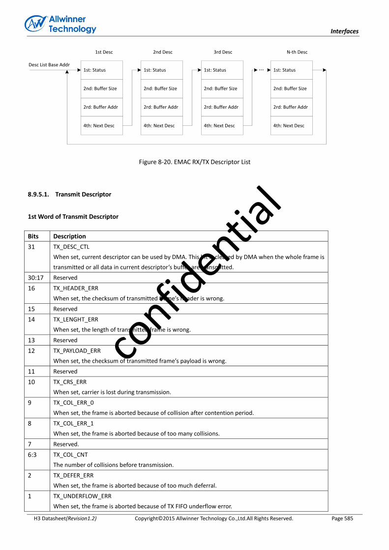
Interfaces
H3 Datasheet(Revision1.2) Copyright© 2015 Allwinner Technology Co.,Ltd.All Rights Reserved. Page 585
4th: Next Desc
1st: Status
2nd: Buffer Size
2rd: Buffer Addr
1st Desc 2nd Desc 3rd Desc N-th Desc
…Desc List Base Addr
4th: Next Desc
1st: Status
2nd: Buffer Size
2rd: Buffer Addr
4th: Next Desc
1st: Status
2nd: Buffer Size
2rd: Buffer Addr
4th: Next Desc
1st: Status
2nd: Buffer Size
2rd: Buffer Addr
Figure 8-20. EMAC RX/TX Descriptor List
8.9.5.1. Transmit Descriptor
1st Word of Transmit Descriptor
Bits Description
31 TX_DESC_CTL
When set, current descriptor can be used by DMA. This bit is cleared by DMA when the whole frame is
transmitted or all data in current descriptor’s buffer are transmitted.
30:17 Reserved
16 TX_HEADER_ERR
When set, the checksum of transmitted frame’s header is wrong.
15 Reserved
14 TX_LENGHT_ERR
When set, the length of transmitted frame is wrong.
13 Reserved
12 TX_PAYLOAD_ERR
When set, the checksum of transmitted frame’s payload is wrong.
11 Reserved
10 TX_CRS_ERR
When set, carrier is lost during transmission.
9 TX_COL_ERR_0
When set, the frame is aborted because of collision after contention period.
8 TX_COL_ERR_1
When set, the frame is aborted because of too many collisions.
7 Reserved.
6:3 TX_COL_CNT
The number of collisions before transmission.
2 TX_DEFER_ERR
When set, the frame is aborted because of too much deferral.
1 TX_UNDERFLOW_ERR
When set, the frame is aborted because of TX FIFO underflow error.
confid
ential
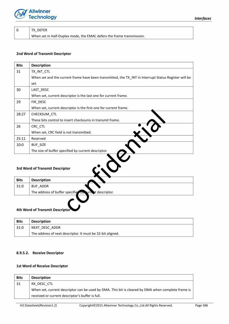
Interfaces
H3 Datasheet(Revision1.2) Copyright© 2015 Allwinner Technology Co.,Ltd.All Rights Reserved. Page 586
0 TX_DEFER
When set in Half-Duplex mode, the EMAC defers the frame transmission.
2nd Word of Transmit Descriptor
Bits Description
31 TX_INT_CTL
When set and the current frame have been transmitted, the TX_INT in Interrupt Status Register will be
set.
30 LAST_DESC
When set, current descriptor is the last one for current frame.
29 FIR_DESC
When set, current descriptor is the first one for current frame.
28:27 CHECKSUM_CTL
These bits control to insert checksums in transmit frame.
26 CRC_CTL
When set, CRC field is not transmitted.
25:11 Reserved
10:0 BUF_SIZE
The size of buffer specified by current descriptor.
3rd Word of Transmit Descriptor
Bits Description
31:0 BUF_ADDR
The address of buffer specified by current descriptor.
4th Word of Transmit Descriptor
Bits Description
31:0 NEXT_DESC_ADDR
The address of next descriptor. It must be 32-bit aligned.
8.9.5.2. Receive Descriptor
1st Word of Receive Descriptor
Bits Description
31 RX_DESC_CTL
When set, current descriptor can be used by DMA. This bit is cleared by DMA when complete frame is
received or current descriptor’s buffer is full.
confid
ential

Interfaces
H3 Datasheet(Revision1.2) Copyright© 2015 Allwinner Technology Co.,Ltd.All Rights Reserved. Page 587
30 RX_DAF_FAIL
When set, current frame don’t pass DA filter.
29:16 RX_FRM_LEN
When LAST_DESC is not set and no error bit is set, this field is the length of received data for current
frame.
When LAST_DESC is set, RX_OVERFLOW_ERR and RX_NO_ENOUGH_BUF_ERR are not set, this field is
the length of receive frame.
15 Reserved
14 RX_NO_ENOUGH_BUF_ERR
When set, current frame is clipped because of no enough buffer.
13 RX_SAF_FAIL
When set, current fame don’t pass SA filter.
12 Reserved.
11 RX_OVERFLOW_ERR
When set, a buffer overflow error occurred and current frame is wrong.
10 Reserved
9 FIR_DESC
When set, current descriptor is the first descriptor for current frame.
8 LAST_DESC
When set, current descriptor is the last descriptor for current frame.
7 RX_HEADER_ERR
When set, the checksum of frame’s header is wrong.
6 RX_COL_ERR
When set, there is a late collision during reception in half-duplex mode.
5 Reserved.
4 RX_LENGTH_ERR
When set, the length of current frame is wrong.
3 RX_PHY_ERR
When set, the receive error signal from PHY is asserted during reception.
2 Reserved.
1 RX_CRC_ERR
When set, the CRC filed of received frame is wrong.
0 RX_PAYLOAD_ERR
When set, the checksum or length of received frame’s payload is wrong.
2nd Word of Receive Descriptor
Bits Description
31 RX_INT_CTL
When set and a frame have been received, the RX_INT will not be set.
30:11 Reserved
10:0 BUF_SIZE
The size of buffer specified by current descriptor.
confid
ential
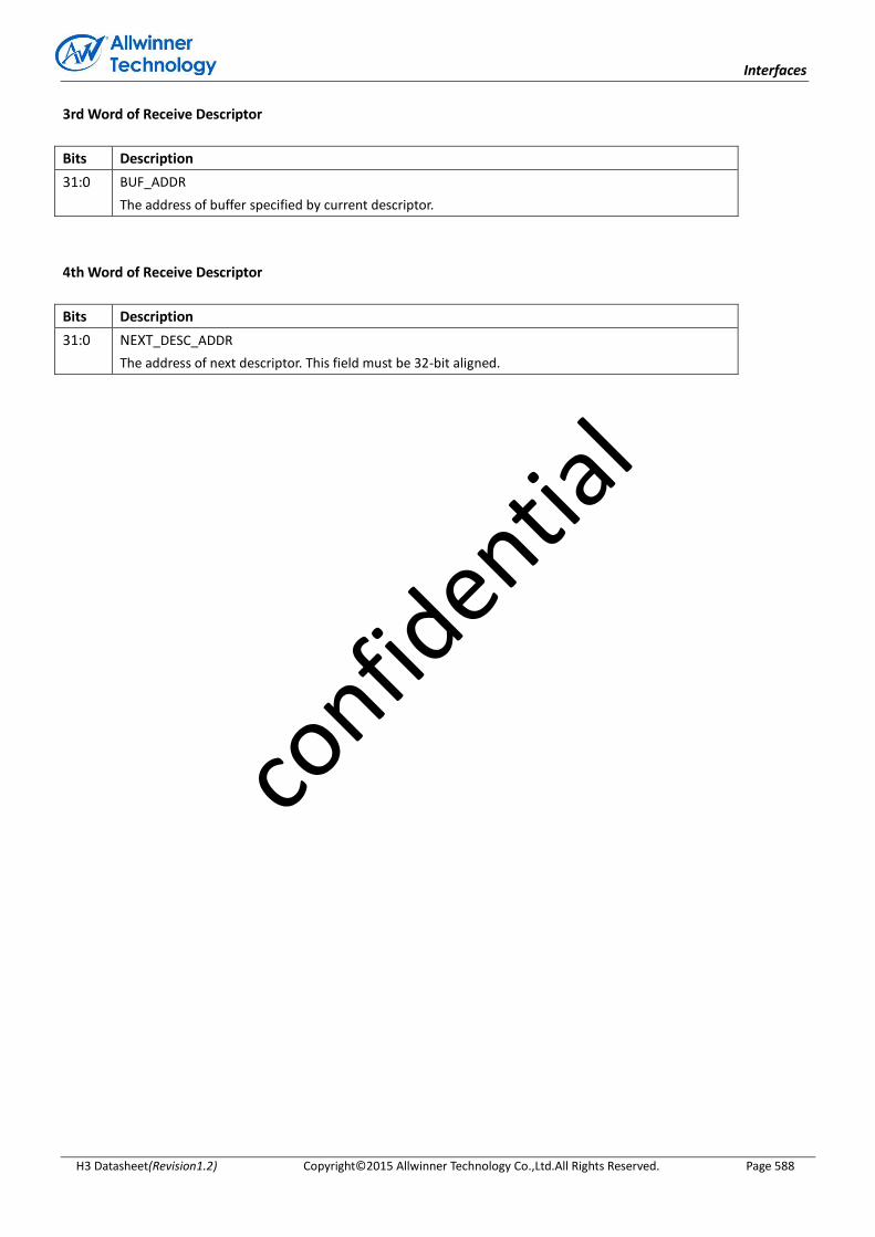
Interfaces
H3 Datasheet(Revision1.2) Copyright© 2015 Allwinner Technology Co.,Ltd.All Rights Reserved. Page 588
3rd Word of Receive Descriptor
Bits Description
31:0 BUF_ADDR
The address of buffer specified by current descriptor.
4th Word of Receive Descriptor
Bits Description
31:0 NEXT_DESC_ADDR
The address of next descriptor. This field must be 32-bit aligned.
confid
ential
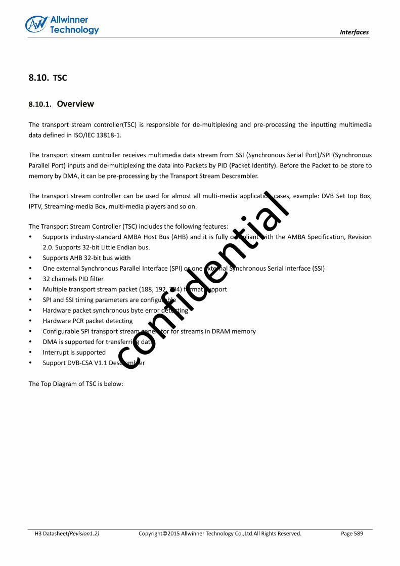
Interfaces
H3 Datasheet(Revision1.2) Copyright© 2015 Allwinner Technology Co.,Ltd.All Rights Reserved. Page 589
8.10. TSC
8.10.1. Overview
The transport stream controller(TSC) is responsible for de-multiplexing and pre-processing the inputting multimedia
data defined in ISO/IEC 13818-1.
The transport stream controller receives multimedia data stream from SSI (Synchronous Serial Port)/SPI (Synchronous
Parallel Port) inputs and de-multiplexing the data into Packets by PID (Packet Identify). Before the Packet to be store to
memory by DMA, it can be pre-processing by the Transport Stream Descrambler.
The transport stream controller can be used for almost all multi-media application cases, example: DVB Set top Box,
IPTV, Streaming-media Box, multi-media players and so on.
The Transport Stream Controller (TSC) includes the following features:
Supports industry-standard AMBA Host Bus (AHB) and it is fully compliant with the AMBA Specification, Revision
2.0. Supports 32-bit Little Endian bus.
Supports AHB 32-bit bus width
One external Synchronous Parallel Interface (SPI) or one external Synchronous Serial Interface (SSI)
32 channels PID filter
Multiple transport stream packet (188, 192, 204) format support
SPI and SSI timing parameters are configurable
Hardware packet synchronous byte error detecting
Hardware PCR packet detecting
Configurable SPI transport stream generator for streams in DRAM memory
DMA is supported for transferring data
Interrupt is supported
Support DVB-CSA V1.1 Descrambler
The Top Diagram of TSC is below:
confid
ential

Interfaces
H3 Datasheet(Revision1.2) Copyright© 2015 Allwinner Technology Co.,Ltd.All Rights Reserved. Page 590
Figure 8-21. TSC Block Diagram
Note:
TSC – TS Controller
TSF – TS Filter
TSD – TS Descrambler
TSG – TS Generator
8.10.2. Transport Stream Input Timing Diagram
Table 8-1. Input Signals Description
Name Description
Clock Clock of SPI/SSI data input
Psync Packet sync (or Start flag) for TS packet
Dvalid Data valid flag for TS data input
Error Error flag for TS data, but do not used by TSC
Data[7:0] TS data input.
Data[7:0] are used in SPI mode;
Only Data[0] is used in SSI mode.
confid
ential
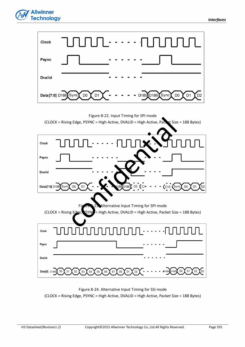
Interfaces
H3 Datasheet(Revision1.2) Copyright© 2015 Allwinner Technology Co.,Ltd.All Rights Reserved. Page 591
Figure 8-22. Input Timing for SPI mode
(CLOCK = Rising Edge, PSYNC = High Active, DVALID = High Active, Packet Size = 188 Bytes)
Figure 8-23. Alternative Input Timing for SPI mode
(CLOCK = Rising Edge, PSYNC = High Active, DVALID = High Active, Packet Size = 188 Bytes)
Figure 8-24. Alternative Input Timing for SSI mode
(CLOCK = Rising Edge, PSYNC = High Active, DVALID = High Active, Packet Size = 188 Bytes)
confid
ential

Interfaces
H3 Datasheet(Revision1.2) Copyright© 2015 Allwinner Technology Co.,Ltd.All Rights Reserved. Page 592
8.10.3. Transport Stream Controller Register List
Module Name Base Address
TSC 0x01C06000
TSG OFFSET 0x00000040
TSF0 OFFSET 0x00000080
TSF1 OFFSET 0x00000100
TSD OFFSET 0x00000180
Register Name Offset Description
TSC_CTLR TSC + 0x00 TSC Control Register
TSC_STAR TSC + 0x04 TSC Status Register
TSC_PCTLR TSC + 0x10 TSC Port Control Register
TSC_PPARR TSC + 0x14 TSC Port Parameter Register
TSC_TSFMUXR TSC + 0x20 TSC TSF Input Multiplex Control Register
TSC_OUTMUXR TSC + 0x28 TSC Port Output Multiplex Control Register
TSG_CTLR TSG + 0x00 TSG Control Register
TSG_PPR TSG + 0x04 TSG Packet Parameter Register
TSG_STAR TSG + 0x08 TSG Status Register
TSG_CCR TSG + 0x0c TSG Clock Control Register
TSG_BBAR TSG + 0x10 TSG Buffer Base Address Register
TSG_BSZR TSG + 0x14 TSG Buffer Size Register
TSG_BPR TSG + 0x18 TSG Buffer Pointer Register
TSF_CTLR TSF + 0x00 TSF Control Register
TSF_PPR TSF + 0x04 TSF Packet Parameter Register
TSF_STAR TSF + 0x08 TSF Status Register
TSF_DIER TSF + 0x10 TSF DMA Interrupt Enable Register
TSF_OIER TSF + 0x14 TSF Overlap Interrupt Enable Register
TSF_DISR TSF + 0x18 TSF DMA Interrupt Status Register
TSF_OISR TSF + 0x1c TSF Overlap Interrupt Status Register
TSF_PCRCR TSF + 0x20 TSF PCR Control Register
TSF_PCRDR TSF + 0x24 TSF PCR Data Register
TSF_CENR TSF + 0x30 TSF Channel Enable Register
TSF_CPER TSF + 0x34 TSF Channel PES Enable Register
TSF_CDER TSF + 0x38 TSF Channel Descramble Enable Register
TSF_CINDR TSF + 0x3c TSF Channel Index Register
TSF_CCTLR TSF + 0x40 TSF Channel Control Register
TSF_CSTAR TSF + 0x44 TSF Channel Status Register
TSF_CCWIR TSF + 0x48 TSF Channel CW Index Register
TSF_CPIDR TSF + 0x4c TSF Channel PID Register
TSF_CBBAR TSF + 0x50 TSF Channel Buffer Base Address Register
TSF_CBSZR TSF + 0x54 TSF Channel Buffer Size Register
confid
ential

Interfaces
H3 Datasheet(Revision1.2) Copyright© 2015 Allwinner Technology Co.,Ltd.All Rights Reserved. Page 593
TSF_CBWPR TSF + 0x58 TSF Channel Buffer Write Pointer Register
TSF_CBRPR TSF + 0x5c TSF Channel Buffer Read Pointer Register
TSD_CTLR TSD + 0x00 TSD Control Register
TSD_STAR TSD + 0x04 TSD Status Register
TSD_CWIR TSD + 0x1c TSD Control Word Index Register
TSD_CWR TSD + 0x20 TSD Control Word Register
8.10.4. Transport Stream Controller Register Description
8.10.4.1. TSC Control Register(Default Value: 0x00000000)
Offset: 0x00 Register Name: TSC_CTLR
Bit R/W Default/Hex Description
31:0 / / /
8.10.4.2. TSC Status Register(Default Value: 0x00000000)
Offset: 0x04 Register Name: TSC_STAR
Bit R/W Default/Hex Description
31:0 / / /
8.10.4.3. TSC Port Control Register(Default Value: 0x00000000)
Offset: 0x10 Register Name: TSC_PCTLR
Bit R/W Default/Hex Description
31:1 / / /
0 R/W 0
TSInPort0Ctrl
TS Input Port0 Control
0 – SPI
1 – SSI
8.10.4.4. TSC Port Parameter Register(Default Value: 0x00000000)
Offset: 0x14 Register Name: TSC_PPARR
Bit R/W Default/Hex Description
31:8 / / /
7:0 R/W 0x00 TSInPort0Par
confid
ential
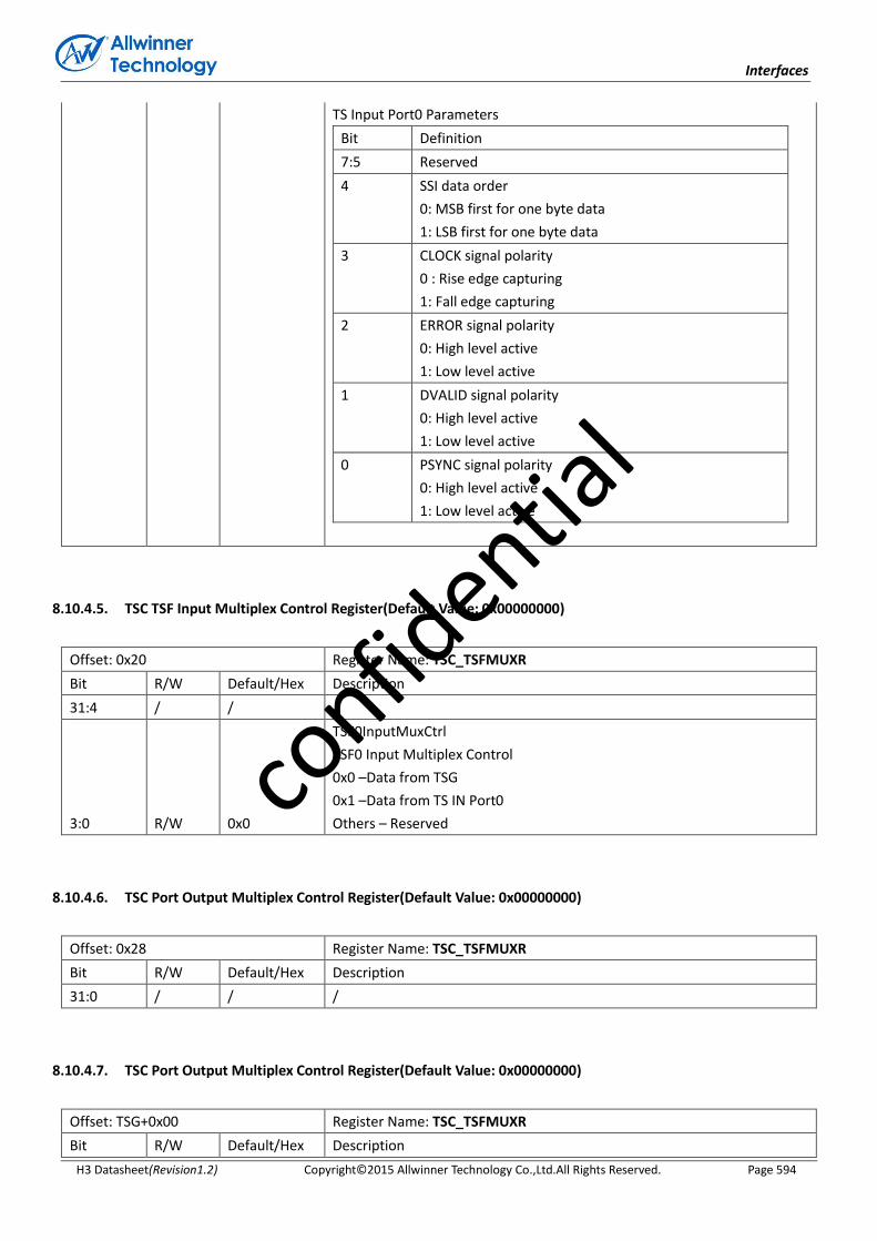
Interfaces
H3 Datasheet(Revision1.2) Copyright© 2015 Allwinner Technology Co.,Ltd.All Rights Reserved. Page 594
TS Input Port0 Parameters
Bit Definition
7:5 Reserved
4 SSI data order
0: MSB first for one byte data
1: LSB first for one byte data
3 CLOCK signal polarity
0 : Rise edge capturing
1: Fall edge capturing
2 ERROR signal polarity
0: High level active
1: Low level active
1 DVALID signal polarity
0: High level active
1: Low level active
0 PSYNC signal polarity
0: High level active
1: Low level active
8.10.4.5. TSC TSF Input Multiplex Control Register(Default Value: 0x00000000)
Offset: 0x20 Register Name: TSC_TSFMUXR
Bit R/W Default/Hex Description
31:4 / / /
3:0 R/W 0x0
TSF0InputMuxCtrl
TSF0 Input Multiplex Control
0x0 –Data from TSG
0x1 –Data from TS IN Port0
Others – Reserved
8.10.4.6. TSC Port Output Multiplex Control Register(Default Value: 0x00000000)
Offset: 0x28 Register Name: TSC_TSFMUXR
Bit R/W Default/Hex Description
31:0 / / /
8.10.4.7. TSC Port Output Multiplex Control Register(Default Value: 0x00000000)
Offset: TSG+0x00 Register Name: TSC_TSFMUXR
Bit R/W Default/Hex Description
confid
ential

Interfaces
H3 Datasheet(Revision1.2) Copyright© 2015 Allwinner Technology Co.,Ltd.All Rights Reserved. Page 595
31:26 / / /
25:24 R 0
TSGSts
Status for TS Generator
0: IDLE state
1: Running state
2: PAUSE state
Others: Reserved
23:10 / / /
9 R/W 0
TSGLBufMode
Loop Buffer Mode
When set to ‘1’, the TSG external buffer is in loop mode.
8 R/W 0
TSGSyncByteChkEn
Sync Byte Check Enable
Enable/ Disable check SYNC byte fro receiving new packet
0: Disable
1: Enable
If enable check SYNC byte and an error SYNC byte is receiver, TS Generator
would come into PAUSE state. If the correspond interrupt is enable, the
interrupt would happen.
7:3 / / /
2 R/W 0
TSGPauseBit
Pause Bit for TS Generator
Write ‘1’ to pause TS Generator. TS Generator would stop fetch new data
from DRAM. After finishing this operation, this bit will clear to zero by
hardware. In PAUSE state, write ‘1’ to resume this state.
1 R/W 0
TSGStopBit
Stop Bit for TS Generator
Write ‘1’ to stop TS Generator. TS Generator would stop fetch new data
from DRAM. The data already in its FIFO should be sent to TS filter. After
finishing this operation, this bit will clear to zero by hardware.
0 R/W 0
TSGStartBit
Start Bit for TS Generator
Write ‘1’ to start TS Generator. TS Generator would fetch data from DRAM
and generate SPI stream to TS filter. This bit will clear to zero by hardware
after TS Generator is running.
8.10.4.8. TSG Packet Parameter Register(Default Value: 0x00470000)
Offset: TSG+0x04 Register Name: TSG_PPR
Bit R/W Default/Hex Description
31:24 / / /
23:16 R/W 0x47
SyncByteVal
Sync Byte Value
This is the value of sync byte used in the TS Packet.
confid
ential

Interfaces
H3 Datasheet(Revision1.2) Copyright© 2015 Allwinner Technology Co.,Ltd.All Rights Reserved. Page 596
15:8 / / /
7 R/W 0
SyncBytePos
Sync Byte Position
0: the 1st byte position
1: the 5th byte position
Notes: This bit is only used for 192 bytes packet size.
6:2 / / /
1:0 R/W 0
PktSize
Packet Size
Byte Size for one TS packet
0: 188 bytes
Others: Reserved
8.10.4.9. TSG Interrupt Enable and Status Register(Default Value: 0x00000000)
Offset: TSG+0x08 Register Name: TSG_IESR
Bit R/W Default/Hex Description
31:20 / / /
19 R/W 0
TSGEndIE
TS Generator (TSG) End Interrupt Enable
0: Disable
1: Enable
If set this bit, the interrupt would assert to CPU when all data in external
DRAM are sent to TS PID filter.
18 R/W 0
TSGFFIE
TS Generator (TSG) Full Finish Interrupt Enable
0: Disable
1: Enable
17 R/W 0
TSGHFIE
TS Generator (TSG) Half Finish Interrupt Enable
0: Disable
1: Enable
16 R/W 0
TSGErrSyncByteIE
TS Generator (TSG) Error Sync Byte Interrupt Enable
0: Disable
1: Enable
15:4 / / /
3 R/W 0
TSGEndSts
TS Generator (TSG) End Status
Write ‘1’ to clear.
2 R/W 0
TSGFFSts
TS Generator (TSG) Full Finish Status
Write ‘1’ to clear.
1 R/W 0 TSGHFSts
confid
ential

Interfaces
H3 Datasheet(Revision1.2) Copyright© 2015 Allwinner Technology Co.,Ltd.All Rights Reserved. Page 597
TS Generator (TSG) Half Finish Status
Write ‘1’ to clear.
0 R/W 0
TSGErrSyncByteSts
TS Generator (TSG) Error Sync Byte Status
Write ‘1’ to clear.
8.10.4.10. TSG Clock Control Register(Default Value: 0x00000000)
Offset: TSG+0x0C Register Name: TSG_CCR
Bit R/W Default/Hex Description
31:16 R/W 0x0
TSGCDF_N
TSG Clock Divide Factor (N)
The Numerator part of TSG Clock Divisor Factor.
15:0 R/W 0x0
TSGCDF_D
TSG Clock Divide Factor (D)
The Denominator part of TSG Clock Divisor Factor.
Frequency of output clock:
Fo = (Fi*(N+1))/(8*(D+1)).
Fi is the input special clock of TSC, and D must not less than N.
8.10.4.11. TSG Buffer Base Address Register(Default Value: 0x00000000)
Offset: TSG+0x10 Register Name: TSG_BBAR
Bit R/W Default/Hex Description
31:28 / / /
27:0 RW 0x0
TSGBufBase
Buffer Base Address
This value is a start address of TSG buffer.
Note: This value should be 4-word (16Bytes) align, and the lowest 4-bit of
this value should be zero.
8.10.4.12. TSG Buffer Size Register(Default Value: 0x00000000)
Offset: TSG+0x14 Register Name: TSG_BSZR
Bit R/W Default/Hex Description
31:24 / / /
23:0 R/W 0
TSGBufSize
Data Buffer Size for TS Generator
It is in byte unit.
The size should be 4-word (16Bytes) align, and the lowest 4 bits should be
zero.
confid
ential

Interfaces
H3 Datasheet(Revision1.2) Copyright© 2015 Allwinner Technology Co.,Ltd.All Rights Reserved. Page 598
8.10.4.13. TSG Buffer Point Register(Default Value: 0x00000000)
Offset: TSG+0x18 Register Name: TSG_BPR
Bit R/W Default/Hex Description
31:24 / / /
23:0 R 0
TSGBufPtr
Data Buffer Pointer for TS Generator
Current TS generator data buffer read pointer (in byte unit)
8.10.4.14. TSF Control and Status Register(Default Value: 0x00000000)
Offset: TSF+0x00 Register Name: TSF_CSR
Bit R/W Default/Hex Description
31:3 / / /
2 R/W 0
TSF Enable
0: Disable TSF Input
1: Enable TSF Input
1 / / /
0
TSFGSR
TSF Global Soft Reset
A software writing ‘1’ will reset all status and state machine of TSF. And it’s
cleared by hardware after finish reset.
A software writing ‘0’ has no effect.
8.10.4.15. TSF Packet Parameter Register(Default Value: 0x00470000)
Offset: TSF+0x04 Register Name: TSF_PPR
Bit R/W Default/Hex Description
31:28 R/W 0
LostSyncThd
Lost Sync Packet Threshold
It is used for packet sync lost by checking the value of sync byte.
27:24 R/W 0
SyncThd
Sync Packet Threshold
It is used for packet sync by checking the value of sync byte.
23:16 R/W 0x47
SyncByteVal
Sync Byte Value
This is the value of sync byte used in the TS Packet.
15:10 / / /
9:8 R/W 0
SyncMthd
Packet Sync Method
0: By PSYNC signal
1: By sync byte
confid
ential
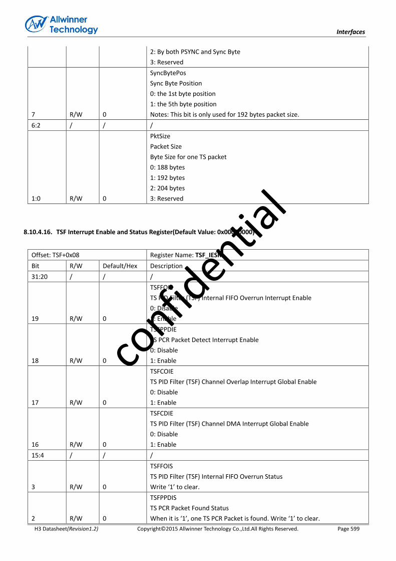
Interfaces
H3 Datasheet(Revision1.2) Copyright© 2015 Allwinner Technology Co.,Ltd.All Rights Reserved. Page 599
2: By both PSYNC and Sync Byte
3: Reserved
7 R/W 0
SyncBytePos
Sync Byte Position
0: the 1st byte position
1: the 5th byte position
Notes: This bit is only used for 192 bytes packet size.
6:2 / / /
1:0 R/W 0
PktSize
Packet Size
Byte Size for one TS packet
0: 188 bytes
1: 192 bytes
2: 204 bytes
3: Reserved
8.10.4.16. TSF Interrupt Enable and Status Register(Default Value: 0x00000000)
Offset: TSF+0x08 Register Name: TSF_IESR
Bit R/W Default/Hex Description
31:20 / / /
19 R/W 0
TSFFOIE
TS PID Filter (TSF) Internal FIFO Overrun Interrupt Enable
0: Disable
1: Enable
18 R/W 0
TSFPPDIE
TS PCR Packet Detect Interrupt Enable
0: Disable
1: Enable
17 R/W 0
TSFCOIE
TS PID Filter (TSF) Channel Overlap Interrupt Global Enable
0: Disable
1: Enable
16 R/W 0
TSFCDIE
TS PID Filter (TSF) Channel DMA Interrupt Global Enable
0: Disable
1: Enable
15:4 / / /
3 R/W 0
TSFFOIS
TS PID Filter (TSF) Internal FIFO Overrun Status
Write ‘1’ to clear.
2 R/W 0
TSFPPDIS
TS PCR Packet Found Status
When it is ‘1’, one TS PCR Packet is found. Write ‘1’ to clear.
confid
ential

Interfaces
H3 Datasheet(Revision1.2) Copyright© 2015 Allwinner Technology Co.,Ltd.All Rights Reserved. Page 600
1 R 0
TSFCOIS
TS PID Filter (TSF) Channel Overlap Status
It is global status for 16 channel. It would clear to zero after all channels
status bits are clear.
0 R 0
TSFCDIS
TS PID Filter (TSF) Channel DMA status
It is global status for 16 channel. It would clear to zero after all channels
status bits are clear.
8.10.4.17. TSF DMA Interrupt Enable Register(Default Value: 0x00000000)
Offset: TSF+0x10 Register Name: TSF_DIER
Bit R/W Default/Hex Description
31:0 R/W 0x0
DMAIE
DMA Interrupt Enable
DMA interrupt enable bits for channel 0~31.
8.10.4.18. TSF Overlap Interrupt Enable Register(Default Value: 0x00000000)
Offset: TSF+0x14 Register Name: TSF_OIER
Bit R/W Default/Hex Description
31:0 R/W 0x0
OLPIE
Overlap Interrupt Enable
Overlap interrupt enable bits for channel 0~31.
8.10.4.19. TSF DMA Interrupt Status Register(Default Value: 0x00000000)
Offset: TSF+0x18 Register Name: TSF_DISR
Bit R/W Default/Hex Description
31:0 R/W 0x0
DMAIS
DMA Interrupt Status
DMA interrupt Status bits for channel 0~31.
Set by hardware, and can be cleared by software writing ‘1’.
When both these bits and the corresponding DMA Interrupt Enable bits
set, the TSF interrupt will generate.
8.10.4.20. TSF Overlap Interrupt Status Register(Default Value: 0x00000000)
Offset: TSF+0x1C Register Name: TSF_OISR
confid
ential

Interfaces
H3 Datasheet(Revision1.2) Copyright© 2015 Allwinner Technology Co.,Ltd.All Rights Reserved. Page 601
Bit R/W Default/Hex Description
31:0 R/W 0x0
OLPIS
Overlap Interrupt Status
Overlap interrupt Status bits for channel 0~31.
Set by hardware, and can be cleared by software writing ‘1’.
When both these bits and the corresponding Overlap Interrupt Enable bits
set, the TSF interrupt will generate.
8.10.4.21. TSF PCR Control Register(Default Value: 0x00000000)
Offset: TSF+0x20 Register Name: TSF_PCRCR
Bit R/W Default/Hex Description
31:17 / / /
16 R/W 0
PCRDE
PCR Detecting Enable
0: Disable
1: Enable
15:13 / / /
12:8 R/W 0
PCRCIND
Channel Index m for Detecting PCR packet (m from 0 to 31)
7:1 / / /
0 R 0
PCRLSB
PCR Contest LSB 1 bit
PCR[0]
8.10.4.22. TSF PCR Data Register(Default Value: 0x00000000)
Offset: TSF+0x24 Register Name: TSF_PCRDR
Bit R/W Default/Hex Description
31:0 R 0
PCRMSB
PCR Data High 32 bits
PCR[33:1]
8.10.4.23. TSF Channel Enable Register(Default Value: 0x00000000)
Offset: TSF+0x30 Register Name: TSF_CENR
Bit R/W Default/Hex Description
31:0 R/W 0
FilterEn
Filter Enable for Channel 0~31
0: Disable
1: Enable
confid
ential
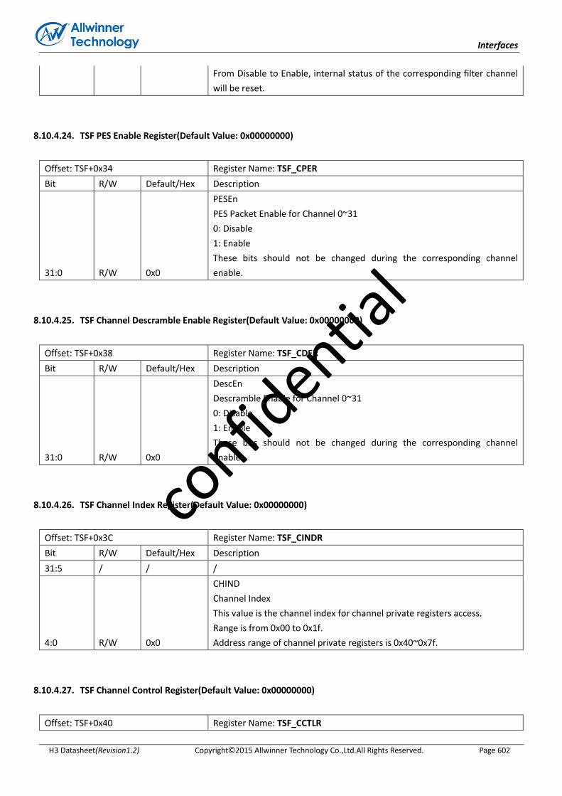
Interfaces
H3 Datasheet(Revision1.2) Copyright© 2015 Allwinner Technology Co.,Ltd.All Rights Reserved. Page 602
From Disable to Enable, internal status of the corresponding filter channel
will be reset.
8.10.4.24. TSF PES Enable Register(Default Value: 0x00000000)
Offset: TSF+0x34 Register Name: TSF_CPER
Bit R/W Default/Hex Description
31:0 R/W 0x0
PESEn
PES Packet Enable for Channel 0~31
0: Disable
1: Enable
These bits should not be changed during the corresponding channel
enable.
8.10.4.25. TSF Channel Descramble Enable Register(Default Value: 0x00000000)
Offset: TSF+0x38 Register Name: TSF_CDER
Bit R/W Default/Hex Description
31:0 R/W 0x0
DescEn
Descramble Enable for Channel 0~31
0: Disable
1: Enable
These bits should not be changed during the corresponding channel
enable.
8.10.4.26. TSF Channel Index Register(Default Value: 0x00000000)
Offset: TSF+0x3C Register Name: TSF_CINDR
Bit R/W Default/Hex Description
31:5 / / /
4:0 R/W 0x0
CHIND
Channel Index
This value is the channel index for channel private registers access.
Range is from 0x00 to 0x1f.
Address range of channel private registers is 0x40~0x7f.
8.10.4.27. TSF Channel Control Register(Default Value: 0x00000000)
Offset: TSF+0x40 Register Name: TSF_CCTLR
confid
ential
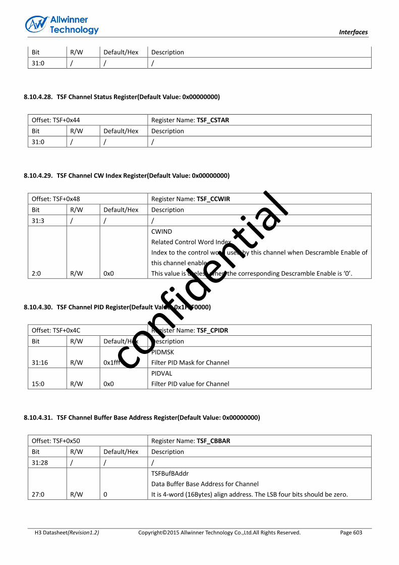
Interfaces
H3 Datasheet(Revision1.2) Copyright© 2015 Allwinner Technology Co.,Ltd.All Rights Reserved. Page 603
Bit R/W Default/Hex Description
31:0 / / /
8.10.4.28. TSF Channel Status Register(Default Value: 0x00000000)
Offset: TSF+0x44 Register Name: TSF_CSTAR
Bit R/W Default/Hex Description
31:0 / / /
8.10.4.29. TSF Channel CW Index Register(Default Value: 0x00000000)
Offset: TSF+0x48 Register Name: TSF_CCWIR
Bit R/W Default/Hex Description
31:3 / / /
2:0 R/W 0x0
CWIND
Related Control Word Index
Index to the control word used by this channel when Descramble Enable of
this channel enable.
This value is useless when the corresponding Descramble Enable is ‘0’.
8.10.4.30. TSF Channel PID Register(Default Value: 0x1FFF0000)
Offset: TSF+0x4C Register Name: TSF_CPIDR
Bit R/W Default/Hex Description
31:16 R/W 0x1fff
PIDMSK
Filter PID Mask for Channel
15:0 R/W 0x0
PIDVAL
Filter PID value for Channel
8.10.4.31. TSF Channel Buffer Base Address Register(Default Value: 0x00000000)
Offset: TSF+0x50 Register Name: TSF_CBBAR
Bit R/W Default/Hex Description
31:28 / / /
27:0 R/W 0
TSFBufBAddr
Data Buffer Base Address for Channel
It is 4-word (16Bytes) align address. The LSB four bits should be zero.
confid
ential

Interfaces
H3 Datasheet(Revision1.2) Copyright© 2015 Allwinner Technology Co.,Ltd.All Rights Reserved. Page 604
8.10.4.32. TSF Channel Buffer Size Register(Default Value: 0x00000000)
Offset: TSF+0x54 Register Name: TSF_CBSZR
Bit R/W Default/Hex Description
31:26 / / /
25:24 R/W 0
CHDMAIntThd
DMA Interrupt Threshold for Channel
The unit is TS packet size. When received packet (has also stored in DRAM)
size is beyond (>=) threshold value, the corresponding channel interrupt is
generated to CPU. TSC should count the new received packet again, when
exceed the specified threshold value, one new interrupt is generated again.
0: 1/2 data buffer packet size
1: 1/4 data buffer packet size
2: 1/8 data buffer packet size
3: 1/16 data buffer packet size
23:21 / / /
20:0 R/W 0
CHBufPktSz
Data Buffer Packet Size for Channel
The exact buffer size of buffer is N+1 bytes.
The maximum buffer size is 2MB.
This size should be 4-word (16Bytes) aligned. The LSB four bits should be
zero.
8.10.4.33. TSF Channel Write Pointer Register(Default Value: 0x00000000)
Offset: TSF+0x58 Register Name: TSF_CBWPR
Bit R/W Default/Hex Description
31:21 / / /
20:0 R/W 0
BufWrPtr
Data Buffer Write Pointer (in Bytes)
This value is changed by hardware, when data is filled into buffer, this
pointer is increased.
And this pointer can be set by software, but it should not be changed by
software during the corresponding channel is enable.
8.10.4.34. TSF Channel Read Pointer Register(Default Value: 0x00000000)
Offset: TSF+0x5C Register Name: TSF_CBRPR
Bit R/W Default/Hex Description
31:21 / / /
20:0 R/W 0
BufRdPtr
Data Buffer Read Pointer (in Bytes)
confid
ential

Interfaces
H3 Datasheet(Revision1.2) Copyright© 2015 Allwinner Technology Co.,Ltd.All Rights Reserved. Page 605
This pointer should be changed by software after the data of buffer is read.
8.10.4.35. TSD Control Register(Default Value: 0x00000000)
Offset: TSD+0x00 Register Name: TSD_CTLR
Bit R/W Default/Hex Description
31:2 / / /
1:0 R/W 0x0
DescArith
Descramble Arithmetic
00: DVB CSA V1.1
Others: Reserved
8.10.4.36. TSD Status Register(Default Value: 0x00000000)
Offset: TSD+0x04 Register Name: TSD_STAR
Bit R/W Default/Hex Description
31:0 / / /
8.10.4.37. TSD Control Word Index Register(Default Value: 0x00000000)
Offset: TSD+0x1C Register Name: TSD_CWIR
Bit R/W Default/Hex Description
31:3 / / /
6:4 R/W 0x0
CWI
Control Word Index
This value is the Control index for Control word access.
Range is from 0x00 to 0x7.
3:2 / / /
1:0 R/W 0x0
CWII
Control Word Internal Index
0 – Odd Control Word Low 32-bit, OCW[31:0];
1 – Odd Control Word High 32-bit, OCW[63:32];
2 – Even Control Word Low 32-bit, ECW[31:0];
3 – Even Control Word High 32-bit, ECW[63:0];
8.10.4.38. TSD Control Word Register(Default Value: 0x00000000)
Offset: TSD+0x20 Register Name: TSD_CWR
Bit R/W Default/Hex Description
confid
ential

Interfaces
H3 Datasheet(Revision1.2) Copyright© 2015 Allwinner Technology Co.,Ltd.All Rights Reserved. Page 606
31:0 R/W 0x0
CWD
Content of Control Word corresponding to the TSD_CWIR value
confid
ential

Electrical Characteristics
H3 Datasheet(Revision1.2) Copyright© 2015 Allwinner Technology Co.,Ltd.All Rights Reserved. Page 607
Chapter 9 Electrical Characteristics
9.1. Absolute Maximum Ratings
Absolute Maximum Ratings are those values beyond which damage to the device may occur. Table 9-1 specifies the
absolute maximum ratings over the operating junction temperature range of commercial and extended temperature
devices. Functional operation of the device at these or any other conditions beyond those indicated in the operational
sections of this standard may damage to the device.
Table 9-1. Absolute Maximum Ratings
Symbol Parameter MIN Max Unit
II/O In/Out current for input and output -40 40 mA
AVCC Power Supply for Analog part -0.3 3.4 V
EPHY_VCC Power Supply for EPHY -0.3 3.8 V
EPHY_VDD Power Supply for EPHY -0.3 1.4 V
HVCC Power Supply for HDMI -0.3 3.6 V
V33_TV Power Supply for TV -0.3 3.6 V
VCC_IO Power Supply for Port A -0.3 3.6 V
VCC_PD Power Supply for Port D -0.3 3.6 V
VCC_PG Power Supply for Port G -0.3 3.6 V
VCC_PLL Power Supply for system PLL -0.3 3.6 V
VCC_RTC Power Supply for RTC -0.3 3.6 V
VCC_USB Power Supply for USB -0.3 3.6 V
VCC-DRAM Power Supply for DRAM -0.3 1.98 V
VDD_CPUS Power Supply for CPUS -0.3 1.4 V
VDD_CPUX Power Supply for CPU -0.3 1.5 V
VDD_EFUSE Power Supply for EFUSE -0.3 3.6 V
VDD_SYS Power Supply for System -0.3 1.4 V
TSTG Storage Temperature -40 125 °C
confid
ential
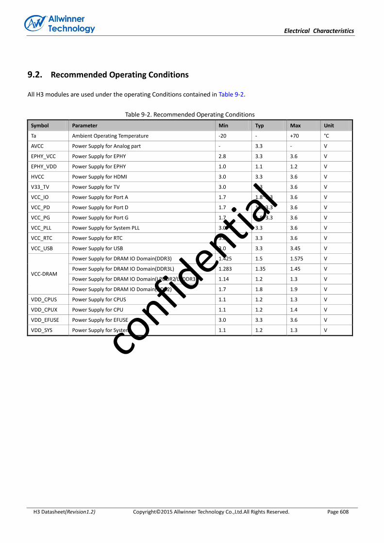
Electrical Characteristics
H3 Datasheet(Revision1.2) Copyright© 2015 Allwinner Technology Co.,Ltd.All Rights Reserved. Page 608
9.2. Recommended Operating Conditions
All H3 modules are used under the operating Conditions contained in Table 9-2.
Table 9-2. Recommended Operating Conditions
Symbol Parameter Min Typ Max Unit
Ta Ambient Operating Temperature -20 - +70 °C
AVCC Power Supply for Analog part - 3.3 - V
EPHY_VCC Power Supply for EPHY 2.8 3.3 3.6 V
EPHY_VDD Power Supply for EPHY 1.0 1.1 1.2 V
HVCC Power Supply for HDMI 3.0 3.3 3.6 V
V33_TV Power Supply for TV 3.0 3.3 3.6 V
VCC_IO Power Supply for Port A 1.7 1.8~3.3 3.6 V
VCC_PD Power Supply for Port D 1.7 1.8~3.3 3.6 V
VCC_PG Power Supply for Port G 1.7 1.8~3.3 3.6 V
VCC_PLL Power Supply for System PLL 3.0 3.3 3.6 V
VCC_RTC Power Supply for RTC 3.0 3.3 3.6 V
VCC_USB Power Supply for USB 3.0 3.3 3.45 V
VCC-DRAM
Power Supply for DRAM IO Domain(DDR3) 1.425 1.5 1.575 V
Power Supply for DRAM IO Domain(DDR3L) 1.283 1.35 1.45 V
Power Supply for DRAM IO Domain(LPDDR2/LPDDR3) 1.14 1.2 1.3 V
Power Supply for DRAM IO Domain(DDR2) 1.7 1.8 1.9 V
VDD_CPUS Power Supply for CPUS 1.1 1.2 1.3 V
VDD_CPUX Power Supply for CPU 1.1 1.2 1.4 V
VDD_EFUSE Power Supply for EFUSE 3.0 3.3 3.6 V
VDD_SYS Power Supply for System 1.1 1.2 1.3 V
confid
ential

Electrical Characteristics
H3 Datasheet(Revision1.2) Copyright© 2015 Allwinner Technology Co.,Ltd.All Rights Reserved. Page 609
9.3. DC Electrical Characteristics
Table 9-2 summarizes the DC electrical characteristics of H3.
Table 9-3. DC Electrical Characteristics
Symbol Parameter Min Typ Max Unit
VIH High-Level Input Voltage 0.7*VCC_IO - VCC_IO+0.3 V
VIL Low-Level Input Voltage -0.3 - 0.3*VCC_IO V
RPU Input pull-up resistance 50 100 150 KΩ
RPD Input pull-down resistance 50 100 150 KΩ
IIH High-Level Input Current - - 10 uA
IIL Low-Level Input Current - - 10 uA
VOH High-Level Output Voltage VCC_IO-0.2 - VCC_IO V
VOL Low-Level Output Voltage 0 - 0.2 V
IOZ Tri-State Output Leakage
Current -10 - 10 uA
CIN Input Capacitance - - 5 pF
COUT Output Capacitance - - 5 pF
confid
ential
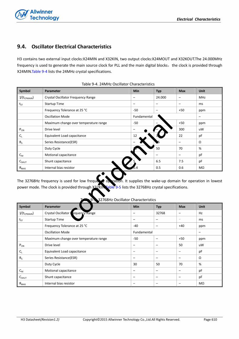
Electrical Characteristics
H3 Datasheet(Revision1.2) Copyright© 2015 Allwinner Technology Co.,Ltd.All Rights Reserved. Page 610
9.4. Oscillator Electrical Characteristics
H3 contains two external input clocks:X24MIN and X32KIN, two output clocks:X24MOUT and X32KOUT.The 24.000MHz
frequency is used to generate the main source clock for PLL and the main digital blocks,the clock is provided through
X24MIN.Table 9-4 lists the 24MHz crystal specifications.
Table 9-4. 24MHz Oscillator Characteristics
Symbol Parameter Min Typ Max Unit
1/(tCPMAIN) Crystal Oscillator Frequency Range – 24.000 – MHz
tST Startup Time – – – ms
Frequency Tolerance at 25 °C -50 – +50 ppm
Oscillation Mode Fundamental –
Maximum change over temperature range -50 – +50 ppm
PON Drive level – – 300 uW
CL Equivalent Load capacitance 12 18 22 pF
RS Series Resistance(ESR) – 25 – Ω
Duty Cycle 30 50 70 %
CM Motional capacitance – – – pF
CSHUT Shunt capacitance 5 6.5 7.5 pF
RBIAS Internal bias resistor 0.4 0.5 0.6 MΩ
The 32768Hz frequency is used for low frequency operation. It supplies the wake-up domain for operation in lowest
power mode. The clock is provided through X32KIN.Table 9-5 lists the 32768Hz crystal specifications.
Table 9-5. 32768Hz Oscillator Characteristics
Symbol Parameter Min Typ Max Unit
1/(tCPMAIN) Crystal Oscillator Frequency Range – 32768 – Hz
tST Startup Time – – - ms
Frequency Tolerance at 25 °C -40 – +40 ppm
Oscillation Mode Fundamental –
Maximum change over temperature range -50 – +50 ppm
PON Drive level – – 50 uW
CL Equivalent Load capacitance – – – pF
RS Series Resistance(ESR) – – – Ω
Duty Cycle 30 50 70 %
CM Motional capacitance – – – pF
CSHUT Shunt capacitance – – – pF
RBIAS Internal bias resistor – – – MΩ
confid
ential
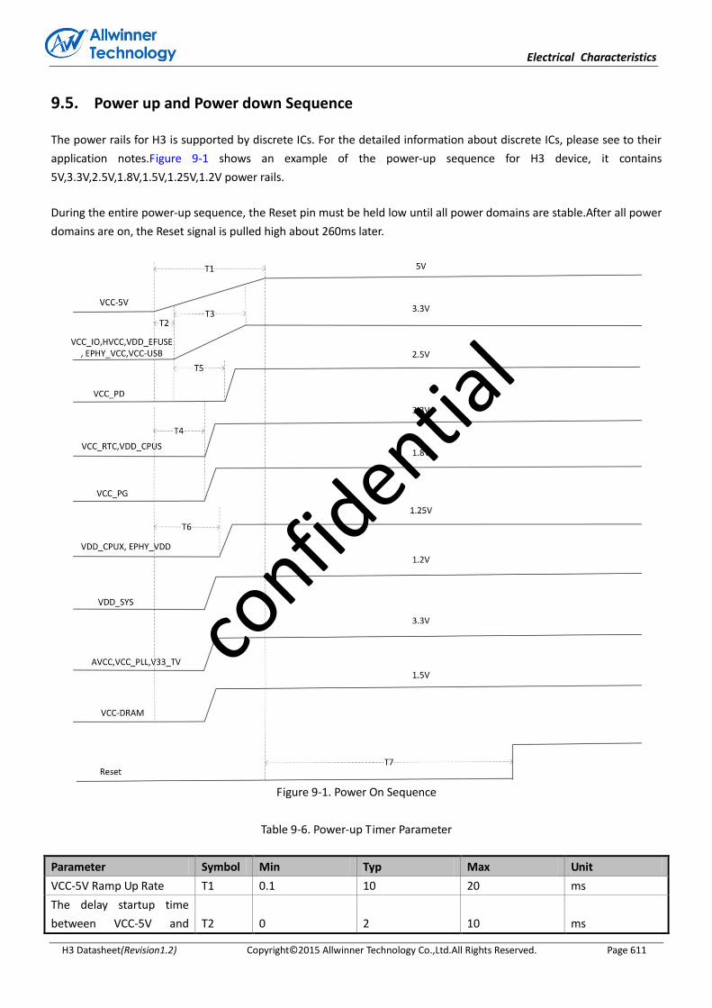
Electrical Characteristics
H3 Datasheet(Revision1.2) Copyright© 2015 Allwinner Technology Co.,Ltd.All Rights Reserved. Page 611
9.5. Power up and Power down Sequence
The power rails for H3 is supported by discrete ICs. For the detailed information about discrete ICs, please see to their
application notes.Figure 9-1 shows an example of the power-up sequence for H3 device, it contains
5V,3.3V,2.5V,1.8V,1.5V,1.25V,1.2V power rails.
During the entire power-up sequence, the Reset pin must be held low until all power domains are stable.After all power
domains are on, the Reset signal is pulled high about 260ms later.
Figure 9-1. Power On Sequence
Table 9-6. Power-up Timer Parameter
Parameter Symbol Min Typ Max Unit
VCC-5V Ramp Up Rate T1 0.1 10 20 ms
The delay startup time
between VCC-5V and T2 0 2 10 ms
confid
ential
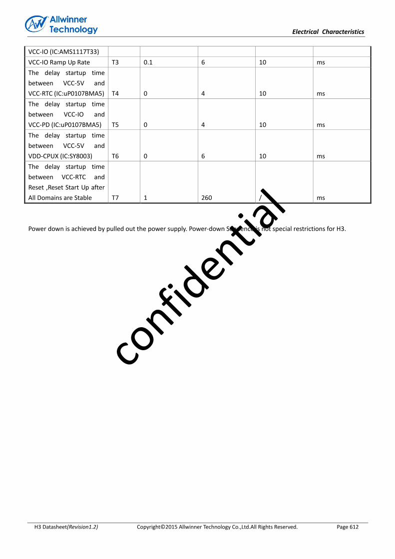
Electrical Characteristics
H3 Datasheet(Revision1.2) Copyright© 2015 Allwinner Technology Co.,Ltd.All Rights Reserved. Page 612
VCC-IO (IC:AMS1117T33)
VCC-IO Ramp Up Rate T3 0.1 6 10 ms
The delay startup time
between VCC-5V and
VCC-RTC (IC:uP0107BMA5) T4 0 4 10 ms
The delay startup time
between VCC-IO and
VCC-PD (IC:uP0107BMA5) T5 0 4 10 ms
The delay startup time
between VCC-5V and
VDD-CPUX (IC:SY8003) T6 0 6 10 ms
The delay startup time
between VCC-RTC and
Reset ,Reset Start Up after
All Domains are Stable T7 1 260 / ms
Power down is achieved by pulled out the power supply. Power-down Sequence is not special restrictions for H3.
confid
ential

Appendix
H3 Datasheet(Revision 1.2) Copyright© 2015 Allwinner Technology Co.,Ltd.All Rights Reserved. Page 613
Appendix
Pin Map
The following figure shows the pin maps of the 347-pin FBGA package of H3 processor.
1 2 3 4 5 6 7 8 9 10 11 12 13 14 15 16 17 18 19 20 21
A
JTAG-
SEL0
EPHY_
LINK_LE
D
EPHY_
TXN
EPHY_
RXN
USB_
DP0
USB_
DP2
USB_
DM2
PE1 PE11 PA20 PA21 PC7 PC5 PF1 PD4 GND A
B PG13
JTAG-
SEL1
EPHY_
TXP
EPHY_
RXP
USB_
DM0
USB_
DP1
USB_
DM1
USB_
DP3
USB_
DM3
PE0 PE2 PE12 PA18 PA19 PC3 PC2 PC12 PC8 PC13 PD2 PD6 B
C PG5 PG4 PG8 PE15 PE14 PE13 PE7 PE4 PE3 PE8 PE9 PA12 PA17 PC0 PC1 PC9 PC11 PC15 PF5 PD0 C
D PG12 PG11 PG7 PA1 PA2 PA7 PE6 PA0 PA9 PA16 PC10 PF0 PF2 D
E HTXCN PG9 PE10 PE5 PA10 PA3 PA6 PA13 PC6 PD7 PD12 PD8 PF4 E
F HTX0N HTXCP PG3 PA4
EPHY_
RTX
EPHY_
SPD_LE
D
EPHY_
VDD
TVOUT PA11 PA8 PA15 PC4 PC14 PF3 PD5 PD11 PD9 F
G HTX0P HTX1N PG6 HCEC
EPHY_
VCC GND V33_TV
VDD_
EFUSE
VCC_
USB PA14 VCC_IO VCC_IO VCC_IO PF6 SDQM1 G
H HTX1P HSCL PG2 PA5 VCC_PG GND_TV
VDD_
SYS
VDD_EF
USEBP GND VCC_IO VCC_IO GND PC16 PD1 PD3 PD10 SDQ9 SDQ10 H
J HTX2P HTX2N PG0 HVCC
VDD_
CPUS
VDD_
CPUS GND
VDD_
SYS
VDD_
SYS
VDD_
SYS GND VCC_IO VCC_PD GND SDQ8 SDQS1B SDQ11 J
K
X24MO
UT X24MIN HSDA NC
VCC_
RTC GND GND GND
VDD_
SYS
VDD_
SYS
VDD_
SYS GND GND GND GND PD13 PD15 SDQS1 K
L PG1 PLLTEST GND GND
VDD_
SYS
VDD_
SYS
VDD_
SYS
VDD_
SYS
VDD_
SYS GND
VCC-
DRAM PD14 PD16 PD17 SDQ12 SDQ13 L
M PL1 HHPD PG10 RTC_VIO HGND PL9 GND GND GND GND GND GND GND GND GND
VCC-
DRAM SDQ15 SDQM0 SDQ14 M
N PL0 PL4 VCC_PLL GND
VDD_
CPUX GND GND GND GND GND GND GND
VCC-
DRAM SA14 SA11 SDQ0 N
P PL2
X32KFO
UT
VDD_
CPUX
VDD_
CPUX
VDD_
CPUX
VDD_
CPUX GND GND GND GND GND GND
VCC-
DRAM
VCC-
DRAM SA10 SDQ2 SDQ1 P
R PL3 PL5
VDD_
CPUX
VDD_
CPUX
VDD_
CPUX GND GND GND GND GND GND
VCC-
DRAM SA15 SA12 SDQ4 SDQS0 SDQS0B R
T PL8 PL7 PL6 TEST
VDD_
CPUX
VDD_
CPUX
VDD_
CPUX
GND-
CPUFB
VDD_
CPUFB GND
VCC-
DRAM
VCC-
DRAM
VCC-
DRAM
VCC-
DRAM SVREF SA0 SBA1 SDQ5 T
U PL11 AGND
X32KOU
T
VDD_
CPUX
VDD_
CPUX
VCC-
DRAM SCAS SRST SA1 SDQ6 SDQ7 SDQ3 U
V LINEINL PL10 AVCC VRP X32KIN RESET SZQ SODT1 SA13 SRAS SA7 SBA2 SA2 SA3 SA4 V
W LINEINR MICIN1P MBIAS VRA2 UBOOT SDQ28 SODT0 SDQ24 SWE SDQ19 SBA0 SA8 SCS0 SCS1 W
Y
MICIN1
N MICIN2P
LINEOU
TR VRA1 SDQ31 SDQ30 SDQS3B SDQ27 SDQ26 SDQ23 SDQ22 SDQ20 SDQS2B SDQ18 SDQ16 SA9 SA5 SA6 SCKE1 Y
A
A GND
MICIN2
N
LINEOU
TL KEYADC NMI SDQ29 SDQS3 SDQ25 SDQM3 SDQ21 SDQS2 SDQ17 SDQM2 SCK SCKB SCKE0 AA
1 2 3 4 5 6 7 8 9 10 11 12 13 14 15 16 17 18 19 20 21
confid
ential
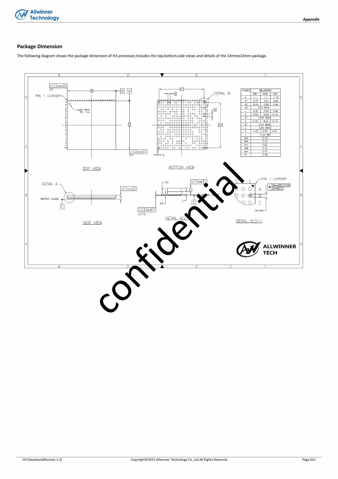
Appendix
H3 Datasheet(Revision 1.2) Copyright© 2015 Allwinner Technology Co.,Ltd.All Rights Reserved. Page 614
Package Dimension
The following diagram shows the package dimension of H3 processor,includes the top,bottom,side views and details of the 14mmx14mm package.
confid
ential


