62
Altera High-Definition Multimedia Interface IP Core User Guide Subscribe Send Feedback UG-HDMI 2015.05.04 101 Innovation Drive San Jose, CA 95134 www.altera.com
Altera High-Definition MultimediaInterface IP Core User Guide
Subscribe
Send Feedback
UG-HDMI2015.05.04
101 Innovation DriveSan Jose, CA 95134www.altera.com

Contents
HDMI Quick Reference.......................................................................................1-1
HDMI Overview.................................................................................................. 2-1Resource Utilization.................................................................................................................................... 2-4
HDMI Getting Started.........................................................................................3-1Installing and Licensing IP Cores.............................................................................................................. 3-1OpenCore Plus IP Evaluation.................................................................................................................... 3-2Specifying IP Core Parameters and Options............................................................................................3-2
HDMI Source.......................................................................................................4-1Source Functional Description.................................................................................................................. 4-1
Source TMDS/TERC4 Encoder..................................................................................................... 4-2Source Video Resampler................................................................................................................. 4-2Source Window of Opportunity Generator................................................................................. 4-3Source Auxiliary Packet Encoder...................................................................................................4-4Source Auxiliary Packet Generators..............................................................................................4-5Source Auxiliary Data Path Multiplexers..................................................................................... 4-5Source Auxiliary Control Port....................................................................................................... 4-5Source Audio Encoder.....................................................................................................................4-9
Source Parameters..................................................................................................................................... 4-10Source Interfaces........................................................................................................................................ 4-11Source Clock Tree......................................................................................................................................4-15
HDMI Sink...........................................................................................................5-1Sink Functional Description.......................................................................................................................5-1
Sink Channel Word Alignment and Deskew...............................................................................5-2Sink TMDS/TERC4 Decoder......................................................................................................... 5-3Sink Video Resampler..................................................................................................................... 5-4Sink Auxiliary Decoder................................................................................................................... 5-4Sink Auxiliary Packet Capture....................................................................................................... 5-5Sink Auxiliary Data Port................................................................................................................. 5-8Sink Audio Decoding.................................................................................................................... 5-11
Sink Parameters..........................................................................................................................................5-11Sink Interfaces............................................................................................................................................ 5-12
Avalon-MM SCDC Management Interface............................................................................... 5-17Sink Clock Tree.......................................................................................................................................... 5-17
HDMI Hardware Demonstration....................................................................... 6-1
TOC-2
Altera Corporation
HDMI Hardware Demonstration Requirements.................................................................................... 6-2Transceiver and Clocking Configuration................................................................................................. 6-6Software Process Flow...............................................................................................................................6-10Demonstration Walkthrough...................................................................................................................6-12
Set Up the Hardware..................................................................................................................... 6-12Copy the Design Files....................................................................................................................6-12Build the Design.............................................................................................................................6-12View the Results............................................................................................................................. 6-13
HDMI Simulation Example................................................................................ 7-1Simulation Walkthrough............................................................................................................................ 7-2
Additional Information for High-Definition Multimedia Interface UserGuide............................................................................................................... A-1
Document Revision History for HDMI User Guide..............................................................................A-1
TOC-3
Altera Corporation

HDMI Quick Reference 12015.05.04
UG-HDMI Subscribe Send Feedback
The Altera High-Definition Multimedia Interface (HDMI) IP core provides support for next-generationvideo display interface technology.
Release Information
Version 15.0Release May 2015Ordering Code IP-HDMIProduct ID 0121Vendor ID 6AF7
IP Core Information
Core Features • Conforms to the High-Definition MultimediaInterface (HDMI) specification version 2.0
• Supports transmitter and receiver on a singledevice transceiver quad
• Supports pixel frequency up to 594 MHz• Supports RGB and YCbCr color modes• Accepts standard H-SYNC, V-SYNC, data enable,
RGB video format, and YCbCr video format• Supports 2-channel audio• Supports 1, 2, or 4 symbols per clock
Typical Application • Interfaces within a PC and monitor• External display connections, including interfaces
between a PC and monitor or projector, betweena PC and TV, or between a device such as a DVDplayer and TV display
Device Family Supports Arria 10 (preliminary), Arria V, and StratixV FPGA devices
Design Tools • Quartus II software for IP design instantiationand compilation
• TimeQuest Timing Analyzer in the Quartus IIsoftware for timing analysis
• ModelSim-Altera/SE software for designsimulation
© 2015 Altera Corporation. All rights reserved. ALTERA, ARRIA, CYCLONE, ENPIRION, MAX, MEGACORE, NIOS, QUARTUS and STRATIX words and logos aretrademarks of Altera Corporation and registered in the U.S. Patent and Trademark Office and in other countries. All other words and logos identified astrademarks or service marks are the property of their respective holders as described at www.altera.com/common/legal.html. Altera warrants performanceof its semiconductor products to current specifications in accordance with Altera's standard warranty, but reserves the right to make changes to anyproducts and services at any time without notice. Altera assumes no responsibility or liability arising out of the application or use of any information,product, or service described herein except as expressly agreed to in writing by Altera. Altera customers are advised to obtain the latest version of devicespecifications before relying on any published information and before placing orders for products or services.
ISO9001:2008Registered
www.altera.com101 Innovation Drive, San Jose, CA 95134

HDMI Overview 22015.05.04
UG-HDMI Subscribe Send Feedback
The Altera High-Definition Multimedia Interface (HDMI) IP core provides support for next generationvideo display interface technology.
The HDMI standard specifies a digital communications interface for use in both internal and externalconnections:
• Internal connections—interface within a PC and monitor• External display connections—interface between a PC and monitor or projector, between a PC and
TV, or between a device such a DVD player and TV display.
The HDMI system architecture consists of sinks and sources. A device may have one or more HDMIinputs and outputs.
The HDMI cable and connectors carry four differential pairs that make up the Transition MinimizedDifferential Signaling (TMDS) data and clock channels. You can use these channels to carry video, audio,and auxiliary data.
The HDMI also carries a Video Electronics Standards Association (VESA) Display Data Channel (DDC)and Status and Control Data Channel (SCDC). The DDC configures and exchanges status between asingle source and a single sink. The source uses the DDC to read the sink's Enhanced Extended DisplayIdentification Data (E-EDID) to discover the sink's configuration and capabilities. The SCDC supportsthe sink's read requests.
The optional Consumer Electronics Control (CEC) protocol provides high-level control functionsbetween various audio visual products in your environment.
The optional HDMI Ethernet and Audio Return Channel (HEAC) provides Ethernet compatible datanetworking between connected devices and an audio return channel in the opposite direction of TMDS.The HEAC also uses Hot-Plug Detect (HPD) line for signal transmission.
© 2015 Altera Corporation. All rights reserved. ALTERA, ARRIA, CYCLONE, ENPIRION, MAX, MEGACORE, NIOS, QUARTUS and STRATIX words and logos aretrademarks of Altera Corporation and registered in the U.S. Patent and Trademark Office and in other countries. All other words and logos identified astrademarks or service marks are the property of their respective holders as described at www.altera.com/common/legal.html. Altera warrants performanceof its semiconductor products to current specifications in accordance with Altera's standard warranty, but reserves the right to make changes to anyproducts and services at any time without notice. Altera assumes no responsibility or liability arising out of the application or use of any information,product, or service described herein except as expressly agreed to in writing by Altera. Altera customers are advised to obtain the latest version of devicespecifications before relying on any published information and before placing orders for products or services.
ISO9001:2008Registered
www.altera.com101 Innovation Drive, San Jose, CA 95134

Figure 2-1: Altera HDMI Block Diagram
The figure below illustrates the blocks in the Altera HDMI IP core.
HDMITransmitter
HDMIReceiver
TDMS Channel 0
HDMI IP Core
TDMS Channel 1
TDMS Channel 2
TDMS Clock Channel
Video
Audio
Control/Status
Video
Audio
Control/Status
Detect
CEC
HEAC
EDID ROM
CEC
HEAC
CEC Line
Utility Line
HPD Line
Display Data Channel (DDC)
Status and Control Data Channel (SCDC)
High/Low
Based on TMDS encoding, the HDMI protocol allows the transmission of both audio and video databetween source and sink devices.
An HDMI interface consists of three color channels accompanied by a single clock channel. You can useeach color line to transfer both individual RGB colors and auxiliary data.
The receiver uses the TMDS clock as a frequency reference for data recovery on the three TMDS datachannels. This clock typically runs at the video pixel rate.
TMDS encoding is based on an 8-bit to 10-bit algorithm. This protocol attempts to minimize data channeltransmission and yet maintain sufficient bandwidth so that a sink device can lock reliably to the datastream.
2-2 HDMI OverviewUG-HDMI
2015.05.04
Altera Corporation HDMI Overview
Send Feedback

Figure 2-2: HDMI Video Stream Data
Active Video
Data
Islan
dPr
eam
ble
Activ
eAu
x/Au
dio
Video
Prea
mble Active Video
VideoGuardBand
VideoGuardBand
Data IslandGuardBand
vid_de
aux_de
Video Guard BandCase (TMDS Channel Number):0:q_out[9:0] = 10’b1011001100;1:q_out[9:0] = 10’b0100110011;2:q_out[9:0] = 10’b1011001100;endcase
Video Preamble{c3, c2, c1, c0} = 4’b0001
Data Island Guard BandCase (TMDS Channel Number):0:q_out[9:0] = 10’bxxxxxxxxxx;1:q_out[9:0] = 10’b0100110011;2:q_out[9:0] = 10’b0100110011;endcase
Data Island Preamble{c3, c2, c1, c0} = 4’b0101
The figure above illustrates two data streams:
• Data stream in green—transports color data• Data stream in dark blue—transports auxiliary data
Table 2-1: Video Data and Auxiliary Data
The table below describes the function of the video data and auxiliary data.Data Description
Video data • Packed representation of the video pixels clocked at the source pixel clock.• Encoded using the TMDS 8-bit to 10-bit algorithm.
Auxiliary data • Transfers audio data together with a range of auxiliary data packets.• Sink devices use auxiliary data packets to correctly reconstruct video and audio
data.• Encoded using the TMDS Error Reduction Coding–4 bits (TERC4) encoding
algorithm.
UG-HDMI2015.05.04 HDMI Overview 2-3
HDMI Overview Altera Corporation
Send Feedback

Each data stream section is preceded with guard bands and pre-ambles. These allow for accurate synchro‐nization with received data streams.
Resource UtilizationThe resource utilization data indicates typical expected performance for the HDMI IP core device.
Table 2-2: HDMI Data Rate
The table lists the minimum and maximum data rates for FPGA fabric and standard RX/TX PCS, and PCS/PMAwidths of 10, 20, and 40.
Devices
RX/TX PCS,
PCS/PMA Width = 10
RX/TX PCS,
PCS/PMA Width = 20
RX/TX PCS,
PCS/PMA Width = 40
MinimumData Rate
(Mbps)
MaximumData Rate
(Mbps)
MinimumData Rate
(Mbps)
MaximumData Rate
(Mbps)
MinimumData Rate
(Mbps)
Maximum DataRate (Mbps)
Arria 10 NotSupported
NotSupported
1,000 12,000 NotSupported
Not Supported
Arria V GX 611 1,875 1,000 3,276.8 1,000 6,553.6
Stratix V 600 5,800 600 11,400 NotSupported
Not Supported
Table 2-3: HDMI Resource Utilization
The table lists the performance data for the HDMI IP core targeting Arria 10, Arria V GX, and Stratix V devices.
DeviceTransceiver
Interface(bits)
Direction ALMsLogic Registers Memory
Primary Secondary Bits M10K or M20K
Arria 1020 RX 1,602 3,031 343 7,488 9
20 TX 1,807 3,092 266 5,298 6
Arria V GX
10 RX 1,167 2,520 249 4,800 7
20 RX 1,675 3,072 322 7,488 9
40 RX 2,493 4,216 472 12,864 16
10 TX 1,413 2,213 202 4,964 5
20 TX 1,882 3,059 251 5,298 6
40 TX 2,664 3,966 367 6,902 10
Stratix V
10 RX 1,201 2,479 249 4,800 7
20 RX 1,664 2,966 425 7,488 9
10 TX 1,341 2,235 177 4,520 4
20 TX 1,867 3,075 249 5,298 6
2-4 Resource UtilizationUG-HDMI
2015.05.04
Altera Corporation HDMI Overview
Send Feedback

HDMI Getting Started 32015.05.04
UG-HDMI Subscribe Send Feedback
This chapter provides a general overview of the Altera IP core design flow to help you quickly get startedwith the HDMI IP core. The Altera IP Library is installed as part of the Quartus II installation process.You can select and parameterize any Altera IP core from the library. Altera provides an integratedparameter editor that allows you to customize the HDMI IP core to support a wide variety of applications.The parameter editor guides you through the setting of parameter values and selection of optional ports.
Installing and Licensing IP CoresThe Quartus II software includes the Altera IP Library. The library provides many useful IP corefunctions for production use without additional license. You can fully evaluate any licensed Altera IP corein simulation and in hardware until you are satisfied with its functionality and performance. The HDMIIP core is part of the Altera MegaCore IP Library, which is distributed with the Quartus II software anddownloadable from the Altera web site.
Figure 3-1: HDMI Installation Path
Installation directory
ip - Contains the Altera IP Library
altera - Contains the Altera IP Library source code
altera_hdmi - Contains the HDMI IP core files
Note: The default IP installation directory on Windows is <drive>:\altera\<version number>; on Linux it is<home directory>/altera/ <version number>.
After you purchase a license for the HDMI IP core, you can request a license file from the Altera'slicensing site and install it on your computer. When you request a license file, Altera emails you alicense.dat file. If you do not have Internet access, contact your local Altera representative.
Related Information
• Altera Licensing Site• Altera Software Installation and Licensing Manual
© 2015 Altera Corporation. All rights reserved. ALTERA, ARRIA, CYCLONE, ENPIRION, MAX, MEGACORE, NIOS, QUARTUS and STRATIX words and logos aretrademarks of Altera Corporation and registered in the U.S. Patent and Trademark Office and in other countries. All other words and logos identified astrademarks or service marks are the property of their respective holders as described at www.altera.com/common/legal.html. Altera warrants performanceof its semiconductor products to current specifications in accordance with Altera's standard warranty, but reserves the right to make changes to anyproducts and services at any time without notice. Altera assumes no responsibility or liability arising out of the application or use of any information,product, or service described herein except as expressly agreed to in writing by Altera. Altera customers are advised to obtain the latest version of devicespecifications before relying on any published information and before placing orders for products or services.
ISO9001:2008Registered
www.altera.com101 Innovation Drive, San Jose, CA 95134
OpenCore Plus IP EvaluationAltera's free OpenCore® Plus feature allows you to evaluate licensed MegaCore® IP cores in simulationand hardware before purchase. You need only purchase a license for MegaCore IP cores if you decide totake your design to production. OpenCore Plus supports the following evaluations:
• Simulate the behavior of a licensed IP core in your system.• Verify the functionality, size, and speed of the IP core quickly and easily.• Generate time-limited device programming files for designs that include IP cores.• Program a device with your IP core and verify your design in hardware.
OpenCore Plus evaluation supports the following two operation modes:
• Untethered—run the design containing the licensed IP for a limited time.• Tethered—run the design containing the licensed IP for a longer time or indefinitely. This requires a
connection between your board and the host computer.
Note: All IP cores that use OpenCore Plus time out simultaneously when any IP core in the design timesout.
Specifying IP Core Parameters and OptionsFollow these steps to specify the HDMI IP core parameters and options.
1. Create a Quartus II project using the New Project Wizard available from the File menu.2. On the Tools menu, click IP Catalog.3. Under Installed IP, double-click Library > Interface > Protocols > Audio&Video > HDMI.
The parameter editor appears.4. Specify a top-level name for your custom IP variation. This name identifies the IP core variation files
in your project. If prompted, also specify the targeted Altera device family and output file HDLpreference. Click OK.
5. Specify parameters and options in the HDMI parameter editor:
• Optionally select preset parameter values. Presets specify all initial parameter values for specificapplications (where provided).
• Specify parameters defining the IP core functionality, port configurations, and device-specificfeatures.
• Specify options for generation of a timing netlist, simulation model, testbench, or example design(where applicable).
• Specify options for processing the IP core files in other EDA tools.6. Click Generate to generate the IP core and supporting files, including simulation models.7. Click Close when file generation completes.8. Click Finish.9. If you generate the HDMI IP core instance in a Quartus II project, you are prompted to add Quartus II
IP File (.qip) and Quartus II Simulation IP File (.sip) to the current Quartus II project.
3-2 OpenCore Plus IP EvaluationUG-HDMI
2015.05.04
Altera Corporation HDMI Getting Started
Send Feedback

HDMI Source 42015.05.04
UG-HDMI Subscribe Send Feedback
Source Functional DescriptionThe HDMI source core provides direct connection to the Transceiver Native PHY through a 10-bit, 20-bit, or 40-bit parallel data path.
Figure 4-1: HDMI Source Signal Flow Diagram
The figure below shows the flow of the HDMI source signals. The figure shows the various clockingdomains used within the core.
TMDS Data
audio_clkvid_clkls_clk
Clock Domains
TMDS/TERC4Encoder
WOPGenerator
VideoResampler
AuxiliaryPacket Encoder
Auxiliary PacketGenerator
Auxiliary PacketGenerator
Auxiliary PacketGenerator
CC
DefaultGCP
Default AVInfoframe
Default VSIInfoframe
Auxiliary PacketGenerator
mode
vid_clk
VideoInput
Override GCP
OverrideAV
OverrideVSI
AuxiliaryData Port
AudioEncoder
Audio Port
1
aux_de
color-depth
pp
V-SYNC
Video Data Port
Auxiliary ControlPort
Multiplexer
Multiplexer
The source core provides four 10-bit, 20-bit or 40-bit parallel data paths corresponding to the 3 colorchannels and the clock channel.
© 2015 Altera Corporation. All rights reserved. ALTERA, ARRIA, CYCLONE, ENPIRION, MAX, MEGACORE, NIOS, QUARTUS and STRATIX words and logos aretrademarks of Altera Corporation and registered in the U.S. Patent and Trademark Office and in other countries. All other words and logos identified astrademarks or service marks are the property of their respective holders as described at www.altera.com/common/legal.html. Altera warrants performanceof its semiconductor products to current specifications in accordance with Altera's standard warranty, but reserves the right to make changes to anyproducts and services at any time without notice. Altera assumes no responsibility or liability arising out of the application or use of any information,product, or service described herein except as expressly agreed to in writing by Altera. Altera customers are advised to obtain the latest version of devicespecifications before relying on any published information and before placing orders for products or services.
ISO9001:2008Registered
www.altera.com101 Innovation Drive, San Jose, CA 95134
The source core accepts video, audio, and auxiliary channel data streams. The core produces a TMDS/TERC4 encoded data stream that would typically connect to the high-speed transceiver parallel datainputs.
Central to the core is the TMDS/TERC4 encoder. The encoder processes either video or auxiliary data.
Source TMDS/TERC4 EncoderThe source TMDS/TERC4 encoder implements 8-bit to 10-bit and 4-bit to 10-bit algorithms as defined inthe HDMI Specification Ver.2.0. Each channel has its own encoder.
The encoder processes symbol data at 1, 2, or 4 symbols per clock.
When the encoder operates in 2 or 4 symbols per clock, it also produces the output in the form of two orfour encoded symbols per clock.
The TMDS/TERC4 encoder also produces digital visual interface (DVI) signaling when you deassert themode input signal. DVI signaling is identical to HDMI signaling, except for the absence of data and videoislands and TERC4 auxiliary data.
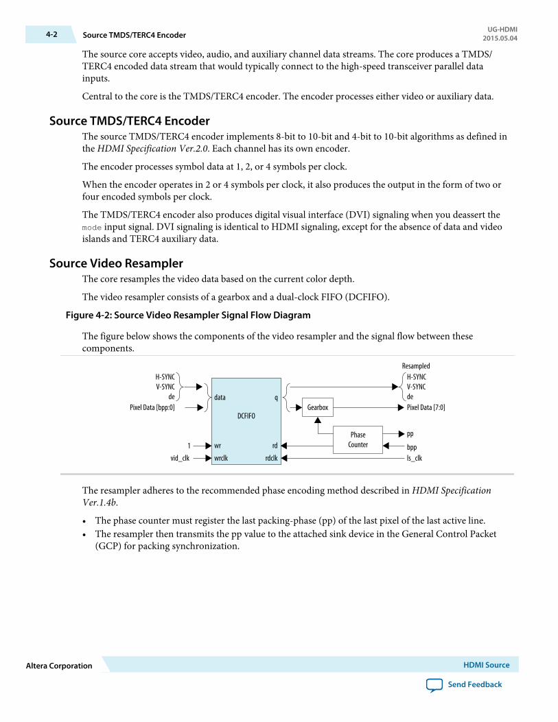
Source Video ResamplerThe core resamples the video data based on the current color depth.
The video resampler consists of a gearbox and a dual-clock FIFO (DCFIFO).
Figure 4-2: Source Video Resampler Signal Flow Diagram
The figure below shows the components of the video resampler and the signal flow between thesecomponents.
Pixel Data [bpp:0]
1
vid_clk
DCFIFO
ls_clk
data
wr
wrclk
q
rd
rdclk
de
H-SYNCV-SYNC
PhaseCounter
Gearbox Pixel Data [7:0]
H-SYNCV-SYNCde
Resampled
pp
bpp
The resampler adheres to the recommended phase encoding method described in HDMI SpecificationVer.1.4b.
• The phase counter must register the last packing-phase (pp) of the last pixel of the last active line.• The resampler then transmits the pp value to the attached sink device in the General Control Packet
(GCP) for packing synchronization.
4-2 Source TMDS/TERC4 EncoderUG-HDMI
2015.05.04
Altera Corporation HDMI Source
Send Feedback
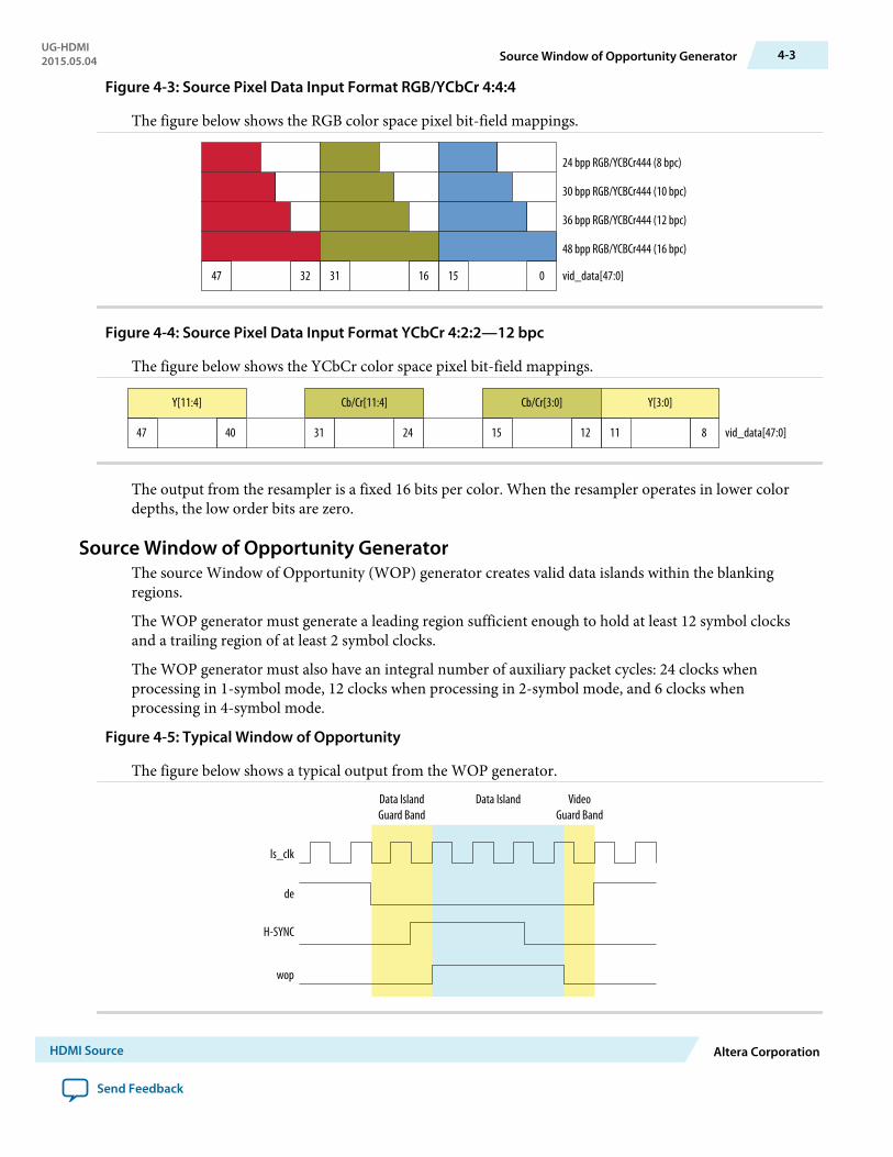
Figure 4-3: Source Pixel Data Input Format RGB/YCbCr 4:4:4
The figure below shows the RGB color space pixel bit-field mappings.
47 32 31 16 15 0 vid_data[47:0]
24 bpp RGB/YCBCr444 (8 bpc)
30 bpp RGB/YCBCr444 (10 bpc)
36 bpp RGB/YCBCr444 (12 bpc)
48 bpp RGB/YCBCr444 (16 bpc)
Figure 4-4: Source Pixel Data Input Format YCbCr 4:2:2—12 bpc
The figure below shows the YCbCr color space pixel bit-field mappings.
31 24 15 12 11 8 vid_data[47:0]47 40
Y[3:0]Cb/Cr[11:4] Cb/Cr[3:0]Y[11:4]
The output from the resampler is a fixed 16 bits per color. When the resampler operates in lower colordepths, the low order bits are zero.
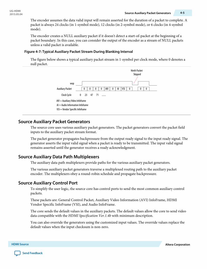
Source Window of Opportunity GeneratorThe source Window of Opportunity (WOP) generator creates valid data islands within the blankingregions.
The WOP generator must generate a leading region sufficient enough to hold at least 12 symbol clocksand a trailing region of at least 2 symbol clocks.
The WOP generator must also have an integral number of auxiliary packet cycles: 24 clocks whenprocessing in 1-symbol mode, 12 clocks when processing in 2-symbol mode, and 6 clocks whenprocessing in 4-symbol mode.
Figure 4-5: Typical Window of Opportunity
The figure below shows a typical output from the WOP generator.
ls_clk
de
H-SYNC
wop
Data IslandGuard Band
VideoGuard Band
Data Island
UG-HDMI2015.05.04 Source Window of Opportunity Generator 4-3
HDMI Source Altera Corporation
Send Feedback

The output from the WOP generator is an aux_de signal propagated backwards through the auxiliarysignal path to provide backpressure.
Based on the HDMI Specification Ver.1.4b requirements, you cannot send more than 9 auxiliary (AUX)packets consecutively during a blanking region. The WOP generator deasserts the data enable line onevery tenth AUX packet to comply with this requirement.
Source Auxiliary Packet EncoderAuxiliary packets are encoded by the source auxiliary packet encoder.
The auxiliary packets originate from a number of sources, which are multiplexed into the auxiliary packetencoder in a round-robin schedule. The auxiliary packet encoder converts a standard stream into thechannel data format required by the TERC4 encoder.
The source propagates the WOP signal backwards through the stream ready signal.
The auxiliary packet encoder also calculates and inserts the Bose-Chaudhuri-Hocquenghem (BCH) errorcorrection code.
Figure 4-6: Auxiliary Packet Encoder Input
The figure below shows the auxiliary packet encoder input from a 72-bit input data.
PB22
PB21
PB15
PB14
PB8
PB7
PB1
PB0
HB0
Phase 0
PB24
PB23
PB17
PB16
PB10
PB9
PB3
PB2
HB1
Phase 1
PB26
PB25
PB19
PB18
PB12
PB11
PB5
PB4
HB2
Phase 2
0
PB27
0
PB20
0
PB13
0
PB6
0
Phase 3
BCH Block 3
BCH Block 2
BCH Block 1
BCH Block 0
Input Data
Byte[8]
Byte[0]
Startofpacket
Endofpacket
Ready
Clock
0 - - 8 - - 16 - - 24Cycle 1 Symbol
0 - - 4 - - 8 - - 12Cycle 2 Symbol
0 - - 2 - - 4 - - 6Cycle 4 Symbol
Phase 0 Phase 1 Phase 2 Phase 3
4-4 Source Auxiliary Packet EncoderUG-HDMI
2015.05.04
Altera Corporation HDMI Source
Send Feedback
The encoder assumes the data valid input will remain asserted for the duration of a packet to complete. Apacket is always 24 clocks (in 1-symbol mode), 12 clocks (in 2-symbol mode), or 6 clocks (in 4-symbolmode).
The encoder creates a NULL auxiliary packet if it doesn't detect a start-of-packet at the beginning of apacket boundary. In this case, you can consider the output of the encoder as a stream of NULL packetsunless a valid packet is available.
Figure 4-7: Typical Auxiliary Packet Stream During Blanking Interval
The figure below shows a typical auxiliary packet stream in 1-symbol per clock mode, where 0 denotes anull packet.
wop
0 0 0 0 AVI 0 AI VSI 0 0 0
0 23 47 71
Auxiliary Packet
Clock Cycle
AVI = Auxiliary Video InfoframeAI = Audio Information InfoframeVSI = Vendor Specific Infoframe
.......
Ninth PacketSkipped
Source Auxiliary Packet GeneratorsThe source core uses various auxiliary packet generators. The packet generators convert the packet fieldinputs to the auxiliary packet stream format.
The packet generator propagates backpressure from the output ready signal to the input ready signal. Thegenerator asserts the input valid signal when a packet is ready to be transmitted. The input valid signalremains asserted until the generator receives a ready acknowledgment.
Source Auxiliary Data Path MultiplexersThe auxiliary data path multiplexers provide paths for the various auxiliary packet generators.
The various auxiliary packet generators traverse a multiplexed routing path to the auxiliary packetencoder. The multiplexers obey a round-robin schedule and propagate backpressure.
Source Auxiliary Control PortTo simplify the user logic, the source core has control ports to send the most common auxiliary controlpackets.
These packets are: General Control Packet, Auxiliary Video Information (AVI) InfoFrame, HDMIVendor Specific InfoFrame (VSI), and Audio InfoFrame.
The core sends the default values in the auxiliary packets. The default values allow the core to send videodata compatible with the HDMI Specification Ver.1.4b with minimum description.
You can also override the generators using the customized input values. The override values replace thedefault values when the input checksum is non-zero.
UG-HDMI2015.05.04 Source Auxiliary Packet Generators 4-5
HDMI Source Altera Corporation
Send Feedback
The core sends the auxiliary control packets on the active edge of the V-SYNC signal to ensure that thepackets are sent once per field.
Source General Control Packet
Table 4-1: Source General Control Packet Input Fields
The table below lists the bit-fields for the Source General Control Packet port.Bit Field Name Comment
gcp[3:0]ColorDepth(CD)
CD3 CD2 CD1 CD0 Color depth (24 bpponly)
0 0 0 0 Color depth notindicated
0 0 0 1 Reserved
0 0 1 0 Reserved
0 0 1 1 Reserved
0 1 0 0 24 bpp
0 1 0 1 30 bpp (1)
0 1 1 0 36 bpp (1)
0 1 1 1 48 bpp (1)
1 1 1 1 Reserved
gcp[4] Set_AVMUTE
Refer to HDMI Specification Ver.1.4b.
gcp[5] Clear_AVMUTE
Refer to HDMI Specification Ver.1.4b.
All other fields for the source GCP are calculated automatically inside the core.
Source Auxiliary Video Information (AVI) InfoFrameThe HDMI core produces the captured AVI InfoFrame to simplify user applications.
Table 4-2: Auxiliary Video Information (AVI) InfoFrame
The table below lists the bit-fields for the AVI InfoFrame port bundle.
The signal bundle is clocked by ls_clk.
Bit-field Name Comment
7:0 Checksum Checksum
9:8 S Scan information
(1) Will be supported in a future release.
4-6 Source General Control PacketUG-HDMI
2015.05.04
Altera Corporation HDMI Source
Send Feedback

Bit-field Name Comment
11:10 B Bar info data valid
12 A0 Active information present
14:13 Y RGB or YCbCr indicator
15 Reserved Returns 0
19:16 R Active format aspect ratio
21:20 M Picture aspect ratio
23:22 C Colorimetry (for example: ITU BT.601, BT.709)
25:24 SC Non-uniform picture scaling
27:26 Q Quantization range
30:28 EC Extended colorimetry
31 ITC IT content
38:32 VIC Video format identification code
39 Reserved Returns 0
43:40 PR Picture repetition factor
45:44 CN Content type
47:46 YQ YCC quantization range
63:48 ETB Line number of end of top bar
79:64 SBB Line number of start of bottom bar
95:80 ELB Pixel number of end of left bar
111:96 SRB Pixel number of start of right bar
112 Disables the core of the InfoFrame packetsfrom inserting.
• 1: The core does not insert info_avi[111:0].
• 0: The core inserts info_avi[111:0]when checksum field (info_avi[7:0]) isnon-zero. The core sends default valueswhen checksum field (info_avi[7:0]) iszero.
Source HDMI Vendor Specific InfoFrame (VSI)The core transmits a HDMI Vendor Specific InfoFrame once per field.
UG-HDMI2015.05.04 Source HDMI Vendor Specific InfoFrame (VSI) 4-7
HDMI Source Altera Corporation
Send Feedback

Table 4-3: HDMI Vendor Specific InfoFrame Bit-Fields
The table below lists the bit-fields for VSI.
The signal bundle is clocked by ls_clk.
Bit-field Name Comment
4:0 Length Length = Nv
12:5 Checksum Checksum
36:13 IEEE 24-bit IEEE registration identified(0×000C03)
41:37 Reserved All 0
44:42 HDMI_Video_Format HDMI video format
52:45 HDMI_VIC HDMI proprietary video formatidentification code
57:53 Reserved All 0
60:58 3D_Ext_Data 3D extended data
61 Disables the core of the InfoFramepackets from inserting.
• 1: The core does not insert info_vsi[60:0].
• 0: The core inserts info_vsi[60:0] when checksum field(info_vsi[12:5]) is non-zero.The core sends default valueswhen checksum field (info_vsi[12:5]) is zero.
Note: If the checksum input to the port is zero, the core uses a default value of zero for each bit-field.
Source Audio InfoFrame (AI)The core transmits an Audio InfoFrame once per field.
Table 4-4: Source Audio InfoFrame Bundle Bit-Fields
The table below lists the signal bit-fields.
The signal bundle is clocked by ls_clk.
Bit-field Name Comment
7:0 Checksum Checksum
10:8 CC Channel count
11 Reserved Returns 0
4-8 Source Audio InfoFrame (AI)UG-HDMI
2015.05.04
Altera Corporation HDMI Source
Send Feedback

Bit-field Name Comment
15:12 CT Audio format type
17:16 SS Bits per audio sample
20:18 SF Sampling frequency
23:21 Reserved Returns 0
31:24 CXT Audio format type of the audiostream
39:32 CA Speaker location allocation FL, FR
41:40 LFEPBL LFE playback level information, dB
42 Reserved Returns 0
46:43 LSV Level shift information, dB
47 DM_INH Down-mix inhibit flag
48 Disables the core of the InfoFramepackets from inserting.
• 1: The core does not insert audio_info_ai[47:0].
• 0: The core inserts audio_info_ai[47:0] when checksum field(audio_info_ai[7:0]) is non-zero. The core sends default valueswhen checksum field (audio_info_ai[7:0]) is zero.
Note: If the checksum input to the port is zero, the core uses a default value of zero for each bit-field.
Source Audio EncoderAudio transport requires three packet types: Audio Timestamp InfoFrame, Audio InformationInfoFrame, and Audio Sample Data.
UG-HDMI2015.05.04 Source Audio Encoder 4-9
HDMI Source Altera Corporation
Send Feedback

Figure 4-8: Source Audio Encoder
TimestampScheduler
Auxiliary PacketGenerator
Auxiliary PacketGenerator
Auxiliary PacketGenerator
CTS, N
Override AI
Audio Input AudioPacketizer
DCFIFO
Default AIV-SYNC
1
Multiplexer
AudioAuxiliaryStream
Audio Data Port
The Audio Timestamp InfoFrame packet contains the CTS and N values. You need to provide thesevalues. The core schedules this packet to be sent every ms. The scheduler uses the ls_clk and CTS valueto determine a 1-ms interval.
The core sends the Audio Information InfoFrame packet on the active edge of the V-SYNC signal.
The Audio Sample Data packet queues on a DCFIFO. The core also uses the DCFIFO to synchronize itsclock to ls_clk. The Audio Packetizer packs the audio sample data into the Audio Sample packets. AnAudio Sample packet can contain up to 4 audio samples, based on the required audio sample clock. Thecore sends the Audio Sample packets whenever there is an available slot in the auxiliary packet stream.
Source ParametersYou set parameters for the source using the Altera HDMI parameter editor.
Table 4-5: HDMI Source Parameters
Parameter Value Description
Device family Stratix V
Arria V
Arria 10
Targeted device family; matches the projectdevice family.
Direction Transmitter = Source
Receiver = Sink
Select HDMI source.
Symbols per clock 1, 2, or 4 symbols perclock
Determines how many TMDS symbols and pixelsare processed per clock.
• Stratix V supports 1 or 2 symbols per clock• Arria V supports 1, 2, or 4 symbols per clock• Arria 10 supports only 2 symbols per clock
4-10 Source ParametersUG-HDMI
2015.05.04
Altera Corporation HDMI Source
Send Feedback
Parameter Value Description
Support auxiliary 0 = No AUX
1 = AUX
Determines if auxiliary channel encoding isincluded.
Support deep color 0 = No deep color
1 = Deep color
Determines if the core can encode deep colorformats.
To enable this parameter, you must also enablethe Support auxiliary parameter.
Note: This parameter is not supported for15.0 release. The parameter always setsto 0.
Support audio 0 = No audio
1 = Audio
Determines if the core can encode audio data.
To enable this parameter, you must also enablethe Support auxiliary parameter.
Support 8-channel audio 0 = No
1 = Yes
Determines if the core can support up to 8 audiochannels. Enable this parameter if you want tosupport more than the default 2 audio channels.
To enable this parameter, you must also enablethe Support audio parameter.
Note: This parameter is not supported for15.0 release. The parameter always setsto 0.
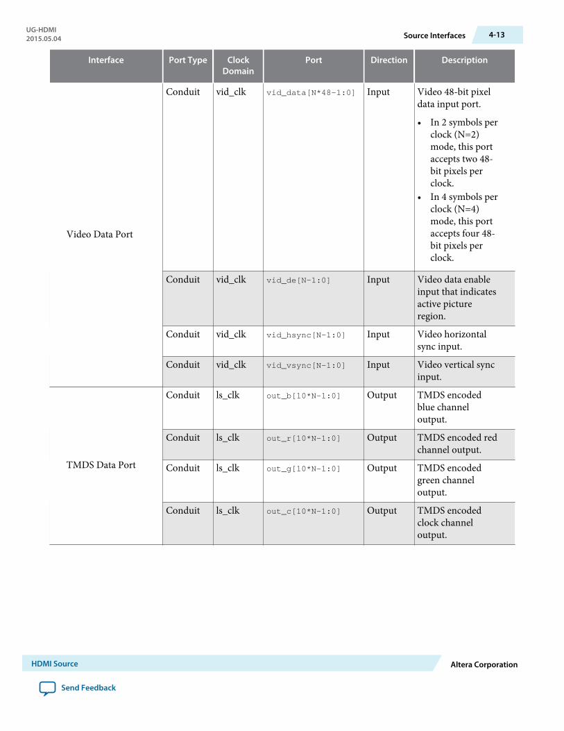
Source InterfacesThe table lists the source's port interfaces.
Table 4-6: Source Interfaces
N is the number of symbols per clock.
Interface Port Type ClockDomain
Port Direction Description
Reset Reset N/A reset Input Main asynchro‐nous reset input.
UG-HDMI2015.05.04 Source Interfaces 4-11
HDMI Source Altera Corporation
Send Feedback

Interface Port Type ClockDomain
Port Direction Description
Clock
Clock N/A ls_clk Input Link speed clockinput.
8/8 (1x), 10/8(1.25x), 12/8 (1.5x),or 16/8 (2x) timesthe vid_clkaccording to colordepth.
This signalconnects to thetransceiver outputclock.
Clock N/A vid_clk Input Video data clockinput.
• 1 symbol perclock mode =video pixelclock
• 2 symbols perclock mode =half the pixelclock
• 4 symbols perclock mode =quarter the pixelclock
Clock N/A audio_clk Input Audio clock input.
4-12 Source InterfacesUG-HDMI
2015.05.04
Altera Corporation HDMI Source
Send Feedback
Interface Port Type ClockDomain
Port Direction Description
Video Data Port
Conduit vid_clk vid_data[N*48-1:0] Input Video 48-bit pixeldata input port.
• In 2 symbols perclock (N=2)mode, this portaccepts two 48-bit pixels perclock.
• In 4 symbols perclock (N=4)mode, this portaccepts four 48-bit pixels perclock.
Conduit vid_clk vid_de[N-1:0] Input Video data enableinput that indicatesactive pictureregion.
Conduit vid_clk vid_hsync[N-1:0] Input Video horizontalsync input.
Conduit vid_clk vid_vsync[N-1:0] Input Video vertical syncinput.
TMDS Data Port
Conduit ls_clk out_b[10*N-1:0] Output TMDS encodedblue channeloutput.
Conduit ls_clk out_r[10*N-1:0] Output TMDS encoded redchannel output.
Conduit ls_clk out_g[10*N-1:0] Output TMDS encodedgreen channeloutput.
Conduit ls_clk out_c[10*N-1:0] Output TMDS encodedclock channeloutput.
UG-HDMI2015.05.04 Source Interfaces 4-13
HDMI Source Altera Corporation
Send Feedback
Interface Port Type ClockDomain
Port Direction Description
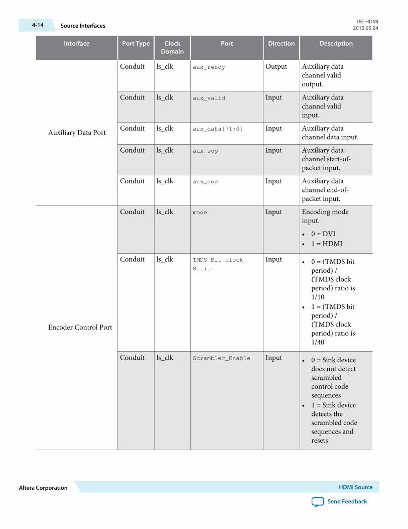
Auxiliary Data Port
Conduit ls_clk aux_ready Output Auxiliary datachannel validoutput.
Conduit ls_clk aux_valid Input Auxiliary datachannel validinput.
Conduit ls_clk aux_data[71:0] Input Auxiliary datachannel data input.
Conduit ls_clk aux_sop Input Auxiliary datachannel start-of-packet input.
Conduit ls_clk aux_eop Input Auxiliary datachannel end-of-packet input.
Encoder Control Port
Conduit ls_clk mode Input Encoding modeinput.
• 0 = DVI• 1 = HDMI
Conduit ls_clk TMDS_Bit_clock_
Ratio
Input • 0 = (TMDS bitperiod) /(TMDS clockperiod) ratio is1/10
• 1 = (TMDS bitperiod) /(TMDS clockperiod) ratio is1/40
Conduit ls_clk Scrambler_Enable Input • 0 = Sink devicedoes not detectscrambledcontrol codesequences
• 1 = Sink devicedetects thescrambled codesequences andresets
4-14 Source InterfacesUG-HDMI
2015.05.04
Altera Corporation HDMI Source
Send Feedback
Interface Port Type ClockDomain
Port Direction Description
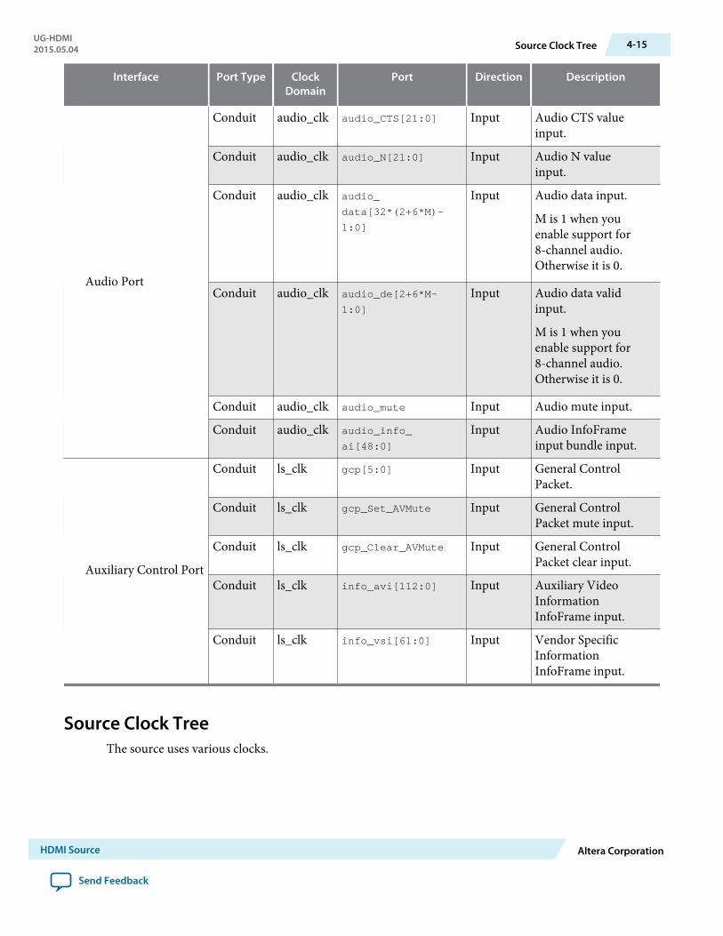
Audio Port
Conduit audio_clk audio_CTS[21:0] Input Audio CTS valueinput.
Conduit audio_clk audio_N[21:0] Input Audio N valueinput.
Conduit audio_clk audio_
data[32*(2+6*M)-
1:0]
Input Audio data input.
M is 1 when youenable support for8-channel audio.Otherwise it is 0.
Conduit audio_clk audio_de[2+6*M-
1:0]
Input Audio data validinput.
M is 1 when youenable support for8-channel audio.Otherwise it is 0.
Conduit audio_clk audio_mute Input Audio mute input.
Conduit audio_clk audio_info_
ai[48:0]
Input Audio InfoFrameinput bundle input.
Auxiliary Control Port
Conduit ls_clk gcp[5:0] Input General ControlPacket.
Conduit ls_clk gcp_Set_AVMute Input General ControlPacket mute input.
Conduit ls_clk gcp_Clear_AVMute Input General ControlPacket clear input.
Conduit ls_clk info_avi[112:0] Input Auxiliary VideoInformationInfoFrame input.
Conduit ls_clk info_vsi[61:0] Input Vendor SpecificInformationInfoFrame input.
Source Clock TreeThe source uses various clocks.
UG-HDMI2015.05.04 Source Clock Tree 4-15
HDMI Source Altera Corporation
Send Feedback

Figure 4-9: Source Clock Tree
The figure shows how the different clocks connect in the source core.
ResamplerFIFO
Sync
TMDS(TERC4)Encoder
Sync
Sync
Sync
HSSI[0]
HSSI[1]
HSSI[2]
HSSI[3]
Transceiver PLL
vid_clk
AUX Data
TransceiverBlockls_clk
Channel[0]
Channel[1]
Channel[2]
TMDS Clock
Pixel Data
WRCLK RDCLK
WRCLK RDCLK
WRCLK RDCLK
WRCLK RDCLK
HDMI Source Core
SwitchGPLL x1.0
x1.25x1.5x2.0
vid_clk
bpp
WRCLK RDCLK
ls_clkvid_clk
The pixel data clocks into the core at the pixel clock (vid_clk). This same clock derives the required linkspeed clock (ls_clk), which is used to drive the transceiver phase-locked loop (PLL) input. The ls_clkdepends on the color bits per pixel (bpp).
For HDMI source, you must instantiate 4 transmitter channels: 3 channels to transmit data and 1 channelto transmit clock information.
You must connect the core ls_clk to the transceiver clock output, which performs the TMDS and TERC4encoding. The auxiliary data clocks into the core at the ls_clk rate.
Related InformationHDMI Hardware Demonstration on page 6-1For more information about the transmitter and receiver channels.
4-16 Source Clock TreeUG-HDMI
2015.05.04
Altera Corporation HDMI Source
Send Feedback

HDMI Sink 52015.05.04
UG-HDMI Subscribe Send Feedback
Sink Functional DescriptionThe HDMI sink core provides direct connection to the Transceiver Native PHY through a 10-bit, 20-bit,or 40-bit parallel data path.
Figure 5-1: HDMI Sink Signal Flow Diagram
The figure below shows the flow of the HDMI sink signals. The figure shows the various clocking domainsused within the core.
VideoResample
AuxiliaryDecoder
AudioDecoder
TMDS TERC4Decoder
AuxiliaryMemory Encoder
Capture AI
Capture AVI
Capture GCP
Color Depth, pp
GCP
AudioData Port
AuxiliaryMemory Interface
AI Infoframe
AVI Infoframe
AUX Data Port
AuxiliaryPacket Capture
ControlPacket Ports
VideoData Port
vid_clk
Video Data
mode
VideoData
AUXData
DeskewWordAlign
Bitslip
reset
Word Alignment and Channel Deskew
TMDSData
ls_clk[2:0]vid_clk[0]ls_clk[0]
Clock Domains
The sink core provides three 10-bit, 20-bit, or 40-bit data input paths corresponding to the color channels.The sink core clocks the three 10-bit, 20-bit, or 40-bit channels from the transceiver outputs using therespective transceiver clock outputs.
• Blue channel: 0• Red channel: 1• Green channel: 2
© 2015 Altera Corporation. All rights reserved. ALTERA, ARRIA, CYCLONE, ENPIRION, MAX, MEGACORE, NIOS, QUARTUS and STRATIX words and logos aretrademarks of Altera Corporation and registered in the U.S. Patent and Trademark Office and in other countries. All other words and logos identified astrademarks or service marks are the property of their respective holders as described at www.altera.com/common/legal.html. Altera warrants performanceof its semiconductor products to current specifications in accordance with Altera's standard warranty, but reserves the right to make changes to anyproducts and services at any time without notice. Altera assumes no responsibility or liability arising out of the application or use of any information,product, or service described herein except as expressly agreed to in writing by Altera. Altera customers are advised to obtain the latest version of devicespecifications before relying on any published information and before placing orders for products or services.
ISO9001:2008Registered
www.altera.com101 Innovation Drive, San Jose, CA 95134

Sink Channel Word Alignment and DeskewThe input stage of the sink is responsible for synchronizing the incoming parallel data channels correctly.The synchronization is split to two stages: word alignment and channel deskew.
Word alignment • Correctly aligns the incoming parallel data to word boundaries usingbit-slip technique.
• TMDS encoding does not guarantee unique control codes, but the corecan still use the sequence of continuous symbols found in data andvideo preambles to align.
• The alignment algorithm searches for 12 consecutive 0×54 or 0×abcorresponding to the data and video preambles.
Note: The preambles are also present in digital video interface(DVI) coding.
• The alignment logic asserts a marker indicator when the 12 consecu‐tive signals are detected.
• Similarly, the logic infers alignment loss when 8K symbol clocks elapsewithout a single marker assertion.
Channel deskew • When the data channels are aligned, the core then attempts to deskeweach channel.
• The sink core deskews at the rising edge of the marker insertion.• For every correct deskewed lane, the marker insertion will appear in all
three TMDS encoded streams.• The sink core deskews using three dual-clock FIFOs.• The dual-clock FIFOs also synchronize all three data streams to the
blue channel clock to be used later throughout the decoder core.
5-2 Sink Channel Word Alignment and DeskewUG-HDMI
2015.05.04
Altera Corporation HDMI Sink
Send Feedback
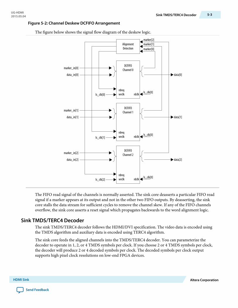
Figure 5-2: Channel Deskew DCFIFO Arrangement
The figure below shows the signal flow diagram of the deskew logic.
AlignmentDetection
DCFIFOChannel 0
rdreqwrclk rdclk
DCFIFOChannel 1
rdreqwrclk rdclk
DCFIFOChannel 2
rdreqwrclk rdclk
ls_clk[0]
ls_clk[0]
ls_clk[0]ls_clk[2]
ls_clk[1]
ls_clk[0]
marker_in[0]
data_in[0] data[0]
marker_in[1]
data_in[1] data[1]
marker_in[2]
data_in[2] data[2]
marker[2]marker[1]marker[0]
The FIFO read signal of the channels is normally asserted. The sink core deasserts a particular FIFO readsignal if a marker appears at its output and not in the other two FIFO outputs. By deasserting, the sinkcore stalls the data stream for sufficient cycles to remove the channel skew. If any of the FIFO channelsoverflow, the sink core asserts a reset signal which propagates backwards to the word alignment logic.
Sink TMDS/TERC4 DecoderThe sink TMDS/TERC4 decoder follows the HDMI/DVI specification. The video data is encoded usingthe TMDS algorithm and auxiliary data is encoded using TERC4 algorithm.
The sink core feeds the aligned channels into the TMDS/TERC4 decoder. You can parameterize thedecoder to operate in 1, 2, or 4 TMDS symbols per clock. If you choose 2 or 4 TMDS symbols per clock,the decoder will produce 2 or 4 decoded symbols per clock. The decoded symbols per clock outputsupports high pixel clock resolutions on low-end FPGA devices.
UG-HDMI2015.05.04 Sink TMDS/TERC4 Decoder 5-3
HDMI Sink Altera Corporation
Send Feedback

Sink Video ResamplerThe video resampler consists of a gearbox and a dual-clock FIFO (DCFIFO).
The gearbox converts 8 bit-per-second (bps) data to 8-, 10-, 12- or 16-bps data based on the current colordepth. The GCP conveys the color depth information.
Figure 5-3: Sink Resampler Signal Flow Diagram
H-SYNCV-SYNCde
Pixel Data [bpp:0]
1
vid_clk
DCFIFO
ls_clk
q
rd
rdwrclk
data
wr
wrclk
PhaseCounter
Gearbox
H-SYNCV-SYNC
dePixel Data [7:0]
Resampled
pp
bpp
The resampler adheres to the recommended phase count method described in HDMI Specification Ver.1.4b.
• To keep the source and sink resamples synchronized, the source must send the phase-packing (pp)value to the sink during the vertical blanking phase, using the general control packet.
• The pp corresponds to the phase of the last pixel in the last active video line.• The phase-counter logic compares its own pp value to the pp value received in the general control
packet and slips the phase count if the two pp values do not agree.
The output from the resampler is a fixed 16 bits per color. When the resampler operates in lower colordepths, the low order bits are zero.
Sink Auxiliary Decoder
The sink core decodes the auxiliary data path into a 72-bit wide standard packet stream. The streamcontains a valid, start-of-packet (SOP) and end-of-packet (EOP) marker.
5-4 Sink Video ResamplerUG-HDMI
2015.05.04
Altera Corporation HDMI Sink
Send Feedback
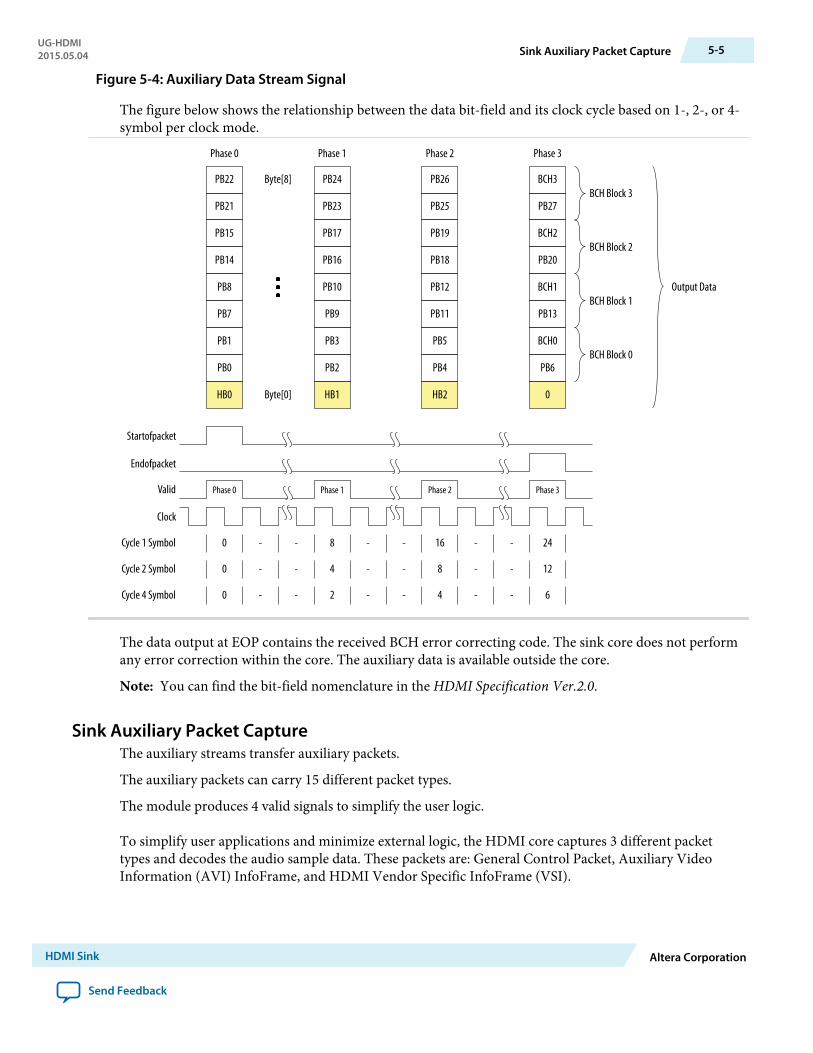
Figure 5-4: Auxiliary Data Stream Signal
The figure below shows the relationship between the data bit-field and its clock cycle based on 1-, 2-, or 4-symbol per clock mode.
PB22
PB21
PB15
PB14
PB8
PB7
PB1
PB0
HB0
Phase 0
PB24
PB23
PB17
PB16
PB10
PB9
PB3
PB2
HB1
Phase 1
PB26
PB25
PB19
PB18
PB12
PB11
PB5
PB4
HB2
Phase 2
BCH3
PB27
BCH2
PB20
BCH1
PB13
BCH0
PB6
0
Phase 3
BCH Block 3
BCH Block 2
BCH Block 1
BCH Block 0
Output Data
Byte[8]
Byte[0]
Startofpacket
Endofpacket
Valid
Clock
0 - - 8 - - 16 - - 24Cycle 1 Symbol
0 - - 4 - - 8 - - 12Cycle 2 Symbol
0 - - 2 - - 4 - - 6Cycle 4 Symbol
Phase 0 Phase 1 Phase 2 Phase 3
The data output at EOP contains the received BCH error correcting code. The sink core does not performany error correction within the core. The auxiliary data is available outside the core.
Note: You can find the bit-field nomenclature in the HDMI Specification Ver.2.0.
Sink Auxiliary Packet CaptureThe auxiliary streams transfer auxiliary packets.
The auxiliary packets can carry 15 different packet types.
The module produces 4 valid signals to simplify the user logic.
To simplify user applications and minimize external logic, the HDMI core captures 3 different packettypes and decodes the audio sample data. These packets are: General Control Packet, Auxiliary VideoInformation (AVI) InfoFrame, and HDMI Vendor Specific InfoFrame (VSI).
UG-HDMI2015.05.04 Sink Auxiliary Packet Capture 5-5
HDMI Sink Altera Corporation
Send Feedback
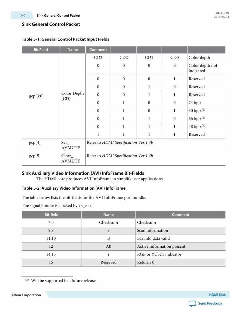
Sink General Control Packet
Table 5-1: General Control Packet Input Fields
Bit Field Name Comment
gcp[3:0] Color Depth(CD)
CD3 CD2 CD1 CD0 Color depth
0 0 0 0 Color depth notindicated
0 0 0 1 Reserved
0 0 1 0 Reserved
0 0 1 1 Reserved
0 1 0 0 24 bpp
0 1 0 1 30 bpp (2)
0 1 1 0 36 bpp (2)
0 1 1 1 48 bpp (2)
1 1 1 1 Reserved
gcp[4] Set_AVMUTE
Refer to HDMI Specification Ver.1.4b
gcp[5] Clear_AVMUTE
Refer to HDMI Specification Ver.1.4b
Sink Auxiliary Video Information (AVI) InfoFrame Bit-FieldsThe HDMI core produces AVI InfoFrame to simplify user applications.
Table 5-2: Auxiliary Video Information (AVI) InfoFrame
The table below lists the bit-fields for the AVI InfoFrame port bundle.
The signal bundle is clocked by ls_clk.
Bit-field Name Comment
7:0 Checksum Checksum
9:8 S Scan information
11:10 B Bar info data valid
12 A0 Active information present
14:13 Y RGB or YCbCr indicator
15 Reserved Returns 0
(2) Will be supported in a future release.
5-6 Sink General Control PacketUG-HDMI
2015.05.04
Altera Corporation HDMI Sink
Send Feedback

Bit-field Name Comment
19:16 R Active format aspect ratio
21:20 M Picture aspect ratio
23:22 C Colorimetry (for example: ITU BT.601, BT.709)
25:24 SC Non-uniform picture scaling
27:26 Q Quantization range
30:28 EC Extended colorimetry
31 ITC IT content
38:32 VIC Video format identification code
39 Reserved Returns 0
43:40 PR Picture repetition factor
45:44 CN Content type
47:46 YQ YCC quantization range
63;48 ETB Line number of end of top bar
79:64 SBB Line number of start of bottom bar
95:80 ELB Pixel number of end of left bar
111:96 SRB Pixel number of start of right bar
Sink HDMI Vendor Specific InfoFrame (VSI)The core produces the captured HDMI Vendor Specific InfoFrame to simplify user applications.
Table 5-3: HDMI Vendor Specific InfoFrame Bit-Fields
The table below lists the bit-fields for VSI.
The signal bundle is clocked by ls_clk.
Bit-field Name Comment
4:0 Length Length = Nv
12:5 Checksum Checksum
36:13 IEEE 24-bit IEEE registration identified(0x000C03)
41:37 Reserved All 0
44:42 HDMI_Video_Format HDMI video format
52:45 HDMI_VIC HDMI proprietary video formatidentification code
57:53 Reserved All 0
UG-HDMI2015.05.04 Sink HDMI Vendor Specific InfoFrame (VSI) 5-7
HDMI Sink Altera Corporation
Send Feedback
Bit-field Name Comment
60:58 3D_Ext_Data 3D extended data
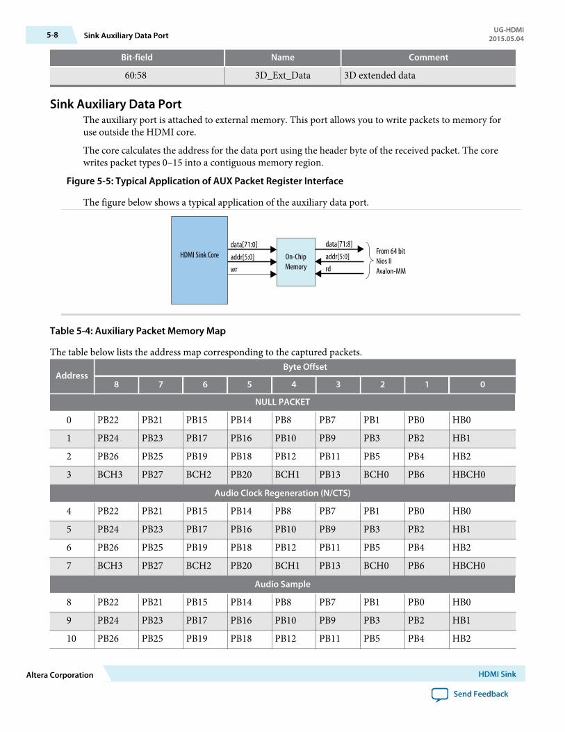
Sink Auxiliary Data PortThe auxiliary port is attached to external memory. This port allows you to write packets to memory foruse outside the HDMI core.
The core calculates the address for the data port using the header byte of the received packet. The corewrites packet types 0–15 into a contiguous memory region.
Figure 5-5: Typical Application of AUX Packet Register Interface
The figure below shows a typical application of the auxiliary data port.
data[71:0]HDMI Sink Core
wraddr[5:0] On-Chip
Memory
data[71:8]
rdaddr[5:0]
From 64 bitNios IIAvalon-MM
Table 5-4: Auxiliary Packet Memory Map
The table below lists the address map corresponding to the captured packets.
AddressByte Offset
8 7 6 5 4 3 2 1 0
NULL PACKET
0 PB22 PB21 PB15 PB14 PB8 PB7 PB1 PB0 HB0
1 PB24 PB23 PB17 PB16 PB10 PB9 PB3 PB2 HB1
2 PB26 PB25 PB19 PB18 PB12 PB11 PB5 PB4 HB2
3 BCH3 PB27 BCH2 PB20 BCH1 PB13 BCH0 PB6 HBCH0
Audio Clock Regeneration (N/CTS)
4 PB22 PB21 PB15 PB14 PB8 PB7 PB1 PB0 HB0
5 PB24 PB23 PB17 PB16 PB10 PB9 PB3 PB2 HB1
6 PB26 PB25 PB19 PB18 PB12 PB11 PB5 PB4 HB2
7 BCH3 PB27 BCH2 PB20 BCH1 PB13 BCH0 PB6 HBCH0
Audio Sample
8 PB22 PB21 PB15 PB14 PB8 PB7 PB1 PB0 HB0
9 PB24 PB23 PB17 PB16 PB10 PB9 PB3 PB2 HB1
10 PB26 PB25 PB19 PB18 PB12 PB11 PB5 PB4 HB2
5-8 Sink Auxiliary Data PortUG-HDMI
2015.05.04
Altera Corporation HDMI Sink
Send Feedback

Audio Sample
11 BCH3 PB27 BCH2 PB20 BCH1 PB13 BCH0 PB6 HBCH0
General Control
12 PB22 PB21 PB15 PB14 PB8 PB7 PB1 PB0 HB0
13 PB24 PB23 PB17 PB16 PB10 PB9 PB3 PB2 HB1
14 PB26 PB25 PB19 PB18 PB12 PB11 PB5 PB4 HB2
15 BCH3 PB27 BCH2 PB20 BCH1 PB13 BCH0 PB6 HBCH0
ACP Packet
16 PB22 PB21 PB15 PB14 PB8 PB7 PB1 PB0 HB0
17 PB24 PB23 PB17 PB16 PB10 PB9 PB3 PB2 HB1
18 PB26 PB25 PB19 PB18 PB12 PB11 PB5 PB4 HB2
19 BCH3 PB27 BCH2 PB20 BCH1 PB13 BCH0 PB6 HBCH0
ISRC1 Packet
20 PB22 PB21 PB15 PB14 PB8 PB7 PB1 PB0 HB0
21 PB24 PB23 PB17 PB16 PB10 PB9 PB3 PB2 HB1
22 PB26 PB25 PB19 PB18 PB12 PB11 PB5 PB4 HB2
23 BCH3 PB27 BCH2 PB20 BCH1 PB13 BCH0 PB6 HBCH0
ISRC2 Packet
24 PB22 PB21 PB15 PB14 PB8 PB7 PB1 PB0 HB0
25 PB24 PB23 PB17 PB16 PB10 PB9 PB3 PB2 HB1
26 PB26 PB25 PB19 PB18 PB12 PB11 PB5 PB4 HB2
27 BCH3 PB27 BCH2 PB20 BCH1 PB13 BCH0 PB6 HBCH0
One Bit Audio Sample Packet 5.3.9
28 PB22 PB21 PB15 PB14 PB8 PB7 PB1 PB0 HB0
29 PB24 PB23 PB17 PB16 PB10 PB9 PB3 PB2 HB1
30 PB26 PB25 PB19 PB18 PB12 PB11 PB5 PB4 HB2
31 BCH3 PB27 BCH2 PB20 BCH1 PB13 BCH0 PB6 HBCH0
DST Audio Packet
32 PB22 PB21 PB15 PB14 PB8 PB7 PB1 PB0 HB0
33 PB24 PB23 PB17 PB16 PB10 PB9 PB3 PB2 HB1
34 PB26 PB25 PB19 PB18 PB12 PB11 PB5 PB4 HB2
35 BCH3 PB27 BCH2 PB20 BCH1 PB13 BCH0 PB6 HBCH0
UG-HDMI2015.05.04 Sink Auxiliary Data Port 5-9
HDMI Sink Altera Corporation
Send Feedback
High Bitrate (HBR) Audio Stream Packet
36 PB22 PB21 PB15 PB14 PB8 PB7 PB1 PB0 HB0
37 PB24 PB23 PB17 PB16 PB10 PB9 PB3 PB2 HB1
38 PB26 PB25 PB19 PB18 PB12 PB11 PB5 PB4 HB2
39 BCH3 PB27 BCH2 PB20 BCH1 PB13 BCH0 PB6 HBCH0
Gamut Metadata Packet
40 PB22 PB21 PB15 PB14 PB8 PB7 PB1 PB0 HB0
41 PB24 PB23 PB17 PB16 PB10 PB9 PB3 PB2 HB1
42 PB26 PB25 PB19 PB18 PB12 PB11 PB5 PB4 HB2
43 BCH3 PB27 BCH2 PB20 BCH1 PB13 BCH0 PB6 HBCH0
Vendor-Specific InfoFrame
44 PB22 PB21 PB15 PB14 PB8 PB7 PB1 PB0 HB0
45 PB24 PB23 PB17 PB16 PB10 PB9 PB3 PB2 HB1
46 PB26 PB25 PB19 PB18 PB12 PB11 PB5 PB4 HB2
47 BCH3 PB27 BCH2 PB20 BCH1 PB13 BCH0 PB6 HBCH0
AVI InfoFrame
48 PB22 PB21 PB15 PB14 PB8 PB7 PB1 PB0 HB0
49 PB24 PB23 PB17 PB16 PB10 PB9 PB3 PB2 HB1
50 PB26 PB25 PB19 PB18 PB12 PB11 PB5 PB4 HB2
51 BCH3 PB27 BCH2 PB20 BCH1 PB13 BCH0 PB6 HBCH0
Source Product Descriptor InfoFrame
52 PB22 PB21 PB15 PB14 PB8 PB7 PB1 PB0 HB0
53 PB24 PB23 PB17 PB16 PB10 PB9 PB3 PB2 HB1
54 PB26 PB25 PB19 PB18 PB12 PB11 PB5 PB4 HB2
55 BCH3 PB27 BCH2 PB20 BCH1 PB13 BCH0 PB6 HBCH0
Audio InfoFrame
56 PB22 PB21 PB15 PB14 PB8 PB7 PB1 PB0 HB0
57 PB24 PB23 PB17 PB16 PB10 PB9 PB3 PB2 HB1
58 PB26 PB25 PB19 PB18 PB12 PB11 PB5 PB4 HB2
59 BCH3 PB27 BCH2 PB20 BCH1 PB13 BCH0 PB6 HBCH0
MPEG Source InfoFrame
60 PB22 PB21 PB15 PB14 PB8 PB7 PB1 PB0 HB0
5-10 Sink Auxiliary Data PortUG-HDMI
2015.05.04
Altera Corporation HDMI Sink
Send Feedback

MPEG Source InfoFrame
61 PB24 PB23 PB17 PB16 PB10 PB9 PB3 PB2 HB1
62 PB26 PB25 PB19 PB18 PB12 PB11 PB5 PB4 HB2
63 BCH3 PB27 BCH2 PB20 BCH1 PB13 BCH0 PB6 HBCH0
Sink Audio DecodingThe sink core sends the audio data using auxiliary packets. You can use three packet types in transportingaudio: Audio InfoFrame, Audio Timestamp, and Audio Sample Data.
The Audio InfoFrame packet is not used within the core but it is captured and presented outside the core.
The Audio Timestamp packet transmits the CTS and N values required to synthesize the audio sampleclock. The core also makes the CTS and N values available outside the core. The audio clock synthesizeruses a phase-counter to recover the audio sample rate.
Figure 5-6: Audio Decoder Signal Flow
Capture AudioInfoFrame
Capture AudioTimestamp
AudioDepacketizer
Valid
AudioSample
FIFO
Audio ClockSynthesizer
wr
AuxiliaryStreamPackets
Audio Data
data
rd
q
CTS, N
AI InfoFrame
Audio Valid
Audio LPCM
The output from the audio clock synthesizer generates a valid pulse at the same rate as the audio sampleclock used in the HDMI source device. This valid pulse is available outside the core as an audio samplevalid signal. This signal reads from a FIFO, which governs the rate of audio samples. The audio depacke‐tizer drives the input to the FIFO.
The audio depacketizer extracts the 32-bit audio sample data from the incoming Audio Sample packets.The Audio Sample packets can hold from one to four sample data values.
Sink ParametersYou set parameters for the sink using the Altera HDMI parameter editor.
Table 5-5: HDMI Sink Parameters
Parameter Value Description
Device family Stratix V
Arria V
Arria 10
Targeted device family; matches the projectdevice family.
UG-HDMI2015.05.04 Sink Audio Decoding 5-11
HDMI Sink Altera Corporation
Send Feedback
Parameter Value Description
Direction Transmitter = Source
Receiver = Sink
Select HDMI sink.
Symbols per clock 1, 2, or 4 symbols perclock
Determines how many TMDS symbols and pixelsare processed per clock.
• Stratix V supports 1 or 2 symbols per clock• Arria V supports 1, 2, or 4 symbols per clock• Arria 10 supports only 2 symbols per clock
Support auxiliary 0 = No AUX
1 = AUX
Determines if auxiliary channel encoding isincluded.
Support deep color 0 = No deep color
1 = Deep color
Determines if the core can encode deep colorformats.
To enable this parameter, you must also enablethe Support auxiliary parameter.
Note: This parameter is not supported for15.0 release. The parameter will alwaysset to 0.
Support audio 0 = No audio
1 = Audio
Determines if the core can encode audio data.
To enable this parameter, you must also enablethe Support auxiliary parameter.
Support 8-channel audio 0 = No
1 = Yes
Determines if the core can support up to 8 audiochannels. Enable this parameter if you want tosupport more than the default 2 audio channels.
To enable this parameter, you must also enablethe Support audio parameter.
Note: This parameter is not supported for15.0 release. The parameter will alwaysset to 0.
Sink InterfacesThe table lists the sink's port interfaces.
5-12 Sink InterfacesUG-HDMI
2015.05.04
Altera Corporation HDMI Sink
Send Feedback
Table 5-6: Sink Interfaces
N is the number of symbols per clock.
Interface Port Type ClockDomain
Port Direction Description
Reset Reset N/A reset Input Main asynchro‐nous reset input.
Note: Resettingthe inputwill resettheSCDCregister.
Clock
Clock N/A ls_clk[2:0] Input Link speed clockinput.
These clockscorrespond to thein_r, in_g, andin_b TMDSencoded datainputs.
Clock N/A vid_clk Input Video data clockinput.
Typically, 8/8, 8/10,8/12, 8/16 times thels_clk accordingto color depth (seeGeneral ControlPacket output).
UG-HDMI2015.05.04 Sink Interfaces 5-13
HDMI Sink Altera Corporation
Send Feedback
Interface Port Type ClockDomain
Port Direction Description
Video Data Port
Conduit vid_clk vid_data[N*48-1:0] Output Video 48-bit pixeldata output port.
In 2 symbols perclock (N=2) mode,this port producestwo 48-bit pixelsper clock.
In 4 symbols perclock (N=4) mode,this port producesfour 48-bit pixelsper clock.
Conduit vid_clk vid_de[N-1:0] Output Video data enableoutput thatindicates activepicture region.
Conduit vid_clk vid_hsync[N-1:0] Output Video horizontalsync output.
Conduit vid_clk vid_vsync[N-1:0] Output Video vertical syncoutput.
Conduit vid_clk locked[2:0] Output Indicates that theHDMI sink core islocked to theTMDS signals.
Each bit representsa color channel.
5-14 Sink InterfacesUG-HDMI
2015.05.04
Altera Corporation HDMI Sink
Send Feedback
Interface Port Type ClockDomain
Port Direction Description
TMDS Data Port
Conduit ls_clk[0] in_b[N*10-1:0] Input TMDS encodedblue channel input.
Conduit ls_clk[1] in_r[N*10-1:0] Input TMDS encoded redchannel input.
Conduit ls_clk[2] in_g[N*10-1:0] Input TMDS encodedgreen channelinput.
Conduit ls_clk[2:0] in_lock[2:0] Input Ready signal fromthe transceiverreset controller thatindicates thetransceivers arelocked.
Each bit representsa color channel.
Auxiliary Data Port
Conduit ls_clk[0] aux_valid Output Auxiliary datachannel validoutput.
Conduit ls_clk[0] aux_data[71:0] Output Auxiliary datachannel dataoutput.
Conduit ls_clk[0] aux_sop Output Auxiliary datachannel start-of-packet input.
Conduit ls_clk[0] aux_eop Output Auxiliary datachannel end-of-packet output.
Decoder Control Port Conduit ls_clk[0] TMDS_Bit_clock_
Ratio
Output • 0 = (TMDS bitperiod) /(TMDS clockperiod) ratio is1/10
• 1 = (TMDS bitperiod) /(TMDS clockperiod) ratio is1/40
UG-HDMI2015.05.04 Sink Interfaces 5-15
HDMI Sink Altera Corporation
Send Feedback

Interface Port Type ClockDomain
Port Direction Description
Audio Port
Conduit ls_clk[0] audio_CTS[21:0] Output Audio CTS valueoutput.
Conduit ls_clk[0] audio_N[21:0] Output Audio N valueoutput.
Conduit ls_clk[0] audio_
data[32*(2+6*M)-
1:0]
Output Audio data output.
M is 1 when youenable support for8-channel audio.Otherwise it is 0.
Conduit ls_clk[0] audio_valid[2+6*M-
1:0]
Output Audio data validoutput.
M is 1 when youenable support for8-channel audio.Otherwise it is 0.
Conduit ls_clk[0] audio_info_
ai[47:0]
Input Audio infoFrameinput bundle.
Auxiliary MemoryInterface
Conduit ls_clk[0] aux_pkt_addr[5:0] Output Auxiliary packetmemory bufferaddress output.
Conduit ls_clk[0] aux_pkt_data[71:0] Output Auxiliary packetmemory bufferdata output.
Conduit ls_clk[0] aux_pkt_wr Output Auxiliary packetmemory bufferwrite strobe output.
5-16 Sink InterfacesUG-HDMI
2015.05.04
Altera Corporation HDMI Sink
Send Feedback

Interface Port Type ClockDomain
Port Direction Description
Auxiliary Control Port
Conduit ls_clk[0] gcp[5:0] Output General ControlPacket output.
Conduit ls_clk[0] gcp_Set_AVMute Output General ControlPacket muteoutput.
Conduit ls_clk[0] gcp_Clear_AVMute Output General ControlPacket clear output.
Conduit ls_clk[0] info_avi[111:0] Output Auxiliary VideoInformationInfoFrame output.
Conduit ls_clk[0] info_vsi[60:0] Output Vendor SpecificInformationInfoFrame output.
Avalon-MM SCDC Management Interface
Table 5-7: Avalon-MM Status and Control Data Channel (SCDC) Management Interface Signals
The table lists the Avalon Memory-Mapped (Avalon-MM) Status and Control Data Channel (SCDC)Management interface signals.
Signal Direction Description
scdc_i2c_clk Input Avalon-MM clock input.
scdc_i2c_addr[7:0] Input 8-bit Avalon-MM address.
scdc_i2c_r Input Read signal.
scdc_i2c_rdata[31:0] Output Output data.
scdc_i2c_w Input Write signal.
scdc_i2c_wdata[31:0] Input Input data.
For more information about SCDC, refer to the HDMI 2.0 Specification Section 10.4 (Status and ControlData Channel).
Sink Clock TreeThe sink core uses different clocks.
The logic clocks the transceiver data into the core using the three CDR clocks: (ls_clk[2:0]).
The TMDS and TERC4 decoding is done at the link-speed clock. The sink then resamples the pixel dataand presents the data at the output of the core at the video pixel clock (vid_clk).
The pixel data clock depends on the video format used (within HDMI specification).
UG-HDMI2015.05.04 Avalon-MM SCDC Management Interface 5-17
HDMI Sink Altera Corporation
Send Feedback

• 8-bpp—link speed clock divided by 1• 10-bpp—link speed clock divided by 1.25• 12-bpp—link speed clock divided by 1.5• 16-bpp—link speed clock divided by 2
For HDMI sink, you need to instantiate 3 receiver channels to receive data.
Figure 5-7: Sink Clock Tree
The figure shows how the different clocks can be selected for the sink core.
ResamplerFIFO
Sync
TMDS(TERC4)Decoder
Sync
Sync
HSSI[0]
HSSI[1]
HSSI[2]
AUX Data
TransceiverBlock ls_clk[0]
Channel[0]
Channel[1]
Channel[2]
Video Data
RDCLKWRCLK
RDCLKWRCLK
RDCLKWRCLK
HDMI Sink Core
WRCLK
RDCLK
SwitchGPLL /1.0
/1.25/1.5/2.0
TMDS Clock
bpp
vid_clk
ls_clk[1]
ls_clk[2]
ls_clk
TMDS clockvid_clk
Related InformationHDMI Hardware Demonstration on page 6-1For more information about the transmitter and receiver channels.
5-18 Sink Clock TreeUG-HDMI
2015.05.04
Altera Corporation HDMI Sink
Send Feedback
HDMI Hardware Demonstration 62015.05.04
UG-HDMI Subscribe Send Feedback
The Altera High-Definition Multimedia Interface (HDMI) hardware demonstration allows you toevaluate the functionality of the HDMI IP core and provides a starting point for you to create your owndesign.
The demonstration runs on both Arria V GX starter board and Stratix V GX development board.
• For HDMI 2.0 design, use Bitec HDMI 2.0 HSMC daughter card revision 1.• For HDMI 1.4b design, use Bitec HDMI 1.4b HSMC daughter card revision 2.
The designs perform a direct pass-through for a standard HDMI video stream.
Note: If you want to use another board or daughter card, check the schematics and change the pinassignments accordingly.
The HDMI 1.4b design also instantiates the following Video and Image Processing (VIP) Suite IP cores:
• Clocked Video Input (CVI)• Clocked Video Output (CVO)• Frame Buffer
The HDMI 2.0 desgin replaces the CVI, CVO and Frame Buffer IP cores with a FIFO buffer between thereceiver and transmitter paths.
© 2015 Altera Corporation. All rights reserved. ALTERA, ARRIA, CYCLONE, ENPIRION, MAX, MEGACORE, NIOS, QUARTUS and STRATIX words and logos aretrademarks of Altera Corporation and registered in the U.S. Patent and Trademark Office and in other countries. All other words and logos identified astrademarks or service marks are the property of their respective holders as described at www.altera.com/common/legal.html. Altera warrants performanceof its semiconductor products to current specifications in accordance with Altera's standard warranty, but reserves the right to make changes to anyproducts and services at any time without notice. Altera assumes no responsibility or liability arising out of the application or use of any information,product, or service described herein except as expressly agreed to in writing by Altera. Altera customers are advised to obtain the latest version of devicespecifications before relying on any published information and before placing orders for products or services.
ISO9001:2008Registered
www.altera.com101 Innovation Drive, San Jose, CA 95134

Figure 6-1: HDMI Hardware Demonstration Block Diagram
The figure below shows a high level block diagram of the demonstration.
Reconfiguration ManagementState Machine
ALTPLLReconfiguration (RX)
GPLL (RX)
GXB (RX) HDMI (RX) Top
Altera TransceiverReconfiguration
Nios II
Frame BufferCVI CVO
WatchdogTimer
ALTPLLReconfiguration (TX)
GPLL (TX)
GXB (TX)HDMI (TX) Top
ALTPLL(SYS_PLL)
VIP Pass-through Qsys System
HDMI RX Group Logic
HDMI TX Group Logic
DataControlClock
Note: The Arria V GX design has an additional SYS_PLL component to generate clock supply to thetransceiver PLL and the HDMI PLL.
HDMI Hardware Demonstration RequirementsThe HDMI demonstration requires an Altera FPGA board and supporting hardware.
• Arria V GX FPGA Starter Kit or Stratix V GX FPGA Development Kit• Bitec HDMI 2.0 HSMC daughter card version 1 (for HDMI 2.0 design) or Bitec HDMI 1.4b HSMC
daughter card version 2 (for HDMI 1.4b design)• PC with a HDMI output• Monitor with a HDMI input• 2 HDMI cables
• A cable to connect the graphics card to the Bitec daughter card RX connector.• A cable to connect the Bitec daughter card TX connector to the monitor.
Note: Altera recommends that you test the PC and monitor first by connecting the PC directly to themonitor. This ensures all the drivers are installed correctly.
The Bitec HDMI HSMC daughter card is designed to allow the Arria V GX or Stratix V GX FPGA deviceto interface with the HDMI source and sink devices.
The following figures illustrate schematic diagram of the Bitec HDMI 1.4b and HSMC Bitec HDMI 2.0HSMC daughter cards.
6-2 HDMI Hardware Demonstration RequirementsUG-HDMI
2015.05.04
Altera Corporation HDMI Hardware Demonstration
Send Feedback
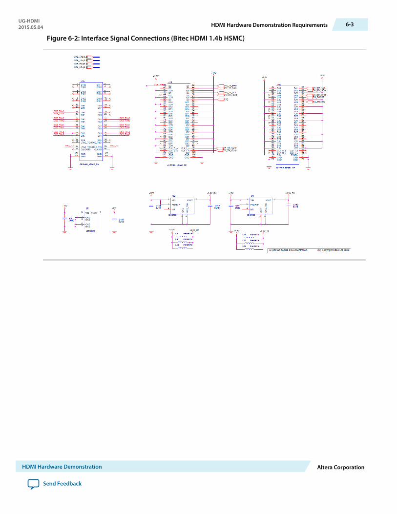
Figure 6-2: Interface Signal Connections (Bitec HDMI 1.4b HSMC)
UG-HDMI2015.05.04 HDMI Hardware Demonstration Requirements 6-3
HDMI Hardware Demonstration Altera Corporation
Send Feedback
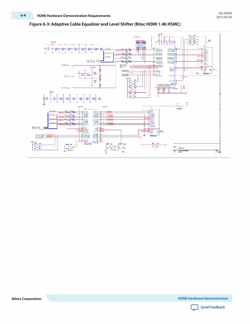
Figure 6-3: Adaptive Cable Equalizer and Level Shifter (Bitec HDMI 1.4b HSMC)
6-4 HDMI Hardware Demonstration RequirementsUG-HDMI
2015.05.04
Altera Corporation HDMI Hardware Demonstration
Send Feedback

Figure 6-4: Interface Signal Connections (Bitec HDMI 2.0 HSMC)
UG-HDMI2015.05.04 HDMI Hardware Demonstration Requirements 6-5
HDMI Hardware Demonstration Altera Corporation
Send Feedback

Figure 6-5: Adaptive Cable Equalizer and Level Shifter (Bitec HDMI 2.0 HSMC)
Related Information
• Arria V GX Starter Kit User Guide• Stratix V GX FPGA Development Kit User Guide
Transceiver and Clocking ConfigurationThe Arria V demonstration uses 2 symbols per clock for HDMI 1.4b design and 4 symbols per clock forHDMI 2.0 design. The Stratix V demonstration uses 2 symbols per clock for HDMI 1.4b and 2.0 designs.
6-6 Transceiver and Clocking ConfigurationUG-HDMI
2015.05.04
Altera Corporation HDMI Hardware Demonstration
Send Feedback

Table 6-1: Tranceiver Configuration Settings
ParametersSettings
Receiver Transmitter
Datapath Options
Enable TX datapath Off On
Enable RX datapath On Off
Enable standard PCS On On
Number of data channels 3 4
Enable simplified datainterface
On On
RX PMA
Data rate 3000 Mbps —
Enable CDR dynamicreconfiguration
On —
Number of CDR referenceclocks
2(3) —
Selected CDR referenceclock
0 —
Selected CDR referenceclock frequency
300 MHz —
PPM detector threshold 1000 PPM —
Enable rx_pma_clkout port On —
Enable rx_is_lockedtodataport
On —
Enable rx_is_lockedtorefport
On —
Enable rx_set_locktodataand rx_set_locktoref ports
On —
TX PMA
Data rate — 3000 Mbps
TX local clock divisionfactor
— 1
Enable TX PLL dynamicreconfiguration
— On
(3) The IP core only requires one CDR reference clock. Due to limitation in the Bitec HDMI 2.0 HSMCdaughter card, set the number of reference clocks to 2.
UG-HDMI2015.05.04 Transceiver and Clocking Configuration 6-7
HDMI Hardware Demonstration Altera Corporation
Send Feedback
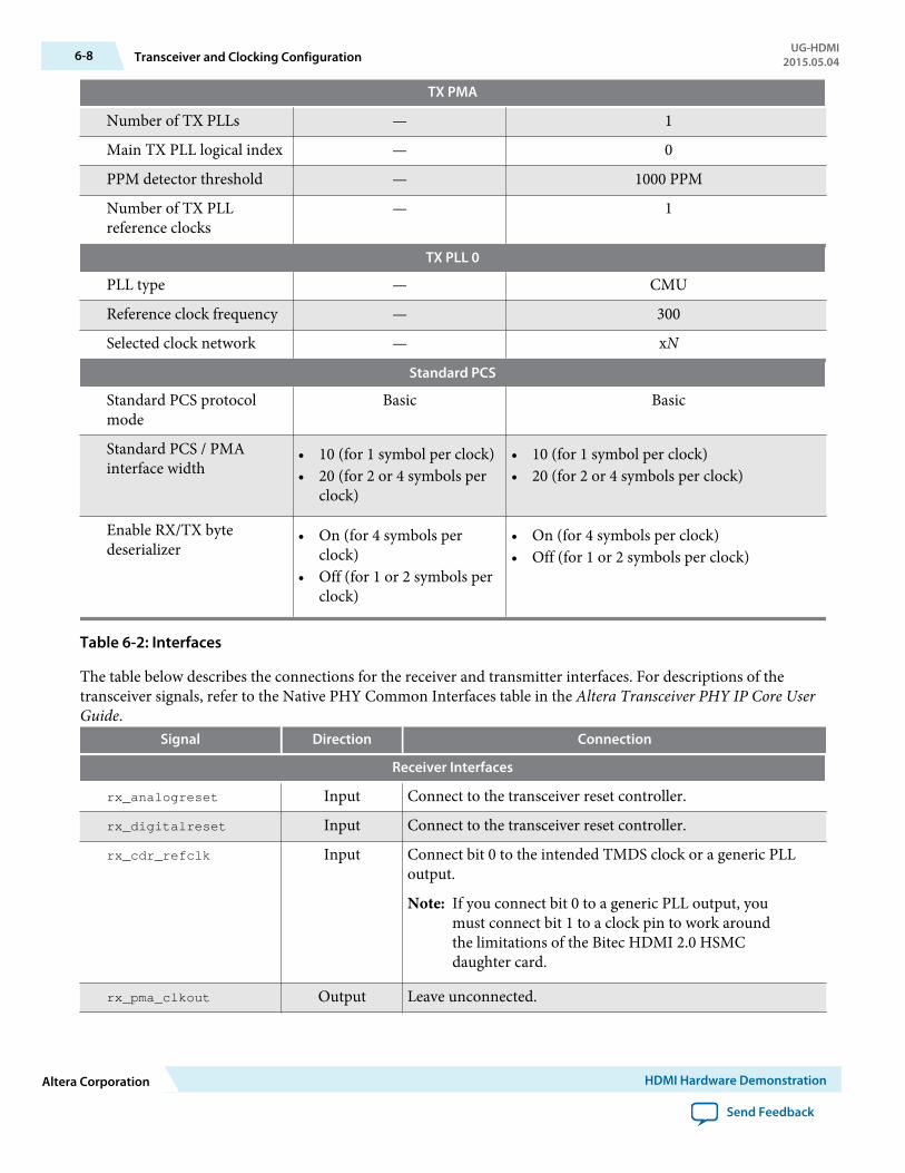
TX PMA
Number of TX PLLs — 1
Main TX PLL logical index — 0
PPM detector threshold — 1000 PPM
Number of TX PLLreference clocks
— 1
TX PLL 0
PLL type — CMU
Reference clock frequency — 300
Selected clock network — xN
Standard PCS
Standard PCS protocolmode
Basic Basic
Standard PCS / PMAinterface width
• 10 (for 1 symbol per clock)• 20 (for 2 or 4 symbols per
clock)
• 10 (for 1 symbol per clock)• 20 (for 2 or 4 symbols per clock)
Enable RX/TX bytedeserializer
• On (for 4 symbols perclock)
• Off (for 1 or 2 symbols perclock)
• On (for 4 symbols per clock)• Off (for 1 or 2 symbols per clock)
Table 6-2: Interfaces
The table below describes the connections for the receiver and transmitter interfaces. For descriptions of thetransceiver signals, refer to the Native PHY Common Interfaces table in the Altera Transceiver PHY IP Core UserGuide.
Signal Direction Connection
Receiver Interfaces
rx_analogreset Input Connect to the transceiver reset controller.
rx_digitalreset Input Connect to the transceiver reset controller.
rx_cdr_refclk Input Connect bit 0 to the intended TMDS clock or a generic PLLoutput.
Note: If you connect bit 0 to a generic PLL output, youmust connect bit 1 to a clock pin to work aroundthe limitations of the Bitec HDMI 2.0 HSMCdaughter card.
rx_pma_clkout Output Leave unconnected.
6-8 Transceiver and Clocking ConfigurationUG-HDMI
2015.05.04
Altera Corporation HDMI Hardware Demonstration
Send Feedback
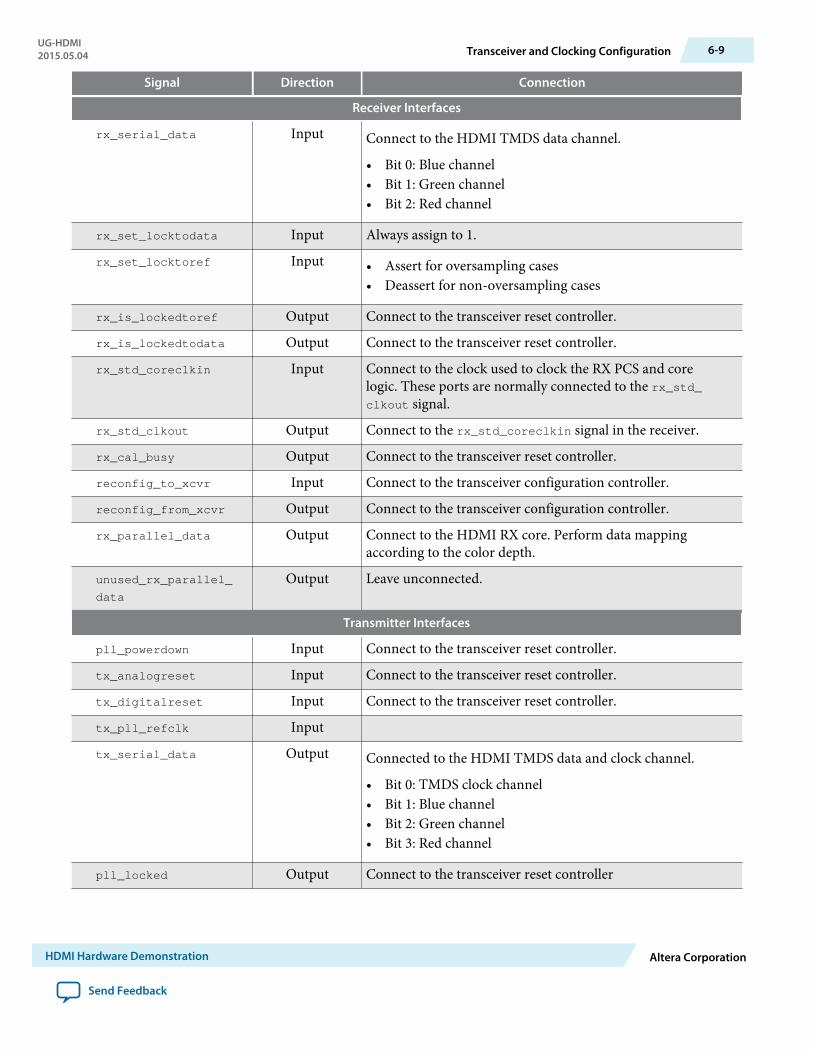
Signal Direction Connection
Receiver Interfaces
rx_serial_data Input Connect to the HDMI TMDS data channel.
• Bit 0: Blue channel• Bit 1: Green channel• Bit 2: Red channel
rx_set_locktodata Input Always assign to 1.
rx_set_locktoref Input • Assert for oversampling cases• Deassert for non-oversampling cases
rx_is_lockedtoref Output Connect to the transceiver reset controller.
rx_is_lockedtodata Output Connect to the transceiver reset controller.
rx_std_coreclkin Input Connect to the clock used to clock the RX PCS and corelogic. These ports are normally connected to the rx_std_clkout signal.
rx_std_clkout Output Connect to the rx_std_coreclkin signal in the receiver.
rx_cal_busy Output Connect to the transceiver reset controller.
reconfig_to_xcvr Input Connect to the transceiver configuration controller.
reconfig_from_xcvr Output Connect to the transceiver configuration controller.
rx_parallel_data Output Connect to the HDMI RX core. Perform data mappingaccording to the color depth.
unused_rx_parallel_
data
Output Leave unconnected.
Transmitter Interfaces
pll_powerdown Input Connect to the transceiver reset controller.
tx_analogreset Input Connect to the transceiver reset controller.
tx_digitalreset Input Connect to the transceiver reset controller.
tx_pll_refclk Input
tx_serial_data Output Connected to the HDMI TMDS data and clock channel.
• Bit 0: TMDS clock channel• Bit 1: Blue channel• Bit 2: Green channel• Bit 3: Red channel
pll_locked Output Connect to the transceiver reset controller
UG-HDMI2015.05.04 Transceiver and Clocking Configuration 6-9
HDMI Hardware Demonstration Altera Corporation
Send Feedback
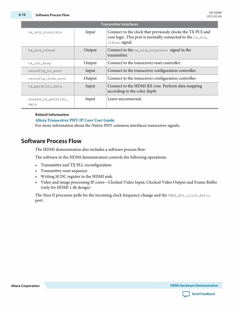
Transmitter Interfaces
tx_std_coreclkin Input Connect to the clock that previously clocks the TX PCS andcore logic. This port is normally connected to the rx_std_clkout signal.
tx_std_clkout Output Connect to the tx_std_coreclkin signal in thetransmitter.
tx_cal_busy Output Connect to the transceiver reset controller.
reconfig_to_xcvr Input Connect to the transceiver configuration controller.
reconfig_from_xcvr Output Connect to the transceiver configuration controller.
tx_parallel_data Input Connect to the HDMI RX core. Perform data mappingaccording to the color depth
unused_tx_parallel_
data
Input Leave unconnected.
Related InformationAltera Transceiver PHY IP Core User GuideFor more information about the Native PHY common interfaces transceiver signals.
Software Process FlowThe HDMI demonstration also includes a software process flow.
The software in the HDMI demonstration controls the following operations:
• Transmitter and TX PLL reconfiguration• Transmitter reset sequence• Writing SCDC register in the HDMI sink.• Video and image processing IP cores—Clocked Video Input, Clocked Video Output and Frame Buffer
(only for HDMI 1.4b design)
The Nios II processor polls for the incoming clock frequency change and the TMDS_Bit_clock_Ratioport.
6-10 Software Process FlowUG-HDMI
2015.05.04
Altera Corporation HDMI Hardware Demonstration
Send Feedback
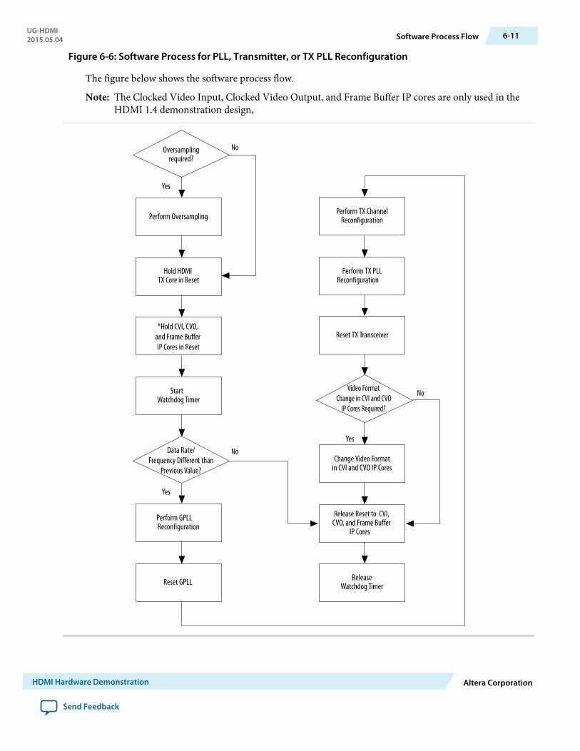
Figure 6-6: Software Process for PLL, Transmitter, or TX PLL Reconfiguration
The figure below shows the software process flow.
Note: The Clocked Video Input, Clocked Video Output, and Frame Buffer IP cores are only used in theHDMI 1.4 demonstration design,
Hold HDMI TX Core in Reset
Oversamplingrequired?
No
Yes
Perform Oversampling
*Hold CVI, CVO, and Frame Buffer IP Cores in Reset
Start Watchdog Timer
Perform GPLL Reconfiguration
Reset GPLL
Data Rate/Frequency Different than
Previous Value?
No
Yes
Perform TX ChannelReconfiguration
Perform TX PLLReconfiguration
Reset TX Transceiver
Change Video Formatin CVI and CVO IP Cores
Yes
No
Release Reset to CVI, CVO, and Frame Buffer
IP Cores
ReleaseWatchdog Timer
Video Format Change in CVI and CVO
IP Cores Required?
UG-HDMI2015.05.04 Software Process Flow 6-11
HDMI Hardware Demonstration Altera Corporation
Send Feedback
Demonstration WalkthroughSetting up and running the HDMI hardware demonstration consists of four stages.
You can use the Altera-provided scripts to automate these stages.
1. Set up the hardware.2. Copy the design files to your working directory.3. Build and download the design.4. Power up the HDMI monitor and view the results.
Set Up the HardwareThe first stage of the demonstration is to set up the hardware.
To set up the hardware for the demonstration:
1. Connect the Bitec daughter card to the Arria V GX starter board or Stratix V GX FPGA developmentboard.
2. Connect the board to your PC using a USB cable.
Note: The Arria V GX FPGA starter board and the Stratix V GX FPGA development board have anOn-Board USB-Blaster™ II connection. If your version of the board does not have thisconnection, you can use an external USB-Blaster cable.
3. Connect an HDMI cable from the HDMI RX on the Bitec HSMC daughter card, and leave the otherend unconnected.
4. Connect another HDMI cable from the HDMI TX on the Bitec HSMC daughter card to a HDMImonitor.
Copy the Design FilesAfter you set up the hardware, you copy the design files.Copy the hardware demonstration files from one of the following paths to your working directory:
• Arria V
• HDMI 1.4 demonstration: <IP root directory>/altera/altera_hdmi/hw_demo/av_sk
• HDMI 2.0 demonstration: <IP root directory>/altera/altera_hdmi/hw_demo/av_sk_hdmi2
• Stratix V
• HDMI 1.4 demonstration: <IP root directory>/altera/altera_hdmi/hw_demo/sv
• HDMI 2.0 demonstration: <IP root directory>/altera/altera_hdmi/hw_demo/sv_hdmi2
Build the DesignAfter you copy the design files, you can build the design.
You can use a Tcl script to build and compile the FPGA design.
1. Open a Nios II Command Shell.2. Change the directory to your working directory.3. Type the command and enter.
source runall.tcl
6-12 Demonstration WalkthroughUG-HDMI
2015.05.04
Altera Corporation HDMI Hardware Demonstration
Send Feedback

This script executes the following commands:
• Generate IP catalog files• Generate the Qsys system• Create a Quartus II project• Create a software work space and build it• Compile the Quartus II project• Run Analysis & Synthesis to generate a post-map netlist for DDR assignments• Perform a full compile
Note: If you are a Linux user, you will get a message cygpath: command not found. You can safelyignore this message; the script will proceed to generate the next commands.
View the ResultsAt the end of the demonstration, you will be able to view the results on the HDMI monitor.
To view the results of the demonstration, follow these steps:
1. Power up the development board.2. Type the following command to download the Software Object File (.sof) to the FPGA.
nios2-configure-sof hdmi_demo_example_av.sof (Arria V GX)
or
nios2-configure-sof hdmi_demo_example_sv.sof (Stratix V GX)3. Connect the unconnected end of the HDMI cable to a video source.4. Power up the HDMI monitor (if you haven't done so).
The design displays the output of your video source (PC).5. Open the graphic card control utility (if you are using a PC as source).
You will see the words BITEC_HDMI_4K on the screen. Using the control panel, you can switch betweenthe various video resolutions. This demonstration allows 640×480p60, 720×480p60, 1280×720p60,1920×1080p60, 3840×2160p24, and 3840×2160p60 (for HDMI 2.0 design only).
Guidelines
• If you do not see visible output on the monitor, try unplugging the cable from your source and plug itback again (hot-plug detection). Make sure that USER_LED0, USER_LED1 and USER_LED2 on the boardare illuminated; indicating HDMI RX core has locked correctly.
• Pressing CPU_RST triggers reset to the whole design while USER_LED3 and USER_LED7 are indicatingoversampling mode is enabled in RX and TX HDMI core respectively.
• USER_LED4, USER_LED5, and USER_LED6 are indicating the status of DDR3 in the design.
• USER_LED4 indicates DDR3 initialization has completed• USER_LED5 indicates DDR3 calibration is successful• USER_LED6 indicates DDR3 calibration has failed
If you see USER_LED6 illuminating, in the Nios II command shell, type cpu_reset to reset the system.
UG-HDMI2015.05.04 View the Results 6-13
HDMI Hardware Demonstration Altera Corporation
Send Feedback
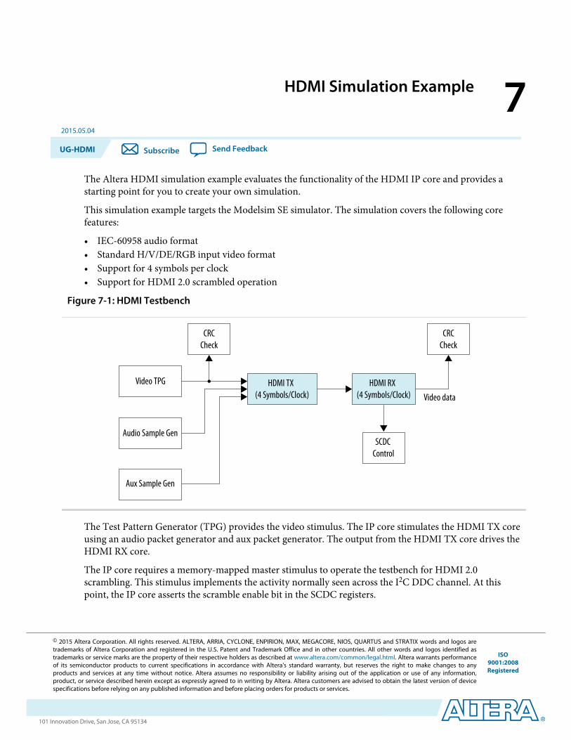
HDMI Simulation Example 72015.05.04
UG-HDMI Subscribe Send Feedback
The Altera HDMI simulation example evaluates the functionality of the HDMI IP core and provides astarting point for you to create your own simulation.
This simulation example targets the Modelsim SE simulator. The simulation covers the following corefeatures:
• IEC-60958 audio format• Standard H/V/DE/RGB input video format• Support for 4 symbols per clock• Support for HDMI 2.0 scrambled operation
Figure 7-1: HDMI Testbench
HDMI TX(4 Symbols/Clock)
HDMI RX(4 Symbols/Clock)
CRCCheck
Video TPG
CRCCheck
Video data
SCDC Control
Audio Sample Gen
Aux Sample Gen
The Test Pattern Generator (TPG) provides the video stimulus. The IP core stimulates the HDMI TX coreusing an audio packet generator and aux packet generator. The output from the HDMI TX core drives theHDMI RX core.
The IP core requires a memory-mapped master stimulus to operate the testbench for HDMI 2.0scrambling. This stimulus implements the activity normally seen across the I2C DDC channel. At thispoint, the IP core asserts the scramble enable bit in the SCDC registers.
© 2015 Altera Corporation. All rights reserved. ALTERA, ARRIA, CYCLONE, ENPIRION, MAX, MEGACORE, NIOS, QUARTUS and STRATIX words and logos aretrademarks of Altera Corporation and registered in the U.S. Patent and Trademark Office and in other countries. All other words and logos identified astrademarks or service marks are the property of their respective holders as described at www.altera.com/common/legal.html. Altera warrants performanceof its semiconductor products to current specifications in accordance with Altera's standard warranty, but reserves the right to make changes to anyproducts and services at any time without notice. Altera assumes no responsibility or liability arising out of the application or use of any information,product, or service described herein except as expressly agreed to in writing by Altera. Altera customers are advised to obtain the latest version of devicespecifications before relying on any published information and before placing orders for products or services.
ISO9001:2008Registered
www.altera.com101 Innovation Drive, San Jose, CA 95134
The testbench implements CRC checking on the input and output video. The testbench checks the CRCvalue of the transmitted data against the CRC calculated in the received video data. The testbenchperforms the checking after detecting 4 stable V-SYNC signals from the receiver.
Simulation WalkthroughSetting up and running the HDMI simulation example consists of two steps.
1. Copy the simulation files from <IP root directory>/altera/altera_hdmi/sim_example to your workingdirectory.
2. Generate the IP simulation files and scripts, compile, and simulate.a. Open your command prompt.b. Type the command below and enter.
sh runall.sh
This script executes the following commands:
7-2 Simulation WalkthroughUG-HDMI
2015.05.04
Altera Corporation HDMI Simulation Example
Send Feedback

Command
Generate the simulation files for theHDMI cores.
• ip-generate --project-directory=./ --component-
file=./hdmi_rx_single.qsys --output-directory=./
hdmi_rx_single/sim/ --file-set=SIM_VERILOG --
report-file=sopcinfo:./hdmi_rx_single.sopcinfo -
-report-file=html:./hdmi_rx_single.html --
report-file=spd:./hdmi_rx_single/sim/hdmi_rx_
single.spd --report-file=qip:./hdmi_rx_single/
sim/hdmi_rx_single.qip
• ip-generate --project-directory=./ --component-
file=./hdmi_rx_double.qsys --output-directory=./
hdmi_rx_double/sim/ --file-set=SIM_VERILOG --
report-file=sopcinfo:./hdmi_rx_double.sopcinfo -
-report-file=html:./hdmi_rx_double.html --
report-file=spd:./hdmi_rx_double/sim/hdmi_rx_
double.spd --report-file=qip:./hdmi_rx_double/
sim/hdmi_rx_double.qip
• ip-generate --project-directory=./ --component-
file=./hdmi_tx_single.qsys --output-directory=./
hdmi_tx_single/sim/ --file-set=SIM_VERILOG --
report-file=sopcinfo:./hdmi_tx_single.sopcinfo -
-report-file=html:./hdmi_tx_single.html --
report-file=spd:./hdmi_tx_single/sim/hdmi_tx_
single.spd --report-file=qip:./hdmi_tx_single/
sim/hdmi_tx_single.qip
• ip-generate --project-directory=./ --component-
file=./hdmi_tx_double.qsys --output-directory=./
hdmi_tx_double/sim/ --file-set=SIM_VERILOG --
report-file=sopcinfo:./hdmi_tx_double.sopcinfo -
-report-file=html:./hdmi_tx_double.html --
report-file=spd:./hdmi_tx_double/sim/hdmi_tx_
double.spd --report-file=qip:./hdmi_tx_double/
sim/hdmi_tx_double.qip
Merge the four resulting msim_setup.tclscripts to create a single mentor/msim_setup.tcl script.
ip-make-simscript --spd=./hdmi_tx_single/sim/hdmi_
tx_single.spd --spd=./hdmi_tx_double/sim/hdmi_tx_
double.spd --spd=./hdmi_rx_single/sim/hdmi_rx_
single.spd --spd=./hdmi_rx_double/sim/hdmi_rx_
double.spd
Compile and simulate the design in theModelSim software.
vsim -c -do msim_hdmi.tcl
Generate the simulation files for theHDMI cores.
Merge the resulting msim_setup.tcl scriptsto create a single mentor/msim_setup.tclscript.
UG-HDMI2015.05.04 Simulation Walkthrough 7-3
HDMI Simulation Example Altera Corporation
Send Feedback
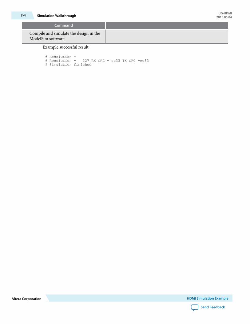
Command
Compile and simulate the design in theModelSim software.
Example successful result:
# Resolution = # Resolution = 127 RX CRC = ee33 TX CRC =ee33 # Simulation finished
7-4 Simulation WalkthroughUG-HDMI
2015.05.04
Altera Corporation HDMI Simulation Example
Send Feedback
Additional Information for High-DefinitionMultimedia Interface User Guide A
2015.05.04
UG-HDMI Subscribe Send Feedback
Document Revision History for HDMI User GuideDate Version Changes
May 2015 2015.05.04 • Updated the HDMI IP core resource utilization table with 15.0information.
• Added information about 4 symbols per clock mode.• Added information about Status and Control Data Channel (SCDC)
for HDMI specification version 2.0.• Added the following interface ports for HDMI source:
• TMDS_Bit_clock_Ratio
• Scrambler_Enable
• Added the TMDS_Bit_clock_Ratio interface port for HDMI sink.• Updated the HDMI hardware demonstration design with HDMI 2.0
information.• Added software process flow for the HDMI hardware demonstration.
December2014
2014.12.15 Initial release.
© 2015 Altera Corporation. All rights reserved. ALTERA, ARRIA, CYCLONE, ENPIRION, MAX, MEGACORE, NIOS, QUARTUS and STRATIX words and logos aretrademarks of Altera Corporation and registered in the U.S. Patent and Trademark Office and in other countries. All other words and logos identified astrademarks or service marks are the property of their respective holders as described at www.altera.com/common/legal.html. Altera warrants performanceof its semiconductor products to current specifications in accordance with Altera's standard warranty, but reserves the right to make changes to anyproducts and services at any time without notice. Altera assumes no responsibility or liability arising out of the application or use of any information,product, or service described herein except as expressly agreed to in writing by Altera. Altera customers are advised to obtain the latest version of devicespecifications before relying on any published information and before placing orders for products or services.
ISO9001:2008Registered
www.altera.com101 Innovation Drive, San Jose, CA 95134


