222
AM–500A 500 WATT AM–1A 1 KILOWATT AM BROADCAST TRANSMITTERS October, 1999 IM No. 597–1112

AM–500A 500 WATTAM–1A 1 KILOWATTAM BROADCASTTRANSMITTERS
October, 1999 IM No. 597–1112

IMPORTANT INFORMATION
EQUIPMENT LOST OR DAMAGED IN TRANSIT.When delivering the equipment to you, the truck driver or carrier’s agent will present a receipt for your signature.Do not sign it until you have: 1) inspected the containers for visible signs of damage and 2) counted the containersand compared with the amount shown on the shipping papers. If a shortage or evidence of damage is noted, insistthat notation to that effect be made on the shipping papers before you sign them.
Further, after receiving the equipment, unpack it and inspect thoroughly for concealed damage. If concealed dam-age is discovered, immediately notify the carrier, confirming the notification in writing, and secure an inspection re-port. This item should be unpacked and inspected for damage WITHIN 15 DAYS after receipt. Claims for loss ordamage will not be honored without proper notification of inspection by the carrier.
RF PRODUCT TECHNICAL ASSISTANCE – REPAIR SERVICE – REPLACEMENT PARTS.
Technical assistance is available from Broadcast Electronics by letter, prepaid telephone, fax, or E–mail. Equip-ment requiring repair or overhaul should be sent by common carrier, prepaid, insured, and well protected. If propershipping materials are not available, contact the Customer Service Department for a shipping container. Do not themail equipment. We can assume no liability for inbound damage, and necessary repairs become the obligation ofthe shipper. Prior arrangement is necessary. Contact the Customer Service Department for a Return Authoriza-tion.
Emergency and warranty replacement parts may be ordered from the following address. Be sure to include theequipment model number, serial number, part description, and part number. Non–emergency replacement partsmay be ordered directly from the Broadcast Electronics stock room by fax at the number shown below.
FACILITY CONTACTS –
Broadcast Electronics, Inc. – Quincy Facility4100 N. 24th St. P.O. BOX 3606Quincy, Illinois 62305Telephone: (217) 224–9600Fax: (217) 224–9607E–Mail: General – [email protected] Site: www.bdcast.com
RF PRODUCT TECHNICAL ASSISTANCE – REPAIR – EMERGENCY/WARRANTY REPLACEMENT PARTS –
Telephone: (217) 224–9600E–Mail: [email protected]: (217) 224–9607
NON–EMERGENCY REPLACEMENT PARTS –
Fax: (217) 224–9609
RETURN, REPAIR, AND EXCHANGES.
Do not return any merchandise without our written approval and Return Authorization. We will provide special ship-ping instructions and a code number that will assure proper handling and prompt issuance of credit. Please furnishcomplete details as to circumstances and reasons when requesting return of merchandise. All returned merchan-dise must be sent freight prepaid and properly insured by the customer.
WARRANTY ADJUSTMENT.
Broadcast Electronics, Inc. warranty is included in the Terms and Conditions of Sale. In the event of a warrantyclaim, replacement or repair parts will be supplied F.O.B. factory. At the discretion of Broadcast Electronics, thecustomer may be required to return the defective part or equipment to Broadcast Electronics, Inc. F.O.B. Quincy,Illinois. Warranty replacements of defective merchandise will be billed to your account. This billing will be clearedby a credit issued upon return of the defective item.
PROPRIETARY NOTICE.
This document contains proprietary data of Broadcast Electronics, Inc. No disclosure, reproduction, or use of anypart thereof may be made except by prior written permission.
MODIFICATIONS.
Broadcast Electronics, Inc. reserves the right to modify the design and specifications of the equipment in this manu-al without notice. Any modifications shall not adversely affect performance of the equipment so modified.
WARNING
OPERATING HAZARDS
READ THIS SHEET AND OBSERVE ALL SAFETY PRECAUTIONS
ALL PERSONS WHO WORK WITH OR ARE EXPOSED TO POWER TRANSISTORS MUST TAKE PRECAUTIONSTO PROTECT THEMSELVES AGAINST POSSIBLE SERIOUS BODILY INJURY. EXERCISE EXTREME CAREAROUND SUCH PRODUCTS. UNINFORMED OR CARELESS OPERATION OF THESE DEVICES CAN RESULTIN POOR PERFORMANCE, DAMAGE TO THE DEVICE OR PROPERTY, SERIOUS BODILY INJURY, AND POSSI-BLY DEATH.
DANGEROUS HAZARDS EXIST IN THE OPERATION OF POWER TRANSISTORS
The operation of power tubes and power transistors involves one or more of the following hazards, any one of which,in the absence of safe operating practices and precautions, could result in serious harm to personnel.
A. HIGH VOLTAGE – Normal operating voltages can be deadly. Additional information follows.
B. RF RADIATION – Exposure to RF radiation may cause serious bodily injury possibly resulting in blindness or death. Cardiac pacemakers may be affected. Additional information follows.
C. BERYLLIUM – OXIDE POISONING – Dust or fumes from BeO ceramics used as thermal links with power transistors are highly toxic and can cause serious injury or death. Additional information follows.
D. HOT SURFACES – Surfaces of air–cooled heat sinks radiators can reach temperatures of 100 degrees centigrade and cause burns if touched. Additional information follows.
E. RF BURNS – Circuit boards with RF power transistors contain high RF potentials. Do not operate an RF power module with the cover removed.
HIGH VOLTAGE
The transmitter operates at voltages high enough to kill through electrocution. Personnel should always break theprimary circuits when access to the transmitter is required.
RADIO FREQUENCY RADIATION
Exposure of personnel to RF radiation should be minimized, personnel should not be permitted in the vicinity of openenergized RF generating circuits, or RF transmission systems (waveguides, cables, connectors, etc.), or energizedantennas. It is generally accepted that exposure to “high levels” of radiation can result in severe bodily injury includ-ing blindness. Cardiac pacemakers may be affected.
The effect of prolonged exposure to “low level” RF radiation continues to be a subject of investigation and controver-sy. It is generally agreed that prolonged exposure of personnel to RF radiation should be limited to an absolute mini-mum. It is also generally agreed that exposure should be reduced in working areas where personnel heat load isabove normal. A 10 mW/cm2 per one tenth hour average level has been adopted by several U.S. Government agen-cies including the Occupational Safety and Health Administration (OSHA) as the standard protection guide for em-ployee work environments. An even stricter standard is recommended by the American National Standards Institutewhich recommends a 1.0 mW/cm2 per one tenth hour average level exposure between 30 Hz and 300 MHz as thestandard employee protection guide (ANSI C95.1–1982).
RF energy must be contained properly by shielding and transmission lines. All input and output RF connections, suchas cables, flanges and gaskets must be RF leakproof. Never operate a power tube without a properly matched RFenergy absorbing load attached. Never look into or expose any part of the body to an antenna, open RF generatingcircuit, or RF transmission system while energized. Monitor the tube and RF system for RF radiation leakage at regu-lar intervals and after servicing.
DANGER –– BERYLLIUM OXIDE CERAMICS (BeO) – AVOID BREATHING DUST OR FUMES
BeO ceramic material is used as a thermal link to carry heat from a transistor to the heat sink. Do not perform anyoperation on any BeO ceramic which might produce dust or fumes, such as grinding, grit blasting, or acid cleaning.Beryllium oxide dust or fumes are highly toxic and breathing them can result in serious personal injury or death. BeOceramics must be disposed of only in a manner prescribed by the device manufacturer.
HOT SURFACES
Heat sinks and reject loads are air–cooled or conduction–cooled. The air–cooled external surface can operate at ahigh temperature (up to 100° C). All hot surfaces may remain hot for an extended time after the transmitter is oper-ated to off. To prevent serious burns, take care to prevent and avoid any bodily contact with these surfaces both dur-ing and for a reasonable cooling down period after operation.
TRANSMITTER WARRANTY VOID NOTICE
THE PRODUCT WARRANTY WILL BE VOID IF THE
TRANSMITTER IS INSTALLED AT A SITE WITH
INADEQUATE LIGHTNING PROTECTION AND A
DEFECTIVE TRANSMISSION LINE SYSTEM.
The transmitter is covered by a two year limited product warranty from Broadcast Elec�
tronics. However, the transmitter must be properly installed at a site with adequate
lightning protection and transmission line systems. TO ENSURE THE TRANSMIT�
TER WARRANTY IS VALID, the transmitter must be installed: 1) as described by the
INSTALLATION procedures presented in SECTION II of this manual, 2) at a transmitter
site with a lightning protection system described in TRANSMITTER SITE LIGHTNING
PROTECTION SYSTEM CHECKOUT (refer to SECTION II of this manual), and 3) at a
transmitter site with a transmission line system described in TRANSMISSION LINE
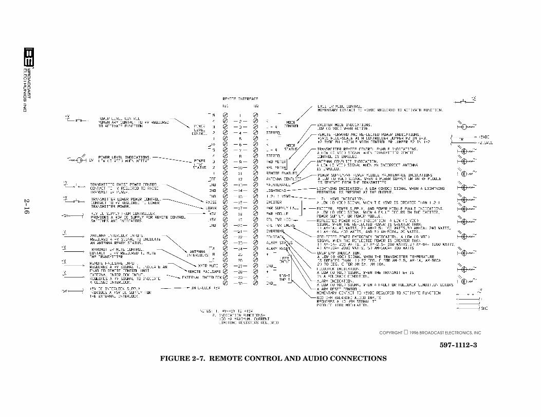
AND ANTENNA CHECKOUT (refer to SECTION II of this manual). FAILURE TO
PROPERLY INSTALL THE TRANSMITTER, PROVIDE AN ADEQUATE LIGHT�
NING PROTECTION SYSTEM, OR PROVIDE AN ADEQUATE TRANSMISSION
LINE SYSTEM WILL VOID THE WARRANTY ON THE TRANSMITTER. If any
questions develop concerning the transmitter warranty and installation site systems, con�
tact the Broadcast Electronics Customer Service Department.
BROADCAST ELECTRONICS, INC.

NOTICE TO THE EQUIPMENT USER
FCC Rule 73.1590 mandates the licensee of each AM station to make measurements forspurious and harmonic emissions to show compliance with the transmission system re�quirements of Section 73.44 of the Commission's Rules. It is the broadcast station's respon�sibility to ensure that the audio signal input to the Broadcast Electronics A-Series trans�
mitters conforms to the audio standard NRSC-1 (published as ANSI/EIA-549-1988). Thisis a mandatory requirement to ensure that the equipment complies to Section 73.44 andSection 73.128(C) of the Commission's Rules.
BROADCAST ELECTRONICS, INC.

WARNING WARNING
OPERATING HAZARDS
WARNING
WARNING
THE TRANSMITTER CONTAINS MULTIPLE CIRCUIT
GROUNDS WITH HIGH AC AND DC POTENTIALS WITH
RESPECT TO THE CABINET WHICH IS AT EARTH PO�
TENTIAL. DO NOT ENERGIZE THE TRANSMITTER
WITH TEST EQUIPMENT CONNECTED TO THE
TRANSMITTER OUTPUT NETWORK, RF POWER MOD�
ULE, RF COMBINER, OR POWER SUPPLY COMPO�
NENTS.
The Broadcast Electronics AM transmitters contain high voltages and currents. If safety precautions are
not practiced, contact with the high voltages and currents could cause serious injury or death. The trans�
mitter is equipped with many built-in safety features, however good judgement, care, and common sense
must be practiced to prevent accidents.
In addition to high voltages and currents, the AM transmitters contain multiple circuit grounds with
high ac and dc potentials with respect to the cabinet which is at earth potential. The potentials could
cause serious injury or death if maintenance personnel simultaneously touch a circuit ground and the
cabinet. As a result, operation of the transmitter with test equipment connected to transmitter output
network, RF power module, RF combiner, or power supply components is extremely dangerous and must
not be attempted. Therefore, never energize the transmitter with test equipment connected to the trans�
mitter output network, RF power module, RF combiner, or power supply components. Test equipment
may be connected to the ECU circuit boards from the front of the transmitter using the supplied extender
circuit board with power energized if required.
i
Broadcast Electronics 1996 ALL RIGHTS RESERVED Printed in the U.S.A.
TABLE OF CONTENTS
PARAGRAPH PAGE NO.
SECTION I GENERAL INFORMATION
1-1 INTRODUCTION 1-1
1-3 EQUIPMENT DESCRIPTION 1-1
1-4 GENERAL 1-1
1-6 EXCITER/CONTROL UNIT 1-1
1-12 OUTPUT NETWORK CHASSIS 1-3
1-16 TRANSMITTER CONFIGURATIONS 1-3
1-18 ACCESSORIES AND SPARE PARTS KITS 1-3
1-20 EQUIPMENT SPECIFICATIONS 1-3
SECTION II INSTALLATION
2-1 INTRODUCTION 2-1
2-3 UNPACKING 2-1
2-6 ENVIRONMENTAL REQUIREMENTS 2-1
2-8 INSTALLATION 2-1
2-10 EQUIPMENT PLACEMENT 2-1
2-12 RACK PREPARATION 2-1
2-14 EQUIPMENT INSTALLATION 2-2
2-15 TRANSMITTER MOUNTING 2-2
2-19 COMPONENT INSTALLATION 2-8
2-22 ECU CIRCUIT BOARDS 2-8
2-23 RF POWER MODULE 2-8
2-24 BATTERY INSTALLATION 2-8
2-25 CIRCUIT BOARD PROGRAMMING 2-8
2-27 EXCITER CIRCUIT BOARD 2-10
2-36 STEREO CIRCUIT BOARD 2-10
2-41 CONTROLLER CIRCUIT BOARD 2-13
2-54 POWER SUPPLY CIRCUIT BOARD 2-15
2-57 REMOTE CONTROL CONNECTIONS 2-15
2-58 GENERAL 2-15
2-83 WIRING 2-18
2-85 AUDIO INPUT CONNECTION 2-18
2-87 EXTERNAL STEREO RF INPUT 2-19
2-88 RF TRANSMISSION LINE CONNECTION 2-19
2-89 EXTERNAL INTERLOCK 2-19
2-90 MODULATION MONITOR 2-20
2-91 AC POWER CONNECTIONS 2-20
2-94 GROUND 2-20
2-95 TRANSMITTER SITE LIGHTNING PROTECTION 2-22SYSTEM CHECKOUT
2-97 ANTENNA BALL-GAP LIGHTNING 2-22ARRESTOR
2-101 ANTENNA-TUNING-UNIT SPARK-GAP 2-22LIGHTNING ARRESTOR
2-102 TRANSMITTER SITE GROUNDING SYSTEM 2-24
2-103 CABLE PROTECTION 2-24
2-110 ANTENNA RF FEED LINE 2-24
ii
PARAGRAPH PAGE NO.
2-111 TRANSMISSION LINE AND ANTENNA 2-25CHECKOUT
2-113 ANTENNA VSWR 2-25
2-114 COAXIAL SWITCH CONTROLLER. 2-25
2-115 ATU AND PHASOR CHECKOUT 2-25
2-116 INITIAL CHECKOUT 2-25
2-118 PRELIMINARY OPERATION AND ADJUSTMENT 2-26
2-123 POWER LEVEL AND MODULATION MONITOR 2-26CALIBRATION ADJUSTMENTS
2-135 STEREO ADJUSTMENT 2-28
2-146 SINGLE CHANNEL LEVEL 2-30
SECTION III OPERATION
3-1 INTRODUCTION 3-1
3-3 CONTROLS AND INDICATORS 3-1
3-5 OPERATION 3-12
3-6 TURN-ON 3-12
3-7 OPERATION 3-12
3-14 TURN OFF 3-12
3-16 METERING 3-13
3-17 FORWARD POWER 3-13
3-18 REFLECTED POWER 3-13
3-19 POWER ADJUST 3-13
3-21 MONO/STEREO OPERATION 3-13
3-23 STEREO OPERATION 3-13
3-24 MONO OPERATION 3-13
3-27 PILOT CONTROL 3-14
3-29 EXCITER MONITOR OPERATION 3-14
3-31 MONO/STEREO INDICATIONS 3-14
3-32 INPUT SELECTION 3-14
3-33 POLARITY SELECTION 3-14
3-34 X10 AUTORANGE INDICATIONS 3-14
3-35 FAULT RESET 3-15
3-37 POWER SUPPLY FAULT RESET 3-15
3-39 OVER-CYCLE OFF 3-15
3-41 OVER-MODULATION PWM MUTE 3-15
3-43 TRANSMITTER MONITOR 3-15
3-45 BATTERY TEST 3-15
3-47 CONTROLLER PWM MUTE INDICATOR 3-15
3-49 CONTROLLER REMOTE FAIL�SAFE 3-16INDICATOR.
3-51 EXCITER LOCK INDICATOR 3-16
3-53 EXCITER +5V/+15V/-15V INDICATORS 3-16
3-55 STEREO EQUALIZATION INDICATORS 3-16
3-57 RF POWER MODULE INDICATORS 3-16
3-59 HIGH AC LINE CONDITIONS 3-16
SECTION IV THEORY OF OPERATION
4-1 INTRODUCTION 4-1
4-3 OVERALL OPERATION 4-1

iii
PARAGRAPH PAGE NO.
4-5 POWER SUPPLY CIRCUITRY OPERATION 4-1
4-7 POWER SUPPLY CIRCUIT BOARD OPERATION 4-1
4-9 RF CIRCUITRY OPERATION 4-1
4-11 RF POWER MODULE MODULATOR CIRCUIT 4-1BOARD OPERATION
4-13 RF POWER MODULE AMPLIFIER CIRCUIT 4-1BOARD OPERATION
4-15 CONTROLLER CIRCUIT BOARD OPERATION 4-1
4-17 EXCITER CIRCUIT BOARD OPERATION 4-1
4-19 STEREO CIRCUIT BOARD OPERATION 4-1
SECTION V MAINTENANCE
5-1 INTRODUCTION 5-1
5-3 SAFETY CONSIDERATIONS 5-1
5-7 FIRST LEVEL MAINTENANCE 5-1
5-9 ROUTINE MAINTENANCE 5-2
5-10 INSPECTION AND CLEANING 5-2
5-11 CONTROLLER BATTERY 5-2
5-12 AIR FILTER 5-2
5-13 FLUSHING FAN 5-2
5-15 SPARK GAP 5-2
5-16 SECOND LEVEL MAINTENANCE 5-2
5-19 OVERALL TRANSMITTER 5-3
5-20 ELECTRICAL ADJUSTMENTS 5-3
5-21 TRANSMITTER FREQUENCY 5-3RE-PROGRAMMING
5-23 TROUBLESHOOTING 5-3
5-25 TRANSMITTER INDICATORS 5-4
5-26 TRANSMITTER TROUBLESHOOTING 5-6PROCEDURES
5-27 TRANSMITTER COMPONENT LOCATIONS 5-6
5-28 POWER SUPPLY CIRCUIT BOARD 5-11
5-29 SAFETY CONSIDERATIONS 5-11
5-31 REMOVING/INSTALLING A POWER SUPPLY 5-11CIRCUIT BOARD
5-35 TROUBLESHOOTING PROCEDURES 5-11
5-37 RF POWER MODULE 5-17
5-38 SAFETY CONSIDERATIONS 5-17
5-40 RF POWER MODULE ASSEMBLY PROCEDURE 5-17
5-42 RF POWER MODULE EXCHANGE PROGRAM 5-18
5-44 TROUBLESHOOTING PROCEDURES 5-18
5-46 DIRECTIONAL COUPLER/LIGHTNING 5-20DETECTION/LIGHTNING PROTECTION CIRCUIT BOARDS
5-47 SAFETY CONSIDERATIONS 5-20
5-49 ELECTRICAL ADJUSTMENTS 5-21
5-50 MODULATION CALIBRATION CONTROLS 5-21
5-51 DIRECTIONAL COUPLER NULL CONTROLS 5-21
5-52 TROUBLESHOOTING PROCEDURES 5-21
5-55 ECU 5-22

iv
PARAGRAPH PAGE NO.
5-56 SAFETY CONSIDERATIONS 5-22
5-58 ECU CIRCUIT BOARD INSTALLATION/REMOVAL 5-22
5-61 ELECTRICAL ADJUSTMENTS 5-23
5-63 ECU EXTENDER CIRCUIT BOARD OPERATION 5-23
5-65 CONTROLLER CIRCUIT BOARD ADJUSTMENTS 5-23
5-66 P1 SET - P5 SET CONTROLS 5-23
5-67 FWD AND RFL CALIBRATIONS 5-24
5-68 ECU METER SWITCH CIRCUIT BOARD 5-24ADJUSTMENTS
5-69 FORWARD POWER METER LOW AND HIGH 5-24SCALE CALIBRATIONS
5-70 REFLECTED POWER METER LOW AND HIGH 5-24SCALE CALIBRATIONS
5-71 FWD AND RFL CALIBRATIONS 5-24
5-72 STEREO CIRCUIT BOARD ADJUSTMENTS 5-24
5-73 STEREO ADJUSTMENT 5-24
5-74 EXCITER CIRCUIT BOARD ADJUSTMENTS 5-24
5-75 MODULATION CALIBRATION 5-24
5-76 PHASE MODULATOR CALIBRATION 5-24
5-77 SYMMETRY CONTROL 5-24
5-78 IPM CORRECTION CIRCUIT CONTROLS 5-25
5-79 SINGLE CHAN MONO LEVEL CONTROL 5-25
5-80 AVERAGE MODULATION LIMIT CONTROL 5-25
5-81 NEG LIMIT CONTROL 5-25
5-94 FREQUENCY CALIBRATION CONTROL 5-26
5-104 DISPLAY CIRCUIT BOARD ADJUSTMENTS 5-27
5-105 L/L+R AND R/L-R DISPLAY CALIBRATION 5-27CONTROL
5-117 TROUBLESHOOTING PROCEDURES 5-27
5-119 COMPONENT REPLACEMENT PROCEDURE 5-32
5-125 INTEGRATED CIRCUITS 5-33
SECTION VI PARTS LIST
6-1 INTRODUCTION 6-1
SECTION VII DRAWINGS
7-1 INTRODUCTION 7-1
SECTION A APPENDIX
Introduction A-1
LIST OF TABLES
TABLE NO. TITLE PAGE NO.
1-1 ELECTRICAL CHARACTERISTICS 1-4
1-2 PHYSICAL AND ENVIRONMENTAL 1-7CHARACTERISTICS
3-1 AM-1A/AM-500A CONTROLS AND INDICATORS 3-1
3-2 ECU CONTROLS AND INDICATORS 3-3
v
TABLE NO. TITLE PAGE NO.
3-3 POWER MODULE CONTROLS AND INDICATORS 3-10
5-1 AM-1A/AM-500A INDICATORS 5-4
5-2 AM-1A/AM-500A TROUBLESHOOTING 5-7
5-3 POWER SUPPLY MODULE TROUBLESHOOTING 5-16
5-4 RF POWER MODULE TROUBLESHOOTING 5-18
5-5 DIRECTIONAL COUPLER CIRCUIT BOARD 5-21TROUBLESHOOTING
5-6 LIGHTNING DETECTION CIRCUIT BOARD/SPARK GAP 5-22TROUBLESHOOTING
5-7 LIGHTNING PROTECTION CIRCUIT BOARD 5-22TROUBLESHOOTING
5-8 EXCITER CIRCUIT BOARD TROUBLESHOOTING 5-28
5-9 STEREO CIRCUIT BOARD TROUBLESHOOTING 5-30
5-10 CONTROLLER CIRCUIT BOARD TROUBLESHOOTING 5-31
5-11 ECU POWER SUPPLY TROUBLESHOOTING 5-32
6-1 AM-1A REPLACEABLE PARTS LIST INDEX 6-1
LIST OF ILLUSTRATIONS
FIGURE DESCRIPTION PAGE NO.
1-1 AM-1A TRANSMITTER 1-2
2-1 AM-1A/AM-500A TRANSMITTER INSTALLATION 2-3
2-2 AM-1A/AM-500A TRANSMITTER RACK 2-5INSTALLATION DIAGRAM
2-3 COMPONENT INSTALLATION 2-9
2-4 EXCITER CIRCUIT BOARD PROGRAMMING 2-11
2-5 STEREO CIRCUIT BOARD PROGRAMMING 2-12
2-6 CONTROLLER CIRCUIT BOARD PROGRAMMING 2-14
2-7 REMOTE CONTROL AND AUDIO CONNECTIONS 2-16
2-8 AM-1A/AM-500A RF OUTPUT AND MODULATION 2-19MONITOR CONNECTORS
2-9 AM-1A/AM-500A PRIMARY AC WIRING 2-21
2-10 ANTENNA LIGHTNING PROTECTION SYSTEM 2-23
2-11 TEST EQUIPMENT CONNECTIONS, POWER LEVEL 2-27CALIBRATION
2-12 TEST EQUIPMENT CONNECTIONS, SEPARATION 2-29
2-13 EQUALIZATION LISSAJOUS PATTERNS 2-31
3-1 AM-1A/AM-500A CONTROLS AND INDICATORS 3-2
3-2 ECU CONTROLS AND INDICATORS 3-5
3-3 AM-1A POWER MODULE CONTROLS AND 3-11INDICATORS
4-1 AM-1A/AM-500A TRANSMITTER BLOCK DIAGRAM 4-3
4-2 POWER SUPPLY SIMPLIFIED SCHEMATIC 4-5
4-3 POWER SUPPLY CIRCUIT BOARD SIMPLIFIED 4-7SCHEMATIC
4-4 RF CIRCUITRY SIMPLIFIED SCHEMATIC 4-9
4-5 MODULATOR CIRCUIT BOARD SIMPLIFIED 4-11SCHEMATIC
4-6 POWER AMPLIFIER CIRCUIT BOARD SIMPLIFIED 4-13SCHEMATIC
4-7 CONTROLLER CIRCUIT BOARD SIMPLIFIED 4-15SCHEMATIC

vi
FIGURE DESCRIPTION PAGE NO.
4-8 EXCITER CIRCUIT BOARD SIMPLIFIED 4-19SCHEMATIC
4-9 STEREO CIRCUIT BOARD SIMPLIFIED 4-21SCHEMATIC
5-1 AM-1A/AM-500A COMPONENT LOCATOR 5-12
5-2 ECU/COMBINER COMPONENT LOCATOR 5-15
5-3 EXCITER CIRCUIT BOARD ADJUSTMENT 5-26CONTROLS

1-1
SECTION I
GENERAL INFORMATION
1-1. INTRODUCTION.
1-2. Information presented by this section provides a general description of the Broadcast
Electronics AM-1A/AM-500A transmitters and lists equipment specifications.
1-3. EQUIPMENT DESCRIPTION.
1-4. GENERAL.
1-5. The AM-1A transmitter is a 1 kW solid-state C-QUAM stereo AM transmitter designed
for continuous operation in the 522 kHz to 1705 kHz broadcast band (refer to Figure 1-1).
The AM-500A transmitter is a 500 Watt solid-state C-QUAM stereo AM transmitter
designed for continuous operation in the 522 kHz to 1705 kHz broadcast band. The trans�
mitters consist of modular components assembled in two individual units. The
exciter/control unit chassis (ECU) contains: 1) the exciter circuit board, 2) the controller
circuit board, 3) the stereo circuit board, and 4) the controller switch and display circuit
board. The output network chassis contains a: 1) power amplifier module, 2) power supply
module, 3) bandpass filter assembly, 4) directional coupler circuit board, 5) lightning
protection circuit board, and 6) lightning detection circuit board. Specific transmitter fea�
tures include:
1. Built-in C-QUAM AM stereo circuitry.
2. A high efficiency Class E solid-state RF power amplifier module.
3. A high efficiency switching power supply.
4. A CMOS digital controller with extensive VSWR detection and foldback circuitry
which reduces carrier interruptions caused by weather disturbances.
1-6. EXCITER/CONTROL UNIT. The transmitter exciter/control unit (ECU) is a modular as�
sembly containing plug-in stereo, exciter, and controller circuit boards. In addition to the
circuit boards, the ECU is equipped with forward and reflected power meters to provide
transmitter output power status indications.
1-7. Stereo Circuit Board. The ECU stereo circuit board is a modular plug-in assembly con�taining C-QUAM AM stereo circuitry. The C-QUAM stereo system is a mode of AMstereo transmission utilizing amplitude modulated monaural (L+R) information and inde�pendently quadrature modulated stereo (L-R) information. The results produce a stereotransmission system compatible with mono receivers.
1-8. The stereo circuit board is designed with remote/local controlled mono left, mono right,
mono L+R, and stereo modes of operation. Two equalization circuits are provided to allow
the transmitter to be configured for operation into two different antennas.
C-QUAM is a registered trademark of Motorola Inc.
1-2
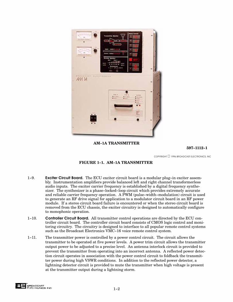
FIGURE 1-1. AM-1A TRANSMITTER
597-1112-1
COPYRIGHT 1996 BROADCAST ELECTRONICS, INC
AM-1A TRANSMITTER
1-9. Exciter Circuit Board. The ECU exciter circuit board is a modular plug-in exciter assem�bly. Instrumentation amplifiers provide balanced left and right channel transformerlessaudio inputs. The exciter carrier frequency is established by a digital frequency synthe�sizer. The synthesizer is a phase-locked-loop circuit which provides extremely accurateand reliable carrier frequency operation. A PWM (pulse-width-modulation) circuit is usedto generate an RF drive signal for application to a modulator circuit board in an RF powermodule. If a stereo circuit board failure is encountered or when the stereo circuit board isremoved from the ECU chassis, the exciter circuitry is designed to automatically configureto monophonic operation.
1-10. Controller Circuit Board. All transmitter control operations are directed by the ECU con�troller circuit board. The controller circuit board consists of CMOS logic control and moni�toring circuitry. The circuitry is designed to interface to all popular remote control systemssuch as the Broadcast Electronics VMC-16 voice remote control system.
1-11. The transmitter power is controlled by a power control circuit. The circuit allows the
transmitter to be operated at five power levels. A power trim circuit allows the transmitter
output power to be adjusted to a precise level. An antenna interlock circuit is provided to
prevent the transmitter from operating into an incorrect antenna. A reflected power detec�
tion circuit operates in association with the power control circuit to foldback the transmit�
ter power during high VSWR conditions. In addition to the reflected power detector, a
lightning detector circuit is provided to mute the transmitter when high voltage is present
at the transmitter output during a lightning storm.
1-3
1-12. OUTPUT NETWORK CHASSIS. The output network chassis contains: 1) a bandpass filter,
2) an RF power module, 3) a power supply circuit board, 4) a lightning detection circuit
board, 5) a lightning protection circuit board, and 6) a directional coupler assembly. The
bandpass filter is provided to attenuate all harmonic frequencies to FCC, DOC, and CCIR
levels.
1-13. RF Power Module. Each transmitter is equipped with a single RF power module. Thepower module is a modular plug-in assembly containing two RF power amplifier circuitboards and one modulator circuit board. The AM-1A power module will produce 1100watts of RF power. The AM-500A power module will produce 550 watts of RF power.
1-14. The RF power module is designed using Class E amplifier technology. A Class E amplifier
exhibits high efficiency and provides superior audio performance. In addition to the supe�
rior efficiency and audio performance, the power module is designed to be removed from
the chassis for maintenance.
1-15. Power Supply. A modular switching power supply provides dc operating potentials for thetransmitter. The power supply design uses an SCR controlled bridge to rectify the ac linevoltage into a dc potential. The supply is filtered and routed to the RF power module forcontrol and regulation. A fault detection circuit monitors power supply activity for failureconditions. A separate modular switching power supply provides operating potentials forthe ECU circuitry.
1-16. TRANSMITTER CONFIGURATIONS.
1-17. The transmitters can be ordered in the following configurations:
P/N DESCRIPTION
907-1000-001 AM-1A 1 kW AM Transmitter for operation
in the 522 kHz to 1705 kHz broadcast band,
196V - 252V ac 50/60 Hz single phase supply.
907-0500-001 AM-500A 500W AM Transmitter for operation
in the 522 kHz to 1705 kHz broadcast band,
196V - 252V ac 50/60 Hz single phase supply.
1-18. ACCESSORIES AND SPARE PARTS KITS.
1-19. The following text presents accessories and spare parts kits available for use with the
AM-1A/AM-500A transmitters.
P/N DESCRIPTION
977-0027 Recommended semiconductor kit.
977-0028 100% semiconductor kit.
977-0029 Recommended spare parts kit. Includes selected
meters, switches, fuses, filters, etc. Does not
include semiconductors.
977-0037 Basic semiconductor kit for AM-A series, AM-1A,
AM-6A, AM-10A.
1-20. EQUIPMENT SPECIFICATIONS.
1-21. Refer to Table 1-1 for electrical specifications or Table 1-2 for physical specifications of the
AM-1A/AM-500A transmitter.
1-4
TABLE 1-1. ELECTRICAL CHARACTERISTICS
(Sheet 1 of 3)
PARAMETER SPECIFICATION
RF POWER OUTPUT
AM-1A 5 watts to 1100 watts. Five preset power levels
available by local or remote control.
AM-500A 5 watts to 550 watts. Five preset power levels
available by local or remote control.
RF CARRIER FREQUENCY 522 kHz to 1705 kHz (as ordered).
RANGE Accommodates 9 kHz or 10 kHz channel spacing
(9 kHz spacing requires an optional crystal).
RF OUTPUT IMPEDANCE 50 Ohms, unbalanced.
OUTPUT CONNECTOR Type N Connector.
LOAD VSWR 1.30 : 1 at full carrier power. Will operate into a
higher VSWR with automatic power reduction.
Open and short circuit protected. Load VSWRs
higher than 1.30 : 1 are accommodated with an
optional matching network.
HARMONIC AND SPURIOUS Meets or exceeds FCC, DOC, and CCIR require-
SUPPRESSION ments when preceded by external NRSC-1 com-
patible audio low-pass filters.
CARRIER FREQUENCY ±3ppm, 0° to 50° C (+32° to +122° F).
STABILITY
CARRIER SHIFT Less than 1% at 95% negative modulation at
1 kHz.
TYPE OF MODULATION Pulse Width Modulation of L+R envelope with
integrated C-QUAM AM stereo. An RF input
connector is also provided for an external stereo
exciter.
OPERATING MODES Stereo, mono L+R, mono L, mono R, by local or
remote control.
MODULATION CAPABILITY
AM-1A Greater than 145% peak positive capability at
1100 watts. 130% into a 1.5 : 1 VSWR.
AM-500A Greater than 145% peak positive capability at
500 watts. 130% into a 1.3 : 1 VSWR.
MODULATION INPUT Peak reading, color coded, LED bar graph display
INDICATION with an autorange feature for monitoring positive
or negative input levels of four different audio
channels (L/R or L+R/L-R).
AUDIO INPUT LEVEL +10 dBm, ±1 dB, L+R (or mono) to produce 100%
L+R envelope modulation. Other input levels can
be accommodated.

1-5
TABLE 1-1. ELECTRICAL CHARACTERISTICS
(Sheet 2 of 3)
PARAMETER SPECIFICATION
AUDIO INPUT IMPEDANCE 600 Ohms. Inputs are balanced, transformerless,
and resistive with passive RFI filtering. Other
impedances can be accommodated.
AUDIO FREQUENCY RESPONSE
(MONOPHONIC)
AM-1A ±0.5 dB, 20 Hz to 10 kHz at 90% negative
modulation (linear phase mode). +0.1 dB
-3 dB, 20 Hz to 10 kHz at 90% negative
modulation, standard configuration. 90%
negative modulation referenced at 1 kHz (9 dBm).
AM-500A ±1.0 dB, 20 Hz to 10 kHz at 90% negative
modulation (linear phase mode). +0.1 dB
-3 dB, 20 Hz to 10 kHz at 90% negative
modulation, standard configuration. 90%
negative modulation referenced at 1 kHz (9 dBm).
AUDIO HARMONIC DISTORTION
AM-1A Mono Less than 0.8%, 20 Hz to 10 kHz at 1 kW.
Less than 1.5%, 20 Hz to 10 kHz at 500 W.
Less than 2.0%, 20 Hz to 10 kHz at 250 W.
Less than 3.0%, 20 Hz to 10 kHz at 100 W.
The mono audio harmonic distortion
specifications are referenced to an audio input
level which generates 90% modulation at 1 kHz
(9 dBm).
AM-1A Stereo Less than 1.5% at 50% single channel
modulation, 50 Hz to 10 kHz at rated power.
AM-500A Mono Less than 1.2%, 20 Hz to 10 kHz at 500 Watts.
The mono audio harmonic distortion
specifications are referenced to an audio input
level which generates 90% modulation at 1 kHz
(9 dBm).
AM-500A Stereo Less than 2.0% at 50% single channel
modulation, 50 Hz to 10 kHz at rated power.
INTERMODULATION DISTORTION 1.2% or less at 1:1 ratio. 1.7% or less at 4:1 ratio.
(MONO) 60/7000 Hz SMPTE standards with 85%
modulation at rated power.
CCIF INTERMODULATION 1.0% or less at 1:1 ratio. 4 kHz/5 kHz with 85%
DISTORTION (MONO) modulation at rated power.
TRANSIENT INTERMODULATION 1.0% or less at 4:1 ratio. 2.96 kHz square wave
DISTORTION (MONO) 8 kHz sinewave with 85% modulation at rated
power.

1-6
TABLE 1-1. ELECTRICAL CHARACTERISTICS
(Sheet 3 of 3)
PARAMETER SPECIFICATION
INCIDENTAL PHASE 30 dB below equivalent 100% L-R C-QUAM
MODULATION modulation 50 Hz to 10 kHz at rated power.
(STEREOPHONIC) Measured with an audio input level which
generates 95% negative L+R envelope modulation
at 1 kHz (9.5 dBm).
STEREO SEPARATION
AM-1A -30 dB or greater, 50 Hz to 10 kHz. Measured
with 50% single channel modulation into a 50
ohm resistive load at rated power.
AM-500A -25 dB or greater, 50 Hz to 10 kHz. Measured
with 50% single channel modulation into a 50
ohm resistive load at rated power.
SQUAREWAVE OVERSHOOT
Mono 0.1% or less at 400 Hz, 90% modulation with high
frequency boost disabled.
Stereo 1% or less at 400 Hz, 50% single channel modula-
tion with high frequency boost disabled.
SQUAREWAVE TILT Less than 1% at 40 Hz. Less than 1.5% at 20 Hz.
Measured with 90% negative modulation.
NOISE
Mono Greater than 65 dB below a reference level equiva-
lent to 100% negative modulation in a 22 Hz to
30 kHz bandwidth, unweighed.
Stereo Greater than 55 dB below a reference level equiva-
lent to 100% negative modulation of either left or
right channel in a 22 Hz to 30 kHz bandwidth,
unweighed.
AC INPUT VOLTAGE 196V to 252V ac, 50/60 Hz, single phase. Includes
built-in MOVs for surge suppression.
AC POWER CONSUMPTION
AM-1A 1.37 kW, no modulation of 1 kW carrier.
2.05 kW, 100% sinusoidal modulation of 1 kW
carrier.
Measured at 1 kW into a 50 Ohm resistive load at
220V ac.
AM-500A 830 watts, no modulation of 500 watt carrier.
1.25 kW, 100% sinusodial modulation of 500 Watt
carrier. Measured at 500 watts into a 50 Ohm
resistive load at 220V ac.
1-7
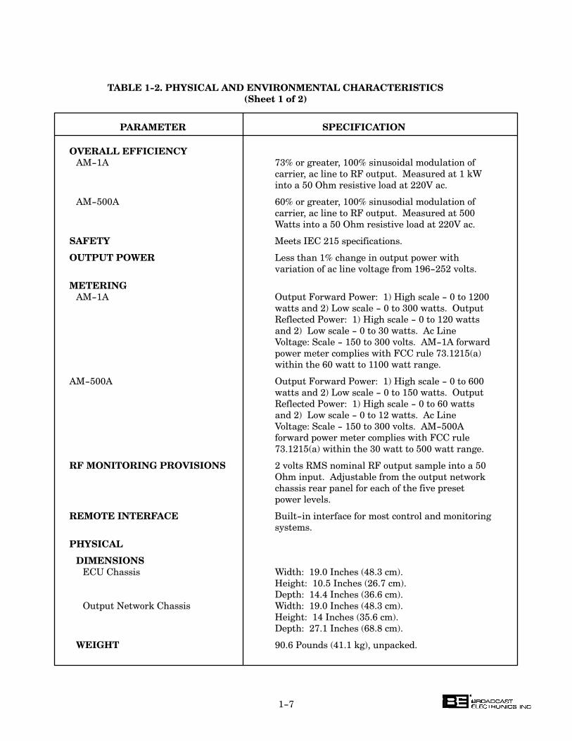
TABLE 1-2. PHYSICAL AND ENVIRONMENTAL CHARACTERISTICS
(Sheet 1 of 2)
PARAMETER SPECIFICATION
OVERALL EFFICIENCY
AM-1A 73% or greater, 100% sinusoidal modulation of
carrier, ac line to RF output. Measured at 1 kW
into a 50 Ohm resistive load at 220V ac.
AM-500A 60% or greater, 100% sinusodial modulation of
carrier, ac line to RF output. Measured at 500
Watts into a 50 Ohm resistive load at 220V ac.
SAFETY Meets IEC 215 specifications.
OUTPUT POWER Less than 1% change in output power with
variation of ac line voltage from 196-252 volts.
METERING
AM-1A Output Forward Power: 1) High scale - 0 to 1200
watts and 2) Low scale - 0 to 300 watts. Output
Reflected Power: 1) High scale - 0 to 120 watts
and 2) Low scale - 0 to 30 watts. Ac Line
Voltage: Scale - 150 to 300 volts. AM-1A forward
power meter complies with FCC rule 73.1215(a)
within the 60 watt to 1100 watt range.
AM-500A Output Forward Power: 1) High scale - 0 to 600
watts and 2) Low scale - 0 to 150 watts. Output
Reflected Power: 1) High scale - 0 to 60 watts
and 2) Low scale - 0 to 12 watts. Ac Line
Voltage: Scale - 150 to 300 volts. AM-500A
forward power meter complies with FCC rule
73.1215(a) within the 30 watt to 500 watt range.
RF MONITORING PROVISIONS 2 volts RMS nominal RF output sample into a 50
Ohm input. Adjustable from the output network
chassis rear panel for each of the five preset
power levels.
REMOTE INTERFACE Built-in interface for most control and monitoring
systems.
PHYSICAL
DIMENSIONS
ECU Chassis Width: 19.0 Inches (48.3 cm).
Height: 10.5 Inches (26.7 cm).
Depth: 14.4 Inches (36.6 cm).
Output Network Chassis Width: 19.0 Inches (48.3 cm).
Height: 14 Inches (35.6 cm).
Depth: 27.1 Inches (68.8 cm).
WEIGHT 90.6 Pounds (41.1 kg), unpacked.

1-8
TABLE 1-2. PHYSICAL AND ENVIRONMENTAL CHARACTERISTICS
(Sheet 2 of 2)
PARAMETER SPECIFICATION
CUBAGE 7.3 Ft3(0.21 m3).
ENVIRONMENTAL
COOLING Low velocity air with cleanable filters. 250 Cubic
Feet Per Minute (7.08 m3/min).
OPERATING TEMPERATURE 0° to 50° C (+32° to +122° F).
OPERATING HUMIDITY 0 to 95% (non-condensing).
MAXIMUM ALTITUDE
60 Hz Models 0 to 10,000 feet above sea level (0 to 3048 Meters).
50 Hz Models 0 to 7,500 feet above sea level (0 to 2286 Meters).
NOTE - AM-500A - All specifications measured at 500 watts into a 50 ohm resistive load using
Broadcast Electronics AS-10 modulation monitor.
AM-1A - All specifications measured at 1100 watts into a 50 ohm resistive load using
Broadcast Electronics AS-10 modulation monitor.

2-1
SECTION II
INSTALLATION
2-1. INTRODUCTION.
2-2. This section contains information required for the installation and preliminary checkout of
the Broadcast Electronics AM-1A/AM-500A transmitters.
2-3. UNPACKING.
2-4. The equipment becomes the property of the customer when the equipment is delivered to
the carrier. Carefully unpack the transmitter. Perform a visual inspection to determine
that no apparent damage has been incurred during shipment. All shipping materials
should be retained until it is determined that the unit has not been damaged. Claims for
damaged equipment must be promptly filed with the carrier or the carrier may not accept
the claim.
2-5. The contents of the shipment should be as indicated on the packing list. If the contents are
incomplete, or if the unit is damaged electrically or mechanically, notify both the carrier
and Broadcast Electronics.
2-6. ENVIRONMENTAL REQUIREMENTS.
2-7. Table 1-2 provides environmental conditions which must be considered prior to transmit�
ter installation. Refer to Table 1-2 in SECTION I, INTRODUCTION and ensure the
transmitter is to be installed in an acceptable environment.
2-8. INSTALLATION.
2-9. Each transmitter is wired, operated, tested, and inspected at the factory prior to shipment
and is ready for installation when received. Prior to installation, this publication should be
studied to obtain an understanding of the operation, circuitry, nomenclature, and installa�
tion requirements. Installation is accomplished as follows: 1) placement, 2) component
installation, 3) circuit board programming, 4) remote control connections, 5) wiring,
6) transmitter site lightning protection system checkout, 7) initial checkout, and 8) prelimi�
nary operation and adjustment.
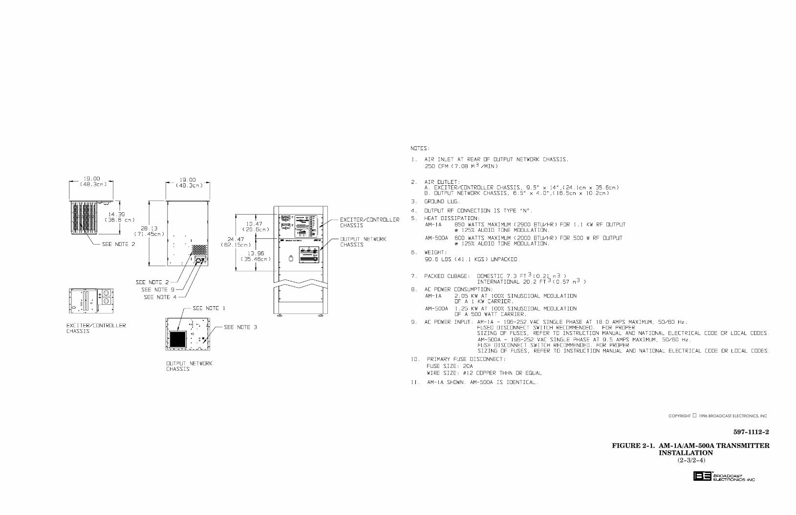
2-10. EQUIPMENT PLACEMENT.
2-11. The AM-1A/AM-500A transmitter is designed for placement in a 19 inch EIA rack assem�
bly (refer to Figure 2-1). The transmitter requires approximately 24.5 inches (62.2 cm) of
a universal or military EIA rack (refer to Figure 2-2). To install the transmitter in a rack,
refer to Figure 2-2 and perform the following procedures.
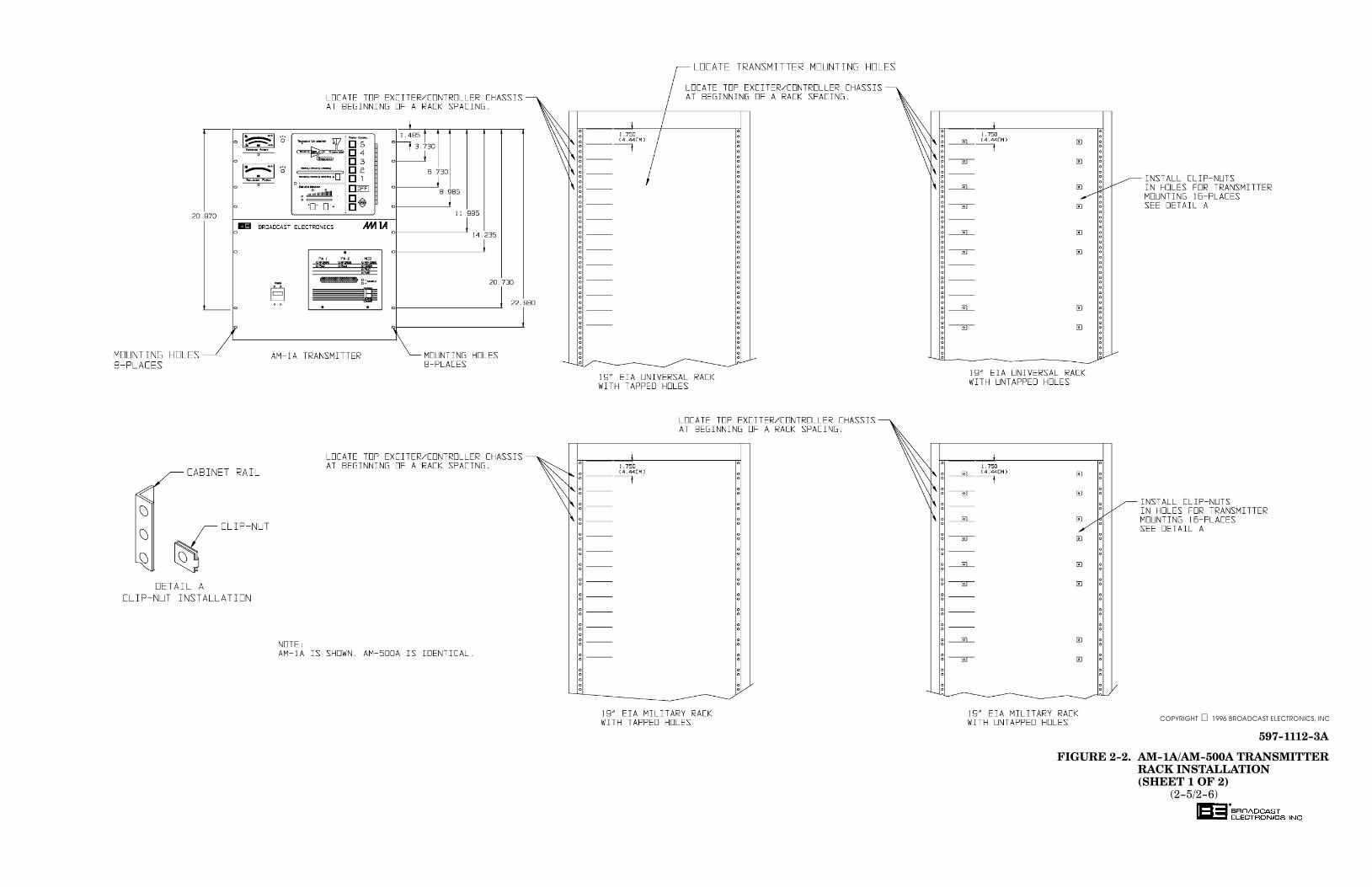
2-12. RACK PREPARATION. The transmitter can be mounted in any universal or military rack
assembly. Refer to Figure 2-2 and determine type of rack for transmitter installation. A
universal rack is identified by the location of mounting holes at regular rack spacings. A
military rack is identified by a missing mounting hole at regular rack spacings. Each type
of rack may be equipped with untapped or tapped mounting holes. To prepare the rack for
the transmitter, refer to Figure 2-2 and perform the following procedure.
2-13. Prepare a universal or military rack for transmitter installation as follows:
1. Refer to Figure 2-2 and locate the transmitter mounting holes on the rack assem-
bly. Ensure the top of the transmitter is located at the beginning of a rack unit.
2-2
2. Evaluate the rack and determine if the rack is equipped with tapped or untapped
mounting holes.
3. Prepare the rack for installation as follows:
A. For racks with tapped holes, mark the transmitter mounting hole locations.
B. For racks with untapped holes, locate the transmitter clip-nuts in the
transmitter accessory kit. Refer to Figure 2-2 and install the clip-nuts in
each transmitter mounting hole location.
WARNING
WARNING
ENSURE NO PRIMARY POWER IS CONNECTED TO THE TRANSMITTER BEFORE PROCEEDING.
2-14. EQUIPMENT INSTALLATION.
2-15. TRANSMITTER MOUNTING. Once the transmitter rack is prepared, refer to Figure 2-2
and mount the transmitter in the rack by performing the following procedures.
2-16. The transmitter accessory kit contains #10 x 3/4 and #12 x 3/4 mounting hardware. The
type of hardware used to install the transmitter is determined by the rack assembly. Refer
to Figure 2-2 and determine the mounting hardware required to mount the transmitter in
the rack.
2-17. Install the ECU chassis and the output network chassis in rack as follows:
1. Insert the ECU chassis in the rack and install the appropriate hardware in two
mounting locations to secure the chassis in the rack.
WARNING
WARNING
ENSURE THE GROUND STRAP IS CONNECTED
BETWEEN THE ECU CHASSIS AND THE OUTPUT
NETWORK CHASSIS.
2. Install the ground straps between the ECU and the output network chassis as
shown. The straps are to be placed just in front of the rack P-rail and secured
using the front panel mounting hardware.
3. Insert the output network chassis in the rack and install the appropriate hardware
in two mounting locations to secure the chassis in the rack.
4. Using the appropriate hardware, install the remaining hardware to secure the
chassis units in the rack.
2-18. Connect the ECU control cables as follows:
1. Attach connector J4 to P4 on the ECU chassis.
2. Attach connector J5 to P5 on the ECU chassis.
3. Attach connector J501 to P501 on the meter circuit board.
597-1112-2
FIGURE 2-1. AM-1A/AM-500A TRANSMITTERINSTALLATION
(2-3/2-4)
COPYRIGHT 1996 BROADCAST ELECTRONICS, INC
597-1112-3A
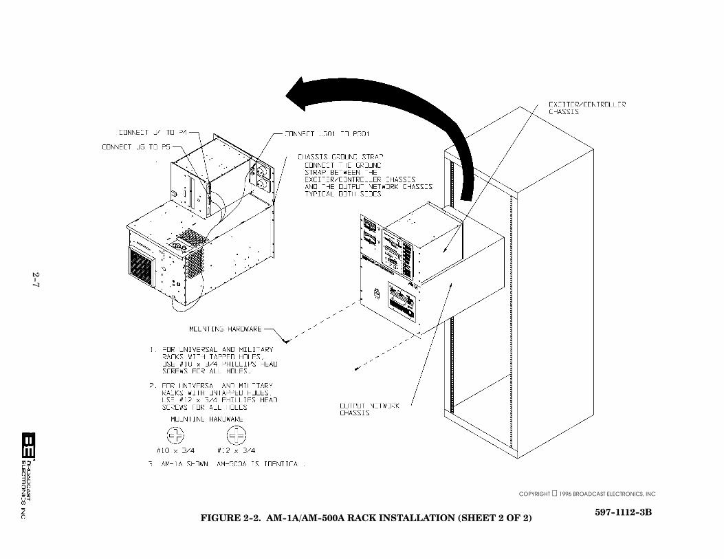
FIGURE 2-2. AM-1A/AM-500A TRANSMITTERRACK INSTALLATION(SHEET 1 OF 2)
(2-5/2-6)
COPYRIGHT 1996 BROADCAST ELECTRONICS, INC
2-7
COPYRIGHT 1996 BROADCAST ELECTRONICS, INC
597-1112-3BFIGURE 2-2. AM-1A/AM-500A RACK INSTALLATION (SHEET 2 OF 2)

2-8
2-19. COMPONENT INSTALLATION.
WARNING
WARNING
ENSURE NO PRIMARY POWER IS CONNECTED TO
THE TRANSMITTER BEFORE PROCEEDING.
2-20. Selected transmitter components have been removed to prevent damage during shipment.
The components removed from the transmitter are shipped in separate containers.
2-21. Remove all tape, wire ties, string, and packing material used for shipment. In addition,
locate the component containers. To install the components, perform the following proce�
dures.
2-22. ECU CIRCUIT BOARDS. The ECU circuit boards are removed for shipment. Locate the
shipping container with the ECU circuit boards. To re-install the circuit boards, proceed
as follows:
CAUTION
CAUTION
THE TRANSMITTER MAY BE DAMAGED IF THE ECU CIRCUIT BOARDS ARE NOT SECURELY SEATED INTOTHE CONNECTORS.
1. Refer to Figure 2-3 to determine the circuit board location.
2. Insert the circuit board in the appropriate location.
3. Firmly press the circuit board into the connector to engage the connector
housing.
4. Firmly press the circuit board into the connector again to engage the connector
pins.
5. Repeat the procedure for each ECU circuit board.
CAUTION
CAUTION
REMOVING OR INSTALLING THE RF POWER MODULEWITH THE TRANSMITTER ENERGIZED MAY RESULTIN DAMAGE TO THE MODULE.
2-23. RF POWER MODULE. The RF power module is removed for shipment. Locate the RF
power module shipping container. Refer to Figure 2-3 and re-install the module.
2-24. BATTERY INSTALLATION. The ECU is equipped with a battery system. Refer to Figure
2-3 and install the battery in the battery receptacle.
2-25. CIRCUIT BOARD PROGRAMMING.
2-26. The AM-1A/AM-500A transmitters are designed with programmable transmitter operat�
ing characteristics. The operating characteristics are determined by the programmable
circuitry on the ECU circuit boards. Refer to the following text and program the circuitry
for the desired operating characteristics.

2-9
FIGURE 2-3. COMPONENT INSTALLATION
597-1112-4
COPYRIGHT 1996 BROADCAST ELECTRONICS, INC

2-10
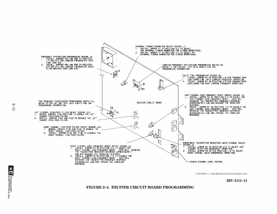
2-27. EXCITER CIRCUIT BOARD. Exciter circuit board programming is presented in Figure 2-4.
Refer to Figure 2-4 and program the circuit board as required.
2-28. External Stereo Generator Select. Programmable header J7 programs the circuitry if: 1) an external stereo generator is to be used with the transmitter or 2) the internal stereocircuit board is to be used with the transmitter. The transmitter is shipped with the circuitprogrammed for internal stereo circuit board operation.
2-29. Carrier Frequency Programming. Eight position switch S2 programs the exciter carrierfrequency. The switch is programmed for the station frequency at the factory. Refer to thefactory test data sheets to check the programming of the switch. If the switch program�ming is not identical to programming recorded in the factory test data sheets, contact theBroadcast Electronics Customer Service Department.
2-30. PWM Frequency Programming. Four position switch S1 programs the PWM frequency.Refer to the factory test data sheets to check the programming of the switch.
2-31. Frequency Synthesizer Programming. Programmable header J6 determines the frequencysynthesizer band of operation. Refer to the factory test data sheets to check the program�ming of the header.
2-32. Pilot Tone Programming. Programmable header J5 establishes the pilot tone frequency for10 kHz carrier frequency operation and 9 kHz carrier frequency operation. Refer to thefactory test data sheets to check the programming of the header.
2-33. High-Pass Filter Defeat. Left channel programmable header J12 and right channel pro�grammable header J13 control an exciter second order 10 Hz high-pass filter. The high-pass filter is provided to remove low frequency residual products from specific audio proc�essing units. The filter is shipped from the factory in the enabled position. Evaluate theaudio processor and determine if low frequency residual products are present at the outputof the audio processing unit. If no low frequency residual products are present, refer toFigure 2-4 and disable the high pass filter.
2-34. High Frequency Boost Defeat. Left channel programmable header J2 and right channelprogrammable header J3 control an exciter high frequency boost circuit. The high fre�quency boost circuit provides increased high frequency response to compensate for a Besselfilter in the PWM modulator. If the high frequency boost circuit is enabled to compensatefor the filter, the circuit will result in a compromise between the frequency and transientresponse performance. If the high frequency boost circuit is enabled, the transmitter fre�quency response will increase approximately 2 dB at 10 kHz and the transient responsewill degrade. If the high frequency boost circuit is disabled, the transmitter frequency re�sponse will decrease approximately 2 dB at 10 kHz and the transient response will im�prove. The high frequency boost circuit is shipped from the factory in the disabled posi�tion.
2-35. Monophonic Transmitter Operation Channel Select. Programmable header J4 selectseither the left or right audio channel when the transmitter is operating in the monophonicmode with the stereo circuit board removed. The transmitter is shipped with the left chan�nel audio selected for monophonic operations.
2-36. STEREO CIRCUIT BOARD. Stereo circuit board programming is presented in Figure 2-5.
Refer to Figure 2-5 and program the circuit board as required.
2-37. Antenna C Equalization Select. Programmable header J6 selects equalization circuit 1 orequalization circuit 2 for operation with antenna C. The transmitter is shipped withequalization circuit 2 configured for operation with antenna C.
2-38. Bandpass Filter Alignment. Programmable header J5 configures the bandpass filter foralignment. The jumper must be installed in position 1-2.
2-39. Bandpass Filter Programming. Four position switches S2 through S4 program the band�pass filter. Refer to the factory test data sheets to check the programming of the switches.
2-40. Equalization Control Select. Programmable header J7 configures the equalization cir�cuitry for either a momentary or constant antenna status signal. The transmitter isshipped with the equalization control circuitry configured for a constant status signal.
2-11
COPYRIGHT 1993 BROADCAST ELECTRONICS, INC
597-1111-11
FIGURE 2-4. EXCITER CIRCUIT BOARD PROGRAMMING

2-12
COPYRIGHT 1993 BROADCAST ELECTRONICS, INC
597-1111-6
FIGURE 2-5. STEREO CIRCUIT BOARD PROGRAMMING
2-13
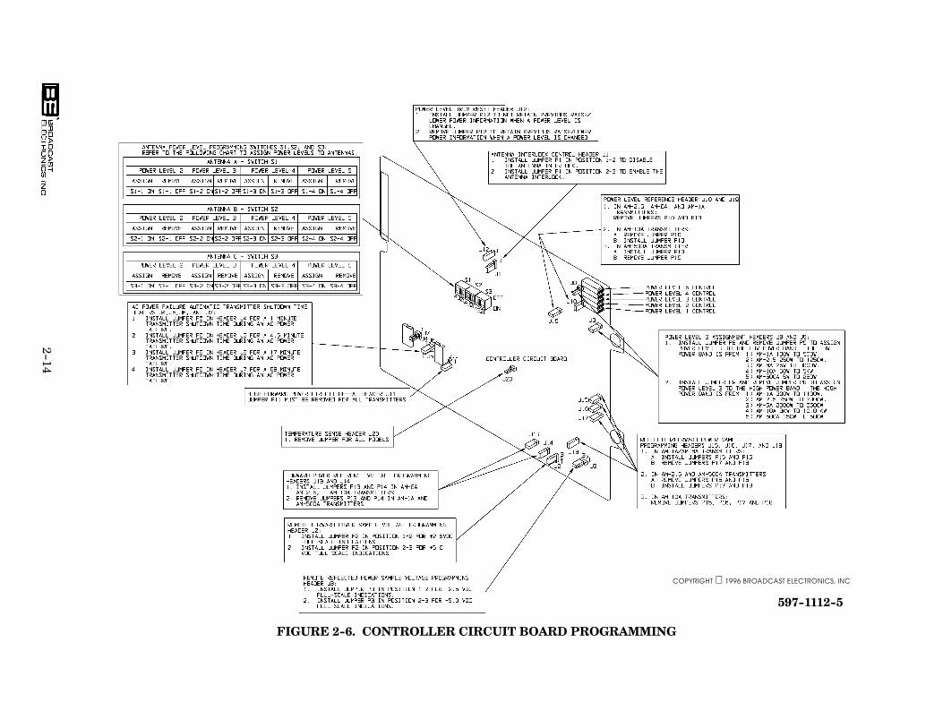
2-41. CONTROLLER CIRCUIT BOARD. Controller circuit board programming is presented in
Figure 2-6. Refer to Figure 2-6 and program the circuit board as required.
2-42. Power Level Trim Reset Select. Programmable header J12 determines if the power levelcontrol circuit is to reset when a power level switch/indicator is depressed. If the circuit isprogrammed to reset, the previous raise/lower information will be deleted and the trans�mitter will operate at the selected power level. If the circuit is programmed to retain theprevious raise/lower information, the transmitter will operate above or below the selectedpower level as determined by previous raise/lower operations. For example, the transmit�ter is operating at power level 4 with the power level raised 5% by the raise/lower circuit.When power level 5 switch/indicator is depressed, the transmitter will operate at 5% abovethe power level 5 output due to the previously retained raise/lower information. The trans�mitter is shipped with power level trim reset circuit configured to reset.
2-43. Antenna Power Level Programming. Switches S1, S2, and S3 assign power levels to a spe�cific antenna. This programs the antenna interlock circuit to the station antenna systemto prevent the transmitter from operating into an antenna at an incorrect power level.Switch S1 programs the power levels for antenna A. Switch S2 programs the power levelsfor antenna B. Switch S3 programs the power levels for antenna C. Power level 2 is as�signed to an antenna by switch 1 on S1, S2, and S3. Power level 3 is assigned to an an�tenna by switch 2 on S1, S2, and S3. Power level 4 is assigned to an antenna by switch 3on S1, S2, and S3. Power level 5 is assigned to an antenna by switch 4 on S1, S2, and S3.Power level 1 is assigned to each antenna. Evaluate the antenna system and program thecircuit as required.
2-44. AC Power Failure Automatic Transmitter Shutdown Time. Programmable headers J4, J5,J6, and J7 program the transmitter ac power failure automatic transmitter shutdowntimer circuit. The circuit is designed to automatically operate the transmitter to off duringa power failure after a specific time delay programmed by headers J4, J5, J6, and J7. J4programs the circuit for a 1 minute shutdown time. J5 programs the circuit for a 4.5 min�ute shutdown time. J6 programs the circuit for a 17 minute shutdown time. J7 programsthe circuit for a 68 minute shutdown time. The transmitter is shipped from the factory fora 1 minute shutdown time.
2-45. Antenna Interlock Control Select. Programmable header J1 controls the antenna inter�lock circuit. The circuit can be disabled if the transmitter is to operate into only one an�tenna. The transmitter is shipped from the factory with the antenna interlock circuit dis�abled.
2-46. Power Level Reference. Programmable headers J10 and J19 provide a reference for thepower level circuit. For AM-1A models, ensure jumpers P10 and P19 are removed. ForAM-500A models, ensure jumper P10 is installed and P19 is removed.
2-47. Power Level 3 Assignment. Programmable headers J8 and J9 control the power level as�signment for the power level 3 switch/indicator. For AM-1A transmitters, the power level3 switch/indicator can be programmed to control power from: 1) 100 watts to 500 watts or2) 300 watts to 1100 watts. The power level 3 switch/indicator is shipped from the factoryto control power from 100 watts to 500 watts. Program jumpers P8 and P9 as required.For AM-500A transmitters, the power level 3 switch/indicator can be programmed to con�trol power from: 1) 5 watts to 250 watts or 2) 150 watts to 500 watts. The power level 3switch/indicator is shipped from the factory to control power from 150 watts to 500 watts.Program jumpers P8 and P9 as required.
2-48. Remote Reflected Power Sample Voltage Programming. Programmable header J3 con�trols the remote reflected power meter sample voltage. The remote reflected power samplecan be programmed for +5.0 volt dc or +2.5 volt dc full-scale meter indications. The trans�mitter is shipped from the factory programmed for +5.0 volt dc full-scale remote reflectedpower meter indications.
2-14
COPYRIGHT 1996 BROADCAST ELECTRONICS, INC
597-1112-5
FIGURE 2-6. CONTROLLER CIRCUIT BOARD PROGRAMMING

2-15
2-49. Remote Forward Power Sample Voltage Programming. Programmable header J2 con�trols the remote forward power meter sample voltage. The remote forward power samplecan be programmed for +5.0 volt dc or +2.5 volt dc full-scale meter indications. The trans�mitter is shipped from the factory programmed for +5.0 volt dc full-scale remote forwardpower meter indications.
2-50. High Forward Power Defeat. Programmable header J11 controls the high forward powerdetector circuit. Ensure jumper P11 is removed.
2-51. Reflected/Forward Power Sample Programming. Programmable headers J15, J16, J17,and J18 control the reflected and forward power sample levels. Headers J15 and J17 con�trol the forward power sample. Headers J16 and J18 control the reflected power sample.For AM-1A models, ensure: 1) jumpers P15 and P16 are installed and 2) jumpers P17 andP18 are removed. For AM-500A models, ensure: 1) jumpers P15 and P16 are removedand 2) jumpers P17 and P18 are installed.
2-52. Forward Power Reference Voltage Programming. Programmable headers J13 and J14establish the forward power reference level for a comparator circuit. Ensure jumpers P13and P14 are removed.
2-53. Temperature Sense. Header J20 controls the temperature sense sample voltage. EnsureP20 is removed for all models.
2-54. POWER SUPPLY CIRCUIT BOARD. The power supply circuit board programming is pre�
sented in the following text. Refer to the following text to check the power supply circuit
board programming.
2-55. Future Corrector Circuit. Programmable headers J9 and J10 establish parameters for afuture corrector circuit. Ensure jumpers P9 is removed and P10 is installed.
2-56. Model Programming. Programmable headers J5 through J8 establish parameters for dif�ferent AM A-Series transmitters. Refer to the following text for the programming infor�mation.
TRANSMITTER J5 J6 J7 J8
AM-1A Install Remove Remove Install
AM-500A Install Remove Install Install
2-57. REMOTE CONTROL CONNECTIONS.
WARNING
WARNING
ENSURE PRIMARY POWER IS DISCONNECTED BE�
FORE PROCEEDING.
2-58. GENERAL. The AM-1A/AM-500A transmitters are designed for complete remote control
operation (refer to Figure 2-7). The transmitter will interface with almost any remote con�
trol unit such as the Broadcast Electronics model VMC-16 voice remote control system.
The following text presents a description of the transmitter remote control functions and
indications. The remote control functions are activated using a +5 to +15 volt dc signal.
The remote indication functions: 1) require current limiting resistors and 2) provide up to
100 mA for indicators. A +5 volt supply is provided on the ECU rear-panel for remote con�
trol operations. The remote control connections are located on the rear-panel of the ECU.
2-59. Power Level Controls/Indicators. The transmitter is designed with five customer adjust�able operating power controls. The controls are located at TB1-1 through TB1-5. A +5 to+15 volt dc signal is required to activate the desired function.
2-60. Indications of power level control operations are located at TB1-7 through TB1-11. The
power level status indicators will go LOW (0 volts dc) when activated.
2-61. Transmitter Off Control/Indicator. The transmitter off control is located at TB1-6. A +5 to+15 volt dc signal is required to operate the transmitter to off. The transmitter off controlindicator is located at TB1-12. The off indicator will go LOW (0 volts dc) when activated.
2-16
COPYRIGHT 1996 BROADCAST ELECTRONICS, INC
597-1112-3
FIGURE 2-7. REMOTE CONTROL AND AUDIO CONNECTIONS

2-17
2-62. Power Level Raise/Lower Controls. The transmitter is designed with raise and lower con�trols to adjust the transmitter output power level. The controls are equipped with the abil�ity to raise/lower power from 10% to 15% of the selected output power level. The controlsare located at TB1-16 and TB1-17. A +5 to +15 volt dc signal is required to activate thedesired function.
2-63. Antenna Interlock Input. The antenna interlock inputs are designed for the connection ofthe status signals from antenna A, B, and C. The inputs are located at TB1-24 throughTB1-26. The inputs require a +5 to +15 volt dc signal to indicate an antenna ready status.
2-64. Transmitter Mute Input. The transmitter mute input is designed to mute the transmitterwhen activated. The input is located at TB1-27. The input requires a +5 to +15 volt dcsignal to mute the transmitter.
2-65. Remote Failsafe Input. The remote failsafe input is designed for the remote control unitfailsafe control line. The input is located at TB1-28. The input requires a +5 to +15 voltdc signal to indicate an enabled remote control unit.
2-66. External Interlock Input. The external interlock input is for the connection of an interlockexternal to the transmitter. The input is located at TB1-29. The input requires a +5 to+15 volt dc signal to indicate a closed interlock.
2-67. Interlock +5V. The interlock +5 volt supply is provided for the external interlock. The +5volt supply is located at TB1-30.
2-68. Exciter Mode Controls/Indicators. The transmitter exciter is designed to be configured tomono left, mono right, mono L+R, or stereo modes of operation. The controls are located atTB2-1 through TB2-4. A +5 to +15 volt dc signal is required to activate the desired func�tion.
2-69. Indications of exciter modes of operation are located at TB2-5 though TB2-8. The exciter
mode indicators will go LOW when activated.
2-70. Remote Forward/Reflected Power Meter Indications. Remote reflected/forward powermeter indications are located at TB2-9 and TB2-10. The indications are designed to beprogrammed for +5 volt dc full-scale meter indications or +2.5 volt dc full-scale meter indi�cations.
2-71. Remote Enabled Indications. The remote enabled indicator provides a signal to indicatethe status of transmitter remote control operations. The remote enabled indicator is lo�cated at TB2-11. The indicator will go LOW to indicate when remote control operationsare enabled.
2-72. Antenna Conflict Indications. The antenna conflict indicator provides a signal to indicatewhen the transmitter is configured to operate into an incorrect antenna. The antenna con�flict indicator is located at TB2-12. The indicator will go LOW (0 volts dc) to indicate whenthe transmitter is configured for operation into an incorrect antenna.
2-73. Maintenance Indications. The maintenance indicator provides a signal to indicate whenthe transmitter power supply or RF power module is removed from the transmitter formaintenance. The maintenance indicator is located at TB2-13. The indicator will goLOW (0 volts dc) to indicate when the power supply/RF power module is removed for main�tenance.
2-74. Lightning Indications. For AM-1A models, the lightning indicator provides a signal to in�dicate when a greater than 900 volt potential is present at the output. For AM-500A mod�els, the lightning indicator provides a signal to indicate when a greater than 650 volt po�tential is present at the output. The lightning indicator is located at TB2-14. The indica�tor will go LOW (0 volts dc) to indicate when a lightning potential is present at the trans�mitter output.
2-75. 1.2 : 1 VSWR Indications. The 1.2 : 1 VSWR indicator provides a signal to indicate when agreater than 1.2 : 1 VSWR condition is present at the transmitter output. When this con�dition occurs, the front-panel VSWR indicator will change from green to yellow. The 1.2 : 1indicator is located at TB2-15. The indicator will go LOW (0 volts dc) to indicate when a1.2 : 1 VSWR condition is present at the transmitter output.
2-18
2-76. Exciter/PWR Supply/PWR Module Fault Indications. The exciter, power supply, and powermodule fault indicators provide signals to indicate when an exciter, power supply, or apower module fault has occurred. The exciter, power supply, and power module fault indi�cators are located at TB2-16 through TB2-18. The indicators will go LOW (0 volts dc) toindicate when an exciter, power supply, or a power module fault has occurred.
2-77. RFL PWR High Indications. For AM-1A models, the reflected power high indicator providesa signal to indicate when 40 watts of reflected power is present at the transmitter output.For AM-500A models, the reflected power high indicator provides a signal to indicate when20 watts of reflected power is present at the transmitter output. When this condition oc�curs, the front-panel VSWR indicator will change to red. The high reflected power indica�tor is located at TB2-19. The indicator will go LOW (0 volts dc) to indicate when a re�flected power high condition is present at the transmitter output.
2-78. RFL PWR Emergency Indications. For AM-1A models, the reflected power emergency indi�cator provides a signal to indicate when greater than 200 watts of reflected power is pre�sent at the output of the transmitter. For AM-500A models, the reflected power emergen�cy indicator provides a signal to indicate when greater than 100 watts of reflected power ispresent at the output of the transmitter. When this condition occurs, the front-panelVSWR indicator will flash. The reflected power emergency indicator is located at TB2-20.The indicator will go LOW (0 volts dc) to indicate when a reflected power emergency condi�tion is present at the transmitter output.
2-79. Overtemp Indications. The overtemp indicator provides a signal to indicate when thetransmitter temperature is greater than 57°C. The overtemp indicator is located atTB2-21. The indicator will go LOW (0 volts dc) to indicate when transmitter temperatureis greater than 57°C.
2-80. Foldback Indications. The transmitter is designed to automatically reduce power whenone of the following fault condition occurs: 1) high reflected power, 2) high forward power,3) high temperature, or 4) detection of a high voltage by the lightning circuit. The foldbackindicator is located at TB2-22. The indicator will go LOW (0 volts dc) to indicate when thetransmitter is in a foldback condition.
2-81. Alarm Status Indications. The alarm status provides a signal to indicate when a fault orfoldback condition occurs. The alarm status indicator is located at TB2-23. The indicatorwill go LOW (0 volts dc) to indicate when the transmitter is in a fault or foldback condition.
2-82. Alarm Reset Control. The alarm reset control is designed to reset the fault detection cir�cuitry. The alarm reset control is located at TB2-24. A +5 to +15 volt dc signal is requiredto activate the function.
2-83. WIRING.
2-84. Wiring consists of connecting audio, the RF transmission line, external interlocks, modula�
tion monitor, ground, and ac power to the transmitter. Refer to the following text and con�
nect the wiring to the transmitter.
2-85. AUDIO INPUT CONNECTION. The transmitter is equipped with electronically balanced
600 Ohm left and right channel audio inputs. The audio inputs are located on the ECU
rear-panel (refer to Figure 2-7). The inputs are designed to accept a +10 dBm signal at
600 Ohms.
WARNING
WARNING
ENSURE PRIMARY POWER IS DISCONNECTED BE�
FORE PROCEEDING.
2-86. Audio is interfaced to the transmitter by: 1) selecting the appropriate cable and 2) connect�
ing the cable to the terminals on the ECU rear-panel. To interface audio to the transmit�
ter: 1) use Belden 8760 cable or equivalent and 2) refer to Figure 2-7 and connect the
audio to the transmitter as follows:
2-19
1. Connect the plus signal line to the + terminal.
2. Connect the minus signal line to the - terminal.
3. Connect the shield to ground.
2-87. EXTERNAL STEREO RF INPUT. The transmitter is equipped with an external stereo RF
input on the ECU rear-panel. The input is designed for the connection of an external ste�
reo generator or reference oscillator with a signal level from 5 to 15 volts peak-to-peak. If
an external stereo signal/reference is to be applied to the transmitter, connect the signal to
the J1 EXTERNAL STEREO RF INPUT connector on the ECU rear-panel and program
jumper P7 on the exciter circuit board in position 1-2.
2-88. RF TRANSMISSION LINE CONNECTION. The transmitter RF output receptacle is lo�
cated on the transmitter top-panel (refer to Figure 2-8). The connection requires a Type N
connector. Locate the RF output transmission line and attach the Type N connector to the
RF OUT receptacle on the transmitter.
2-89. EXTERNAL INTERLOCK. The AM-1A/AM-500A transmitter is equipped with an external
interlock such as for a test load. The interlock will operate the transmitter to off when
opened. The interlock is located at TB1-29 and TB1-30 on the rear-panel of the ECU
unit. Refer to External Interlock Input and Interlock +5V in the REMOTE CONTROL
CONNECTIONS section of the preceding text and perform the procedures to connect
equipment to the transmitter external interlock.
597-1112-9
FIGURE 2-8. AM-1A/AM-500A RF OUTPUT AND MODULATION MONITOR CONNECTORS
COPYRIGHT 1996 BROADCAST ELECTRONICS, INC
2-20
2-90. MODULATION MONITOR. The transmitter is equipped with a modulation monitor recep�
tacle. The receptacle is located on the transmitter rear-panel. Refer to Figure 2-8 and
connect the modulation monitor to the MOD MONITOR receptacle.
2-91. AC POWER CONNECTIONS. The AM-1A/AM-500A transmitter requires a single-phase
source of 196V to 252V ac, 50 Hz or 60 Hz at 20 Amperes. AC power is applied to the
transmitter through an ac line cord and modular connector. The transmitter ac power
source must be protected by a 20 Ampere fused disconnect or circuit breaker (refer to Fig�
ure 2-9).
WARNING
WARNING
ENSURE PRIMARY POWER IS DISCONNECTED BE�
FORE PROCEEDING.
2-92. Transmitter AC Line Cord Assembly. AC power is applied to the transmitter using an acline cord and connector. The connector must be assembled to the line cord. To assemblethe modular connector to an ac line cord, proceed as follows:
1. Refer to local electrical codes and select a line cord material for the transmitter ac
line cord assembly. The ac line cord material must contain: 1) minimum 12 gauge
copper conductors and 2) the appropriate insulation type such as S or SO (refer to
Figure 2-9). Determine the length of the cord required to route power to the
transmitter and select the ac line cord material.
2. Locate the modular ac line cord connector in the accessory parts kit.
3. Assemble the ac line cord connector to the ac line cord by following the instructions
contained in the ac line cord connector.
4. Connect the ac line cord to a 196V to 252V ac 50/60 Hz power source protected by a
20 Ampere fused disconnect or circuit breaker.
2-93. Main AC Input. Ensure the transmitter ac line cord is connected to an appropriate powersource. Refer to Figure 2-9 and connect the transmitter ac line cord to the ac input recep�tacle on the top-panel of the output network chassis as shown. Route the line cordthrough the strain relief as shown.
WARNING
WARNING
ENSURE PRIMARY POWER IS DISCONNECTED BE�
FORE PROCEEDING.
WARNING
WARNING
ENSURE AN EARTH GROUND CONDUCTOR IS SE�
CURELY CONNECTED TO THE TRANSMITTER
GROUND LUG.
2-94. GROUND. The transmitter is equipped with a chassis ground system for operating safety.
The ground system requires the connection of an earth ground. Refer to Figure 2-9 and
connect an earth ground to the cabinet ground lug as shown using a 2 inch (5.08 cm) wide
copper strap.
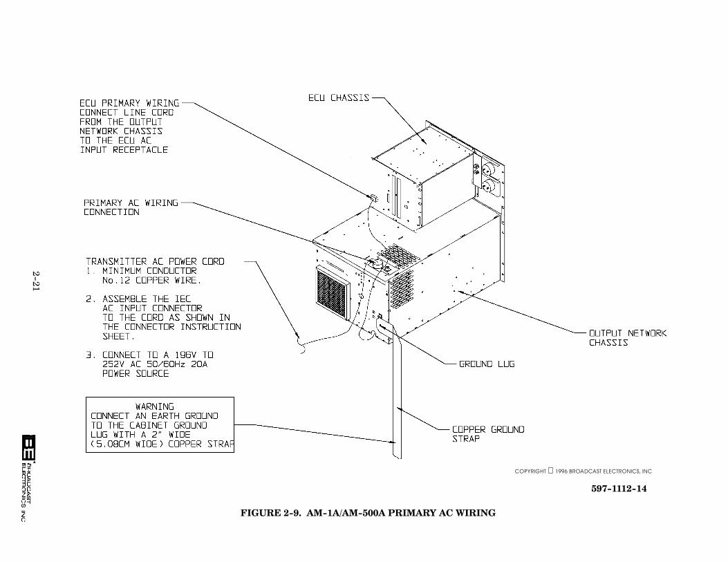
2-21
COPYRIGHT 1996 BROADCAST ELECTRONICS, INC
597-1112-14
FIGURE 2-9. AM-1A/AM-500A PRIMARY AC WIRING

2-22
2-95. TRANSMITTER SITE LIGHTNING PROTECTION SYSTEM CHECKOUT.
CAUTION
CAUTION
THE TRANSMITTER SITE LIGHTNING PROTECTION
SYSTEM MUST BE INSPECTED AND IN PROPER
WORKING CONDITION FOR RELIABLE TRANSMIT�
TER OPERATION.
2-96. For reliable transmitter operation, the transmitter site lightning protection system must
be inspected and in proper working condition. Due to the solid-state design of the trans�
mitter, high voltage potentials from lightning activity can cause severe damage to the
transmitter circuitry. Therefore, perform the following procedures to inspect and improve
the lightning protection system at the transmitter site. Refer to the NAB Radio Handbook
for additional transmitter site lightning protection system information.
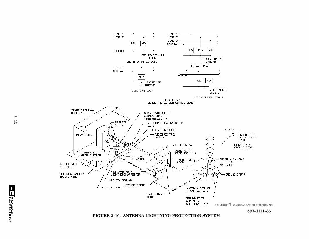
2-97. ANTENNA BALL-GAP LIGHTNING ARRESTOR. Each tower in the antenna system must
be equipped with a ball-gap lightning arrestor (refer to Figure 2-10). The ball-gap arres�
tor is designed to safely conduct lightning potentials to ground. Inspect the ball-gap arres�
tors by performing the following procedures.
2-98. Ball-Gap Position. The antenna ball-gap lightning arrestor must be aligned horizontally.Do not align the ball-gaps vertically. Vertical alignment allows rain water to collect on theballs. This reduces the gap separation and results in arcing during rain activity.
2-99. Ball-Gap Separation. The antenna ball-gap lightning arrestor must be adjusted for theproper separation. If the ball-gap separation is too wide, the arrestor will not function. Ifthe ball-gap separation is too narrow, the arrestor will arc during normal transmitter op�eration. As a general rule: 1) a separation of approximately 0.020 in. for each peak kilo�volt at the transmitter tower is required or 2) 0.125 inch for each 9.4 peak kilovolt at thetransmitter tower is required.
2-100. The recommended method for ball-gap separation adjustment is to adjust the gap to pre�
vent arcing during peak modulation activity. To adjust the separation, proceed as follows:
1. Adjust the ball-gap separation using the general rule presented in the preceding
text.
2. Operate the transmitter at peak modulation and check the ball-gap for arcing
activity.
WARNING
WARNING
DISCONNECT ALL TRANSMITTER PRIMARY POWER
BEFORE PROCEEDING.
3. Operate the transmitter to off.
4. Adjust the ball-gap separation as follows:
A. If no arcing activity is detected, reduce the ball-gap separation.
B. If arcing activity is detected, increase the ball-gap separation.
5. Repeat the procedure until the ball-gap separation is adjusted for the smallest gap
possible without arcing during peak modulation activity.
2-101. ANTENNA-TUNING-UNIT SPARK-GAP LIGHTNING ARRESTOR. The antenna-tuning-
unit (ATU) must be equipped with a spark-gap lightning arrestor (refer to Figure 2-10).
The spark-gap arrestor can be: 1) a ball-gap type, or 2) a horn type. Adjust the spark-
gap for the smallest possible gap without arcing during peak modulation activity.
2-23
COPYRIGHT 1996 BROADCAST ELECTRONICS, INC
597-1111-36
FIGURE 2-10. ANTENNA LIGHTNING PROTECTION SYSTEM
2-24
2-102. TRANSMITTER SITE GROUNDING SYSTEM. The transmitter site grounding system must
be properly connected for reliable transmitter operation. A typical transmitter site ground�
ing system is shown in Figure 2-10. Perform the following procedures to ensure the
grounding system connections are secure.
1. Ensure the antenna base ground strap is securely connected to the antenna ground
plane radials.
2. Ensure the antenna ball-gap lightning arrestor is securely connected to the
lightning ground rod system and to the antenna ground plane radials.
3. Ensure the ATU ground and the station RF ground is securely connected to the
antenna ground plane radials.
2-103. CABLE PROTECTION. The ac line cable, audio/control cables, and the RF output trans�
mission line require a combination of MOV and ferrite core protection to prevent the entry
of lightning potentials (refer to Figure 2-10). Refer to the following text to install MOVs
and ferrite cores to prevent the conductance of lightning potentials.
2-104. Mov. Refer to Figure 2-10 and ensure MOVs are connected from the ac line and audio/con�trol cable conductors to the station RF ground as shown. The MOVs should be rated for20,000 Ampere surges (BE P/N 140-0021).
2-105. Ferrite Core. The ac line cable, the audio/control cables, and the RF output transmissionline also require the placement of ferrite cores. The cores are designed to create a high im�pedance for undesired current paths such as lightning. Ferrite cores for placement on acline, audio/control, and output transmission line cables are located in the accessory partskit. Locate the ferrite cores in the accessory kit. Refer to Figure 2-10 and install the coresby performing the following procedures.
2-106. Modulation Monitor Core. One 375-0009-001 ferrite core is designed to be installed onthe modulation monitor cable. Install the core on the modulation monitor cable by: 1) routing the cable through the core and 2) wrapping the cable to create one cable looparound the core. The core can be installed at any location on the cable.
2-107. Audio/Remote Control/Status Core. A second 375-0009-001 ferrite core is designed to beinstalled on the audio and remote control/status cables. Install the core on the audio andremote control/status cables by: 1) routing the cables through the core and 2) if possible,wrapping the cables to create one cable loop cable around the core. The core can beinstalled at any location on the cables.
2-108. AC Input Core. A 375-0007-001 ferrite core is designed to be installed on the transmitterac input cable. Install the core by routing: 1) both ac line phase cables through the core or2) both ac line phase cables and ground cable through the core. Place the core at any loca�tion between the wall mounted fused disconnect and the transmitter ac input.
2-109. RF Output Core. A 375-0007-001 ferrite core is designed to be installed on the transmit�ter RF output transmission line cable. Install the core by routing the RF output cablethrough the core. Place the core at any location between the transmitter RF output con�nector and the next equipment connection in the RF output system such as the antennaphasing system. It is recommended the core be placed outside the transmitter cabinet if acabinet is supplied.
2-110. ANTENNA RF FEED LINE. Check the antenna RF feed line between the ATU and the tow�
er. Ensure the line contains one or more one foot diameter loops. The loops function as a
series inductance and increase the impedance of the line.
2-25
2-111. TRANSMISSION LINE AND ANTENNA CHECKOUT.
CAUTION
CAUTION
THE TRANSMISSION LINE AND ANTENNA MUST BE
INSPECTED AND IN PROPER WORKING CONDITION
FOR RELIABLE TRANSMITTER OPERATION.
2-112. The transmission line and antenna must be inspected and in proper working condition for
reliable transmitter operation. Perform the following procedures to inspect the transmis�
sion line and antenna.
2-113. ANTENNA VSWR. The transmitter is designed to operate into an antenna with a maxi�
mum 1.30 : 1 VSWR. Check the antenna VSWR. If the VSWR is greater than 1.30 : 1, con�
tact the Broadcast Electronics Customer Service Department. Typically, the antenna will
require the installation of an additional tuning unit to reduce the antenna VSWR to less
than 1.30 : 1. If an additional tuning unit is required, the transmitter may be equipped
with the optional tuning unit (refer to APPENDIX A for tuning unit information).
2-114. COAXIAL SWITCH CONTROLLER. To prevent damage to the transmitter, the transmit�
ter must be muted during any antenna change sequence. Inspect the motorized coaxial
switch controller and ensure the unit outputs a +5 volt to +15 volt mute signal. Ensure the
mute signal is applied to the transmitter.
2-115. ATU AND PHASOR CHECKOUT. Inspect the ATU and the antenna phasor unit (if
installed in the system) for arcing activity during peak modulation periods. Repair or re�
place any devices to prevent arcing during peak modulation periods.
2-116. INITIAL CHECKOUT.
WARNING
WARNING
ENSURE PRIMARY POWER IS DISCONNECTED BE�
FORE PROCEEDING.
2-117. Prior to performing the preliminary operating procedures, the transmitter should be
checked to ensure all installation and connection procedures have been performed. To
check the transmitter, proceed as follows:
A. Ensure all ECU circuit boards and the RF power module are installed.
B. Ensure the RF output transmission line is connected to the transmitter output
network.
C. Ensure the station earth ground is connected to the transmitter ground terminal.
D. Ensure all audio and control cables are connected to the transmitter.
E. Ensure the modulation monitor is connected to the transmitter.
F. Ensure all ac power connections are secure.
G. Ensure the station RF output transmission line system and antenna are in proper
working condition.
H. Ensure the antenna lightning protection system is in proper working
condition.
2-26
2-118. PRELIMINARY OPERATION AND ADJUSTMENT.
WARNING
WARNING
THE TRANSMITTER POWER SUPPLY CONTAINS MUL�
TIPLE GROUND CIRCUITS WITH HIGH AC AND DC
POTENTIALS WITH RESPECT TO THE CABINET
WHICH IS AT EARTH POTENTIAL. NEVER OPERATE
THE TRANSMITTER WITH THE TOP-PANELS RE�
MOVED.
2-119. Operate the POWER circuit breaker to ON. The ECU and the power module front-panel
indicators will illuminate.
2-120. Depress the power level 1 switch/indicator to illuminate the switch/indicator.
2-121. Operate the FORWARD POWER meter switch to LOW and observe the forward power
indication.
2-122. Operate the REFLECTED POWER meter switch to LOW and observe the reflected
power indication.
2-123. POWER LEVEL AND MODULATION MONITOR CALIBRATION ADJUSTMENTS. The
transmitter power levels are adjusted to the levels specified in the sales order at the fac�
tory. If no power levels are specified, the levels are adjusted as follows:
AM-1A
Power level 1 = 100 watts
Power level 2 = 250 watts
Power level 3 = 500 watts
Power level 4 = 750 watts
Power level 5 = 1000 watts
AM-500A
Power level 1 = 50 watts
Power level 2 = 125 watts
Power level 3 = 250 watts
Power level 4 = 375 watts
Power level 5 = 500 watts
2-124. If desired, the transmitter power levels can be changed at any time. If the transmitter
power levels are adjusted, the modulation monitor output must also be re-calibrated. To
change the power level and re-calibrate the modulation monitor output, proceed as follows:
WARNING
WARNING
DISCONNECT ALL TRANSMITTER PRIMARY POWER
BEFORE PROCEEDING.
2-125. Operate the front panel POWER circuit breaker to OFF.
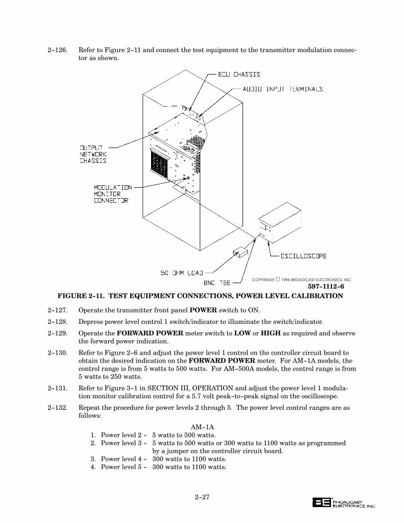
2-27
2-126. Refer to Figure 2-11 and connect the test equipment to the transmitter modulation connec�
tor as shown.
COPYRIGHT 1996 BROADCAST ELECTRONICS, INC
597-1112-6
FIGURE 2-11. TEST EQUIPMENT CONNECTIONS, POWER LEVEL CALIBRATION
2-127. Operate the transmitter front panel POWER switch to ON.
2-128. Depress power level control 1 switch/indicator to illuminate the switch/indicator.
2-129. Operate the FORWARD POWER meter switch to LOW or HIGH as required and observe
the forward power indication.
2-130. Refer to Figure 2-6 and adjust the power level 1 control on the controller circuit board to
obtain the desired indication on the FORWARD POWER meter. For AM-1A models, the
control range is from 5 watts to 500 watts. For AM-500A models, the control range is from
5 watts to 250 watts.
2-131. Refer to Figure 3-1 in SECTION III, OPERATION and adjust the power level 1 modula�
tion monitor calibration control for a 5.7 volt peak-to-peak signal on the oscilloscope.
2-132. Repeat the procedure for power levels 2 through 5. The power level control ranges are as
follows:
AM-1A
1. Power level 2 - 5 watts to 500 watts.
2. Power level 3 - 5 watts to 500 watts or 300 watts to 1100 watts as programmed
by a jumper on the controller circuit board.
3. Power level 4 - 300 watts to 1100 watts.
4. Power level 5 - 300 watts to 1100 watts.
2-28
AM-500A
1. Power level 2 - 5 watts to 250 watts.
2. Power level 3 - 5 watts to 250 watts or 150 watts to 500 watts as programmed
by a jumper on the controller circuit board.
3. Power level 4 - 150 watts to 500 watts.
4. Power level 5 - 150 watts to 500 watts.
WARNING
WARNING
DISCONNECT ALL TRANSMITTER PRIMARY POWER
BEFORE PROCEEDING.
2-133. Operate the front-panel POWER switch to OFF.
2-134. Disconnect the cable from the transmitter modulation monitor connector.
2-135. STEREO ADJUSTMENT. If the transmitter is operated in the stereo mode, the transmitter
stereo circuitry must be adjusted to compensate for antenna system variances. The pri�
mary objective in the adjustment of the transmitter is to configure the stereo circuitry to
minimize distortion and maximize separation across the entire audio band. A proof of per�
formance sheet is provided at the end of this section to record performance measurements.
To adjust the stereo circuitry, perform the following procedures and record the measure�
ments on the proof of performance sheet at the end of this section.
WARNING
WARNING
DISCONNECT ALL TRANSMITTER PRIMARY POWER
BEFORE PROCEEDING.
2-136. Operate the front-panel POWER switch to OFF.
2-137. Refer to Figure 2-12 and connect the test equipment as shown.
2-138. Operate the oscilloscope for: 1) 200 mV/div sensitivity and 2) dc coupled.
2-139. Refer to Figure 2-7 and connect an audio generator to the audio input terminals on the
ECU rear-panel.
2-140. Operate the front-panel POWER switch to ON.
2-141. Select the antenna which is configured for equalization circuit 1 operation (refer to
STEREO CIRCUIT BOARD PROGRAMMING in the preceding text if required) and deter�
mine a power level.
2-142. Depress the desired power level switch/indicator to illuminate the switch/indicator.
2-143. Refer to SECTION III, OPERATION and perform the following:
1. Operate the stereo circuit board mode control switch to illuminate the stereo
indicator. When power is applied to the transmitter, the stereo circuit board will
automatically be configured to the stereo mode.
2. Operate the stereo circuit board pilot switch to off.
3. Ensure the equalization circuit 1 indicator on the stereo circuit board is
illuminated.
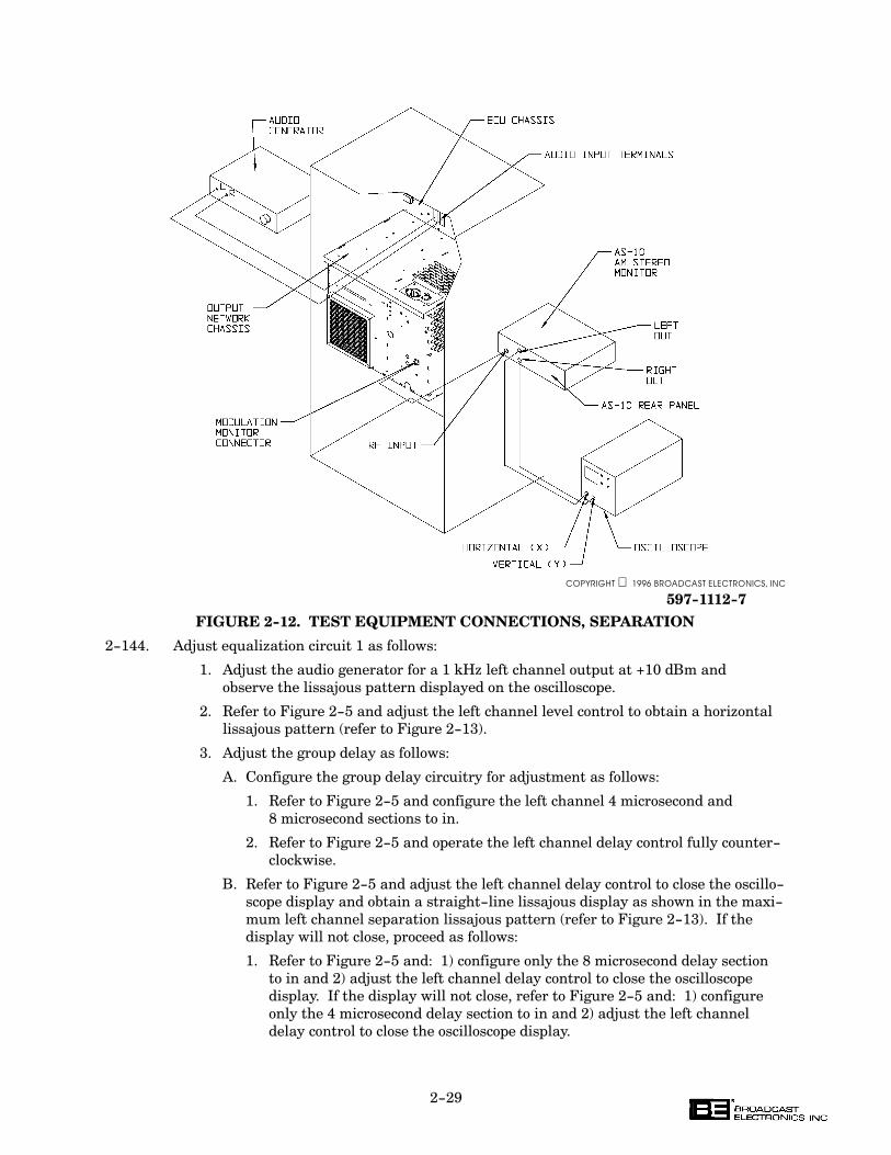
2-29
597-1112-7
FIGURE 2-12. TEST EQUIPMENT CONNECTIONS, SEPARATION
COPYRIGHT 1996 BROADCAST ELECTRONICS, INC
2-144. Adjust equalization circuit 1 as follows:
1. Adjust the audio generator for a 1 kHz left channel output at +10 dBm and
observe the lissajous pattern displayed on the oscilloscope.
2. Refer to Figure 2-5 and adjust the left channel level control to obtain a horizontal
lissajous pattern (refer to Figure 2-13).
3. Adjust the group delay as follows:
A. Configure the group delay circuitry for adjustment as follows:
1. Refer to Figure 2-5 and configure the left channel 4 microsecond and
8 microsecond sections to in.
2. Refer to Figure 2-5 and operate the left channel delay control fully counter-
clockwise.
B. Refer to Figure 2-5 and adjust the left channel delay control to close the oscillo-
scope display and obtain a straight-line lissajous display as shown in the maxi-
mum left channel separation lissajous pattern (refer to Figure 2-13). If the
display will not close, proceed as follows:
1. Refer to Figure 2-5 and: 1) configure only the 8 microsecond delay section
to in and 2) adjust the left channel delay control to close the oscilloscope
display. If the display will not close, refer to Figure 2-5 and: 1) configure
only the 4 microsecond delay section to in and 2) adjust the left channel
delay control to close the oscilloscope display.
2-30
4. Adjust the separation at 7 kHz as follows:
A. Adjust the audio generator for a 7 kHz left channel output at +10 dBm.
B. Refer to Figure 2-5 and adjust the left channel cutoff and peak controls to
obtain a maximum left channel separation lissajous pattern as shown in
Figure 2-13.
C. If a maximum left channel lissajous pattern can not be obtained, refer to Figure
2-5 and adjust the left channel delay control to close the oscilloscope display
and obtain a straight-line lissajous pattern (refer to Figure 2-13).
5. Repeat the entire procedure for the right channel. Adjust the right channel level,
cutoff, peak, and delay controls as required to obtain optimum separation and
distortion from the right channel.
6. Repeat the entire procedure for equalization circuit 2. Adjust the equalization
circuit 2 using the equalization 2 left/right channel level, cutoff, peak, delay,
controls and the equalization 2 group delay sections to obtain optimum separation
and distortion.
2-145. Once the stereo adjustment is complete: 1) refer to SECTION III, OPERATION and oper�
ate the pilot switch on the stereo circuit board to ON and 2) remove the test equipment.
2-146. SINGLE CHANNEL LEVEL. The transmitter is equipped with a single channel level con�
trol. When the transmitter is operating in the stereo mode, the level control is designed to
boost a remaining audio channel level in the event of a failure in one channel. For trans�
mitters operating in the stereo mode, adjust the single channel level control as follows:
WARNING
WARNING
DISCONNECT ALL TRANSMITTER PRIMARY POWER
BEFORE PROCEEDING.
2-147. Operate the front-panel POWER switch to OFF.
2-148. If an audio processor is used with the transmitter, ensure the processor is connected as fol�
lows:
1. Ensure normal program audio is connected to the processor input.
2. Ensure the audio processor output is connected to the transmitter audio input.
2-149. Operate the front-panel POWER switch to ON.
2-150. Depress a desired power level switch/indicator to illuminate the switch/indicator.
2-151. Refer to SECTION III, OPERATION and operate the stereo circuit board mode control
switch to illuminate the stereo indicator.
2-152. Disable one channel applied to the transmitter.
2-153. If an audio processor is used with the transmitter, refer to the audio processor manual and
adjust the processor single channel limiter as described in the procedure.
2-154. Refer to SECTION III, OPERATION and operate the stereo circuit board mode control
switch to illuminate the mono left or mono right indicator as determined by the remaining
operating audio channel applied to the transmitter.
2-155. Refer to Figure 2-4 and adjust the single channel level control on the exciter circuit board
as required to obtain an approximate 100% modulation indication on the modulation moni�
tor.

597-0095-19
FIGURE 2-13. EQUALIZATION LISSAJOUS PATTERNS(2-31/2-32)
COPYRIGHT 1996 BROADCAST ELECTRONICS, INC

3-1
SECTION III
OPERATION
3-1. INTRODUCTION.
3-2. This section identifies all controls and indicators associated with the AM-1A/AM-500A
transmitters and provides standard operating procedures.
3-3. CONTROLS AND INDICATORS.
3-4. Figures 3-1 through 3-3 present the location of all controls and indicators associated with
normal operation of the AM-1A/AM-500A transmitters. Tables 3-1 through 3-3 present
the functions of each control or indicator. Refer to Figures 3-1 through 3-3 and Tables 3-1
through 3-3 for a description of the controls and indicators associated with the transmit�
ter.
TABLE 3-1. AM-1A/AM-500A CONTROLS AND INDICATORS
(Sheet 1 of 2)
INDEX
NO. NOMENCLATURE FUNCTION
1 FORWARD POWER Displays the transmitter forward power output in
Meter watts as selected by the FORWARD POWER Meter
LOW/HIGH/OFF switch.
2 FORWARD POWER Configures the FORWARD POWER meter: 1) to
Meter HIGH/LOW/OFF display forward power information on the HIGH
Switch scale, 2) to display forward power information on the
LOW scale, or 3) to off. In the AM-1A, the HIGH scale is
from 0 to 1200 watts and 2) LOW scale is from 0 to 300
watts. In the AM-500A, the HIGH scale is from 0 to 600
watts and 2) LOW scale is from 0 to 150 watts.
3 REFLECTED POWER Displays the transmitter reflected power output in
Meter watts or the ac input voltage in volts as selected by
the REFLECTED POWER HIGH/LOW/VAC
Switch.
4 REFLECTED POWER Configures the REFLECTED POWER Meter to
Meter HIGH/LOW/VAC display: 1) reflected power information on the HIGH
Switch scale, 2) reflected power information on the LOW
scale, or 3) the ac input voltage. In the AM-1A, the HIGH
scale is from 0 to 120 watts and 2) LOW scale is from 0 to 30
watts. The ac volts scale is from 150 to 300 volts. In the
AM-500A, The HIGH scale is from 0 to 60 watts and 2) LOW
scale is from 0 to 12 watts. The ac volts scale is from 150 to
300 volts.
5 POWER Controls the application of ac power to the transmitter.
Switch
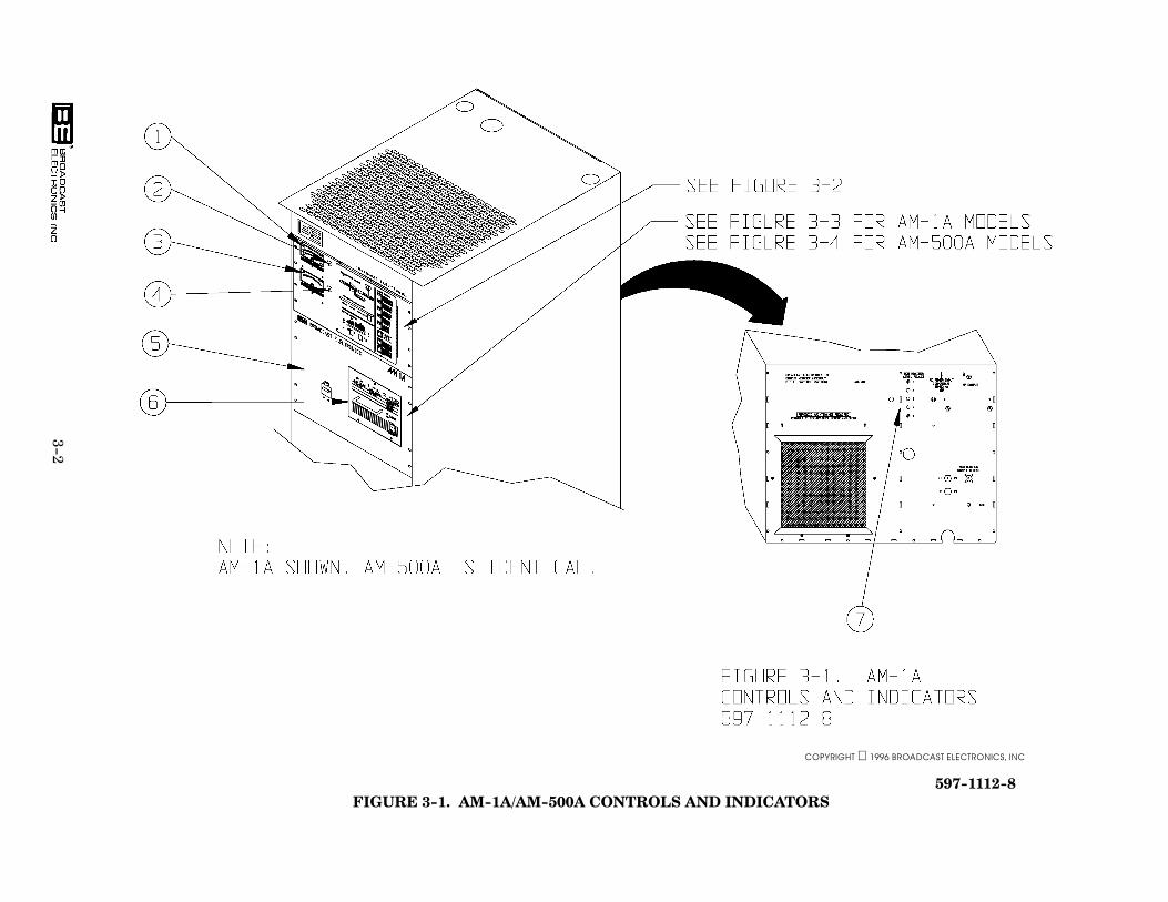
3-2
597-1112-8
COPYRIGHT 1996 BROADCAST ELECTRONICS, INC
FIGURE 3-1. AM-1A/AM-500A CONTROLS AND INDICATORS
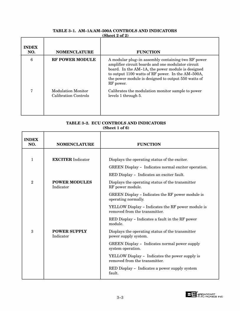
3-3
TABLE 3-1. AM-1A/AM-500A CONTROLS AND INDICATORS
(Sheet 2 of 2)
INDEX
NO. NOMENCLATURE FUNCTION
6 RF POWER MODULE A modular plug-in assembly containing two RF power
amplifier circuit boards and one modulator circuit
board. In the AM-1A, the power module is designed
to output 1100 watts of RF power. In the AM-500A,
the power module is designed to output 550 watts of
RF power.
7 Modulation Monitor Calibrates the modulation monitor sample to power
Calibration Controls levels 1 through 5.
TABLE 3-2. ECU CONTROLS AND INDICATORS
(Sheet 1 of 6)
INDEX
NO. NOMENCLATURE FUNCTION
1 EXCITER Indicator Displays the operating status of the exciter.
GREEN Display - Indicates normal exciter operation.
RED Display - Indicates an exciter fault.
2 POWER MODULES Displays the operating status of the transmitter
Indicator RF power module.
GREEN Display - Indicates the RF power module is
operating normally.
YELLOW Display - Indicates the RF power module is
removed from the transmitter.
RED Display - Indicates a fault in the RF power
module.
3 POWER SUPPLY Displays the operating status of the transmitter
Indicator power supply system.
GREEN Display - Indicates normal power supply
system operation.
YELLOW Display - Indicates the power supply is
removed from the transmitter.
RED Display - Indicates a power supply system
fault.
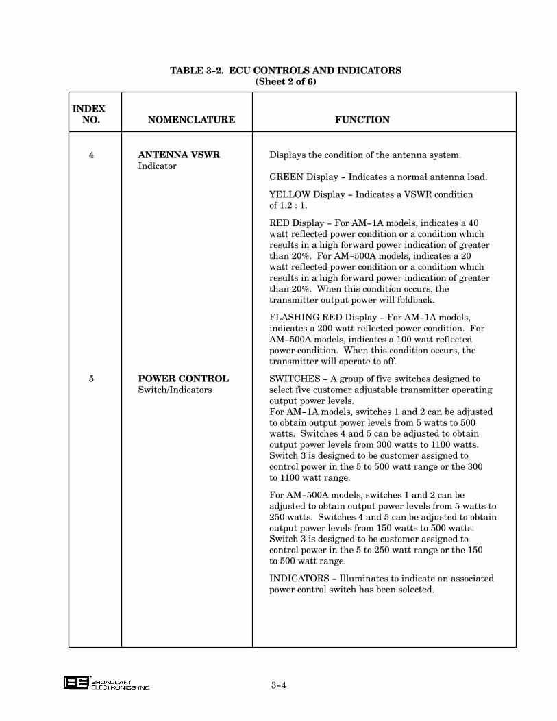
3-4
TABLE 3-2. ECU CONTROLS AND INDICATORS
(Sheet 2 of 6)
INDEX
NO. NOMENCLATURE FUNCTION
4 ANTENNA VSWR Displays the condition of the antenna system.
Indicator
GREEN Display - Indicates a normal antenna load.
YELLOW Display - Indicates a VSWR condition
of 1.2 : 1.
RED Display - For AM-1A models, indicates a 40
watt reflected power condition or a condition which
results in a high forward power indication of greater
than 20%. For AM-500A models, indicates a 20
watt reflected power condition or a condition which
results in a high forward power indication of greater
than 20%. When this condition occurs, the
transmitter output power will foldback.
FLASHING RED Display - For AM-1A models,
indicates a 200 watt reflected power condition. For
AM-500A models, indicates a 100 watt reflected
power condition. When this condition occurs, the
transmitter will operate to off.
5 POWER CONTROL SWITCHES - A group of five switches designed to
Switch/Indicators select five customer adjustable transmitter operating
output power levels.
For AM-1A models, switches 1 and 2 can be adjusted
to obtain output power levels from 5 watts to 500
watts. Switches 4 and 5 can be adjusted to obtain
output power levels from 300 watts to 1100 watts.
Switch 3 is designed to be customer assigned to
control power in the 5 to 500 watt range or the 300
to 1100 watt range.
For AM-500A models, switches 1 and 2 can be
adjusted to obtain output power levels from 5 watts to
250 watts. Switches 4 and 5 can be adjusted to obtain
output power levels from 150 watts to 500 watts.
Switch 3 is designed to be customer assigned to
control power in the 5 to 250 watt range or the 150
to 500 watt range.
INDICATORS - Illuminates to indicate an associated
power control switch has been selected.
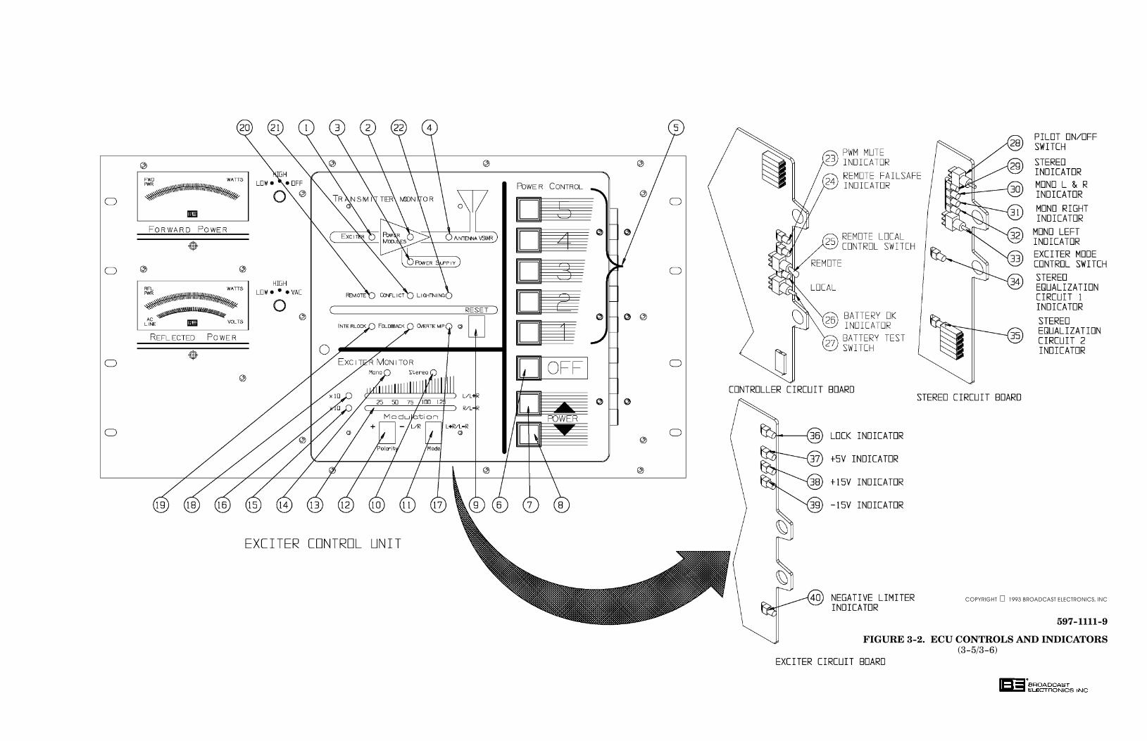
597-1111-9
FIGURE 3-2. ECU CONTROLS AND INDICATORS(3-5/3-6)
COPYRIGHT 1993 BROADCAST ELECTRONICS, INC
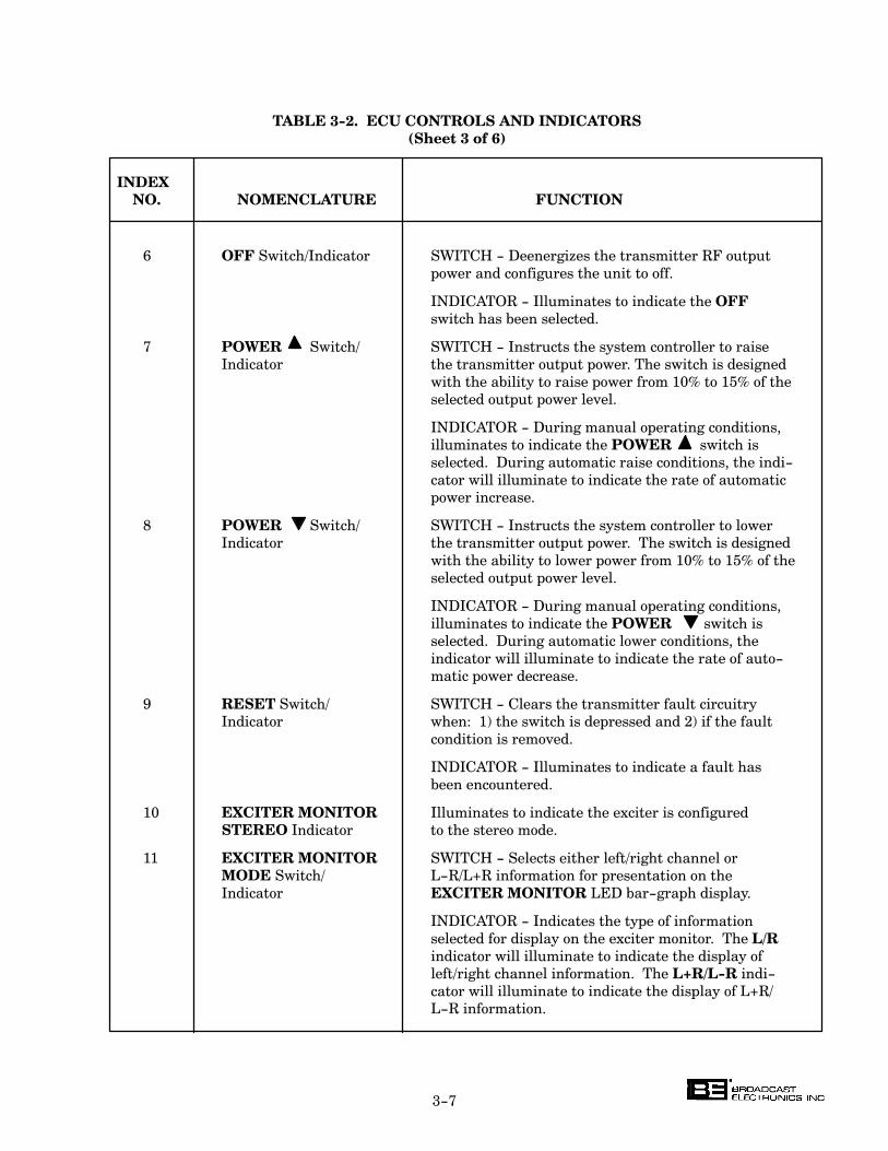
3-7
TABLE 3-2. ECU CONTROLS AND INDICATORS
(Sheet 3 of 6)
INDEX
NO. NOMENCLATURE FUNCTION
6 OFF Switch/Indicator SWITCH - Deenergizes the transmitter RF output
power and configures the unit to off.
INDICATOR - Illuminates to indicate the OFF
switch has been selected.
7 POWER Switch/ SWITCH - Instructs the system controller to raise
Indicator the transmitter output power. The switch is designed
with the ability to raise power from 10% to 15% of the
selected output power level.
INDICATOR - During manual operating conditions,
illuminates to indicate the POWER switch is
selected. During automatic raise conditions, the indi-
cator will illuminate to indicate the rate of automatic
power increase.
8 POWER Switch/ SWITCH - Instructs the system controller to lower
Indicator the transmitter output power. The switch is designed
with the ability to lower power from 10% to 15% of the
selected output power level.
INDICATOR - During manual operating conditions,
illuminates to indicate the POWER switch is
selected. During automatic lower conditions, the
indicator will illuminate to indicate the rate of auto-
matic power decrease.
9 RESET Switch/ SWITCH - Clears the transmitter fault circuitry
Indicator when: 1) the switch is depressed and 2) if the fault
condition is removed.
INDICATOR - Illuminates to indicate a fault has
been encountered.
10 EXCITER MONITOR Illuminates to indicate the exciter is configured
STEREO Indicator to the stereo mode.
11 EXCITER MONITOR SWITCH - Selects either left/right channel or
MODE Switch/ L-R/L+R information for presentation on the
Indicator EXCITER MONITOR LED bar-graph display.
INDICATOR - Indicates the type of information
selected for display on the exciter monitor. The L/R
indicator will illuminate to indicate the display of
left/right channel information. The L+R/L-R indi-
cator will illuminate to indicate the display of L+R/
L-R information.
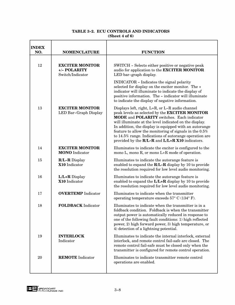
3-8
TABLE 3-2. ECU CONTROLS AND INDICATORS
(Sheet 4 of 6)
INDEX
NO. NOMENCLATURE FUNCTION
12 EXCITER MONITOR SWITCH - Selects either positive or negative peak
+/- POLARITY audio for application to the EXCITER MONITOR
Switch/Indicator LED bar-graph display.
INDICATOR - Indicates the signal polarity
selected for display on the exciter monitor. The +
indicator will illuminate to indicate the display of
positive information. The - indicator will illuminate
to indicate the display of negative information.
13 EXCITER MONITOR Displays left, right, L+R, or L-R audio channel
LED Bar-Graph Display peak levels as selected by the EXCITER MONITOR
MODE and POLARITY switches. Each indicator
will illuminate at the level indicated on the display.
In addition, the display is equipped with an autorange
feature to allow the monitoring of signals in the 0.5%
to 14.5% range. Indications of autorange operation are
provided by the R/L-R and L/L+R X10 indicators.
14 EXCITER MONITOR Illuminates to indicate the exciter is configured to the
MONO Indicator mono L, mono R, or mono L+R mode of operation.
15 R/L-R Display Illuminates to indicate the autorange feature is
X10 Indicator enabled to expand the R/L-R display by 10 to provide
the resolution required for low level audio monitoring.
16 L/L+R Display Illuminates to indicate the autorange feature is
X10 Indicator enabled to expand the L/L+R display by 10 to provide
the resolution required for low level audio monitoring.
17 OVERTEMP Indicator Illuminates to indicate when the transmitter
operating temperature exceeds 57° C (134° F).
18 FOLDBACK Indicator Illuminates to indicate when the transmitter is in a
foldback condition. Foldback is when the transmitter
output power is automatically reduced in response to
one of the following fault conditions: 1) high reflected
power, 2) high forward power, 3) high temperature, or
4) detection of a lightning potential.
19 INTERLOCK Illuminates to indicate the internal interlock, external
Indicator interlock, and remote control fail�safe are closed. The
remote control fail�safe must be closed only when the
transmitter is configured for remote control operation.
20 REMOTE Indicator Illuminates to indicate transmitter remote control
operations are enabled.
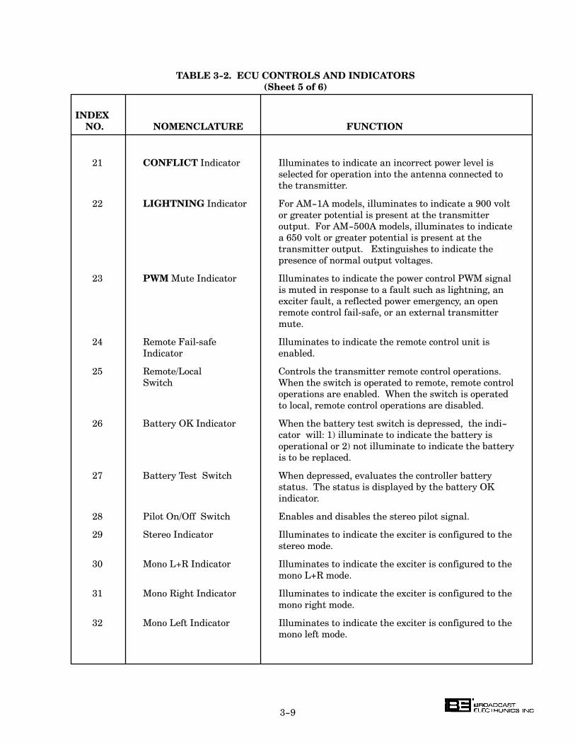
3-9
TABLE 3-2. ECU CONTROLS AND INDICATORS
(Sheet 5 of 6)
INDEX
NO. NOMENCLATURE FUNCTION
21 CONFLICT Indicator Illuminates to indicate an incorrect power level is
selected for operation into the antenna connected to
the transmitter.
22 LIGHTNING Indicator For AM-1A models, illuminates to indicate a 900 volt
or greater potential is present at the transmitter
output. For AM-500A models, illuminates to indicate
a 650 volt or greater potential is present at the
transmitter output. Extinguishes to indicate the
presence of normal output voltages.
23 PWM Mute Indicator Illuminates to indicate the power control PWM signal
is muted in response to a fault such as lightning, an
exciter fault, a reflected power emergency, an open
remote control fail�safe, or an external transmitter
mute.
24 Remote Fail�safe Illuminates to indicate the remote control unit is
Indicator enabled.
25 Remote/Local Controls the transmitter remote control operations.
Switch When the switch is operated to remote, remote control
operations are enabled. When the switch is operated
to local, remote control operations are disabled.
26 Battery OK Indicator When the battery test switch is depressed, the indi-
cator will: 1) illuminate to indicate the battery is
operational or 2) not illuminate to indicate the battery
is to be replaced.
27 Battery Test Switch When depressed, evaluates the controller battery
status. The status is displayed by the battery OK
indicator.
28 Pilot On/Off Switch Enables and disables the stereo pilot signal.
29 Stereo Indicator Illuminates to indicate the exciter is configured to the
stereo mode.
30 Mono L+R Indicator Illuminates to indicate the exciter is configured to the
mono L+R mode.
31 Mono Right Indicator Illuminates to indicate the exciter is configured to the
mono right mode.
32 Mono Left Indicator Illuminates to indicate the exciter is configured to the
mono left mode.
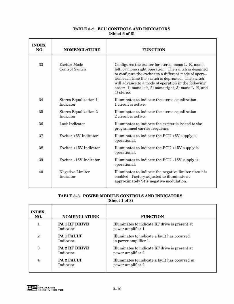
3-10
TABLE 3-2. ECU CONTROLS AND INDICATORS
(Sheet 6 of 6)
INDEX
NO. NOMENCLATURE FUNCTION
33 Exciter Mode Configures the exciter for stereo, mono L+R, mono
Control Switch left, or mono right operation. The switch is designed
to configure the exciter to a different mode of opera-
tion each time the switch is depressed. The switch
will advance to a mode of operation in the following
order: 1) mono left, 2) mono right, 3) mono L+R, and
4) stereo.
34 Stereo Equalization 1 Illuminates to indicate the stereo equalization
Indicator 1 circuit is active.
35 Stereo Equalization 2 Illuminates to indicate the stereo equalization
Indicator 2 circuit is active.
36 Lock Indicator Illuminates to indicate the exciter is locked to the
programmed carrier frequency.
37 Exciter +5V Indicator Illuminates to indicate the ECU +5V supply is
operational.
38 Exciter +15V Indicator Illuminates to indicate the ECU +15V supply is
operational.
39 Exciter -15V Indicator Illuminates to indicate the ECU -15V supply is
operational.
40 Negative Limiter Illuminates to indicate the negative limiter circuit is
Indicator enabled. Factory adjusted to illuminate at
approximately 94% negative modulation.
TABLE 3-3. POWER MODULE CONTROLS AND INDICATORS
(Sheet 1 of 3)
INDEX
NO. NOMENCLATURE FUNCTION
1 PA 1 RF DRIVE Illuminates to indicate RF drive is present at
Indicator power amplifier 1.
2 PA 1 FAULT Illuminates to indicate a fault has occurred
Indicator in power amplifier 1.
3 PA 2 RF DRIVE Illuminates to indicate RF drive is present at
Indicator power amplifier 2.
4 PA 2 FAULT Illuminates to indicate a fault has occurred in
Indicator power amplifier 2.
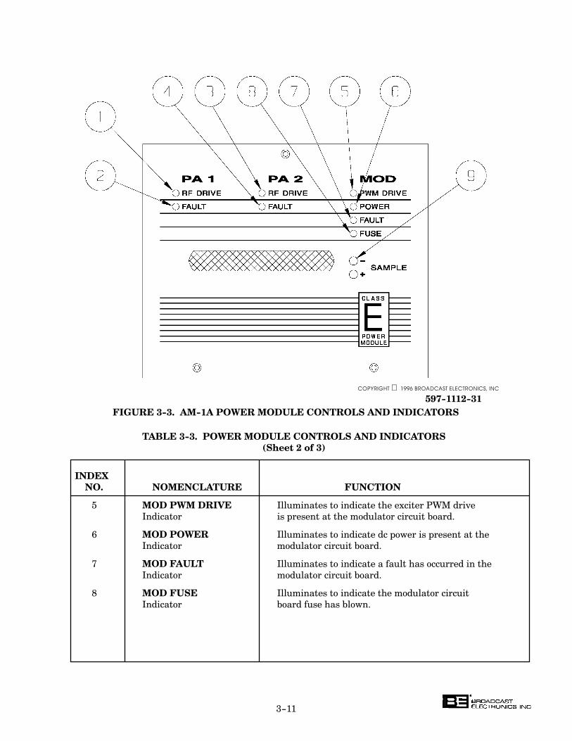
3-11
FIGURE 3-3. AM-1A POWER MODULE CONTROLS AND INDICATORS
597-1112-31
COPYRIGHT 1996 BROADCAST ELECTRONICS, INC
TABLE 3-3. POWER MODULE CONTROLS AND INDICATORS
(Sheet 2 of 3)
INDEX
NO. NOMENCLATURE FUNCTION
5 MOD PWM DRIVE Illuminates to indicate the exciter PWM drive
Indicator is present at the modulator circuit board.
6 MOD POWER Illuminates to indicate dc power is present at the
Indicator modulator circuit board.
7 MOD FAULT Illuminates to indicate a fault has occurred in the
Indicator modulator circuit board.
8 MOD FUSE Illuminates to indicate the modulator circuit
Indicator board fuse has blown.

3-12
TABLE 3-3. POWER MODULE CONTROLS AND INDICATORS
(Sheet 3 of 3)
INDEX
NO. NOMENCLATURE FUNCTION
9 MOD SAMPLE Provides a dc voltage sample of the modulator circuit
board output. For AM-1A models, the sample will be
equal to approximately 6 volts dc at 1100 watts. For
AM-500A models, the sample will be equal to
approximately 4.2 volts dc at 500 watts. Refer to the
factory test data sheets for the exact value.
3-5. OPERATION.
NOTE
NOTE
ENSURE THE TRANSMITTER IS COMPLETELY IN�
STALLED PRIOR TO PERFORMING THE FOLLOWING
PROCEDURES.
3-6. TURN-ON.
3-7. OPERATION. Operate the transmitter to ON by performing the following procedure.
3-8. Ensure the front-panel POWER switch is operated to ON. The ECU and RF power mod�
ule indicators will illuminate.
3-9. Observe the ECU and RF power module indicators. Ensure normal operating conditions
are displayed by all indicators. If an indicator displays a fault condition, operate the ac
power switch to off and locate the problem.
3-10. Select an output power level by depressing the desired power level switch/indicator. The
following events will occur:
1. The power level switch indicator will illuminate.
2. The transmitter flushing fan will begin operation.
3. The transmitter output power will be displayed on the FORWARD and
REFLECTED power meters.
3-11. Operate the FORWARD and REFLECTED power meters by performing the METERING
procedures in the following text to observe the transmitter forward and reflected power
indications.
3-12. Adjust the transmitter output power if required by performing the POWER ADJUST pro�
cedure presented in the following text.
3-13. If remote control operation is desired, operate the local/remote switch on the controller cir�
cuit board to remote. This will enable both local and remote operation.
3-14. TURN OFF.
3-15. Operate the transmitter to OFF by depressing the OFF switch/indicator to illuminate the
switch/indicator. The transmitter will operate to off.
3-13
3-16. METERING.
3-17. FORWARD POWER. The forward power meter presents forward power indications. To
operate the meter, proceed as follows:
1. To monitor low forward power levels, operate the FORWARD POWER meter
switch to LOW. For AM-1A models, the LOW scale is from 0 to 300 watts. For
AM-500A models, the LOW scale is from 0 to 150 watts.
2. To monitor high forward power levels, operate the FORWARD POWER meter
switch to HIGH. For AM-1A models, the HIGH scale is from 0 to 1200 watts. For
AM-500A models, the HIGH scale is from 0 to 600 watts.
3. To configure the FORWARD POWER meter to off, operate the FORWARD
POWER meter switch to OFF.
3-18. REFLECTED POWER. The reflected power meter presents reflected power and ac input
indications. To operate the meter, proceed as follows:
1. To monitor low reflected power levels, operate the REFLECTED POWER meter
switch to LOW. For AM-1A models, the LOW scale is from 0 to 30 watts. For
AM-500A models, the LOW scale is from 0 to 12 watts.
2. To monitor high reflected power levels, operate the REFLECTED POWER meter
switch to HIGH. For AM-1A models, the HIGH scale is from 0 to 120 watts. For
AM-500A models, the HIGH scale is from 0 to 60 watts.
3. To monitor the ac input voltage, operate the REFLECTED POWER meter
switch to VAC.
3-19. POWER ADJUST.
3-20. The POWER and switches adjust the transmitter output power. To adjust the trans�
mitter power, proceed as follows:
1. Depress the POWER switch to increase the transmitter output power. Observe
the transmitter output power indications on the FORWARD and REFLECTED
power meters.
The switch will increase power from 10% to 15% of the selected power level.
OR
2. Depress the POWER switch to decrease the transmitter output power. Observe
the transmitter output power indications on the FORWARD and REFLECTED
power meters.
The switch will decrease power from 10% to 15% of the selected power level.
3-21. MONO/STEREO OPERATION.
3-22. To configure the transmitter for monophonic or stereophonic operation, perform the follow�
ing procedures.
3-23. STEREO OPERATION. To configure the transmitter for stereo operations, depress the ex�
citer mode control switch to illuminate the stereo indicator on the stereo circuit board. In
addition, the ECU front-panel stereo indicator will illuminate.
3-24. MONO OPERATION. The transmitter can be configured to the monophonic mode by:
1) manually selecting the desired mono mode using the stereo circuit board or 2) automati�
cally configuring the transmitter by removing the stereo circuit board. To configure the
transmitter for mono operations, proceed as follows:

3-14
3-25. Mono Operation - Stereo Circuit Board. To configure the transmitter for mono operationusing the stereo circuit board, depress the exciter mode control switch to illuminate themono L+R, mono left, or mono right indicators on the stereo circuit board. In addition, theECU front-panel MONO indicator will illuminate.
3-26. Mono Operation - No Stereo Circuit Board. In the event of a stereo circuit board failure,the transmitter will automatically configure to the monophonic mode when the stereo cir�cuit board is removed from the ECU. To remove the stereo circuit board and configure thetransmitter for monophonic operation, proceed as follows:
CAUTION
CAUTION
TO PREVENT DAMAGE TO THE TRANSMITTER, EN�
SURE THE TRANSMITTER PRIMARY POWER IS OPER�
ATED TO OFF BEFORE REMOVING THE STEREO CIR�
CUIT BOARD.
1. Operate the transmitter primary power to off.
2. Completely remove the stereo circuit board from the ECU. Do not leave the circuit
board in the ECU chassis.
3. Refer to Figure 2-5 in SECTION II, INSTALLATION and ensure the monophonic
audio channel select jumper is configured for the desired audio channel.
4. If required, adjust the single channel level by referring to SECTION II, INSTAL-
LATION and performing the SINGLE CHANNEL LEVEL procedure.
3-27. PILOT CONTROL.
3-28. The pilot switch on the stereo circuit board controls the pilot tone. Operate the pilot switch
to on to enable the pilot tone. Operate the pilot switch to off to disable the pilot tone.
3-29. EXCITER MONITOR OPERATION.
3-30. The following text presents procedures for specific exciter monitoring functions. Perform
the appropriate procedure for the type of monitor function desired.
3-31. MONO/STEREO INDICATIONS. The MONO and STEREO indicators display the oper�
ating mode of the exciter. The MONO indicator will illuminate to indicate when the ex�
citer is configured for mono L+R, mono left, or mono right operation. The STEREO indica�
tor will illuminate to indicate when the exciter is configured for stereo operation.
3-32. INPUT SELECTION. Depress the L/R/L+R/L-R MODE switch/indicator to: 1) illuminate
the L/R indicator to select left and right channel information or 2) illuminate the L+R/L-R
indicator to select L+R and L-R information. The selected parameter will appear on the
EXCITER MONITOR display.
3-33. POLARITY SELECTION. Depress the POLARITY switch/indicator to: 1) illuminate the +
indicator to select positive peak audio or 2) illuminate the - indicator to select negative
peak audio. The selected parameter will appear on the EXCITER MONITOR display.
3-34. X10 AUTORANGE INDICATIONS. The EXCITER MONITOR display is designed with
an autorange function to provide the appropriate resolution for the applied signal level.
The L/L+R display X10 indicator will illuminate to indicate the display is expanded by 10.
The R/L-R display X10 indicator will illuminate to indicate the display is expanded by 10.

3-15
3-35. FAULT RESET.
3-36. The transmitter monitors several parameters for fault conditions. The RESET indicator
will illuminate to indicate a fault when one of the following conditions occur:
1) over-temperature, 2) exciter fault, 3) power supply fault, 4) RF power module fault,
5) high reflected/forward power, 6) reflected power emergency, or 7) lightning. If a power
supply fault is encountered, the transmitter ac power must be disconnected to remove the
fault condition (refer to POWER SUPPLY FAULT RESET in the following text). Once
the fault condition is removed, the fault circuitry must be reset. To reset the fault circuitry,
depress the RESET switch. The fault circuitry will be reset.
3-37. POWER SUPPLY FAULT RESET.
3-38. If a power supply fault is encountered, ac power must be disconnected from the transmitter
to clear the fault. To reset a power supply fault, proceed as follows:
1. Operate the front-panel POWER switch to OFF.
2. Operate the front-panel POWER switch to ON.
3. Depress the RESET switch.
3-39. OVER-CYCLE OFF.
3-40. The transmitter controller is equipped with an on/off cycle counter circuit. The circuit is
designed to monitor transmitter on/off cycles. If the transmitter is operated on/off seven
times within 15 seconds, the transmitter will automatically operate to OFF. The power
level or OFF switch/indicators will not respond. To operate the transmitter to ON, proceed
as follows:
1. Do not depress any power level switch/indicators or the OFF switch/indicator for
approximately 30 seconds. This allows the circuit to reset.
2. Depress the desired power level switch/indicator.
3-41. OVER-MODULATION PWM MUTE.
3-42. The transmitter is protected from modulation levels above 150% by an over-modulation
circuit. If the transmitter modulation increases to a level above 150%, the PWM signal
will be muted. This will mute the output power and prevent damage to the transmitter
power supply modules.
3-43. TRANSMITTER MONITOR.
3-44. The TRANSMITTER MONITOR is designed to present the operating status of: 1) the
exciter, 2) the RF power module, 3) the power supply, 4) the antenna, 5) the remote control,
6) antenna conflict conditions, 7) lightning conditions, 8) interlocks, 9) foldback conditions,
and 10) over-temperature conditions. Use the information presented in Table 3-2 to deter�
mine the status of the transmitter components and operating conditions.
3-45. BATTERY TEST.
3-46. The battery test and battery OK indicator check the ECU battery backup system. To check
the ECU battery, depress the battery test switch. The battery OK indicator will illuminate
to indicate an acceptable battery voltage. If the battery OK indicator does not illuminate,
replace the battery.
3-47. CONTROLLER PWM MUTE INDICATOR.
3-48. The PWM mute indicator illuminates to indicate when the power control PWM signal is
muted. The power control PWM signal is muted during: 1) lightning conditions, 2) an ex�
citer fault, 3) reflected power emergency conditions, 4) an open remote control fail�safe, or
5) a transmitter mute control signal.
3-16
3-49. CONTROLLER REMOTE FAILSAFE INDICATOR.
3-50. The controller remote fail�safe indicator illuminates to indicate the remote control unit is
enabled. The indicator will extinguish when the remote control unit is disabled.
3-51. EXCITER LOCK INDICATOR.
3-52. The exciter circuit board lock indicator illuminates to indicate when the exciter is locked to
the programmed carrier frequency. The indicator will extinguish when the exciter is un�
locked from the programmed carrier frequency.
3-53. EXCITER +5V/+15V/-15V INDICATORS.
3-54. The exciter circuit board +5V, +15V, and -15V indicators display the status of the operat�
ing potentials from the ECU power supply. The +5V, +15V, and -15V indicators will illu�
minate to indicate the +5 volt, +15 volt, and -15 volt supplies are operational.
3-55. STEREO EQUALIZATION INDICATORS.
3-56. The stereo circuit board equalization 1 indicator illuminates to indicate when equalization
circuit 1 is selected. The stereo circuit board equalization 2 indicator illuminates to indi�
cate when equalization circuit 2 is selected.
3-57. RF POWER MODULE INDICATORS.
3-58. The RF power module indicators are designed to present the operating status of the power
amplifier circuit boards and the modulator circuit board. Use the information presented in
Table 3-3 to determine the status of the power amplifier circuit board(s) and the modulator
circuit board.
3-59. HIGH AC LINE CONDITIONS.
3-60. The transmitter is equipped with a feature to mute the transmitter output power in the
event the ac power line increases above 270 volts. If this occurs: 1) the transmitter output
power will be muted and 2) no fault or emergency condition will be generated by the trans�
mitter. The transmitter will unmute when the high ac line condition is removed.
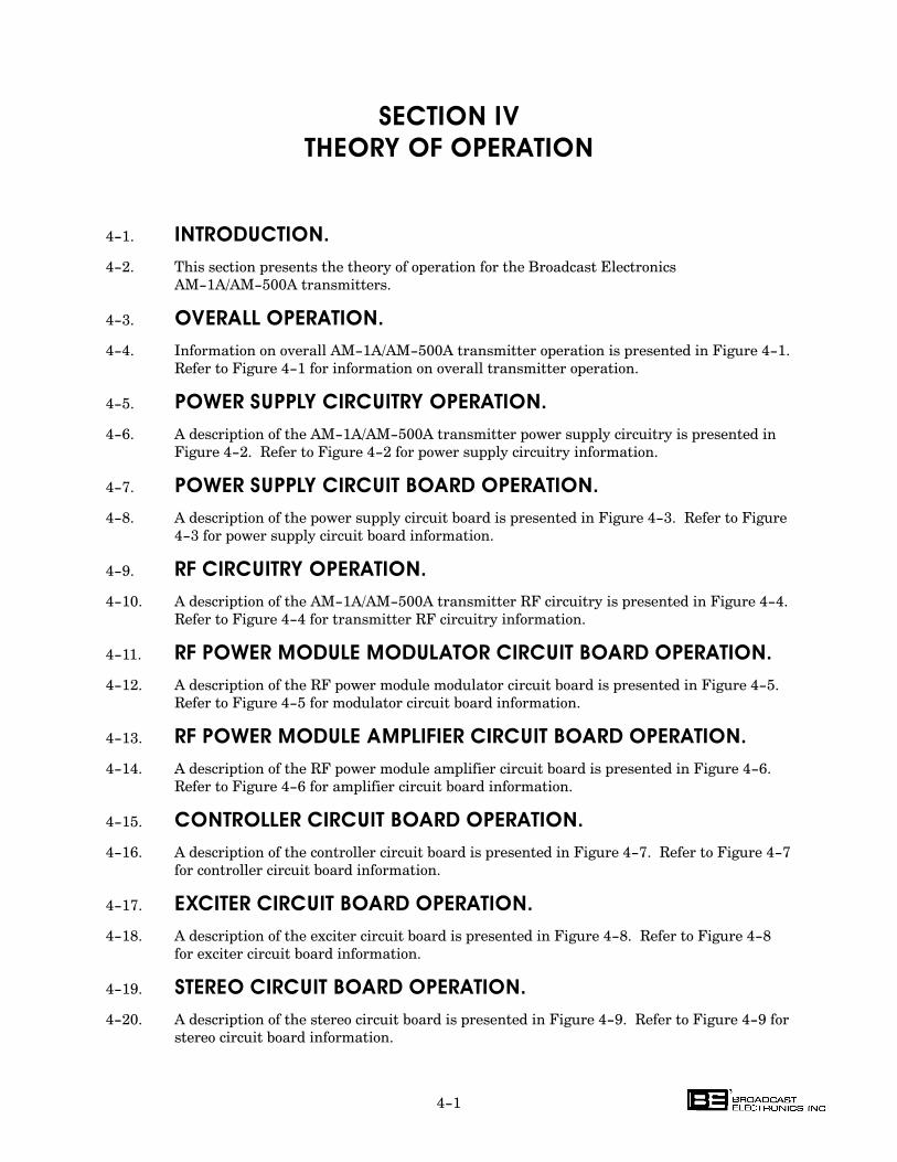
4-1
SECTION IV
THEORY OF OPERATION
4-1. INTRODUCTION.
4-2. This section presents the theory of operation for the Broadcast Electronics
AM-1A/AM-500A transmitters.
4-3. OVERALL OPERATION.
4-4. Information on overall AM-1A/AM-500A transmitter operation is presented in Figure 4-1.
Refer to Figure 4-1 for information on overall transmitter operation.
4-5. POWER SUPPLY CIRCUITRY OPERATION.
4-6. A description of the AM-1A/AM-500A transmitter power supply circuitry is presented in
Figure 4-2. Refer to Figure 4-2 for power supply circuitry information.
4-7. POWER SUPPLY CIRCUIT BOARD OPERATION.
4-8. A description of the power supply circuit board is presented in Figure 4-3. Refer to Figure
4-3 for power supply circuit board information.
4-9. RF CIRCUITRY OPERATION.
4-10. A description of the AM-1A/AM-500A transmitter RF circuitry is presented in Figure 4-4.
Refer to Figure 4-4 for transmitter RF circuitry information.
4-11. RF POWER MODULE MODULATOR CIRCUIT BOARD OPERATION.
4-12. A description of the RF power module modulator circuit board is presented in Figure 4-5.
Refer to Figure 4-5 for modulator circuit board information.
4-13. RF POWER MODULE AMPLIFIER CIRCUIT BOARD OPERATION.
4-14. A description of the RF power module amplifier circuit board is presented in Figure 4-6.
Refer to Figure 4-6 for amplifier circuit board information.
4-15. CONTROLLER CIRCUIT BOARD OPERATION.
4-16. A description of the controller circuit board is presented in Figure 4-7. Refer to Figure 4-7
for controller circuit board information.
4-17. EXCITER CIRCUIT BOARD OPERATION.
4-18. A description of the exciter circuit board is presented in Figure 4-8. Refer to Figure 4-8
for exciter circuit board information.
4-19. STEREO CIRCUIT BOARD OPERATION.
4-20. A description of the stereo circuit board is presented in Figure 4-9. Refer to Figure 4-9 for
stereo circuit board information.

4-2
BLANK PAGE
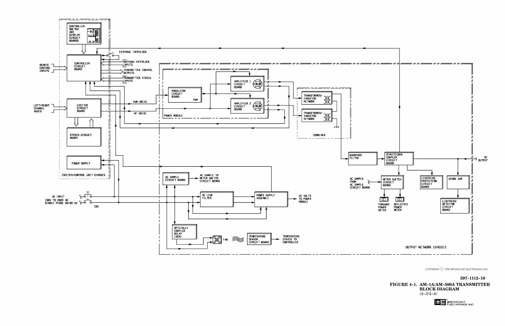
597-1112-10
FIGURE 4-1. AM-1A/AM-500A TRANSMITTER BLOCK DIAGRAM(4-3/4-4)
COPYRIGHT 1996 BROADCAST ELECTRONICS, INC
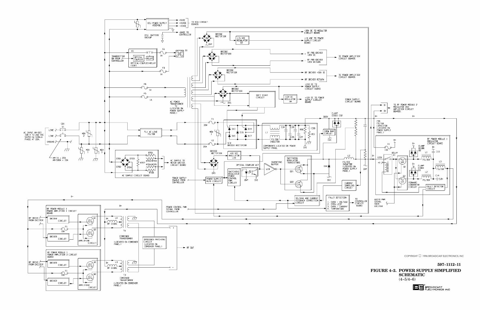
597-1112-11
FIGURE 4-2. POWER SUPPLY SIMPLIFIED SCHEMATIC(4-5/4-6)
COPYRIGHT 1996 BROADCAST ELECTRONICS, INC
597-1112-28A
FIGURE 1-1. POWER SUPPLY CIRCUIT BOARD SIMPLIFIED SCHEMATIC(4-7/4-8)
COPYRIGHT 1997 BROADCAST ELECTRONICS, INC

D6
597-1112-12
FIGURE 4-4. RF CIRCUITRY SIMPLIFIED SCHEMATIC(4-9/4-10)
COPYRIGHT 1996 BROADCAST ELECTRONICS, INC
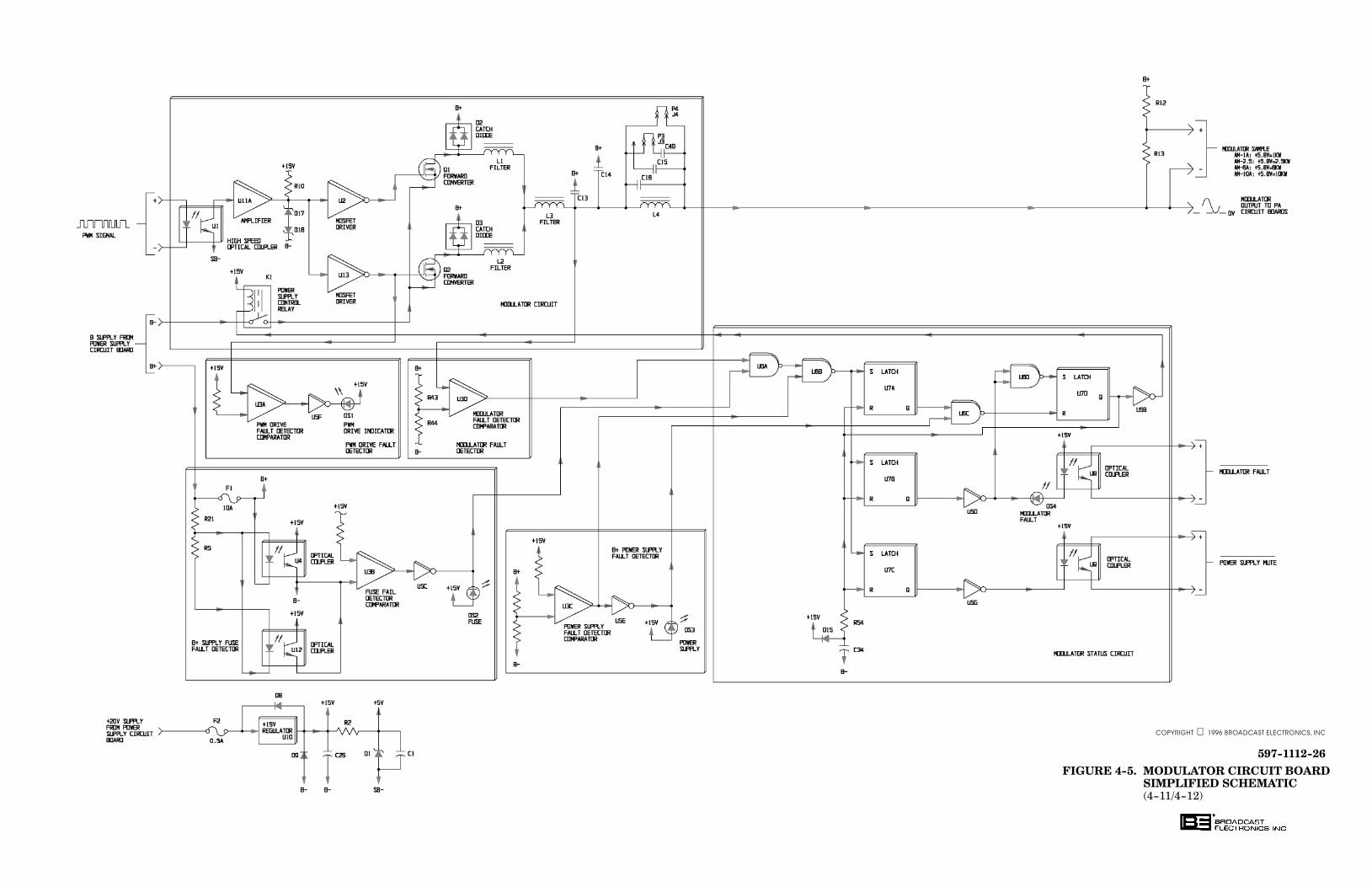
597-1112-26
FIGURE 4-5. MODULATOR CIRCUIT BOARD SIMPLIFIED SCHEMATIC(4-11/4-12)
COPYRIGHT 1996 BROADCAST ELECTRONICS, INC

597-1112-27
FIGURE 4-6. POWER AMPLIFIER CIRCUIT BOARDSIMPLIFIED SCHEMATIC(4-13/4-14)
COPYRIGHT 1996 BROADCAST ELECTRONICS, INC

597-1112-29
FIGURE 4-7. CONTROLLER CIRCUIT BOARD SIMPLIFIED SCHEMATIC(SHEET 1 OF 2)(4-15/4-16)
COPYRIGHT 1996 BROADCAST ELECTRONICS, INC
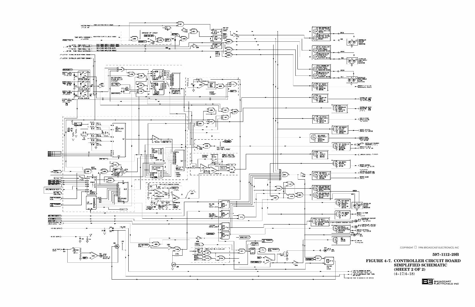
597-1112-29B
FIGURE 4-7. CONTROLLER CIRCUIT BOARD SIMPLIFIED SCHEMATIC(SHEET 2 OF 2)(4-17/4-18)
COPYRIGHT 1996 BROADCAST ELECTRONICS, INC

597-1112-24A
FIGURE 4-8. EXCITER CIRCUIT BOARD SIMPLIFIED SCHEMATIC(4-19/4-20)
COPYRIGHT 1996 BROADCAST ELECTRONICS, INC
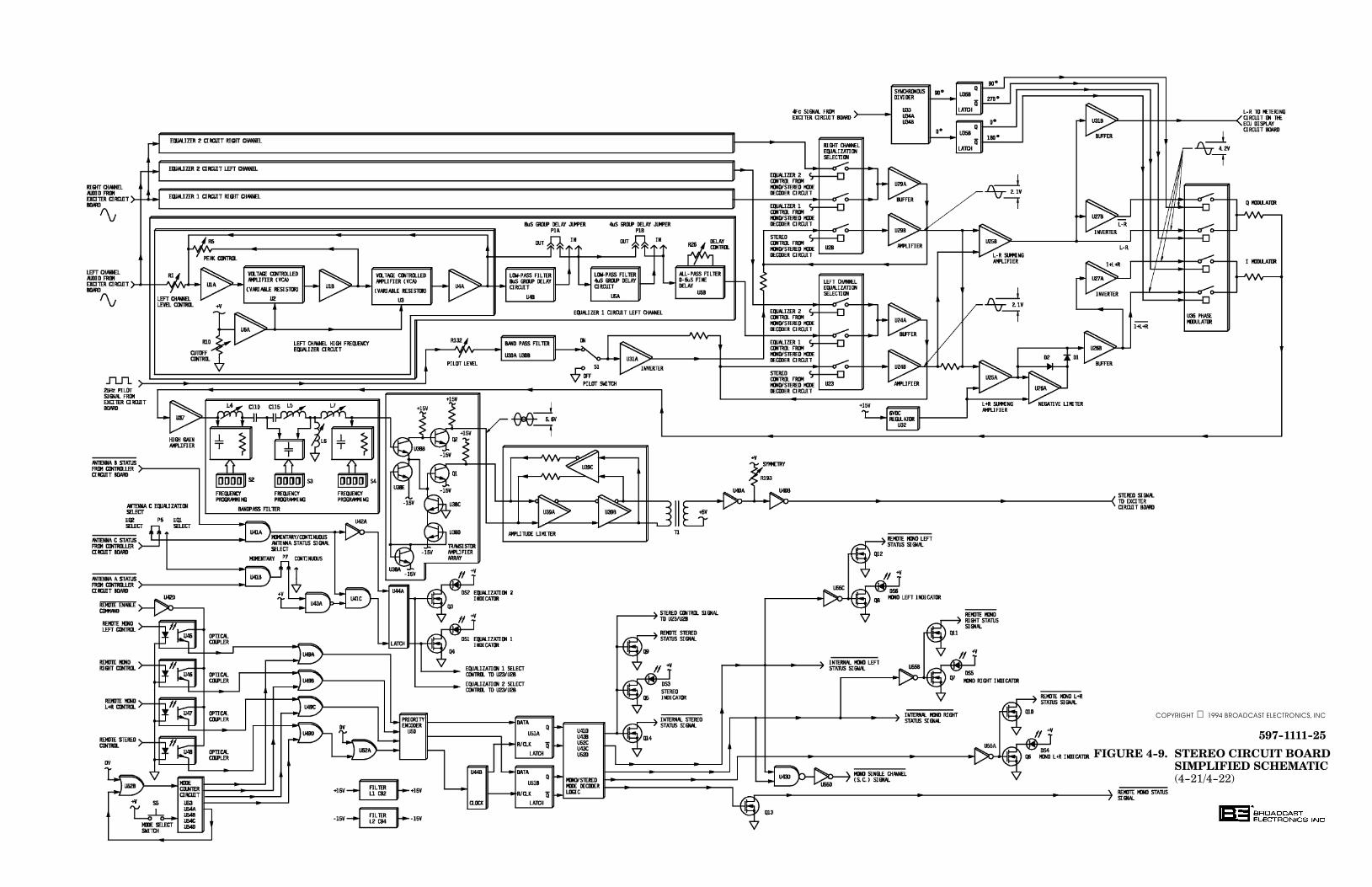
597-1111-25
FIGURE 4-9. STEREO CIRCUIT BOARD SIMPLIFIED SCHEMATIC(4-21/4-22)
COPYRIGHT 1994 BROADCAST ELECTRONICS, INC
5-1
WARNING: DISCONNECT POWER PRIOR TO SERVICING
SECTION V
MAINTENANCE
5-1. INTRODUCTION.
5-2. This section provides maintenance information, electrical adjustment procedures, and
troubleshooting information for the Broadcast Electronics AM-1A/AM-500A transmitters.
5-3. SAFETY CONSIDERATIONS.
WARNING
WARNING
WARNING
WARNING
THE TRANSMITTER CONTAINS MULTIPLE CIRCUIT
GROUNDS WITH HIGH AC AND DC POTENTIALS
WITH RESPECT TO THE CHASSIS WHICH IS AT
EARTH POTENTIAL. DO NOT ENERGIZE THE
TRANSMITTER WITH TEST EQUIPMENT CON�
NECTED TO THE TRANSMITTER OUTPUT
NETWORK, RF POWER MODULE, RF COMBINER, OR
POWER SUPPLY COMPONENTS.
5-4. The AM-1A/AM-500A transmitters contain high voltages and currents. If safety
precautions are not practiced, contact with the high voltages and currents could cause
serious injury or death. The transmitter is equipped with many built-in safety features,
however good judgement, care, and common sense must be practiced to prevent accidents.
5-5. In addition to high voltages and currents, the transmitter contain multiple circuit grounds
with high ac and dc potentials with respect to the chassis which is at earth potential. The
potentials could cause serious injury or death if maintenance personnel simultaneously
touch a circuit ground and the chassis. As a result, operation of the transmitter with test
equipment connected to transmitter RF power module, bandpass filter, combiner, or power
supply components is extremely dangerous and must not be attempted. Therefore, never
energize the transmitter with test equipment connected to the transmitter RF power
module, bandpass filter, combiner, or power supply components. Test equipment may be
connected to the ECU circuit boards from the front of the transmitter using the supplied
extender circuit board with power energized. The maintenance procedures presented in
this section should be performed only by trained and experienced maintenance personnel.
5-6. The transmitter output network chassis design will not allow access to the components
without the disconnection of the ac input and the RF output. Never re-connect the AC
input or the RF output with the top-panel removed.
5-7. FIRST LEVEL MAINTENANCE.
5-8. First level maintenance consists of procedures applied to the equipment to prevent future
failures. The procedures are performed on a regular basis and the results recorded in a
maintenance log. Preventive maintenance of the transmitter consists of good
housekeeping and checking performance levels using the meters and various indicators
built into the equipment.
5-2
WARNING: DISCONNECT POWER PRIOR TO SERVICING
5-9. ROUTINE MAINTENANCE.
WARNING
WARNING
NEVER OPEN THE EQUIPMENT UNLESS ALL TRANS�
MITTER PRIMARY POWER IS DISCONNECTED. EN�
SURE ALL TRANSMITTER PRIMARY POWER IS DIS�
CONNECTED BEFORE ATTEMPTING MAINTENANCE
ON ANY AREA WITHIN THE TRANSMITTER.
5-10. INSPECTION AND CLEANING. On a regular basis, clean the equipment of accumulated
dust using a brush and vacuum cleaner. Inspect the modulator circuit board, RF amplifier
circuit boards, and the power supply circuit board for damage caused by components
overheating. Overheated components are identified by circuit board discoloration near the
component leads. Inspect the circuit boards for loose hardware as required.
5-11. CONTROLLER BATTERY. Periodically, the controller battery in the ECU assembly should
be checked by depressing the battery test switch on the controller circuit board. The
battery test indicator will illuminate to indicate the battery is operational. If the battery
test indicator fails to illuminate, the battery must be replaced. A good-quality Alkaline
battery is recommended for replacement. Typically, it is recommended the controller
battery be replaced annually.
5-12. AIR FILTER. The transmitter is equipped with a screen type air filter. The screen filter is
designed to be removed and cleaned using a brush and vacuum. Check the filter
approximately once a week. Remove dirt from the filter as-required by: 1) removing the
filter from the chassis and 2) cleaning the filter using a brush and vacuum.
5-13. FLUSHING FAN. Inspect the transmitter flushing fan for dust accumulation and
periodically clean the fan using a brush and vacuum cleaner. Do not use compressed air
and an air gun. The fan is cooled by air passing around the motor. If dust is allowed to
accumulate on the motor, the ambient air temperature will increase due to restricted air
flow. When the ambient air temperature increases, the fan motor bearing lubricant will
gradually vaporize and bearing failure will occur.
5-14. It is recommended the flushing fan mounting hardware be periodically checked. The
flushing fan is equipped with sealed bearings which do not permit lubrication. If a bearing
fails, the motor must be replaced.
5-15. SPARK GAP. The output network chassis is equipped with a spark gap. The spark gap
is provided to safely conduct lightning potentials appearing at the transmitter output to
ground. Inspect the spark gap annually to ensure the gap is operational.
5-16. SECOND LEVEL MAINTENANCE.
5-17. Second level maintenance consists of procedures required to adjust the transmitter
circuitry or restore the transmitter to operation after a fault has occurred. The procedures
consists of electrical adjustments, troubleshooting, and component replacement
procedures.
5-3
WARNING: DISCONNECT POWER PRIOR TO SERVICING
WARNING
WARNING
NEVER OPEN THE EQUIPMENT UNLESS ALL TRANS�
MITTER PRIMARY POWER IS DISCONNECTED. EN�
SURE ALL TRANSMITTER PRIMARY POWER IS DIS�
CONNECTED BEFORE ATTEMPTING MAINTENANCE
ON ANY AREA WITHIN THE TRANSMITTER.
5-18. The maintenance philosophy for the transmitter consists of isolating a problem to a specific
area. Once the specific area is located, subsequent troubleshooting using the information
in the following text will assist in problem isolation to a replaceable assembly or
component. If required, the assembly may be: 1) returned to the factory for repair or
exchange or 2) repaired locally.
5-19. OVERALL TRANSMITTER.
5-20. ELECTRICAL ADJUSTMENTS.
WARNING
WARNING
NEVER OPEN THE EQUIPMENT UNLESS ALL TRANS�
MITTER PRIMARY POWER IS DISCONNECTED. EN�
SURE ALL TRANSMITTER PRIMARY POWER IS DIS�
CONNECTED BEFORE ATTEMPTING MAINTENANCE
ON ANY AREA WITHIN THE TRANSMITTER.
5-21. TRANSMITTER FREQUENCY RE-PROGRAMMING.
5-22. The AM-1A/AM-500A transmitters are configured for a specific frequency when shipped
from the factory. The transmitter is equipped with several frequency dependent parts and
circuits. Due to the frequency dependent parts, frequency dependent circuits, and
specialized procedures, the transmitter can not be reprogrammed for a different frequency
in the field. If the transmitter is required to be programmed for a different frequency,
contact the Broadcast Electronics Customer Service department.
5-23. TROUBLESHOOTING.
WARNING
WARNING
WARNING
WARNING
THE TRANSMITTER CONTAINS MULTIPLE CIRCUIT
GROUNDS WITH HIGH AC AND DC POTENTIALS
WITH RESPECT TO THE CHASSIS WHICH IS AT
EARTH POTENTIAL. DO NOT ENERGIZE THE
TRANSMITTER WITH TEST EQUIPMENT CON�
NECTED TO THE TRANSMITTER BANDPASS FILTER,
RF POWER MODULE, COMBINER, OR POWER SUPPLY
COMPONENTS.
5-24. The AM-1A/AM-500A transmitters are equipped with extensive indicator and meter
circuitry to allow the operator to isolate problems to a specific area within the transmitter.
Due to the hazardous voltages and currents contained in the equipment, operation of the
transmitter with test equipment connected to the transmitter RF power module, bandpass
filter, combiner, or power supply components is extremely dangerous and must not be
attempted. Test equipment may be connected to the ECU circuit boards from the front of
the transmitter using the supplied extender circuit board with power energized.
Therefore, the transmitter indicators and meters must be used to isolate a problem to a
specific area.
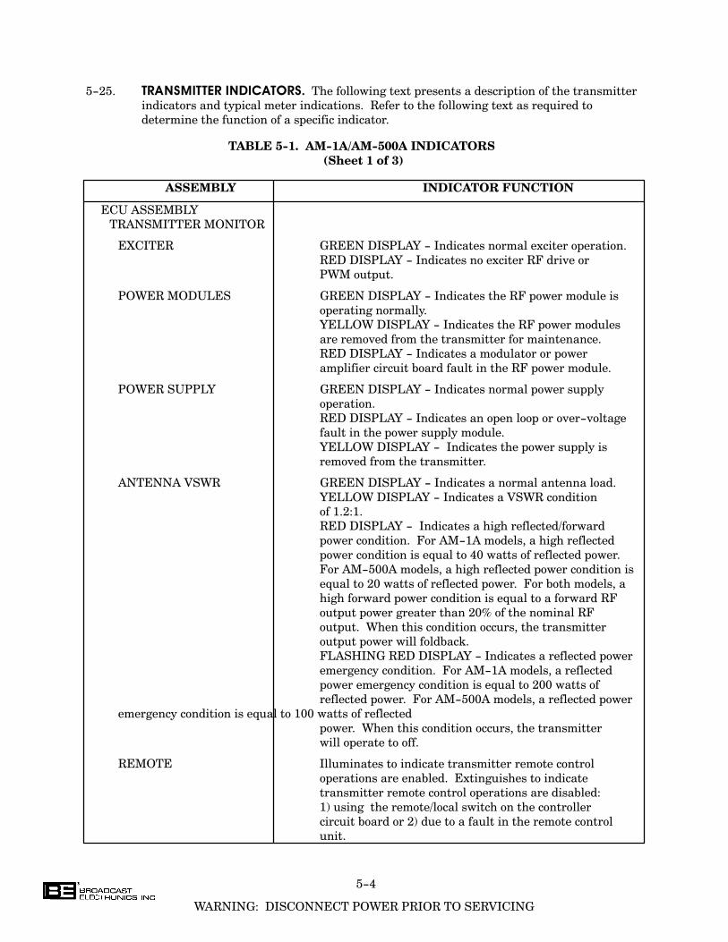
5-4
WARNING: DISCONNECT POWER PRIOR TO SERVICING
5-25. TRANSMITTER INDICATORS. The following text presents a description of the transmitter
indicators and typical meter indications. Refer to the following text as required to
determine the function of a specific indicator.
TABLE 5-1. AM-1A/AM-500A INDICATORS
(Sheet 1 of 3)
ASSEMBLY INDICATOR FUNCTION
ECU ASSEMBLY
TRANSMITTER MONITOR
EXCITER GREEN DISPLAY - Indicates normal exciter operation.
RED DISPLAY - Indicates no exciter RF drive or
PWM output.
POWER MODULES GREEN DISPLAY - Indicates the RF power module is
operating normally.
YELLOW DISPLAY - Indicates the RF power modules
are removed from the transmitter for maintenance.
RED DISPLAY - Indicates a modulator or power
amplifier circuit board fault in the RF power module.
POWER SUPPLY GREEN DISPLAY - Indicates normal power supply
operation.
RED DISPLAY - Indicates an open loop or over-voltage
fault in the power supply module.
YELLOW DISPLAY - Indicates the power supply is
removed from the transmitter.
ANTENNA VSWR GREEN DISPLAY - Indicates a normal antenna load.
YELLOW DISPLAY - Indicates a VSWR condition
of 1.2:1.
RED DISPLAY - Indicates a high reflected/forward
power condition. For AM-1A models, a high reflected
power condition is equal to 40 watts of reflected power.
For AM-500A models, a high reflected power condition is
equal to 20 watts of reflected power. For both models, a
high forward power condition is equal to a forward RF
output power greater than 20% of the nominal RF
output. When this condition occurs, the transmitter
output power will foldback.
FLASHING RED DISPLAY - Indicates a reflected power
emergency condition. For AM-1A models, a reflected
power emergency condition is equal to 200 watts of
reflected power. For AM-500A models, a reflected power
emergency condition is equal to 100 watts of reflected
power. When this condition occurs, the transmitter
will operate to off.
REMOTE Illuminates to indicate transmitter remote control
operations are enabled. Extinguishes to indicate
transmitter remote control operations are disabled:
1) using the remote/local switch on the controller
circuit board or 2) due to a fault in the remote control
unit.
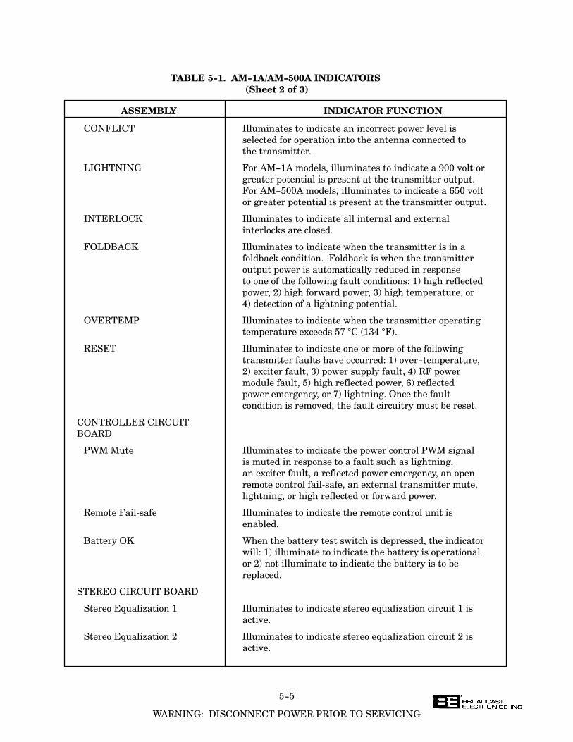
5-5
WARNING: DISCONNECT POWER PRIOR TO SERVICING
TABLE 5-1. AM-1A/AM-500A INDICATORS
(Sheet 2 of 3)
ASSEMBLY INDICATOR FUNCTION
CONFLICT Illuminates to indicate an incorrect power level is
selected for operation into the antenna connected to
the transmitter.
LIGHTNING For AM-1A models, illuminates to indicate a 900 volt or
greater potential is present at the transmitter output.
For AM-500A models, illuminates to indicate a 650 volt
or greater potential is present at the transmitter output.
INTERLOCK Illuminates to indicate all internal and external
interlocks are closed.
FOLDBACK Illuminates to indicate when the transmitter is in a
foldback condition. Foldback is when the transmitter
output power is automatically reduced in response
to one of the following fault conditions: 1) high reflected
power, 2) high forward power, 3) high temperature, or
4) detection of a lightning potential.
OVERTEMP Illuminates to indicate when the transmitter operating
temperature exceeds 57 °C (134 °F).
RESET Illuminates to indicate one or more of the following
transmitter faults have occurred: 1) over-temperature,
2) exciter fault, 3) power supply fault, 4) RF power
module fault, 5) high reflected power, 6) reflected
power emergency, or 7) lightning. Once the fault
condition is removed, the fault circuitry must be reset.
CONTROLLER CIRCUIT
BOARD
PWM Mute Illuminates to indicate the power control PWM signal
is muted in response to a fault such as lightning,
an exciter fault, a reflected power emergency, an open
remote control fail�safe, an external transmitter mute,
lightning, or high reflected or forward power.
Remote Fail�safe Illuminates to indicate the remote control unit is
enabled.
Battery OK When the battery test switch is depressed, the indicator
will: 1) illuminate to indicate the battery is operational
or 2) not illuminate to indicate the battery is to be
replaced.
STEREO CIRCUIT BOARD
Stereo Equalization 1 Illuminates to indicate stereo equalization circuit 1 is
active.
Stereo Equalization 2 Illuminates to indicate stereo equalization circuit 2 is
active.
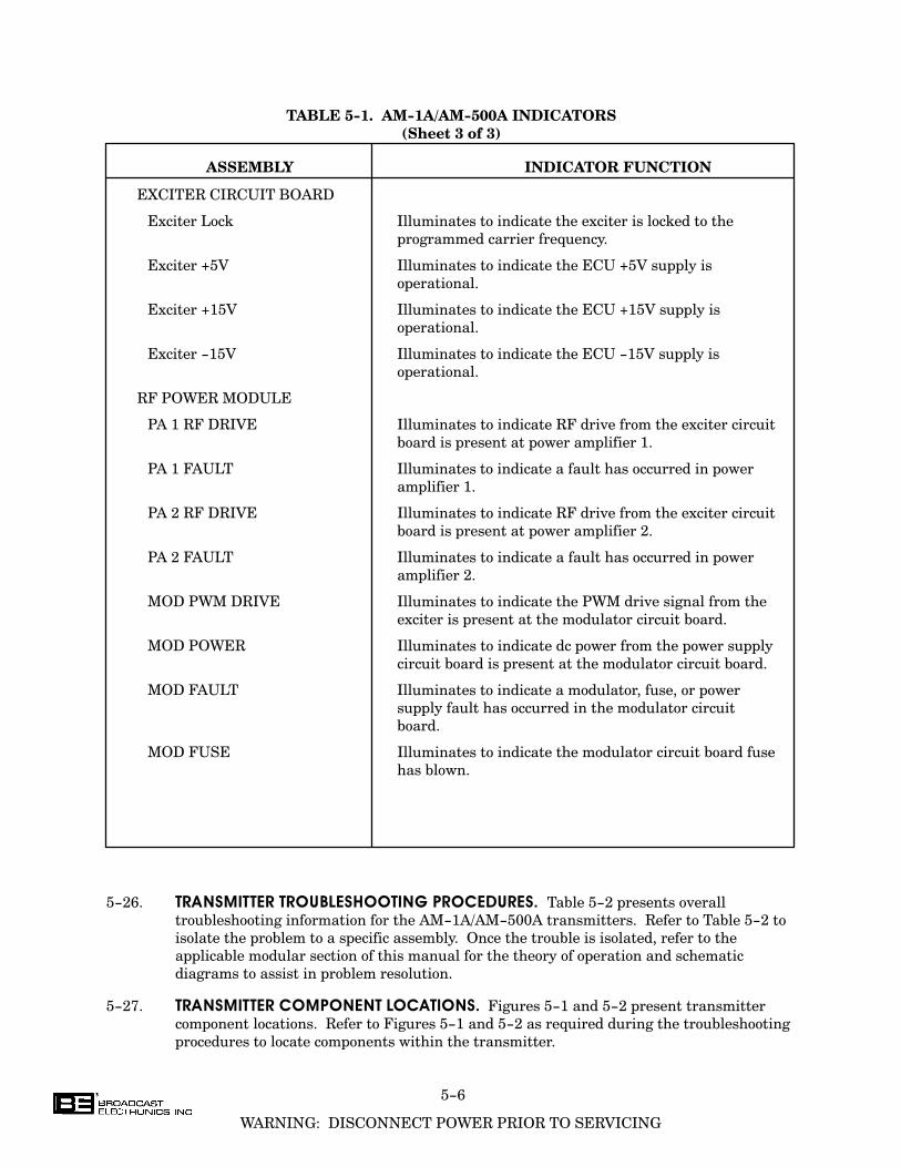
5-6
WARNING: DISCONNECT POWER PRIOR TO SERVICING
TABLE 5-1. AM-1A/AM-500A INDICATORS
(Sheet 3 of 3)
ASSEMBLY INDICATOR FUNCTION
EXCITER CIRCUIT BOARD
Exciter Lock Illuminates to indicate the exciter is locked to the
programmed carrier frequency.
Exciter +5V Illuminates to indicate the ECU +5V supply is
operational.
Exciter +15V Illuminates to indicate the ECU +15V supply is
operational.
Exciter -15V Illuminates to indicate the ECU -15V supply is
operational.
RF POWER MODULE
PA 1 RF DRIVE Illuminates to indicate RF drive from the exciter circuit
board is present at power amplifier 1.
PA 1 FAULT Illuminates to indicate a fault has occurred in power
amplifier 1.
PA 2 RF DRIVE Illuminates to indicate RF drive from the exciter circuit
board is present at power amplifier 2.
PA 2 FAULT Illuminates to indicate a fault has occurred in power
amplifier 2.
MOD PWM DRIVE Illuminates to indicate the PWM drive signal from the
exciter is present at the modulator circuit board.
MOD POWER Illuminates to indicate dc power from the power supply
circuit board is present at the modulator circuit board.
MOD FAULT Illuminates to indicate a modulator, fuse, or power
supply fault has occurred in the modulator circuit
board.
MOD FUSE Illuminates to indicate the modulator circuit board fuse
has blown.
5-26. TRANSMITTER TROUBLESHOOTING PROCEDURES. Table 5-2 presents overall
troubleshooting information for the AM-1A/AM-500A transmitters. Refer to Table 5-2 to
isolate the problem to a specific assembly. Once the trouble is isolated, refer to the
applicable modular section of this manual for the theory of operation and schematic
diagrams to assist in problem resolution.
5-27. TRANSMITTER COMPONENT LOCATIONS. Figures 5-1 and 5-2 present transmitter
component locations. Refer to Figures 5-1 and 5-2 as required during the troubleshooting
procedures to locate components within the transmitter.

5-7
WARNING: DISCONNECT POWER PRIOR TO SERVICING
TABLE 5-2. AM-1A/AM-500A TROUBLESHOOTING
(Sheet 1 of 4)
SYMPTOM CIRCUITRY TO CHECK
1. NO OUTPUT POWER 1. Check the ac line voltage using the reflected power/
2. NO NORMAL/FAULT ac voltage meter. If no line voltage is present, check
INDICATIONS circuit breaker CB1.
2. Check the ±15 volt and +5 volt indicators on the
exciter circuit board. If no indicators are
illuminated, check the ECU power supply.
1. NO OUTPUT POWER 1. Transmitter operated to off due to 7 on/off cycles
2. NORMAL INDICATIONS within 15 seconds. Operate the transmitter to on
3. NO CONTROL OPERATIONS as follows: 1) do not depress any controller
switch/indicators for approximately 30 seconds and
2) depress the desired power level switch/indicator.
2. Refer to POWER SUPPLY troubleshooting and
troubleshoot the power supply circuit board for no
120 Hz signal output.
1. RED TRANSMITTER 1. Check the lock indicator on the exciter circuit
MONITOR EXCITER board. If the lock indicator is not illuminated, refer
INDICATION to ECU troubleshooting and troubleshoot the exciter
circuit board for lock indicator extinguished.
2. Remove the stereo circuit board and perform the
following: 1) depress the RESET switch and
2) initiate transmitter operation. If the transmitter
will not operate, refer to ECU troubleshooting and
troubleshoot the exciter circuit board. If the
transmitter operates, refer to ECU troubleshooting
and troubleshoot the stereo circuit board.
1. YELLOW TRANSMITTER 1. Indicates the RF power module is removed from the
MONITOR POWER MODULE transmitter.
INDICATION
1. RED TRANSMITTER MONITOR 1. Refer to RF POWER MODULE troubleshooting and
POWER MODULE FAULT troubleshoot the RF power module.
INDICATION 2. Visually inspect the RF power module combiner
2. RED RF POWER MODULE for discolored components.
FAULT INDICATION
1. YELLOW TRANSMITTER 1. Indicates the power supply module is removed from
MONITOR POWER SUPPLY transmitter.
INDICATION
1. RED TRANSMITTER MONITOR 1. Check for an over-temperature condition by
POWER SUPPLY INDICATION inspecting the fan and the filter.
2. Refer to POWER SUPPLY MODULE troubleshooting
and troubleshoot the power supply module.

5-8
WARNING: DISCONNECT POWER PRIOR TO SERVICING
TABLE 5-2. AM-1A/AM-500A TROUBLESHOOTING
(Sheet 2 of 4)
SYMPTOM CIRCUITRY TO CHECK
1. YELLOW TRANSMITTER 1. Check the antenna and phasor equipment.
MONITOR ANTENNA 2. Refer to DIRECTIONAL COUPLER/LIGHTNING
INDICATION DETECTION/LIGHTNING PROTECTION CIRCUIT
BOARD troubleshooting and troubleshoot the
directional coupler circuit board.
1. RED TRANSMITTER MONITOR 1. Check the antenna and phasor equipment.
ANTENNA INDICATION 2. Refer to DIRECTIONAL COUPLER/LIGHTNING
DETECTION/LIGHTNING PROTECTION CIRCUIT
BOARD troubleshooting and troubleshoot the
directional coupler circuit board.
1. FLASHING RED TRANSMITTER 1. Check the antenna and phasor equipment.
MONITOR ANTENNA 2. Visually inspect the spark gap for a short circuit
INDICATION condition.
3. Check the lightning protection circuit board for a
short circuit condition.
1. INTERLOCK INDICATOR 1. Operate remote/local switch to local.
EXTINGUISHED WHEN IN THE A. If the interlock indicator illuminates, ensure
REMOTE CONTROL MODE a +5 volt signal is applied to remote fail�safe
input TB1-28 on the ECU rear-panel when the
remote control unit is enabled.
1. If the +5 volt signal is not present, troubleshoot
the remote control unit.
2. If the +5 volt signal is present, check Q48 and
U56 on the controller circuit board.
B. If the interlock indicator is extinguished,
check the cabinet and the external interlocks.
1. CONFLICT INDICATION 1. Ensure a +5 volt status signal from the selected
antenna is applied to the antenna A, B, or C input
on the ECU rear-panel.
2. Ensure the correct transmitter power level is
selected for operation into the antenna.
3. Check the antenna interlock circuit programming on
the controller circuit board.
4. Refer to ECU troubleshooting and troubleshoot the
controller circuit board for a conflict indication.
1. NO OUTPUT POWER 1. Transmitter operated to off due to 7 on/off cycles
2. LIGHTNING INDICATOR within 15 seconds. Operate the transmitter to on
ILLUMINATED as follows: 1) do not depress any controller
switch/indicators for approximately 30 seconds and
2) depress the desired power level switch/indicator.
2. Check Q401 on the lightning detection circuit board.
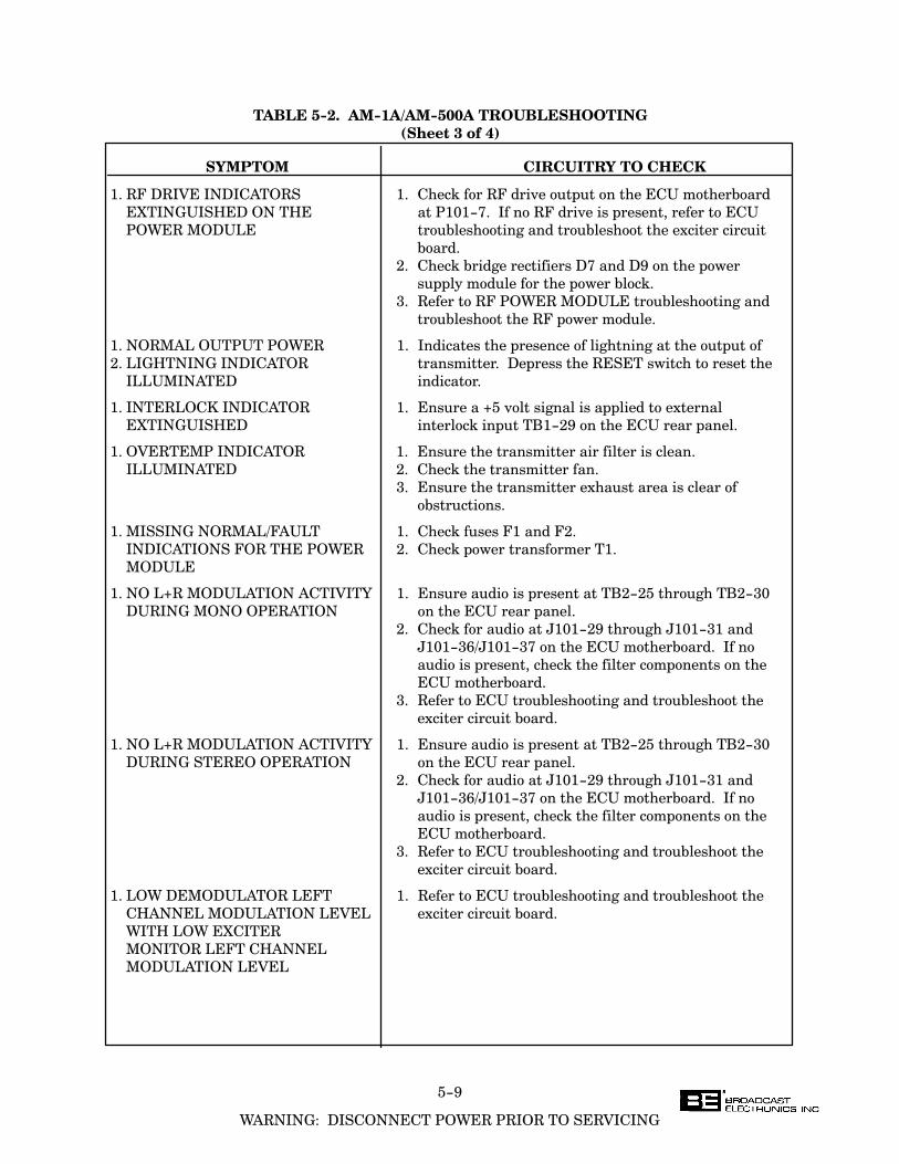
5-9
WARNING: DISCONNECT POWER PRIOR TO SERVICING
TABLE 5-2. AM-1A/AM-500A TROUBLESHOOTING
(Sheet 3 of 4)
SYMPTOM CIRCUITRY TO CHECK
1. RF DRIVE INDICATORS 1. Check for RF drive output on the ECU motherboard
EXTINGUISHED ON THE at P101-7. If no RF drive is present, refer to ECU
POWER MODULE troubleshooting and troubleshoot the exciter circuit
board.
2. Check bridge rectifiers D7 and D9 on the power
supply module for the power block.
3. Refer to RF POWER MODULE troubleshooting and
troubleshoot the RF power module.
1. NORMAL OUTPUT POWER 1. Indicates the presence of lightning at the output of
2. LIGHTNING INDICATOR transmitter. Depress the RESET switch to reset the
ILLUMINATED indicator.
1. INTERLOCK INDICATOR 1. Ensure a +5 volt signal is applied to external
EXTINGUISHED interlock input TB1-29 on the ECU rear panel.
1. OVERTEMP INDICATOR 1. Ensure the transmitter air filter is clean.
ILLUMINATED 2. Check the transmitter fan.
3. Ensure the transmitter exhaust area is clear of
obstructions.
1. MISSING NORMAL/FAULT 1. Check fuses F1 and F2.
INDICATIONS FOR THE POWER 2. Check power transformer T1.
MODULE
1. NO L+R MODULATION ACTIVITY 1. Ensure audio is present at TB2-25 through TB2-30
DURING MONO OPERATION on the ECU rear panel.
2. Check for audio at J101-29 through J101-31 and
J101-36/J101-37 on the ECU motherboard. If no
audio is present, check the filter components on the
ECU motherboard.
3. Refer to ECU troubleshooting and troubleshoot the
exciter circuit board.
1. NO L+R MODULATION ACTIVITY 1. Ensure audio is present at TB2-25 through TB2-30
DURING STEREO OPERATION on the ECU rear panel.
2. Check for audio at J101-29 through J101-31 and
J101-36/J101-37 on the ECU motherboard. If no
audio is present, check the filter components on the
ECU motherboard.
3. Refer to ECU troubleshooting and troubleshoot the
exciter circuit board.
1. LOW DEMODULATOR LEFT 1. Refer to ECU troubleshooting and troubleshoot the
CHANNEL MODULATION LEVEL exciter circuit board.
WITH LOW EXCITER
MONITOR LEFT CHANNEL
MODULATION LEVEL

5-10
WARNING: DISCONNECT POWER PRIOR TO SERVICING
TABLE 5-2. AM-1A/AM-500A TROUBLESHOOTING
(Sheet 4 of 4)
SYMPTOM CIRCUITRY TO CHECK
1. LOW DEMODULATOR RIGHT 1. Refer to ECU troubleshooting and troubleshoot the
CHANNEL MODULATION LEVEL exciter circuit board.
WITH LOW EXCITER
MONITOR RIGHT CHANNEL
MODULATION LEVEL
1. LOW DEMODULATOR LEFT 1. Refer to ECU troubleshooting and troubleshoot the
CHANNEL MODULATION LEVEL stereo circuit board.
WITH NORMAL EXCITER
MONITOR LEFT CHANNEL
MODULATION LEVEL
1. LOW DEMODULATOR RIGHT 1. Refer to ECU troubleshooting and troubleshoot the
CHANNEL MODULATION LEVEL stereo circuit board.
WITH NORMAL EXCITER
MONITOR RIGHT CHANNEL
MODULATION LEVEL
1. PWM DRIVE INDICATOR 1. Check for a 0V to 15V PWM output at the anode of
EXTINGUISHED ON THE D6, D8, D10, D12, D14, D16, D18, D20, D47, and D49
RF POWER MODULE on the exciter circuit board.
A. If the PWM output is not present, refer to ECU
troubleshooting and troubleshoot the exciter
circuit board.
B. If the PWM output is present, refer to RF POWER
MODULE troubleshooting and troubleshoot the
RF power module.
1. MOD PWR INDICATORS 1. Check for a power control PWM signal at the
EXTINGUISHED ON THE POWER drain of Q22 on the controller circuit board.
AMPLIFIER MODULE A. If the PWM signal is not present, refer to the
ECU section and troubleshoot the controller
circuit board for no power control PWM signal.
B. If the PWM output is present, check for a LOW at
Q13 on the controller circuit board.
1. If the LOW at Q13 is not present, refer to the
ECU section and troubleshoot the controller
circuit board for no transmitter on signal.
2. If the LOW at Q13 is present, refer to POWER
SUPPLY troubleshooting and troubleshoot the
power supply for no MOD POWER indicator.
1. REFLECTED POWER METER 1. Narrow-band antenna. Contact the Broadcast
FLUCTUATES WITH Electronics Customer Service Department.
MODULATION
1. FORWARD POWER METER 1. Enable the high-pass filter on the exciter circuit
FLUCTUATES WITH board.
MODULATION
5-11
WARNING: DISCONNECT POWER PRIOR TO SERVICING
5-28. POWER SUPPLY CIRCUIT BOARD.
WARNING
WARNING
WARNING
WARNING
THE TRANSMITTER CONTAINS MULTIPLE CIRCUIT
GROUNDS WITH HIGH AC AND DC POTENTIALS
WITH RESPECT TO THE CHASSIS WHICH IS AT
EARTH POTENTIAL. DO NOT ENERGIZE THE
TRANSMITTER WITH TEST EQUIPMENT CON�
NECTED TO THE TRANSMITTER BANDPASS FILTER,
RF POWER MODULE, COMBINER, OR POWER SUPPLY
COMPONENTS.
WARNING
WARNING
NEVER RE-CONNECT AC POWER OR THE RF OUT�
PUT TO THE OUTPUT NETWORK CHASSIS WITH THE
TOP-PANEL REMOVED.
5-29. SAFETY CONSIDERATIONS.
5-30. The AM-1A/AM-500A transmitters are equipped with extensive indicator and meter
circuitry to allow the operator to isolate problems to a specific area within the transmitter.
Due to the hazardous voltages and currents contained in the equipment, operation of the
transmitter with test equipment connected to the transmitter RF power module, bandpass
filter, combiner, or power supply components is extremely dangerous and must not be
attempted. Test equipment may be connected to the ECU circuit boards from the front of
the transmitter using the supplied extender circuit board with power energized.
Therefore, the transmitter indicators and meters must be used to isolate a problem to a
specific area.
5-31. REMOVING/INSTALLING A POWER SUPPLY CIRCUIT BOARD.
5-32. The power supply circuit board is removed by disconnecting three connectors, loosening the
mounting hardware, and sliding the circuit board from the mounting pins. To remove or
install the power supply circuit board, proceed as follows:
WARNING
WARNING
DISCONNECT ALL TRANSMITTER PRIMARY POWER
BEFORE PROCEEDING.
5-33. Disconnect all transmitter primary power.
5-34. To remove the power supply circuit board, proceed as follows:
1. Refer to Figure 5-1 and locate the power supply circuit board.
2. Disconnect connectors P1, P2, and P3 on the circuit board assembly.
3. Loosen the power supply circuit board mounting hardware.
4. Lift the circuit board from the mounting pins and remove the circuit board from
the chassis.
5-35. TROUBLESHOOTING PROCEDURES.
5-36. The power supply module troubleshooting procedures are presented in Table 5-3. During
the execution of the troubleshooting information, perform all the procedures for a
symptom. The symptom may contain multiple component failures. Once the trouble is
isolated, refer to the circuit board theory of operation in SECTION IV and the schematic
diagrams to assist in problem resolution.
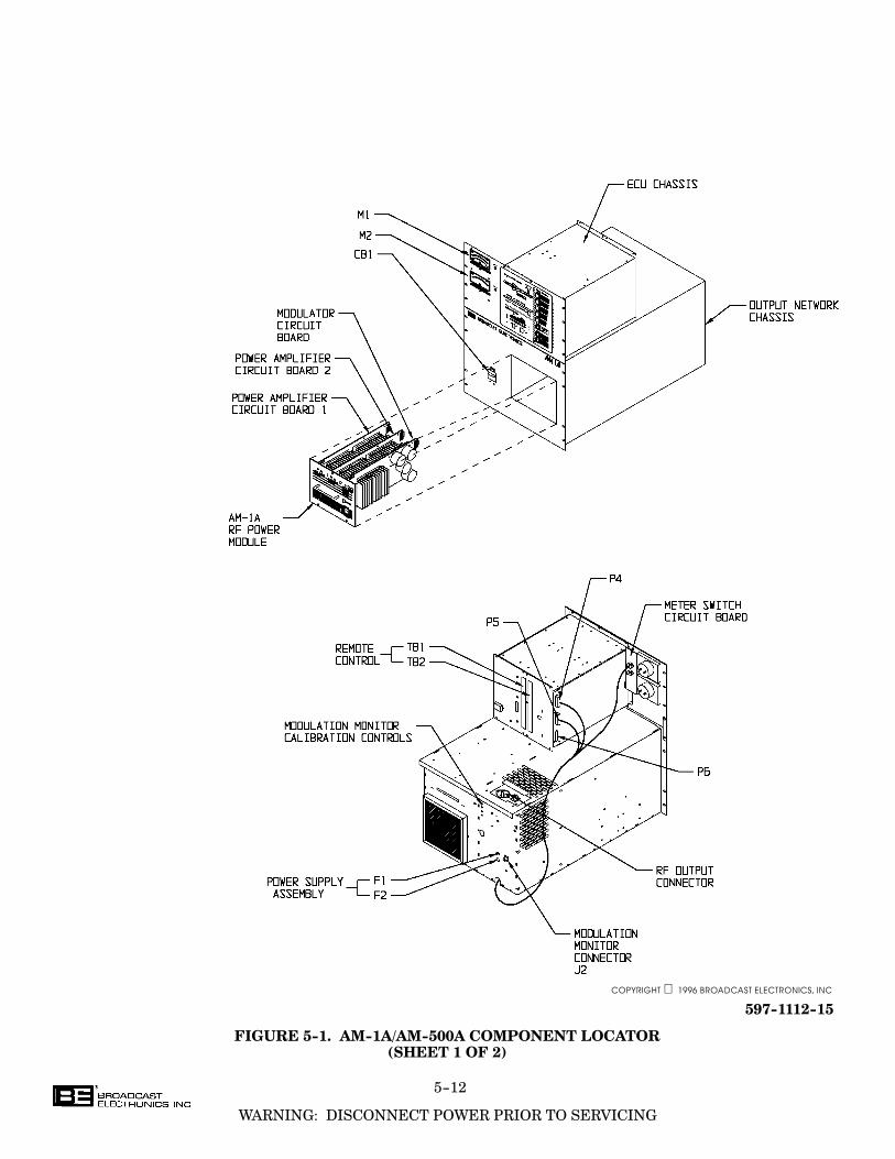
5-12
WARNING: DISCONNECT POWER PRIOR TO SERVICING
COPYRIGHT 1996 BROADCAST ELECTRONICS, INC
597-1112-15
FIGURE 5-1. AM-1A/AM-500A COMPONENT LOCATOR(SHEET 1 OF 2)
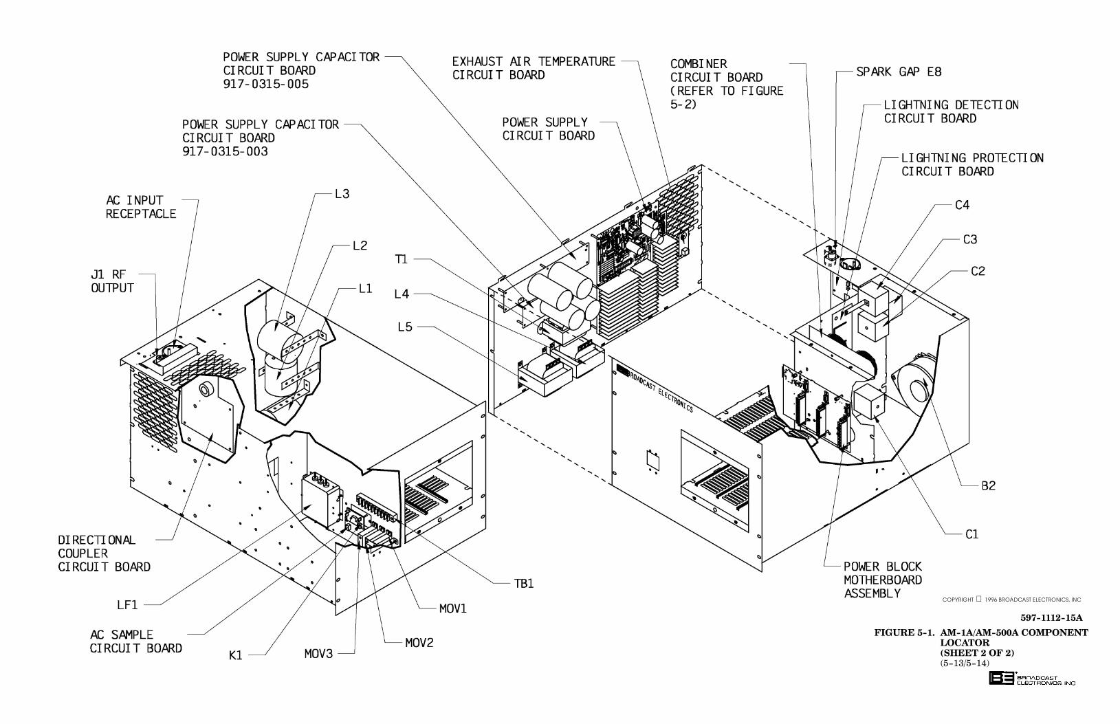
597-1112-15A
FIGURE 5-1. AM-1A/AM-500A COMPONENT LOCATOR(SHEET 2 OF 2)(5-13/5-14)
COPYRIGHT 1996 BROADCAST ELECTRONICS, INC
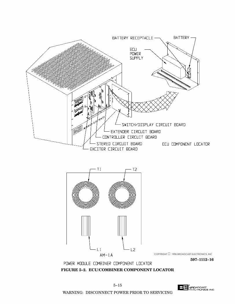
5-15
WARNING: DISCONNECT POWER PRIOR TO SERVICING
COPYRIGHT 1996 BROADCAST ELECTRONICS, INC
597-1112-16
FIGURE 5-2. ECU/COMBINER COMPONENT LOCATOR
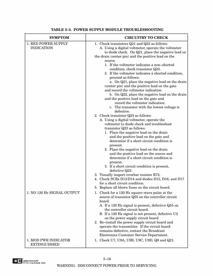
5-16
WARNING: DISCONNECT POWER PRIOR TO SERVICING
TABLE 5-3. POWER SUPPLY MODULE TROUBLESHOOTING
SYMPTOM CIRCUITRY TO CHECK
1. RED POWER SUPPLY 1. Check transistors Q21 and Q22 as follows:
INDICATION A. Using a digital voltmeter, operate the voltmeter
to diode check. On Q21, place the negative lead on
the drain (center pin) and the positive lead on the
source.
1. If the voltmeter indicates a non-shorted
condition, check transistor Q23.
2. If the voltmeter indicates a shorted condition,
proceed as follows:
a. On Q21, place the negative lead on the drain
(center pin) and the positive lead on the gate
and record the voltmeter indication.
b. On Q22, place the negative lead on the drain
and the positive lead on the gate and
record the voltmeter indication.
c. The transistor with the lowest voltage is
defective.
2. Check transistor Q23 as follows:
A. Using a digital voltmeter, operate the
voltmeter to diode check and troubleshoot
transistor Q23 as follows:
1. Place the negative lead on the drain
and the positive lead on the gate and
determine if a short circuit condition is
present.
2. Place the negative lead on the drain
and the positive lead on the source and
determine if a short circuit condition is
present.
3. If a short circuit condition is present,
defective Q23.
3. Visually inspect crowbar resistor R72.
4. Check SCRs D13/D14 and diodes D15, D16, and D17
for a short circuit condition.
5. Replace all blown fuses on the circuit board.
1. NO 120 Hz SIGNAL OUTPUT 1. Check for a 120 Hz square-wave pulse at the
source of transistor Q55 on the controller circuit
board.
A. If a 120 Hz signal is present, defective Q55 on
the controller circuit board.
B. If a 120 Hz signal is not present, defective U2
on the power supply circuit board.
2. Re-install the power supply circuit board and
operate the transmitter. If the circuit board
remains defective, contact the Broadcast
Electronics Customer Service Department.
1. MOD PWR INDICATOR 1. Check U7, U9A, U9B, U9C, U9D, Q9 and Q21.
EXTINGUISHED

5-17
WARNING: DISCONNECT POWER PRIOR TO SERVICING
5-37. RF POWER MODULE.
WARNING
WARNING
WARNING
WARNING
THE TRANSMITTER CONTAINS MULTIPLE CIRCUIT
GROUNDS WITH HIGH AC AND DC POTENTIALS
WITH RESPECT TO THE CHASSIS WHICH IS AT
EARTH POTENTIAL. DO NOT ENERGIZE THE
TRANSMITTER WITH TEST EQUIPMENT CON�
NECTED TO THE TRANSMITTER BANDPASS FILTER,
RF POWER MODULE, COMBINER, OR POWER SUPPLY
COMPONENTS.
WARNING
WARNING
NEVER RE-CONNECT AC POWER OR THE RF OUT�
PUT TO THE OUTPUT NETWORK CHASSIS WITH THE
TOP-PANEL REMOVED.
5-38. SAFETY CONSIDERATIONS.
5-39. The AM-1A/AM-500A transmitters are equipped with extensive indicator and meter
circuitry to allow the operator to isolate problems to a specific area within the transmitter.
Due to the hazardous voltages and currents contained in the equipment, operation of the
transmitter with test equipment connected to the transmitter RF power module, bandpass
filter, combiner, or power supply components is extremely dangerous and must not be
attempted. Test equipment may be connected to the ECU circuit boards from the front of
the transmitter using the supplied extender circuit board with power energized.
Therefore, the transmitter indicators and meters must be used to isolate a problem to a
specific area.
5-40. RF POWER MODULE ASSEMBLY PROCEDURE.
5-41. In the event of a failure in an RF power module, the module will be required to be
disassembled. The module must be properly re-assembled to prevent circuit board and
connector mis-alignment. To re-assemble an RF power module, proceed as follows:
1. Locate the PA 2 circuit board and install the hex standoffs in the four locations
at the rear of the circuit board.
2. Locate the PA 1 circuit board and install the front panel mounting bracket
using the four Phillips-head screws. Do not secure the screws at this time.
Repeat the procedure for the PA2 circuit board and the modulator circuit
board.
3. Install the PA 1 circuit board in the PA 1 location on the RF power module
front panel. Secure the circuit board bracket to the front panel using the hex
nuts. Repeat the procedure for the PA 2 and modulator circuit boards.
4. Place the RF power module on a square and flat surface such as a table with
the top of the module facing up.
5. Place the module front panel flush with the edge of the table and align the
circuit boards as follows:
A. Move the PA 1 circuit board until the front of the circuit board is flush with
the RF module front panel and the top edge of the circuit board is straight.
B. Secure the two Phillips-head screws which mount the circuit board to the
bracket.
C. Repeat the procedure for the PA 2 and modulator circuit boards.
5-18
WARNING: DISCONNECT POWER PRIOR TO SERVICING
6. Rotate the module and repeat the alignment procedure for the bottom circuit
board bracket screws. Secure the two Phillips-head screws mounting the
circuit board to the bracket when each circuit board is properly aligned.
7. Install the hardware securing the PA 1 circuit board and the modulator circuit
board to the standoffs.
5-42. RF POWER MODULE EXCHANGE PROGRAM.
5-43. If an RF power module is determined to be defective, Broadcast Electronics has established
an RF power module exchange program. The program allows the customer to exchange a
defective module for a re-conditioned module. Terms of the program are available from
the Broadcast Electronics RF Customer Service Department. If an RF power module is
determined to be defective, troubleshoot the module or contact the Broadcast Electronics
RF Customer Service department for terms of the module exchange program.
5-44. TROUBLESHOOTING PROCEDURES.
5-45. The RF power module troubleshooting procedures are presented in Table 5-4. During the
execution of the procedures, perform all troubleshooting procedures for a symptom. The
symptom may contain multiple component failures. Once the trouble is isolated, refer to
the circuit board theory of operation in SECTION IV and the schematic diagrams to assist
in problem resolution.
TABLE 5-4. RF POWER MODULE TROUBLESHOOTING
(Sheet 1 of 3)
SYMPTOM CIRCUITRY TO CHECK
1. RF DRIVE INDICATOR 1. Using a digital voltmeter, operate the
EXTINGUISHED OR FLICKERING voltmeter to diode check and determine a
OR FAULT INDICATOR reference voltage for the transistors on the non-
ILLUMINATED defective power amplifier circuit board as follows:
A. Place the negative lead on the drain of Q1
(center pin) and the positive lead on the gate
and determine the voltage. The voltage using a
Fluke 77 meter = .45.
B. Place the negative lead on the drain of Q1
and the positive lead on the source and
determine the voltage. The voltage using a
Fluke 77 meter = .45.
2. Using the voltmeter as described in the preceding
step, measure the drain-to-gate and
drain-to-source voltage of transistor Q1 on the
defective power amplifier circuit board.
A. If the voltage is greater than ±0.1 volt of
the reference, defective Q1, Q3, and Q5.
B. If the voltage is equal to the reference, repeat
the preceding step for transistor Q2 on
the defective power amplifier circuit board.

5-19
WARNING: DISCONNECT POWER PRIOR TO SERVICING
TABLE 5-4. RF POWER MODULE TROUBLESHOOTING
(Sheet 2 of 3)
SYMPTOM CIRCUITRY TO CHECK
RF DRIVE INDICATOR 3. Using a digital voltmeter, operate the voltmeter
EXTINGUISHED OR FLICKERING to diode check and troubleshoot transistor Q3 as
OR FAULT INDICATOR follows:
ILLUMINATED (Cont'd) A. Place the negative lead on the drain of Q3
(center pin) and the positive lead on the gate
and determine if a short circuit condition is
present.
B. Place the negative lead on the drain of Q3
and the positive lead on the source and determine
if a short circuit condition is present.
C. If a short circuit condition is present, defective
Q3.
4. Repeat the procedure for transistors Q4, Q5, and
Q6.
5. Visually inspect regulator U1 for broken leads.
6. Check and replace all blown fuses on the circuit
board.
1. MOD PWM DRIVE INDICATOR 1. Refer to RF DRIVE INDICATOR EXTINGUISHED
EXTINGUISHED AND FAULT OR FLICKERING OR FAULT INDICATOR
OR FUSE INDICATOR ILLUMINATED in the preceding text and
ILLUMINATED troubleshoot the power amplifier circuit board.
2. If no defective circuitry is located on the power
amplifier circuit board, refer to FAULT OR FUSE
INDICATOR ILLUMINATED in the following
text and troubleshoot the modulator circuit board.
1. FAULT OR FUSE INDICATOR 1. Visually inspect regulator U10 on the modulator
ILLUMINATED circuit board for broken leads.
2. Using a digital voltmeter, operate the voltmeter to
diode check and determine a reference voltage for the
transistors on a non-defective modulator circuit board
as follows:
A. Place the negative lead on the drain of Q1
(center pin) and the positive lead on the gate and
determine the voltage. The voltage using a Fluke
77 meter = 1.2V.
B. Place the negative lead on the drain of Q1 and the
positive lead on the source and determine the
voltage. The voltage using a Fluke 77 meter =
0.46V.
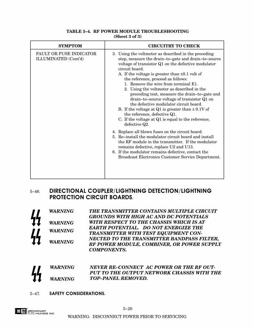
5-20
WARNING: DISCONNECT POWER PRIOR TO SERVICING
TABLE 5-4. RF POWER MODULE TROUBLESHOOTING
(Sheet 3 of 3)
SYMPTOM CIRCUITRY TO CHECK
FAULT OR FUSE INDICATOR 3. Using the voltmeter as described in the preceding
ILLUMINATED (Cont'd) step, measure the drain-to-gate and drain-to-source
voltage of transistor Q1 on the defective modulator
circuit board.
A. If the voltage is greater than ±0.1 volt of
the reference, proceed as follows:
1. Remove the wire from terminal E1.
2. Using the voltmeter as described in the
preceding text, measure the drain-to-gate and
drain-to-source voltage of transistor Q1 on
the defective modulator circuit board.
B. If the voltage at Q1 is greater than ± 0.1V of
the reference, defective Q1.
C. If the voltage at Q1 is equal to the reference,
defective Q2.
4. Replace all blown fuses on the circuit board.
5. Re-install the modulator circuit board and install
the RF module in the transmitter. If the modulator
remains defective, replace U2 and U13.
6. If the modulator remains defective, contact the
Broadcast Electronics Customer Service Department.
5-46. DIRECTIONAL COUPLER/LIGHTNING DETECTION/LIGHTNING PROTECTION CIRCUIT BOARDS.
WARNING
WARNING
WARNING
WARNING
THE TRANSMITTER CONTAINS MULTIPLE CIRCUIT
GROUNDS WITH HIGH AC AND DC POTENTIALS
WITH RESPECT TO THE CHASSIS WHICH IS AT
EARTH POTENTIAL. DO NOT ENERGIZE THE
TRANSMITTER WITH TEST EQUIPMENT CON�
NECTED TO THE TRANSMITTER BANDPASS FILTER,
RF POWER MODULE, COMBINER, OR POWER SUPPLY
COMPONENTS.
WARNING
WARNING
NEVER RE-CONNECT AC POWER OR THE RF OUT�
PUT TO THE OUTPUT NETWORK CHASSIS WITH THE
TOP-PANEL REMOVED.
5-47. SAFETY CONSIDERATIONS.
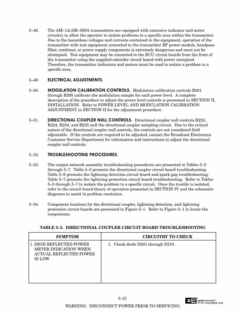
5-21
WARNING: DISCONNECT POWER PRIOR TO SERVICING
5-48. The AM-1A/AM-500A transmitters are equipped with extensive indicator and meter
circuitry to allow the operator to isolate problems to a specific area within the transmitter.
Due to the hazardous voltages and currents contained in the equipment, operation of the
transmitter with test equipment connected to the transmitter RF power module, bandpass
filter, combiner, or power supply components is extremely dangerous and must not be
attempted. Test equipment may be connected to the ECU circuit boards from the front of
the transmitter using the supplied extender circuit board with power energized.
Therefore, the transmitter indicators and meters must be used to isolate a problem to a
specific area.
5-49. ELECTRICAL ADJUSTMENTS.
5-50. MODULATION CALIBRATION CONTROLS. Modulation calibration controls R201
through R205 calibrate the modulation sample for each power level. A complete
description of the procedure to adjust the power level controls is presented in SECTION II,
INSTALLATION. Refer to POWER LEVEL AND MODULATION CALIBRATION
ADJUSTMENT in SECTION II for the adjustment procedure.
5-51. DIRECTIONAL COUPLER NULL CONTROLS. Directional coupler null controls R223,
R224, R234, and R235 null the directional coupler sampling circuit. Due to the critical
nature of the directional coupler null controls, the controls are not considered field
adjustable. If the controls are required to be adjusted, contact the Broadcast Electronics
Customer Service Department for information and instructions to adjust the directional
coupler null controls.
5-52. TROUBLESHOOTING PROCEDURES.
5-53. The output network assembly troubleshooting procedures are presented in Tables 5-5
through 5-7. Table 5-5 presents the directional coupler circuit board troubleshooting.
Table 5-6 presents the lightning detection circuit board and spark gap troubleshooting.
Table 5-7 presents the lightning protection circuit board troubleshooting. Refer to Tables
5-5 through 5-7 to isolate the problem to a specific circuit. Once the trouble is isolated,
refer to the circuit board theory of operation presented in SECTION IV and the schematic
diagrams to assist in problem resolution.
5-54. Component locations for the directional coupler, lightning detection, and lightning
protection circuit boards are presented in Figure 5-1. Refer to Figure 5-1 to locate the
components.
TABLE 5-5. DIRECTIONAL COUPLER CIRCUIT BOARD TROUBLESHOOTING
SYMPTOM CIRCUITRY TO CHECK
1. HIGH REFLECTED POWER 1. Check diode D201 through D210.
METER INDICATION WHEN
ACTUAL REFLECTED POWER
IS LOW
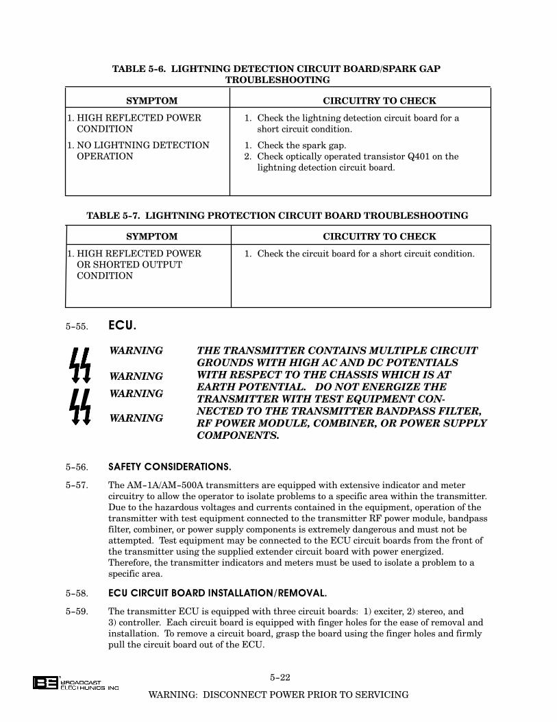
5-22
WARNING: DISCONNECT POWER PRIOR TO SERVICING
TABLE 5-6. LIGHTNING DETECTION CIRCUIT BOARD/SPARK GAP
TROUBLESHOOTING
SYMPTOM CIRCUITRY TO CHECK
1. HIGH REFLECTED POWER 1. Check the lightning detection circuit board for a
CONDITION short circuit condition.
1. NO LIGHTNING DETECTION 1. Check the spark gap.
OPERATION 2. Check optically operated transistor Q401 on the
lightning detection circuit board.
TABLE 5-7. LIGHTNING PROTECTION CIRCUIT BOARD TROUBLESHOOTING
SYMPTOM CIRCUITRY TO CHECK
1. HIGH REFLECTED POWER 1. Check the circuit board for a short circuit condition.
OR SHORTED OUTPUT
CONDITION
5-55. ECU.
WARNING
WARNING
WARNING
WARNING
THE TRANSMITTER CONTAINS MULTIPLE CIRCUIT
GROUNDS WITH HIGH AC AND DC POTENTIALS
WITH RESPECT TO THE CHASSIS WHICH IS AT
EARTH POTENTIAL. DO NOT ENERGIZE THE
TRANSMITTER WITH TEST EQUIPMENT CON�
NECTED TO THE TRANSMITTER BANDPASS FILTER,
RF POWER MODULE, COMBINER, OR POWER SUPPLY
COMPONENTS.
5-56. SAFETY CONSIDERATIONS.
5-57. The AM-1A/AM-500A transmitters are equipped with extensive indicator and meter
circuitry to allow the operator to isolate problems to a specific area within the transmitter.
Due to the hazardous voltages and currents contained in the equipment, operation of the
transmitter with test equipment connected to the transmitter RF power module, bandpass
filter, combiner, or power supply components is extremely dangerous and must not be
attempted. Test equipment may be connected to the ECU circuit boards from the front of
the transmitter using the supplied extender circuit board with power energized.
Therefore, the transmitter indicators and meters must be used to isolate a problem to a
specific area.
5-58. ECU CIRCUIT BOARD INSTALLATION/REMOVAL.
5-59. The transmitter ECU is equipped with three circuit boards: 1) exciter, 2) stereo, and
3) controller. Each circuit board is equipped with finger holes for the ease of removal and
installation. To remove a circuit board, grasp the board using the finger holes and firmly
pull the circuit board out of the ECU.
5-23
WARNING: DISCONNECT POWER PRIOR TO SERVICING
CAUTION
CAUTION
THE TRANSMITTER MAY BE DAMAGED IF THE ECU CIRCUIT BOARDS ARE NOT SECURELY SEATED INTOTHE CONNECTORS.
5-60. To install the circuit boards: 1) the boards must be inserted into the proper location in the
ECU and 2) the boards must be firmly seated into the ECU motherboard. To install a
circuit board, proceed as follows:
1. Refer to Figure 5-2 to determine the circuit board location.
2. Insert the circuit board in the appropriate location.
3. Firmly press the circuit board into the connector to engage the connector
housing.
4. Firmly press the circuit board into the connector again to engage the
connector pins.
5. Repeat the procedure for each ECU circuit board.
5-61. ELECTRICAL ADJUSTMENTS.
5-62. The following text provides electrical adjustment procedures for the transmitter ECU. The
procedures are presented in the following order.
1. ECU Extender Circuit Board Operation.
2. Controller Circuit Board Adjustments.
3. ECU Meter Switch Circuit Board Adjustments.
4. Stereo Circuit Board Adjustments.
5. Exciter Circuit Board Adjustments.
6. Display Circuit Board Adjustments.
5-63. ECU EXTENDER CIRCUIT BOARD OPERATION.
5-64. The transmitter ECU chassis is equipped with an extender circuit board. The circuit board
is designed to allow access to the ECU circuit board components for maintenance
procedures. To use the circuit board for maintenance procedures, proceed as follows:
1. Refer to Figure 5-2 and locate the extender circuit board assembly in the
ECU.
2. Remove the extender circuit board from the ECU.
3. Loosen the extender circuit board locking nut.
4. Completely extend the circuit board.
5. Tighten the extender circuit board locking nut.
6. Remove the circuit board required for maintenance and place the extender
circuit board in the location in the ECU.
7. Place the desired circuit board onto the extender circuit board.
8. Firmly press the circuit board into the extender circuit board connectors.
5-65. CONTROLLER CIRCUIT BOARD ADJUSTMENTS.
5-66. P1 SET - P5 SET CONTROLS. The P1 SET through P5 SET controls adjust the ECU
POWER CONTROL 1 through 5 controls to desired levels. A complete description of the
procedure to adjust the power level controls is presented in SECTION II, INSTALLATION.
Refer to POWER LEVEL AND MODULATION CALIBRATION ADJUSTMENT in
SECTION II for the adjustment procedure.

5-24
WARNING: DISCONNECT POWER PRIOR TO SERVICING
5-67. FWD AND RFL CALIBRATIONS. FWD CAL control R56 and RFL CAL control R143
calibrate the transmitter forward and reflected power samples. Due to the critical nature
of the FWD CAL and RFL CAL controls, the controls are not considered field adjustable. If
the controls are required to be adjusted, contact the Broadcast Electronics Customer
Service Department for information and instructions to adjust the FWD and RFL CAL
controls.
5-68. ECU METER SWITCH CIRCUIT BOARD ADJUSTMENTS.
5-69. FORWARD POWER METER LOW AND HIGH SCALE CALIBRATIONS. Low scale control
R501 and high scale control R504 calibrate the forward power meter. Due to the critical
nature of the low scale and high scale meter calibrate controls, the controls are not
considered field adjustable. If the controls are required to be adjusted, contact the
Broadcast Electronics RF Customer Service Department for information and instructions
to adjust the low and high scale forward power meter controls.
5-70. REFLECTED POWER METER LOW AND HIGH SCALE CALIBRATIONS. Low scale control
R505, high scale control R506, and ac sample control R511 calibrate the reflected power
meter. Due to the critical nature of the low scale, high scale, and ac sample meter
calibrate controls, the controls are not considered field adjustable. If the controls are
required to be adjusted, contact the Broadcast Electronics RF Customer Service
Department for information and instructions to adjust the low scale, high scale, and ac
sample reflected power meter controls.
5-71. FWD AND RFL CALIBRATIONS. FWD CAL control R56 and RFL CAL control R143
calibrate the transmitter forward and reflected power samples. Due to the critical nature
of the FWD CAL and RFL CAL controls, the controls are not considered field adjustable. If
the controls are required to be adjusted, contact the Broadcast Electronics RF Customer
Service Department for information and instructions to adjust the FWD and RFL CAL
controls.
5-72. STEREO CIRCUIT BOARD ADJUSTMENTS.
5-73. STEREO ADJUSTMENT. The stereo adjustment consists of configuring the equalization
circuitry on the stereo circuit board to obtain the optimum stereo performance. The
equalization circuitry consists of the equalization circuit 1 and equalization circuit 2
controls. A complete description of the procedure to adjust the equalization controls is
presented in SECTION II, INSTALLATION. Refer to STEREO ADJUSTMENT in
SECTION II for the adjustment procedure.
5-74. EXCITER CIRCUIT BOARD ADJUSTMENTS.
5-75. MODULATION CALIBRATION. Modulation calibration control R62 calibrates the exciter
modulation circuit. Due to the critical nature of the modulation calibration control, the
control is not considered field adjustable. If the control is to be adjusted, contact the
Broadcast Electronics RF Customer Service Department for information and instructions
to adjust the modulation calibration control.
5-76. PHASE MODULATOR CALIBRATION. Phase modulator calibration control R159
calibrates the exciter phase modulator circuit. Due to the critical nature of the phase
modulator calibration control, the control is not considered field adjustable. If the control
is to be adjusted, contact the Broadcast Electronics RF Customer Service Department for
information and instructions to adjust the phase modulator calibration control.
5-77. SYMMETRY CONTROL. Symmetry calibration control R170 adjusts the exciter RF output
square-wave signal. Due to the critical nature of the symmetry control, the control is not
considered field adjustable. If the control is to be adjusted, contact the Broadcast
Electronics RF Customer Service Department for information and instructions to adjust
the symmetry control.

5-25
WARNING: DISCONNECT POWER PRIOR TO SERVICING
5-78. IPM CORRECTION CIRCUIT CONTROLS. IPM GAIN control R189, IPM TRACK control
R104, IPM SHAPE CONTROL R198, and IPM ZERO SET control R191 calibrate the IPM
correction circuit. Due to the critical nature of the IPM correction circuit controls, the
controls are not considered field adjustable. If the controls are to be adjusted, contact the
Broadcast Electronics RF Customer Service Department for information and instructions
to adjust the IPM correction circuit controls.
5-79. SINGLE CHAN MONO LEVEL CONTROL. SINGLE CHAN MONO LEVEL control R41 is
designed to boost a remaining audio channel level in the event of a failure in one channel.
A complete description of the procedure to adjust the SINGLE CHAN MONO LEVEL
control is presented in SECTION II, INSTALLATION. Refer to SINGLE CHANNEL
LEVEL in SECTION II for the adjustment procedure.
5-80. AVERAGE MODULATION LIMIT CONTROL. Average modulation limit control R217
limits the average tone modulation. The control is adjusted to limit at 110% tone
modulation. Due to the critical nature of the modulation calibration control, the control is
not considered field adjustable. If the control is to be adjusted, contact the Broadcast
Electronics Customer Service Department for information and instructions to adjust the
average modulation limit control.
5-81. NEG LIMIT CONTROL. NEG LIMIT control R76 limits the negative L+R information to
prevent excessive modulation when the L+R signal is summed with the pilot tone. The
NEG LIMIT control is adjusted in the following procedure.
5-82. Procedure. To adjust NEG LIMIT control R76, proceed as follows:
WARNING
WARNING
DISCONNECT ALL TRANSMITTER PRIMARY POWER
BEFORE PROCEEDING.
5-83. Disconnect all transmitter primary power.
5-84. Connect the audio generator to the TB2 LEFT INPUT and RIGHT INPUT audio terminals
on the ECU rear-panel.
5-85. Refer to Figure 5-3 and adjust NEG LIMIT control R76 fully counterclockwise.
5-86. Adjust the audio generator for a L=R 1 kHz output at +10 dBm.
5-87. Adjust the AM stereo modulation monitor to indicate positive L+R modulation.
5-88. Energize the transmitter primary power and operate the transmitter.
5-89. Observe the modulation monitor and ensure the monitor indicates 100% positive L+R
modulation. If the monitor does not indicate 100% L+R modulation, adjust the audio
generator level slightly for a +100% L+R modulation indication on the monitor.
5-90. Adjust the AM stereo modulation monitor to indicate negative L+R modulation.
5-91. Refer to Figure 5-3 and adjust NEG LIMIT control R76 until the AM stereo Modulation
monitor indicates -95% L+R modulation.
WARNING
WARNING
DISCONNECT ALL TRANSMITTER PRIMARY POWER
BEFORE PROCEEDING.
5-92. Disconnect all transmitter primary power.
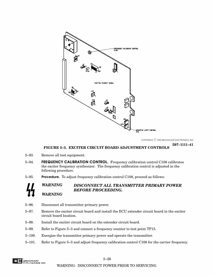
5-26
WARNING: DISCONNECT POWER PRIOR TO SERVICING
COPYRIGHT 1993 BROADCAST ELECTRONICS, INC
597-1111-41FIGURE 5-3. EXCITER CIRCUIT BOARD ADJUSTMENT CONTROLS
5-93. Remove all test equipment.
5-94. FREQUENCY CALIBRATION CONTROL. Frequency calibration control C108 calibrates
the exciter frequency synthesizer. The frequency calibration control is adjusted in the
following procedure.
5-95. Procedure. To adjust frequency calibration control C108, proceed as follows:
WARNING
WARNING
DISCONNECT ALL TRANSMITTER PRIMARY POWER
BEFORE PROCEEDING.
5-96. Disconnect all transmitter primary power.
5-97. Remove the exciter circuit board and install the ECU extender circuit board in the exciter
circuit board location.
5-98. Install the exciter circuit board on the extender circuit board.
5-99. Refer to Figure 5-3 and connect a frequency counter to test point TP15.
5-100. Energize the transmitter primary power and operate the transmitter.
5-101. Refer to Figure 5-3 and adjust frequency calibration control C108 for the carrier frequency.

5-27
WARNING: DISCONNECT POWER PRIOR TO SERVICING
WARNING
WARNING
DISCONNECT ALL TRANSMITTER PRIMARY POWER
BEFORE PROCEEDING.
5-102. Disconnect all transmitter primary power.
5-103. Remove all test equipment and replace the exciter circuit board.
5-104. DISPLAY CIRCUIT BOARD ADJUSTMENTS.
5-105. L/L+R AND R/L-R DISPLAY CALIBRATION CONTROL. L/L+R calibration control R41
and R/L-R calibration control R47 calibrate the L/L+R and R/L-R displays. The L/L+R
and R/L-R calibration controls are adjusted in the following procedure.
5-106. Procedure. To adjust L/L+R calibration control R41 and R/L-R calibration control R47,proceed as follows:
WARNING
WARNING
DISCONNECT ALL TRANSMITTER PRIMARY POWER
BEFORE PROCEEDING.
5-107. Disconnect all transmitter primary power.
5-108. Connect the audio generator to the TB2 LEFT INPUT and RIGHT INPUT audio terminals
on the ECU rear-panel.
5-109. Operate the transmitter at a normal output power.
5-110. Adjust the audio generator for an in-phase L=R 1 kHz output at a level to generate 100%
L+R modulation as indicated by the modulation monitor.
5-111. Operate the EXCITER MONITOR for L+R/L-R indications.
5-112. Adjust L/L+R calibration control R41 on the display circuit board until the EXCITER
MONITOR just indicates 100% L+R modulation.
5-113. Adjust the audio generator for an out-of-phase L=R 1 kHz output at a level to generate
100% L-R modulation as indicated by the modulation monitor.
5-114. Adjust R/L-R calibration control R47 on the display circuit board until the EXCITER
MONITOR just indicates 100% L-R modulation.
WARNING
WARNING
DISCONNECT ALL TRANSMITTER PRIMARY POWER
BEFORE PROCEEDING.
5-115. Disconnect all transmitter primary power.
5-116. Remove all test equipment.
5-117. TROUBLESHOOTING PROCEDURES.
5-118. The ECU assembly troubleshooting procedures are presented in Tables 5-8 through 5-11.
Table 5-8 presents the exciter circuit board troubleshooting. Table 5-9 presents the stereo
circuit board troubleshooting. Table 5-10 presents the controller circuit board
troubleshooting. Table 5-11 presents the ECU power supply troubleshooting. Refer to
Tables 5-8 through 5-11 to isolate the problem to a specific circuit. Once the trouble is
isolated, refer to the circuit board theory of operation in SECTION IV and the schematic
diagrams to assist in problem resolution.
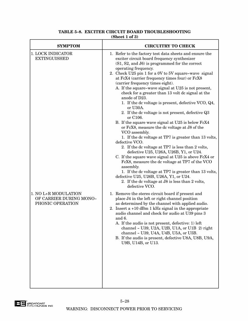
5-28
WARNING: DISCONNECT POWER PRIOR TO SERVICING
TABLE 5-8. EXCITER CIRCUIT BOARD TROUBLESHOOTING
(Sheet 1 of 3)
SYMPTOM CIRCUITRY TO CHECK
1. LOCK INDICATOR 1. Refer to the factory test data sheets and ensure the
EXTINGUISHED exciter circuit board frequency synthesizer
(S1, S2, and J6) is programmed for the correct
operating frequency.
2. Check U25 pin 1 for a 0V to 5V square-wave signal
at FcX4 (carrier frequency times four) or FcX8
(carrier frequency times eight).
A. If the square-wave signal at U25 is not present,
check for a greater than 13 volt dc signal at the
anode of D23.
1. If the dc voltage is present, defective VCO, Q4,
or U30A.
2. If the dc voltage is not present, defective Q3
or C106.
B. If the square wave signal at U25 is below FcX4
or FcX8, measure the dc voltage at J8 of the
VCO assembly.
1. If the dc voltage at TP7 is greater than 13 volts,
defective VCO.
2. If the dc voltage at TP7 is less than 2 volts,
defective U25, U26A, U26B, Y1, or U24.
C. If the square wave signal at U25 is above FcX4 or
FcX8, measure the dc voltage at TP7 of the VCO
assembly.
1. If the dc voltage at TP7 is greater than 13 volts,
defective U25, U26B, U26A, Y1, or U24.
2. If the dc voltage at J8 is less than 2 volts,
defective VCO.
1. NO L+R MODULATION 1. Remove the stereo circuit board if present and
OF CARRIER DURING MONO- place J4 in the left or right channel position
PHONIC OPERATION as determined by the channel with applied audio.
2. Insert a +10 dBm 1 kHz signal in the appropriate
audio channel and check for audio at U39 pins 3
and 6.
A. If the audio is not present, defective: 1) left
channel - U39, U2A, U2B, U1A, or U1B 2) right
channel - U39, U4A, U4B, U5A, or U5B.
B. If the audio is present, defective U8A, U8B, U9A,
U9B, U14B, or U13.
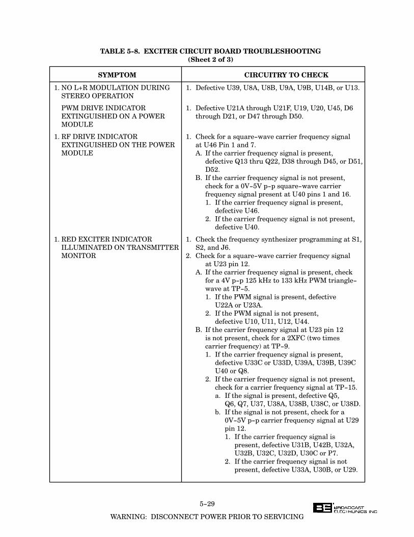
5-29
WARNING: DISCONNECT POWER PRIOR TO SERVICING
TABLE 5-8. EXCITER CIRCUIT BOARD TROUBLESHOOTING
(Sheet 2 of 3)
SYMPTOM CIRCUITRY TO CHECK
1. NO L+R MODULATION DURING 1. Defective U39, U8A, U8B, U9A, U9B, U14B, or U13.
STEREO OPERATION
PWM DRIVE INDICATOR 1. Defective U21A through U21F, U19, U20, U45, D6
EXTINGUISHED ON A POWER through D21, or D47 through D50.
MODULE
1. RF DRIVE INDICATOR 1. Check for a square-wave carrier frequency signal
EXTINGUISHED ON THE POWER at U46 Pin 1 and 7.
MODULE A. If the carrier frequency signal is present,
defective Q13 thru Q22, D38 through D45, or D51,
D52.
B. If the carrier frequency signal is not present,
check for a 0V-5V p-p square-wave carrier
frequency signal present at U40 pins 1 and 16.
1. If the carrier frequency signal is present,
defective U46.
2. If the carrier frequency signal is not present,
defective U40.
1. RED EXCITER INDICATOR 1. Check the frequency synthesizer programming at S1,
ILLUMINATED ON TRANSMITTER S2, and J6.
MONITOR 2. Check for a square-wave carrier frequency signal
at U23 pin 12.
A. If the carrier frequency signal is present, check
for a 4V p-p 125 kHz to 133 kHz PWM triangle-
wave at TP-5.
1. If the PWM signal is present, defective
U22A or U23A.
2. If the PWM signal is not present,
defective U10, U11, U12, U44.
B. If the carrier frequency signal at U23 pin 12
is not present, check for a 2XFC (two times
carrier frequency) at TP-9.
1. If the carrier frequency signal is present,
defective U33C or U33D, U39A, U39B, U39C
U40 or Q8.
2. If the carrier frequency signal is not present,
check for a carrier frequency signal at TP-15.
a. If the signal is present, defective Q5,
Q6, Q7, U37, U38A, U38B, U38C, or U38D.
b. If the signal is not present, check for a
0V-5V p-p carrier frequency signal at U29
pin 12.
1. If the carrier frequency signal is
present, defective U31B, U42B, U32A,
U32B, U32C, U32D, U30C or P7.
2. If the carrier frequency signal is not
present, defective U33A, U30B, or U29.
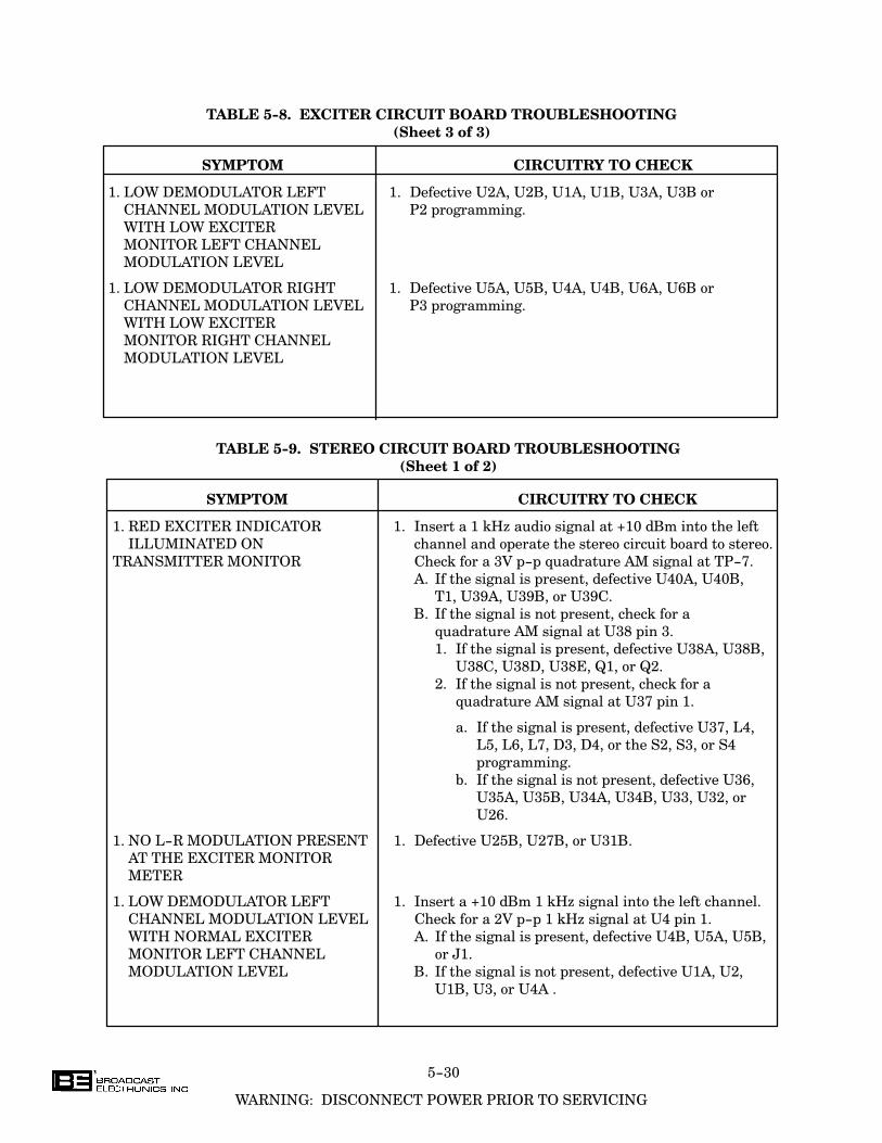
5-30
WARNING: DISCONNECT POWER PRIOR TO SERVICING
TABLE 5-8. EXCITER CIRCUIT BOARD TROUBLESHOOTING
(Sheet 3 of 3)
SYMPTOM CIRCUITRY TO CHECK
1. LOW DEMODULATOR LEFT 1. Defective U2A, U2B, U1A, U1B, U3A, U3B or
CHANNEL MODULATION LEVEL P2 programming.
WITH LOW EXCITER
MONITOR LEFT CHANNEL
MODULATION LEVEL
1. LOW DEMODULATOR RIGHT 1. Defective U5A, U5B, U4A, U4B, U6A, U6B or
CHANNEL MODULATION LEVEL P3 programming.
WITH LOW EXCITER
MONITOR RIGHT CHANNEL
MODULATION LEVEL
TABLE 5-9. STEREO CIRCUIT BOARD TROUBLESHOOTING
(Sheet 1 of 2)
SYMPTOM CIRCUITRY TO CHECK
1. RED EXCITER INDICATOR 1. Insert a 1 kHz audio signal at +10 dBm into the left
ILLUMINATED ON channel and operate the stereo circuit board to stereo.
TRANSMITTER MONITOR Check for a 3V p-p quadrature AM signal at TP-7.
A. If the signal is present, defective U40A, U40B,
T1, U39A, U39B, or U39C.
B. If the signal is not present, check for a
quadrature AM signal at U38 pin 3.
1. If the signal is present, defective U38A, U38B,
U38C, U38D, U38E, Q1, or Q2.
2. If the signal is not present, check for a
quadrature AM signal at U37 pin 1.
a. If the signal is present, defective U37, L4,
L5, L6, L7, D3, D4, or the S2, S3, or S4
programming.
b. If the signal is not present, defective U36,
U35A, U35B, U34A, U34B, U33, U32, or
U26.
1. NO L-R MODULATION PRESENT 1. Defective U25B, U27B, or U31B.
AT THE EXCITER MONITOR
METER
1. LOW DEMODULATOR LEFT 1. Insert a +10 dBm 1 kHz signal into the left channel.
CHANNEL MODULATION LEVEL Check for a 2V p-p 1 kHz signal at U4 pin 1.
WITH NORMAL EXCITER A. If the signal is present, defective U4B, U5A, U5B,
MONITOR LEFT CHANNEL or J1.
MODULATION LEVEL B. If the signal is not present, defective U1A, U2,
U1B, U3, or U4A .
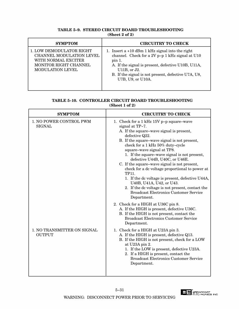
5-31
WARNING: DISCONNECT POWER PRIOR TO SERVICING
TABLE 5-9. STEREO CIRCUIT BOARD TROUBLESHOOTING
(Sheet 2 of 2)
SYMPTOM CIRCUITRY TO CHECK
1. LOW DEMODULATOR RIGHT 1. Insert a +10 dBm 1 kHz signal into the right
CHANNEL MODULATION LEVEL channel. Check for a 2V p-p 1 kHz signal at U10
WITH NORMAL EXCITER pin 1.
MONITOR RIGHT CHANNEL A. If the signal is present, defective U10B, U11A,
MODULATION LEVEL U11B, or J2.
B. If the signal is not present, defective U7A, U8,
U7B, U9, or U10A.
TABLE 5-10. CONTROLLER CIRCUIT BOARD TROUBLESHOOTING
(Sheet 1 of 2)
SYMPTOM CIRCUITRY TO CHECK
1. NO POWER CONTROL PWM 1. Check for a 1 kHz 15V p-p square-wave
SIGNAL signal at TP-7.
A. If the square-wave signal is present,
defective Q22.
B. If the square-wave signal is not present,
check for a 1 kHz 50% duty-cycle
square-wave signal at TP8.
1. If the square-wave signal is not present,
defective U44B, U40C, or U46E.
C. If the square-wave signal is not present,
check for a dc voltage proportional to power at
TP11.
1. If the dc voltage is present, defective U44A,
U40B, U41A, U42, or U43.
2. If the dc voltage is not present, contact the
Broadcast Electronics Customer Service
Department.
2. Check for a HIGH at U36C pin 8.
A. If the HIGH is present, defective U36C.
B. If the HIGH is not present, contact the
Broadcast Electronics Customer Service
Department.
1. NO TRANSMITTER ON SIGNAL 1. Check for a HIGH at U23A pin 3.
OUTPUT A. If the HIGH is present, defective Q13.
B. If the HIGH is not present, check for a LOW
at U23A pin 2.
1. If the LOW is present, defective U23A.
2. If a HIGH is present, contact the
Broadcast Electronics Customer Service
Department.
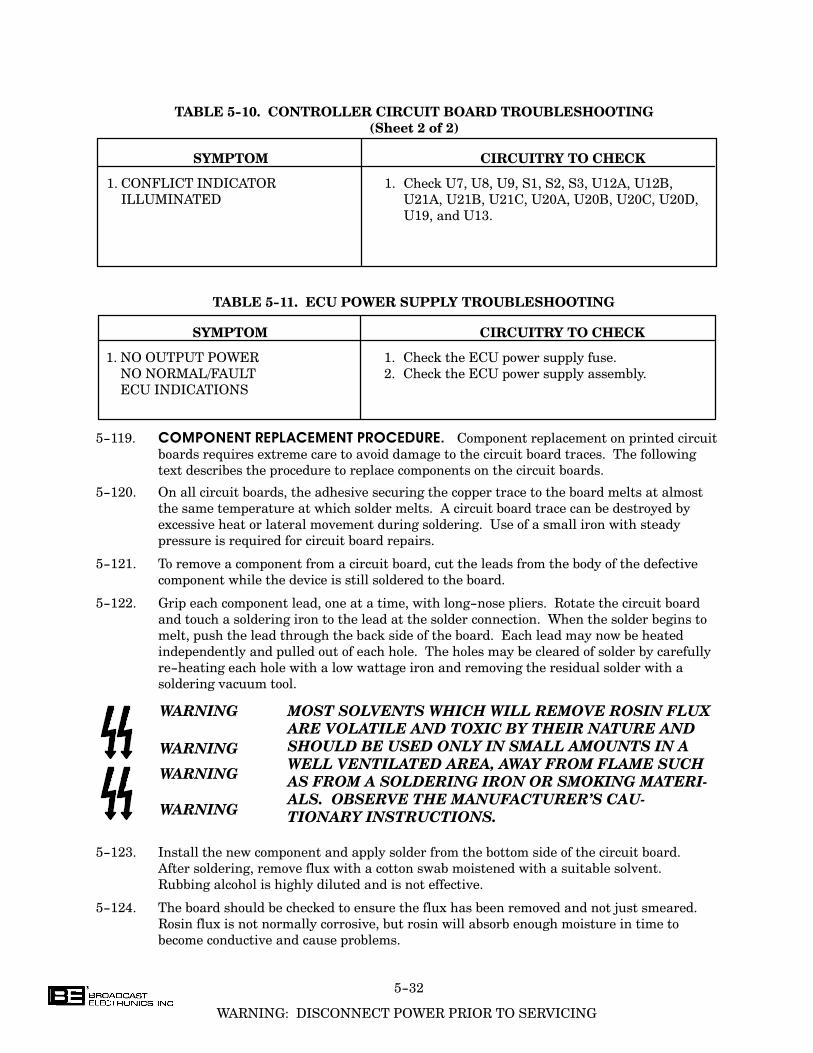
5-32
WARNING: DISCONNECT POWER PRIOR TO SERVICING
TABLE 5-10. CONTROLLER CIRCUIT BOARD TROUBLESHOOTING
(Sheet 2 of 2)
SYMPTOM CIRCUITRY TO CHECK
1. CONFLICT INDICATOR 1. Check U7, U8, U9, S1, S2, S3, U12A, U12B,
ILLUMINATED U21A, U21B, U21C, U20A, U20B, U20C, U20D,
U19, and U13.
TABLE 5-11. ECU POWER SUPPLY TROUBLESHOOTING
SYMPTOM CIRCUITRY TO CHECK
1. NO OUTPUT POWER 1. Check the ECU power supply fuse.
NO NORMAL/FAULT 2. Check the ECU power supply assembly.
ECU INDICATIONS
5-119. COMPONENT REPLACEMENT PROCEDURE. Component replacement on printed circuit
boards requires extreme care to avoid damage to the circuit board traces. The following
text describes the procedure to replace components on the circuit boards.
5-120. On all circuit boards, the adhesive securing the copper trace to the board melts at almost
the same temperature at which solder melts. A circuit board trace can be destroyed by
excessive heat or lateral movement during soldering. Use of a small iron with steady
pressure is required for circuit board repairs.
5-121. To remove a component from a circuit board, cut the leads from the body of the defective
component while the device is still soldered to the board.
5-122. Grip each component lead, one at a time, with long-nose pliers. Rotate the circuit board
and touch a soldering iron to the lead at the solder connection. When the solder begins to
melt, push the lead through the back side of the board. Each lead may now be heated
independently and pulled out of each hole. The holes may be cleared of solder by carefully
re-heating each hole with a low wattage iron and removing the residual solder with a
soldering vacuum tool.
WARNING
WARNING
WARNING
WARNING
MOST SOLVENTS WHICH WILL REMOVE ROSIN FLUX
ARE VOLATILE AND TOXIC BY THEIR NATURE AND
SHOULD BE USED ONLY IN SMALL AMOUNTS IN A
WELL VENTILATED AREA, AWAY FROM FLAME SUCH
AS FROM A SOLDERING IRON OR SMOKING MATERI�
ALS. OBSERVE THE MANUFACTURER'S CAU�
TIONARY INSTRUCTIONS.
5-123. Install the new component and apply solder from the bottom side of the circuit board.
After soldering, remove flux with a cotton swab moistened with a suitable solvent.
Rubbing alcohol is highly diluted and is not effective.
5-124. The board should be checked to ensure the flux has been removed and not just smeared.
Rosin flux is not normally corrosive, but rosin will absorb enough moisture in time to
become conductive and cause problems.
5-33
WARNING: DISCONNECT POWER PRIOR TO SERVICING
5-125. INTEGRATED CIRCUITS. Special care should be exercised with integrated circuits. Each
integrated circuit must be installed by matching the integrated circuit notch with the
notch on the socket. Do not attempt to remove an integrated circuit from a socket with
your fingers. Use an integrated circuit puller to lightly pry the component from the socket.

6-1
SECTION VI
PARTS LIST
6-1. INTRODUCTION.
6-2. This section provides parts lists for the AM-1A/AM-500A transmitters. The parts lists
provide descriptions and part numbers of electrical components, assemblies, and selected
mechanical parts required for maintenance. Each parts list entry in this section is indexed
by reference designators appearing on the applicable schematic diagrams.
TABLE 6-1. AM-1A/AM-500A REPLACEABLE PARTS LIST INDEX
(Sheet 1 of 2)
TABLE DESCRIPTION PART NO. PAGE
6-2 AM-1A Transmitter 907-1000-001 6-3
6-3 AM-500A Transmitter 907-0500-001 6-3
6-4 Exciter/Controller Assembly 957-0009-011 6-3
6-5 ECU Controller Circuit Board Assembly 917-0205 6-4
6-6 ECU Extender Circuit Board Assembly 917-0208 6-13
6-7 Stereo Circuit Board Assembly 917-0209 6-13
6-8 ECU Exciter Circuit Board Assembly 917-0300 6-22
6-9 VCO Module Circuit Board Assembly 917-0069 6-31
6-10 ECU Motherboard Circuit Board Assembly 917-0301 6-31
6-11 ECU Display/Control Switch Circuit Board 917-0306-001 6-33
6-12 Meter Switch Circuit Board Assembly 917-0306-005 6-36
6-13 ECU Wire Harness 947-0153 6-37
6-14 Power Module Assembly 957-0010-001 6-37
6-15 Modulator Circuit Board Assembly 917-0302 6-38
6-16 Power Amplifier Circuit Board Assembly 917-0304 6-41
6-17 Output Network Assembly, AM-1A 957-0064 6-43
Output Network Assembly, AM-500A 957-0064-500
6-18 Power Block Motherboard Circuit Board Assembly 917-0303-001 6-45
6-19 Directional Coupler Circuit Board Assembly 917-0306-002 6-45
6-20 AC Sample Circuit Board Assembly 917-0306-007 6-46
6-21 Temperature Sensor Circuit Board Assembly 917-0306-009 6-47
6-22 Lightning Detector Circuit Board Assembly 917-0306-014 6-47
6-23 Power Supply Circuit Board Assembly 917-0315-001 6-47
6-24 Power Supply Bulk Capacitor Circuit Board Assembly 917-0315-003 6-54
6-25 Power Supply Capacitor Circuit Board Assembly 917-0315-005 6-54
6-26 Lightning Protection Circuit Board Assembly, AM-1A 917-0316 6-55
6-27 Lightning Protection Circuit Board Assembly, AM-500A 917-0216 6-55
6-28 Combiner Circuit Board Assembly 917-0321-001 6-55
6-29 Optically Coupled Relay Circuit Board Assembly 919-0096-001 6-55
6-30 Optically Coupled Relay Circuit Board Assembly 919-0096 6-55
6-31 Wire Harness 947-0179 6-56
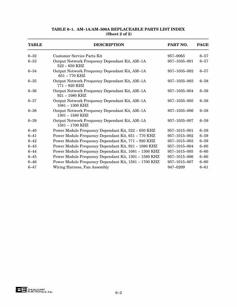
6-2
TABLE 6-1. AM-1A/AM-500A REPLACEABLE PARTS LIST INDEX
(Sheet 2 of 2)
TABLE DESCRIPTION PART NO. PAGE
6-32 Customer Service Parts Kit 957-0065 6-57
6-33 Output Network Frequency Dependant Kit, AM-1A 957-1035-001 6-57
522 - 650 KHZ
6-34 Output Network Frequency Dependant Kit, AM-1A 957-1035-002 6-57
651 - 770 KHZ
6-35 Output Network Frequency Dependant Kit, AM-1A 957-1035-003 6-58
771 - 920 KHZ
6-36 Output Network Frequency Dependant Kit, AM-1A 957-1035-004 6-58
921 - 1080 KHZ
6-37 Output Network Frequency Dependant Kit, AM-1A 957-1035-005 6-58
1081 - 1300 KHZ
6-38 Output Network Frequency Dependant Kit, AM-1A 957-1035-006 6-58
1301 - 1580 KHZ
6-39 Output Network Frequency Dependant Kit, AM-1A 957-1035-007 6-59
1581 - 1700 KHZ
6-40 Power Module Frequency Dependant Kit, 522 - 650 KHZ 957-1015-001 6-59
6-41 Power Module Frequency Dependant Kit, 651 - 770 KHZ 957-1015-002 6-59
6-42 Power Module Frequency Dependant Kit, 771 - 920 KHZ 957-1015-003 6-59
6-43 Power Module Frequency Dependant Kit, 921 - 1080 KHZ 957-1015-004 6-60
6-44 Power Module Frequency Dependant Kit, 1081 - 1300 KHZ 957-1015-005 6-60
6-45 Power Module Frequency Dependant Kit, 1301 - 1580 KHZ 957-1015-006 6-60
6-46 Power Module Frequency Dependant Kit, 1581 - 1700 KHZ 957-1015-007 6-60
6-47 Wiring Harness, Fan Assembly 947-0209 6-61
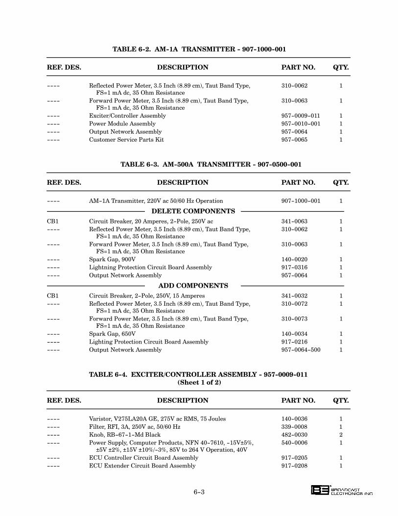
6-3
TABLE 6-2. AM-1A TRANSMITTER - 907-1000-001
REF. DES. DESCRIPTION PART NO. QTY.
---- Reflected Power Meter, 3.5 Inch (8.89 cm), Taut Band Type, 310-0062 1
FS=1 mA dc, 35 Ohm Resistance
---- Forward Power Meter, 3.5 Inch (8.89 cm), Taut Band Type, 310-0063 1
FS=1 mA dc, 35 Ohm Resistance
---- Exciter/Controller Assembly 957-0009-011 1
---- Power Module Assembly 957-0010-001 1
---- Output Network Assembly 957-0064 1
---- Customer Service Parts Kit 957-0065 1
TABLE 6-3. AM-500A TRANSMITTER - 907-0500-001
REF. DES. DESCRIPTION PART NO. QTY.
---- AM-1A Transmitter, 220V ac 50/60 Hz Operation 907-1000-001 1
DELETE COMPONENTS
CB1 Circuit Breaker, 20 Amperes, 2-Pole, 250V ac 341-0063 1
---- Reflected Power Meter, 3.5 Inch (8.89 cm), Taut Band Type, 310-0062 1
FS=1 mA dc, 35 Ohm Resistance
---- Forward Power Meter, 3.5 Inch (8.89 cm), Taut Band Type, 310-0063 1
FS=1 mA dc, 35 Ohm Resistance
---- Spark Gap, 900V 140-0020 1
---- Lightning Protection Circuit Board Assembly 917-0316 1
---- Output Network Assembly 957-0064 1
ADD COMPONENTS
CB1 Circuit Breaker, 2-Pole, 250V, 15 Amperes 341-0032 1
---- Reflected Power Meter, 3.5 Inch (8.89 cm), Taut Band Type, 310-0072 1
FS=1 mA dc, 35 Ohm Resistance
---- Forward Power Meter, 3.5 Inch (8.89 cm), Taut Band Type, 310-0073 1
FS=1 mA dc, 35 Ohm Resistance
---- Spark Gap, 650V 140-0034 1
---- Lighting Protection Circuit Board Assembly 917-0216 1
---- Output Network Assembly 957-0064-500 1
TABLE 6-4. EXCITER/CONTROLLER ASSEMBLY - 957-0009-011
(Sheet 1 of 2)
REF. DES. DESCRIPTION PART NO. QTY.
---- Varistor, V275LA20A GE, 275V ac RMS, 75 Joules 140-0036 1
---- Filter, RFI, 3A, 250V ac, 50/60 Hz 339-0008 1
---- Knob, RB-67-1-Md Black 482-0030 2
---- Power Supply, Computer Products, NFN 40-7610, -15V±5%, 540-0006 1
±5V ±2%, ±15V ±10%/-3%, 85V to 264 V Operation, 40V
---- ECU Controller Circuit Board Assembly 917-0205 1
---- ECU Extender Circuit Board Assembly 917-0208 1
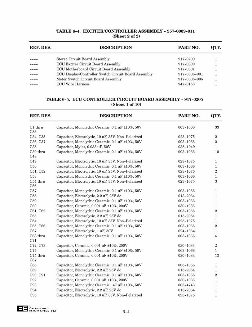
6-4
TABLE 6-4. EXCITER/CONTROLLER ASSEMBLY - 957-0009-011
(Sheet 2 of 2)
REF. DES. DESCRIPTION PART NO. QTY.
---- Stereo Circuit Board Assembly 917-0209 1
---- ECU Exciter Circuit Board Assembly 917-0300 1
---- ECU Motherboard Circuit Board Assembly 917-0301 1
---- ECU Display/Controller Switch Circuit Board Assembly 917-0306-001 1
---- Meter Switch Circuit Board Assembly 917-0306-005 1
---- ECU Wire Harness 947-0153 1
TABLE 6-5. ECU CONTROLLER CIRCUIT BOARD ASSEMBLY - 917-0205
(Sheet 1 of 10)
REF. DES. DESCRIPTION PART NO. QTY.
C1 thru Capacitor, Monolythic Ceramic, 0.1 uF ±10%, 50V 003-1066 33
C33
C34, C35 Capacitor, Electrolytic, 10 uF, 35V, Non-Polarized 023-1075 2
C36, C37 Capacitor, Monolythic Ceramic, 0.1 uF ±10%, 50V 003-1066 2
C38 Capacitor, Mylar, 0.033 uF, 50V 038-1049 1
C39 thru Capacitor, Monolythic Ceramic, 0.1 uF ±10%, 50V 003-1066 10
C48
C49 Capacitor, Electrolytic, 10 uF, 35V, Non-Polarized 023-1075 1
C50 Capacitor, Monolythic Ceramic, 0.1 uF ±10%, 50V 003-1066 1
C51, C52 Capacitor, Electrolytic, 10 uF, 25V, Non-Polarized 023-1075 2
C53 Capacitor, Monolythic Ceramic, 0.1 uF ±10%, 50V 003-1066 1
C54 thru Capacitor, Electrolytic, 10 uF, 35V, Non-Polarized 023-1075 3
C56
C57 Capacitor, Monolythic Ceramic, 0.1 uF ±10%, 50V 003-1066 1
C58 Capacitor, Electrolytic, 2.2 uF, 25V dc 013-2064 1
C59 Capacitor, Monolythic Ceramic, 0.1 uF ±10%, 50V 003-1066 1
C60 Capacitor, Ceramic, 0.001 uF ±10%, 200V 030-1033 1
C61, C62 Capacitor, Monolythic Ceramic, 0.1 uF ±10%, 50V 003-1066 2
C63 Capacitor, Electrolytic, 2.2 uF, 25V dc 013-2064 1
C64 Capacitor, Electrolytic, 10 uF, 35V, Non-Polarized 023-1075 1
C65, C66 Capacitor, Monolythic Ceramic, 0.1 uF ±10%, 50V 003-1066 2
C67 Capacitor, Electrolytic, 1 uF, 50V 024-1064 1
C68 thru Capacitor, Monolythic Ceramic, 0.1 uF ±10%, 50V 003-1066 4
C71
C72, C73 Capacitor, Ceramic, 0.001 uF ±10%, 200V 030-1033 2
C74 Capacitor, Monolythic Ceramic, 0.1 uF ±10%, 50V 003-1066 1
C75 thru Capacitor, Ceramic, 0.001 uF ±10%, 200V 030-1033 13
C87
C88 Capacitor, Monolythic Ceramic, 0.1 uF ±10%, 50V 003-1066 1
C89 Capacitor, Electrolytic, 2.2 uF, 25V dc 013-2064 1
C90, C91 Capacitor, Monolythic Ceramic, 0.1 uF ±10%, 50V 003-1066 2
C92 Capacitor, Ceramic, 0.001 uF ±10%, 200V 030-1033 1
C93 Capacitor, Monolythic Ceramic, .47 uF ±10%, 50V 003-4743 1
C94 Capacitor, Electrolytic, 2.2 uF, 25V dc 013-2064 1
C95 Capacitor, Electrolytic, 10 uF, 35V, Non-Polarized 023-1075 1
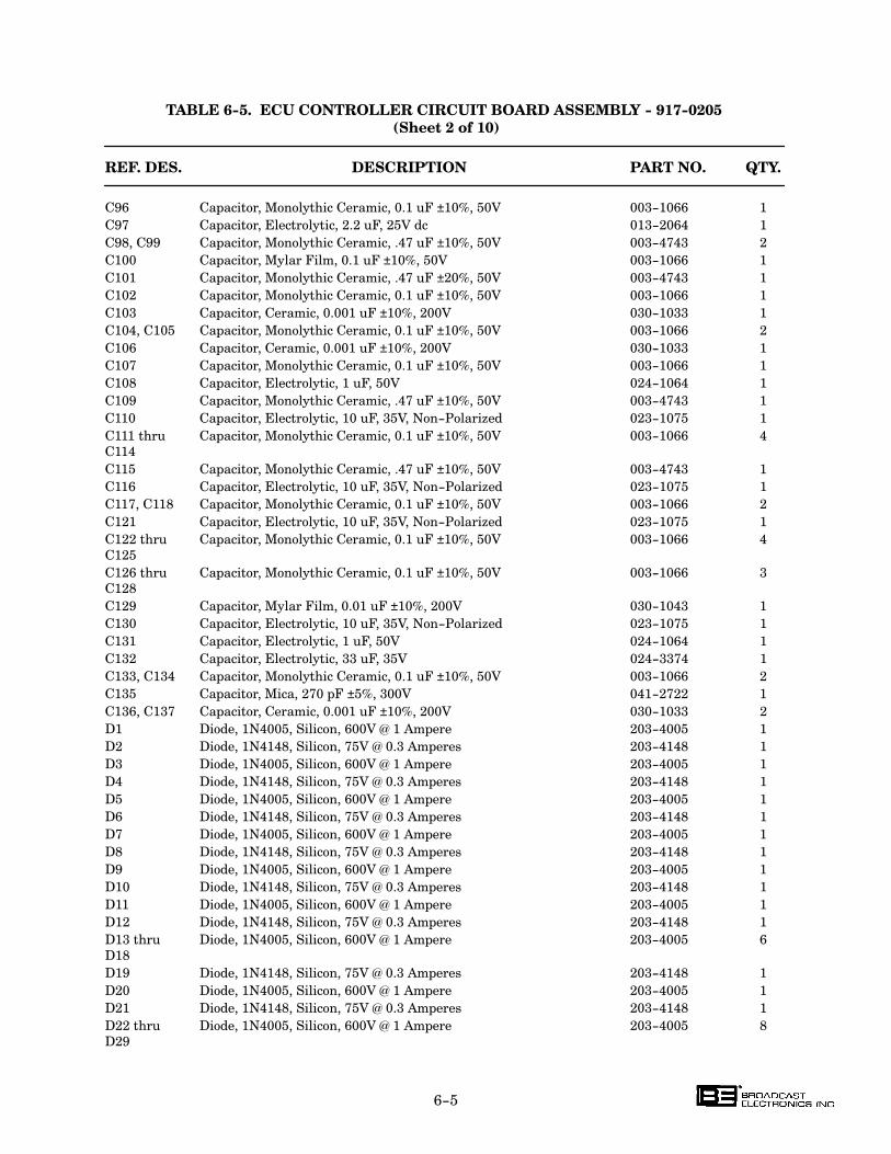
6-5
TABLE 6-5. ECU CONTROLLER CIRCUIT BOARD ASSEMBLY - 917-0205
(Sheet 2 of 10)
REF. DES. DESCRIPTION PART NO. QTY.
C96 Capacitor, Monolythic Ceramic, 0.1 uF ±10%, 50V 003-1066 1
C97 Capacitor, Electrolytic, 2.2 uF, 25V dc 013-2064 1
C98, C99 Capacitor, Monolythic Ceramic, .47 uF ±10%, 50V 003-4743 2
C100 Capacitor, Mylar Film, 0.1 uF ±10%, 50V 003-1066 1
C101 Capacitor, Monolythic Ceramic, .47 uF ±20%, 50V 003-4743 1
C102 Capacitor, Monolythic Ceramic, 0.1 uF ±10%, 50V 003-1066 1
C103 Capacitor, Ceramic, 0.001 uF ±10%, 200V 030-1033 1
C104, C105 Capacitor, Monolythic Ceramic, 0.1 uF ±10%, 50V 003-1066 2
C106 Capacitor, Ceramic, 0.001 uF ±10%, 200V 030-1033 1
C107 Capacitor, Monolythic Ceramic, 0.1 uF ±10%, 50V 003-1066 1
C108 Capacitor, Electrolytic, 1 uF, 50V 024-1064 1
C109 Capacitor, Monolythic Ceramic, .47 uF ±10%, 50V 003-4743 1
C110 Capacitor, Electrolytic, 10 uF, 35V, Non-Polarized 023-1075 1
C111 thru Capacitor, Monolythic Ceramic, 0.1 uF ±10%, 50V 003-1066 4
C114
C115 Capacitor, Monolythic Ceramic, .47 uF ±10%, 50V 003-4743 1
C116 Capacitor, Electrolytic, 10 uF, 35V, Non-Polarized 023-1075 1
C117, C118 Capacitor, Monolythic Ceramic, 0.1 uF ±10%, 50V 003-1066 2
C121 Capacitor, Electrolytic, 10 uF, 35V, Non-Polarized 023-1075 1
C122 thru Capacitor, Monolythic Ceramic, 0.1 uF ±10%, 50V 003-1066 4
C125
C126 thru Capacitor, Monolythic Ceramic, 0.1 uF ±10%, 50V 003-1066 3
C128
C129 Capacitor, Mylar Film, 0.01 uF ±10%, 200V 030-1043 1
C130 Capacitor, Electrolytic, 10 uF, 35V, Non-Polarized 023-1075 1
C131 Capacitor, Electrolytic, 1 uF, 50V 024-1064 1
C132 Capacitor, Electrolytic, 33 uF, 35V 024-3374 1
C133, C134 Capacitor, Monolythic Ceramic, 0.1 uF ±10%, 50V 003-1066 2
C135 Capacitor, Mica, 270 pF ±5%, 300V 041-2722 1
C136, C137 Capacitor, Ceramic, 0.001 uF ±10%, 200V 030-1033 2
D1 Diode, 1N4005, Silicon, 600V @ 1 Ampere 203-4005 1
D2 Diode, 1N4148, Silicon, 75V @ 0.3 Amperes 203-4148 1
D3 Diode, 1N4005, Silicon, 600V @ 1 Ampere 203-4005 1
D4 Diode, 1N4148, Silicon, 75V @ 0.3 Amperes 203-4148 1
D5 Diode, 1N4005, Silicon, 600V @ 1 Ampere 203-4005 1
D6 Diode, 1N4148, Silicon, 75V @ 0.3 Amperes 203-4148 1
D7 Diode, 1N4005, Silicon, 600V @ 1 Ampere 203-4005 1
D8 Diode, 1N4148, Silicon, 75V @ 0.3 Amperes 203-4148 1
D9 Diode, 1N4005, Silicon, 600V @ 1 Ampere 203-4005 1
D10 Diode, 1N4148, Silicon, 75V @ 0.3 Amperes 203-4148 1
D11 Diode, 1N4005, Silicon, 600V @ 1 Ampere 203-4005 1
D12 Diode, 1N4148, Silicon, 75V @ 0.3 Amperes 203-4148 1
D13 thru Diode, 1N4005, Silicon, 600V @ 1 Ampere 203-4005 6
D18
D19 Diode, 1N4148, Silicon, 75V @ 0.3 Amperes 203-4148 1
D20 Diode, 1N4005, Silicon, 600V @ 1 Ampere 203-4005 1
D21 Diode, 1N4148, Silicon, 75V @ 0.3 Amperes 203-4148 1
D22 thru Diode, 1N4005, Silicon, 600V @ 1 Ampere 203-4005 8
D29
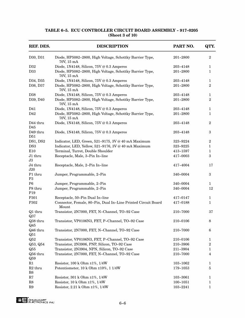
6-6
TABLE 6-5. ECU CONTROLLER CIRCUIT BOARD ASSEMBLY - 917-0205
(Sheet 3 of 10)
REF. DES. DESCRIPTION PART NO. QTY.
D30, D31 Diode, HP5082-2800, High Voltage, Schottky Barrier Type, 201-2800 2
70V, 15 mA
D32 Diode, 1N4148, Silicon, 75V @ 0.3 Amperes 203-4148 1
D33 Diode, HP5082-2800, High Voltage, Schottky Barrier Type, 201-2800 1
70V, 15 mA
D34, D35 Diode, 1N4148, Silicon, 75V @ 0.3 Amperes 203-4148 1
D36, D37 Diode, HP5082-2800, High Voltage, Schottky Barrier Type, 201-2800 2
70V, 15 mA
D38 Diode, 1N4148, Silicon, 75V @ 0.3 Amperes 203-4148 1
D39, D40 Diode, HP5082-2800, High Voltage, Schottky Barrier Type, 201-2800 2
70V, 15 mA
D41 Diode, 1N4148, Silicon, 75V @ 0.3 Amperes 203-4148 1
D42 Diode, HP5082-2800, High Voltage, Schottky Barrier Type, 201-2800 1
70V, 15 mA
D44 thru Diode, 1N4148, Silicon, 75V @ 0.3 Amperes 203-4148 2
D45
D49 thru Diode, 1N4148, Silicon, 75V @ 0.3 Amperes 203-4148 3
D51
DS1, DS2 Indicator, LED, Green, 521-9175, 3V @ 40 mA Maximum 323-9224 2
DS3 Indicator, LED, Yellow, 521-9176, 3V @ 40 mA Maximum 323-9225 1
E10 Terminal, Turret, Double Shoulder 413-1597 1
J1 thru Receptacle, Male, 3-Pin In-line 417-0003 3
J3
J4 thru Receptacle, Male, 2-Pin In-line 417-4004 17
J20
P1 thru Jumper, Programmable, 2-Pin 340-0004 3
P3
P6 Jumper, Programmable, 2-Pin 340-0004 1
P8 thru Jumper, Programmable, 2-Pin 340-0004 12
P19
P301 Receptacle, 50-Pin Dual In-line 417-0147 1
P302 Connector, Female, 80-Pin, Dual In-Line Printed Circuit Board 417-0188 1
Mount
Q1 thru Transistor, 2N7000, FET, N-Channel, TO-92 Case 210-7000 37
Q37
Q38 thru Transistor, VP0106N3, FET, P-Channel, TO-92 Case 210-0106 8
Q45
Q46 thru Transistor, 2N7000, FET, N-Channel, TO-92 Case 210-7000 6
Q51
Q52 Transistor, VP0106N3, FET, P-Channel, TO-92 Case 210-0106 1
Q53, Q54 Transistor, 2N3906, PNP, Silicon, TO-92 Case 210-3906 2
Q55 Transistor, 2N3904, NPN, Silicon, TO-92 Case 211-3904 1
Q56 thru Transistor, 2N7000, FET, N-Channel, TO-92 Case 210-7000 4
Q59
R1 Resistor, 100 k Ohm ±1%, 1/4W 103-1062 1
R2 thru Potentiometer, 10 k Ohm ±10%, 1 1/4W 179-1053 5
R6
R7 Resistor, 301 k Ohm ±1%, 1/4W 103-3061 1
R8 Resistor, 10 k Ohm ±1%, 1/4W 100-1051 1
R9 Resistor, 2.21 k Ohm ±1%, 1/4W 103-2241 1
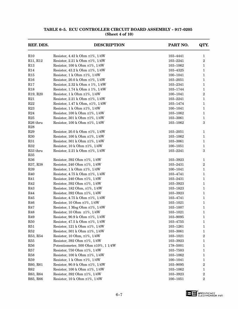
6-7
TABLE 6-5. ECU CONTROLLER CIRCUIT BOARD ASSEMBLY - 917-0205
(Sheet 4 of 10)
REF. DES. DESCRIPTION PART NO. QTY.
R10 Resistor, 4.42 k Ohm ±1%, 1/4W 103-4441 1
R11, R12 Resistor, 2.21 k Ohm ±1%, 1/4W 103-2241 2
R13 Resistor, 100 k Ohm ±1%, 1/4W 103-1062 1
R14 Resistor, 43.2 k Ohm ±1%, 1/4W 103-4325 1
R15 Resistor, 1 k Ohm ±1%, 1/4W 100-1041 1
R16 Resistor, 20.0 k Ohm ±1%, 1/4W 103-2051 1
R17 Resistor, 2.32 k Ohm ± 1%, 1/4W 103-2341 1
R18 Resistor, 1.74 k Ohm ± 1%, 1/4W 103-1744 1
R19, R20 Resistor, 1 k Ohm ±1%, 1/4W 100-1041 2
R21 Resistor, 2.21 k Ohm ±1%, 1/4W 103-2241 1
R22 Resistor, 1.47 k Ohm, ±1%, 1/4W 103-1474 1
R23 Resistor, 1 k Ohm ±1%, 1/4W 100-1041 1
R24 Resistor, 100 k Ohm ±1%, 1/4W 103-1062 1
R25 Resistor, 301 k Ohm ±1%, 1/4W 103-3061 1
R26 thru Resistor, 100 k Ohm ±1%, 1/4W 103-1062 3
R28
R29 Resistor, 20.0 k Ohm ±1%, 1/4W 103-2051 1
R30 Resistor, 100 k Ohm ±1%, 1/4W 103-1062 1
R31 Resistor, 301 k Ohm ±1%, 1/4W 103-3061 1
R32 Resistor, 10 k Ohm ±1%, 1/4W 100-1051 1
R33 thru Resistor, 2.21 k Ohm ±1%, 1/4W 103-2241 3
R35
R36 Resistor, 392 Ohm ±1%, 1/4W 103-3923 1
R37, R38 Resistor, 240 Ohm ±1%, 1/4W 103-2431 2
R39 Resistor, 1 k Ohm ±1%, 1/4W 100-1041 1
R40 Resistor, 4.75 k Ohm ±1%, 1/4W 103-4741 1
R41 Resistor, 240 Ohm ±1%, 1/4W 103-2431 1
R42 Resistor, 392 Ohm ±1%, 1/4W 103-3923 1
R43 Resistor, 182 Ohm, ±1%, 1/4W 103-1823 1
R44 Resistor, 392 Ohm ±1%, 1/4W 103-3923 1
R45 Resistor, 4.75 k Ohm ±1%, 1/4W 103-4741 1
R46 Resistor, 10 Ohm ±1%, 1/4W 103-1021 1
R47 Resistor, 1 Meg Ohm ±1%, 1/4W 103-1007 1
R48 Resistor, 10 Ohm ±1%, 1/4W 103-1021 1
R49 Resistor, 90.9 k Ohm ±1%, 1/4W 103-9095 1
R50 Resistor, 47.5 k Ohm ±1%, 1/4W 103-4755 1
R51 Resistor, 121 k Ohm ±1%, 1/4W 103-1261 1
R52 Resistor, 301 k Ohm ±1%, 1/4W 103-3061 1
R53, R54 Resistor, 10 Ohm, ±1%, 1/4W 103-1021 2
R55 Resistor, 392 Ohm ±1%, 1/4W 103-3923 1
R56 Potentiometer, 500 Ohm ±10%, 1 1/4W 178-5001 1
R57 Resistor, 750 Ohm ±1%, 1/4W 103-7503 1
R58 Resistor, 100 k Ohm ±1%, 1/4W 103-1062 1
R59 Resistor, 1 k Ohm ±1%, 1/4W 100-1041 1
R60, R61 Resistor, 90.9 k Ohm ±1%, 1/4W 103-9095 2
R62 Resistor, 100 k Ohm ±1%, 1/4W 103-1062 1
R63, R64 Resistor, 392 Ohm ±1%, 1/4W 103-3923 2
R65, R66 Resistor, 10 k Ohm ±1%, 1/4W 100-1051 2
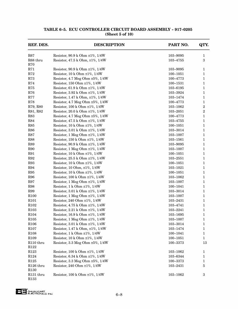
6-8
TABLE 6-5. ECU CONTROLLER CIRCUIT BOARD ASSEMBLY - 917-0205
(Sheet 5 of 10)
REF. DES. DESCRIPTION PART NO. QTY.
R67 Resistor, 90.9 k Ohm ±1%, 1/4W 103-9095 1
R68 thru Resistor, 47.5 k Ohm, ±1%, 1/4W 103-4755 3
R70
R71 Resistor, 90.9 k Ohm ±1%, 1/4W 103-9095 1
R72 Resistor, 10 k Ohm ±1%, 1/4W 100-1051 1
R73 Resistor, 4.7 Meg Ohm ±5%, 1/4W 100-4773 1
R74 Resistor, 150 Ohm ±1%, 1/4W 100-1531 1
R75 Resistor, 61.9 k Ohm ±1%, 1/4W 103-6195 1
R76 Resistor, 3.92 k Ohm ±1%, 1/4W 103-3924 1
R77 Resistor, 1.47 k Ohm, ±1%, 1/4W 103-1474 1
R78 Resistor, 4.7 Meg Ohm ±5%, 1/4W 100-4773 1
R79, R80 Resistor, 100 k Ohm ±1%, 1/4W 103-1062 2
R81, R82 Resistor, 20.0 k Ohm ±1%, 1/4W 103-2051 2
R83 Resistor, 4.7 Meg Ohm ±5%, 1/4W 100-4773 1
R84 Resistor, 47.5 k Ohm ±1%, 1/4W 103-4755 1
R85 Resistor, 10 k Ohm ±1%, 1/4W 100-1051 1
R86 Resistor, 3.01 k Ohm ±1%, 1/4W 103-3014 1
R87 Resistor, 1 Meg Ohm ±1%, 1/4W 103-1007 1
R88 Resistor, 150 k Ohm ±1%, 1/4W 103-1561 1
R89 Resistor, 90.9 k Ohm ±1%, 1/4W 103-9095 1
R90 Resistor, 1 Meg Ohm ±1%, 1/4W 103-1007 1
R91 Resistor, 10 k Ohm ±1%, 1/4W 100-1051 1
R92 Resistor, 25.5 k Ohm ±1%, 1/4W 103-2551 1
R93 Resistor, 10 k Ohm ±1%, 1/4W 100-1051 1
R94 Resistor, 10 Ohm, ±1%, 1/4W 103-1021 1
R95 Resistor, 10 k Ohm ±1%, 1/4W 100-1051 1
R96 Resistor, 100 k Ohm ±1%, 1/4W 103-1062 1
R97 Resistor, 1 Meg Ohm ±1%, 1/4W 103-1007 1
R98 Resistor, 1 k Ohm ±1%, 1/4W 100-1041 1
R99 Resistor, 3.01 k Ohm ±1%, 1/4W 103-3014 1
R100 Resistor, 1 Meg Ohm ±1%, 1/4W 103-1007 1
R101 Resistor, 240 Ohm ±1%, 1/4W 103-2431 1
R102 Resistor, 4.75 k Ohm ±1%, 1/4W 103-4741 1
R103 Resistor, 2.21 k Ohm ±1%, 1/4W 103-2241 1
R104 Resistor, 16.9 k Ohm ±1%, 1/4W 103-1695 1
R105 Resistor, 1 Meg Ohm ±1%, 1/4W 103-1007 1
R106 Resistor, 3.01 k Ohm ±1%, 1/4W 103-3014 1
R107 Resistor, 1.47 k Ohm, ±1%, 1/4W 103-1474 1
R108 Resistor, 1 k Ohm ±1%, 1/4W 100-1041 1
R109 Resistor, 10 k Ohm ±1%, 1/4W 100-1051 1
R110 thru Resistor, 3.3 Meg Ohm ±5%, 1/4W 100-3373 13
R122
R123 Resistor, 100 k Ohm ±1%, 1/4W 103-1062 1
R124 Resistor, 6.34 k Ohm ±1%, 1/4W 103-6344 1
R125 Resistor, 3.3 Meg Ohm ±5%, 1/4W 100-3373 1
R126 thru Resistor, 240 Ohm ±1%, 1/4W 103-2431 5
R130
R131 thru Resistor, 100 k Ohm ±1%, 1/4W 103-1062 3
R133

6-9
TABLE 6-5. ECU CONTROLLER CIRCUIT BOARD ASSEMBLY - 917-0205
(Sheet 6 of 10)
REF. DES. DESCRIPTION PART NO. QTY.
R134 Resistor, 10 k Ohm ±1%, 1/4W 100-1051 1
R135 Resistor, 1 k Ohm ±1%, 1/4W 100-1041 1
R136 Resistor, 90.9 k Ohm ±1%, 1/4W 103-9095 1
R137 Resistor, 10 k Ohm ±1%, 1/4W 100-1051 1
R138 Resistor, 100 k Ohm ±1%, 1/4W 103-1062 1
R139, R140 Resistor, 1 k Ohm ±1%, 1/4W 100-1041 2
R141 Resistor, 100 k Ohm ±1%, 1/4W 103-1062 1
R142 Resistor, 1 k Ohm ±1%, 1/4W 100-1041 1
R143 Potentiometer, 500 Ohm ±10%, 1 1/4W 178-5001 1
R144 Resistor, 750 Ohm ±1%, 1/4W 103-7503 1
R145 thru Resistor, 90.9 k Ohm ±1%, 1/4W 103-9095 3
R147
R148 thru Resistor, 47.5 k Ohm, ±1%, 1/4W 103-4755 3
R150
R151 Resistor, 90.9 k Ohm ±1%, 1/4W 103-9095 1
R152 Resistor, 10 k Ohm ±1%, 1/4W 100-1051 1
R153 Resistor, 499 Ohm ±1%, 1/4W 103-4993 1
R154, R155 Resistor, 10 k Ohm ±1%, 1/4W 100-1051 2
R156 Resistor, 1 k Ohm ±1%, 1/4W 100-1041 1
R157 Resistor, 90.9 k Ohm ±1%, 1/4W 103-9095 1
R158 Resistor, 10 k Ohm ±1%, 1/4W 100-1051 1
R159 Resistor, 100 k Ohm ±1%, 1/4W 103-1062 1
R160 Resistor, 1 k Ohm ±1%, 1/4W 100-1041 1
R161 Resistor, 301 k Ohm ±1%, 1/4W 103-3061 1
R162 Resistor, 100 k Ohm ±1%, 1/4W 103-1062 1
R163 Resistor, 499 Ohm ±1%, 1/4W 103-4993 1
R164, R165 Resistor, 10 k Ohm ±1%, 1/4W 100-1051 2
R166 Resistor, 100 k Ohm ±1%, 1/4W 103-1062 1
R167 Resistor, 3.3 Meg Ohm ±5%, 1/4W 100-3373 1
R168 Resistor, 10 k Ohm ±1%, 1/4W 100-1051 1
R169 Resistor, 100 k Ohm ±1%, 1/4W 103-1062 1
R170 Resistor, 1 k Ohm ±1%, 1/4W 100-1041 1
R171 Resistor, 26.1 k Ohm, ±1%, 1/4W 103-2615 1
R172, R173 Resistor, 100 k Ohm ±1%, 1/4W 103-1062 2
R174 thru Resistor, 10 k Ohm ±1%, 1/4W 100-1051 3
R176
R177 Resistor, 1 Meg Ohm ±1%, 1/4W 103-1007 1
R179, R181 Resistor, 1 k Ohm ±1%, 1/4W 100-1041 2
R183, R184 Resistor, 392 Ohm ±1%, 1/4W 103-3923 2
R187, R188 Resistor, 100 k Ohm ±1%, 1/4W 103-1062 2
R189 Resistor, 20.0 k Ohm ±1%, 1/4W 103-2051 1
R190 Resistor, 10 k Ohm ±1%, 1/4W 100-1051 1
R191 Resistor, 4.7 Meg Ohm ±5%, 1/4W 100-4773 1
R192 thru Resistor, 10 k Ohm ±1%, 1/4W 100-1051 1
R194
R195 Resistor, 26.1 k Oh ±1%, 1/4W 103-2615 1
R196 Resistor, 121 k Ohm ±1%, 1/4W 103-1261 1
R197 Resistor, 10 Ohm ±1%, 1/4W 103-1021 1

6-10
TABLE 6-5. ECU CONTROLLER CIRCUIT BOARD ASSEMBLY - 917-0205
(Sheet 7 of 10)
REF. DES. DESCRIPTION PART NO. QTY.
R198 Resistor, 100 k Ohm ±1%, 1/4W 103-1062 1
R199 Resistor, 4.75 k Ohm ±1%, 1/4W 103-4741 1
R200 Resistor, 2.2 Meg Ohm ±5%, 1/4W 100-2273 1
R201 thru Resistor, 100 k Ohm ±1%, 1/4W 103-1062 5
R205
R206 Resistor, 475 k Ohm ±1%, 1/4W 103-4731 1
R207, R208 Resistor, 100 k Ohm ±1%, 1/4W 103-1062 2
R209 Resistor, 1.47 k Ohm, ±1%, 1/4W 103-1474 1
R210 Resistor, 499 Ohm ±1%, 1/4W 103-4993 1
RN1, RN2 Resistor Network, 10 k Ohm ±2%, 1W Resistors, 8-Pin Single 226-1051 2
In-Line Package
RN3, RN4 Resistor Network, 9-100 k Ohm, ±2%, .17W Resistors, 10-Pin Single 226-1060 2
In-Line Package
RN5 Resistor Network, 10 k Ohm ±2%, 1W Resistors, 8-Pin Single 226-1051 1
In-Line Package
RN6, RN7 Resistor Network, 9-100 k Ohm, ±2%, 2.7W Resistors, 10-Pin Single 226-1060 2
In-Line Package
RN8 Resistor Network, 10 k Ohm ±2%, 1W Resistors, 8-Pin Single 226-1051 1
In-Line Package
S1 thru Switch, SPST, 4-Position, 8-Pin DIP Dual In-Line 340-0002 3
S3
S4 Switch, Miniature Toggle, DPDT, 0.4 vA Maximum at 20V ac or dc 340-0060 1
S5 Switch, Push, N.O. Momentary Contact, Miniature, 1A @ 120V 343-6330 1
Maximum
TP1 thru Test, Jack, Right Angle PC Mounting 417-0004 6
TP6
TP7 thru Terminal, Turret, Double Shoulder 413-1597 6
TP12
U1 thru Integrated Circuit, 4N33, Optical Isolator, NPN Photo 229-0033 11
U11 Transistor/Infared Emitting Diode Type, 1500V Isolation,
Response: 30 kHz Maximum, Current: 50 mA Maximum, 6-Pin DIP
U12 Integrated Circuit, CD4075BE, RCA 225-0006 1
U13 Integrated Circuit, CD4071B, OR Gate, CMOS, 14-Pin DIP 225-0005 1
U14 Integrated Circuit, MC14532B, 8-Bit Priority Encoder, CMOS, 228-4532 1
16-Pin DIP
U15 Integrated Circuit, MC14076, Quad D Register, CMOS, 16-Pin DIP 228-4076 1
U16 Integrated Circuit, MC14011BCP, Quad 2-Input NAND Gate, CMOS, 228-4011 1
14-Pin DIP
U17 Integrated Circuit, MC14076, Quad D Register, CMOS, 16-Pin DIP 228-4076 1
U18 Integrated Circuit, MC14028BCP, BCD-to-Decimal Decoder, CMOS 228-4028 1
U19 Integrated Circuit, CD4075BE, RCA 225-0006 1
U20 Integrated Circuit, CD4081B, Quad 2-Input AND Gate, CMOS, 225-0008 1
14-Pin DIP
U21 Integrated Circuit, CD4075BE, RCA 225-0006 1
U22 Integrated Circuit, MC14073B, Tripple 3-Input AND Gate, 228-4073 1
CMOS, 14-Pin DIP
U23 Integrated Circuit, MC14001, CMOS, Quad 2-Input NOR Gate, 228-4001 1
14-Pin DIP
U24 Integrated Circuit, Triple 3 Input NOR Gates, CMOS, 14-Pin DIP 220-4025 1
U25 Integrated Circuit, CD4069CN, Hex Inverter, CMOS, 14-Pin DIP 228-4069 1
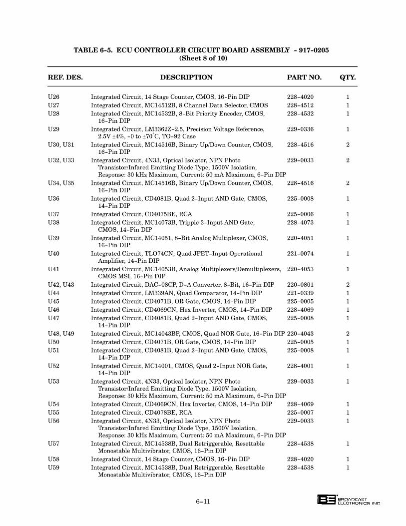
6-11
TABLE 6-5. ECU CONTROLLER CIRCUIT BOARD ASSEMBLY - 917-0205
(Sheet 8 of 10)
REF. DES. DESCRIPTION PART NO. QTY.
U26 Integrated Circuit, 14 Stage Counter, CMOS, 16-Pin DIP 228-4020 1
U27 Integrated Circuit, MC14512B, 8 Channel Data Selector, CMOS 228-4512 1
U28 Integrated Circuit, MC14532B, 8-Bit Priority Encoder, CMOS, 228-4532 1
16-Pin DIP
U29 Integrated Circuit, LM3362Z-2.5, Precision Voltage Reference, 229-0336 1
2.5V ±4%, -0 to ±70°C, TO-92 Case
U30, U31 Integrated Circuit, MC14516B, Binary Up/Down Counter, CMOS, 228-4516 2
16-Pin DIP
U32, U33 Integrated Circuit, 4N33, Optical Isolator, NPN Photo 229-0033 2
Transistor/Infared Emitting Diode Type, 1500V Isolation,
Response: 30 kHz Maximum, Current: 50 mA Maximum, 6-Pin DIP
U34, U35 Integrated Circuit, MC14516B, Binary Up/Down Counter, CMOS, 228-4516 2
16-Pin DIP
U36 Integrated Circuit, CD4081B, Quad 2-Input AND Gate, CMOS, 225-0008 1
14-Pin DIP
U37 Integrated Circuit, CD4075BE, RCA 225-0006 1
U38 Integrated Circuit, MC14073B, Tripple 3-Input AND Gate, 228-4073 1
CMOS, 14-Pin DIP
U39 Integrated Circuit, MC14051, 8-Bit Analog Multiplexer, CMOS, 220-4051 1
16-Pin DIP
U40 Integrated Circuit, TLO74CN, Quad JFET-Input Operational 221-0074 1
Amplifier, 14-Pin DIP
U41 Integrated Circuit, MC14053B, Analog Multiplexers/Demultiplexers, 220-4053 1
CMOS MSI, 16-Pin DIP
U42, U43 Integrated Circuit, DAC-08CP, D-A Converter, 8-Bit, 16-Pin DIP 220-0801 2
U44 Integrated Circuit, LM339AN, Quad Comparator, 14-Pin DIP 221-0339 1
U45 Integrated Circuit, CD4071B, OR Gate, CMOS, 14-Pin DIP 225-0005 1
U46 Integrated Circuit, CD4069CN, Hex Inverter, CMOS, 14-Pin DIP 228-4069 1
U47 Integrated Circuit, CD4081B, Quad 2-Input AND Gate, CMOS, 225-0008 1
14-Pin DIP
U48, U49 Integrated Circuit, MC14043BP, CMOS, Quad NOR Gate, 16-Pin DIP 220-4043 2
U50 Integrated Circuit, CD4071B, OR Gate, CMOS, 14-Pin DIP 225-0005 1
U51 Integrated Circuit, CD4081B, Quad 2-Input AND Gate, CMOS, 225-0008 1
14-Pin DIP
U52 Integrated Circuit, MC14001, CMOS, Quad 2-Input NOR Gate, 228-4001 1
14-Pin DIP
U53 Integrated Circuit, 4N33, Optical Isolator, NPN Photo 229-0033 1
Transistor/Infared Emitting Diode Type, 1500V Isolation,
Response: 30 kHz Maximum, Current: 50 mA Maximum, 6-Pin DIP
U54 Integrated Circuit, CD4069CN, Hex Inverter, CMOS, 14-Pin DIP 228-4069 1
U55 Integrated Circuit, CD4078BE, RCA 225-0007 1
U56 Integrated Circuit, 4N33, Optical Isolator, NPN Photo 229-0033 1
Transistor/Infared Emitting Diode Type, 1500V Isolation,
Response: 30 kHz Maximum, Current: 50 mA Maximum, 6-Pin DIP
U57 Integrated Circuit, MC14538B, Dual Retriggerable, Resettable 228-4538 1
Monostable Multivibrator, CMOS, 16-Pin DIP
U58 Integrated Circuit, 14 Stage Counter, CMOS, 16-Pin DIP 228-4020 1
U59 Integrated Circuit, MC14538B, Dual Retriggerable, Resettable 228-4538 1
Monostable Multivibrator, CMOS, 16-Pin DIP
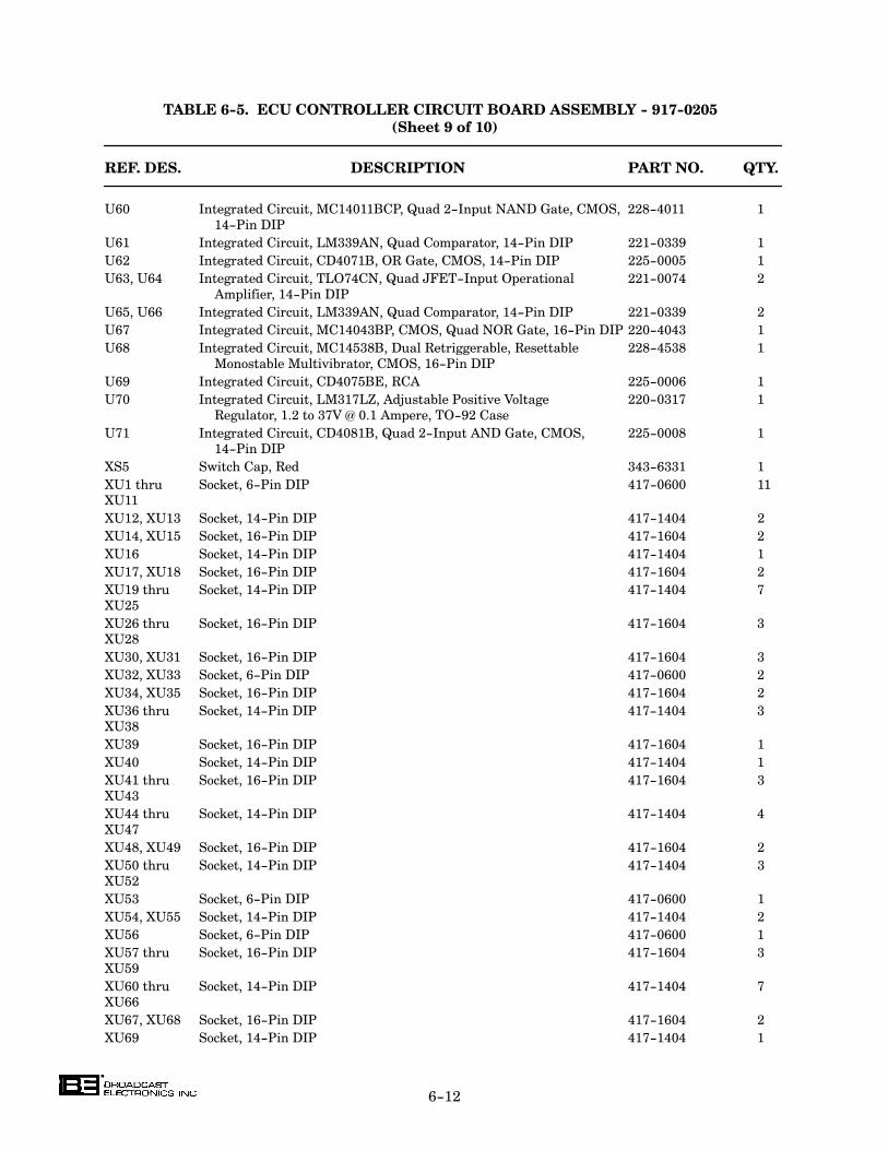
6-12
TABLE 6-5. ECU CONTROLLER CIRCUIT BOARD ASSEMBLY - 917-0205
(Sheet 9 of 10)
REF. DES. DESCRIPTION PART NO. QTY.
U60 Integrated Circuit, MC14011BCP, Quad 2-Input NAND Gate, CMOS, 228-4011 1
14-Pin DIP
U61 Integrated Circuit, LM339AN, Quad Comparator, 14-Pin DIP 221-0339 1
U62 Integrated Circuit, CD4071B, OR Gate, CMOS, 14-Pin DIP 225-0005 1
U63, U64 Integrated Circuit, TLO74CN, Quad JFET-Input Operational 221-0074 2
Amplifier, 14-Pin DIP
U65, U66 Integrated Circuit, LM339AN, Quad Comparator, 14-Pin DIP 221-0339 2
U67 Integrated Circuit, MC14043BP, CMOS, Quad NOR Gate, 16-Pin DIP 220-4043 1
U68 Integrated Circuit, MC14538B, Dual Retriggerable, Resettable 228-4538 1
Monostable Multivibrator, CMOS, 16-Pin DIP
U69 Integrated Circuit, CD4075BE, RCA 225-0006 1
U70 Integrated Circuit, LM317LZ, Adjustable Positive Voltage 220-0317 1
Regulator, 1.2 to 37V @ 0.1 Ampere, TO-92 Case
U71 Integrated Circuit, CD4081B, Quad 2-Input AND Gate, CMOS, 225-0008 1
14-Pin DIP
XS5 Switch Cap, Red 343-6331 1
XU1 thru Socket, 6-Pin DIP 417-0600 11
XU11
XU12, XU13 Socket, 14-Pin DIP 417-1404 2
XU14, XU15 Socket, 16-Pin DIP 417-1604 2
XU16 Socket, 14-Pin DIP 417-1404 1
XU17, XU18 Socket, 16-Pin DIP 417-1604 2
XU19 thru Socket, 14-Pin DIP 417-1404 7
XU25
XU26 thru Socket, 16-Pin DIP 417-1604 3
XU28
XU30, XU31 Socket, 16-Pin DIP 417-1604 3
XU32, XU33 Socket, 6-Pin DIP 417-0600 2
XU34, XU35 Socket, 16-Pin DIP 417-1604 2
XU36 thru Socket, 14-Pin DIP 417-1404 3
XU38
XU39 Socket, 16-Pin DIP 417-1604 1
XU40 Socket, 14-Pin DIP 417-1404 1
XU41 thru Socket, 16-Pin DIP 417-1604 3
XU43
XU44 thru Socket, 14-Pin DIP 417-1404 4
XU47
XU48, XU49 Socket, 16-Pin DIP 417-1604 2
XU50 thru Socket, 14-Pin DIP 417-1404 3
XU52
XU53 Socket, 6-Pin DIP 417-0600 1
XU54, XU55 Socket, 14-Pin DIP 417-1404 2
XU56 Socket, 6-Pin DIP 417-0600 1
XU57 thru Socket, 16-Pin DIP 417-1604 3
XU59
XU60 thru Socket, 14-Pin DIP 417-1404 7
XU66
XU67, XU68 Socket, 16-Pin DIP 417-1604 2
XU69 Socket, 14-Pin DIP 417-1404 1
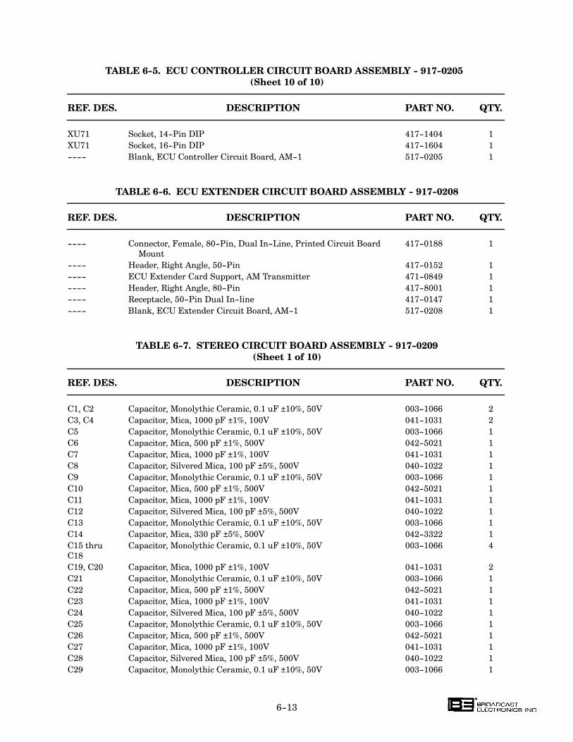
6-13
TABLE 6-5. ECU CONTROLLER CIRCUIT BOARD ASSEMBLY - 917-0205
(Sheet 10 of 10)
REF. DES. DESCRIPTION PART NO. QTY.
XU71 Socket, 14-Pin DIP 417-1404 1
XU71 Socket, 16-Pin DIP 417-1604 1
---- Blank, ECU Controller Circuit Board, AM-1 517-0205 1
TABLE 6-6. ECU EXTENDER CIRCUIT BOARD ASSEMBLY - 917-0208
REF. DES. DESCRIPTION PART NO. QTY.
---- Connector, Female, 80-Pin, Dual In-Line, Printed Circuit Board 417-0188 1
Mount
---- Header, Right Angle, 50-Pin 417-0152 1
---- ECU Extender Card Support, AM Transmitter 471-0849 1
---- Header, Right Angle, 80-Pin 417-8001 1
---- Receptacle, 50-Pin Dual In-line 417-0147 1
---- Blank, ECU Extender Circuit Board, AM-1 517-0208 1
TABLE 6-7. STEREO CIRCUIT BOARD ASSEMBLY - 917-0209
(Sheet 1 of 10)
REF. DES. DESCRIPTION PART NO. QTY.
C1, C2 Capacitor, Monolythic Ceramic, 0.1 uF ±10%, 50V 003-1066 2
C3, C4 Capacitor, Mica, 1000 pF ±1%, 100V 041-1031 2
C5 Capacitor, Monolythic Ceramic, 0.1 uF ±10%, 50V 003-1066 1
C6 Capacitor, Mica, 500 pF ±1%, 500V 042-5021 1
C7 Capacitor, Mica, 1000 pF ±1%, 100V 041-1031 1
C8 Capacitor, Silvered Mica, 100 pF ±5%, 500V 040-1022 1
C9 Capacitor, Monolythic Ceramic, 0.1 uF ±10%, 50V 003-1066 1
C10 Capacitor, Mica, 500 pF ±1%, 500V 042-5021 1
C11 Capacitor, Mica, 1000 pF ±1%, 100V 041-1031 1
C12 Capacitor, Silvered Mica, 100 pF ±5%, 500V 040-1022 1
C13 Capacitor, Monolythic Ceramic, 0.1 uF ±10%, 50V 003-1066 1
C14 Capacitor, Mica, 330 pF ±5%, 500V 042-3322 1
C15 thru Capacitor, Monolythic Ceramic, 0.1 uF ±10%, 50V 003-1066 4
C18
C19, C20 Capacitor, Mica, 1000 pF ±1%, 100V 041-1031 2
C21 Capacitor, Monolythic Ceramic, 0.1 uF ±10%, 50V 003-1066 1
C22 Capacitor, Mica, 500 pF ±1%, 500V 042-5021 1
C23 Capacitor, Mica, 1000 pF ±1%, 100V 041-1031 1
C24 Capacitor, Silvered Mica, 100 pF ±5%, 500V 040-1022 1
C25 Capacitor, Monolythic Ceramic, 0.1 uF ±10%, 50V 003-1066 1
C26 Capacitor, Mica, 500 pF ±1%, 500V 042-5021 1
C27 Capacitor, Mica, 1000 pF ±1%, 100V 041-1031 1
C28 Capacitor, Silvered Mica, 100 pF ±5%, 500V 040-1022 1
C29 Capacitor, Monolythic Ceramic, 0.1 uF ±10%, 50V 003-1066 1
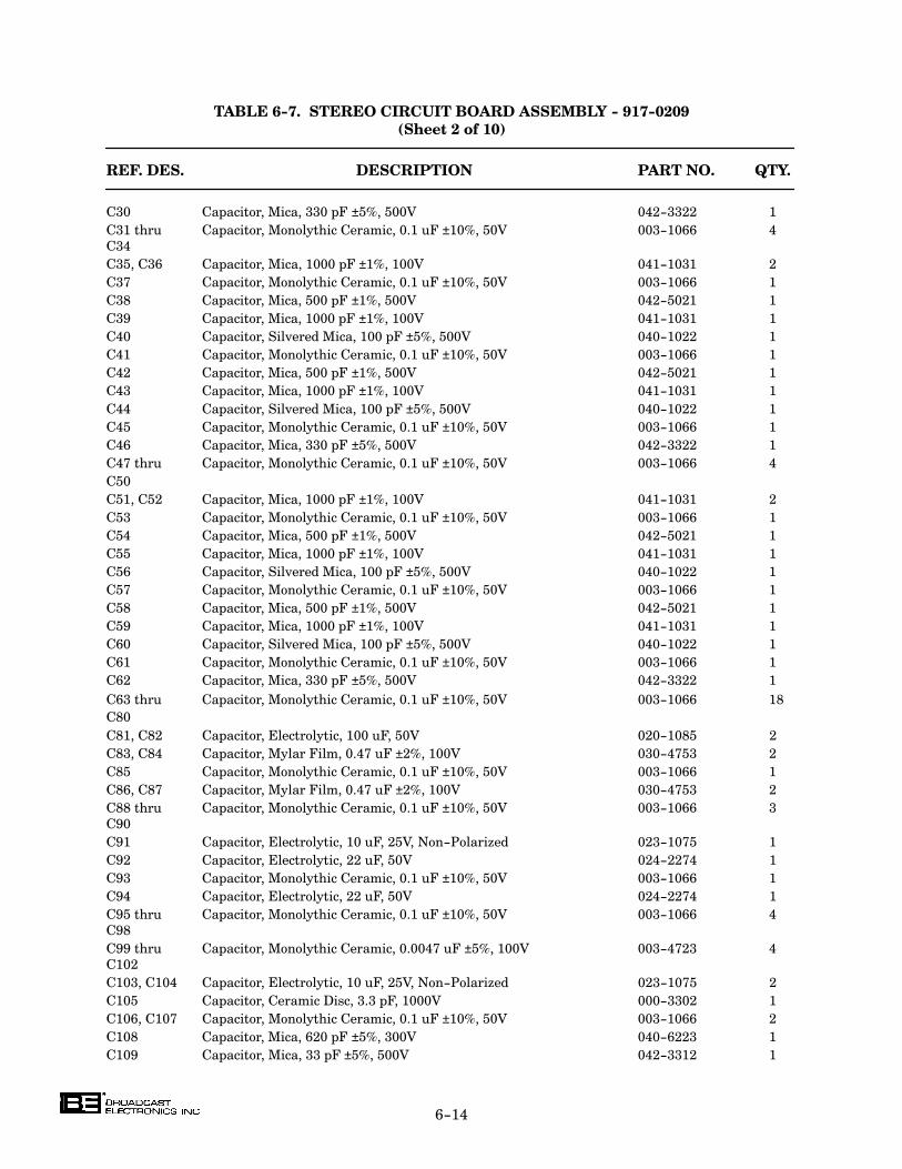
6-14
TABLE 6-7. STEREO CIRCUIT BOARD ASSEMBLY - 917-0209
(Sheet 2 of 10)
REF. DES. DESCRIPTION PART NO. QTY.
C30 Capacitor, Mica, 330 pF ±5%, 500V 042-3322 1
C31 thru Capacitor, Monolythic Ceramic, 0.1 uF ±10%, 50V 003-1066 4
C34
C35, C36 Capacitor, Mica, 1000 pF ±1%, 100V 041-1031 2
C37 Capacitor, Monolythic Ceramic, 0.1 uF ±10%, 50V 003-1066 1
C38 Capacitor, Mica, 500 pF ±1%, 500V 042-5021 1
C39 Capacitor, Mica, 1000 pF ±1%, 100V 041-1031 1
C40 Capacitor, Silvered Mica, 100 pF ±5%, 500V 040-1022 1
C41 Capacitor, Monolythic Ceramic, 0.1 uF ±10%, 50V 003-1066 1
C42 Capacitor, Mica, 500 pF ±1%, 500V 042-5021 1
C43 Capacitor, Mica, 1000 pF ±1%, 100V 041-1031 1
C44 Capacitor, Silvered Mica, 100 pF ±5%, 500V 040-1022 1
C45 Capacitor, Monolythic Ceramic, 0.1 uF ±10%, 50V 003-1066 1
C46 Capacitor, Mica, 330 pF ±5%, 500V 042-3322 1
C47 thru Capacitor, Monolythic Ceramic, 0.1 uF ±10%, 50V 003-1066 4
C50
C51, C52 Capacitor, Mica, 1000 pF ±1%, 100V 041-1031 2
C53 Capacitor, Monolythic Ceramic, 0.1 uF ±10%, 50V 003-1066 1
C54 Capacitor, Mica, 500 pF ±1%, 500V 042-5021 1
C55 Capacitor, Mica, 1000 pF ±1%, 100V 041-1031 1
C56 Capacitor, Silvered Mica, 100 pF ±5%, 500V 040-1022 1
C57 Capacitor, Monolythic Ceramic, 0.1 uF ±10%, 50V 003-1066 1
C58 Capacitor, Mica, 500 pF ±1%, 500V 042-5021 1
C59 Capacitor, Mica, 1000 pF ±1%, 100V 041-1031 1
C60 Capacitor, Silvered Mica, 100 pF ±5%, 500V 040-1022 1
C61 Capacitor, Monolythic Ceramic, 0.1 uF ±10%, 50V 003-1066 1
C62 Capacitor, Mica, 330 pF ±5%, 500V 042-3322 1
C63 thru Capacitor, Monolythic Ceramic, 0.1 uF ±10%, 50V 003-1066 18
C80
C81, C82 Capacitor, Electrolytic, 100 uF, 50V 020-1085 2
C83, C84 Capacitor, Mylar Film, 0.47 uF ±2%, 100V 030-4753 2
C85 Capacitor, Monolythic Ceramic, 0.1 uF ±10%, 50V 003-1066 1
C86, C87 Capacitor, Mylar Film, 0.47 uF ±2%, 100V 030-4753 2
C88 thru Capacitor, Monolythic Ceramic, 0.1 uF ±10%, 50V 003-1066 3
C90
C91 Capacitor, Electrolytic, 10 uF, 25V, Non-Polarized 023-1075 1
C92 Capacitor, Electrolytic, 22 uF, 50V 024-2274 1
C93 Capacitor, Monolythic Ceramic, 0.1 uF ±10%, 50V 003-1066 1
C94 Capacitor, Electrolytic, 22 uF, 50V 024-2274 1
C95 thru Capacitor, Monolythic Ceramic, 0.1 uF ±10%, 50V 003-1066 4
C98
C99 thru Capacitor, Monolythic Ceramic, 0.0047 uF ±5%, 100V 003-4723 4
C102
C103, C104 Capacitor, Electrolytic, 10 uF, 25V, Non-Polarized 023-1075 2
C105 Capacitor, Ceramic Disc, 3.3 pF, 1000V 000-3302 1
C106, C107 Capacitor, Monolythic Ceramic, 0.1 uF ±10%, 50V 003-1066 2
C108 Capacitor, Mica, 620 pF ±5%, 300V 040-6223 1
C109 Capacitor, Mica, 33 pF ±5%, 500V 042-3312 1
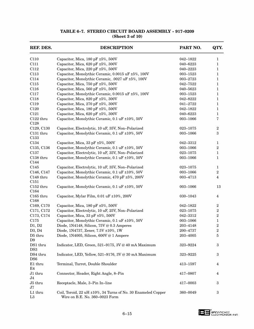
6-15
TABLE 6-7. STEREO CIRCUIT BOARD ASSEMBLY - 917-0209
(Sheet 3 of 10)
REF. DES. DESCRIPTION PART NO. QTY.
C110 Capacitor, Mica, 180 pF ±5%, 500V 042-1822 1
C111 Capacitor, Mica, 620 pF ±5%, 300V 040-6223 1
C112 Capacitor, Mica, 220 pF ±5%, 500V 040-2223 1
C113 Capacitor, Monolythic Ceramic, 0.0015 uF ±5%, 100V 003-1523 1
C114 Capacitor, Monolythic Ceramic, .0027 uF ±5%, 100V 003-2723 1
C115 Capacitor, Mica, 750 pF ±5%, 500V 042-7522 1
C116 Capacitor, Mica, 560 pF ±5%, 500V 040-5623 1
C117 Capacitor, Monolythic Ceramic, 0.0015 uF ±5%, 100V 003-1523 1
C118 Capacitor, Mica, 820 pF ±5%, 300V 042-8222 1
C119 Capacitor, Mica, 270 pF ±5%, 300V 041-2722 1
C120 Capacitor, Mica, 180 pF ±5%, 500V 042-1822 1
C121 Capacitor, Mica, 620 pF ±5%, 300V 040-6223 1
C122 thru Capacitor, Monolythic Ceramic, 0.1 uF ±10%, 50V 003-1066 7
C128
C129, C130 Capacitor, Electrolytic, 10 uF, 35V, Non-Polarized 023-1075 2
C131 thru Capacitor, Monolythic Ceramic, 0.1 uF ±10%, 50V 003-1066 3
C133
C134 Capacitor, Mica, 33 pF ±5%, 500V 042-3312 1
C135, C136 Capacitor, Monolythic Ceramic, 0.1 uF ±10%, 50V 003-1066 2
C137 Capacitor, Electrolytic, 10 uF, 35V, Non-Polarized 023-1075 1
C138 thru Capacitor, Monolythic Ceramic, 0.1 uF ±10%, 50V 003-1066 1
C144
C145 Capacitor, Electrolytic, 10 uF, 35V, Non-Polarized 023-1075 1
C146, C147 Capacitor, Monolythic Ceramic, 0.1 uF ±10%, 50V 003-1066 2
C148 thru Capacitor, Monolythic Ceramic, 470 pF ±5%, 200V 003-4713 4
C151
C152 thru Capacitor, Monolythic Ceramic, 0.1 uF ±10%, 50V 003-1066 13
C164
C165 thru Capacitor, Mylar Film, 0.01 uF ±10%, 200V 030-1043 4
C168
C169, C170 Capacitor, Mica, 180 pF ±5%, 500V 042-1822 2
C171, C172 Capacitor, Electrolytic, 10 uF, 25V, Non-Polarized 023-1075 2
C173, C174 Capacitor, Mica, 33 pF ±5%, 500V 042-3312 2
C175 Capacitor, Monolythic Ceramic, 0.1 uF ±10%, 50V 003-1066 1
D1, D2 Diode, 1N4148, Silicon, 75V @ 0.3 Amperes 203-4148 2
D3, D4 Diode, 1N4737, Zener, 7.5V ±10%, 1W 200-4737 2
D5 thru Diode, 1N4005, Silicon, 600V @ 1 Ampere 203-4005 5
D9
DS1 thru Indicator, LED, Green, 521-9175, 3V @ 40 mA Maximum 323-9224 3
DS3
DS4 thru Indicator, LED, Yellow, 521-9176, 3V @ 30 mA Maximum 323-9225 3
DS6
E1 thru Terminal, Turret, Double Shoulder 413-1597 4
E4
J1 thru Connector, Header, Right Angle, 8-Pin 417-0807 4
J4
J5 thru Receptacle, Male, 3-Pin In-line 417-0003 3
J7
L1 thru Coil, Toroid, 22 uH ±10%, 34 Turns of No. 30 Enameled Copper 360-0049 3
L3 Wire on B.E. No. 360-0023 Form

6-16
TABLE 6-7. STEREO CIRCUIT BOARD ASSEMBLY - 917-0209
(Sheet 4 of 10)
REF. DES. DESCRIPTION PART NO. QTY.
L4 Shielded Adjustable Coil, 64-163 uH, 155 mA Maximum, 360-0077 1
9.98 Ohms DC Resistance
L5, L6 Shielded Adjustable Coil, 26-71 uH, 185 mA Maximum, 360-0062 2
6.97 Ohms DC Resistance
L7 Shielded Adjustable Coil, 12-29 uH, 225 mA Maximum, 360-0078 1
4.72 Ohms DC Resistance
P1, P2 Jumper, Programmable, 2-Pin 340-0004 2
P3 thru Jumper, Programmable, 2-Pin 340-0004 5
P7
P1A Jumper, Programmable, 2-Pin 340-0004 1
P2B Jumper, Programmable, 2-Pin 340-0004 1
P31 Jumper, Programmable, 2-Pin 340-0004 1
P201 Receptacle, 50-Pin Dual In-line 417-0147 1
Q1, Q2 Transistor, 2N3904, NPN, Silicon, TO-92 Case 211-3904 2
Q3 thru Transistor, 2N7000, FET, N-Channel, TO-92 Case 210-7000 12
Q14
R1 Potentiometer, 5 k Ohm ±10%, 1W 179-5043 1
R2 Resistor, 8.25 k Ohm ±1%, 1/4W 103-8254 1
R3 Resistor, 10 k Ohm ±1%, 1/4W 100-1051 1
R4 Resistor, 6.04 k Ohm, ±1%, 1/4W 103-6044 1
R5 Resistor, 10 k Ohm ±1%, 1/4W 100-1051 1
R6 Potentiometer, 10 k Ohm ±10%, 1 1/4W 179-1053 1
R7 Resistor, 24.9 k Ohm ±1%, 1/4W 103-2495 1
R8 Resistor, 51.1 Ohm ±1%, 1/4W 103-5112 1
R9 Resistor, 100 k Ohm ±1%, 1/4W 103-1062 1
R10 Potentiometer, 500 Ohm ±10%, 1 1/4W 178-5001 1
R11 Resistor, 10 k Ohm ±1%, 1/4W 100-1051 1
R12 Resistor, 4.75 k Ohm ±1%, 1/4W 103-4741 1
R13 Resistor, 24.9 k Ohm ±1%, 1/4W 103-2495 1
R14 Resistor, 51.1 Ohm ±1%, 1/4W 103-5112 1
R15 Resistor, 10 k Ohm ±1%, 1/4W 100-1051 1
R16 Resistor, 4.75 k Ohm ±1%, 1/4W 103-4741 1
R17 thru Resistor, 10 k Ohm ±1%, 1/4W 100-1051 3
R19
R20 thru Resistor, 4.99 k Ohm ±1%, 1/4W 100-5041 3
R22
R23, R24 Resistor, 10 k Ohm ±1%, 1/4W 100-1051 2
R25 Resistor, 1 k Ohm ±1%, 1/4W 100-1041 1
R26 Potentiometer, 10 k Ohm ±10%, 1 1/4W 179-1053 1
R27 Potentiometer, 5 k Ohm ±10%, 1W 179-5043 1
R28 Resistor, 8.25 k Ohm ±1%, 1/4W 103-8254 1
R29 Resistor, 10 k Ohm ±1%, 1/4W 100-1051 1
R30 Resistor, 6.04K Ohm, ±1%, 1/4W 103-6044 1
R31 Resistor, 10 k Ohm ±1%, 1/4W 100-1051 1
R32 Potentiometer, 10 k Ohm ±10%, 1 1/4W 179-1053 1
R33 Resistor, 24.9 k Ohm ±1%, 1/4W 103-2495 1
R34 Resistor, 51.1 Ohm ±1%, 1/4W 103-5112 1
R35 Resistor, 100 k Ohm ±1%, 1/4W 103-1062 1
R36 Potentiometer, 500 Ohm ±10%, 1 1/4W 178-5001 1

6-17
TABLE 6-7. STEREO CIRCUIT BOARD ASSEMBLY - 917-0209
(Sheet 5 of 10)
REF. DES. DESCRIPTION PART NO. QTY.
R37 Resistor, 10 k Ohm ±1%, 1/4W 100-1051 1
R38 Resistor, 4.75 k Ohm ±1%, 1/4W 103-4741 1
R39 Resistor, 24.9 k Ohm ±1%, 1/4W 103-2495 1
R40 Resistor, 51.1 Ohm ±1%, 1/4W 103-5112 1
R41 Resistor, 10 k Ohm ±1%, 1/4W 100-1051 1
R42 Resistor, 4.75 k Ohm ±1%, 1/4W 103-4741 1
R43 thru Resistor, 10 k Ohm ±1%, 1/4W 100-1051 3
R45
R46 thru Resistor, 4.99 k Ohm ±1%, 1/4W 100-5041 3
R48
R49, R50 Resistor, 10 k Ohm ±1%, 1/4W 100-1051 2
R51 Resistor, 1 k Ohm ±1%, 1/4W 100-1041 1
R52 Potentiometer, 10 k Ohm ±10%, 1 1/4W 179-1053 1
R53 Potentiometer, 5 k Ohm ±10%, 1W 179-5043 1
R54 Resistor, 8.25 k Ohm ±1%, 1/4W 103-8254 1
R55 Resistor, 10 k Ohm ±1%, 1/4W 100-1051 1
R56 Resistor, 6.04K Ohm ±1%, 1/4W 103-6044 1
R57 Resistor, 10 k Ohm ±1%, 1/4W 100-1051 1
R58 Potentiometer, 10 k Ohm ±10%, 1 1/4W 179-1053 1
R59 Resistor, 51.1 Ohm ±1%, 1/4W 103-5112 1
R60 Resistor, 24.9 k Ohm ±1%, 1/4W 103-2495 1
R61 Resistor, 100 k Ohm ±1%, 1/4W 103-1062 1
R62 Potentiometer, 500 Ohm ±10%, 1 1/4W 178-5001 1
R63 Resistor, 10 k Ohm ±1%, 1/4W 100-1051 1
R64 Resistor, 4.75 k Ohm ±1%, 1/4W 103-4741 1
R65 Resistor, 24.9 k Ohm ±1%, 1/4W 103-2495 1
R67 Resistor, 10 k Ohm ±1%, 1/4W 100-1051 1
R68 Resistor, 4.75 k Ohm ±1%, 1/4W 103-4741 1
R69 thru Resistor, 10 k Ohm ±1%, 1/4W 100-1051 3
R71
R72 thru Resistor, 4.99 k Ohm ±1%, 1/4W 100-5041 3
R74
R75, R76 Resistor, 10 k Ohm ±1%, 1/4W 100-1051 2
R77 Resistor, 1 k Ohm ±1%, 1/4W 100-1041 1
R78 Potentiometer, 10 k Ohm ±10%, 1 1/4W 179-1053 1
R79 Potentiometer, 5 k Ohm ±10%, 1W 179-5043 1
R80 Resistor, 8.25 k Ohm ±1%, 1/4W 103-8254 1
R81 Resistor, 10 k Ohm ±1%, 1/4W 100-1051 1
R82 Resistor, 6.04 k Ohm ±1%, 1/4W 103-6044 1
R83 Resistor, 10 k Ohm ±1%, 1/4W 100-1051 1
R84 Potentiometer, 10 k Ohm ±10%, 1 1/4W 179-1053 1
R85 Resistor, 24.9 k Ohm ±1%, 1/4W 103-2495 1
R86 Resistor, 51.1 Ohm ±1%, 1/4W 103-5112 1
R87 Resistor, 100 k Ohm ±1%, 1/4W 103-1062 1
R88 Potentiometer, 500 Ohm ±10%, 1 1/4W 178-5001 1
R89 Resistor, 10 k Ohm ±1%, 1/4W 100-1051 1
R90 Resistor, 4.75 k Ohm ±1%, 1/4W 103-4741 1
R91 Resistor, 24.9 k Ohm ±1%, 1/4W 103-2495 1
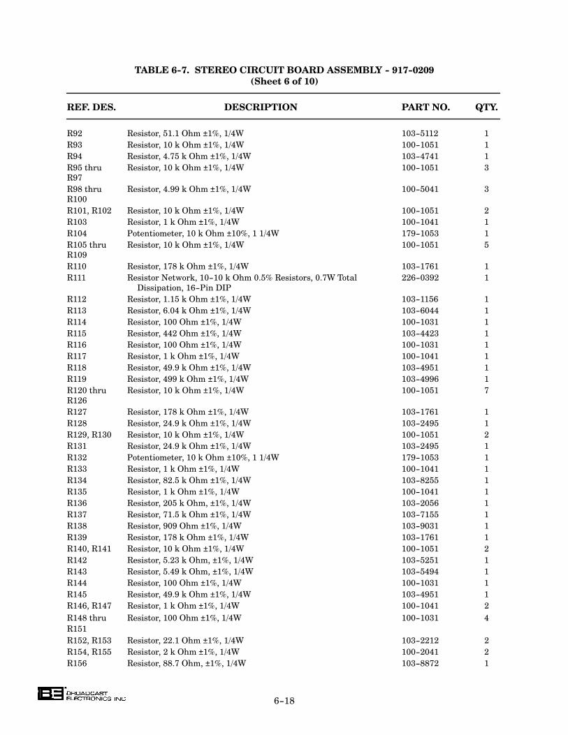
6-18
TABLE 6-7. STEREO CIRCUIT BOARD ASSEMBLY - 917-0209
(Sheet 6 of 10)
REF. DES. DESCRIPTION PART NO. QTY.
R92 Resistor, 51.1 Ohm ±1%, 1/4W 103-5112 1
R93 Resistor, 10 k Ohm ±1%, 1/4W 100-1051 1
R94 Resistor, 4.75 k Ohm ±1%, 1/4W 103-4741 1
R95 thru Resistor, 10 k Ohm ±1%, 1/4W 100-1051 3
R97
R98 thru Resistor, 4.99 k Ohm ±1%, 1/4W 100-5041 3
R100
R101, R102 Resistor, 10 k Ohm ±1%, 1/4W 100-1051 2
R103 Resistor, 1 k Ohm ±1%, 1/4W 100-1041 1
R104 Potentiometer, 10 k Ohm ±10%, 1 1/4W 179-1053 1
R105 thru Resistor, 10 k Ohm ±1%, 1/4W 100-1051 5
R109
R110 Resistor, 178 k Ohm ±1%, 1/4W 103-1761 1
R111 Resistor Network, 10-10 k Ohm 0.5% Resistors, 0.7W Total 226-0392 1
Dissipation, 16-Pin DIP
R112 Resistor, 1.15 k Ohm ±1%, 1/4W 103-1156 1
R113 Resistor, 6.04 k Ohm ±1%, 1/4W 103-6044 1
R114 Resistor, 100 Ohm ±1%, 1/4W 100-1031 1
R115 Resistor, 442 Ohm ±1%, 1/4W 103-4423 1
R116 Resistor, 100 Ohm ±1%, 1/4W 100-1031 1
R117 Resistor, 1 k Ohm ±1%, 1/4W 100-1041 1
R118 Resistor, 49.9 k Ohm ±1%, 1/4W 103-4951 1
R119 Resistor, 499 k Ohm ±1%, 1/4W 103-4996 1
R120 thru Resistor, 10 k Ohm ±1%, 1/4W 100-1051 7
R126
R127 Resistor, 178 k Ohm ±1%, 1/4W 103-1761 1
R128 Resistor, 24.9 k Ohm ±1%, 1/4W 103-2495 1
R129, R130 Resistor, 10 k Ohm ±1%, 1/4W 100-1051 2
R131 Resistor, 24.9 k Ohm ±1%, 1/4W 103-2495 1
R132 Potentiometer, 10 k Ohm ±10%, 1 1/4W 179-1053 1
R133 Resistor, 1 k Ohm ±1%, 1/4W 100-1041 1
R134 Resistor, 82.5 k Ohm ±1%, 1/4W 103-8255 1
R135 Resistor, 1 k Ohm ±1%, 1/4W 100-1041 1
R136 Resistor, 205 k Ohm, ±1%, 1/4W 103-2056 1
R137 Resistor, 71.5 k Ohm ±1%, 1/4W 103-7155 1
R138 Resistor, 909 Ohm ±1%, 1/4W 103-9031 1
R139 Resistor, 178 k Ohm ±1%, 1/4W 103-1761 1
R140, R141 Resistor, 10 k Ohm ±1%, 1/4W 100-1051 2
R142 Resistor, 5.23 k Ohm, ±1%, 1/4W 103-5251 1
R143 Resistor, 5.49 k Ohm, ±1%, 1/4W 103-5494 1
R144 Resistor, 100 Ohm ±1%, 1/4W 100-1031 1
R145 Resistor, 49.9 k Ohm ±1%, 1/4W 103-4951 1
R146, R147 Resistor, 1 k Ohm ±1%, 1/4W 100-1041 2
R148 thru Resistor, 100 Ohm ±1%, 1/4W 100-1031 4
R151
R152, R153 Resistor, 22.1 Ohm ±1%, 1/4W 103-2212 2
R154, R155 Resistor, 2 k Ohm ±1%, 1/4W 100-2041 2
R156 Resistor, 88.7 Ohm, ±1%, 1/4W 103-8872 1
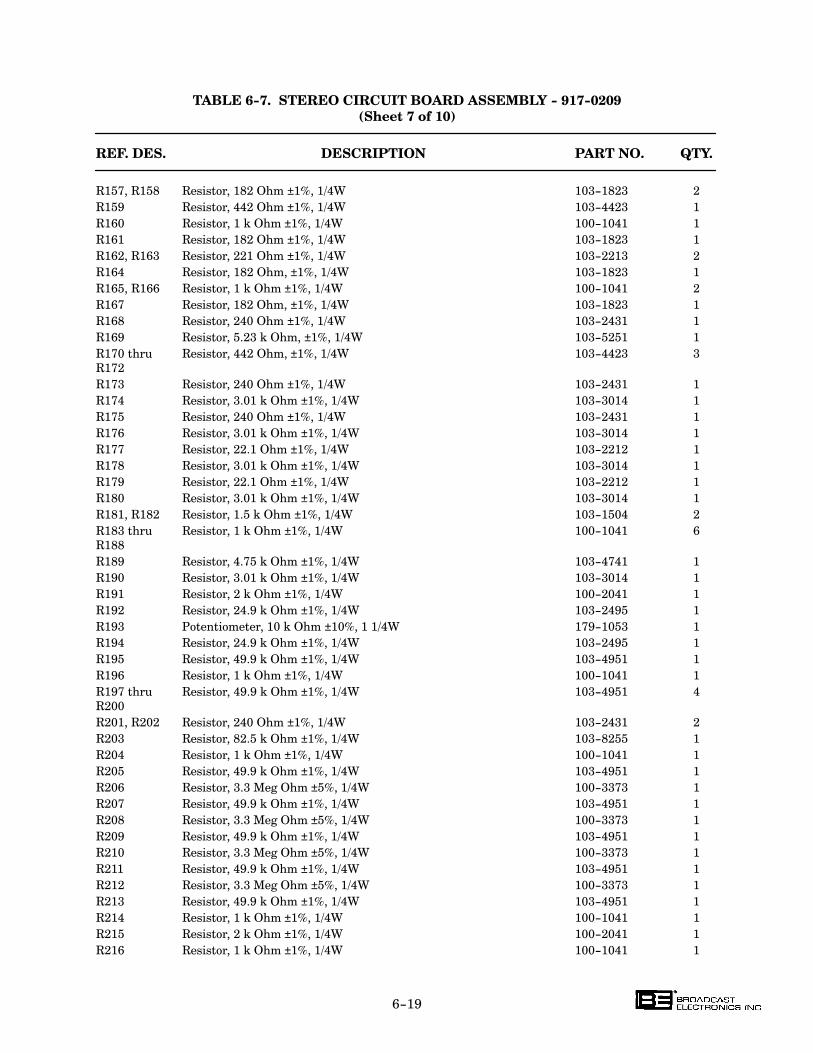
6-19
TABLE 6-7. STEREO CIRCUIT BOARD ASSEMBLY - 917-0209
(Sheet 7 of 10)
REF. DES. DESCRIPTION PART NO. QTY.
R157, R158 Resistor, 182 Ohm ±1%, 1/4W 103-1823 2
R159 Resistor, 442 Ohm ±1%, 1/4W 103-4423 1
R160 Resistor, 1 k Ohm ±1%, 1/4W 100-1041 1
R161 Resistor, 182 Ohm ±1%, 1/4W 103-1823 1
R162, R163 Resistor, 221 Ohm ±1%, 1/4W 103-2213 2
R164 Resistor, 182 Ohm, ±1%, 1/4W 103-1823 1
R165, R166 Resistor, 1 k Ohm ±1%, 1/4W 100-1041 2
R167 Resistor, 182 Ohm, ±1%, 1/4W 103-1823 1
R168 Resistor, 240 Ohm ±1%, 1/4W 103-2431 1
R169 Resistor, 5.23 k Ohm, ±1%, 1/4W 103-5251 1
R170 thru Resistor, 442 Ohm, ±1%, 1/4W 103-4423 3
R172
R173 Resistor, 240 Ohm ±1%, 1/4W 103-2431 1
R174 Resistor, 3.01 k Ohm ±1%, 1/4W 103-3014 1
R175 Resistor, 240 Ohm ±1%, 1/4W 103-2431 1
R176 Resistor, 3.01 k Ohm ±1%, 1/4W 103-3014 1
R177 Resistor, 22.1 Ohm ±1%, 1/4W 103-2212 1
R178 Resistor, 3.01 k Ohm ±1%, 1/4W 103-3014 1
R179 Resistor, 22.1 Ohm ±1%, 1/4W 103-2212 1
R180 Resistor, 3.01 k Ohm ±1%, 1/4W 103-3014 1
R181, R182 Resistor, 1.5 k Ohm ±1%, 1/4W 103-1504 2
R183 thru Resistor, 1 k Ohm ±1%, 1/4W 100-1041 6
R188
R189 Resistor, 4.75 k Ohm ±1%, 1/4W 103-4741 1
R190 Resistor, 3.01 k Ohm ±1%, 1/4W 103-3014 1
R191 Resistor, 2 k Ohm ±1%, 1/4W 100-2041 1
R192 Resistor, 24.9 k Ohm ±1%, 1/4W 103-2495 1
R193 Potentiometer, 10 k Ohm ±10%, 1 1/4W 179-1053 1
R194 Resistor, 24.9 k Ohm ±1%, 1/4W 103-2495 1
R195 Resistor, 49.9 k Ohm ±1%, 1/4W 103-4951 1
R196 Resistor, 1 k Ohm ±1%, 1/4W 100-1041 1
R197 thru Resistor, 49.9 k Ohm ±1%, 1/4W 103-4951 4
R200
R201, R202 Resistor, 240 Ohm ±1%, 1/4W 103-2431 2
R203 Resistor, 82.5 k Ohm ±1%, 1/4W 103-8255 1
R204 Resistor, 1 k Ohm ±1%, 1/4W 100-1041 1
R205 Resistor, 49.9 k Ohm ±1%, 1/4W 103-4951 1
R206 Resistor, 3.3 Meg Ohm ±5%, 1/4W 100-3373 1
R207 Resistor, 49.9 k Ohm ±1%, 1/4W 103-4951 1
R208 Resistor, 3.3 Meg Ohm ±5%, 1/4W 100-3373 1
R209 Resistor, 49.9 k Ohm ±1%, 1/4W 103-4951 1
R210 Resistor, 3.3 Meg Ohm ±5%, 1/4W 100-3373 1
R211 Resistor, 49.9 k Ohm ±1%, 1/4W 103-4951 1
R212 Resistor, 3.3 Meg Ohm ±5%, 1/4W 100-3373 1
R213 Resistor, 49.9 k Ohm ±1%, 1/4W 103-4951 1
R214 Resistor, 1 k Ohm ±1%, 1/4W 100-1041 1
R215 Resistor, 2 k Ohm ±1%, 1/4W 100-2041 1
R216 Resistor, 1 k Ohm ±1%, 1/4W 100-1041 1
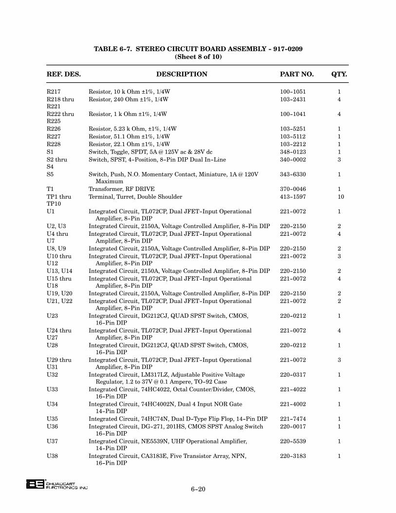
6-20
TABLE 6-7. STEREO CIRCUIT BOARD ASSEMBLY - 917-0209
(Sheet 8 of 10)
REF. DES. DESCRIPTION PART NO. QTY.
R217 Resistor, 10 k Ohm ±1%, 1/4W 100-1051 1
R218 thru Resistor, 240 Ohm ±1%, 1/4W 103-2431 4
R221
R222 thru Resistor, 1 k Ohm ±1%, 1/4W 100-1041 4
R225
R226 Resistor, 5.23 k Ohm, ±1%, 1/4W 103-5251 1
R227 Resistor, 51.1 Ohm ±1%, 1/4W 103-5112 1
R228 Resistor, 22.1 Ohm ±1%, 1/4W 103-2212 1
S1 Switch, Toggle, SPDT, 5A @ 125V ac & 28V dc 348-0123 1
S2 thru Switch, SPST, 4-Position, 8-Pin DIP Dual In-Line 340-0002 3
S4
S5 Switch, Push, N.O. Momentary Contact, Miniature, 1A @ 120V 343-6330 1
Maximum
T1 Transformer, RF DRIVE 370-0046 1
TP1 thru Terminal, Turret, Double Shoulder 413-1597 10
TP10
U1 Integrated Circuit, TL072CP, Dual JFET-Input Operational 221-0072 1
Amplifier, 8-Pin DIP
U2, U3 Integrated Circuit, 2150A, Voltage Controlled Amplifier, 8-Pin DIP 220-2150 2
U4 thru Integrated Circuit, TL072CP, Dual JFET-Input Operational 221-0072 4
U7 Amplifier, 8-Pin DIP
U8, U9 Integrated Circuit, 2150A, Voltage Controlled Amplifier, 8-Pin DIP 220-2150 2
U10 thru Integrated Circuit, TL072CP, Dual JFET-Input Operational 221-0072 3
U12 Amplifier, 8-Pin DIP
U13, U14 Integrated Circuit, 2150A, Voltage Controlled Amplifier, 8-Pin DIP 220-2150 2
U15 thru Integrated Circuit, TL072CP, Dual JFET-Input Operational 221-0072 4
U18 Amplifier, 8-Pin DIP
U19, U20 Integrated Circuit, 2150A, Voltage Controlled Amplifier, 8-Pin DIP 220-2150 2
U21, U22 Integrated Circuit, TL072CP, Dual JFET-Input Operational 221-0072 2
Amplifier, 8-Pin DIP
U23 Integrated Circuit, DG212CJ, QUAD SPST Switch, CMOS, 220-0212 1
16-Pin DIP
U24 thru Integrated Circuit, TL072CP, Dual JFET-Input Operational 221-0072 4
U27 Amplifier, 8-Pin DIP
U28 Integrated Circuit, DG212CJ, QUAD SPST Switch, CMOS, 220-0212 1
16-Pin DIP
U29 thru Integrated Circuit, TL072CP, Dual JFET-Input Operational 221-0072 3
U31 Amplifier, 8-Pin DIP
U32 Integrated Circuit, LM317LZ, Adjustable Positive Voltage 220-0317 1
Regulator, 1.2 to 37V @ 0.1 Ampere, TO-92 Case
U33 Integrated Circuit, 74HC4022, Octal Counter/Divider, CMOS, 221-4022 1
16-Pin DIP
U34 Integrated Circuit, 74HC4002N, Dual 4 Input NOR Gate 221-4002 1
14-Pin DIP
U35 Integrated Circuit, 74HC74N, Dual D-Type Flip Flop, 14-Pin DIP 221-7474 1
U36 Integrated Circuit, DG-271, 201HS, CMOS SPST Analog Switch 220-0017 1
16-Pin DIP
U37 Integrated Circuit, NE5539N, UHF Operational Amplifier, 220-5539 1
14-Pin DIP
U38 Integrated Circuit, CA3183E, Five Transistor Array, NPN, 220-3183 1
16-Pin DIP

6-21
TABLE 6-7. STEREO CIRCUIT BOARD ASSEMBLY - 917-0209
(Sheet 9 of 10)
REF. DES. DESCRIPTION PART NO. QTY.
U39 Integrated Circuit, MC10116P, Triple Differential Amplifier, 220-0116 1
16-Pin DIP
U40 Integrated Circuit, 74HC132N, Quad NAND Gate, Schmitt Trigger, 221-
4132 1
14-Pin DIP
U41 Integrated Circuit, CD4081B, Quad 2-Input AND Gate, CMOS, 225-0008 1
14-Pin DIP
U42 Integrated Circuit, MC14584, Hex Schmitt Trigger, CMOS, 228-4584 1
14-Pin DIP
U43 Integrated Circuit, MC14093B, Quad 2-Input NAND Schmitt Trigger 220-4093 1
CMOS, 14-Pin DIP
U44 Integrated Circuit, MC14013BCP, Dual D-Type Flip-Flop, CMOS, 228-4013 1
14-Pin DIP
U45 thru Integrated Circuit, 4N33, Optical Isolator, NPN Photo 229-0033 4
U48 Transistor/Infared Emitting Diode Type, 1500V Isolation,
Response: 30 kHz Maximum, Current: 50 mA Maximum, 6-Pin DIP
U49 Integrated Circuit, CD4071B, OR Gate, CMOS, 14-Pin DIP 225-0005 1
U50 Integrated Circuit, MC14532B, CMOS, 8-Bit Priority Encoder 228-4532 1
U51 Integrated Circuit, MC14013BCP, Dual D-Type Flip-Flop, CMOS, 228-4013 1
14-Pin DIP
U52 Integrated Circuit, CD4071B, OR Gate, CMOS, 14-Pin DIP 225-0005 1
U53 Integrated Circuit, CD4017B, 10-Output Counter/Divider, CMOS, 220-4017 1
16-Pin DIP
U54 Integrated Circuit, CD4081B, Quad 2-Input AND Gate, CMOS, 225-0008 1
14-Pin DIP
U55 Integrated Circuit, MC14584, Hex Schmitt Trigger, CMOS, 228-4584 1
14-Pin DIP
XU1 Socket, 8-Pin DIP 417-0804 1
XU4 thru Socket, 8-Pin DIP 417-0804 4
XU7
XU10 thru Socket, 8-Pin DIP 417-0804 3
XU12
XU15 thru Socket, 8-Pin DIP 417-0804 4
XU18
XU21, XU22 Socket, 8-Pin DIP 417-0804 2
XU23 Socket, 16-Pin DIP 417-1604 1
XU24 thru Socket, 8-Pin DIP 417-0804 4
XU27
XU28 Socket, 16-Pin DIP 417-1604 1
XU29 thru Socket, 8-Pin DIP 417-0804 3
XU31
XU33 Socket, 16-Pin DIP 417-1604 1
XU34, XU35 Socket, 14-Pin DIP 417-1404 2
XU36 Socket, 16-Pin DIP 417-1604 1
XU37 Socket, 14-Pin DIP 417-1404 1
XU38, XU39 Socket, 16-Pin DIP 417-1604 2
XU40 thru Socket, 14-Pin DIP 417-1404 5
XU44
XU45 thru Socket, 6-Pin DIP 417-0600 4
XU48

6-22
TABLE 6-7. STEREO CIRCUIT BOARD ASSEMBLY - 917-0209
(Sheet 10 of 10)
REF. DES. DESCRIPTION PART NO. QTY.
XU49 Socket, 14-Pin DIP 417-1404 1
XU50 Socket, 16-Pin DIP 417-1604 1
XU51, XU52 Socket, 14-Pin DIP 417-1404 2
XU53 Socket, 16-Pin DIP 417-1604 1
XU54, XU55 Socket, 14-Pin DIP 417-1404 2
---- Socket/Spacer, LED 407-0074 1
---- Switch Cap, Red 343-6331 1
---- Blank, Stereo Circuit Board, AM1, AM5 517-0209 1
TABLE 6-8. ECU EXCITER CIRCUIT BOARD ASSEMBLY - 917-0300
(Sheet 1 of 10)
REF. DES. DESCRIPTION PART NO. QTY.
C1, C2 Capacitor, Electrolytic, 10 uF, 35V 023-1075 2
C3 thru Capacitor, Monolythic Ceramic, 0.1 uF ±10%, 50V 003-1066 3
C5
C6 Capacitor, Mica, 1000 pF ±1%, 100V 041-1031 1
C7 Capacitor, Mica, 150 pF ±5%, 500V 040-1522 1
C8 Capacitor, Monolythic Ceramic, 0.1 uF ±10%, 50V 003-1066 1
C9 Capacitor, Mica, 500 pF ±1%, 500V 042-5021 1
C10 Capacitor, Mica, 1000 pF ±1%, 100V 041-1031 1
C11 Capacitor, Mica, 150 pF ±5%, 500V 040-1522 1
C12 Capacitor, Monolythic Ceramic, 0.1 uF ±10%, 50V 003-1066 1
C14 Capacitor, Mica, 1000 pF ±1%, 100V 041-1031 1
C15 Capacitor, Monolythic Ceramic, 0.1 uF ±10%, 50V 003-1066 1
C16, C17 Capacitor, Electrolytic, 10 uF, 35V 023-1075 2
C18 thru Capacitor, Monolythic Ceramic, 0.1 uF ±10%, 50V 003-1066 3
C20
C21 Capacitor, Mica, 1000 pF ±1%, 100V 041-1031 1
C22 Capacitor, Mica, 150 pF ±5%, 500V 040-1522 1
C23 Capacitor, Monolythic Ceramic, 0.1 uF ±10%, 50V 003-1066 1
C24 Capacitor, Mica, 500 pF ±1%, 500V 042-5021 1
C25 Capacitor, Mica, 1000 pF ±1%, 100V 041-1031 1
C26 Capacitor, Mica, 150 pF ±5%, 500V 040-1522 1
C27 Capacitor, Monolythic Ceramic, 0.1 uF ±10%, 50V 003-1066 1
C29 Capacitor, Mica, 1000 pF ±1%, 100V 041-1031 1
C30, C31 Capacitor, Monolythic Ceramic, 0.1 uF ±10%, 50V 003-1066 2
C32 Capacitor, Electrolytic, 10 uF, 50V 023-1076 1
C33 Capacitor, Monolythic Ceramic, 0.1 uF ±10%, 50V 003-1066 1
C34 Capacitor, Electrolytic, 22 uF, 50V 024-2274 1
C35 Capacitor, Monolythic Ceramic, 0.1 uF ±10%, 50V 003-1066 1
C36 Capacitor, Electrolytic, 22 uF, 50V 024-2274 1
C37 thru C39 Capacitor, Monolythic Ceramic, 0.1 uF ±10%, 50V 003-1066 3
C40 Capacitor, Mica, 33 pF ±5%, 500V 042-3312 1
C41 Capacitor, Monolythic Ceramic, 0.1 uF ±10%, 50V 003-1066 1
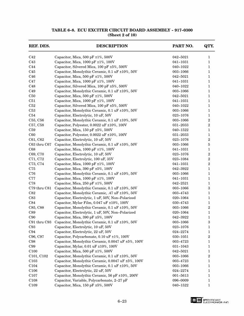
6-23
TABLE 6-8. ECU EXCITER CIRCUIT BOARD ASSEMBLY - 917-0300
(Sheet 2 of 10)
REF. DES. DESCRIPTION PART NO. QTY.
C42 Capacitor, Mica, 500 pF ±1%, 500V 042-5021 1
C43 Capacitor, Mica, 1000 pF ±1%, 100V 041-1031 1
C44 Capacitor, Silvered Mica, 100 pF ±5%, 500V 040-1022 1
C45 Capacitor, Monolythic Ceramic, 0.1 uF ±10%, 50V 003-1066 1
C46 Capacitor, Mica, 500 pF ±1%, 500V 042-5021 1
C47 Capacitor, Mica, 1000 pF ±1%, 100V 041-1031 1
C48 Capacitor, Silvered Mica, 100 pF ±5%, 500V 040-1022 1
C49 Capacitor, Monolythic Ceramic, 0.1 uF ±10%, 50V 003-1066 1
C50 Capacitor, Mica, 500 pF ±1%, 500V 042-5021 1
C51 Capacitor, Mica, 1000 pF ±1%, 100V 041-1031 1
C52 Capacitor, Silvered Mica, 100 pF ±5%, 500V 040-1022 1
C53 Capacitor, Monolythic Ceramic, 0.1 uF ±10%, 50V 003-1066 1
C54 Capacitor, Electrolytic, 10 uF, 50V 023-1076 1
C55, C56 Capacitor, Monolythic Ceramic, 0.1 uF ±10%, 50V 003-1066 2
C57, C58 Capacitor, Polyester, 0.0022 uF ±10%, 100V 031-2033 2
C59 Capacitor, Mica, 150 pF ±5%, 500V 040-1522 1
C60 Capacitor, Polyester, 0.0022 uF ±10%, 100V 031-2033 1
C61, C62 Capacitor, Electrolytic, 10 uF, 50V 023-1076 2
C63 thru C67 Capacitor, Monolythic Ceramic, 0.1 uF ±10%, 50V 003-1066 5
C68 Capacitor, Mica, 1000 pF ±1%, 100V 041-1031 1
C69, C70 Capacitor, Electrolytic, 10 uF, 50V 023-1076 2
C71, C72 Capacitor, Electrolytic, 100 uF, 35V 023-1084 2
C73, C74 Capacitor, Mica, 1000 pF ±1%, 100V 041-1031 2
C75 Capacitor, Mica, 390 pF ±5%, 100V 042-3922 1
C76 Capacitor, Monolythic Ceramic, 0.1 uF ±10%, 50V 003-1066 1
C77 Capacitor, Mica, 1000 pF ±1%, 100V 041-1031 1
C78 Capacitor, Mica, 250 pF ±1%, 500V 042-2521 1
C79 thru C81 Capacitor, Monolythic Ceramic, 0.1 uF ±10%, 50V 003-1066 3
C82 Capacitor, Monolythic Ceramic, .47 uF ±10%, 50V 003-4743 1
C83 Capacitor, Electrolytic, 1 uF, 50V, Non-Polarized 020-1064 1
C84 Capacitor, Mylar Film, 0.047 uF ±10%, 100V 030-4743 1
C85, C88 Capacitor, Monolythic Ceramic, 0.1 uF ±10%, 50V 003-1066 2
C89 Capacitor, Electrolytic, 1 uF, 50V, Non-Polarized 020-1064 1
C90 Capacitor, Mica, 390 pF ±5%, 100V 042-3922 1
C91 thru C93 Capacitor, Monolythic Ceramic, 0.1 uF ±10%, 50V 003-1066 3
C93 Capacitor, Electrolytic, 10 uF, 50V 023-1076 1
C94 Capacitor, Electrolytic, 22 uF, 50V 024-2274 1
C96, C97 Capacitor, Polycarbonate, 0.10 uF ±1%, 100V 030-1051 2
C98 Capacitor, Monolythic Ceramic, 0.0047 uF ±5%, 100V 003-4723 1
C99 Capacitor, Mylar, 0.01 uF ±10%, 100V 031-1043 1
C100 Capacitor, Mica, 500 pF ±1%, 500V 042-5021 1
C101, C102 Capacitor, Monolythic Ceramic, 0.1 uF ±10%, 50V 003-1066 2
C103 Capacitor, Monolythic Ceramic, 0.0047 uF ±5%, 100V 003-4723 1
C104 Capacitor, Monolythic Ceramic, 0.1 uF ±10%, 50V 003-1066 1
C106 Capacitor, Electrolytic, 22 uF, 50V 024-2274 1
C107 Capacitor, Monolythic Ceramic, 56 pF ±10%, 200V 001-5613 1
C108 Capacitor, Variable, Polycarbonate, 2-27 pF 096-0009 1
C109 Capacitor, Mica, 150 pF ±5%, 500V 040-1522 1
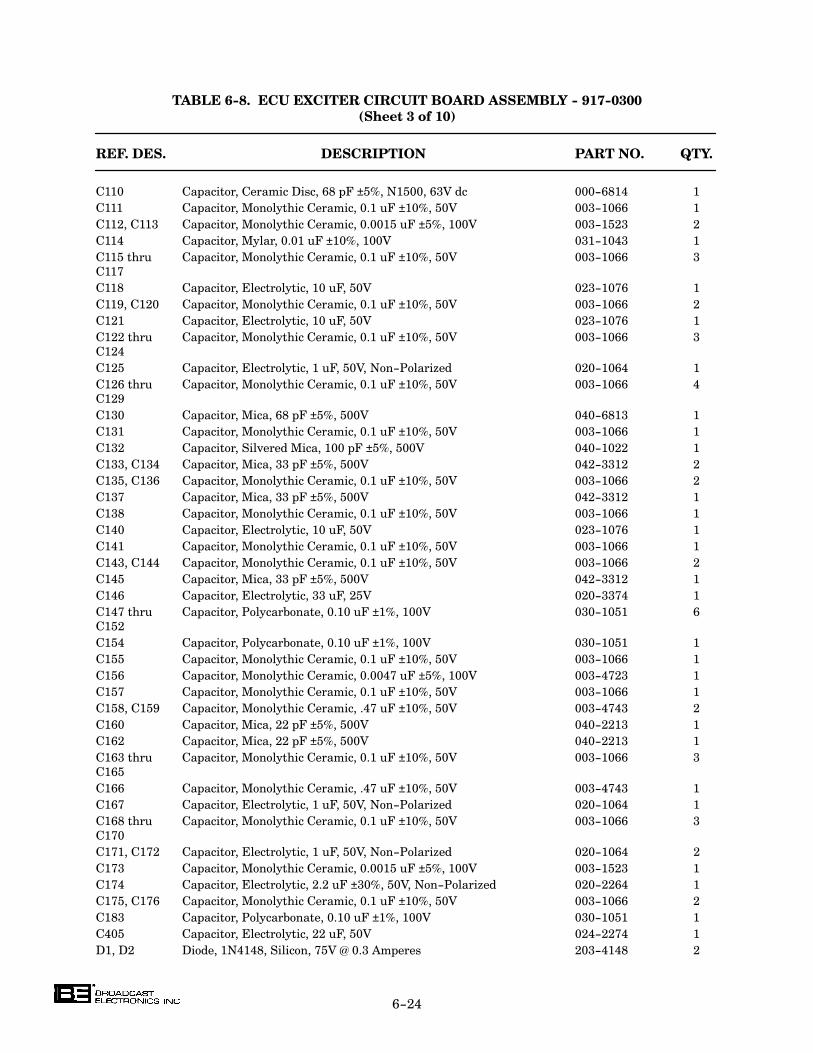
6-24
TABLE 6-8. ECU EXCITER CIRCUIT BOARD ASSEMBLY - 917-0300
(Sheet 3 of 10)
REF. DES. DESCRIPTION PART NO. QTY.
C110 Capacitor, Ceramic Disc, 68 pF ±5%, N1500, 63V dc 000-6814 1
C111 Capacitor, Monolythic Ceramic, 0.1 uF ±10%, 50V 003-1066 1
C112, C113 Capacitor, Monolythic Ceramic, 0.0015 uF ±5%, 100V 003-1523 2
C114 Capacitor, Mylar, 0.01 uF ±10%, 100V 031-1043 1
C115 thru Capacitor, Monolythic Ceramic, 0.1 uF ±10%, 50V 003-1066 3
C117
C118 Capacitor, Electrolytic, 10 uF, 50V 023-1076 1
C119, C120 Capacitor, Monolythic Ceramic, 0.1 uF ±10%, 50V 003-1066 2
C121 Capacitor, Electrolytic, 10 uF, 50V 023-1076 1
C122 thru Capacitor, Monolythic Ceramic, 0.1 uF ±10%, 50V 003-1066 3
C124
C125 Capacitor, Electrolytic, 1 uF, 50V, Non-Polarized 020-1064 1
C126 thru Capacitor, Monolythic Ceramic, 0.1 uF ±10%, 50V 003-1066 4
C129
C130 Capacitor, Mica, 68 pF ±5%, 500V 040-6813 1
C131 Capacitor, Monolythic Ceramic, 0.1 uF ±10%, 50V 003-1066 1
C132 Capacitor, Silvered Mica, 100 pF ±5%, 500V 040-1022 1
C133, C134 Capacitor, Mica, 33 pF ±5%, 500V 042-3312 2
C135, C136 Capacitor, Monolythic Ceramic, 0.1 uF ±10%, 50V 003-1066 2
C137 Capacitor, Mica, 33 pF ±5%, 500V 042-3312 1
C138 Capacitor, Monolythic Ceramic, 0.1 uF ±10%, 50V 003-1066 1
C140 Capacitor, Electrolytic, 10 uF, 50V 023-1076 1
C141 Capacitor, Monolythic Ceramic, 0.1 uF ±10%, 50V 003-1066 1
C143, C144 Capacitor, Monolythic Ceramic, 0.1 uF ±10%, 50V 003-1066 2
C145 Capacitor, Mica, 33 pF ±5%, 500V 042-3312 1
C146 Capacitor, Electrolytic, 33 uF, 25V 020-3374 1
C147 thru Capacitor, Polycarbonate, 0.10 uF ±1%, 100V 030-1051 6
C152
C154 Capacitor, Polycarbonate, 0.10 uF ±1%, 100V 030-1051 1
C155 Capacitor, Monolythic Ceramic, 0.1 uF ±10%, 50V 003-1066 1
C156 Capacitor, Monolythic Ceramic, 0.0047 uF ±5%, 100V 003-4723 1
C157 Capacitor, Monolythic Ceramic, 0.1 uF ±10%, 50V 003-1066 1
C158, C159 Capacitor, Monolythic Ceramic, .47 uF ±10%, 50V 003-4743 2
C160 Capacitor, Mica, 22 pF ±5%, 500V 040-2213 1
C162 Capacitor, Mica, 22 pF ±5%, 500V 040-2213 1
C163 thru Capacitor, Monolythic Ceramic, 0.1 uF ±10%, 50V 003-1066 3
C165
C166 Capacitor, Monolythic Ceramic, .47 uF ±10%, 50V 003-4743 1
C167 Capacitor, Electrolytic, 1 uF, 50V, Non-Polarized 020-1064 1
C168 thru Capacitor, Monolythic Ceramic, 0.1 uF ±10%, 50V 003-1066 3
C170
C171, C172 Capacitor, Electrolytic, 1 uF, 50V, Non-Polarized 020-1064 2
C173 Capacitor, Monolythic Ceramic, 0.0015 uF ±5%, 100V 003-1523 1
C174 Capacitor, Electrolytic, 2.2 uF ±30%, 50V, Non-Polarized 020-2264 1
C175, C176 Capacitor, Monolythic Ceramic, 0.1 uF ±10%, 50V 003-1066 2
C183 Capacitor, Polycarbonate, 0.10 uF ±1%, 100V 030-1051 1
C405 Capacitor, Electrolytic, 22 uF, 50V 024-2274 1
D1, D2 Diode, 1N4148, Silicon, 75V @ 0.3 Amperes 203-4148 2
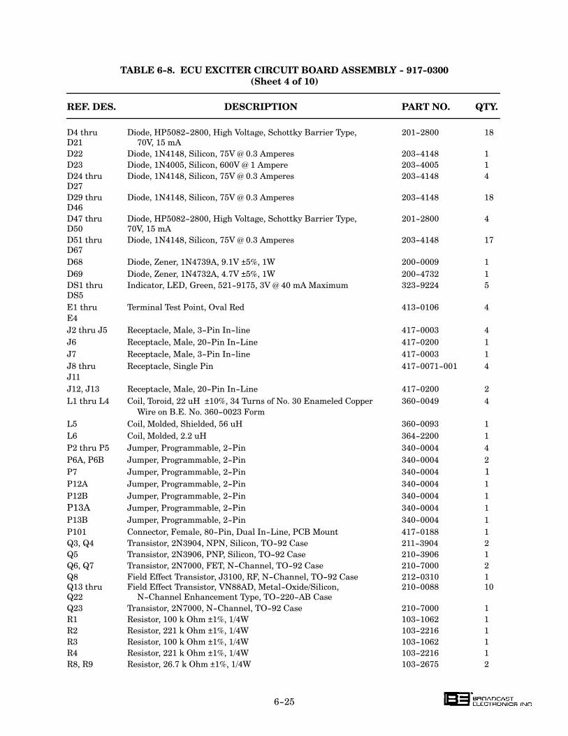
6-25
TABLE 6-8. ECU EXCITER CIRCUIT BOARD ASSEMBLY - 917-0300
(Sheet 4 of 10)
REF. DES. DESCRIPTION PART NO. QTY.
D4 thru Diode, HP5082-2800, High Voltage, Schottky Barrier Type, 201-2800 18
D21 70V, 15 mA
D22 Diode, 1N4148, Silicon, 75V @ 0.3 Amperes 203-4148 1
D23 Diode, 1N4005, Silicon, 600V @ 1 Ampere 203-4005 1
D24 thru Diode, 1N4148, Silicon, 75V @ 0.3 Amperes 203-4148 4
D27
D29 thru Diode, 1N4148, Silicon, 75V @ 0.3 Amperes 203-4148 18
D46
D47 thru Diode, HP5082-2800, High Voltage, Schottky Barrier Type, 201-2800 4
D50 70V, 15 mA
D51 thru Diode, 1N4148, Silicon, 75V @ 0.3 Amperes 203-4148 17
D67
D68 Diode, Zener, 1N4739A, 9.1V ±5%, 1W 200-0009 1
D69 Diode, Zener, 1N4732A, 4.7V ±5%, 1W 200-4732 1
DS1 thru Indicator, LED, Green, 521-9175, 3V @ 40 mA Maximum 323-9224 5
DS5
E1 thru Terminal Test Point, Oval Red 413-0106 4
E4
J2 thru J5 Receptacle, Male, 3-Pin In-line 417-0003 4
J6 Receptacle, Male, 20-Pin In-Line 417-0200 1
J7 Receptacle, Male, 3-Pin In-line 417-0003 1
J8 thru Receptacle, Single Pin 417-0071-001 4
J11
J12, J13 Receptacle, Male, 20-Pin In-Line 417-0200 2
L1 thru L4 Coil, Toroid, 22 uH ±10%, 34 Turns of No. 30 Enameled Copper 360-0049 4
Wire on B.E. No. 360-0023 Form
L5 Coil, Molded, Shielded, 56 uH 360-0093 1
L6 Coil, Molded, 2.2 uH 364-2200 1
P2 thru P5 Jumper, Programmable, 2-Pin 340-0004 4
P6A, P6B Jumper, Programmable, 2-Pin 340-0004 2
P7 Jumper, Programmable, 2-Pin 340-0004 1
P12A Jumper, Programmable, 2-Pin 340-0004 1
P12B Jumper, Programmable, 2-Pin 340-0004 1
P13A Jumper, Programmable, 2-Pin 340-0004 1
P13B Jumper, Programmable, 2-Pin 340-0004 1
P101 Connector, Female, 80-Pin, Dual In-Line, PCB Mount 417-0188 1
Q3, Q4 Transistor, 2N3904, NPN, Silicon, TO-92 Case 211-3904 2
Q5 Transistor, 2N3906, PNP, Silicon, TO-92 Case 210-3906 1
Q6, Q7 Transistor, 2N7000, FET, N-Channel, TO-92 Case 210-7000 2
Q8 Field Effect Transistor, J3100, RF, N-Channel, TO-92 Case 212-0310 1
Q13 thru Field Effect Transistor, VN88AD, Metal-Oxide/Silicon, 210-0088 10
Q22 N-Channel Enhancement Type, TO-220-AB Case
Q23 Transistor, 2N7000, N-Channel, TO-92 Case 210-7000 1
R1 Resistor, 100 k Ohm ±1%, 1/4W 103-1062 1
R2 Resistor, 221 k Ohm ±1%, 1/4W 103-2216 1
R3 Resistor, 100 k Ohm ±1%, 1/4W 103-1062 1
R4 Resistor, 221 k Ohm ±1%, 1/4W 103-2216 1
R8, R9 Resistor, 26.7 k Ohm ±1%, 1/4W 103-2675 2
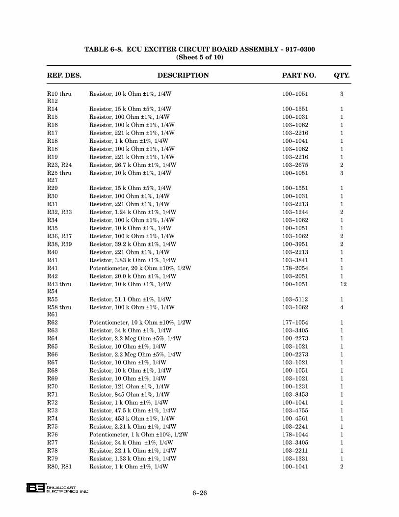
6-26
TABLE 6-8. ECU EXCITER CIRCUIT BOARD ASSEMBLY - 917-0300
(Sheet 5 of 10)
REF. DES. DESCRIPTION PART NO. QTY.
R10 thru Resistor, 10 k Ohm ±1%, 1/4W 100-1051 3
R12
R14 Resistor, 15 k Ohm ±5%, 1/4W 100-1551 1
R15 Resistor, 100 Ohm ±1%, 1/4W 100-1031 1
R16 Resistor, 100 k Ohm ±1%, 1/4W 103-1062 1
R17 Resistor, 221 k Ohm ±1%, 1/4W 103-2216 1
R18 Resistor, 1 k Ohm ±1%, 1/4W 100-1041 1
R18 Resistor, 100 k Ohm ±1%, 1/4W 103-1062 1
R19 Resistor, 221 k Ohm ±1%, 1/4W 103-2216 1
R23, R24 Resistor, 26.7 k Ohm ±1%, 1/4W 103-2675 2
R25 thru Resistor, 10 k Ohm ±1%, 1/4W 100-1051 3
R27
R29 Resistor, 15 k Ohm ±5%, 1/4W 100-1551 1
R30 Resistor, 100 Ohm ±1%, 1/4W 100-1031 1
R31 Resistor, 221 Ohm ±1%, 1/4W 103-2213 1
R32, R33 Resistor, 1.24 k Ohm ±1%, 1/4W 103-1244 2
R34 Resistor, 100 k Ohm ±1%, 1/4W 103-1062 1
R35 Resistor, 10 k Ohm ±1%, 1/4W 100-1051 1
R36, R37 Resistor, 100 k Ohm ±1%, 1/4W 103-1062 2
R38, R39 Resistor, 39.2 k Ohm ±1%, 1/4W 100-3951 2
R40 Resistor, 221 Ohm ±1%, 1/4W 103-2213 1
R41 Resistor, 3.83 k Ohm ±1%, 1/4W 103-3841 1
R41 Potentiometer, 20 k Ohm ±10%, 1/2W 178-2054 1
R42 Resistor, 20.0 k Ohm ±1%, 1/4W 103-2051 1
R43 thru Resistor, 10 k Ohm ±1%, 1/4W 100-1051 12
R54
R55 Resistor, 51.1 Ohm ±1%, 1/4W 103-5112 1
R58 thru Resistor, 100 k Ohm ±1%, 1/4W 103-1062 4
R61
R62 Potentiometer, 10 k Ohm ±10%, 1/2W 177-1054 1
R63 Resistor, 34 k Ohm ±1%, 1/4W 103-3405 1
R64 Resistor, 2.2 Meg Ohm ±5%, 1/4W 100-2273 1
R65 Resistor, 10 Ohm ±1%, 1/4W 103-1021 1
R66 Resistor, 2.2 Meg Ohm ±5%, 1/4W 100-2273 1
R67 Resistor, 10 Ohm ±1%, 1/4W 103-1021 1
R68 Resistor, 10 k Ohm ±1%, 1/4W 100-1051 1
R69 Resistor, 10 Ohm ±1%, 1/4W 103-1021 1
R70 Resistor, 121 Ohm ±1%, 1/4W 100-1231 1
R71 Resistor, 845 Ohm ±1%, 1/4W 103-8453 1
R72 Resistor, 1 k Ohm ±1%, 1/4W 100-1041 1
R73 Resistor, 47.5 k Ohm ±1%, 1/4W 103-4755 1
R74 Resistor, 453 k Ohm ±1%, 1/4W 100-4561 1
R75 Resistor, 2.21 k Ohm ±1%, 1/4W 103-2241 1
R76 Potentiometer, 1 k Ohm ±10%, 1/2W 178-1044 1
R77 Resistor, 34 k Ohm ±1%, 1/4W 103-3405 1
R78 Resistor, 22.1 k Ohm ±1%, 1/4W 103-2211 1
R79 Resistor, 1.33 k Ohm ±1%, 1/4W 103-1331 1
R80, R81 Resistor, 1 k Ohm ±1%, 1/4W 100-1041 2
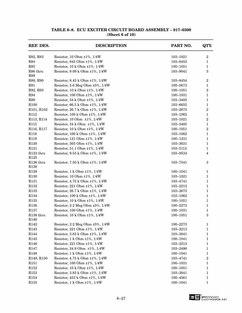
6-27
TABLE 6-8. ECU EXCITER CIRCUIT BOARD ASSEMBLY - 917-0300
(Sheet 6 of 10)
REF. DES. DESCRIPTION PART NO. QTY.
R82, R83 Resistor, 10 Ohm ±1%, 1/4W 103-1021 2
R84 Resistor, 845 Ohm ±1%, 1/4W 103-8453 1
R85 Resistor, 10 k Ohm ±1%, 1/4W 100-1051 1
R86 thru Resistor, 9.09 k Ohm ±1%, 1/4W 103-9041 3
R88
R89, R90 Resistor, 8.45 k Ohm ±1%, 1/4W 103-8454 2
R91 Resistor, 5.6 Meg Ohm ±5%, 1/4W 100-5673 1
R92, R93 Resistor, 10 k Ohm ±1%, 1/4W 100-1051 2
R94 Resistor, 100 Ohm ±1%, 1/4W 100-1031 1
R99 Resistor, 34 k Ohm ±1%, 1/4W 103-3405 1
R100 Resistor, 66.5 k Ohm ±1%, 1/4W 103-6655 1
R101, R102 Resistor, 26.7 k Ohm ±1%, 1/4W 103-2675 2
R112 Resistor, 100 k Ohm ±1%, 1/4W 103-1062 1
R113, R114 Resistor, 10 Ohm ±1%, 1/4W 103-1021 2
R115 Resistor, 34 k Ohm ±1%, 1/4W 103-3405 1
R116, R117 Resistor, 10 k Ohm ±1%, 1/4W 100-1051 2
R118 Resistor, 100 k Ohm ±1%, 1/4W 103-1062 1
R119 Resistor, 121 Ohm ±1%, 1/4W 100-1231 1
R120 Resistor, 365 Ohm ±1%, 1/4W 103-3631 1
R121 Resistor, 51.1 Ohm ±1%, 1/4W 103-5112 1
R122 thru Resistor, 9.53 k Ohm ±1%, 1/4W 103-9534 4
R125
R126 thru Resistor, 7.50 k Ohm ±1%, 1/4W 103-7541 3
R128
R129 Resistor, 1 k Ohm ±1%, 1/4W 100-1041 1
R130 Resistor, 10 Ohm ±1%, 1/4W 103-1021 1
R131 Resistor, 4.75 k Ohm ±1%, 1/4W 103-4741 1
R132 Resistor, 221 Ohm ±1%, 1/4W 103-2213 1
R133 Resistor, 26.7 k Ohm ±1%, 1/4W 103-2675 1
R134 Resistor, 100 k Ohm ±1%, 1/4W 103-1062 1
R135 Resistor, 10 k Ohm ±1%, 1/4W 100-1051 1
R136 Resistor, 2.2 Meg Ohm ±5%, 1/4W 100-2273 1
R137 Resistor, 100 Ohm ±1%, 1/4W 100-1031 1
R138 thru Resistor, 10 k Ohm ±1%, 1/4W 100-1051 3
R140
R142 Resistor, 2.2 Meg Ohm ±5%, 1/4W 100-2273 1
R143 Resistor, 221 Ohm ±1%, 1/4W 103-2213 1
R144 Resistor, 3.83 k Ohm ±1%, 1/4W 103-3841 1
R145 Resistor, 1 k Ohm ±1%, 1/4W 100-1041 1
R146 Resistor, 221 Ohm ±1%, 1/4W 103-2213 1
R147 Resistor, 24.9 Ohm ±1%, 1/4W 103-2490 1
R148 Resistor, 1 k Ohm ±1%, 1/4W 100-1041 1
R149, R150 Resistor, 4.75 k Ohm ±1%, 1/4W 103-4741 2
R151 Resistor, 100 Ohm ±1%, 1/4W 100-1031 1
R152 Resistor, 10 k Ohm ±1%, 1/4W 100-1051 1
R153 Resistor, 3.83 k Ohm ±1%, 1/4W 103-3841 1
R154 Resistor, 453 k Ohm ±1%, 1/4W 100-4561 1
R155 Resistor, 1 k Ohm ±1%, 1/4W 100-1041 1
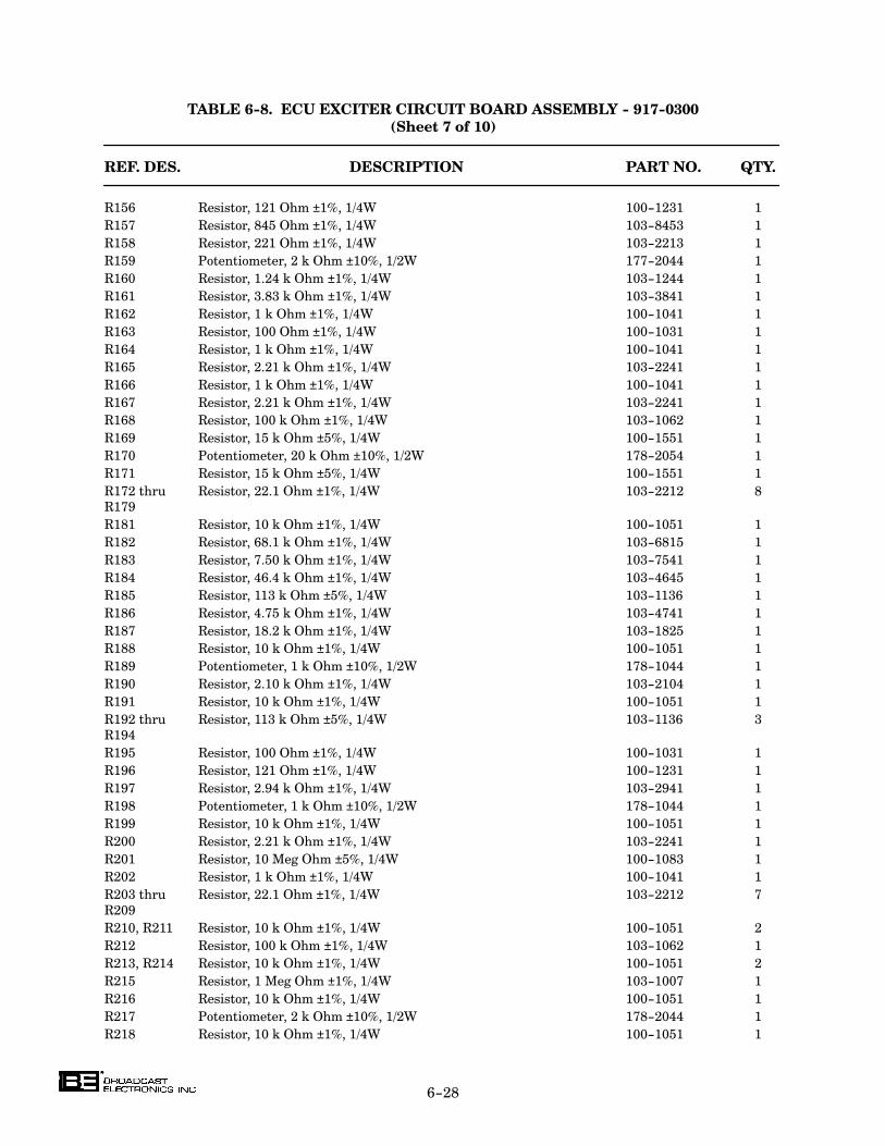
6-28
TABLE 6-8. ECU EXCITER CIRCUIT BOARD ASSEMBLY - 917-0300
(Sheet 7 of 10)
REF. DES. DESCRIPTION PART NO. QTY.
R156 Resistor, 121 Ohm ±1%, 1/4W 100-1231 1
R157 Resistor, 845 Ohm ±1%, 1/4W 103-8453 1
R158 Resistor, 221 Ohm ±1%, 1/4W 103-2213 1
R159 Potentiometer, 2 k Ohm ±10%, 1/2W 177-2044 1
R160 Resistor, 1.24 k Ohm ±1%, 1/4W 103-1244 1
R161 Resistor, 3.83 k Ohm ±1%, 1/4W 103-3841 1
R162 Resistor, 1 k Ohm ±1%, 1/4W 100-1041 1
R163 Resistor, 100 Ohm ±1%, 1/4W 100-1031 1
R164 Resistor, 1 k Ohm ±1%, 1/4W 100-1041 1
R165 Resistor, 2.21 k Ohm ±1%, 1/4W 103-2241 1
R166 Resistor, 1 k Ohm ±1%, 1/4W 100-1041 1
R167 Resistor, 2.21 k Ohm ±1%, 1/4W 103-2241 1
R168 Resistor, 100 k Ohm ±1%, 1/4W 103-1062 1
R169 Resistor, 15 k Ohm ±5%, 1/4W 100-1551 1
R170 Potentiometer, 20 k Ohm ±10%, 1/2W 178-2054 1
R171 Resistor, 15 k Ohm ±5%, 1/4W 100-1551 1
R172 thru Resistor, 22.1 Ohm ±1%, 1/4W 103-2212 8
R179
R181 Resistor, 10 k Ohm ±1%, 1/4W 100-1051 1
R182 Resistor, 68.1 k Ohm ±1%, 1/4W 103-6815 1
R183 Resistor, 7.50 k Ohm ±1%, 1/4W 103-7541 1
R184 Resistor, 46.4 k Ohm ±1%, 1/4W 103-4645 1
R185 Resistor, 113 k Ohm ±5%, 1/4W 103-1136 1
R186 Resistor, 4.75 k Ohm ±1%, 1/4W 103-4741 1
R187 Resistor, 18.2 k Ohm ±1%, 1/4W 103-1825 1
R188 Resistor, 10 k Ohm ±1%, 1/4W 100-1051 1
R189 Potentiometer, 1 k Ohm ±10%, 1/2W 178-1044 1
R190 Resistor, 2.10 k Ohm ±1%, 1/4W 103-2104 1
R191 Resistor, 10 k Ohm ±1%, 1/4W 100-1051 1
R192 thru Resistor, 113 k Ohm ±5%, 1/4W 103-1136 3
R194
R195 Resistor, 100 Ohm ±1%, 1/4W 100-1031 1
R196 Resistor, 121 Ohm ±1%, 1/4W 100-1231 1
R197 Resistor, 2.94 k Ohm ±1%, 1/4W 103-2941 1
R198 Potentiometer, 1 k Ohm ±10%, 1/2W 178-1044 1
R199 Resistor, 10 k Ohm ±1%, 1/4W 100-1051 1
R200 Resistor, 2.21 k Ohm ±1%, 1/4W 103-2241 1
R201 Resistor, 10 Meg Ohm ±5%, 1/4W 100-1083 1
R202 Resistor, 1 k Ohm ±1%, 1/4W 100-1041 1
R203 thru Resistor, 22.1 Ohm ±1%, 1/4W 103-2212 7
R209
R210, R211 Resistor, 10 k Ohm ±1%, 1/4W 100-1051 2
R212 Resistor, 100 k Ohm ±1%, 1/4W 103-1062 1
R213, R214 Resistor, 10 k Ohm ±1%, 1/4W 100-1051 2
R215 Resistor, 1 Meg Ohm ±1%, 1/4W 103-1007 1
R216 Resistor, 10 k Ohm ±1%, 1/4W 100-1051 1
R217 Potentiometer, 2 k Ohm ±10%, 1/2W 178-2044 1
R218 Resistor, 10 k Ohm ±1%, 1/4W 100-1051 1
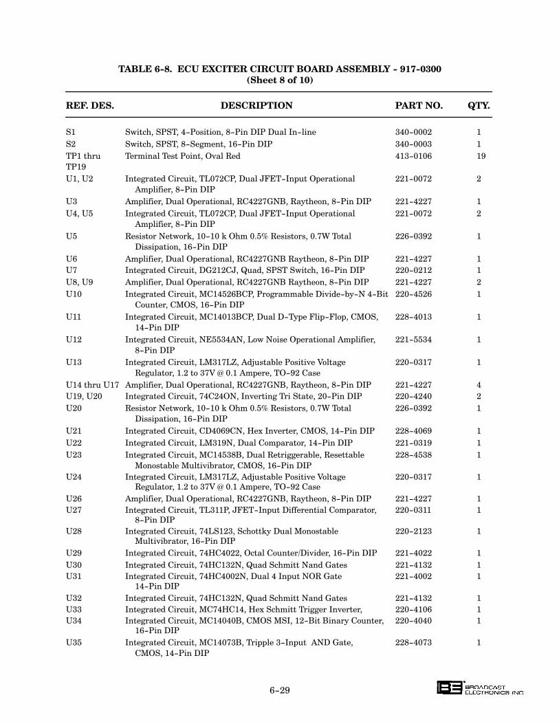
6-29
TABLE 6-8. ECU EXCITER CIRCUIT BOARD ASSEMBLY - 917-0300
(Sheet 8 of 10)
REF. DES. DESCRIPTION PART NO. QTY.
S1 Switch, SPST, 4-Position, 8-Pin DIP Dual In-line 340-0002 1
S2 Switch, SPST, 8-Segment, 16-Pin DIP 340-0003 1
TP1 thru Terminal Test Point, Oval Red 413-0106 19
TP19
U1, U2 Integrated Circuit, TL072CP, Dual JFET-Input Operational 221-0072 2
Amplifier, 8-Pin DIP
U3 Amplifier, Dual Operational, RC4227GNB, Raytheon, 8-Pin DIP 221-4227 1
U4, U5 Integrated Circuit, TL072CP, Dual JFET-Input Operational 221-0072 2
Amplifier, 8-Pin DIP
U5 Resistor Network, 10-10 k Ohm 0.5% Resistors, 0.7W Total 226-0392 1
Dissipation, 16-Pin DIP
U6 Amplifier, Dual Operational, RC4227GNB Raytheon, 8-Pin DIP 221-4227 1
U7 Integrated Circuit, DG212CJ, Quad, SPST Switch, 16-Pin DIP 220-0212 1
U8, U9 Amplifier, Dual Operational, RC4227GNB Raytheon, 8-Pin DIP 221-4227 2
U10 Integrated Circuit, MC14526BCP, Programmable Divide-by-N 4-Bit 220-4526 1
Counter, CMOS, 16-Pin DIP
U11 Integrated Circuit, MC14013BCP, Dual D-Type Flip-Flop, CMOS, 228-4013 1
14-Pin DIP
U12 Integrated Circuit, NE5534AN, Low Noise Operational Amplifier, 221-5534 1
8-Pin DIP
U13 Integrated Circuit, LM317LZ, Adjustable Positive Voltage 220-0317 1
Regulator, 1.2 to 37V @ 0.1 Ampere, TO-92 Case
U14 thru U17 Amplifier, Dual Operational, RC4227GNB, Raytheon, 8-Pin DIP 221-4227 4
U19, U20 Integrated Circuit, 74C24ON, Inverting Tri State, 20-Pin DIP 220-4240 2
U20 Resistor Network, 10-10 k Ohm 0.5% Resistors, 0.7W Total 226-0392 1
Dissipation, 16-Pin DIP
U21 Integrated Circuit, CD4069CN, Hex Inverter, CMOS, 14-Pin DIP 228-4069 1
U22 Integrated Circuit, LM319N, Dual Comparator, 14-Pin DIP 221-0319 1
U23 Integrated Circuit, MC14538B, Dual Retriggerable, Resettable 228-4538 1
Monostable Multivibrator, CMOS, 16-Pin DIP
U24 Integrated Circuit, LM317LZ, Adjustable Positive Voltage 220-0317 1
Regulator, 1.2 to 37V @ 0.1 Ampere, TO-92 Case
U26 Amplifier, Dual Operational, RC4227GNB, Raytheon, 8-Pin DIP 221-4227 1
U27 Integrated Circuit, TL311P, JFET-Input Differential Comparator, 220-0311 1
8-Pin DIP
U28 Integrated Circuit, 74LS123, Schottky Dual Monostable 220-2123 1
Multivibrator, 16-Pin DIP
U29 Integrated Circuit, 74HC4022, Octal Counter/Divider, 16-Pin DIP 221-4022 1
U30 Integrated Circuit, 74HC132N, Quad Schmitt Nand Gates 221-4132 1
U31 Integrated Circuit, 74HC4002N, Dual 4 Input NOR Gate 221-4002 1
14-Pin DIP
U32 Integrated Circuit, 74HC132N, Quad Schmitt Nand Gates 221-4132 1
U33 Integrated Circuit, MC74HC14, Hex Schmitt Trigger Inverter, 220-4106 1
U34 Integrated Circuit, MC14040B, CMOS MSI, 12-Bit Binary Counter, 220-4040 1
16-Pin DIP
U35 Integrated Circuit, MC14073B, Tripple 3-Input AND Gate, 228-4073 1
CMOS, 14-Pin DIP

6-30
TABLE 6-8. ECU EXCITER CIRCUIT BOARD ASSEMBLY - 917-0300
(Sheet 9 of 10)
REF. DES. DESCRIPTION PART NO. QTY.
U36 Integrated Circuit, MC14013BCP, Dual D-Type Flip-Flop, CMOS, 228-4013 1
14-Pin DIP
U37 Integrated Circuit, LM317LZ, Adjustable Positive Voltage 220-0317 1
Regulator, 1.2 to 37V @ 0.1 Ampere, TO-92 Case
U38, U39 Integrated Circuit, 74HC132N QUAD Schmitt Nand Gates 221-4132 2
U40 Integrated Circuit, 74HC75N, Quad D Latch 221-7475 1
U41 Amplifier, Dual Operational, RC4227GNB, Raytheon, 8-Pin DIP 221-4227 1
U42 Integrated Circuit, 74HC74N Dual D Flip Flop 221-7474 1
U43 Integrated Circuit, TL311P, JFET-Input Differential Comparator, 220-0311 1
8-Pin DIP
U44 Integrated Circuit, MC14060B, 14-Bit Binary Counter and 220-4060 1
Oscillator, CMOS MSI, 16-Pin DIP
U45 Integrated Circuit, 74C24ON, Inverting Tri State, 20-Pin DIP 220-4240 1
U46 Driver, High and Low Side, IR2112, 14-Pin DIP 227-2112 1
U47 Integrated Circuit, LM319N, Dual Comparator, 14-Pin DIP 221-0319 1
XU1 thru Socket, 8-Pin DIP 417-0804 6
XU6
XU4 Socket, 14-Pin DIP 417-1404 1
XU7 Socket, 16-Pin DIP 417-1604 1
XU8, XU9 Socket, 8-Pin DIP 417-0804 2
XU10 Socket, 16-Pin DIP 417-1604 1
XU11 Socket, 14-Pin DIP 417-1404 1
XU12 Socket, 8-Pin DIP 417-0804 1
XU14 thru Socket, 8-Pin DIP 417-0804 4
XU17
XU19, XU20 Socket, 20-Pin DIP 417-2004 2
XU21, XU22 Socket, 14-Pin DIP 417-1404 2
XU23 Socket, 16-Pin DIP 417-1604 1
XU25 Receptacle, 28-Pin DIP 417-2804 1
XU26, XU27 Socket, 8-Pin DIP 417-0804 2
XU28 Socket, 16-Pin DIP 417-1604 1
XU29 Socket, 16-Pin DIP 417-1604 1
XU30 thru Socket, 14-Pin DIP 417-1404 4
XU33
XU34 Socket, 16-Pin DIP 417-1604 1
XU35, XU36 Socket, 14-Pin DIP 417-1404 2
XU38, XU39 Socket, 14-Pin DIP 417-1404 2
XU40 Socket, 16-Pin DIP 417-1604 1
XU41 Socket, 8-Pin DIP 417-0804 1
XU42 Socket, 14-Pin DIP 417-1404 1
XU43 Socket, 8-Pin DIP 417-0804 1
XU44 Socket, 16-Pin DIP 417-1604 1
XU45 Socket, 20-Pin DIP 417-2004 1
XU46, XU47 Socket, 14-Pin DIP 417-1404 2
10 kHz SPACING
Y1 Crystal, 48PD1002, 10.24 MHz, HC-18 Cinox 390-0013 1

6-31
TABLE 6-8. ECU EXCITER CIRCUIT BOARD ASSEMBLY - 917-0300
(Sheet 10 of 10)
REF. DES. DESCRIPTION PART NO. QTY.
9 kHz SPACING
Y1 Crystal, 9.216 MHz, HC-18 Cinox 390-0017 1
---- Integrated Circuit, MC145151P, Parallel Input, PLL 220-5151 1
Frequency Synthesizer, CMOS, 28-Pin DIP
---- Blank, ECU Exciter Circuit Board 517-0300 1
---- VCO Module Circuit Board Assembly 917-0069 1
TABLE 6-9. VCO MODULE CIRCUIT BOARD ASSEMBLY - 917-0069
REF. DES. DESCRIPTION PART NO. QTY.
C1, C2 Capacitor, Monolythic Ceramic, 0.01 uF ±5%, 100V 003-1013 2
C3 Capacitor, Monolythic Ceramic, 0.1 uF ±20%, 50V 003-1054 1
C4 Capacitor, Mica, 50 pF ±5%, 500V 040-5013 1
C5 Capacitor, Monolythic Ceramic, 0.1 uF ±20%, 50V 003-1054 1
D1 Diode, Varactor, MVAM115, 500 pF at 1 VR, 25 pF at 15 VR, 200-0115 1
Motorola Case 182-03
D2, D3 Diode, 1N4148, Silicon, 75V @ 0.3 Amperes 203-4148 2
P32 thru Plug, Male, Single Pin 417-0119 4
P35
Q1, Q2 Field Effect Transistor, J3100, RF, N-Channel, TO-92 Case 212-0310 2
R1 Resistor, 619 Ohm ±1%, 1/4W 103-6193 1
R2 Resistor, 100 Ohm ±1%, 1/4W 100-1031 1
R3 Resistor, 475 Ohm ±1%, 1/4W 103-4753 1
R4 Resistor, 100 k Ohm ±1%, 1/4W 103-1062 1
R5 Resistor, 100 Ohm ±1%, 1/4W 100-1031 1
R6 Resistor, 475 Ohm ±1%, 1/4W 103-4753 1
---- Ferrite Toroid, OD = 0.375 IN, ID = 0.188 IN, W = 0.125 IN 360-0023 1
---- Blank, VCO Module Circuit Board 517-0069 1
TABLE 6-10. ECU MOTHERBOARD CIRCUIT BOARD ASSEMBLY - 917-0301
(Sheet 1 of 3)
REF. DES. DESCRIPTION PART NO. QTY.
C1, C2 Capacitor, Polyester, 0.0022 uF ±10%, 100V 031-2033 2
C3, C4 Capacitor, Polyester, 0.015 uF ±10%, 100V 030-1532 2
C5, C6 Capacitor, Polyester, 0.0022 uF ±10%, 100V 031-2033 2
C7, C8 Capacitor, Polyester, 0.015 uF ±10%, 100V 030-1532 2
C9 thru Capacitor, Monolythic Ceramic, 0.1 uF ±10%, 50V 003-1066 51
C59
C61 thru Capacitor, Monolythic Ceramic, 0.1 uF ±10%, 50V 003-1066 5
C65
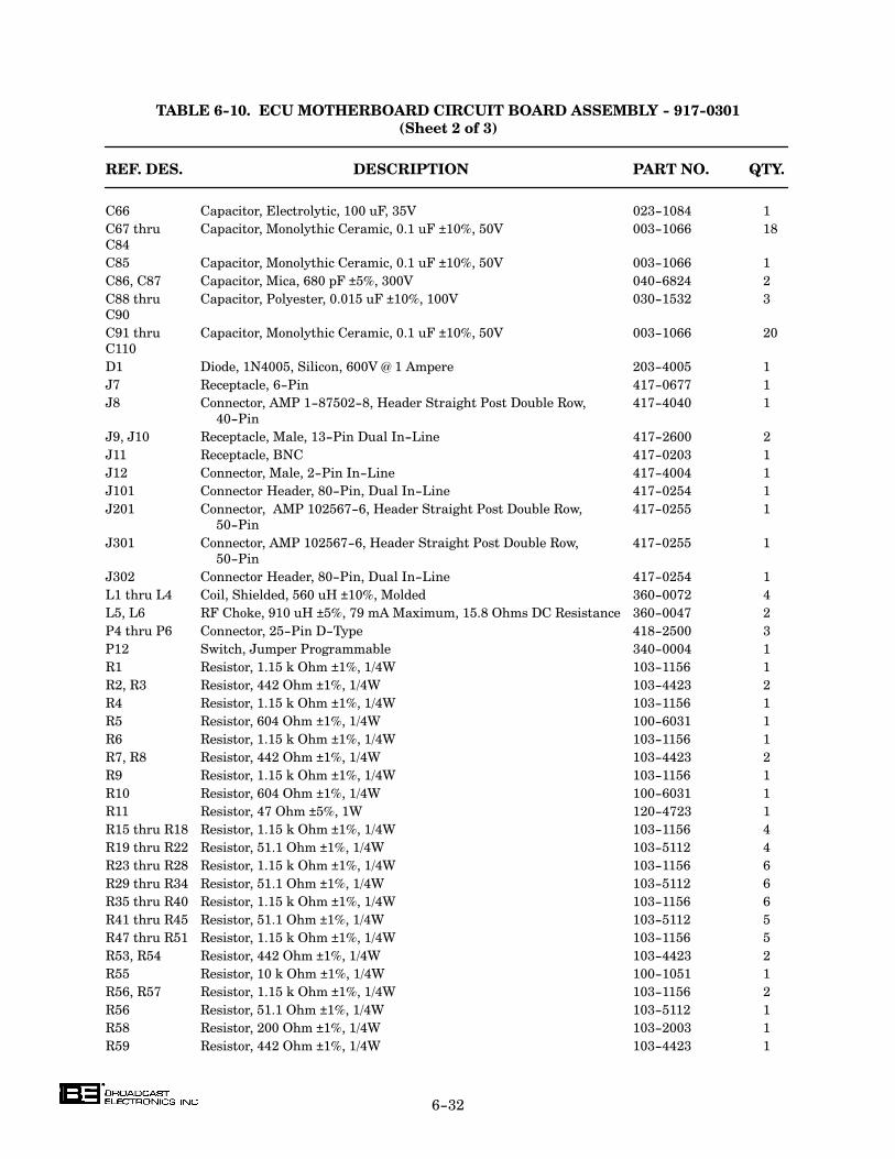
6-32
TABLE 6-10. ECU MOTHERBOARD CIRCUIT BOARD ASSEMBLY - 917-0301
(Sheet 2 of 3)
REF. DES. DESCRIPTION PART NO. QTY.
C66 Capacitor, Electrolytic, 100 uF, 35V 023-1084 1
C67 thru Capacitor, Monolythic Ceramic, 0.1 uF ±10%, 50V 003-1066 18
C84
C85 Capacitor, Monolythic Ceramic, 0.1 uF ±10%, 50V 003-1066 1
C86, C87 Capacitor, Mica, 680 pF ±5%, 300V 040-6824 2
C88 thru Capacitor, Polyester, 0.015 uF ±10%, 100V 030-1532 3
C90
C91 thru Capacitor, Monolythic Ceramic, 0.1 uF ±10%, 50V 003-1066 20
C110
D1 Diode, 1N4005, Silicon, 600V @ 1 Ampere 203-4005 1
J7 Receptacle, 6-Pin 417-0677 1
J8 Connector, AMP 1-87502-8, Header Straight Post Double Row, 417-4040 1
40-Pin
J9, J10 Receptacle, Male, 13-Pin Dual In-Line 417-2600 2
J11 Receptacle, BNC 417-0203 1
J12 Connector, Male, 2-Pin In-Line 417-4004 1
J101 Connector Header, 80-Pin, Dual In-Line 417-0254 1
J201 Connector, AMP 102567-6, Header Straight Post Double Row, 417-0255 1
50-Pin
J301 Connector, AMP 102567-6, Header Straight Post Double Row, 417-0255 1
50-Pin
J302 Connector Header, 80-Pin, Dual In-Line 417-0254 1
L1 thru L4 Coil, Shielded, 560 uH ±10%, Molded 360-0072 4
L5, L6 RF Choke, 910 uH ±5%, 79 mA Maximum, 15.8 Ohms DC Resistance 360-0047 2
P4 thru P6 Connector, 25-Pin D-Type 418-2500 3
P12 Switch, Jumper Programmable 340-0004 1
R1 Resistor, 1.15 k Ohm ±1%, 1/4W 103-1156 1
R2, R3 Resistor, 442 Ohm ±1%, 1/4W 103-4423 2
R4 Resistor, 1.15 k Ohm ±1%, 1/4W 103-1156 1
R5 Resistor, 604 Ohm ±1%, 1/4W 100-6031 1
R6 Resistor, 1.15 k Ohm ±1%, 1/4W 103-1156 1
R7, R8 Resistor, 442 Ohm ±1%, 1/4W 103-4423 2
R9 Resistor, 1.15 k Ohm ±1%, 1/4W 103-1156 1
R10 Resistor, 604 Ohm ±1%, 1/4W 100-6031 1
R11 Resistor, 47 Ohm ±5%, 1W 120-4723 1
R15 thru R18 Resistor, 1.15 k Ohm ±1%, 1/4W 103-1156 4
R19 thru R22 Resistor, 51.1 Ohm ±1%, 1/4W 103-5112 4
R23 thru R28 Resistor, 1.15 k Ohm ±1%, 1/4W 103-1156 6
R29 thru R34 Resistor, 51.1 Ohm ±1%, 1/4W 103-5112 6
R35 thru R40 Resistor, 1.15 k Ohm ±1%, 1/4W 103-1156 6
R41 thru R45 Resistor, 51.1 Ohm ±1%, 1/4W 103-5112 5
R47 thru R51 Resistor, 1.15 k Ohm ±1%, 1/4W 103-1156 5
R53, R54 Resistor, 442 Ohm ±1%, 1/4W 103-4423 2
R55 Resistor, 10 k Ohm ±1%, 1/4W 100-1051 1
R56, R57 Resistor, 1.15 k Ohm ±1%, 1/4W 103-1156 2
R56 Resistor, 51.1 Ohm ±1%, 1/4W 103-5112 1
R58 Resistor, 200 Ohm ±1%, 1/4W 103-2003 1
R59 Resistor, 442 Ohm ±1%, 1/4W 103-4423 1
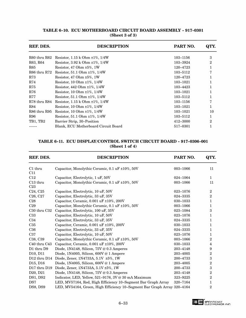
6-33
TABLE 6-10. ECU MOTHERBOARD CIRCUIT BOARD ASSEMBLY - 917-0301
(Sheet 3 of 3)
REF. DES. DESCRIPTION PART NO. QTY.
R60 thru R62 Resistor, 1.15 k Ohm ±1%, 1/4W 103-1156 3
R63, R64 Resistor, 3.92 k Ohm ±1%, 1/4W 103-3924 2
R65 Resistor, 47 Ohm ±5%, 1W 120-4723 1
R66 thru R72 Resistor, 51.1 Ohm ±1%, 1/4W 103-5112 7
R73 Resistor, 47 Ohm ±5%, 1W 120-4723 1
R74 Resistor, 10 Ohm ±1%, 1/4W 103-1021 1
R75 Resistor, 442 Ohm ±1%, 1/4W 103-4423 1
R76 Resistor, 10 Ohm ±1%, 1/4W 103-1021 1
R77 Resistor, 51.1 Ohm ±1%, 1/4W 103-5112 1
R78 thru R84 Resistor, 1.15 k Ohm ±1%, 1/4W 103-1156 7
R84 Resistor, 10 Ohm ±1%, 1/4W 103-1021 1
R86 thru R95 Resistor, 10 Ohm ±1%, 1/4W 103-1021 10
R96 Resistor, 51.1 Ohm ±1%, 1/4W 103-5112 1
TB1, TB2 Barrier Strip, 30-Position 412-3000 2
---- Blank, ECU Motherboard Circuit Board 517-0301 1
TABLE 6-11. ECU DISPLAY/CONTROL SWITCH CIRCUIT BOARD - 917-0306-001
(Sheet 1 of 4)
REF. DES. DESCRIPTION PART NO. QTY.
C1 thru Capacitor, Monolythic Ceramic, 0.1 uF ±10%, 50V 003-1066 11C11
C12 Capacitor, Electrolytic, 1 uF, 50V 024-1064 1
C13 thru Capacitor, Monolythic Ceramic, 0.1 uF ±10%, 50V 003-1066 11C23
C24, C25 Capacitor, Electrolytic, 10 uF, 50V 023-1076 2
C26, C27 Capacitor, Electrolytic, 33 uF, 35V 024-3335 2
C28 Capacitor, Ceramic, 0.001 uF ±10%, 200V 030-1033 1
C29 Capacitor, Monolythic Ceramic, 0.1 uF ±10%, 50V 003-1066 1
C30 thru C32 Capacitor, Electrolytic, 100 uF, 35V 023-1084 3
C33 Capacitor, Electrolytic, 10 uF, 50V 023-1076 1
C34 Capacitor, Electrolytic, 33 uF, 35V 024-3335 1
C35 Capacitor, Ceramic, 0.001 uF ±10%, 200V 030-1033 1
C36 Capacitor, Electrolytic, 33 uF, 35V 024-3335 1
C37 Capacitor, Electrolytic, 10 uF, 50V 023-1076 1
C38, C39 Capacitor, Monolythic Ceramic, 0.1 uF ±10%, 50V 003-1066 2
C40 thru C43 Capacitor, Ceramic, 0.001 uF ±10%, 200V 030-1033 4
D1 thru D9 Diode, 1N4148, Silicon, 75V @ 0.3 Amperes 203-4148 9
D10, D11 Diode, 1N4005, Silicon, 600V @ 1 Ampere 203-4005 2
D12 thru D14 Diode, Zener, 1N4733A, 5.1V ±5%, 1W 200-4733 3
D15, D16 Diode, 1N4005, Silicon, 600V @ 1 Ampere 203-4005 2
D17 thru D19 Diode, Zener, 1N4733A, 5.1V ±5%, 1W 200-4733 3
D20, D21 Diode, 1N4148, Silicon, 75V @ 0.3 Amperes 203-4148 2
DS1, DS2 Indicator, LED, Yellow, 521-9176, 3V @ 30 mA Maximum 323-9225 2
DS7 LED, MV57164, Red, High Efficiency 10-Segment Bar Graph Array 320-7164 1
DS8, DS9 LED, MV54164, Green, High Efficiency 10-Segment Bar Graph Array 320-4164 2
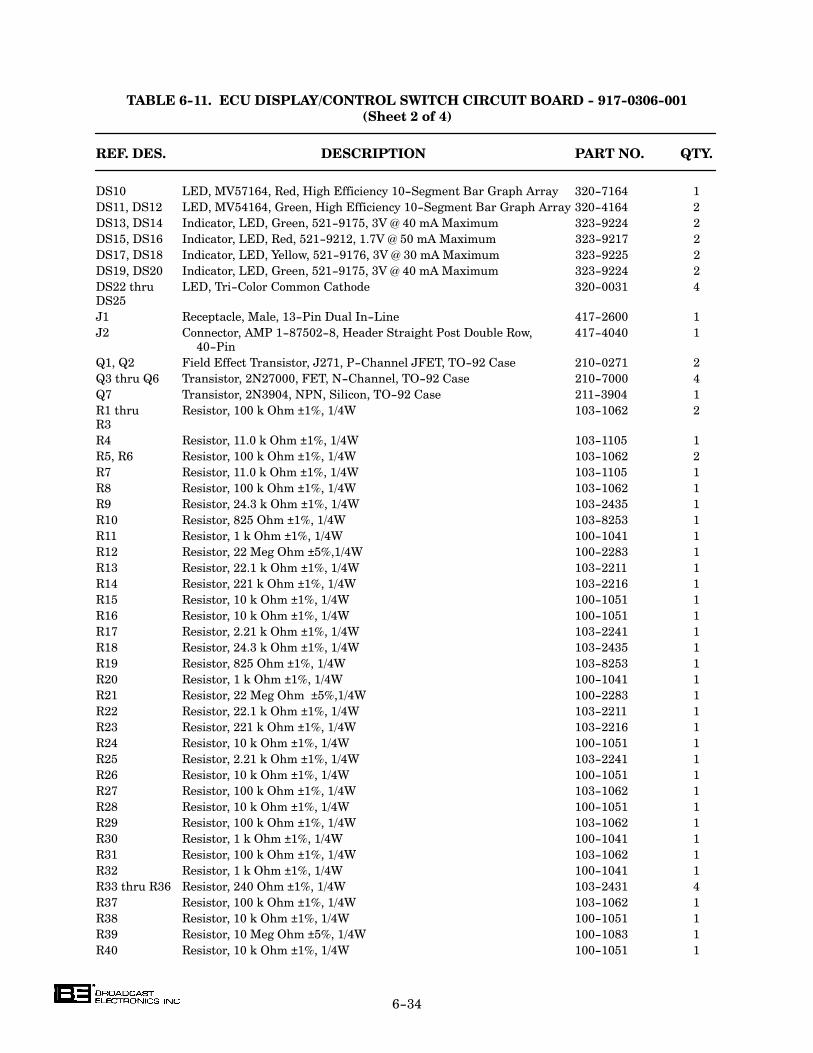
6-34
TABLE 6-11. ECU DISPLAY/CONTROL SWITCH CIRCUIT BOARD - 917-0306-001
(Sheet 2 of 4)
REF. DES. DESCRIPTION PART NO. QTY.
DS10 LED, MV57164, Red, High Efficiency 10-Segment Bar Graph Array 320-7164 1
DS11, DS12 LED, MV54164, Green, High Efficiency 10-Segment Bar Graph Array 320-4164 2
DS13, DS14 Indicator, LED, Green, 521-9175, 3V @ 40 mA Maximum 323-9224 2
DS15, DS16 Indicator, LED, Red, 521-9212, 1.7V @ 50 mA Maximum 323-9217 2
DS17, DS18 Indicator, LED, Yellow, 521-9176, 3V @ 30 mA Maximum 323-9225 2
DS19, DS20 Indicator, LED, Green, 521-9175, 3V @ 40 mA Maximum 323-9224 2
DS22 thru LED, Tri-Color Common Cathode 320-0031 4DS25
J1 Receptacle, Male, 13-Pin Dual In-Line 417-2600 1
J2 Connector, AMP 1-87502-8, Header Straight Post Double Row, 417-4040 140-Pin
Q1, Q2 Field Effect Transistor, J271, P-Channel JFET, TO-92 Case 210-0271 2
Q3 thru Q6 Transistor, 2N27000, FET, N-Channel, TO-92 Case 210-7000 4
Q7 Transistor, 2N3904, NPN, Silicon, TO-92 Case 211-3904 1
R1 thru Resistor, 100 k Ohm ±1%, 1/4W 103-1062 2R3
R4 Resistor, 11.0 k Ohm ±1%, 1/4W 103-1105 1
R5, R6 Resistor, 100 k Ohm ±1%, 1/4W 103-1062 2
R7 Resistor, 11.0 k Ohm ±1%, 1/4W 103-1105 1
R8 Resistor, 100 k Ohm ±1%, 1/4W 103-1062 1
R9 Resistor, 24.3 k Ohm ±1%, 1/4W 103-2435 1
R10 Resistor, 825 Ohm ±1%, 1/4W 103-8253 1
R11 Resistor, 1 k Ohm ±1%, 1/4W 100-1041 1
R12 Resistor, 22 Meg Ohm ±5%,1/4W 100-2283 1
R13 Resistor, 22.1 k Ohm ±1%, 1/4W 103-2211 1
R14 Resistor, 221 k Ohm ±1%, 1/4W 103-2216 1
R15 Resistor, 10 k Ohm ±1%, 1/4W 100-1051 1
R16 Resistor, 10 k Ohm ±1%, 1/4W 100-1051 1
R17 Resistor, 2.21 k Ohm ±1%, 1/4W 103-2241 1
R18 Resistor, 24.3 k Ohm ±1%, 1/4W 103-2435 1
R19 Resistor, 825 Ohm ±1%, 1/4W 103-8253 1
R20 Resistor, 1 k Ohm ±1%, 1/4W 100-1041 1
R21 Resistor, 22 Meg Ohm ±5%,1/4W 100-2283 1
R22 Resistor, 22.1 k Ohm ±1%, 1/4W 103-2211 1
R23 Resistor, 221 k Ohm ±1%, 1/4W 103-2216 1
R24 Resistor, 10 k Ohm ±1%, 1/4W 100-1051 1
R25 Resistor, 2.21 k Ohm ±1%, 1/4W 103-2241 1
R26 Resistor, 10 k Ohm ±1%, 1/4W 100-1051 1
R27 Resistor, 100 k Ohm ±1%, 1/4W 103-1062 1
R28 Resistor, 10 k Ohm ±1%, 1/4W 100-1051 1
R29 Resistor, 100 k Ohm ±1%, 1/4W 103-1062 1
R30 Resistor, 1 k Ohm ±1%, 1/4W 100-1041 1
R31 Resistor, 100 k Ohm ±1%, 1/4W 103-1062 1
R32 Resistor, 1 k Ohm ±1%, 1/4W 100-1041 1
R33 thru R36 Resistor, 240 Ohm ±1%, 1/4W 103-2431 4
R37 Resistor, 100 k Ohm ±1%, 1/4W 103-1062 1
R38 Resistor, 10 k Ohm ±1%, 1/4W 100-1051 1
R39 Resistor, 10 Meg Ohm ±5%, 1/4W 100-1083 1
R40 Resistor, 10 k Ohm ±1%, 1/4W 100-1051 1
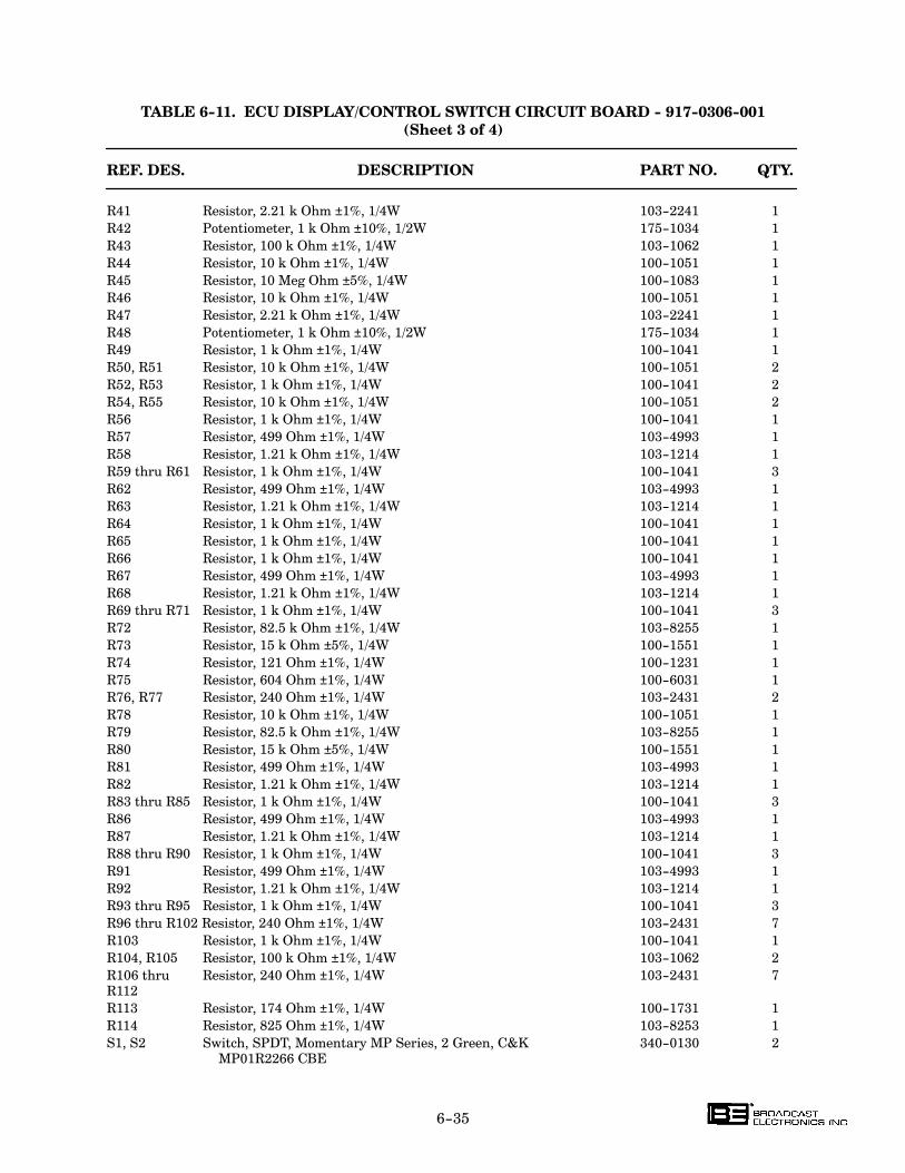
6-35
TABLE 6-11. ECU DISPLAY/CONTROL SWITCH CIRCUIT BOARD - 917-0306-001
(Sheet 3 of 4)
REF. DES. DESCRIPTION PART NO. QTY.
R41 Resistor, 2.21 k Ohm ±1%, 1/4W 103-2241 1
R42 Potentiometer, 1 k Ohm ±10%, 1/2W 175-1034 1
R43 Resistor, 100 k Ohm ±1%, 1/4W 103-1062 1
R44 Resistor, 10 k Ohm ±1%, 1/4W 100-1051 1
R45 Resistor, 10 Meg Ohm ±5%, 1/4W 100-1083 1
R46 Resistor, 10 k Ohm ±1%, 1/4W 100-1051 1
R47 Resistor, 2.21 k Ohm ±1%, 1/4W 103-2241 1
R48 Potentiometer, 1 k Ohm ±10%, 1/2W 175-1034 1
R49 Resistor, 1 k Ohm ±1%, 1/4W 100-1041 1
R50, R51 Resistor, 10 k Ohm ±1%, 1/4W 100-1051 2
R52, R53 Resistor, 1 k Ohm ±1%, 1/4W 100-1041 2
R54, R55 Resistor, 10 k Ohm ±1%, 1/4W 100-1051 2
R56 Resistor, 1 k Ohm ±1%, 1/4W 100-1041 1
R57 Resistor, 499 Ohm ±1%, 1/4W 103-4993 1
R58 Resistor, 1.21 k Ohm ±1%, 1/4W 103-1214 1
R59 thru R61 Resistor, 1 k Ohm ±1%, 1/4W 100-1041 3
R62 Resistor, 499 Ohm ±1%, 1/4W 103-4993 1
R63 Resistor, 1.21 k Ohm ±1%, 1/4W 103-1214 1
R64 Resistor, 1 k Ohm ±1%, 1/4W 100-1041 1
R65 Resistor, 1 k Ohm ±1%, 1/4W 100-1041 1
R66 Resistor, 1 k Ohm ±1%, 1/4W 100-1041 1
R67 Resistor, 499 Ohm ±1%, 1/4W 103-4993 1
R68 Resistor, 1.21 k Ohm ±1%, 1/4W 103-1214 1
R69 thru R71 Resistor, 1 k Ohm ±1%, 1/4W 100-1041 3
R72 Resistor, 82.5 k Ohm ±1%, 1/4W 103-8255 1
R73 Resistor, 15 k Ohm ±5%, 1/4W 100-1551 1
R74 Resistor, 121 Ohm ±1%, 1/4W 100-1231 1
R75 Resistor, 604 Ohm ±1%, 1/4W 100-6031 1
R76, R77 Resistor, 240 Ohm ±1%, 1/4W 103-2431 2
R78 Resistor, 10 k Ohm ±1%, 1/4W 100-1051 1
R79 Resistor, 82.5 k Ohm ±1%, 1/4W 103-8255 1
R80 Resistor, 15 k Ohm ±5%, 1/4W 100-1551 1
R81 Resistor, 499 Ohm ±1%, 1/4W 103-4993 1
R82 Resistor, 1.21 k Ohm ±1%, 1/4W 103-1214 1
R83 thru R85 Resistor, 1 k Ohm ±1%, 1/4W 100-1041 3
R86 Resistor, 499 Ohm ±1%, 1/4W 103-4993 1
R87 Resistor, 1.21 k Ohm ±1%, 1/4W 103-1214 1
R88 thru R90 Resistor, 1 k Ohm ±1%, 1/4W 100-1041 3
R91 Resistor, 499 Ohm ±1%, 1/4W 103-4993 1
R92 Resistor, 1.21 k Ohm ±1%, 1/4W 103-1214 1
R93 thru R95 Resistor, 1 k Ohm ±1%, 1/4W 100-1041 3
R96 thru R102 Resistor, 240 Ohm ±1%, 1/4W 103-2431 7
R103 Resistor, 1 k Ohm ±1%, 1/4W 100-1041 1
R104, R105 Resistor, 100 k Ohm ±1%, 1/4W 103-1062 2
R106 thru Resistor, 240 Ohm ±1%, 1/4W 103-2431 7R112
R113 Resistor, 174 Ohm ±1%, 1/4W 100-1731 1
R114 Resistor, 825 Ohm ±1%, 1/4W 103-8253 1
S1, S2 Switch, SPDT, Momentary MP Series, 2 Green, C&K 340-0130 2MP01R2266 CBE
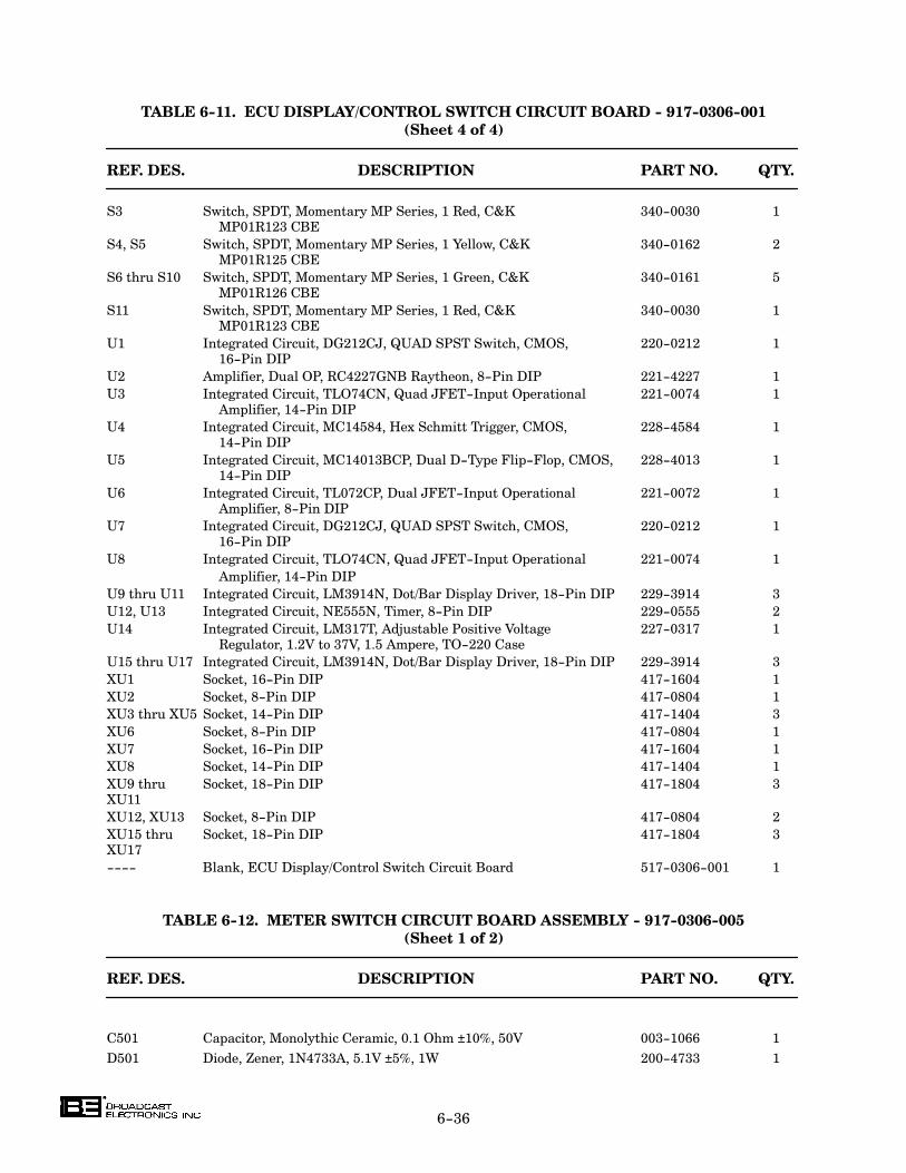
6-36
TABLE 6-11. ECU DISPLAY/CONTROL SWITCH CIRCUIT BOARD - 917-0306-001
(Sheet 4 of 4)
REF. DES. DESCRIPTION PART NO. QTY.
S3 Switch, SPDT, Momentary MP Series, 1 Red, C&K 340-0030 1MP01R123 CBE
S4, S5 Switch, SPDT, Momentary MP Series, 1 Yellow, C&K 340-0162 2MP01R125 CBE
S6 thru S10 Switch, SPDT, Momentary MP Series, 1 Green, C&K 340-0161 5MP01R126 CBE
S11 Switch, SPDT, Momentary MP Series, 1 Red, C&K 340-0030 1MP01R123 CBE
U1 Integrated Circuit, DG212CJ, QUAD SPST Switch, CMOS, 220-0212 116-Pin DIP
U2 Amplifier, Dual OP, RC4227GNB Raytheon, 8-Pin DIP 221-4227 1
U3 Integrated Circuit, TLO74CN, Quad JFET-Input Operational 221-0074 1Amplifier, 14-Pin DIP
U4 Integrated Circuit, MC14584, Hex Schmitt Trigger, CMOS, 228-4584 114-Pin DIP
U5 Integrated Circuit, MC14013BCP, Dual D-Type Flip-Flop, CMOS, 228-4013 114-Pin DIP
U6 Integrated Circuit, TL072CP, Dual JFET-Input Operational 221-0072 1Amplifier, 8-Pin DIP
U7 Integrated Circuit, DG212CJ, QUAD SPST Switch, CMOS, 220-0212 116-Pin DIP
U8 Integrated Circuit, TLO74CN, Quad JFET-Input Operational 221-0074 1
Amplifier, 14-Pin DIP
U9 thru U11 Integrated Circuit, LM3914N, Dot/Bar Display Driver, 18-Pin DIP 229-3914 3
U12, U13 Integrated Circuit, NE555N, Timer, 8-Pin DIP 229-0555 2
U14 Integrated Circuit, LM317T, Adjustable Positive Voltage 227-0317 1Regulator, 1.2V to 37V, 1.5 Ampere, TO-220 Case
U15 thru U17 Integrated Circuit, LM3914N, Dot/Bar Display Driver, 18-Pin DIP 229-3914 3
XU1 Socket, 16-Pin DIP 417-1604 1
XU2 Socket, 8-Pin DIP 417-0804 1
XU3 thru XU5 Socket, 14-Pin DIP 417-1404 3
XU6 Socket, 8-Pin DIP 417-0804 1
XU7 Socket, 16-Pin DIP 417-1604 1
XU8 Socket, 14-Pin DIP 417-1404 1
XU9 thru Socket, 18-Pin DIP 417-1804 3XU11
XU12, XU13 Socket, 8-Pin DIP 417-0804 2
XU15 thru Socket, 18-Pin DIP 417-1804 3XU17
---- Blank, ECU Display/Control Switch Circuit Board 517-0306-001 1
TABLE 6-12. METER SWITCH CIRCUIT BOARD ASSEMBLY - 917-0306-005
(Sheet 1 of 2)
REF. DES. DESCRIPTION PART NO. QTY.
C501 Capacitor, Monolythic Ceramic, 0.1 Ohm ±10%, 50V 003-1066 1
D501 Diode, Zener, 1N4733A, 5.1V ±5%, 1W 200-4733 1

6-37
TABLE 6-12. METER SWITCH CIRCUIT BOARD ASSEMBLY - 917-0306-005
(Sheet 2 of 2)
REF. DES. DESCRIPTION PART NO. QTY.
J501 Receptacle, 6-Pin 417-0677 1
J502 Socket, 4-Pin 418-0255 1
R501 Potentiometer, 500 Ohm, 1/2W 178-5030 1
R503 Potentiometer, 2 k Ohm ±10%, 1/2W 178-2044 1
R504 Resistor, 3.01 k Ohm ±1%, 1/4W 103-3014 1
R505 Potentiometer, 500 Ohm, 1/2W 178-5030 1
R506 Potentiometer, 2 k Ohm ±10%, 1/2W 178-2044 1
R507 Resistor, 3.01 k Ohm ±1%, 1/4W 103-3014 1
R508 Resistor, 2.74 k Ohm ±1%, 1/4W 103-2744 1
R509, R510 Resistor, 1.62 k Ohm ±1%, 1/4W 103-1624 2
R511 Potentiometer, 50 k Ohm ±10%, 1/2W 178-5054 1
S501, S502 Switch, Rotary, 3 Position 2 Pole 340-0134 2
---- Blank, Meter Switch Circuit Board 517-0306-005 1
TABLE 6-13. ECU WIRE HARNESS - 947-0153
REF. DES. DESCRIPTION PART NO. QTY.
P1 Housing, SL-156, 3 Position 417-0306 1
P1 Plug, Ribbon Cable, 26-Pin Dual In-line 418-2600 1
P2 Plug, 40-Pin, Dual In-line 417-0118 1
P2 Housing, SL-156, 6 Position 417-0606 1
P3 Plug, Ribbon Cable, 26-Pin Dual In-Line 418-2600 1
P7 Connector Housing, 6-Pin 418-0670 1
P8 Plug, 40-Pin, Dual In-line 417-0118 1
P10 Plug, Ribbon Cable, 26-Pin Dual In-line 418-2600 1
P502 Plug, Housing, 4-Pin 418-0240 1
P801 Plug, Ribbon Cable, 26-Pin Dual In-Line 418-2600 1
---- Pins, Connector 417-0053 10
TABLE 6-14. POWER MODULE ASSEMBLY - 957-0010-001
REF. DES. DESCRIPTION PART NO. QTY.
---- Modulator Circuit Board Assembly 917-0302 1
---- Power Amplifier Circuit Board Assembly 917-0304 2

6-38
TABLE 6-15. MODULATOR CIRCUIT BOARD ASSEMBLY- 917-0302
(Sheet 1 of 4)
REF. DES. DESCRIPTION PART NO. QTY.
C1 Capacitor, Electrolytic, 10 uF, 50V 023-1076 1
C2 Capacitor, Monolythic Ceramic, .1 uF ±10%, 100V 003-1041 1
C3 Capacitor, Electrolytic, 22 uF, 50V 024-2274 1
C4 Capacitor, Monolythic Ceramic 1 uF ±10%, 100V 003-1041 1
C5 Capacitor, Electrolytic, 330 uF, 200V dc 013-3385-001 1
C6 Capacitor, Polypropylene Film, .47 uF, 250V, Oval 033-4743 1
C7 Capacitor, Mica, 1000 pF ±10%, 350V 046-0002 1
C8 Capacitor, Electrolytic, 330 uF, 200V dc 013-3385-001 1
C9 Capacitor, Polypropylene Film, .47 uF, 250V, Oval 033-4743 1
C10 Capacitor, Mica, 1000 pF ±10%, 350V 046-0002 1
C11, C12 Capacitor, Monolythic Ceramic, .1 uF ±10%, 100V 003-1041 2
C13, C14 Capacitor, Polypropylene Film, 2.2 uF, 400V 030-2256 2
C15, C16 Capacitor, Metallized Polypropylene Film, .068 uF ±10%, 250V 030-6843 2
C17 Capacitor, Monolythic Ceramic, .1 uF ±10%, 100V 003-1041 1
C18, C19 Capacitor, Electrolytic, 10 uF, 50V 023-1076 2
C20 Capacitor, Monolythic Ceramic, .1 uF ±10%, 100V 003-1041 1
C21 Capacitor, Ceramic, 0.001 uF ±10%, 200V 030-1033 1
C22 Capacitor, Electrolytic, 10 uF, 50V 023-1076 1
C23 Capacitor, Electrolytic, 22 uF, 50V 024-2274 1
C24 Capacitor, Electrolytic, 10 uF, 50V 023-1076 1
C25 Capacitor, Electrolytic, 22 uF, 50V 024-2274 1
C26, C27 Capacitor, Monolythic Ceramic, .1 uF ±10%, 100V 003-1041 2
C28 thru C32 Capacitor, Electrolytic, 10 uF, 50V 023-1076 5
C33 Capacitor, Monolythic Ceramic, .1 uF ±10%, 100V 003-1041 1
C34 Capacitor, Electrolytic, 47 uF, 35V 020-4773 1
C35 Capacitor, Electrolytic, 10 uF, 50V 023-1076 1
C36, C37 Capacitor, Ceramic, 0.001 uF ±10%, 200V 030-1033 2
C38, C39 Capacitor, Monolythic Ceramic, .1 uF ±10%, 100V 003-1041 2
C40 Capacitor, Electrolytic, 10 uF, 50V 023-1076 1
C41 Capacitor, Electrolytic, 33 uF, 25V 020-3374 1
C42 Capacitor, Polypropylene Film, 2.2 uF, 400V 030-2256 1
C43 Capacitor, Polypropylene Film, .47 uF, 250V, Oval 033-4743 1
C44 Capacitor, Polypropylene Film, .033 uF, ±10%, 200V 030-3353 1
C45 Capacitor, Mica, 820 pF ±5%, 300V 042-8222 1
C46, C47 Capacitor, Monolythic Ceramic, .1 uF ±10%, 100V 003-1041 2
C48 Capacitor, Metallized Polypropylene Film, .068 uF ±10%, 250V 030-6843 1
C49 Capacitor, Polypropylene Film, .033 uF ±10%, 200V 030-3353 1
C50 Capacitor, Mylar, 0.01 uF ±10%, 100V 031-1043 1
D1 Diode, Zener, 1N4733A, 5.1V ±5%, 1W 200-4733 1
D2, D3 Diode, Fast Recovery, 16JPF20 200-1620 2
D4 Diode, 1N4005, Silicon, 600V @ 1 Ampere 203-4005 1
D5 Diode, 1N4148, Silicon, 75V @ 0.3 Amperes 203-4148 1
D6 Diode, 1N4005, Silicon, 600V @ 1 Ampere 203-4005 1
D7 Diode, Zener, 1N4739A, 9.1V ±5%, 1W 200-0009 1
D8, D9 Diode, 1N4005, Silicon, 600V @ 1 Ampere 203-4005 2
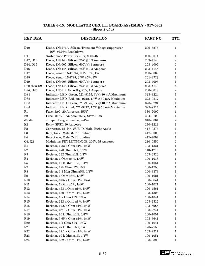
6-39
TABLE 6-15. MODULATOR CIRCUIT BOARD ASSEMBLY - 917-0302
(Sheet 2 of 4)
REF. DES. DESCRIPTION PART NO. QTY.
D10 Diode, 1N6276A, Silicon, Transient Voltage Suppressor, 206-6276 1
16V ±0.05% Breakdown
D11 Switchmode Power Rectifier, MUR460 230-0014 1
D12, D13 Diode, 1N4148, Silicon, 75V @ 0.3 Amperes 203-4148 2
D14, D15 Diode, 1N4005, Silicon, 600V @ 1 Ampere 203-4005 2
D16 Diode, 1N4148, Silicon, 75V @ 0.3 Amperes 203-4148 1
D17 Diode, Zener, 1N4739A, 9.1V ±5%, 1W 200-0009 1
D18 Diode, Zener, 1N4728, 3.3V ±5%, 1W 201-4728 1
D19 Diode, 1N4005, Silicon, 600V @ 1 Ampere 203-4005 1
D20 thru D23 Diode, 1N4148, Silicon, 75V @ 0.3 Amperes 203-4148 4
D24, D25 Diode, 1N5817, Schottky, 20V, 1 Ampere 200-0019 2
DS1 Indicator, LED, Green, 521-9175, 3V @ 40 mA Maximum 323-9224 1
DS2 Indicator, LED, Red, 521-9212, 1.7V @ 50 mA Maximum 323-9217 1
DS3 Indicator, LED, Green, 521-9175, 3V @ 40 mA Maximum 323-9224 1
DS4 Indicator, LED, Red, 521-9212, 1.7V @ 50 mA Maximum 323-9217 1
F1 Fuse, 3AG, 20 Amperes, 250V 330-2000 1
F2 Fuse, MDL, 1 Ampere, 250V, Slow-Blow 334-0100 1
J3, J4 Jumper, Programmable, 2-Pin 340-0004 2
K1 Relay, SPST, 30 Amperes 270-1213 1
P2 Connector, 15-Pin, SUB-D, Male, Right Angle 417-0374 1
P3 Receptacle, Male, 3-Pin In-line 417-0003 1
P4 Receptacle, Male, 2-Pin In-line 417-4004 1
Q1, Q2 Modulator, FET MTY55N20E, 200V, 55 Amperes 210-0550 2
R1 Resistor, 1.33 k Ohm ±1%, 1/4W 103-1331 1
R2 Resistor, 470 Ohm ±5%, 1/2W 110-4733 1
R3 Resistor, 332 Ohm ±1%, 1/4W 103-3323 1
R4 Resistor, 1 Ohm ±5%, 1/4W 100-1013 1
R5 Resistor, 10 k Ohm ±1%, 1/4W 100-1051 1
R7 Resistor, 12k Ohm, 2W, ±5% 130-1253 1
R8 Resistor, 3.3 Meg Ohm ±5%, 1/4W 100-3373 1
R9 Resistor, 1 Ohm ±5%, 1/4W 100-1021 1
R10 Resistor, 3.65 k Ohm ±1%, 1/4W 103-3641 1
R11 Resistor, 1 Ohm ±5%, 1/4W 100-1021 1
R12 Resistor, 453 k Ohm ±1%, 1/4W 100-4561 1
R13 Resistor, 130 k Ohm ±1%, 1/4W 103-1306 1
R14 Resistor, 1 k Ohm ±1%, 1/4W 100-1041 1
R15 Resistor, 332 k Ohm ±1%, 1/4W 103-3326 1
R16 Resistor, 69.8 k Ohm ±1%, 1/4W 103-6985 1
R17 Resistor, 2.21 k Ohm ±1%, 1/4W 103-2241 1
R18 Resistor, 10 k Ohm ±1%, 1/4W 100-1051 1
R19 Resistor, 3.65 k Ohm ±1%, 1/4W 103-3641 1
R20 Resistor, 1 k Ohm ±1%, 1/4W 100-1041 1
R21 Resistor, 27 k Ohm ±5%, 1W 120-2753 1
R22 Resistor, 22.1 k Ohm ±1%, 1/4W 103-2211 1
R23 Resistor, 10 k Ohm ±1%, 1/4W 100-1051 1
R24 Resistor, 332 k Ohm ±1%, 1/4W 103-3326 1
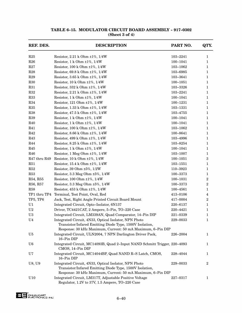
6-40
TABLE 6-15. MODULATOR CIRCUIT BOARD ASSEMBLY - 917-0302
(Sheet 3 of 4)
REF. DES. DESCRIPTION PART NO. QTY.
R25 Resistor, 2.21 k Ohm ±1%, 1/4W 103-2241 1
R26 Resistor, 1 k Ohm ±1%, 1/4W 100-1041 1
R27 Resistor, 100 k Ohm ±1%, 1/4W 103-1062 1
R28 Resistor, 69.8 k Ohm ±1%, 1/4W 103-6985 1
R29 Resistor, 3.65 k Ohm ±1%, 1/4W 103-3641 1
R30 Resistor, 10 k Ohm ±1%, 1/4W 100-1051 1
R31 Resistor, 332 k Ohm ±1%, 1/4W 103-3326 1
R32 Resistor, 2.21 k Ohm ±1%, 1/4W 103-2241 1
R33 Resistor, 1 k Ohm ±1%, 1/4W 100-1041 1
R34 Resistor, 121 Ohm ±1%, 1/4W 100-1231 1
R35 Resistor, 1.33 k Ohm ±1%, 1/4W 103-1331 1
R38 Resistor, 47.5 k Ohm ±1%, 1/4W 103-4755 1
R39 Resistor, 1 k Ohm ±1%, 1/4W 100-1041 1
R40 Resistor, 1 k Ohm ±1%, 1/4W 100-1041 1
R41 Resistor, 100 k Ohm ±1%, 1/4W 103-1062 1
R42 Resistor, 8.66 k Ohm ±1%, 1/4W 100-8641 1
R43 Resistor, 499 k Ohm ±1%, 1/4W 103-4996 1
R44 Resistor, 8.25 k Ohm ±1%, 1/4W 103-8254 1
R45 Resistor, 1 k Ohm ±1%, 1/4W 100-1041 1
R46 Resistor, 1 Meg Ohm ±1%, 1/4W 103-1007 1
R47 thru R49 Resistor, 10 k Ohm ±1%, 1/4W 100-1051 3
R51 Resistor, 15.4 k Ohm ±1%, 1/4W 103-1551 1
R52 Resistor, 39 Ohm ±5%, 1/2W 110-3923 1
R53 Resistor, 3.3 Meg Ohm ±5%, 1/4W 100-3373 1
R54, R55 Resistor, 100 Ohm ±1%, 1/4W 100-1031 2
R56, R57 Resistor, 3.3 Meg Ohm ±5%, 1/4W 100-3373 2
R58 Resistor, 453 k Ohm ±1%, 1/4W 100-4561 1
TP1 thru TP4 Terminal, Test Point, Oval, Red 413-0106 4
TP5, TP6 Jack, Test, Right Angle Printed Circuit Board Mount 417-0004 2
U1 Integrated Circuit, Opto-Isolator, 6N137 220-6137 1
U2 Driver, TC4421CAT, 2 Ampere, 5-Pin, TO-220 Case 220-4421 1
U3 Integrated Circuit, LM339AN, Quad Comparator, 14-Pin DIP 221-0339 1
U4 Integrated Circuit, 4N33, Optical Isolator, NPN Photo 229-0033 1
Transistor/Infared Emitting Diode Type, 1500V Isolation,
Response: 30 kHz Maximum, Current: 50 mA Maximum, 6-Pin DIP
U5 Integrated Circuit, ULN2004, 7 NPN Darlington Driver Pack, 226-2004 1
16-Pin DIP
U6 Integrated Circuit, MC14093B, Quad 2-Input NAND Schmitt Trigger, 220-4093 1
CMOS, 14-Pin DIP
U7 Integrated Circuit, MC14044BP, Quad NAND R-S Latch, CMOS, 228-4044 1
16-Pin DIP
U8, U9 Integrated Circuit, 4N33, Optical Isolator, NPN Photo 229-0033 2
Transistor/Infared Emitting Diode Type, 1500V Isolation,
Response: 30 kHz Maximum, Current: 50 mA Maximum, 6-Pin DIP
U10 Integrated Circuit, LM317T, Adjustable Positive Voltage 227-0317 1
Regulator, 1.2V to 37V, 1.5 Ampere, TO-220 Case
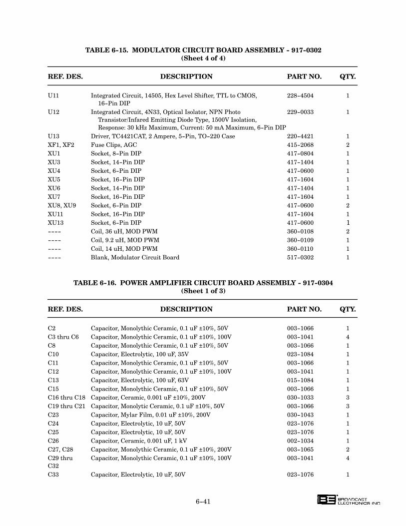
6-41
TABLE 6-15. MODULATOR CIRCUIT BOARD ASSEMBLY - 917-0302
(Sheet 4 of 4)
REF. DES. DESCRIPTION PART NO. QTY.
U11 Integrated Circuit, 14505, Hex Level Shifter, TTL to CMOS, 228-4504 1
16-Pin DIP
U12 Integrated Circuit, 4N33, Optical Isolator, NPN Photo 229-0033 1
Transistor/Infared Emitting Diode Type, 1500V Isolation,
Response: 30 kHz Maximum, Current: 50 mA Maximum, 6-Pin DIP
U13 Driver, TC4421CAT, 2 Ampere, 5-Pin, TO-220 Case 220-4421 1
XF1, XF2 Fuse Clips, AGC 415-2068 2
XU1 Socket, 8-Pin DIP 417-0804 1
XU3 Socket, 14-Pin DIP 417-1404 1
XU4 Socket, 6-Pin DIP 417-0600 1
XU5 Socket, 16-Pin DIP 417-1604 1
XU6 Socket, 14-Pin DIP 417-1404 1
XU7 Socket, 16-Pin DIP 417-1604 1
XU8, XU9 Socket, 6-Pin DIP 417-0600 2
XU11 Socket, 16-Pin DIP 417-1604 1
XU13 Socket, 6-Pin DIP 417-0600 1
---- Coil, 36 uH, MOD PWM 360-0108 2
---- Coil, 9.2 uH, MOD PWM 360-0109 1
---- Coil, 14 uH, MOD PWM 360-0110 1
---- Blank, Modulator Circuit Board 517-0302 1
TABLE 6-16. POWER AMPLIFIER CIRCUIT BOARD ASSEMBLY - 917-0304
(Sheet 1 of 3)
REF. DES. DESCRIPTION PART NO. QTY.
C2 Capacitor, Monolythic Ceramic, 0.1 uF ±10%, 50V 003-1066 1
C3 thru C6 Capacitor, Monolythic Ceramic, 0.1 uF ±10%, 100V 003-1041 4
C8 Capacitor, Monolythic Ceramic, 0.1 uF ±10%, 50V 003-1066 1
C10 Capacitor, Electrolytic, 100 uF, 35V 023-1084 1
C11 Capacitor, Monolythic Ceramic, 0.1 uF ±10%, 50V 003-1066 1
C12 Capacitor, Monolythic Ceramic, 0.1 uF ±10%, 100V 003-1041 1
C13 Capacitor, Electrolytic, 100 uF, 63V 015-1084 1
C15 Capacitor, Monolythic Ceramic, 0.1 uF ±10%, 50V 003-1066 1
C16 thru C18 Capacitor, Ceramic, 0.001 uF ±10%, 200V 030-1033 3
C19 thru C21 Capacitor, Monolytic Ceramic, 0.1 uF ±10%, 50V 003-1066 3
C23 Capacitor, Mylar Film, 0.01 uF ±10%, 200V 030-1043 1
C24 Capacitor, Electrolytic, 10 uF, 50V 023-1076 1
C25 Capacitor, Electrolytic, 10 uF, 50V 023-1076 1
C26 Capacitor, Ceramic, 0.001 uF, 1 kV 002-1034 1
C27, C28 Capacitor, Monolythic Ceramic, 0.1 uF ±10%, 200V 003-1065 2
C29 thru Capacitor, Monolythic Ceramic, 0.1 uF ±10%, 100V 003-1041 4
C32
C33 Capacitor, Electrolytic, 10 uF, 50V 023-1076 1
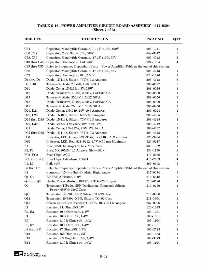
6-42
TABLE 6-16. POWER AMPLIFIER CIRCUIT BOARD ASSEMBLY - 917-0304
(Sheet 2 of 3)
REF. DES. DESCRIPTION PART NO. QTY.
C34 Capacitor, Monolythic Ceramic, 0.1 uF ±10%, 100V 003-1041 1
C36 ,C37 Capacitor, Mica, 39 pF ±5%, 500V 042-3912 2
C38, C39 Capacitor, Monolythic Ceramic, .47 uF ±10%, 50V 003-4743 2
C40 thru C43 Capacitor, Electrolytic, 1 uF, 50V 024-1064 4
C45 thru C55 Refer to Frequency Dependant Parts - Power Amplifier Table at the end of this section.
C58 Capacitor, Monolythic Ceramic, .47 uF ±10%, 50V 003-4743 1
C59 Capacitor, Electrolytic, 10 uF, 50V 023-1076 1
D1 thru D6 Diode, 1N4148, Silicon, 75V @ 0.3 Amperes 203-4148 6
D9, D10 Transzorb Diode, 27 Volt, 1.5KE27CA 206-0027 2
D11 Diode, Zener 1N5229, 4.3V, 0.5W 201-0035 1
D16 Diode, Transzorb, Diode, 300BV, 1.5FE300CA 206-0300 1
D17 Transzorb Diode, 250BV, 1.5KE250CA 206-0250 1
D18 Diode, Transzorb, Diode, 300BV, 1.5FE300CA 206-0300 1
D19 Transzorb Diode, 250BV, 1.5KE250CA 206-0250 1
D20, D21 Diode, Zener, 1N4749, 24V, 10.5 Amperes 200-0024 2
D22, D23 Diode, 1N4005, Silicon, 600V @ 1 Ampere 203-4005 2
D25 thru D28 Diode, 1N4148, Silicon, 75V @ 0.3 Amperes 203-4148 4
D29, D30 Diode, Zener, 1N4742A, 12V ±5%, 1W 200-4742 2
D31 Diode, Zener, 1N4737A, 7.5V, 1W, 34 mA 200-4737 1
D32 thru D35 Diode, 1N4148, Silicon, 75V @ 0.3 Amperes 203-4148 4
DS1 Indicator, LED, Green, 521-9175, 3V @ 40 mA Maximum 323-9224 1
DS2 Indicator, LED, Red, 521-9212, 1.7V @ 50 mA Maximum 323-9217 1
F1 Fuse, 3AB, 15 Amperes, 65V, Very Fast 330-1502 1
F2, F3 Fuse, 5 X 20MM, 1.5 Ampere, Slow-Blow 334-1150 2
FC1, FC2 Fuse Clips, AGC 415-2068 2
FC3 thru FC6 Fuse Clips, Littlefuse, 111501 415-2069 4
L1, L2 Coil, 4uH 360-0112 2
L3 thru L7 Refer to Frequency Dependant Parts - Power Amplifier Table at the end of this section.
P2 Connector, 15-Pin Sub-D, Male, Right Angle 417-0374 1
Q1, Q2 RF FET, APT6018, 600V 210-6018 2
Q3 thru Q6 Hexfet Power Mosfet, IRFI520G, TO-220 Fullpak 210-0520 4
Q7 Transistor, TIP120, NPN Darlington-Connected Silicon 210-0120 1
Power, 65W @ 25#C Case
Q11 Transistor, 2N3906, PNP, Silicon, TO-92 Case 210-3906 1
Q12 Transistor, 2N3904, NPN, Silicon, TO-92 Case 211-3904 1
Q13 Silicon Controlled Rectifier, GE6CA, 100V @ 1.6 Ampere 237-0006 1
R1 Resistor, 1 k Ohm ±5%,1W 120-1043 1
R2, R3 Resistor, 10 k Ohm ±1%, 1/4W 100-1051 2
R4 Resistor, 100 Ohm ±1%, 1/4W 100-1031 1
R5 Resistor, 1.10 k Ohm ±1%, 1/4W 103-1104 1
R6, R7 Resistor, 10 k Ohm ±1%, 1/4W 100-1051 2
R8 thru R11 Resistor, 27 Ohm ±5%, 1/4W 100-2723 4
R12 Resistor, 15k Ohm ±5%, 2W 130-1553 1
R13 Resistor, 3.3 Meg Ohm ±5%, 1/4W 100-3373 1
R14 Resistor, 1.10 k Ohm ±1%, 1/4W 103-1104 1
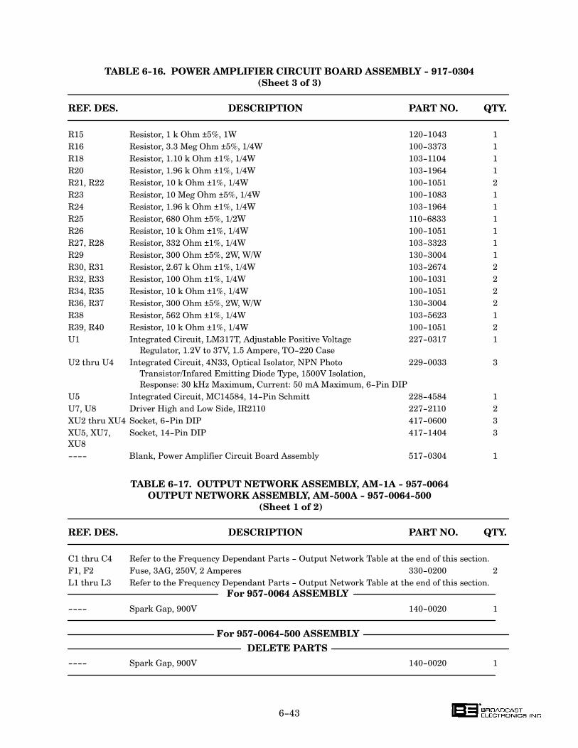
6-43
TABLE 6-16. POWER AMPLIFIER CIRCUIT BOARD ASSEMBLY - 917-0304
(Sheet 3 of 3)
REF. DES. DESCRIPTION PART NO. QTY.
R15 Resistor, 1 k Ohm ±5%, 1W 120-1043 1
R16 Resistor, 3.3 Meg Ohm ±5%, 1/4W 100-3373 1
R18 Resistor, 1.10 k Ohm ±1%, 1/4W 103-1104 1
R20 Resistor, 1.96 k Ohm ±1%, 1/4W 103-1964 1
R21, R22 Resistor, 10 k Ohm ±1%, 1/4W 100-1051 2
R23 Resistor, 10 Meg Ohm ±5%, 1/4W 100-1083 1
R24 Resistor, 1.96 k Ohm ±1%, 1/4W 103-1964 1
R25 Resistor, 680 Ohm ±5%, 1/2W 110-6833 1
R26 Resistor, 10 k Ohm ±1%, 1/4W 100-1051 1
R27, R28 Resistor, 332 Ohm ±1%, 1/4W 103-3323 1
R29 Resistor, 300 Ohm ±5%, 2W, W/W 130-3004 1
R30, R31 Resistor, 2.67 k Ohm ±1%, 1/4W 103-2674 2
R32, R33 Resistor, 100 Ohm ±1%, 1/4W 100-1031 2
R34, R35 Resistor, 10 k Ohm ±1%, 1/4W 100-1051 2
R36, R37 Resistor, 300 Ohm ±5%, 2W, W/W 130-3004 2
R38 Resistor, 562 Ohm ±1%, 1/4W 103-5623 1
R39, R40 Resistor, 10 k Ohm ±1%, 1/4W 100-1051 2
U1 Integrated Circuit, LM317T, Adjustable Positive Voltage 227-0317 1
Regulator, 1.2V to 37V, 1.5 Ampere, TO-220 Case
U2 thru U4 Integrated Circuit, 4N33, Optical Isolator, NPN Photo 229-0033 3
Transistor/Infared Emitting Diode Type, 1500V Isolation,
Response: 30 kHz Maximum, Current: 50 mA Maximum, 6-Pin DIP
U5 Integrated Circuit, MC14584, 14-Pin Schmitt 228-4584 1
U7, U8 Driver High and Low Side, IR2110 227-2110 2
XU2 thru XU4 Socket, 6-Pin DIP 417-0600 3
XU5, XU7, Socket, 14-Pin DIP 417-1404 3
XU8
---- Blank, Power Amplifier Circuit Board Assembly 517-0304 1
TABLE 6-17. OUTPUT NETWORK ASSEMBLY, AM-1A - 957-0064
OUTPUT NETWORK ASSEMBLY, AM-500A - 957-0064-500
(Sheet 1 of 2)
REF. DES. DESCRIPTION PART NO. QTY.
C1 thru C4 Refer to the Frequency Dependant Parts - Output Network Table at the end of this section.
F1, F2 Fuse, 3AG, 250V, 2 Amperes 330-0200 2
L1 thru L3 Refer to the Frequency Dependant Parts - Output Network Table at the end of this section.
For 957-0064 ASSEMBLY
---- Spark Gap, 900V 140-0020 1
For 957-0064-500 ASSEMBLY
DELETE PARTS
---- Spark Gap, 900V 140-0020 1

6-44
TABLE 6-17. OUTPUT NETWORK ASSEMBLY, AM-1A - 957-0064
OUTPUT NETWORK ASSEMBLY, AM-500A - 957-0064-500
(Sheet 2 of 2)
REF. DES. DESCRIPTION PART NO. QTY.
For 957-0064-500 ASSEMBLY
ADD PARTS
---- Spark Gap, 650V 140-0034 1
---- Circuit Breaker, 15 Amperes, 2-Pole, 250V ac 341-0032 1
---- Choke, 3.6 mH, AM Transmitter 370-2363 1
---- Metal-Oxide Varistor, B40K275, 275V, 1680 Joules 140-0021 3
---- RFI Filter, 30VB6 339-0024 1
---- Circuit Breaker, 20 Amperes, 2-Pole, 250V ac 341-0063 1
---- Choke, 1.04 mH, AM Transmitter 370-2364 1
---- Transformer, AM Transmitter Power Supply 376-0047 1
---- Fan, 7 inch (17.78 cm) 114/235 ft3/min 110/220V ac, 50/60 Hz 380-9001 1
---- Air Filter, FXA 7.50"x7.50" x .86" 407-0173 1
---- Barrier Strip, 9 Terminal 412-0090 1
---- Fuse Holder, AGC 415-2012 2
---- Pin Connector 417-0036 2
---- Pins, Connector 417-0053 10
---- Receptacle, BNC 417-0203 1
---- Receptacle, Type N 417-0204 1
---- Connector, 2 Pole 3 Wire, 15A, 250V 418-0320 1
---- Connector Housing, 2-Pin, Male 418-0702 1
---- Plug, Connector Housing, 12-Pin 418-1271 1
---- Power Block Motherboard Circuit Board Assembly 917-0303-001 1
---- Directional Coupler Circuit Board Assembly 917-0306-002 1
---- AC Sample Circuit Board Assembly 917-0306-007 1
---- Temperature Sensor Circuit Board Assembly 917-0306-009 1
---- Lightning Detection Circuit Board Assembly 917-0306-014 1
---- Power Supply Circuit Board Assembly 917-0315-001 1
---- Power Supply Bulk Capacitor Circuit Board Assembly 917-0315-003 1
---- Power Supply Capacitor Circuit Board Assembly 917-0315-005 1
---- Wiring Harness, Fan Assembly 947-0209 1
For 957-0064 ASSEMBLY
---- Lightning Protection Circuit Board Assembly 917-0316 1
For 957-0064-500 ASSEMBLY
---- Lightning Protection Circuit Board Assembly 917-0216 1
---- Combiner Circuit Board Assembly 917-0321-001 1
---- Optically Coupled Relay Circuit Board Assembly 919-0096-001 1
---- Wire Harness 947-0179 1
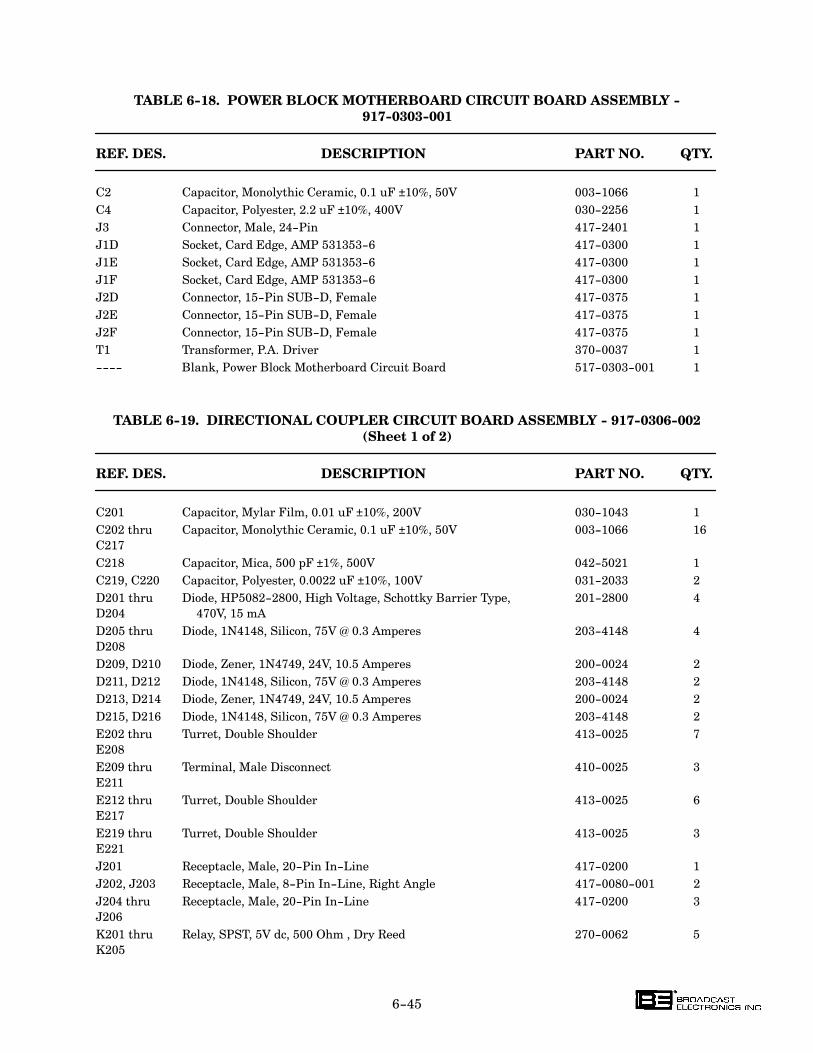
6-45
TABLE 6-18. POWER BLOCK MOTHERBOARD CIRCUIT BOARD ASSEMBLY -
917-0303-001
REF. DES. DESCRIPTION PART NO. QTY.
C2 Capacitor, Monolythic Ceramic, 0.1 uF ±10%, 50V 003-1066 1
C4 Capacitor, Polyester, 2.2 uF ±10%, 400V 030-2256 1
J3 Connector, Male, 24-Pin 417-2401 1
J1D Socket, Card Edge, AMP 531353-6 417-0300 1
J1E Socket, Card Edge, AMP 531353-6 417-0300 1
J1F Socket, Card Edge, AMP 531353-6 417-0300 1
J2D Connector, 15-Pin SUB-D, Female 417-0375 1
J2E Connector, 15-Pin SUB-D, Female 417-0375 1
J2F Connector, 15-Pin SUB-D, Female 417-0375 1
T1 Transformer, P.A. Driver 370-0037 1
---- Blank, Power Block Motherboard Circuit Board 517-0303-001 1
TABLE 6-19. DIRECTIONAL COUPLER CIRCUIT BOARD ASSEMBLY - 917-0306-002
(Sheet 1 of 2)
REF. DES. DESCRIPTION PART NO. QTY.
C201 Capacitor, Mylar Film, 0.01 uF ±10%, 200V 030-1043 1
C202 thru Capacitor, Monolythic Ceramic, 0.1 uF ±10%, 50V 003-1066 16
C217
C218 Capacitor, Mica, 500 pF ±1%, 500V 042-5021 1
C219, C220 Capacitor, Polyester, 0.0022 uF ±10%, 100V 031-2033 2
D201 thru Diode, HP5082-2800, High Voltage, Schottky Barrier Type, 201-2800 4
D204 470V, 15 mA
D205 thru Diode, 1N4148, Silicon, 75V @ 0.3 Amperes 203-4148 4
D208
D209, D210 Diode, Zener, 1N4749, 24V, 10.5 Amperes 200-0024 2
D211, D212 Diode, 1N4148, Silicon, 75V @ 0.3 Amperes 203-4148 2
D213, D214 Diode, Zener, 1N4749, 24V, 10.5 Amperes 200-0024 2
D215, D216 Diode, 1N4148, Silicon, 75V @ 0.3 Amperes 203-4148 2
E202 thru Turret, Double Shoulder 413-0025 7
E208
E209 thru Terminal, Male Disconnect 410-0025 3
E211
E212 thru Turret, Double Shoulder 413-0025 6
E217
E219 thru Turret, Double Shoulder 413-0025 3
E221
J201 Receptacle, Male, 20-Pin In-Line 417-0200 1
J202, J203 Receptacle, Male, 8-Pin In-Line, Right Angle 417-0080-001 2
J204 thru Receptacle, Male, 20-Pin In-Line 417-0200 3
J206
K201 thru Relay, SPST, 5V dc, 500 Ohm , Dry Reed 270-0062 5
K205
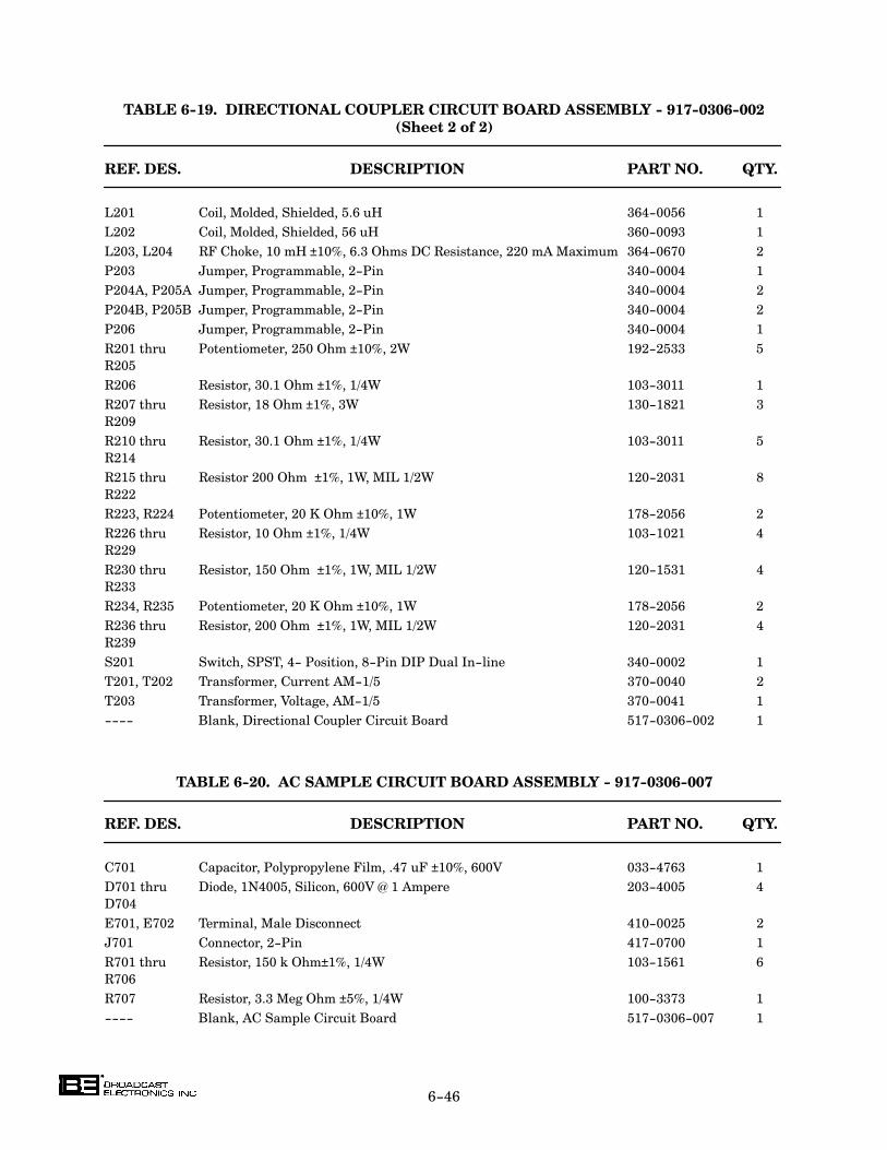
6-46
TABLE 6-19. DIRECTIONAL COUPLER CIRCUIT BOARD ASSEMBLY - 917-0306-002
(Sheet 2 of 2)
REF. DES. DESCRIPTION PART NO. QTY.
L201 Coil, Molded, Shielded, 5.6 uH 364-0056 1
L202 Coil, Molded, Shielded, 56 uH 360-0093 1
L203, L204 RF Choke, 10 mH ±10%, 6.3 Ohms DC Resistance, 220 mA Maximum 364-0670 2
P203 Jumper, Programmable, 2-Pin 340-0004 1
P204A, P205A Jumper, Programmable, 2-Pin 340-0004 2
P204B, P205B Jumper, Programmable, 2-Pin 340-0004 2
P206 Jumper, Programmable, 2-Pin 340-0004 1
R201 thru Potentiometer, 250 Ohm ±10%, 2W 192-2533 5
R205
R206 Resistor, 30.1 Ohm ±1%, 1/4W 103-3011 1
R207 thru Resistor, 18 Ohm ±1%, 3W 130-1821 3
R209
R210 thru Resistor, 30.1 Ohm ±1%, 1/4W 103-3011 5
R214
R215 thru Resistor 200 Ohm ±1%, 1W, MIL 1/2W 120-2031 8
R222
R223, R224 Potentiometer, 20 K Ohm ±10%, 1W 178-2056 2
R226 thru Resistor, 10 Ohm ±1%, 1/4W 103-1021 4
R229
R230 thru Resistor, 150 Ohm ±1%, 1W, MIL 1/2W 120-1531 4
R233
R234, R235 Potentiometer, 20 K Ohm ±10%, 1W 178-2056 2
R236 thru Resistor, 200 Ohm ±1%, 1W, MIL 1/2W 120-2031 4
R239
S201 Switch, SPST, 4- Position, 8-Pin DIP Dual In-line 340-0002 1
T201, T202 Transformer, Current AM-1/5 370-0040 2
T203 Transformer, Voltage, AM-1/5 370-0041 1
---- Blank, Directional Coupler Circuit Board 517-0306-002 1
TABLE 6-20. AC SAMPLE CIRCUIT BOARD ASSEMBLY - 917-0306-007
REF. DES. DESCRIPTION PART NO. QTY.
C701 Capacitor, Polypropylene Film, .47 uF ±10%, 600V 033-4763 1
D701 thru Diode, 1N4005, Silicon, 600V @ 1 Ampere 203-4005 4
D704
E701, E702 Terminal, Male Disconnect 410-0025 2
J701 Connector, 2-Pin 417-0700 1
R701 thru Resistor, 150 k Ohm±1%, 1/4W 103-1561 6
R706
R707 Resistor, 3.3 Meg Ohm ±5%, 1/4W 100-3373 1
---- Blank, AC Sample Circuit Board 517-0306-007 1
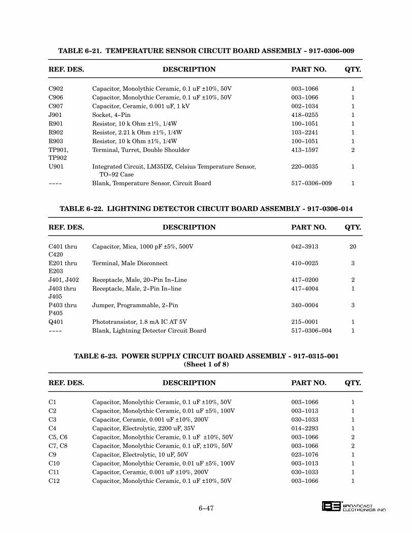
6-47
TABLE 6-21. TEMPERATURE SENSOR CIRCUIT BOARD ASSEMBLY - 917-0306-009
REF. DES. DESCRIPTION PART NO. QTY.
C902 Capacitor, Monolythic Ceramic, 0.1 uF ±10%, 50V 003-1066 1
C906 Capacitor, Monolythic Ceramic, 0.1 uF ±10%, 50V 003-1066 1
C907 Capacitor, Ceramic, 0.001 uF, 1 kV 002-1034 1
J901 Socket, 4-Pin 418-0255 1
R901 Resistor, 10 k Ohm ±1%, 1/4W 100-1051 1
R902 Resistor, 2.21 k Ohm ±1%, 1/4W 103-2241 1
R903 Resistor, 10 k Ohm ±1%, 1/4W 100-1051 1
TP901, Terminal, Turret, Double Shoulder 413-1597 2
TP902
U901 Integrated Circuit, LM35DZ, Celsius Temperature Sensor, 220-0035 1
TO-92 Case
---- Blank, Temperature Sensor, Circuit Board 517-0306-009 1
TABLE 6-22. LIGHTNING DETECTOR CIRCUIT BOARD ASSEMBLY - 917-0306-014
REF. DES. DESCRIPTION PART NO. QTY.
C401 thru Capacitor, Mica, 1000 pF ±5%, 500V 042-3913 20
C420
E201 thru Terminal, Male Disconnect 410-0025 3
E203
J401, J402 Receptacle, Male, 20-Pin In-Line 417-0200 2
J403 thru Receptacle, Male, 2-Pin In-line 417-4004 1
J405
P403 thru Jumper, Programmable, 2-Pin 340-0004 3
P405
Q401 Phototransistor, 1.8 mA IC AT 5V 215-0001 1
---- Blank, Lightning Detector Circuit Board 517-0306-004 1
TABLE 6-23. POWER SUPPLY CIRCUIT BOARD ASSEMBLY - 917-0315-001
(Sheet 1 of 8)
REF. DES. DESCRIPTION PART NO. QTY.
C1 Capacitor, Monolythic Ceramic, 0.1 uF ±10%, 50V 003-1066 1
C2 Capacitor, Monolythic Ceramic, 0.01 uF ±5%, 100V 003-1013 1
C3 Capacitor, Ceramic, 0.001 uF ±10%, 200V 030-1033 1
C4 Capacitor, Electrolytic, 2200 uF, 35V 014-2293 1
C5, C6 Capacitor, Monolythic Ceramic, 0.1 uF ±10%, 50V 003-1066 2
C7, C8 Capacitor, Monolythic Ceramic, 0.1 uF, ±10%, 50V 003-1066 2
C9 Capacitor, Electrolytic, 10 uF, 50V 023-1076 1
C10 Capacitor, Monolythic Ceramic, 0.01 uF ±5%, 100V 003-1013 1
C11 Capacitor, Ceramic, 0.001 uF ±10%, 200V 030-1033 1
C12 Capacitor, Monolythic Ceramic, 0.1 uF ±10%, 50V 003-1066 1
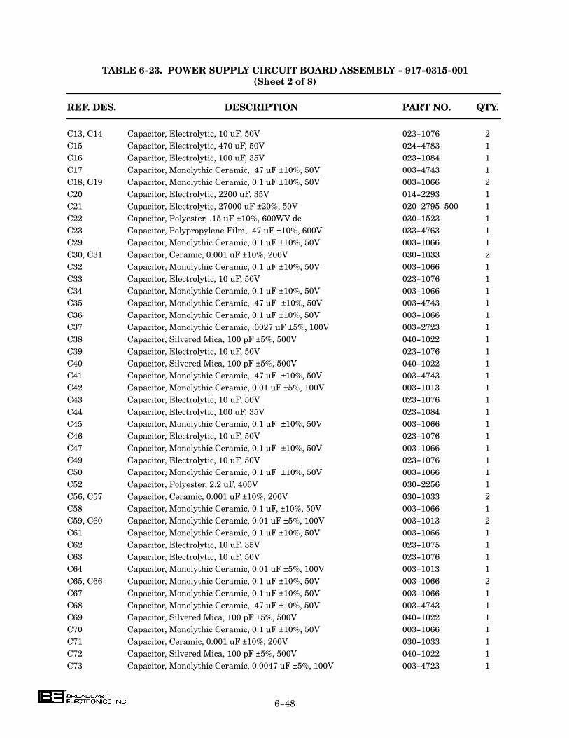
6-48
TABLE 6-23. POWER SUPPLY CIRCUIT BOARD ASSEMBLY - 917-0315-001
(Sheet 2 of 8)
REF. DES. DESCRIPTION PART NO. QTY.
C13, C14 Capacitor, Electrolytic, 10 uF, 50V 023-1076 2
C15 Capacitor, Electrolytic, 470 uF, 50V 024-4783 1
C16 Capacitor, Electrolytic, 100 uF, 35V 023-1084 1
C17 Capacitor, Monolythic Ceramic, .47 uF ±10%, 50V 003-4743 1
C18, C19 Capacitor, Monolythic Ceramic, 0.1 uF ±10%, 50V 003-1066 2
C20 Capacitor, Electrolytic, 2200 uF, 35V 014-2293 1
C21 Capacitor, Electrolytic, 27000 uF ±20%, 50V 020-2795-500 1
C22 Capacitor, Polyester, .15 uF ±10%, 600WV dc 030-1523 1
C23 Capacitor, Polypropylene Film, .47 uF ±10%, 600V 033-4763 1
C29 Capacitor, Monolythic Ceramic, 0.1 uF ±10%, 50V 003-1066 1
C30, C31 Capacitor, Ceramic, 0.001 uF ±10%, 200V 030-1033 2
C32 Capacitor, Monolythic Ceramic, 0.1 uF ±10%, 50V 003-1066 1
C33 Capacitor, Electrolytic, 10 uF, 50V 023-1076 1
C34 Capacitor, Monolythic Ceramic, 0.1 uF ±10%, 50V 003-1066 1
C35 Capacitor, Monolythic Ceramic, .47 uF ±10%, 50V 003-4743 1
C36 Capacitor, Monolythic Ceramic, 0.1 uF ±10%, 50V 003-1066 1
C37 Capacitor, Monolythic Ceramic, .0027 uF ±5%, 100V 003-2723 1
C38 Capacitor, Silvered Mica, 100 pF ±5%, 500V 040-1022 1
C39 Capacitor, Electrolytic, 10 uF, 50V 023-1076 1
C40 Capacitor, Silvered Mica, 100 pF ±5%, 500V 040-1022 1
C41 Capacitor, Monolythic Ceramic, .47 uF ±10%, 50V 003-4743 1
C42 Capacitor, Monolythic Ceramic, 0.01 uF ±5%, 100V 003-1013 1
C43 Capacitor, Electrolytic, 10 uF, 50V 023-1076 1
C44 Capacitor, Electrolytic, 100 uF, 35V 023-1084 1
C45 Capacitor, Monolythic Ceramic, 0.1 uF ±10%, 50V 003-1066 1
C46 Capacitor, Electrolytic, 10 uF, 50V 023-1076 1
C47 Capacitor, Monolythic Ceramic, 0.1 uF ±10%, 50V 003-1066 1
C49 Capacitor, Electrolytic, 10 uF, 50V 023-1076 1
C50 Capacitor, Monolythic Ceramic, 0.1 uF ±10%, 50V 003-1066 1
C52 Capacitor, Polyester, 2.2 uF, 400V 030-2256 1
C56, C57 Capacitor, Ceramic, 0.001 uF ±10%, 200V 030-1033 2
C58 Capacitor, Monolythic Ceramic, 0.1 uF, ±10%, 50V 003-1066 1
C59, C60 Capacitor, Monolythic Ceramic, 0.01 uF ±5%, 100V 003-1013 2
C61 Capacitor, Monolythic Ceramic, 0.1 uF ±10%, 50V 003-1066 1
C62 Capacitor, Electrolytic, 10 uF, 35V 023-1075 1
C63 Capacitor, Electrolytic, 10 uF, 50V 023-1076 1
C64 Capacitor, Monolythic Ceramic, 0.01 uF ±5%, 100V 003-1013 1
C65, C66 Capacitor, Monolythic Ceramic, 0.1 uF ±10%, 50V 003-1066 2
C67 Capacitor, Monolythic Ceramic, 0.1 uF ±10%, 50V 003-1066 1
C68 Capacitor, Monolythic Ceramic, .47 uF ±10%, 50V 003-4743 1
C69 Capacitor, Silvered Mica, 100 pF ±5%, 500V 040-1022 1
C70 Capacitor, Monolythic Ceramic, 0.1 uF ±10%, 50V 003-1066 1
C71 Capacitor, Ceramic, 0.001 uF ±10%, 200V 030-1033 1
C72 Capacitor, Silvered Mica, 100 pF ±5%, 500V 040-1022 1
C73 Capacitor, Monolythic Ceramic, 0.0047 uF ±5%, 100V 003-4723 1
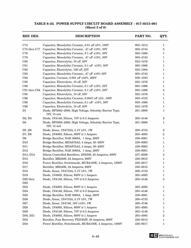
6-49
TABLE 6-23. POWER SUPPLY CIRCUIT BOARD ASSEMBLY - 917-0315-001
(Sheet 3 of 8)
REF. DES. DESCRIPTION PART NO. QTY.
C74 Capacitor, Monolythic Ceramic, 0.01 uF ±5%, 100V 003-1013 1
C75 thru C77 Capacitor, Monolythic Ceramic, .47 uF ±10%, 50V 003-4743 3
C78 Capacitor, Monolythic Ceramic, 0.1 uF ±10%, 50V 003-1066 1
C79 Capacitor, Monolythic Ceramic, .47 uF ±10%, 50V 003-4743 1
C80 Capacitor, Electrolytic, 10 uF, 50V 023-1076 1
C81 Capacitor, Monolythic Ceramic, 0.1 uF ±10%, 50V 003-1066 1
C82 Capacitor, Electrolytic, 100 uF, 35V 023-1084 1
C83 Capacitor, Monolythic Ceramic, .47 uF ±10% 50V 003-4743 1
C84 Capacitor, Ceramic, 0.001 uF ±10%, 200V 030-1033 1
C85 Capacitor, Electrolytic, 10 uF, 50V 023-1076 1
C86 Capacitor, Monolythic Ceramic, 0.1 uF ±10%, 50V 003-1066 1
C91 thru C94 Capacitor, Monolythic Ceramic, 0.1 uF ±10%, 50V 003-1066 4
C95 Capacitor, Electrolytic, 10 uF, 50V 023-1076 1
C96 Capacitor, Monolythic Ceramic, 0.0047 uF ±5%, 100V 003-4723 1
C98 Capacitor, Monolythic Ceramic, 0.1 uF ±10%, 50V 003-1066 1
C99 Capacitor, Electrolytic, 10 uF, 50V 023-1076 1
D1 Diode, HP5082-2800, High Voltage, Schottky Barrier Type, 201-2800 1
70V, 15 mA
D2, D3 Diode, 1N4148, Silicon, 75V @ 0.3 Amperes 203-4148 2
D4 Diode, HP5082-2800, High Voltage, Schottky Barrier Type, 201-2800 1
70V, 15 mA
D5 ,D6 Diode, Zener, 1N4733A, 5.1V ±5%, 1W 200-4733 2
D7, D8 Diode, 1N4005, Silicon, 600V @ 1 Ampere 203-4005 2
D9 Bridge Rectifier, NAE 3060A, 1 Amp, 200V 239-0001 1
D10 Bridge Rectifier, MDA970A3, 4 Amps, 50-200V 239-0003 1
D11 Bridge Rectifier, MDA970A3, 4 Amps, 50-200V 239-0003 1
D12 Bridge Rectifier, NAE 3060A, 1 Amp, 200V 239-0001 1
D13, D14 Silicon Controlled Rectifiers, 2N6508, 25 Amperes, 600V 237-6508 2
D15 Rectifier, MR2406, 24 Amperes, 600V 230-0015 1
D16 Power Rectifier, Switchmode, MUR4100E, 4 Amperes, 1000V 230-0017 1
D17 Rectifier, MR2406, 24 Amperes, 600V 230-0015 1
D18 Diode, Zener, 1N4733A, 5.1V ±5%, 1W 200-4733 1
D19 Diode, 1N4005, Silicon, 600V @ 1 Ampere 203-4005 1
D20 thru Diode, 1N4148, Silicon, 75V @ 0.3 Amperes 203-4148 3
D22
D23 Diode, 1N4005, Silicon, 600V @ 1 Ampere 203-4005 1
D24 Diode, 1N4148, Silicon, 75V @ 0.3 Amperes 203-4148 1
D25 Bridge Rectifier, NAE 3060A, 1 Amp, 200V 239-0001 1
D26 Diode, Zener, 1N4733A, 5.1V ±5%, 1W 200-4733 1
D27 Diode, Zener, 1N4746, 18V ±10%, 1W 200-4746 1
D28 Diode, 1N4005, Silicon, 600V @ 1 Ampere 203-4005 1
D29 Diode, 1N4148, Silicon, 75V @ 0.3 Amperes 203-4148 1
D30, D31 Diode, 1N4005, Silicon, 600V @ 1 Ampere 203-4005 2
D32 Rectifier, Fast Recovery, FEN30JP, 30 Amperes, 600V 230-0013 1
D34 Power Rectifier, Switchmode, MUR4100E, 4 Amperes, 1000V 230-0017 1
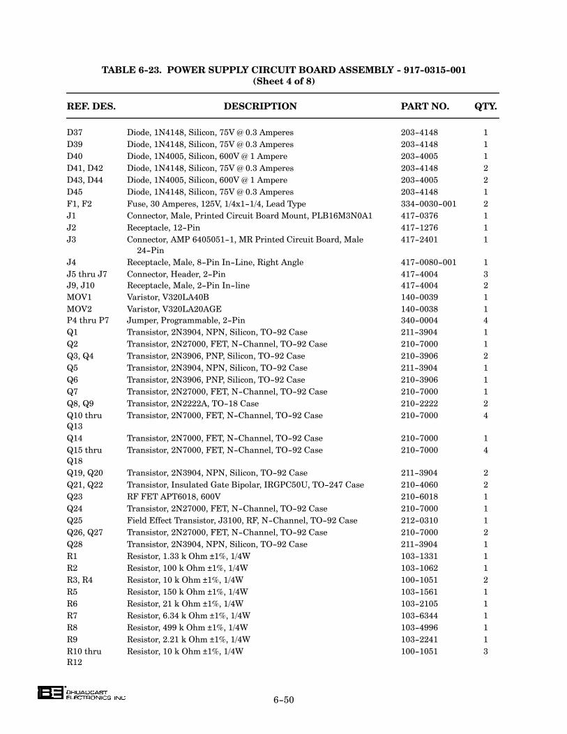
6-50
TABLE 6-23. POWER SUPPLY CIRCUIT BOARD ASSEMBLY - 917-0315-001
(Sheet 4 of 8)
REF. DES. DESCRIPTION PART NO. QTY.
D37 Diode, 1N4148, Silicon, 75V @ 0.3 Amperes 203-4148 1
D39 Diode, 1N4148, Silicon, 75V @ 0.3 Amperes 203-4148 1
D40 Diode, 1N4005, Silicon, 600V @ 1 Ampere 203-4005 1
D41, D42 Diode, 1N4148, Silicon, 75V @ 0.3 Amperes 203-4148 2
D43, D44 Diode, 1N4005, Silicon, 600V @ 1 Ampere 203-4005 2
D45 Diode, 1N4148, Silicon, 75V @ 0.3 Amperes 203-4148 1
F1, F2 Fuse, 30 Amperes, 125V, 1/4x1-1/4, Lead Type 334-0030-001 2
J1 Connector, Male, Printed Circuit Board Mount, PLB16M3N0A1 417-0376 1
J2 Receptacle, 12-Pin 417-1276 1
J3 Connector, AMP 6405051-1, MR Printed Circuit Board, Male 417-2401 1
24-Pin
J4 Receptacle, Male, 8-Pin In-Line, Right Angle 417-0080-001 1
J5 thru J7 Connector, Header, 2-Pin 417-4004 3
J9, J10 Receptacle, Male, 2-Pin In-line 417-4004 2
MOV1 Varistor, V320LA40B 140-0039 1
MOV2 Varistor, V320LA20AGE 140-0038 1
P4 thru P7 Jumper, Programmable, 2-Pin 340-0004 4
Q1 Transistor, 2N3904, NPN, Silicon, TO-92 Case 211-3904 1
Q2 Transistor, 2N27000, FET, N-Channel, TO-92 Case 210-7000 1
Q3, Q4 Transistor, 2N3906, PNP, Silicon, TO-92 Case 210-3906 2
Q5 Transistor, 2N3904, NPN, Silicon, TO-92 Case 211-3904 1
Q6 Transistor, 2N3906, PNP, Silicon, TO-92 Case 210-3906 1
Q7 Transistor, 2N27000, FET, N-Channel, TO-92 Case 210-7000 1
Q8, Q9 Transistor, 2N2222A, TO-18 Case 210-2222 2
Q10 thru Transistor, 2N7000, FET, N-Channel, TO-92 Case 210-7000 4
Q13
Q14 Transistor, 2N7000, FET, N-Channel, TO-92 Case 210-7000 1
Q15 thru Transistor, 2N7000, FET, N-Channel, TO-92 Case 210-7000 4
Q18
Q19, Q20 Transistor, 2N3904, NPN, Silicon, TO-92 Case 211-3904 2
Q21, Q22 Transistor, Insulated Gate Bipolar, IRGPC50U, TO-247 Case 210-4060 2
Q23 RF FET APT6018, 600V 210-6018 1
Q24 Transistor, 2N27000, FET, N-Channel, TO-92 Case 210-7000 1
Q25 Field Effect Transistor, J3100, RF, N-Channel, TO-92 Case 212-0310 1
Q26, Q27 Transistor, 2N27000, FET, N-Channel, TO-92 Case 210-7000 2
Q28 Transistor, 2N3904, NPN, Silicon, TO-92 Case 211-3904 1
R1 Resistor, 1.33 k Ohm ±1%, 1/4W 103-1331 1
R2 Resistor, 100 k Ohm ±1%, 1/4W 103-1062 1
R3, R4 Resistor, 10 k Ohm ±1%, 1/4W 100-1051 2
R5 Resistor, 150 k Ohm ±1%, 1/4W 103-1561 1
R6 Resistor, 21 k Ohm ±1%, 1/4W 103-2105 1
R7 Resistor, 6.34 k Ohm ±1%, 1/4W 103-6344 1
R8 Resistor, 499 k Ohm ±1%, 1/4W 103-4996 1
R9 Resistor, 2.21 k Ohm ±1%, 1/4W 103-2241 1
R10 thru Resistor, 10 k Ohm ±1%, 1/4W 100-1051 3
R12

6-51
TABLE 6-23. POWER SUPPLY CIRCUIT BOARD ASSEMBLY - 917-0315-001
(Sheet 5 of 8)
REF. DES. DESCRIPTION PART NO. QTY.
R13 Resistor, 1 k Ohm ±1%, 1/4W 100-1041 1
R14 Resistor, 20.0 k Ohm ±1%, 1/4W 103-2051 1
R15 Resistor, 100 k Ohm ±1%, 1/4W 103-1062 1
R16 Resistor, 10 k Ohm ±1%, 1/4W 100-1051 1
R17 Resistor, 100 k Ohm ±1%, 1/4W 103-1062 1
R18 Resistor, 10 k Ohm ±1%, 1/4W 100-1051 1
R19 Resistor, 3.3 Meg Ohm ±5%, 1/4W 100-3373 1
R20 Resistor, 100 Ohm ±1%, 1/4W 100-1031 1
R21 Resistor, 866 Ohm ±1%, 1/4W 103-8663 1
R22, R23 Resistor, 1.10 k Ohm ±1%, 1/4W 103-1104 2
R24 Resistor, 51.1 Ohm ±1%, 1/4W 103-5112 1
R25 Resistor, 10 k Ohm ±1%, 1/4W 100-1051 1
R26 Resistor, 5.11 k Ohm ±1%, 1/4W 103-5141 1
R27 Resistor, 1 k Ohm ±1%, 1/4W 100-1041 1
R28 Resistor, 1.33 k Ohm ±1%, 1/4W 103-1331 1
R29, R30 Resistor, 3.32 k Ohm ±1%, 1/4W 103-3324 2
R31 Resistor, 10 k Ohm ±1%, 1/4W 100-1051 1
R32 Resistor, 51.1 Ohm ±1%, 1/4W 103-5112 1
R33 Resistor, 665 Ohm ±1%, 1/4W 103-6653 1
R34 Resistor, 499 k Ohm ±1%, 1/4W 103-4996 1
R35 Resistor, 10 k Ohm ±1%, 1/4W 100-1051 1
R36 Resistor, 10 k Ohm ±1%, 1/4W 100-1051 1
R37, R38 Resistor, 82 Ohm ±5%, 2W 130-8223 2
R39, R40 Resistor, 270 Ohm ±5%, 1/2W 110-2733 2
R41, R42 Resistor, 47 Ohm ±5%, 2W 130-4723 2
R41, R42 Resistor, 68 Ohm ±5%, 2W 132-6832 2
R43 Resistor, 1.33 k Ohm ±1%, 1/4W 103-1331 1
R44 Resistor, 2.21 k Ohm ±1%, 1/4W 103-2241 1
R45 Resistor, 3.3 Meg Ohm ±5%, 1/4W 100-3373 1
R46 Resistor, 100 Ohm ±1%, 1/4W 100-1031 1
R47 Resistor, 1.10 k Ohm ±1%, 1/4W 103-1104 1
R48, R49 Resistor, 47 Ohm ±5%, 2W 130-4723 2
R52 Resistor, 2.21 k Ohm ±1%, 1/4W 103-2241 1
R53 Resistor, 3.3 Meg Ohm ±5%, 1/4W 100-3373 1
R54 Resistor, 10 k Ohm ±1%, 1/4W 100-1051 1
R55 Resistor, 3.3 Meg Ohm ±5%, 1/4W 100-3373 1
R56 Resistor, 10 k Ohm ±1%, 1/4W 100-1051 1
R57 Resistor, 1.33 k Ohm ±1%, 1/4W 103-1331 1
R58 Resistor, 100 k Ohm ±1%, 1/4W 103-1062 1
R59 Resistor, 1.33 k Ohm ±1%, 1/4W 103-1331 1
R60, R61 Resistor, 100 k Ohm ±1%, 1/4W 103-1062 2
R62 Resistor, 10 k Ohm ±1%, 1/4W 100-1051 1
R63 Resistor, 1.33 k Ohm ±1%, 1/4W 103-1331 1
R64 Resistor, 3.3 Meg Ohm ±5%, 1/4W 100-3373 1
R65 Resistor, 1.33 k Ohm ±1%, 1/4W 103-1331 1
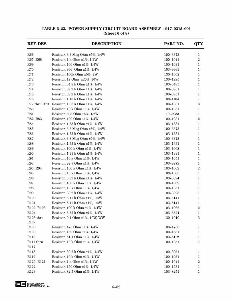
6-52
TABLE 6-23. POWER SUPPLY CIRCUIT BOARD ASSEMBLY - 917-0315-001
(Sheet 6 of 8)
REF. DES. DESCRIPTION PART NO. QTY.
R66 Resistor, 3.3 Meg Ohm ±5%, 1/4W 100-3373 1
R67, R68 Resistor, 1 k Ohm ±1%, 1/4W 100-1041 2
R69 Resistor, 100 Ohm ±1%, 1/4W 100-1031 1
R70 Resistor, 866 Ohm ±1%, 1/4W 103-8663 1
R71 Resistor, 100k Ohm ±5%, 2W 130-1062 1
R72 Resistor, 12 Ohm ±20%, 30W 130-1225 1
R73 Resistor, 34.8 k Ohm ±1%, 1/4W 103-3485 1
R74 Resistor, 39.2 k Ohm ±1%, 1/4W 100-3951 1
R75 Resistor, 39.2 k Ohm ±1%, 1/4W 100-3951 1
R76 Resistor, 1.10 k Ohm ±1%, 1/4W 103-1104 1
R77 thru R79 Resistor, 1.33 k Ohm ±1%, 1/4W 103-1331 3
R80 Resistor, 10 k Ohm ±1%, 1/4W 100-1051 1
R81 Resistor, 393 Ohm ±5%, 1/2W 110-3933 1
R82, R83 Resistor, 100 Ohm ±1%, 1/4W 100-1031 2
R84 Resistor, 1.33 k Ohm ±1%, 1/4W 103-1331 1
R85 Resistor, 3.3 Meg Ohm ±5%, 1/4W 100-3373 1
R86 Resistor, 1.33 k Ohm ±1%, 1/4W 103-1331 1
R87 Resistor, 3.3 Meg Ohm ±5%, 1/4W 100-3373 1
R88 Resistor, 1.33 k Ohm ±1%, 1/4W 103-1331 1
R89 Resistor, 100 k Ohm ±1%, 1/4W 103-1062 1
R90 Resistor, 1.33 k Ohm ±1%, 1/4W 103-1331 1
R91 Resistor, 10 k Ohm ±1%, 1/4W 100-1051 1
R92 Resistor, 88.7 Ohm ±1%, 1/4W 103-8872 1
R93, R94 Resistor, 100 k Ohm ±1%, 1/4W 103-1062 2
R95 Resistor, 13 k Ohm ±1%, 1/4W 103-1305 1
R96 Resistor, 3.32 k Ohm ±1%, 1/4W 103-3324 1
R97 Resistor, 100 k Ohm ±1%, 1/4W 103-1062 1
R98 Resistor, 10 k Ohm ±1%, 1/4W 100-1051 1
R99 Resistor, 33.2 k Ohm ±1%, 1/4W 103-3325 1
R100 Resistor, 5.11 k Ohm ±1%, 1/4W 103-5141 1
R101 Resistor, 5.11 k Ohm ±1%, 1/4W 103-5141 1
R102, R103 Resistor, 100 k Ohm ±1%, 1/4W 103-1062 2
R104 Resistor, 3.32 k Ohm ±1%, 1/4W 103-3324 1
R105 thru Resistor, 0.1 Ohm ±1%, 10W, WW 130-1010 3
R107
R108 Resistor, 475 Ohm ±1%, 1/4W 103-4753 1
R109 Resistor, 162 Ohm ±1%, 1/4W 100-1631 1
R110 Resistor, 51.1 Ohm ±1%, 1/4W 103-5112 1
R111 thru Resistor, 10 k Ohm ±1%, 1/4W 100-1051 7
R117
R118 Resistor, 39.2 k Ohm ±1%, 1/4W 100-3951 1
R119 Resistor, 10 k Ohm ±1%, 1/4W 100-1051 1
R120, R121 Resistor, 1 k Ohm ±1%, 1/4W 100-1041 2
R122 Resistor, 150 Ohm ±1%, 1/4W 100-1531 1
R123 Resistor, 82.5 Ohm ±1%, 1/4W 103-8251 1
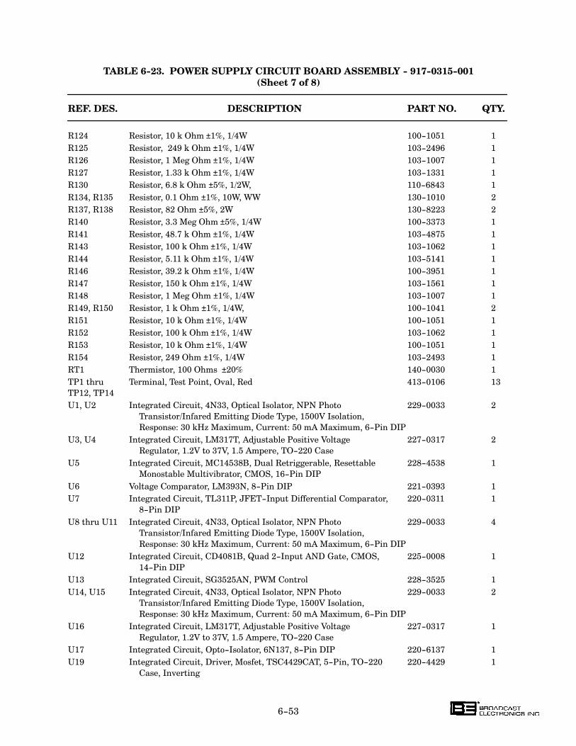
6-53
TABLE 6-23. POWER SUPPLY CIRCUIT BOARD ASSEMBLY - 917-0315-001
(Sheet 7 of 8)
REF. DES. DESCRIPTION PART NO. QTY.
R124 Resistor, 10 k Ohm ±1%, 1/4W 100-1051 1
R125 Resistor, 249 k Ohm ±1%, 1/4W 103-2496 1
R126 Resistor, 1 Meg Ohm ±1%, 1/4W 103-1007 1
R127 Resistor, 1.33 k Ohm ±1%, 1/4W 103-1331 1
R130 Resistor, 6.8 k Ohm ±5%, 1/2W, 110-6843 1
R134, R135 Resistor, 0.1 Ohm ±1%, 10W, WW 130-1010 2
R137, R138 Resistor, 82 Ohm ±5%, 2W 130-8223 2
R140 Resistor, 3.3 Meg Ohm ±5%, 1/4W 100-3373 1
R141 Resistor, 48.7 k Ohm ±1%, 1/4W 103-4875 1
R143 Resistor, 100 k Ohm ±1%, 1/4W 103-1062 1
R144 Resistor, 5.11 k Ohm ±1%, 1/4W 103-5141 1
R146 Resistor, 39.2 k Ohm ±1%, 1/4W 100-3951 1
R147 Resistor, 150 k Ohm ±1%, 1/4W 103-1561 1
R148 Resistor, 1 Meg Ohm ±1%, 1/4W 103-1007 1
R149, R150 Resistor, 1 k Ohm ±1%, 1/4W, 100-1041 2
R151 Resistor, 10 k Ohm ±1%, 1/4W 100-1051 1
R152 Resistor, 100 k Ohm ±1%, 1/4W 103-1062 1
R153 Resistor, 10 k Ohm ±1%, 1/4W 100-1051 1
R154 Resistor, 249 Ohm ±1%, 1/4W 103-2493 1
RT1 Thermistor, 100 Ohms ±20% 140-0030 1
TP1 thru Terminal, Test Point, Oval, Red 413-0106 13
TP12, TP14
U1, U2 Integrated Circuit, 4N33, Optical Isolator, NPN Photo 229-0033 2
Transistor/Infared Emitting Diode Type, 1500V Isolation,
Response: 30 kHz Maximum, Current: 50 mA Maximum, 6-Pin DIP
U3, U4 Integrated Circuit, LM317T, Adjustable Positive Voltage 227-0317 2
Regulator, 1.2V to 37V, 1.5 Ampere, TO-220 Case
U5 Integrated Circuit, MC14538B, Dual Retriggerable, Resettable 228-4538 1
Monostable Multivibrator, CMOS, 16-Pin DIP
U6 Voltage Comparator, LM393N, 8-Pin DIP 221-0393 1
U7 Integrated Circuit, TL311P, JFET-Input Differential Comparator, 220-0311 1
8-Pin DIP
U8 thru U11 Integrated Circuit, 4N33, Optical Isolator, NPN Photo 229-0033 4
Transistor/Infared Emitting Diode Type, 1500V Isolation,
Response: 30 kHz Maximum, Current: 50 mA Maximum, 6-Pin DIP
U12 Integrated Circuit, CD4081B, Quad 2-Input AND Gate, CMOS, 225-0008 1
14-Pin DIP
U13 Integrated Circuit, SG3525AN, PWM Control 228-3525 1
U14, U15 Integrated Circuit, 4N33, Optical Isolator, NPN Photo 229-0033 2
Transistor/Infared Emitting Diode Type, 1500V Isolation,
Response: 30 kHz Maximum, Current: 50 mA Maximum, 6-Pin DIP
U16 Integrated Circuit, LM317T, Adjustable Positive Voltage 227-0317 1
Regulator, 1.2V to 37V, 1.5 Ampere, TO-220 Case
U17 Integrated Circuit, Opto-Isolator, 6N137, 8-Pin DIP 220-6137 1
U19 Integrated Circuit, Driver, Mosfet, TSC4429CAT, 5-Pin, TO-220 220-4429 1
Case, Inverting

6-54
TABLE 6-23. POWER SUPPLY CIRCUIT BOARD ASSEMBLY - 917-0315-001
(Sheet 8 of 8)
REF. DES. DESCRIPTION PART NO. QTY.
U21 Integrated Circuit, MC14093B, Quad 2-Input NAND Schmitt Trigger, 220-4093 1
CMOS, 14-Pin DIP
U22 Integrated Circuit, Opto-Isolator, 6N137, 8-Pin DIP 220-6137 1
U23 Voltage Comparator, LM393N, 8-Pin DIP 221-0393 1
U24 Integrated Circuit, TLO74CN, Quad JFET-Input Operational 221-0074 1
Amplifier, 14-Pin DIP
U25 Temperature Sensor Chip, TMP01FP, 8-Pin DIP 229-1750 1
XU1, XU2 Socket, 6-Pin DIP 417-0600 2
XU5 Socket, 16-Pin DIP 417-1604 1
XU6, XU7 Socket, 8-Pin DIP 417-0804 2
XU8 thru Socket, 6-Pin DIP 417-0600 4
XU11
XU12 Socket, 14-Pin DIP 417-1404 1
XU13 Socket, 16-Pin DIP 417-1604 1
XU14, XU15 Socket, 6-Pin DIP 417-0600 2
XU17 Socket, 8-Pin DIP 417-0804 1
XU21 Socket, 14-Pin DIP 417-1404 1
XU22, XU23 Socket, 8-Pin DIP 417-0804 2
XU24 Socket, 14-Pin DIP 417-1404 1
XU25 Socket, 8-Pin DIP 417-0804 1
---- Fuse Clips, AGC 415-2068 4
---- Blank, Power Supply Circuit Board 517-0315-001 1
TABLE 6-24. POWER SUPPLY BULK CAPACITOR CIRCUIT BOARD ASSEMBLY -
917-0315-003
REF. DES. DESCRIPTION PART NO. QTY.
C24, C25 Capacitor, Electrolytic, 1500 uF, 400V dc - 450V dc 013-1500 2
C28 Capacitor, Polypropylene Film, .47 uF ±10%, 600V 033-4763 1
R50 Resistor, 100 k Ohm ±5%, 2W 130-1062 1
R51 Resistor, 36 Ohm ±5%, 2W 130-3623 1
R129 Resistor, 470 k Ohm ±5%, 1/2W 110-4763 1
---- Blank, Power Supply Bulk Capacitor Circuit Board 517-0315-002 1
TABLE 6-25. POWER SUPPLY CAPACITOR CIRCUIT BOARD ASSEMBLY - 917-0315-005
REF. DES. DESCRIPTION PART NO. QTY.
C88, C89 Capacitor, Electrolytic, 7200 uF, 200WV dc 014-7200 2
MOV3 Metal Oxide Varistor, V130LA10A, 130V ac RMS, 10 Joules 140-0006 1
---- Blank, Power Supply Capacitor Circuit Board 517-0315-004 1
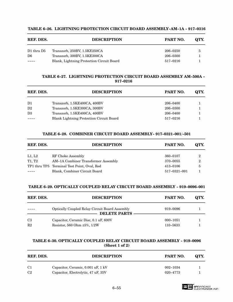
6-55
TABLE 6-26. LIGHTNING PROTECTION CIRCUIT BOARD ASSEMBLY-AM-1A - 917-0316
REF. DES. DESCRIPTION PART NO. QTY.
D1 thru D5 Transzorb, 250BV, 1.5KE250CA 206-0250 5
D6 Transzorb, 300BV, 1.5KE300CA 206-0300 1
---- Blank, Lightning Protection Circuit Board 517-0216 1
TABLE 6-27. LIGHTNING PROTECTION CIRCUIT BOARD ASSEMBLY AM-500A -
917-0216
REF. DES. DESCRIPTION PART NO. QTY.
D1 Transzorb, 1.5KE400CA, 400BV 206-0400 1
D2 Transzorb, 1.5KE300CA, 300BV 206-0300 1
D3 Transzorb, 1.5KE400CA, 400BV 206-0400 1
---- Blank Lightning Protection Circuit Board 517-0216 1
TABLE 6-28. COMBINER CIRCUIT BOARD ASSEMBLY- 917-0321-001/-501
REF. DES. DESCRIPTION PART NO. QTY.
L1, L2 RF Choke Assembly 360-0107 2
T1, T2 AM-1A Combiner Transformer Assembly 370-0055 2
TP1 thru TP5 Terminal Test Point, Oval, Red 413-0106 5
---- Blank, Combiner Circuit Board 517-0321-001 1
TABLE 6-29. OPTICALLY COUPLED RELAY CIRCUIT BOARD ASSEMBLY - 919-0096-001
REF. DES. DESCRIPTION PART NO. QTY.
---- Optically Coupled Relay Circuit Board Assembly 919-0096 1
DELETE PARTS
C3 Capacitor, Ceramic Disc, 0.1 uF, 600V 000-1051 1
R2 Resistor, 560 Ohm ±5%, 1/2W 110-5633 1
TABLE 6-30. OPTICALLY COUPLED RELAY CIRCUIT BOARD ASSEMBLY - 919-0096
(Sheet 1 of 2)
REF. DES. DESCRIPTION PART NO. QTY.
C1 Capacitor, Ceramic, 0.001 uF, 1 kV 002-1034 1
C2 Capacitor, Electrolytic, 47 uF, 35V 020-4773 1
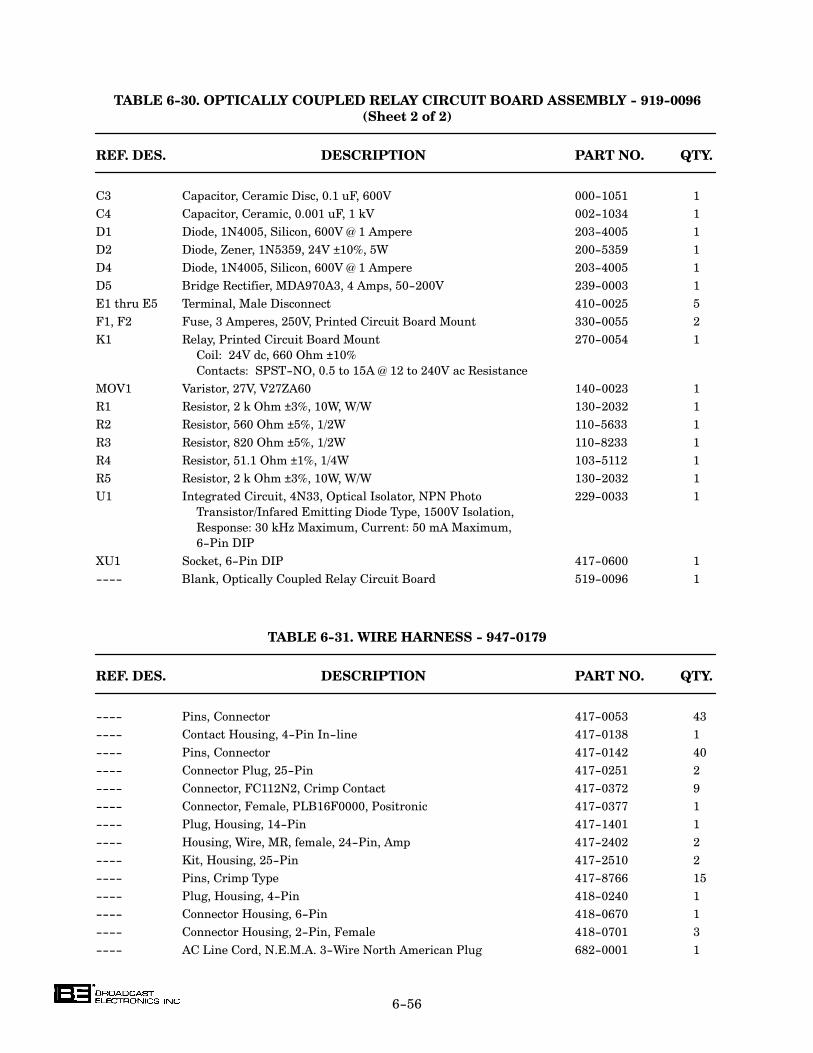
6-56
TABLE 6-30. OPTICALLY COUPLED RELAY CIRCUIT BOARD ASSEMBLY - 919-0096
(Sheet 2 of 2)
REF. DES. DESCRIPTION PART NO. QTY.
C3 Capacitor, Ceramic Disc, 0.1 uF, 600V 000-1051 1
C4 Capacitor, Ceramic, 0.001 uF, 1 kV 002-1034 1
D1 Diode, 1N4005, Silicon, 600V @ 1 Ampere 203-4005 1
D2 Diode, Zener, 1N5359, 24V ±10%, 5W 200-5359 1
D4 Diode, 1N4005, Silicon, 600V @ 1 Ampere 203-4005 1
D5 Bridge Rectifier, MDA970A3, 4 Amps, 50-200V 239-0003 1
E1 thru E5 Terminal, Male Disconnect 410-0025 5
F1, F2 Fuse, 3 Amperes, 250V, Printed Circuit Board Mount 330-0055 2
K1 Relay, Printed Circuit Board Mount 270-0054 1
Coil: 24V dc, 660 Ohm ±10%
Contacts: SPST-NO, 0.5 to 15A @ 12 to 240V ac Resistance
MOV1 Varistor, 27V, V27ZA60 140-0023 1
R1 Resistor, 2 k Ohm ±3%, 10W, W/W 130-2032 1
R2 Resistor, 560 Ohm ±5%, 1/2W 110-5633 1
R3 Resistor, 820 Ohm ±5%, 1/2W 110-8233 1
R4 Resistor, 51.1 Ohm ±1%, 1/4W 103-5112 1
R5 Resistor, 2 k Ohm ±3%, 10W, W/W 130-2032 1
U1 Integrated Circuit, 4N33, Optical Isolator, NPN Photo 229-0033 1
Transistor/Infared Emitting Diode Type, 1500V Isolation,
Response: 30 kHz Maximum, Current: 50 mA Maximum,
6-Pin DIP
XU1 Socket, 6-Pin DIP 417-0600 1
---- Blank, Optically Coupled Relay Circuit Board 519-0096 1
TABLE 6-31. WIRE HARNESS - 947-0179
REF. DES. DESCRIPTION PART NO. QTY.
---- Pins, Connector 417-0053 43
---- Contact Housing, 4-Pin In-line 417-0138 1
---- Pins, Connector 417-0142 40
---- Connector Plug, 25-Pin 417-0251 2
---- Connector, FC112N2, Crimp Contact 417-0372 9
---- Connector, Female, PLB16F0000, Positronic 417-0377 1
---- Plug, Housing, 14-Pin 417-1401 1
---- Housing, Wire, MR, female, 24-Pin, Amp 417-2402 2
---- Kit, Housing, 25-Pin 417-2510 2
---- Pins, Crimp Type 417-8766 15
---- Plug, Housing, 4-Pin 418-0240 1
---- Connector Housing, 6-Pin 418-0670 1
---- Connector Housing, 2-Pin, Female 418-0701 3
---- AC Line Cord, N.E.M.A. 3-Wire North American Plug 682-0001 1
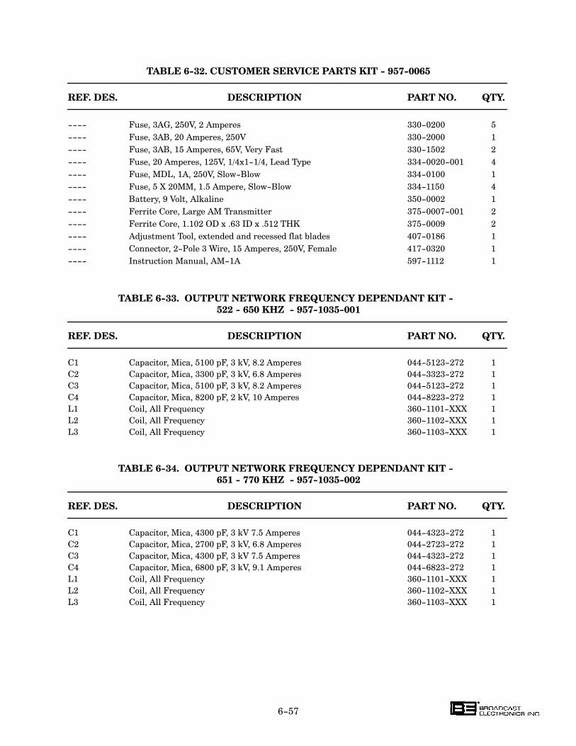
6-57
TABLE 6-32. CUSTOMER SERVICE PARTS KIT - 957-0065
REF. DES. DESCRIPTION PART NO. QTY.
---- Fuse, 3AG, 250V, 2 Amperes 330-0200 5
---- Fuse, 3AB, 20 Amperes, 250V 330-2000 1
---- Fuse, 3AB, 15 Amperes, 65V, Very Fast 330-1502 2
---- Fuse, 20 Amperes, 125V, 1/4x1-1/4, Lead Type 334-0020-001 4
---- Fuse, MDL, 1A, 250V, Slow-Blow 334-0100 1
---- Fuse, 5 X 20MM, 1.5 Ampere, Slow-Blow 334-1150 4
---- Battery, 9 Volt, Alkaline 350-0002 1
---- Ferrite Core, Large AM Transmitter 375-0007-001 2
---- Ferrite Core, 1.102 OD x .63 ID x .512 THK 375-0009 2
---- Adjustment Tool, extended and recessed flat blades 407-0186 1
---- Connector, 2-Pole 3 Wire, 15 Amperes, 250V, Female 417-0320 1
---- Instruction Manual, AM-1A 597-1112 1
TABLE 6-33. OUTPUT NETWORK FREQUENCY DEPENDANT KIT -
522 - 650 KHZ - 957-1035-001
REF. DES. DESCRIPTION PART NO. QTY.
C1 Capacitor, Mica, 5100 pF, 3 kV, 8.2 Amperes 044-5123-272 1
C2 Capacitor, Mica, 3300 pF, 3 kV, 6.8 Amperes 044-3323-272 1
C3 Capacitor, Mica, 5100 pF, 3 kV, 8.2 Amperes 044-5123-272 1
C4 Capacitor, Mica, 8200 pF, 2 kV, 10 Amperes 044-8223-272 1
L1 Coil, All Frequency 360-1101-XXX 1
L2 Coil, All Frequency 360-1102-XXX 1
L3 Coil, All Frequency 360-1103-XXX 1
TABLE 6-34. OUTPUT NETWORK FREQUENCY DEPENDANT KIT -
651 - 770 KHZ - 957-1035-002
REF. DES. DESCRIPTION PART NO. QTY.
C1 Capacitor, Mica, 4300 pF, 3 kV 7.5 Amperes 044-4323-272 1
C2 Capacitor, Mica, 2700 pF, 3 kV, 6.8 Amperes 044-2723-272 1
C3 Capacitor, Mica, 4300 pF, 3 kV 7.5 Amperes 044-4323-272 1
C4 Capacitor, Mica, 6800 pF, 3 kV, 9.1 Amperes 044-6823-272 1
L1 Coil, All Frequency 360-1101-XXX 1
L2 Coil, All Frequency 360-1102-XXX 1
L3 Coil, All Frequency 360-1103-XXX 1
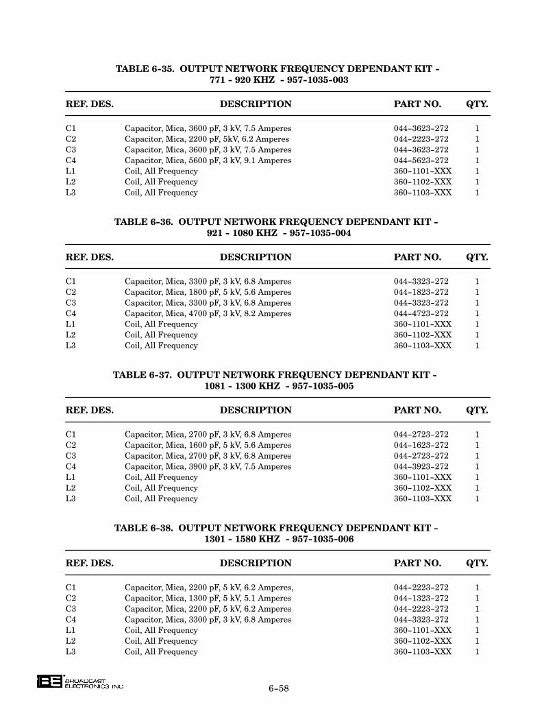
6-58
TABLE 6-35. OUTPUT NETWORK FREQUENCY DEPENDANT KIT -
771 - 920 KHZ - 957-1035-003
REF. DES. DESCRIPTION PART NO. QTY.
C1 Capacitor, Mica, 3600 pF, 3 kV, 7.5 Amperes 044-3623-272 1
C2 Capacitor, Mica, 2200 pF, 5kV, 6.2 Amperes 044-2223-272 1
C3 Capacitor, Mica, 3600 pF, 3 kV, 7.5 Amperes 044-3623-272 1
C4 Capacitor, Mica, 5600 pF, 3 kV, 9.1 Amperes 044-5623-272 1
L1 Coil, All Frequency 360-1101-XXX 1
L2 Coil, All Frequency 360-1102-XXX 1
L3 Coil, All Frequency 360-1103-XXX 1
TABLE 6-36. OUTPUT NETWORK FREQUENCY DEPENDANT KIT -
921 - 1080 KHZ - 957-1035-004
REF. DES. DESCRIPTION PART NO. QTY.
C1 Capacitor, Mica, 3300 pF, 3 kV, 6.8 Amperes 044-3323-272 1
C2 Capacitor, Mica, 1800 pF, 5 kV, 5.6 Amperes 044-1823-272 1
C3 Capacitor, Mica, 3300 pF, 3 kV, 6.8 Amperes 044-3323-272 1
C4 Capacitor, Mica, 4700 pF, 3 kV, 8.2 Amperes 044-4723-272 1
L1 Coil, All Frequency 360-1101-XXX 1
L2 Coil, All Frequency 360-1102-XXX 1
L3 Coil, All Frequency 360-1103-XXX 1
TABLE 6-37. OUTPUT NETWORK FREQUENCY DEPENDANT KIT -
1081 - 1300 KHZ - 957-1035-005
REF. DES. DESCRIPTION PART NO. QTY.
C1 Capacitor, Mica, 2700 pF, 3 kV, 6.8 Amperes 044-2723-272 1
C2 Capacitor, Mica, 1600 pF, 5 kV, 5.6 Amperes 044-1623-272 1
C3 Capacitor, Mica, 2700 pF, 3 kV, 6.8 Amperes 044-2723-272 1
C4 Capacitor, Mica, 3900 pF, 3 kV, 7.5 Amperes 044-3923-272 1
L1 Coil, All Frequency 360-1101-XXX 1
L2 Coil, All Frequency 360-1102-XXX 1
L3 Coil, All Frequency 360-1103-XXX 1
TABLE 6-38. OUTPUT NETWORK FREQUENCY DEPENDANT KIT -
1301 - 1580 KHZ - 957-1035-006
REF. DES. DESCRIPTION PART NO. QTY.
C1 Capacitor, Mica, 2200 pF, 5 kV, 6.2 Amperes, 044-2223-272 1
C2 Capacitor, Mica, 1300 pF, 5 kV, 5.1 Amperes 044-1323-272 1
C3 Capacitor, Mica, 2200 pF, 5 kV, 6.2 Amperes 044-2223-272 1
C4 Capacitor, Mica, 3300 pF, 3 kV, 6.8 Amperes 044-3323-272 1
L1 Coil, All Frequency 360-1101-XXX 1
L2 Coil, All Frequency 360-1102-XXX 1
L3 Coil, All Frequency 360-1103-XXX 1
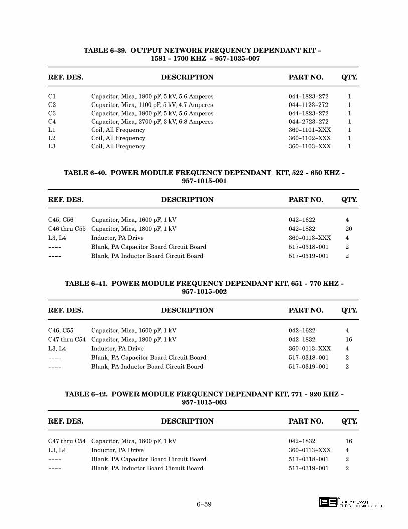
6-59
TABLE 6-39. OUTPUT NETWORK FREQUENCY DEPENDANT KIT -
1581 - 1700 KHZ - 957-1035-007
REF. DES. DESCRIPTION PART NO. QTY.
C1 Capacitor, Mica, 1800 pF, 5 kV, 5.6 Amperes 044-1823-272 1
C2 Capacitor, Mica, 1100 pF, 5 kV, 4.7 Amperes 044-1123-272 1
C3 Capacitor, Mica, 1800 pF, 5 kV, 5.6 Amperes 044-1823-272 1
C4 Capacitor, Mica, 2700 pF, 3 kV, 6.8 Amperes 044-2723-272 1
L1 Coil, All Frequency 360-1101-XXX 1
L2 Coil, All Frequency 360-1102-XXX 1
L3 Coil, All Frequency 360-1103-XXX 1
TABLE 6-40. POWER MODULE FREQUENCY DEPENDANT KIT, 522 - 650 KHZ -
957-1015-001
REF. DES. DESCRIPTION PART NO. QTY.
C45, C56 Capacitor, Mica, 1600 pF, 1 kV 042-1622 4
C46 thru C55 Capacitor, Mica, 1800 pF, 1 kV 042-1832 20
L3, L4 Inductor, PA Drive 360-0113-XXX 4
---- Blank, PA Capacitor Board Circuit Board 517-0318-001 2
---- Blank, PA Inductor Board Circuit Board 517-0319-001 2
TABLE 6-41. POWER MODULE FREQUENCY DEPENDANT KIT, 651 - 770 KHZ -
957-1015-002
REF. DES. DESCRIPTION PART NO. QTY.
C46, C55 Capacitor, Mica, 1600 pF, 1 kV 042-1622 4
C47 thru C54 Capacitor, Mica, 1800 pF, 1 kV 042-1832 16
L3, L4 Inductor, PA Drive 360-0113-XXX 4
---- Blank, PA Capacitor Board Circuit Board 517-0318-001 2
---- Blank, PA Inductor Board Circuit Board 517-0319-001 2
TABLE 6-42. POWER MODULE FREQUENCY DEPENDANT KIT, 771 - 920 KHZ -
957-1015-003
REF. DES. DESCRIPTION PART NO. QTY.
C47 thru C54 Capacitor, Mica, 1800 pF, 1 kV 042-1832 16
L3, L4 Inductor, PA Drive 360-0113-XXX 4
---- Blank, PA Capacitor Board Circuit Board 517-0318-001 2
---- Blank, PA Inductor Board Circuit Board 517-0319-001 2
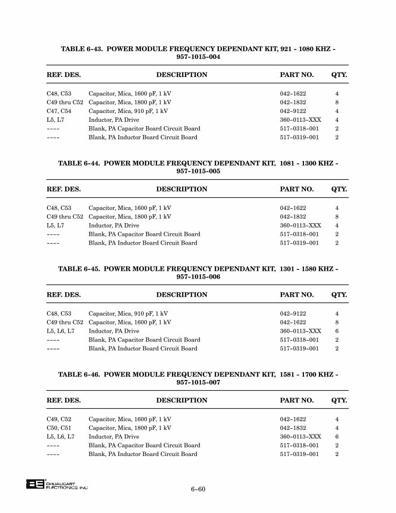
6-60
TABLE 6-43. POWER MODULE FREQUENCY DEPENDANT KIT, 921 - 1080 KHZ -
957-1015-004
REF. DES. DESCRIPTION PART NO. QTY.
C48, C53 Capacitor, Mica, 1600 pF, 1 kV 042-1622 4
C49 thru C52 Capacitor, Mica, 1800 pF, 1 kV 042-1832 8
C47, C54 Capacitor, Mica, 910 pF, 1 kV 042-9122 4
L5, L7 Inductor, PA Drive 360-0113-XXX 4
---- Blank, PA Capacitor Board Circuit Board 517-0318-001 2
---- Blank, PA Inductor Board Circuit Board 517-0319-001 2
TABLE 6-44. POWER MODULE FREQUENCY DEPENDANT KIT, 1081 - 1300 KHZ -
957-1015-005
REF. DES. DESCRIPTION PART NO. QTY.
C48, C53 Capacitor, Mica, 1600 pF, 1 kV 042-1622 4
C49 thru C52 Capacitor, Mica, 1800 pF, 1 kV 042-1832 8
L5, L7 Inductor, PA Drive 360-0113-XXX 4
---- Blank, PA Capacitor Board Circuit Board 517-0318-001 2
---- Blank, PA Inductor Board Circuit Board 517-0319-001 2
TABLE 6-45. POWER MODULE FREQUENCY DEPENDANT KIT, 1301 - 1580 KHZ -
957-1015-006
REF. DES. DESCRIPTION PART NO. QTY.
C48, C53 Capacitor, Mica, 910 pF, 1 kV 042-9122 4
C49 thru C52 Capacitor, Mica, 1600 pF, 1 kV 042-1622 8
L5, L6, L7 Inductor, PA Drive 360-0113-XXX 6
---- Blank, PA Capacitor Board Circuit Board 517-0318-001 2
---- Blank, PA Inductor Board Circuit Board 517-0319-001 2
TABLE 6-46. POWER MODULE FREQUENCY DEPENDANT KIT, 1581 - 1700 KHZ -
957-1015-007
REF. DES. DESCRIPTION PART NO. QTY.
C49, C52 Capacitor, Mica, 1600 pF, 1 kV 042-1622 4
C50, C51 Capacitor, Mica, 1800 pF, 1 kV 042-1832 4
L5, L6, L7 Inductor, PA Drive 360-0113-XXX 6
---- Blank, PA Capacitor Board Circuit Board 517-0318-001 2
---- Blank, PA Inductor Board Circuit Board 517-0319-001 2
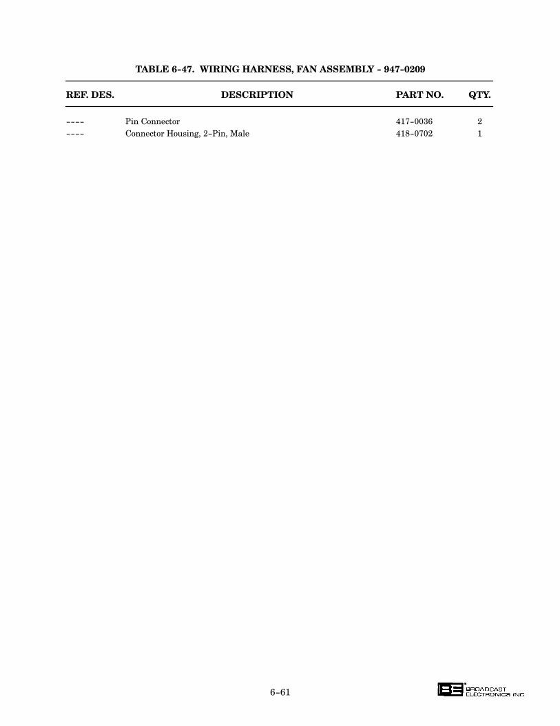
6-61
TABLE 6-47. WIRING HARNESS, FAN ASSEMBLY - 947-0209
REF. DES. DESCRIPTION PART NO. QTY.
---- Pin Connector 417-0036 2
---- Connector Housing, 2-Pin, Male 418-0702 1

7-1
SECTION VII
DRAWINGS
7-1. INTRODUCTION.
7-2. This section provides schematic diagrams and assembly diagrams as indexed below for the
Broadcast Electronics AM-1A transmitter.
FIGURE TITLE NUMBER
7-1 OVERALL SCHEMATIC DIAGRAM, AM-1A/AM-500A SB907-1000-001/
TRANSMITTER 907-0500-001
7-2 SCHEMATIC DIAGRAM, POWER AMPLIFIER SB917-0303/-001
MOTHERBOARD AND COMBINER /-501
7-3 ASSEMBLY DIAGRAM, POWER AMPLIFIER MOTHERBOARD AC917-0303/-001
AND COMBINER /-501
7-4 SCHEMATIC DIAGRAM, OPTICALLY COUPLED RELAY SB919-0096-001
7-5 ASSEMBLY DIAGRAM, OPTICALLY COUPLED AB919-0096-001
RELAY (OCR)
7-6 SCHEMATIC DIAGRAM, POWER SUPPLY CIRCUIT BOARD SB917-0315-001
/-002/-003/-004
/-005
7-7 ASSEMBLY DIAGRAM, POWER SUPPLY CIRCUIT BOARD AC917-0315-001
/-002/-003/-004
/-005
7-8 SCHEMATIC DIAGRAM, MODULATOR CIRCUIT BOARD SB917-0302/-001
/-500
7-9 ASSEMBLY DIAGRAM, MODULATOR CIRCUIT BOARD AD917-0302/-001
/-500
7-10 SCHEMATIC DIAGRAM, POWER AMPLIFIER CIRCUIT SB917-0304
BOARD
7-11 ASSEMBLY DIAGRAM, POWER AMPLIFIER CIRCUIT AD917-0304
BOARD
7-12 SCHEMATIC DIAGRAM, AC SAMPLE CIRCUIT BOARD SA917-0306-007
7-13 SCHEMATIC DIAGRAM, TEMPERATURE SENSOR SA917-0306-009
7-14 SCHEMATIC DIAGRAM, DIRECTIONAL COUPLER SB917-0306-002
CIRCUIT BOARD
7-15 SCHEMATIC DIAGRAM, LIGHTNING DETECTOR SB917-0306-004
CIRCUIT BOARD /-014
7-16 SCHEMATIC DIAGRAM, ECU DISPLAY/CONTROLLER SB917-0306-001
SWITCH CIRCUIT BOARD
7-17 SCHEMATIC DIAGRAM, ECU METER SWITCH SB917-0306-005
CIRCUIT BOARD
7-18 ASSEMBLY DIAGRAM, ECU BREAK-AWAY CIRCUIT BOARD AD917-0306-001
/-002/-003/-004
/-005/-006/-007
/-009/-014
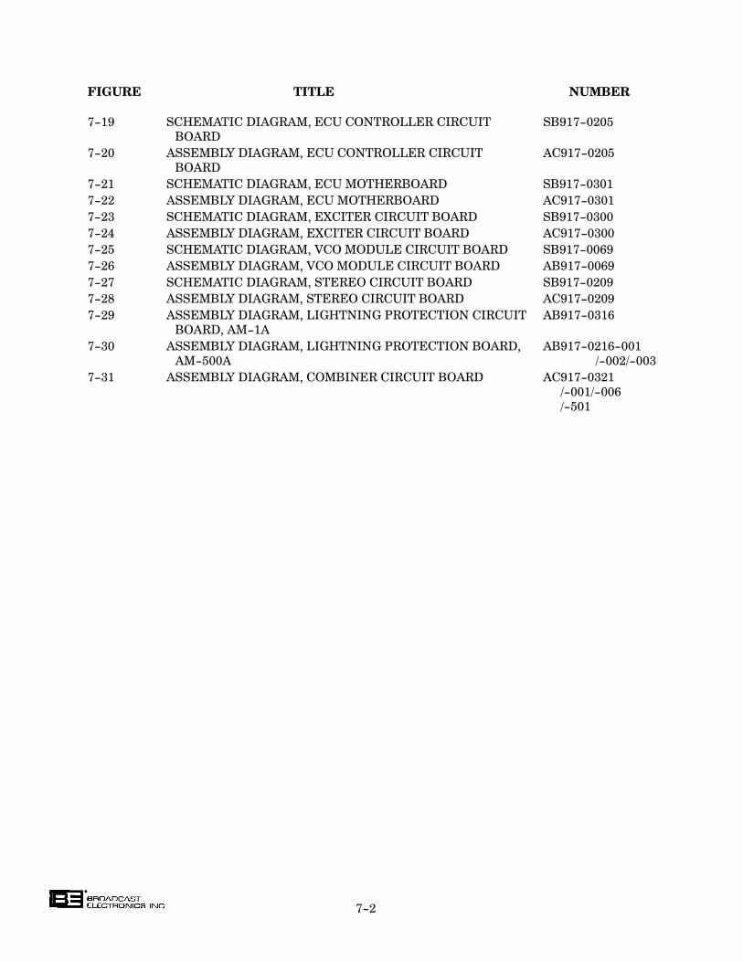
7-2
FIGURE TITLE NUMBER
7-19 SCHEMATIC DIAGRAM, ECU CONTROLLER CIRCUIT SB917-0205
BOARD
7-20 ASSEMBLY DIAGRAM, ECU CONTROLLER CIRCUIT AC917-0205
BOARD
7-21 SCHEMATIC DIAGRAM, ECU MOTHERBOARD SB917-0301
7-22 ASSEMBLY DIAGRAM, ECU MOTHERBOARD AC917-0301
7-23 SCHEMATIC DIAGRAM, EXCITER CIRCUIT BOARD SB917-0300
7-24 ASSEMBLY DIAGRAM, EXCITER CIRCUIT BOARD AC917-0300
7-25 SCHEMATIC DIAGRAM, VCO MODULE CIRCUIT BOARD SB917-0069
7-26 ASSEMBLY DIAGRAM, VCO MODULE CIRCUIT BOARD AB917-0069
7-27 SCHEMATIC DIAGRAM, STEREO CIRCUIT BOARD SB917-0209
7-28 ASSEMBLY DIAGRAM, STEREO CIRCUIT BOARD AC917-0209
7-29 ASSEMBLY DIAGRAM, LIGHTNING PROTECTION CIRCUIT AB917-0316
BOARD, AM-1A
7-30 ASSEMBLY DIAGRAM, LIGHTNING PROTECTION BOARD, AB917-0216-001
AM-500A /-002/-003
7-31 ASSEMBLY DIAGRAM, COMBINER CIRCUIT BOARD AC917-0321
/-001/-006
/-501
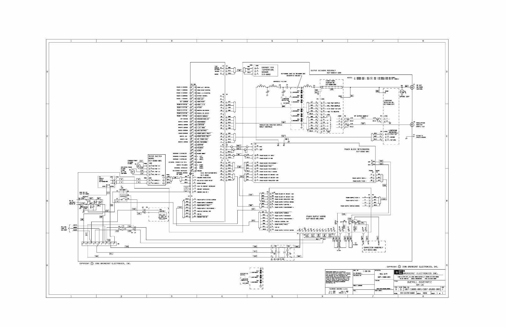
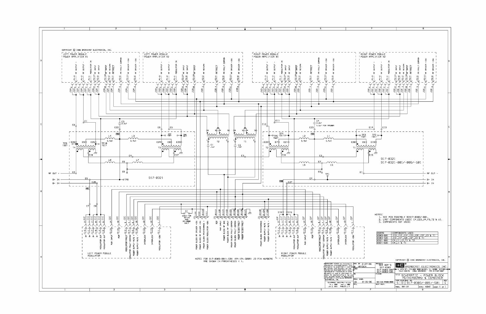


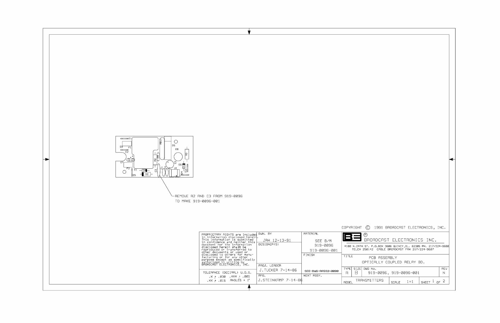
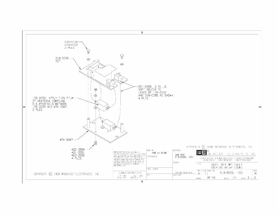

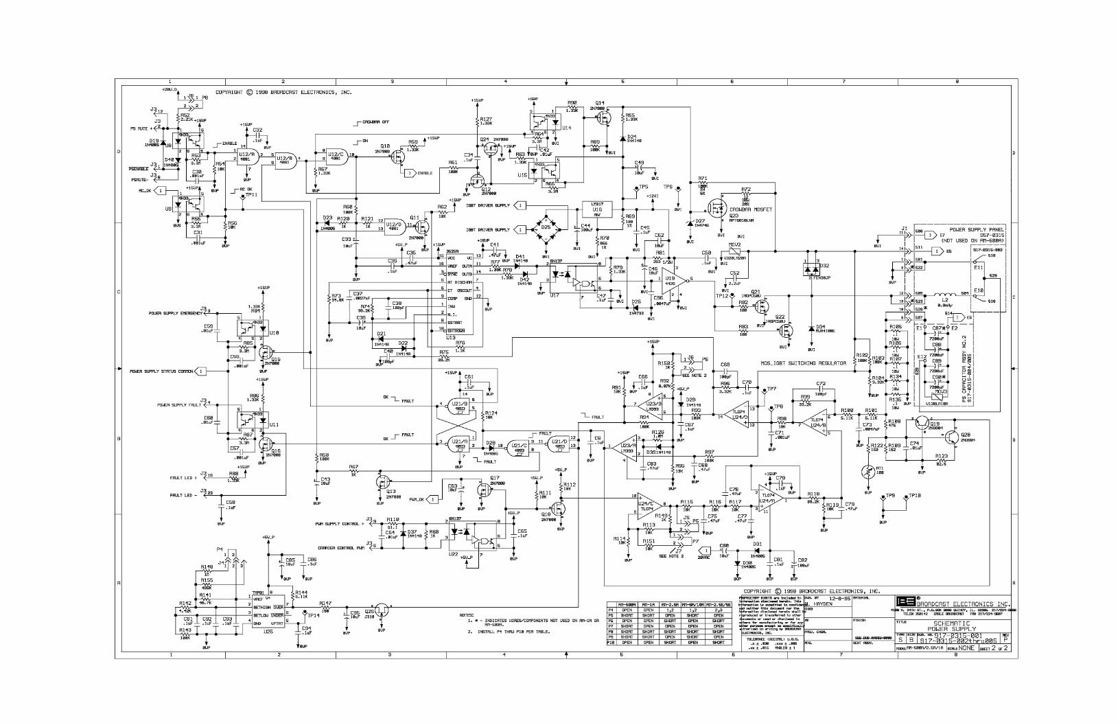
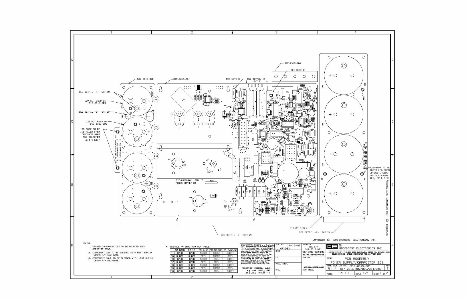
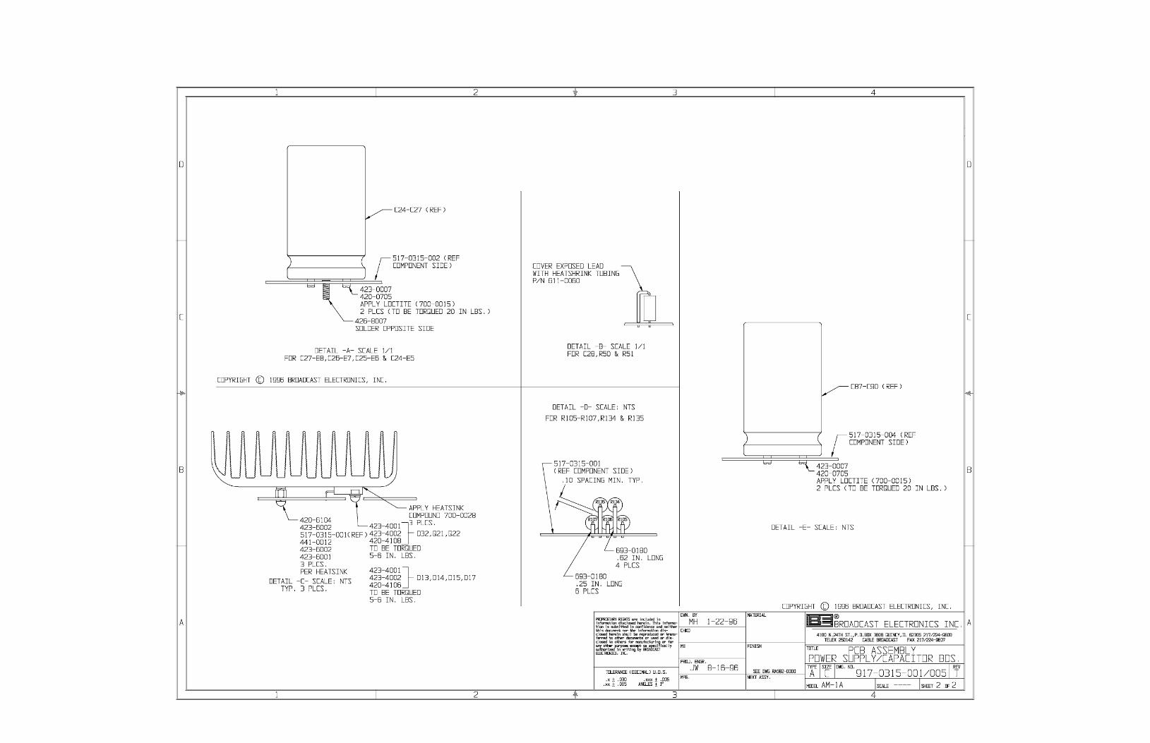
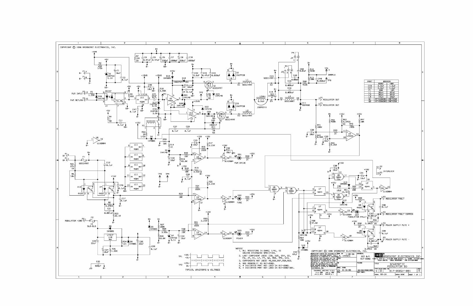
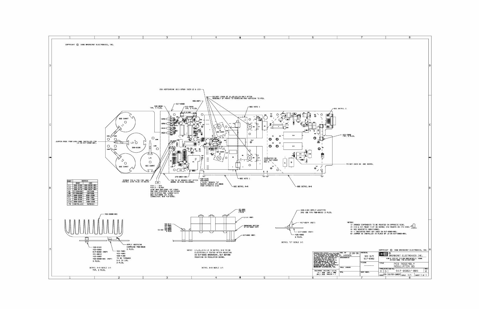
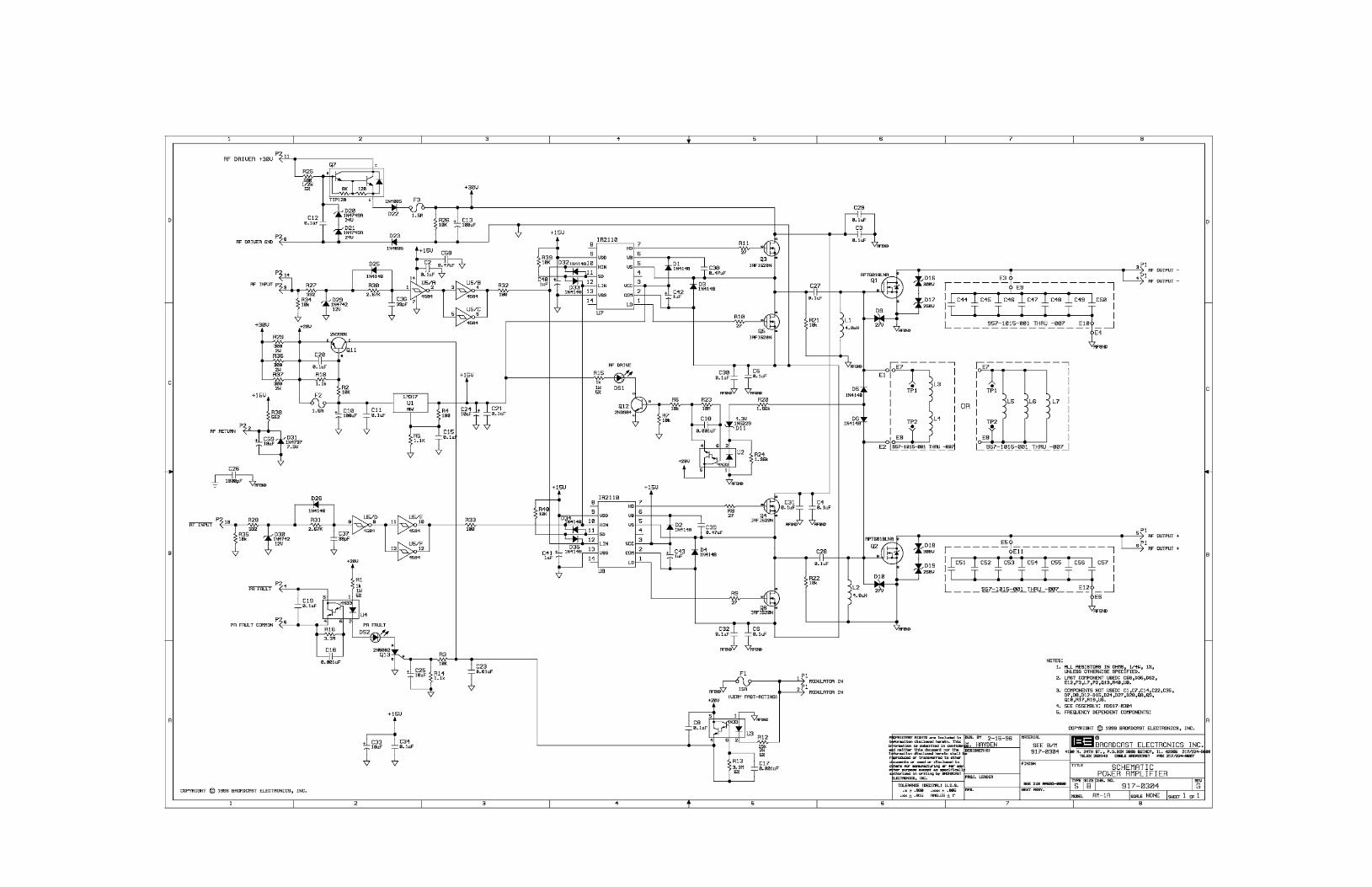
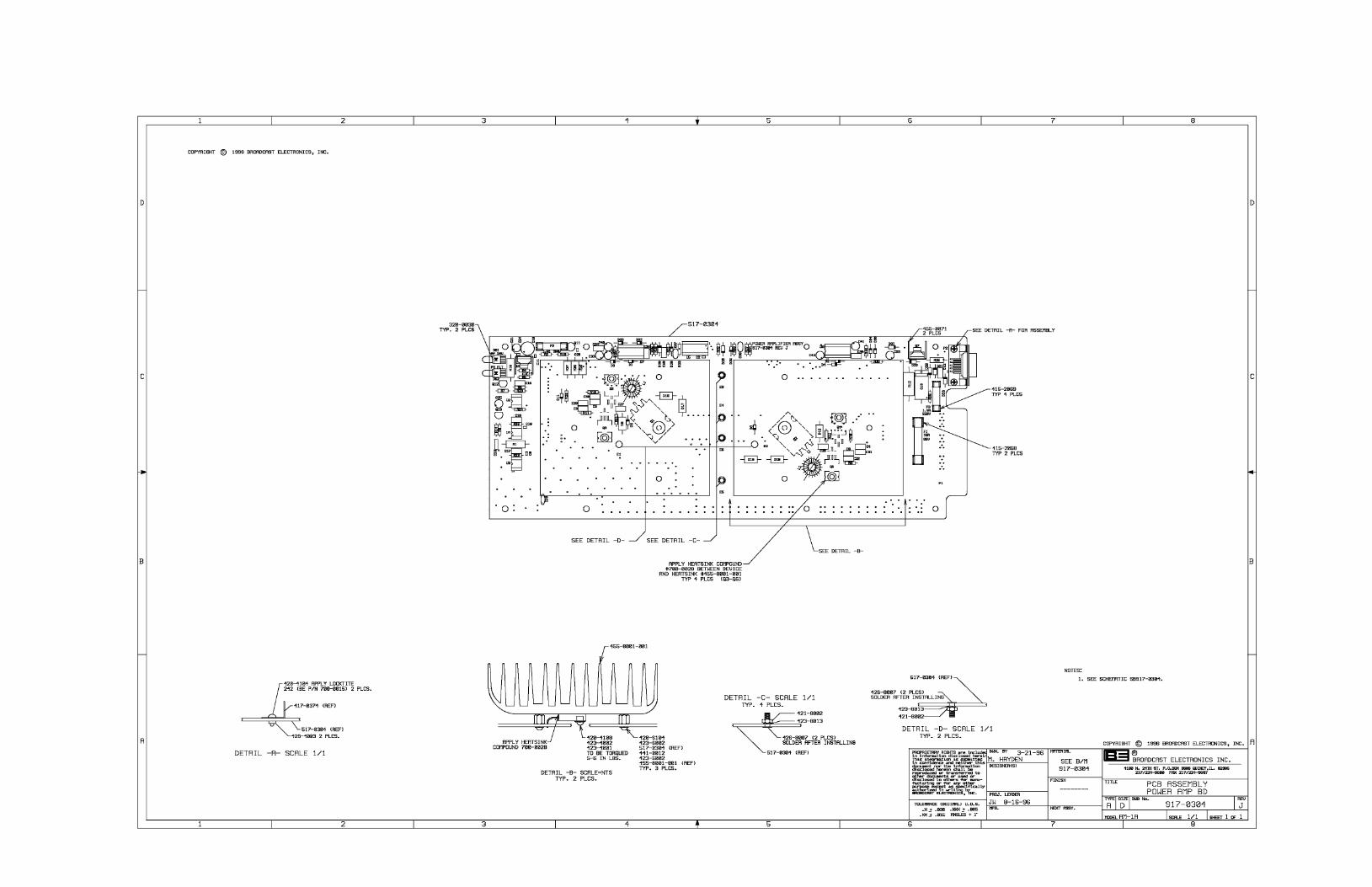

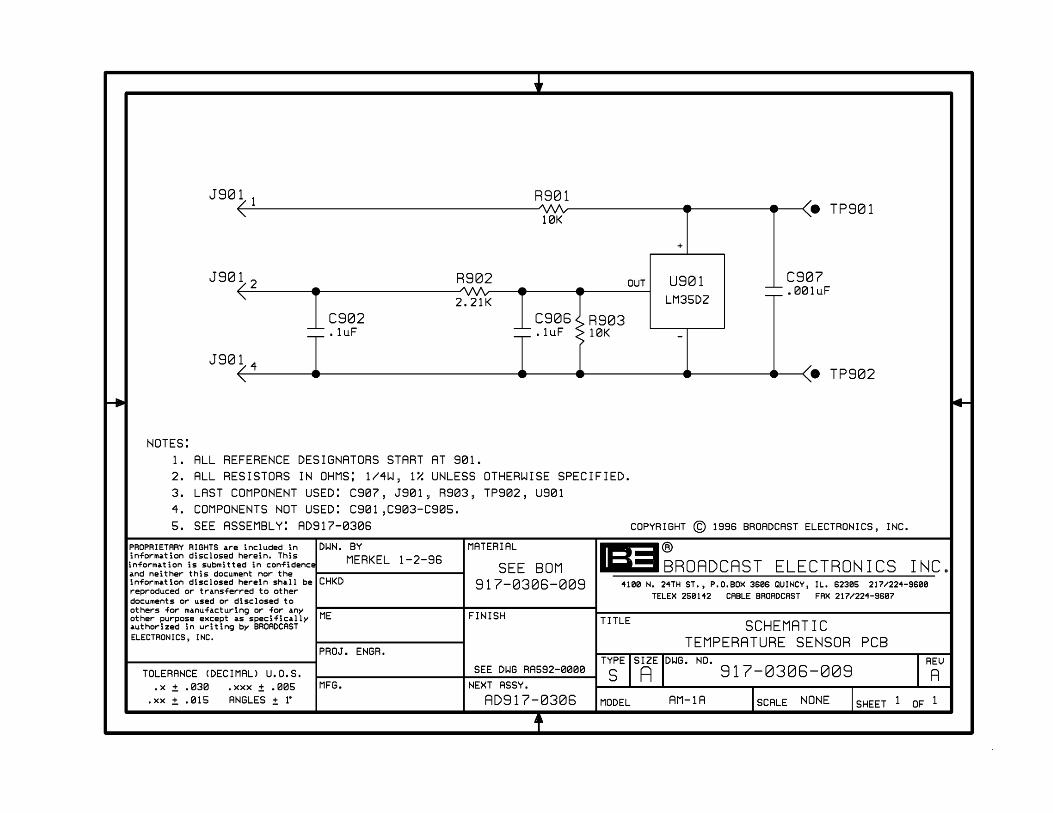
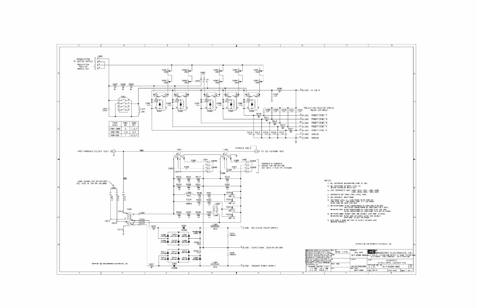
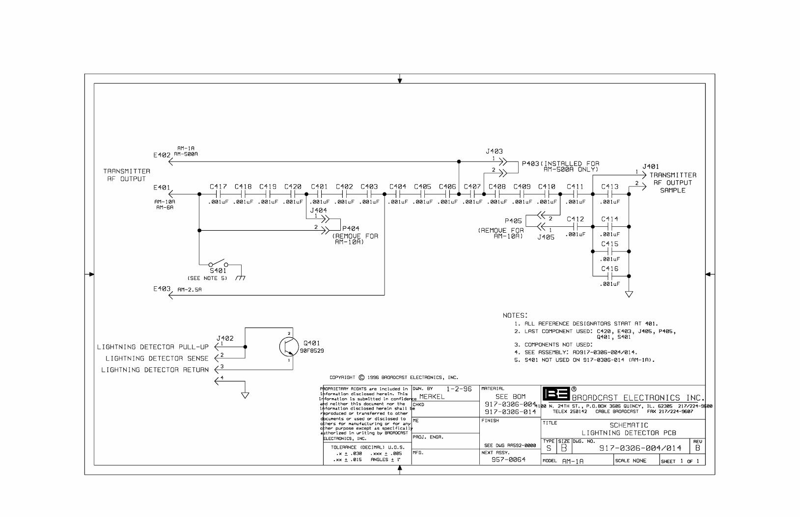


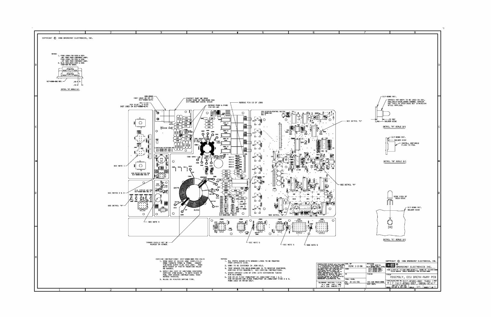
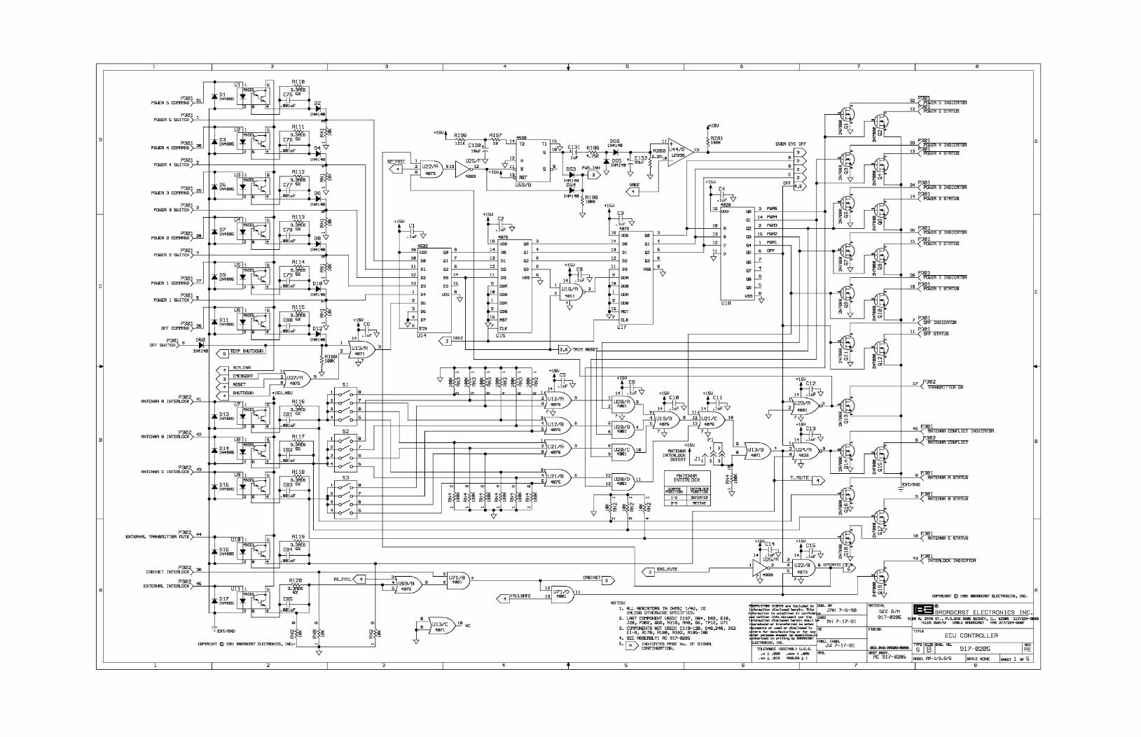
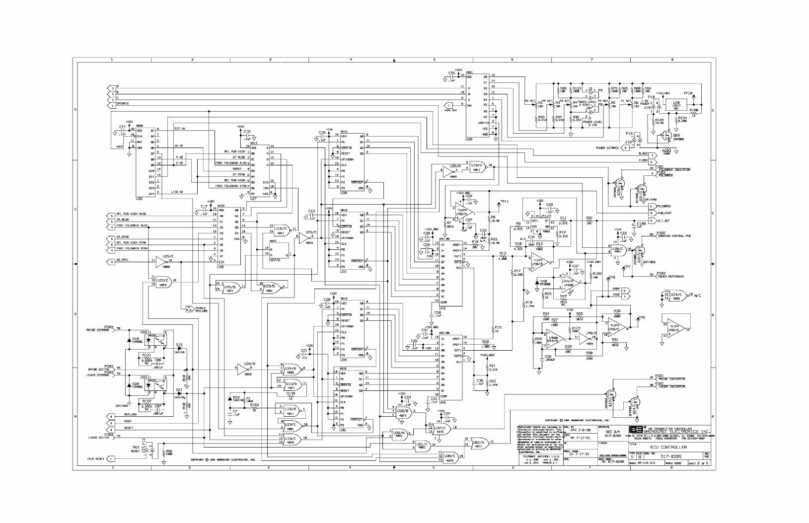


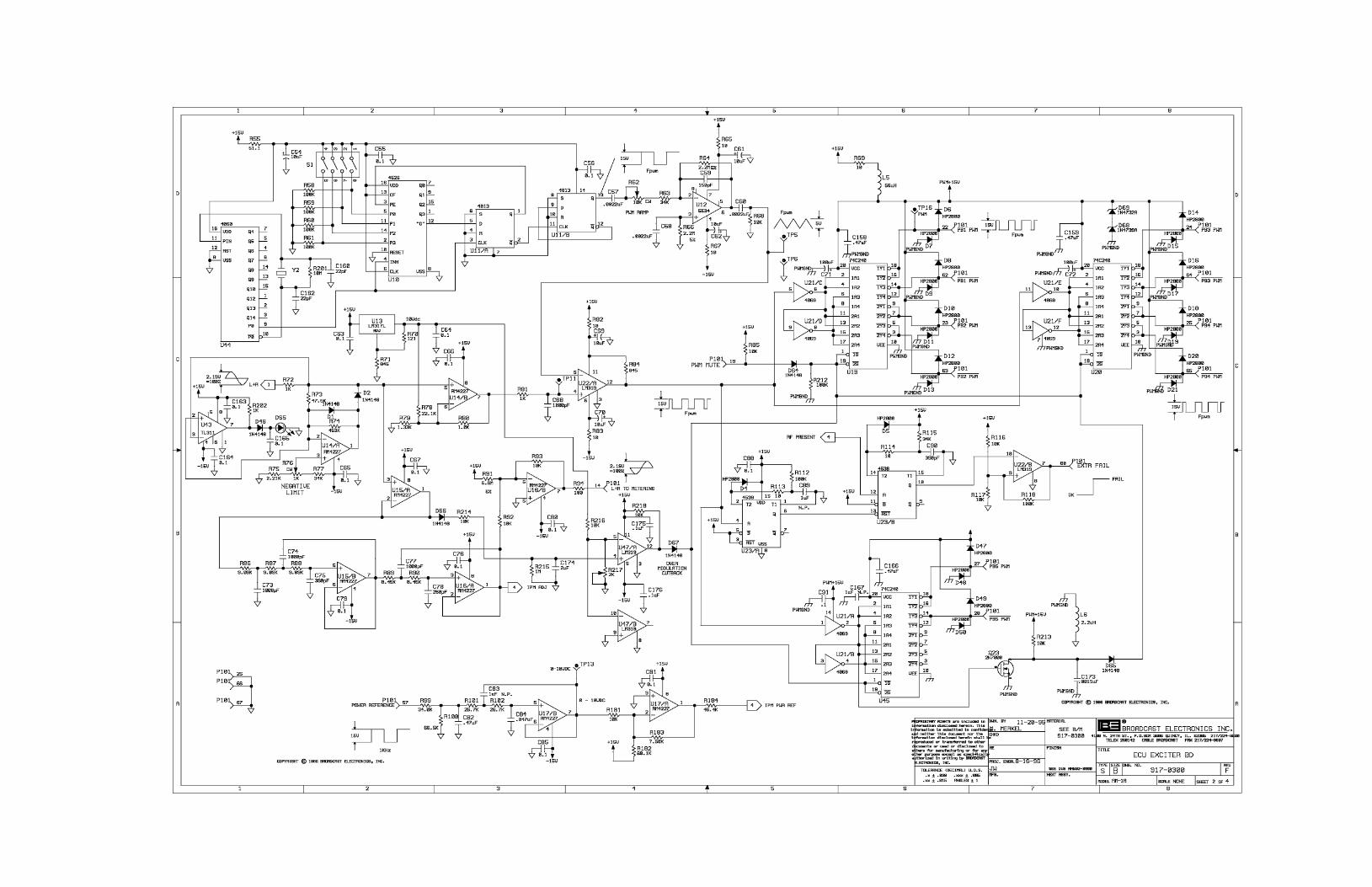
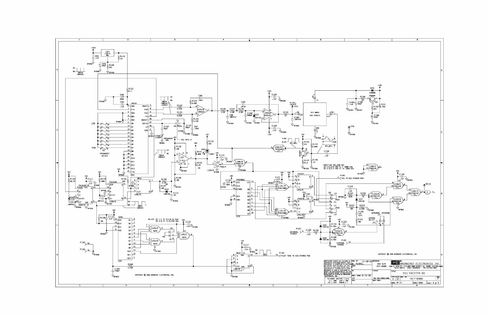
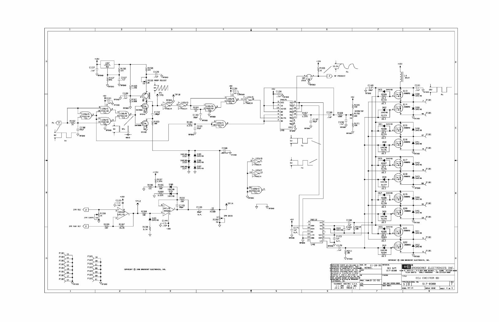
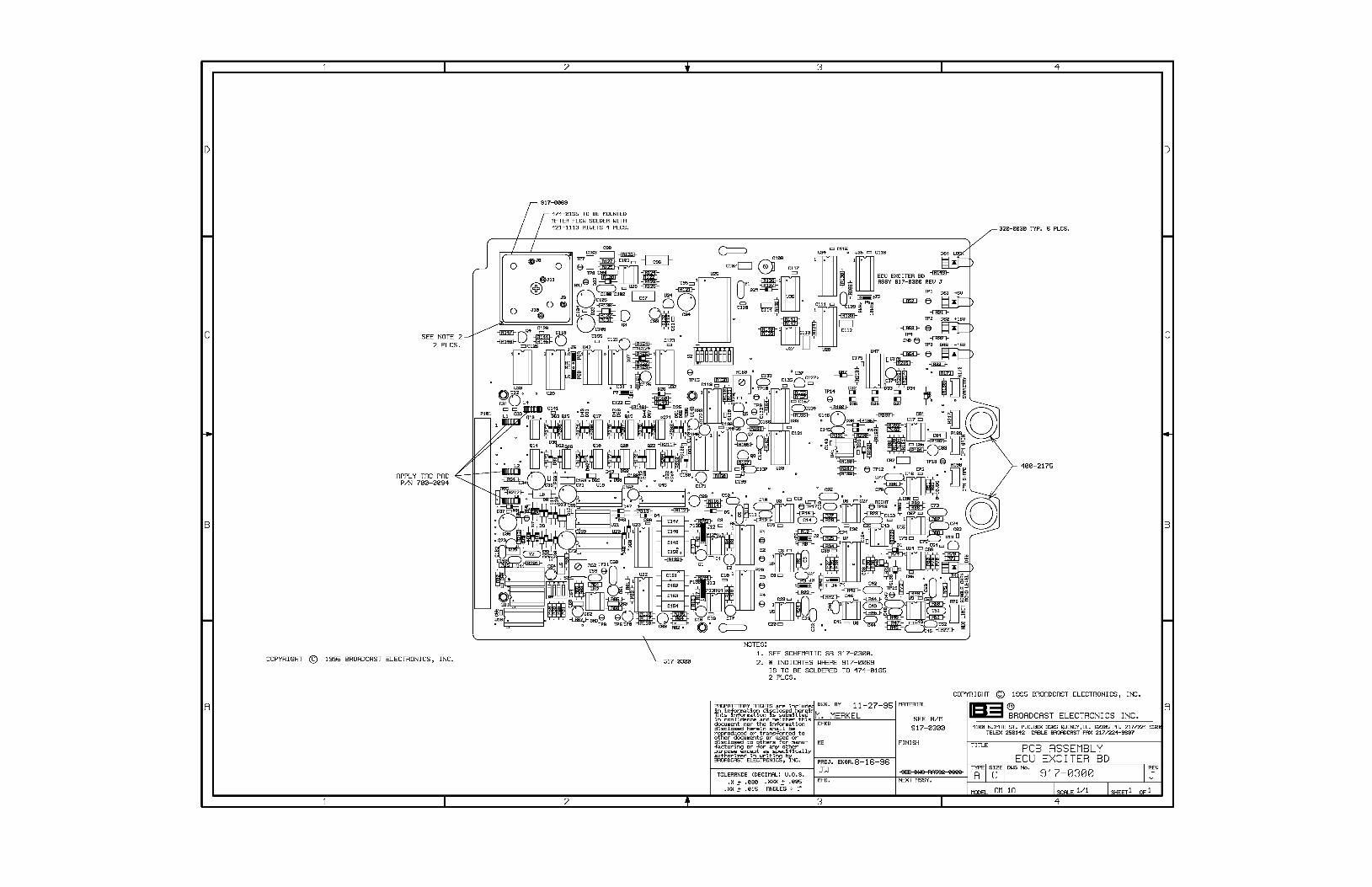
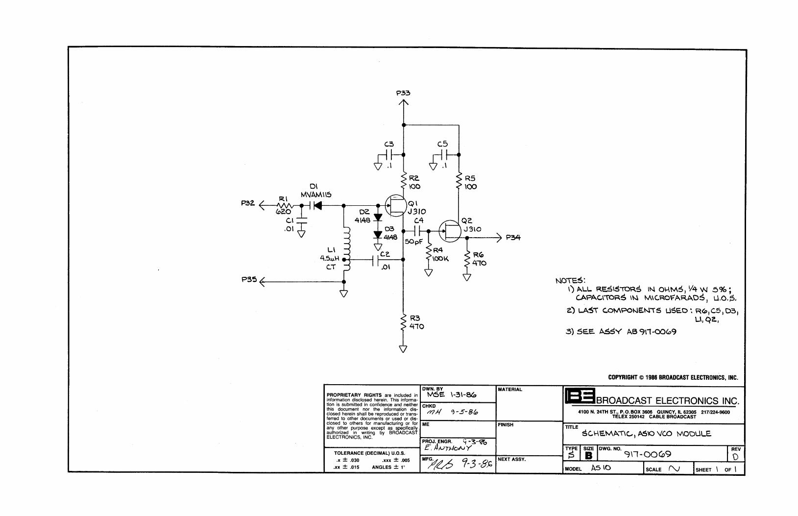
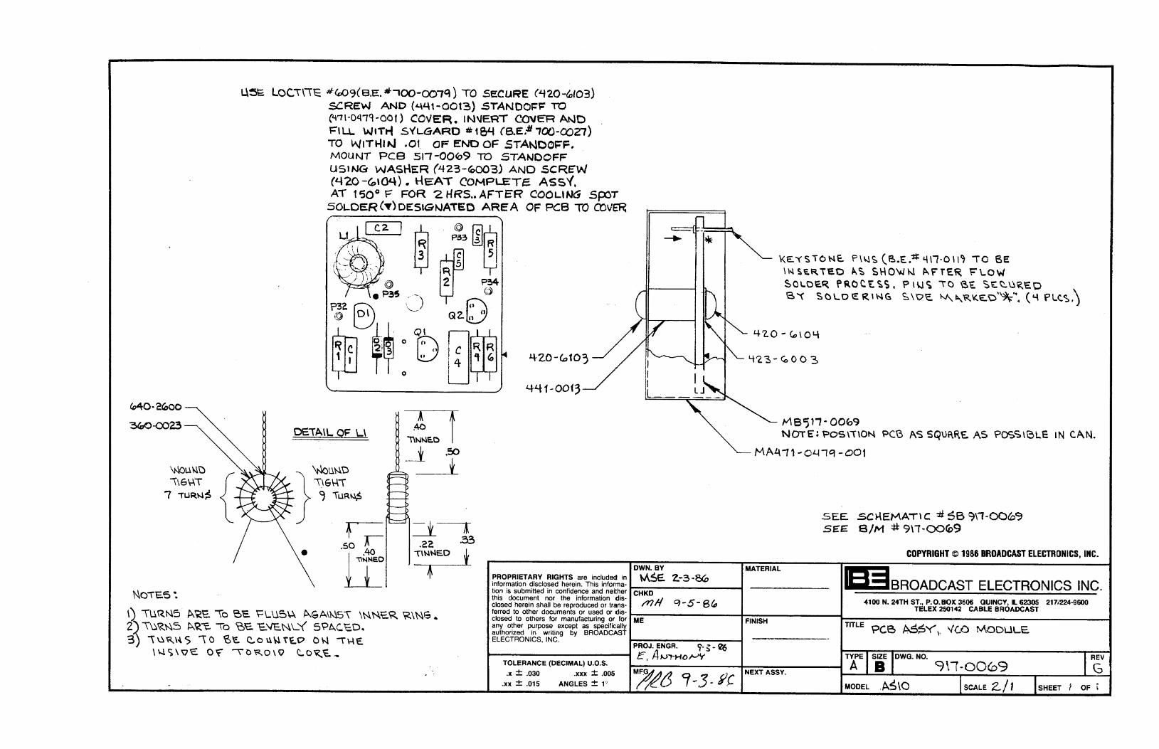
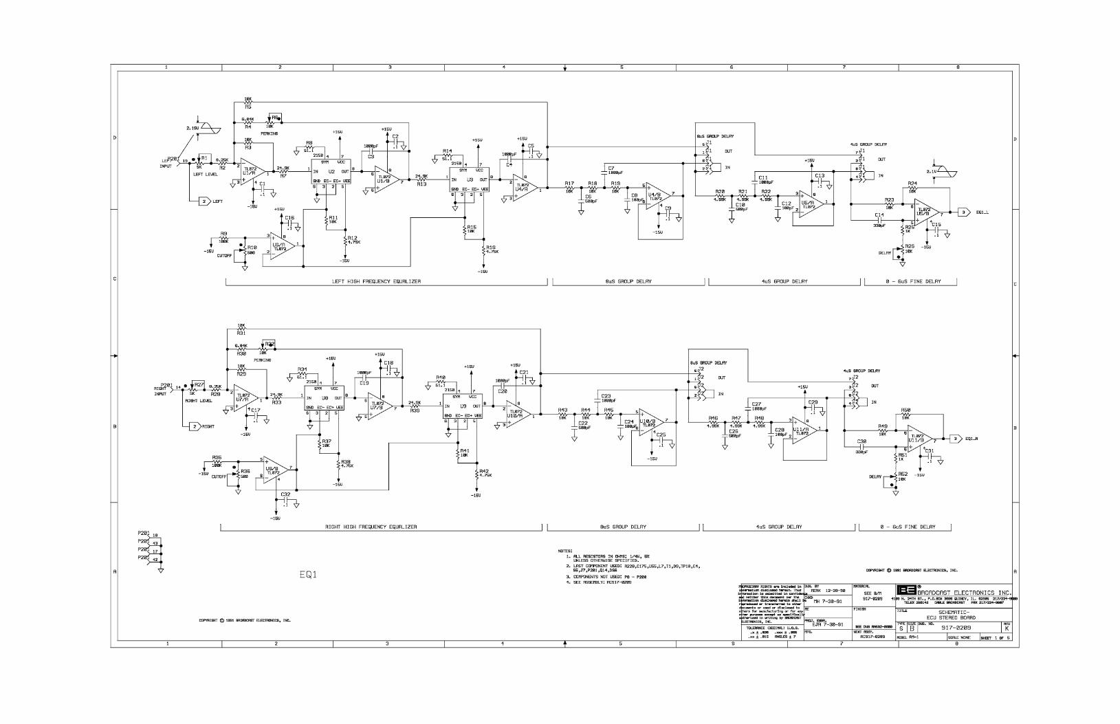
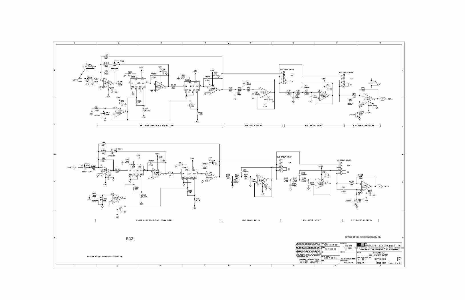

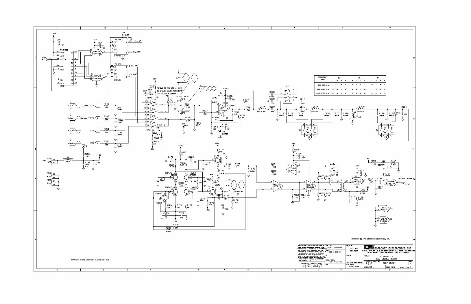
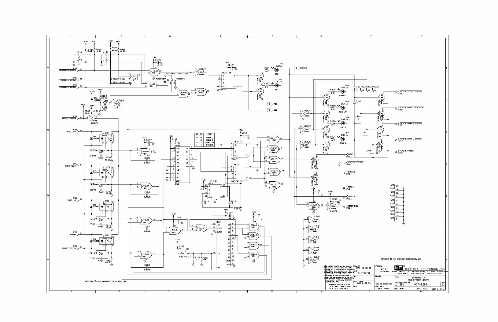
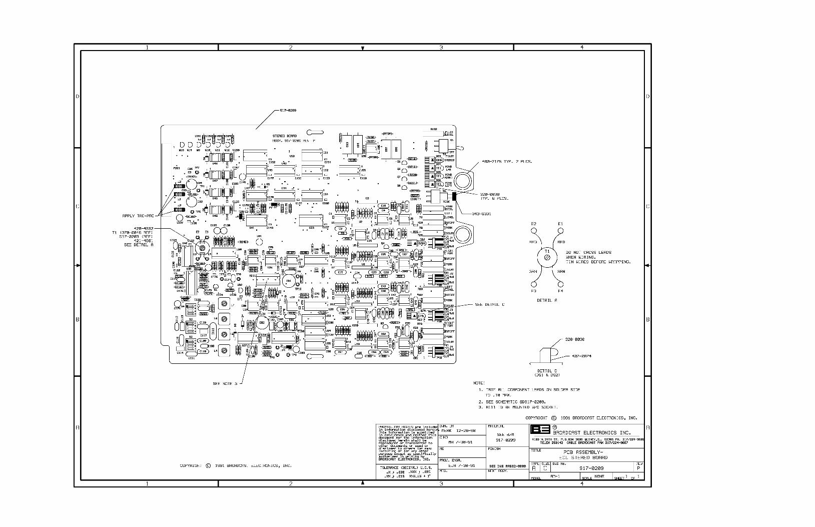
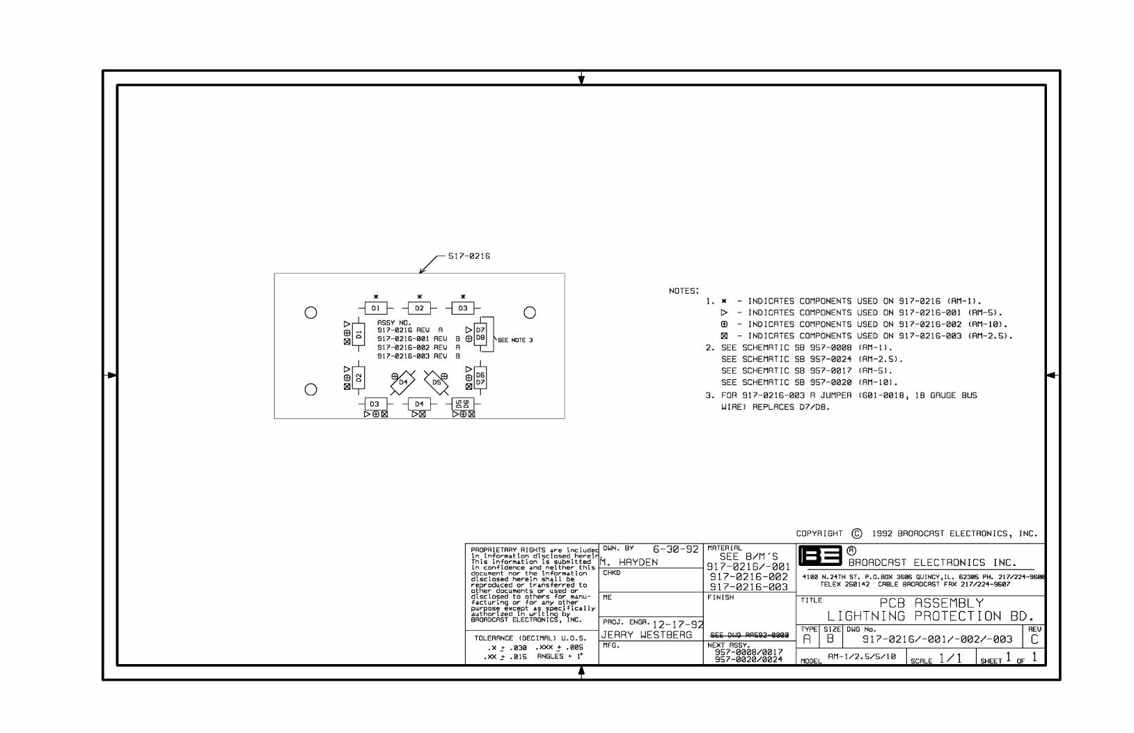
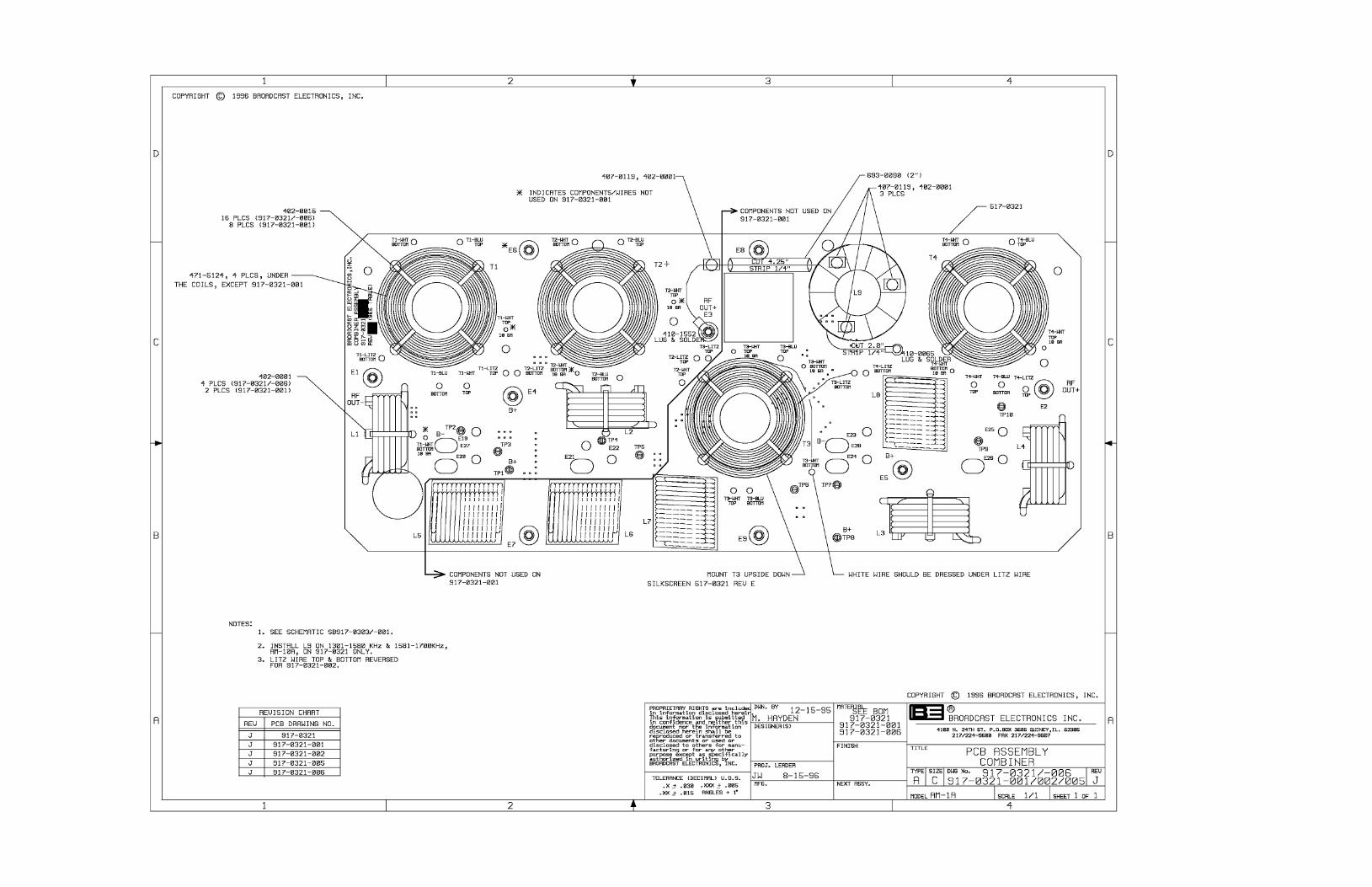
A-1
APPENDIX A
A-1. INTRODUCTION.
A-2. This appendix provides information for the AM matching network. The information
contained in this appendix is presented in the following order.
A. AM matching network.
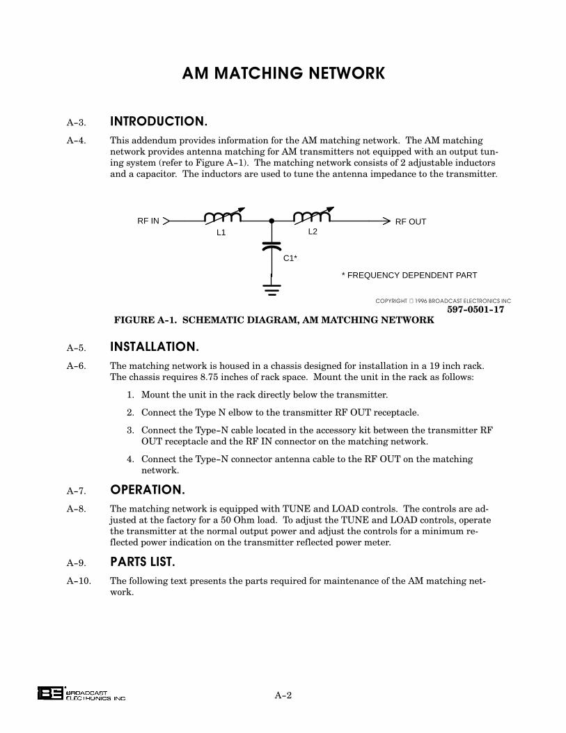
A-2
AM MATCHING NETWORK
A-3. INTRODUCTION.
A-4. This addendum provides information for the AM matching network. The AM matching
network provides antenna matching for AM transmitters not equipped with an output tun�
ing system (refer to Figure A-1). The matching network consists of 2 adjustable inductors
and a capacitor. The inductors are used to tune the antenna impedance to the transmitter.
FIGURE A-1. SCHEMATIC DIAGRAM, AM MATCHING NETWORK597-0501-17
RF INL1 L2
C1*
RF OUT
* FREQUENCY DEPENDENT PART
COPYRIGHT 1996 BROADCAST ELECTRONICS INC
A-5. INSTALLATION.
A-6. The matching network is housed in a chassis designed for installation in a 19 inch rack.
The chassis requires 8.75 inches of rack space. Mount the unit in the rack as follows:
1. Mount the unit in the rack directly below the transmitter.
2. Connect the Type N elbow to the transmitter RF OUT receptacle.
3. Connect the Type-N cable located in the accessory kit between the transmitter RF
OUT receptacle and the RF IN connector on the matching network.
4. Connect the Type-N connector antenna cable to the RF OUT on the matching
network.
A-7. OPERATION.
A-8. The matching network is equipped with TUNE and LOAD controls. The controls are ad�
justed at the factory for a 50 Ohm load. To adjust the TUNE and LOAD controls, operate
the transmitter at the normal output power and adjust the controls for a minimum re�
flected power indication on the transmitter reflected power meter.
A-9. PARTS LIST.
A-10. The following text presents the parts required for maintenance of the AM matching net�
work.

A-3
TABLE A-1. AM MATCHING NETWORK - 907-1000-002
REF. DES. DESCRIPTION PART NO. QTY.
C1 Capacitor, Frequency Dependent, Refer To Frequency Dependent
Parts In The Following Text
L1, L2 Coil, Variable, 16 uH, 20A 360-0088 2
---- Bulkhead Receptacle, Type N 417-0204 2
---- Knob, RB-67-5-M, Black 482-0031 2
---- RF Cable, Type-N Connectors 947-0180 1
---- 90 Degree Elbow, Type-N 417-0105 1
TABLE A-2. FREQUENCY DEPENDENT PARTS - 957-0015-001 THRU -007
REF. DES. DESCRIPTION PART NO. QTY.
FOR ASSEMBLY 957-0015-001
C1 Capacitor, Mica, 3900 pF ±5%, 3kV, 7.5 A, 530 kHz to 650 kHz 044-3923-272 1
FOR ASSEMBLY 957-0015-002
C1 Capacitor, Mica, 3300 pF ±5%, 3kV, 6.8 A, 651 kHz to 770 kHz 044-3323-272 1
FOR ASSEMBLY 957-0015-003
C1 Capacitor, Mica, 2700 pF ±5%, 3kV, 6.8 A, 771 kHz to 920 kHz 044-2723-272 1
FOR ASSEMBLY 957-0015-004
C1 Capacitor, Mica, 2200 pF ±5%, 3kV, 6.2 A, 921 kHz to 1080 kHz 044-2223-272 1
FOR ASSEMBLY 957-0015-005
C1 Capacitor, Mica, 1800 pF ±5%, 5kV, 5.6 A, 1081 kHz to 1300 kHz 044-1823-272 1
FOR ASSEMBLY 957-0015-006
C1 Capacitor, Mica, 1600 pF ±5%, 5kV, 5.6 A, 1301 kHz to 1580 kHz 044-1623-272 1
FOR ASSEMBLY 957-0015-007
C1 Capacitor, Mica, 1300 pF ±5%, 5kV, 5.1 A, 1581 kHz to 1705 kHz 044-1323-272 1


