38
AMD’S “LLANO” FUSION APU Denis Foley , Maurice Steinman, Alex Branover, Greg Smaus, Antonio Asaro, Swamy Punyamurtula, Ljubisa Bajic Hot Chips 23, 19 th August 2011
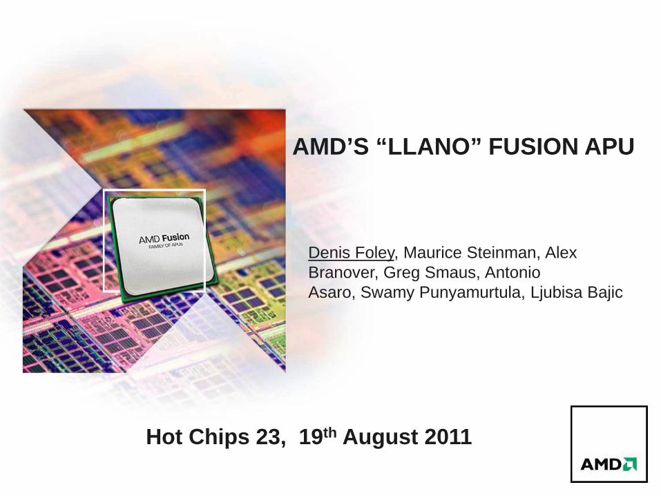
AMD’S “ LLANO ” FUSION APU
Denis Foley, Maurice Steinman, Alex Branover, Greg Smaus, Antonio Asaro, Swamy Punyamurtula, Ljubisa Bajic
Hot Chips 23, 19 th August 2011
2 | LLANO HOT CHIPS | August 19th, 2011
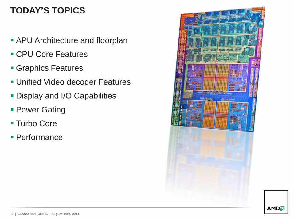
TODAY’S TOPICS
APU Architecture and floorplan
CPU Core Features
Graphics Features
Unified Video decoder Features
Display and I/O Capabilities
Power Gating
Turbo Core
Performance

ARCHITECTURE AND FLOORPLAN

4 | LLANO HOT CHIPS | August 19th, 2011
A-SERIES ARCHITECTURE
• Up to 4 Stars-32nm x86 Cores• 1MB L2 cache/core
• Integrated Northbridge• 2 Chan of DDR3-1866 memory• 24 Lanes of PCIe® Gen2
• x4 UMI (Unified Media Interface)• x4 GPP (General Purpose Ports)• x16 Graphics expansion or display
• 2 x4 Lanes dedicated display• 2 Head Display Controller• UVD (Unified Video Decoder)• 400 AMD Radeon™ Compute Units• GMC (Graphics Memory Controller)• FCL (Fusion Control Link)• RMB (AMD Radeon™ Memory Bus)• 227mm2, 32nm SOI• 1.45BN transistors

5 | LLANO HOT CHIPS | August 19th, 2011
INTERNAL BUS
Fusion Control Link (FCL)
– 128b (each direction) path for IO access to memory
– Variable clock based on throughput (LCLK)
– GPU access to coherent memory space
– CPU access to dedicated GPU framebuffer
AMD Radeon™ Memory Bus (RMB)
– 256b (each direction) for each channel for GMC access to memory
– Runs on Northbridge clock (NCLK)
– Provides full bandwidth path for Graphics access to system memory
– DRAM friendly stream of reads and write
– Bypasses coherency mechanism

6 | LLANO HOT CHIPS | August 19th, 2011
CPU
CPU
CPU
CPU
NB
L2
L2
L2
L2
DDR3UVD
Graphics SIMD Array
Display
Multimedia
I/O
PCIe PCIe
PCIe
DisplayDis
play
PP
L
4 Stars -32nmCPU cores
CPU
CPU
CPU
CPU
Integrated Northbridge
NB
1 MB L2 cacheper core
L2
L2
L2
L2
Dual -channel DDR3
DDR3 Unified Video DecoderUVD
Integrated GPU, Display
ControllerI/O Controllers
Graphics SIMD Array
Display
I/O Controllers
DisplayDis
play
PP
L
Digital display interfaces
PCIe PCIe
PCIe
PCI Express I/O -24 lanes, optional
digital display interfaces

CPU, GPU, UVD AND IO FEATURES
8 | LLANO HOT CHIPS | August 19th, 2011
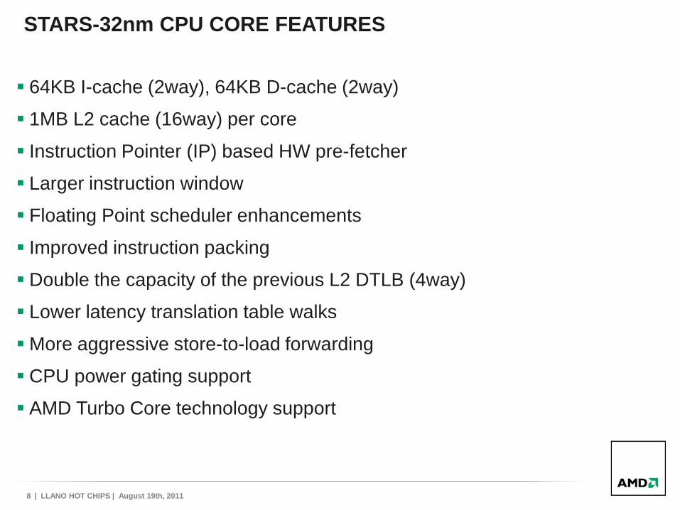
STARS-32nm CPU CORE FEATURES
64KB I-cache (2way), 64KB D-cache (2way)
1MB L2 cache (16way) per core
Instruction Pointer (IP) based HW pre-fetcher
Larger instruction window
Floating Point scheduler enhancements
Improved instruction packing
Double the capacity of the previous L2 DTLB (4way)
Lower latency translation table walks
More aggressive store-to-load forwarding
CPU power gating support
AMD Turbo Core technology support
9 | LLANO HOT CHIPS | August 19th, 2011
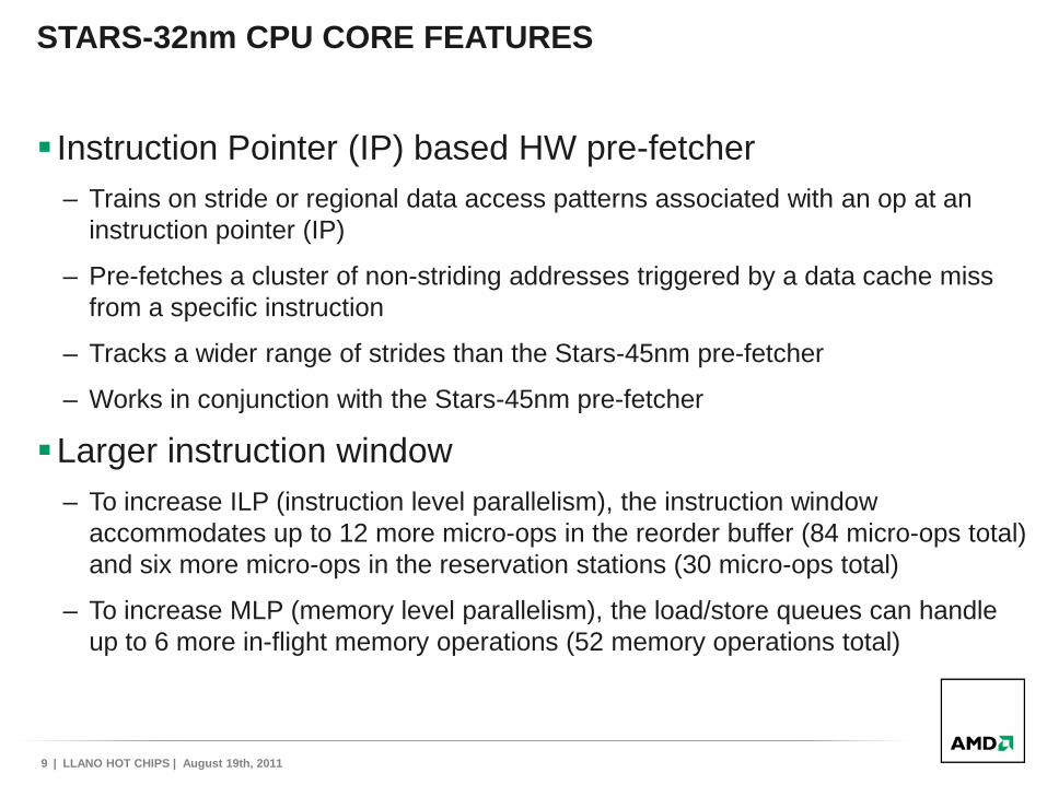
STARS-32nm CPU CORE FEATURES
Instruction Pointer (IP) based HW pre-fetcher– Trains on stride or regional data access patterns associated with an op at an
instruction pointer (IP)
– Pre-fetches a cluster of non-striding addresses triggered by a data cache miss from a specific instruction
– Tracks a wider range of strides than the Stars-45nm pre-fetcher
– Works in conjunction with the Stars-45nm pre-fetcher
Larger instruction window – To increase ILP (instruction level parallelism), the instruction window
accommodates up to 12 more micro-ops in the reorder buffer (84 micro-ops total) and six more micro-ops in the reservation stations (30 micro-ops total)
– To increase MLP (memory level parallelism), the load/store queues can handle up to 6 more in-flight memory operations (52 memory operations total)

10 | LLANO HOT CHIPS | August 19th, 2011
GPU - AMD RADEON™ VLIW-5 CORE
Includes– 4 Stream Cores – 1 Special Functions Stream Core– Branch Unit– General Purpose Registers
4 Stream Cores are capable of – 4 32-bit FP MULADD per clock– 4 24-bit Int MUL or ADD per clock– 2 64-bit FP MUL or ADD per clock– 1 64-bit FP MULADD per clock
Additional special function core– 1 32b-FP MULADD per clock

11 | LLANO HOT CHIPS | August 19th, 2011
GPU - AMD RADEON™ VLIW-5 CORE
Increased IPC
– More flexible dot products
– Co-issue MUL and dependent ADD in a single clock
– Sum of Absolute Differences (SAD)
12x speed-up with native instruction
Used for video encoding, computer vision
Exposed via OpenCL extension
– DirectX 11 bit-level ops
Bit count, insert, extract, etc.
– Fused Multiply-Add
12 | LLANO HOT CHIPS | August 19th, 2011
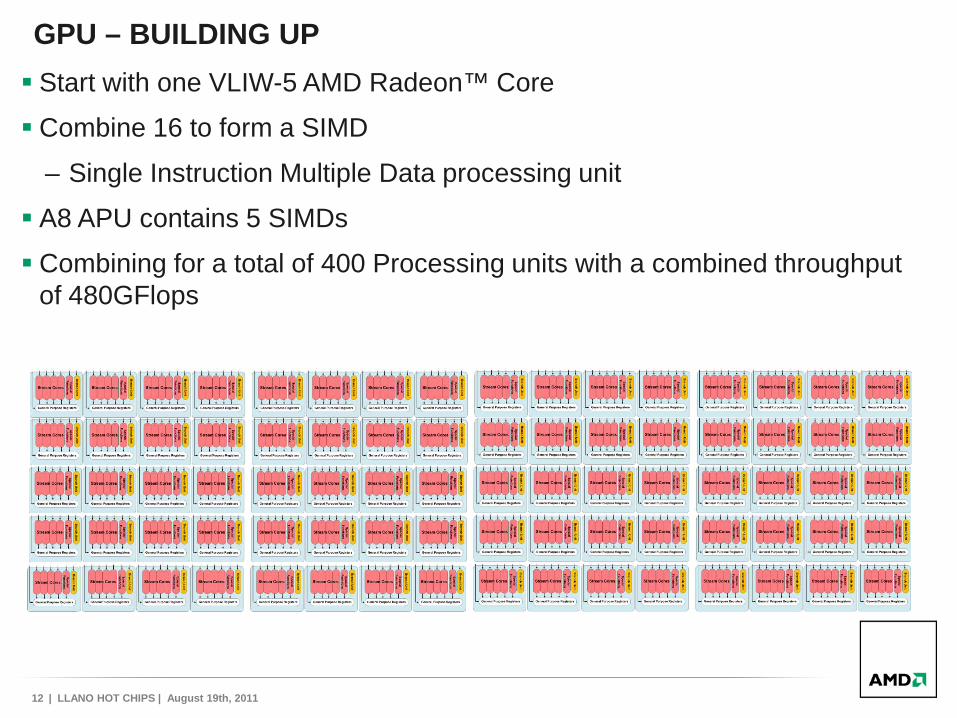
GPU – BUILDING UP
Start with one VLIW-5 AMD Radeon™ Core
Combine 16 to form a SIMD
– Single Instruction Multiple Data processing unit
A8 APU contains 5 SIMDs
Combining for a total of 400 Processing units with a combined throughput of 480GFlops

13 | LLANO HOT CHIPS | August 19th, 2011
GPU BLOCK DIAGRAM
Full DirectX®11 support and features– Including Tessellation unit
– Accessible through Hull & Domain shaders
14 | LLANO HOT CHIPS | August 19th, 2011
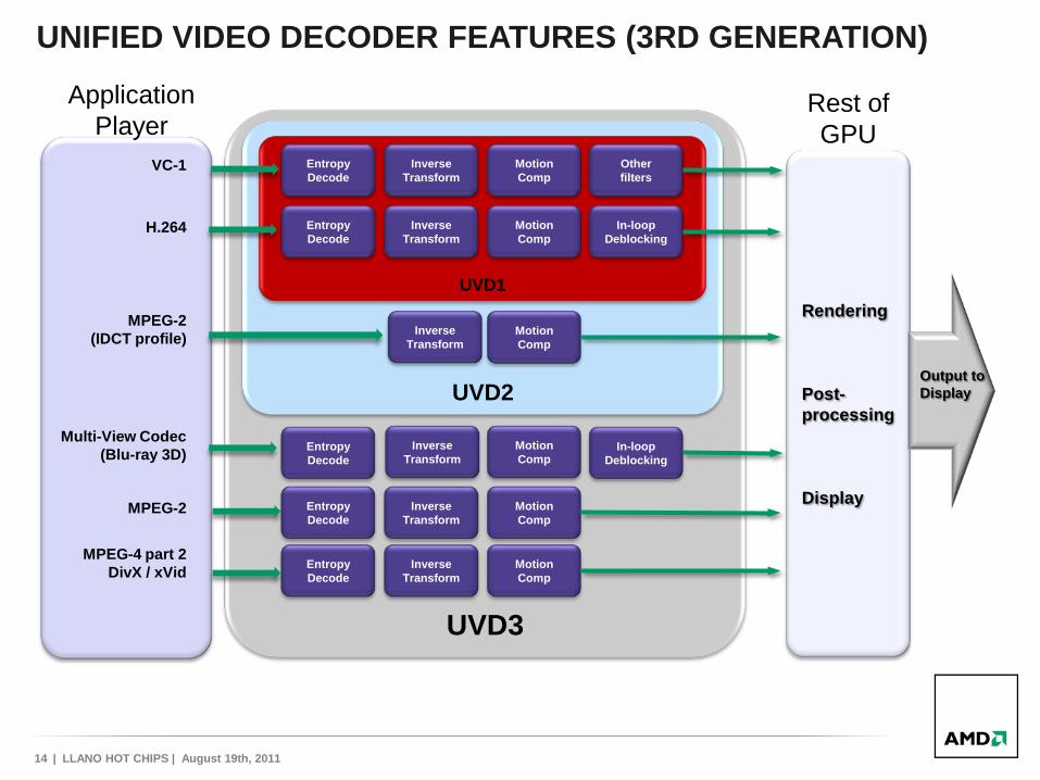
UNIFIED VIDEO DECODER FEATURES (3RD GENERATION)
UVD3
UVD2
UVD1
InverseTransform
MPEG-2(IDCT profile)
H.264
VC-1
EntropyDecode
In-loopDeblocking
EntropyDecode
InverseTransform
Motion Comp
Other filters
InverseTransform
Motion Comp
Motion Comp
MPEG-4 part 2DivX / xVid
EntropyDecode
InverseTransform
Motion Comp
MPEG-2 EntropyDecode
InverseTransform
Motion Comp
EntropyDecode
InverseTransform
Motion Comp
In-loopDeblocking
Multi -View Codec(Blu -ray 3D)
Rendering
Post -processing
Display
Output to Display
Application Player
Rest of GPU
15 | LLANO HOT CHIPS | August 19th, 2011
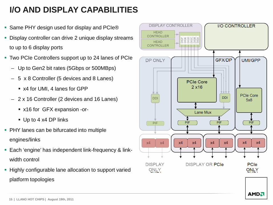
I/O AND DISPLAY CAPABILITIES
Same PHY design used for display and PCIe®
Display controller can drive 2 unique display streams
to up to 6 display ports
Two PCIe Controllers support up to 24 lanes of PCIe
– Up to Gen2 bit rates (5Gbps or 500MBps)
– 5 x 8 Controller (5 devices and 8 Lanes)
x4 for UMI, 4 lanes for GPP
– 2 x 16 Controller (2 devices and 16 Lanes)
x16 for GFX expansion -or-
Up to 4 x4 DP links
PHY lanes can be bifurcated into multiple
engines/links
Each ‘engine’ has independent link-frequency & link-
width control
Highly configurable lane allocation to support varied
platform topologies

POWER GATING
17 | LLANO HOT CHIPS | August 19th, 2011
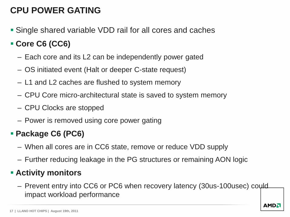
CPU POWER GATING
Single shared variable VDD rail for all cores and caches
Core C6 (CC6)
– Each core and its L2 can be independently power gated
– OS initiated event (Halt or deeper C-state request)
– L1 and L2 caches are flushed to system memory
– CPU Core micro-architectural state is saved to system memory
– CPU Clocks are stopped
– Power is removed using core power gating
Package C6 (PC6)
– When all cores are in CC6 state, remove or reduce VDD supply
– Further reducing leakage in the PG structures or remaining AON logic
Activity monitors
– Prevent entry into CC6 or PC6 when recovery latency (30us-100usec) could impact workload performance
18 | LLANO HOT CHIPS | August 19th, 2011
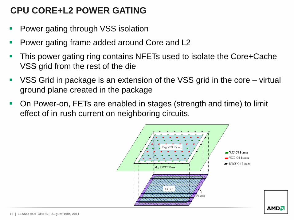
CPU CORE+L2 POWER GATING
Power gating through VSS isolation
Power gating frame added around Core and L2
This power gating ring contains NFETs used to isolate the Core+CacheVSS grid from the rest of the die
VSS Grid in package is an extension of the VSS grid in the core – virtual ground plane created in the package
On Power-on, FETs are enabled in stages (strength and time) to limit effect of in-rush current on neighboring circuits.
19 | LLANO HOT CHIPS | August 19th, 2011
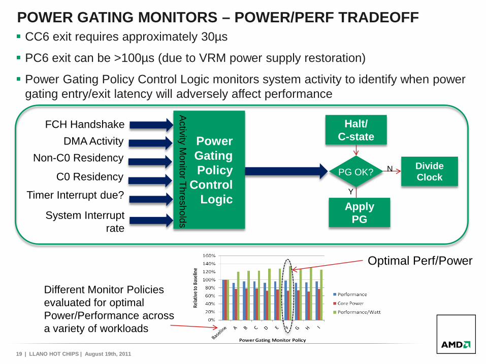
POWER GATING MONITORS – POWER/PERF TRADEOFF CC6 exit requires approximately 30µs
PC6 exit can be >100µs (due to VRM power supply restoration)
Power Gating Policy Control Logic monitors system activity to identify when power gating entry/exit latency will adversely affect performance
Power Gating Policy
Control Logic
System Interrupt rate
DMA Activity
Non-C0 Residency
C0 Residency
FCH Handshake
Timer Interrupt due?
Halt/ C-state
Apply PG
Divide Clock
Y
N
Activity M
onitor Thresholds
PG OK?
Different Monitor Policiesevaluated for optimal Power/Performance acrossa variety of workloads
Optimal Perf/Power
20 | LLANO HOT CHIPS | August 19th, 2011
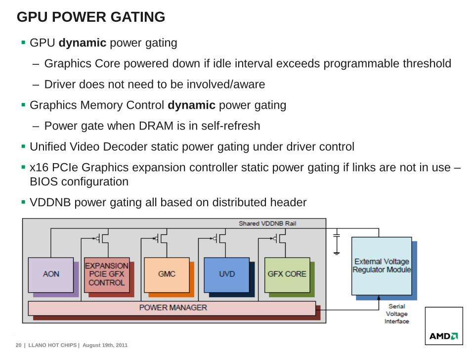
GPU POWER GATING
GPU dynamic power gating
– Graphics Core powered down if idle interval exceeds programmable threshold
– Driver does not need to be involved/aware
Graphics Memory Control dynamic power gating
– Power gate when DRAM is in self-refresh
Unified Video Decoder static power gating under driver control
x16 PCIe Graphics expansion controller static power gating if links are not in use –BIOS configuration
VDDNB power gating all based on distributed header

21 | LLANO HOT CHIPS | August 19th, 2011
UVD AND GRAPHICS COMPUTE COMPLEX POWER GATED (MERIDIAN PHOTON RECOMBINATION)
EVERYTHING ON GRAPHICS GATED
Leakage only, No clocks running. Blue is ambient
UVD GATED
AMD TURBO CORE TECHNOLOGY

23 | LLANO HOT CHIPS | August 19th, 2011
•Power and performance varies a lot by workload
•Power estimated by digital tracking of the APU application activity
•Higher frequency is used when power limit allows for better APU performance delivered within the same Power envelope
•Deterministic performance gains
•Power budget can be dynamically allocated to different Compute Units (in CPU and GPU)
•Over-TDC (Thermal Design Current) protection
AMD TURBO CORE TECHNOLOGY
Measured Dynamic Power
0%
20%
40%
60%
80%
100%
120%
Max
Pow
er12
8H
LTN
OP
Wup
wis
eSi
mM
grid
Appl
uM
esa
Gal
gel
Art
Equa
keFa
cere
cAm
mp
Luca
sFm
a3d
Sixt
rack
Apsi
Gzi
pVp
rG
cc Mcf
Cra
ftyPa
rser
Eon
Perlb
mk
Power Headroom to be exploited
Compliant with ACPI P-state Request/Policy User Policy
24 | LLANO HOT CHIPS | August 19th, 2011
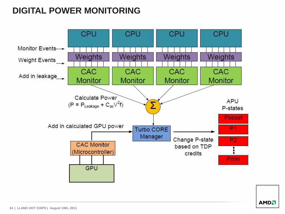
DIGITAL POWER MONITORING
25 | LLANO HOT CHIPS | August 19th, 2011
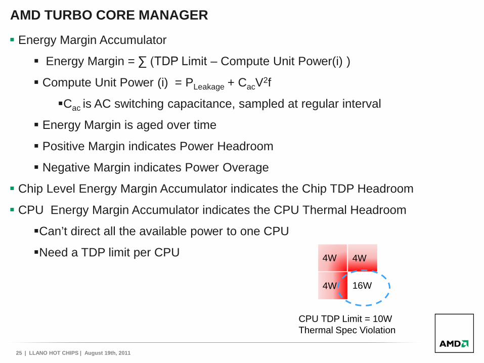
AMD TURBO CORE MANAGER
Energy Margin Accumulator
Energy Margin = ∑ (TDP Limit – Compute Unit Power(i) )
Compute Unit Power (i) = PLeakage + CacV2f
Cac is AC switching capacitance, sampled at regular interval
Energy Margin is aged over time
Positive Margin indicates Power Headroom
Negative Margin indicates Power Overage
Chip Level Energy Margin Accumulator indicates the Chip TDP Headroom
CPU Energy Margin Accumulator indicates the CPU Thermal Headroom
Can’t direct all the available power to one CPU
Need a TDP limit per CPU 4W 4W
4W 16W
CPU TDP Limit = 10WThermal Spec Violation
26 | LLANO HOT CHIPS | August 19th, 2011
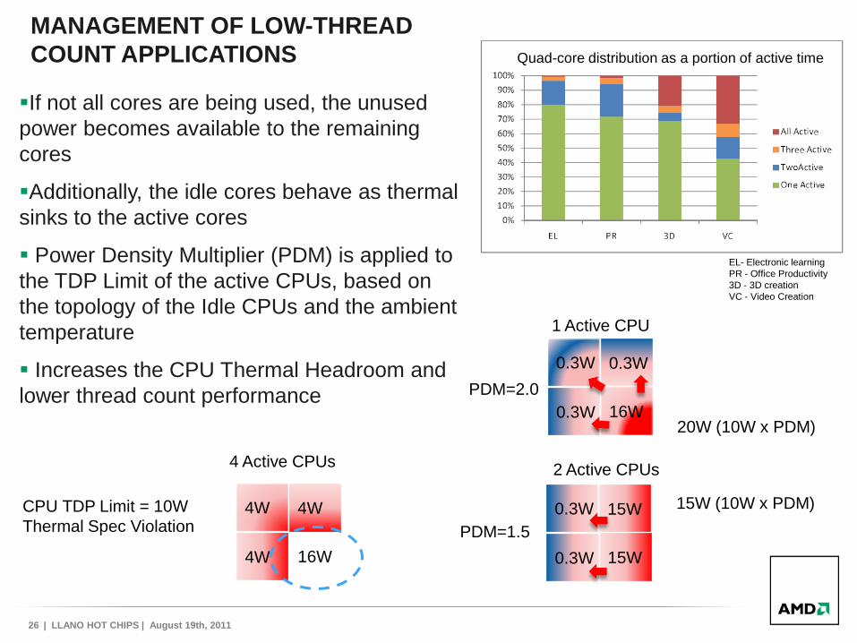
MANAGEMENT OF LOW-THREAD COUNT APPLICATIONS
If not all cores are being used, the unused power becomes available to the remaining cores
Additionally, the idle cores behave as thermal sinks to the active cores
Power Density Multiplier (PDM) is applied to the TDP Limit of the active CPUs, based on the topology of the Idle CPUs and the ambient temperature
Increases the CPU Thermal Headroom and lower thread count performance
4W 4W
4W 16W
CPU TDP Limit = 10WThermal Spec Violation
4 Active CPUs
0.3W 0.3W
0.3W 16W20W (10W x PDM)
0.3W 15W
0.3W 15W
15W (10W x PDM)
PDM=2.0
PDM=1.5
1 Active CPU
2 Active CPUs
EL- Electronic learningPR - Office Productivity3D - 3D creationVC - Video Creation
Quad-core distribution as a portion of active time
27 | LLANO HOT CHIPS | August 19th, 2011
IDLE
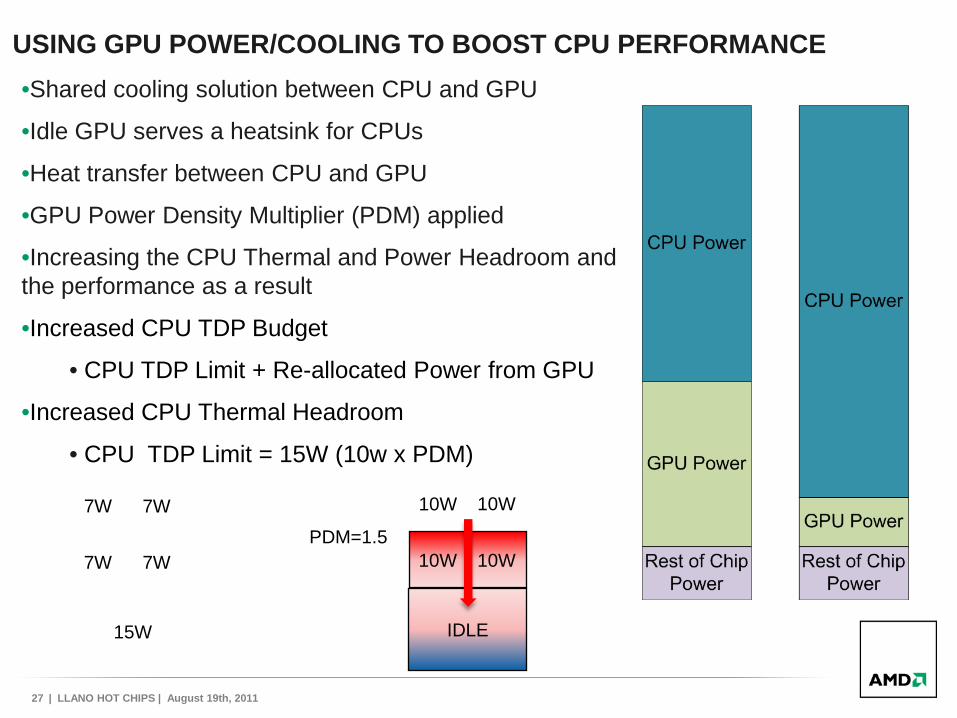
USING GPU POWER/COOLING TO BOOST CPU PERFORMANCE
•Shared cooling solution between CPU and GPU
•Idle GPU serves a heatsink for CPUs
•Heat transfer between CPU and GPU
•GPU Power Density Multiplier (PDM) applied
•Increasing the CPU Thermal and Power Headroom and the performance as a result
•Increased CPU TDP Budget
• CPU TDP Limit + Re-allocated Power from GPU
•Increased CPU Thermal Headroom
• CPU TDP Limit = 15W (10w x PDM)
7W
PDM=1.5
7W
7W 7W
15W
10W 10W
10W 10W
28 | LLANO HOT CHIPS | August 19th, 2011
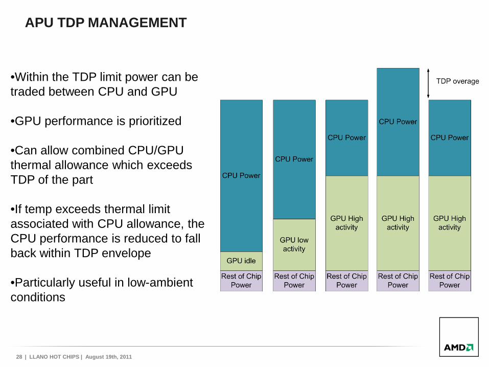
APU TDP MANAGEMENT Load-balancing Open CL(CPU Max Power + OCCT8)
•Within the TDP limit power can be traded between CPU and GPU
•GPU performance is prioritized
•Can allow combined CPU/GPU thermal allowance which exceeds TDP of the part
•If temp exceeds thermal limit associated with CPU allowance, the CPU performance is reduced to fall back within TDP envelope
•Particularly useful in low-ambient conditions
PERFORMANCE
30 | LLANO HOT CHIPS | August 19th, 2011
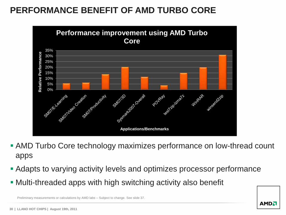
PERFORMANCE BENEFIT OF AMD TURBO CORE
AMD Turbo Core technology maximizes performance on low-thread count apps
Adapts to varying activity levels and optimizes processor performance
Multi-threaded apps with high switching activity also benefit
0%5%
10%15%20%25%30%35%
Rel
ativ
e P
erfo
rman
ce
Applications/Benchmarks
Performance improvement using AMD Turbo Core
Preliminary measurements or calculations by AMD labs – Subject to change. See slide 37.

31 | LLANO HOT CHIPS | August 19th, 2011
AMD A8 APU VS. PHENOM II X4 PROCESSOR PERFORMANCE
A8 benefits from significant IPC features:
– Advanced pre-fetchers
– Bigger instruction window support
Preliminary measurements or calculations by AMD labs – Subject to change. See slide 37.
94%96%98%
100%102%104%106%108%110%112%
Rel
ativ
e P
erfo
rman
ce
Phe
nom
II x
4 =
1.0
Llano vs Phenom II x4 mobile(Performance at same core frequency )
32 | LLANO HOT CHIPS | August 19th, 2011
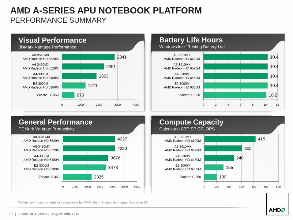
General PerformancePCMark Vantage Productivity
Compute CapacityCalculated CTP SP GFLOPS
Visual Performance3DMark Vantage Performance
AMD A-SERIES APU NOTEBOOK PLATFORM PERFORMANCE SUMMARY
670
1271
1863
2261
2841
0 1000 2000 3000 4000
"Zacate" E-350
E2-3000M AMD Radeon HD 6380M
A4-3300M AMD Radeon HD 6480M
A6-3410MX AMD Radeon HD 6520M
A8-3510MX AMD Radeon HD 6620M
Battery Life HoursWindows Idle “Resting Battery Life”
Preliminary measurements or calculations by AMD labs – Subject to change. See slide 37.
2325
3478
3676
4220
4227
0 1000 2000 3000 4000 5000 6000
"Zacate" E-350
E2-3000M AMD Radeon HD 6380M
A4-3300M AMD Radeon HD 6480M
A6-3410MX AMD Radeon HD 6520M
A8-3510MX AMD Radeon HD 6620M
10.2
10.4
10.4
10.4
10.4
0 2 4 6 8 10 12
"Zacate" E-350
E2-3000M AMD Radeon HD 6380M
A4-3300M AMD Radeon HD 6480M
A6-3410MX AMD Radeon HD 6520M
A8-3510MX AMD Radeon HD 6620M
100
155
240
305
415
0 100 200 300 400 500 600
"Zacate" E-350
E2-3000M AMD Radeon HD 6380M
A4-3300M AMD Radeon HD 6480M
A6-3410MX AMD Radeon HD 6520M
A8-3510MX AMD Radeon HD 6620M

33 | LLANO HOT CHIPS | August 19th, 2011
THANK YOU!

34 | LLANO HOT CHIPS | August 19th, 2011
BACKUP & GLOSSARY

35 | LLANO HOT CHIPS | August 19th, 2011
GLOSSARY
A8, A6, A4 – Names for the various members of the A-series family of products
ADD – Add instruction
AON – Always On – refers to logic that is not power gated
APU- Application Processing Unit- term used for combined x86/MM/GPU chip:
A-Series : Family of fusion APUs including A8, A6, A4
CAC – Switching capacitance
CC6 – Core C-state where the core is powered off
C-state – ACPI defined operating mode of a processor
C0 – State in which Core is operational
DDI – Digital Display Interface
DP – Display Port – Digital Display interface standard
FCH – Fusion Controller Hub – sometimes referred to as a Southbridge
FCL – Fusion Control link – internal data bus for IO and GPU access to memory
GFX – Graphics Core or 3D core
GMC – Graphics memory controller – hub and arbiter servicing graphics and multimedia client requests to memory
GPP – General Purpose Port
GPU – Graphics processing unit
ILP – Instruction level parallelism
IPC – Instructions per cycle – a measure of the number of instructions retired per clock period
MAD – Mul/Add instruction
MLP – Memory level parallelism
MM – Multimedia
MUL – Multiply instruction
PC6 – Package C-state where all cores on the die are powered off
PDM – Power density multiplier
PG – Power gating
PIF – Phy Interface
P-states – ACPI defined power states
RMB – AMD Radeon™ Memory bus – high bandwidth non-coherent access path from GMC to system memory
SAD – Sum of absolute differences
SIMD – Single instruction multiple data
Stars – AMD’s x86 CPU.
TDP – Thermal Design power – a measure of a design infrastructure’s ability to cool a device
Turbo Core – AMD boost mechanism
UMI – Unified Media Interface – connection from APU to Fusion Control Hub
UVD – Unified Video Decoder
VDD – Core power supply rail
VDDNB – Graphics and Northbridge power supply rail
VLIW – Very long Instruction Word
VRM – Voltage regulator module
VSS – Common ground on the die

36 | LLANO HOT CHIPS | August 19th, 2011
ADDITIONAL INFORMATION FOR HANDOUTS
Slide 6 is animated and shows the various blocks on the floorplan. The final slide has all the detail
Slides 10 and 11 introduce the basic building block of the GPU – the AMD Radeon™ Core
Slide 12 is animated and shows the progression from a single AMD Radeon™ Core to form a SIMD and then to form the complete GPU processing complex
Slide 13 shows how the GPU processing complex fits in the context of the graphics engine
37 | LLANO HOT CHIPS | August 19th, 2011
NOTEBOOK SYSTEM CONFIGURATIONS
AMD System Configurations :The 2010 VISION System consisted of the AMD Athlon™ II Dual-Core Processor N350 with ATI Mobility AMD Radeon™ HD 4250 Graphics 2x2GB DDR3-1333 system memory, 14” 1366x768x32 – LED Backlight Windows 7 Home Premium 64-bit
The 2011 AMD VISION-based notebook consisted of an AMD Dual-Core Processor E-350, 2x2GB DDR3-1333 system memory, on die AMD Radeon™ HD 6310 Graphics with 14” 1366x768x32 – LED Backlight Windows 7 Home Premium 64-bit
2011 Mainstream Notebook Platform Reference Design with AMD Dual-Core Accelerated Processor A4-3300M and on die AMD Radeon™ HD 6480M Graphics; 2x2GB DDR3-1333,160GB HD, Windows 7 Ultimate (8.65 beta driver)
2011 Mainstream Notebook Platform Reference Design with AMD Quad-Core Accelerated Processor A6-3410MX and on die AMD Radeon™ HD 6520M Graphics, 2x2GB DDR3-1333, 160GB HD, Windows 7 Ultimate (8.65 beta driver)
2011 Mainstream Notebook Platform Reference Design with AMD Quad-Core Accelerated Processor A8-3510MX and on die AMD Radeon™ HD 6620M Graphics, 2x3GB DDR3-1333 160GB HD, Windows 7 Ultimate (8.65 beta driver)
AMD TurboCore :2011 Mainstream Notebook Platform Reference Design with AMD Quad-Core Accelerated Processor A8-3510MX and on die AMD Radeon™ HD 6620M Graphics, 2x3GB DDR3-1333 160GB HD, Windows 7 Ultimate (8.65 beta driver)
IPC Comparison :2011 Mainstream Notebook Platform Reference Design with AMD Quad-Core Accelerated Processor A8-3530MX and on die AMD Radeon™ HD 6620M Graphics, 2x2GB DDR3-1333 160GB HD, Windows 7 Ultimate (8.65 beta driver) Turbo-core turned OFF
2010 Mainstream Notebook Platform reference Design with AMD Quad-core Phenom II X920 (clocked at 1.9Ghz CPU freq) and iGPU ATI Mobility Radeon HD 4200 series Graphics, 2x2GB DDR3-1333, Windows 7 ultimate (8.65 Beta driver)

38 | LLANO HOT CHIPS | August 19th, 2011
Disclaimer
The information presented in this document is for informational purposes only and may contain technical inaccuracies, omissions and typographical errors.
The information contained herein is subject to change and may be rendered inaccurate for many reasons, including but not limited to product and roadmap changes, component and motherboard version changes, new model and/or product releases, product differences between differing manufacturers, software changes, BIOS flashes, firmware upgrades, or the like. AMD assumes no obligation to update or otherwise correct or revise this information. However, AMD reserves the right torevise this information and to make changes from time to time to the content hereof without obligation of AMD to notify any person of such revisions or changes.
AMD makes no representations or warranties with respect to the contents hereof and assumes no responsibility for any inaccuracies, errors or omissions that appear in this information.
AMD specifically disclaims any implied warranties of merchantability or fitness for any particular purpose. In no event will AMDbe liable to any person for any direct, indirect, special or other consequential damages arising from the use of any informationcontained herein, even if AMD is expressly advised of the possibility of such damages.
Trademark Attribution
AMD, the AMD Arrow logo, AMD Athlon, AMD Phenom, AMD Turion, AMD Radeon, and combinations thereof are trademarks of Advanced Micro Devices, Inc. in the United States and/or other jurisdictions. Microsoft, Windows and DirectX are registered trademarks of Microsoft Corporation in the United States and/or other jurisdictions. PCIe is a registered trademark of PCI-SIG. Other names used in this presentation are for identification purposes only and may be trademarks of their respective owners.
©2011 Advanced Micro Devices, Inc. All rights reserved.


