Page 1
American Journal of Engineering Education – June 2015 Volume 6, Number 1
Copyright by author(s); CC-BY 11 The Clute Institute
A Solder Based Self Assembly Project In
An Introductory IC Fabrication Course Madhav Rao, International Institute of Information Technology, India
John C Lusth, University of Alabama, USA
Susan L Burkett, University of Alabama, USA
ABSTRACT
Integrated circuit (IC) fabrication principles is an elective course in a senior undergraduate and
early graduate student’s curriculum. Over the years, the semiconductor industry relies heavily on
students with developed expertise in the area of fabrication techniques, learned in an IC
fabrication theory and laboratory course. The theory course gives importance to the physics of
manufacturing techniques and is often attached to a subsequent semester laboratory curriculum.
The pre-requisite requirement of the theory component for a laboratory course requires students
to enroll for two courses in separate semesters and is not an option for all students. Hence, an
innovative student project is intended in the theory curriculum to give hands-on experience on the
processes. The IC fabrication course is usually associated with high enrollment of students,
leading to fewer laboratory experiments. The physics of IC fabrication techniques is important,
but few students may perceive the theory as important with no laboratory experience. To improve
the course and give students hands-on practice with existing state-of-the-art processing facilities,
a tailored project was added to the syllabus. A solder-based self assembly (SBSA) project was
introduced in the curriculum for the first time at the University of Alabama in Fall 2011. The
student projects were designed in a way to provide an alternative to conventional time-intensive,
high cost, and highly tool dependent IC fabrication lab experiments. SBSA forms three
dimensional (3D) structures when applied to two dimensional (2D) patterns. The schedule was
designed to accommodate theory classes aligned with the fabrication steps and completed by
students. The project involved a brainstorming session, a design stage to develop 2D patterns
using AutoCAD software, a deposition process, a lithography step, a dip soldering step, a reflow
process, scanning electron microscope (SEM) imaging, and a final project presentation. Other
processes required to complete the project were performed by the instructor. In general, students
showed interest in working in teams, completing the project, and recommended to continuing the
SBSA project in future IC fabrication course work. The SBSA project is cost effective and less tool
dependent for incorporation in a semester long course. In addition, the project is time effective
from both student and instructor perspectives.
Keywords: Self Assembly; Integrated Circuit; Silicon Processing; Semiconductors
INTRODUCTION
ntegrated circuit (IC) fabrication courses rely heavily on fundamental physics behind each of the
processing tools used in the semiconductor industry (Khaliq, 2001; Hong, & Ha, 2013). The course
serves as an elective subject in an undergraduate microelectronics stream and also as a foundational part
of the curriculum in a microelectronics/VLSI master level program. VLSI technology proves to be a
multidisciplinary field, hence the enrollment is not only limited to electrical engineering students, but available to
students from different departments including materials science, chemical engineering, metallurgical engineering,
physics, and chemistry. The enrollment in a IC fabrication course is always expected to be high, due to the high
number of job offerings in CMOS technology industry. Students gain extensive knowledge in the area of technology
in a semester course and find suitable jobs in semiconductor and nanotechnology fields (Voros, 2014; Pan, Yang,
Kai, Zhang, & Yang, 2008). There are two important reasons for teaching integrated circuits from both theoretical
I
Page 2
American Journal of Engineering Education – June 2015 Volume 6, Number 1
Copyright by author(s); CC-BY 12 The Clute Institute
and fabrication technique viewpoints. The course prepares students for further independent study in either academia
or industry. In an industry job, the newly recruited process engineer is expected to know the principles of fabrication
techniques. The laboratory experience obtained in school provides students with a relevant and marketable skill. For
an advanced student in academia, the laboratory-based processing work serves as an introduction to the
experimental research work.
Traditionally, IC fabrication curriculum is divided into two courses: theory and laboratory, each taught in
separate semesters (Neudeck, Anderson, & Silva, 1971; Naseem, Brown, 1999; Parke, Burkett, Duttagupta,
Honfhine, Erickson, Holscher, Boorom, Rosato, & Clifford, 1999). The theory is a prerequisite for the laboratory
course. Two separate semesters are required, due to high enrollment and the amount of time required for intensive
laboratory training and experiments (Parent, Basham, Dessouky, Gleixner, Young, & Allen, 2005). The two courses
per year, while providing vast knowledge, are not always an option for all students. Hence, we observe a trend of a
high number of students enrolled in a theory class for a semester and few students enrolled for the laboratory class.
To combine the two and complete in one semester, an innovative student laboratory project was integrated in the IC
fabrication course at the University of Alabama in Fall 2011.
The course involved a unique project, where a group of students completed five tasks: photomask design, a
deposition or a lithography step, a dip soldering process, solder reflow, and scanning electron microscope (SEM)
imaging of 3D structures. The project provided a complete end-to-end processing exercise. The steps involved in
this activity closely resemble the primary steps an engineer walks through, in the IC fabrication industry, which
includes: oxidation, metal deposition, patterning, diffusion, dry etching, wet etching, and SEM imaging to check the
patterns. Diffusion, oxidation, and dry etching steps were not included in the laboratory project as they were not
required in completing the SBSA project. The laboratory assignment was given sufficient time over an entire
semester and tasks were successfully completed by students. A final student survey about the laboratory project was
administered and suggestions were provided by students for improving the laboratory part in the future introduction
to IC fabrication curriculum. The SBSA project proves to be economically viable and time appropriate for inclusion
in a theory curriculum to be offered in a semester long course.
BACKGROUND
IC fabrication curriculum provides the necessary skill set for semiconductor and VLSI technology industry
jobs, and is well known (Allen, Strader, & Geiger, 1982). The lack of laboratory experience may deter students in
job prospects (Hunt, 2006). However, to include laboratory projects in a theory class is not feasible due to high
enrollment of students. Hence, an innovative project needs to be designed which fits in the curriculum and thereby
provides necessary silicon processing skills for students on campus. Designing a student project in an IC fabrication
curriculum needs to fulfill two objectives: a feasible project to complete within a semester and a project that should
provide CMOS processing experience in the areas of deposition, photolithography, etching, and imaging steps.
Some popular practices followed in a semester long IC fabrication laboratory, a three credit hour
undergraduate/graduate lab course, at the University of Arkansas and Boise State University are mentioned below
(Naseem, Brown, 1999; Parke, Burkett, Duttagupta, Honfhine, Erickson, Holscher, Boorom, Rosato, & Clifford,
1999).
A six level mask set is used in the lab course. The IC chip contains 40 test structures which includes
resistors, capacitors, diodes, transistors, and alignment marks.
The laboratory course is divided into seven experiments. The wafers are thoroughly cleaned via sulfuric
acid/hydrogen peroxide, or piranha etching.
The silicon wafers are oxidized via dry oxidation method.
Photolithography step is followed using one of the six masks. Negative photoresist is spin-coated on these
wafers and further exposed and developed.
Boron diffusion is followed after lithography. The sheet resistance after boron diffusion is measured using
a Keithley four point probe system.
Selective phosphorous diffusion is performed using lithography , pre-deposition, and drive-in diffusion
methods. Sheet resistance and junction depth are measured using a four point probe instrument.
Page 3
American Journal of Engineering Education – June 2015 Volume 6, Number 1
Copyright by author(s); CC-BY 13 The Clute Institute
Selective gate oxide is grown via lithography and dry oxidation. Oxide thickness is measured using
ellipsometry.
Photolithography is completed to obtain contact holes and vias for metallization. The metallized contacts
and holes are used to drive voltage/electric field to the fabricated device.
Capturing and viewing device patterns in an electron microscope.
The process flow mentioned above provides a detailed overview and necessary skills in the area of CMOS
technology, however the described method is not particulary cost effective. In addition, the whole process depends
on various tools such as oxidation, diffusion, photolithography, metal deposition, four point probe measurement, and
electron microscopy imaging. The major component of cost includes production of a six photomask set. Although
the practice followed is close to an industry requirement of processing devices, the cost factor and high number of
tools are difficult to maintain in a low budget environment. The self assembly project uses the photolithography
technique, a three photomask set, an electron microscope, deposition of metals, and eliminates oxidation and
diffusion process, making it budget friendly.
The fabrication steps involved in the SBSA project include deposition, patterning, and wet etching which
can be completed in a cleanroom laboratory. SBSA is an emerging technology to build three dimensional (3D)
structures from two dimensional layouts. It has been used by scientists to achieve micro-scale 3D structures
(Gracias, Kavthekar, Love, Paul, & Whitesides, 2002; Harsh & Lee, 1998; Yang, Liu, Wang, & Tian, 2011; Yang,
Wang, Liu, & Tian, 2012). SBSA is a simple and inexpensive method to create 3D structures (Rao, Lusth, &
Burkett, 2009; Kong, Jeon, Au, Hwang, & Lee, 2011). Highly parallel fabrication of 3D structures is made possible
by the SBSA approach (Rao, Lusth, & Burkett, 2012). The microscale 3D structures find various research
applications (Gracias, Tien, Breen, Hsu, & Whitesides, 2000; He, Guan, & Lee, 2006; Howe, 1988; Mirkin,
Letsinger, Mucic, & Storhoff, 1996; Randall, Leong, Bassik, & Gracias, 2007; Park, Kim, Sung, & Pak, 2003; Rao,
Lusth, & Burkett, 2011; Oraon, Kumar, Srivastava, & Rao, 2013) that may encourage students to continue research
in the 3D microelectronics field in the future. Since the SBSA process was thought to provide significant research
experience and a feasible process to complete within a semester, the project was added to the existing IC fabrication
theory class. The laboratory project was designed in a view to provide processing experience to a maximum number
of students in a given time. The students were divided into groups of four and no more than five to have a fair
distribution of workload in the SBSA project. Others concluded that working in groups show a high learning curve
(Fuller & Hirschman, 1997; Yan-Ming, 2010). A minimum of five tasks were allotted to each group in addition to
the final project presentation at the end of the semester. Complete SBSA processing by individual groups would
have made the laboratory work flow extremely tedious and time consuming for students and time intensive for the
instructor. Besides, the IC fabrication theory component already requires students to dedicate a significant amount of
time.
The project was initiated by a brainstorming session for all groups, with a plan to design novel 2D patterns
on paper. Brainstorming is considered to be one type of problem-solving technique (Oslapas, 1993) and the practice
is observed to help students in solving research problems or industry problems in the future. The project was
completed by considering student opinions in the form of a survey. Surveys are considered time effective means of
collecting results (Lazic, Pavlina, & Pongrac, 2010; Shanableh, Omar, Younes, & Barakat, 2003). Surveys, in the
form of student opinions, were obtained to check the number of objectives met in the course and to improve the
laboratory activity for the future.
The SBSA project involved designing a mask set which is used in lithography processing steps. AutoCAD
is a general platform to develop the photomask design, which forms an essential component of silicon processing.
New devices are realized in the CAD design tool before sending to foundries. The mask design, via AutoCAD, is
normally eliminated in a traditional IC fabrication curriculum due to the high learning curve (Parent et al., 2005).
This hampers student progress in converting ideas into processing reality. One of the objectives in introducing the
SBSA project in an IC fabrication curriculum was to demonstrate the importance of CAD design in the overall
silicon processing sequence and get students started on CAD design. In SBSA, three photomasks were required to
obtain the 3D structures (Rao, Lusth, & Burkett, 2013). The three photomasks were labeled: SAC, METAL, and
SOLDER. The SAC mask is required to etch a window surrounding the sacrificial layer. The window region keeps
the base of the 3D structure fixed to the silicon substrate. The METAL mask is required to perform pattern plating
Page 4
American Journal of Engineering Education – June 2015 Volume 6, Number 1
Copyright by author(s); CC-BY 14 The Clute Institute
and forming the side faces of the 3D structure. The SOLDER mask is required to isolate the area of soldering from
the substrate. The complete mask design involves placing alignment features on each mask to connect the three
photomasks and drawing the three photomask entities on the same AutoCAD file using three different layers, which
required more time to complete. Hence students were asked to develop a set of designs which was multiplied across
a 4-inch diameter wafer in the METAL mask layer. The other two layers and alignment features were introduced by
the instructor. Thus students were able to envision the 3D structure based on 2D designs in AutoCAD.
Another objective included in the SBSA project was to assemble a conventional process traveler that
followed the processing work flow. Reading a process traveler is always included in an IC fabrication laboratory
course. However, this concept is typically eliminated in an IC fabrication theory curriculum. Hence, a short
description and demonstration were included in the project overview lecture. The process traveler, described to
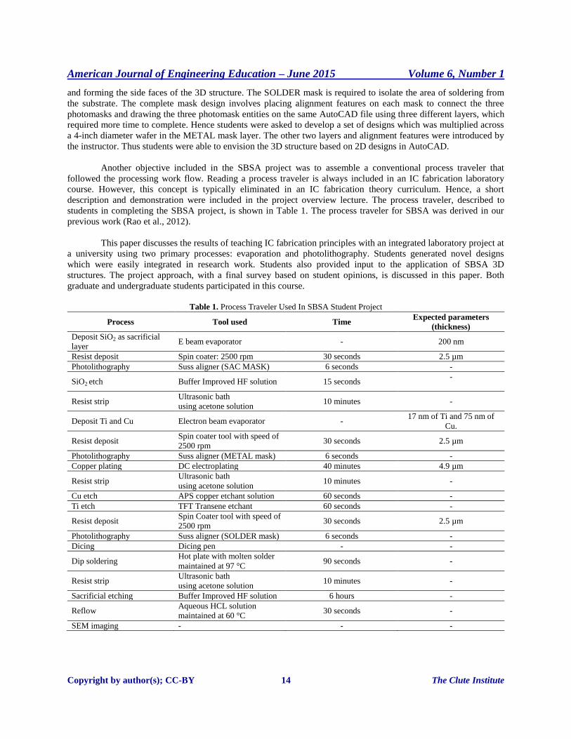
students in completing the SBSA project, is shown in Table 1. The process traveler for SBSA was derived in our
previous work (Rao et al., 2012).
This paper discusses the results of teaching IC fabrication principles with an integrated laboratory project at
a university using two primary processes: evaporation and photolithography. Students generated novel designs
which were easily integrated in research work. Students also provided input to the application of SBSA 3D
structures. The project approach, with a final survey based on student opinions, is discussed in this paper. Both
graduate and undergraduate students participated in this course.
Table 1. Process Traveler Used In SBSA Student Project
Process Tool used Time Expected parameters
(thickness)
Deposit SiO2 as sacrificial
layer E beam evaporator - 200 nm
Resist deposit Spin coater: 2500 rpm 30 seconds 2.5 µm
Photolithography Suss aligner (SAC MASK) 6 seconds -
SiO2 etch Buffer Improved HF solution 15 seconds -
Resist strip Ultrasonic bath
using acetone solution 10 minutes -
Deposit Ti and Cu Electron beam evaporator - 17 nm of Ti and 75 nm of
Cu.
Resist deposit Spin coater tool with speed of
2500 rpm 30 seconds 2.5 µm
Photolithography Suss aligner (METAL mask) 6 seconds -
Copper plating DC electroplating 40 minutes 4.9 µm
Resist strip Ultrasonic bath
using acetone solution 10 minutes -
Cu etch APS copper etchant solution 60 seconds -
Ti etch TFT Transene etchant 60 seconds -
Resist deposit Spin Coater tool with speed of
2500 rpm 30 seconds 2.5 µm
Photolithography Suss aligner (SOLDER mask) 6 seconds -
Dicing Dicing pen - -
Dip soldering Hot plate with molten solder
maintained at 97 °C 90 seconds -
Resist strip Ultrasonic bath
using acetone solution 10 minutes -
Sacrificial etching Buffer Improved HF solution 6 hours -
Reflow Aqueous HCL solution
maintained at 60 °C 30 seconds -
SEM imaging - - -
Page 5
American Journal of Engineering Education – June 2015 Volume 6, Number 1
Copyright by author(s); CC-BY 15 The Clute Institute
EXPERIMENTAL PROCEDURES
The laboratory experiments were initiated by forming four groups of students. The students in a group had
equal numbers of undergraduate and graduate students. The group members were selected in a sense that graduate
students took the leadership roles and undergraduate students obtained the necessary research experience. The
groups were given the tasks as shown in Table 2. Table 2 shows that four tasks: mask design, dip soldering, reflow,
and SEM imaging were allotted to all groups. Patterning, deposition, and SEM imaging required pre-requisite
training and certification to use the tool. Hence, the groups were formed to have at least one student with prior
experience and certification in deposition or patterning and SEM usage. Generally, graduate students working in the
area of materials possesses required expertise and certification in the mentioned tools. The processing details, shown
in Table 3, indicate that the individual groups were given tasks to move the project forward. The approach ensured
that individual group's task was bound by time. Each of the processing steps were given a maximum of seven days
to complete.
The SBSA project consists of 14 processes to build 3D structures on a silicon wafer. SBSA includes a few
wet processes including wet etching of SiO2, titanium (Ti), and copper (Cu), resist stripping, and Cu direct current
(DC) electroplating. The wet etching and electroplating processes were handled by the instructor, to avoid
unintentional chemical hazards. The dip soldering and reflow processes were completed by students and monitored
by the instructor.
Table 2. Tasks Allotted To Student Groups
Groups Tasks
1 Mask design, photolithography, dip solder, reflow, and SEM image
2 Mask design, evaporation, dip solder, reflow, and SEM image
3 Mask design, photolithography, dip solder, reflow, and SEM image
4 Mask design, evaporation, dip solder, reflow, and SEM image
Table 3. Processing Steps Followed By Different Groups
Process Operator
Oxide deposition Group1
Photolithography Group2
Wet etching Instructor
Ti and Cu evaporation Group3
Photolithography Group4
Copper plating Instructor
Resist stripping Instructor
Metal etching Instructor
Photolithography Instructor
Dip soldering All groups separately supervised by Instructor
Dicing Instructor
Sacrificial etching Instructor
Reflow All groups separately supervised by Instructor
SEM imaging All groups
Brainstorming Session To Produce Mask Design
A brainstorming session on the SBSA project was included as a part of the laboratory project. A 30 minute
lecture was given on the overview of the SBSA project and followed by a brainstorming session for 20 minutes.
Students were shown the process traveler, mentioned in Table 1, and a few research results were provided to initiate
the brainstorming between students within their group. Brainstorming was included to find innovative 2D pattern
designs developed by students. The 3D folding success of regular square faces and truncated square faces were
shown to students and are depicted in Figure 1 (Rao et al., 2012). The student groups were evaluated based on at
least five innovative face designs for a fixed nominal (linear) length of 300 μm and a fixed base length of 300 μm.
The nominal length and base length are best described in Figure 2. The six best face designs were chosen by the
instructor and were shared with students. Students were asked to design the six selected face designs on four
different variants (three sided base to six sided base). The final design was completed in AutoCAD software.
Page 6
American Journal of Engineering Education – June 2015 Volume 6, Number 1
Copyright by author(s); CC-BY 16 The Clute Institute
Additional out-of-class help was provided to answer any student questions. The final student designs were verified
and assembled in a single layer and labeled as the METAL mask by the instructor. Two additional mask designs:
SAC mask to perform sacrificial etching and SOLDER mask to do selective soldering on the metal patterns, were
designed by the instructor and were sent for mask production.
Figure 1. Folding Yields For Face-Soldered Polyhedra At Two Different Gap Spacings. The Face Thickness Is Fixed At 4.9 m.
Figure 2. Picture Used To Demonstrate The Difference Between Nominal, Actual And Base Length.
Page 7
American Journal of Engineering Education – June 2015 Volume 6, Number 1
Copyright by author(s); CC-BY 17 The Clute Institute
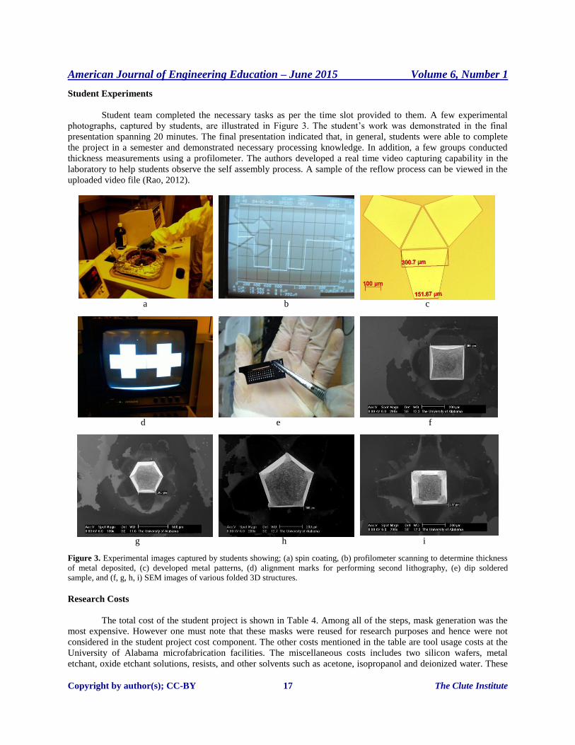
Student Experiments
Student team completed the necessary tasks as per the time slot provided to them. A few experimental
photographs, captured by students, are illustrated in Figure 3. The student’s work was demonstrated in the final
presentation spanning 20 minutes. The final presentation indicated that, in general, students were able to complete
the project in a semester and demonstrated necessary processing knowledge. In addition, a few groups conducted
thickness measurements using a profilometer. The authors developed a real time video capturing capability in the
laboratory to help students observe the self assembly process. A sample of the reflow process can be viewed in the
uploaded video file (Rao, 2012).
Figure 3. Experimental images captured by students showing; (a) spin coating, (b) profilometer scanning to determine thickness
of metal deposited, (c) developed metal patterns, (d) alignment marks for performing second lithography, (e) dip soldered
sample, and (f, g, h, i) SEM images of various folded 3D structures.
Research Costs
The total cost of the student project is shown in Table 4. Among all of the steps, mask generation was the
most expensive. However one must note that these masks were reused for research purposes and hence were not
considered in the student project cost component. The other costs mentioned in the table are tool usage costs at the
University of Alabama microfabrication facilities. The miscellaneous costs includes two silicon wafers, metal
etchant, oxide etchant solutions, resists, and other solvents such as acetone, isopropanol and deionized water. These
a b c
d
g h i
e f
Page 8
American Journal of Engineering Education – June 2015 Volume 6, Number 1
Copyright by author(s); CC-BY 18 The Clute Institute
solutions and wafers were a part of the materials purchased for research and thus the cost was not factored into the
student laboratory project. Overall the student project cost was $640 USD which includes evaporation, patterning
and SEM usage.
Table 4. Cost Of The Project
Steps Costs (USD)
Masks 1500
Evaporation 120
Patterning 120
SEM imaging 400
Miscellaneous 200
Assessment
A survey containing various questions and suggestions to improve the laboratory component in the course
was given to students in the class. Student feedback is considered the best and time effective assessment tool in
undergraduate and graduate teaching (Lazic et al., 2010). Students answered the feedback questions in the form of
ratings ranging from 1 to 5, where 1 and 2 indicated negative responses and 4 and 5 indicated positive responses.
The option of 3, indicating a neutral response, was also provided in the survey. Ratings of 4 and 5 were grouped
together and 1 and 2 ratings were grouped together for positive and negative response markers, respectively. The
survey results were analyzed to improve the laboratory part for future semesters.
EXPERIMENTAL RESULTS
Brainstorming Session To Produce Mask Design
The brainstorming session led to different student designs drawn on paper as shown in Figure 4. This
shows that a lecture of 30 minutes prompted groups of students to develop at least six designs. A few designs were
common between the groups. Six popular designs were selected by the instructor and students provided the primitive
designs in AutoCAD software. The six common designs were labeled: rounded-corner, hour-glass, trumpet, trash
can, semi circle, and funnel. The final mask design provided by students is shown in Figure 5. The figure shows that
the selected designs were repeated for four variants. The student’s mask designs were later arranged in a new CAD
file. Two other layer designs: SAC and SOLDER were wrapped along the students mask design and sent for mask
generation. Three glass masks with six novel designs were produced from the student brainstorming session.
Page 9
American Journal of Engineering Education – June 2015 Volume 6, Number 1
Copyright by author(s); CC-BY 19 The Clute Institute
Figure 4. Picture showing design by group of students during brainstorming session in class. Note that the diagrams are not to
scale. Six designs: (a) rounded-corner, (b) hour-glass, (c) trumpet, (d) trash-can, (e) semi-circle, and (f) funnel are shown.
a b
c d
e f
Page 10
American Journal of Engineering Education – June 2015 Volume 6, Number 1
Copyright by author(s); CC-BY 20 The Clute Institute
Figure 5. Picture showing (a) mask design developed by the instructor and (b) mask design developed by student groups. Six
designs starting from left to right: rounded-corner, hour-glass, trumpet, trash-can, semi-circle, and funnel are shown.
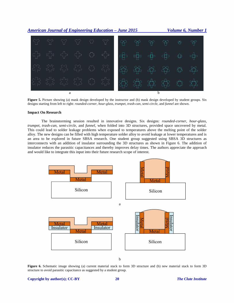
Impact On Research
The brainstorming session resulted in innovative designs. Six designs: rounded-corner, hour-glass,
trumpet, trash-can, semi-circle, and funnel, when folded into 3D structures, provided space uncovered by metal.
This could lead to solder leakage problems when exposed to temperatures above the melting point of the solder
alloy. The new designs can be filled with high temperature solder alloy to avoid leakage at lower temperatures and is
an area to be explored in future SBSA research. One student group suggested using SBSA 3D structures as
interconnects with an addition of insulator surrounding the 3D structures as shown in Figure 6. The addition of
insulator reduces the parasitic capacitances and thereby improves delay times. The authors appreciate the approach
and would like to integrate this input into their future research scope of interest.
Figure 6. Schematic image showing (a) current material stack to form 3D structure and (b) new material stack to form 3D
structure to avoid parasitic capacitance as suggested by a student group.
a
b
a b
Page 11
American Journal of Engineering Education – June 2015 Volume 6, Number 1
Copyright by author(s); CC-BY 21 The Clute Institute
Finally, folding and bridging yields of the student’s designs were determined. Bridging refers to hinging of
all metal faces with the central metal face. Bridging yield was evaluated by visual inspection in a SEM for the
number of entities which showed complete hinging. Folding yield was evaluated for only successfully bridged
patterns. The unbridged patterns were ignored for folding evaluation. Folding yield was estimated by visual
inspection in a SEM for the number of successfully folded 3D structures. Figure 7 shows bridging and folding yields
of the student designs. The rounded-corner design showed higher bridging yield than the rest and the funnel design
showed lower bridging results. In the folding results, the trumpet design showed consistent results compared to the
rest. Further research on the geometry of the funnel design and trumpet design will be conducted in the future.
Figure 7. (a) Bridging and (b) folding yields of patterns designed by students in the course.
Assessment Results
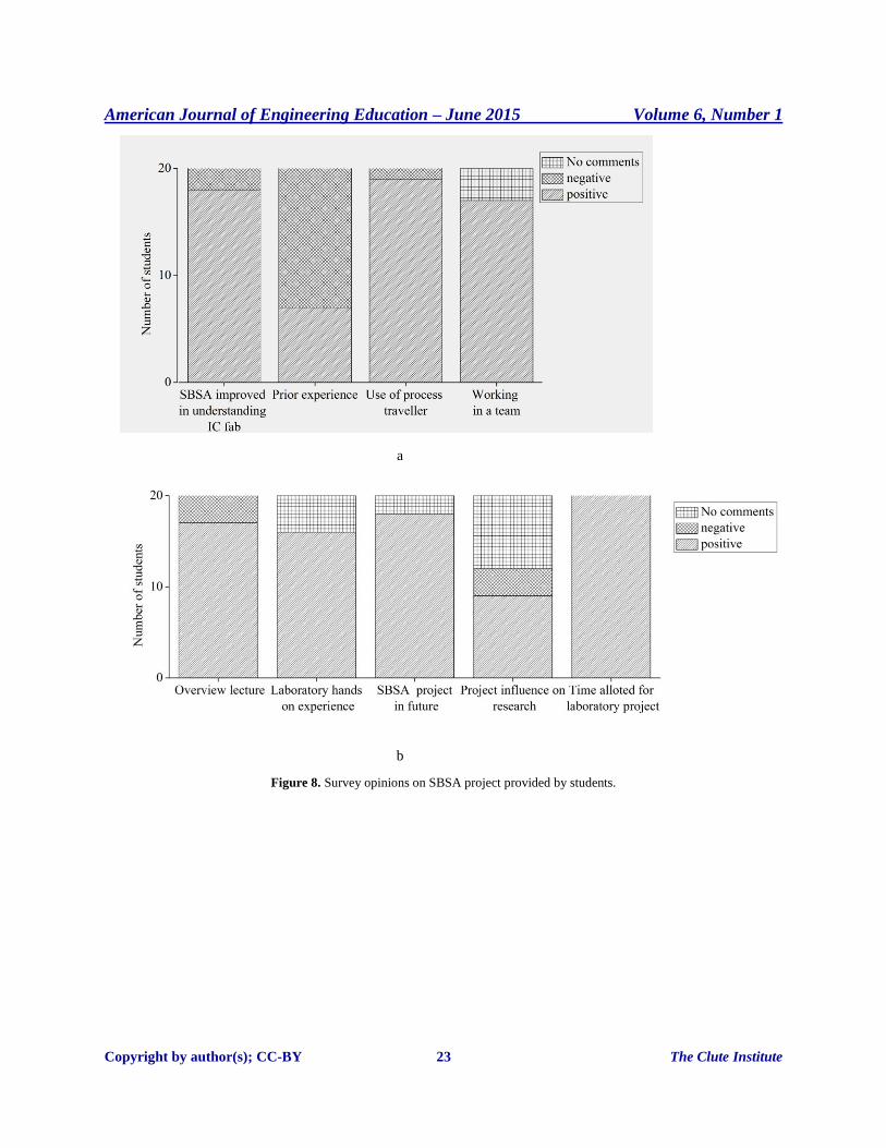
The survey results shown in Figure 8 (a) suggests that although prior experience of silicon processing
among students were low, the SBSA project in the laboratory helped students understand IC fabrication principles
well. The majority of students enjoyed working in a team, which is crucial for their professional development in the
future. The students followed the process traveler and demonstrated an understanding of the traveler. Most engineers
in the semiconductor industries are required to follow an established traveler. Figure 8 (b) suggests that a majority of
students were positive about the overview lecture provided describing the project. A majority of students were
satisfied with the laboratory hands-on experience in regards to completing this project. Students recommended a
similar project for future IC fabrication courses. Students were pleased with the time dedicated for the project.
a
b
Page 12
American Journal of Engineering Education – June 2015 Volume 6, Number 1
Copyright by author(s); CC-BY 22 The Clute Institute
However, student opinions on research related to self assembly were not completely positive. Hence the integration
of SBSA project in a IC fabrication course failed to influence students, to pursue more self assembly research. The
authors believe that students do not appreciate the natural self assembly process as a technological innovation and
hence student interest in the area of self assembly research was low. Due to time limitations, the instructor was
unable to discuss the applications of self-assembled 3D structures in the microelectronics field and may have added
to the low interest rating for students.
Figure 9 shows that students enjoyed SEM imaging and reflow processing steps compared to other
processing steps in the SBSA project. The reflow process included a video recording of the folding process for
micro-scale 3D structures. The video capturing facility was set up by the instructor using a super-macro lens and an
optical camera. The real-time folding of micro-scale 2D metal faces was viewed clearly via the video setup and
hence student’s positive rating was justified. SEM imaging was the final step in the project, where students observed
successfully folded or failed 3D structures, hence a positive rating for the SEM imaging step was expected. Students
gave a low rating to mask design. The mask design using AutoCAD software has a high learning curve. An expert
mask designer normally uses an available template and modifies the existing template to develop new designs. Most
of the students were novice users of AutoCAD software and this may have possibly led to low ratings. Evaporation,
due to the time intensive nature, was rated low compared to other steps involved in the laboratory project. This was
especially true for students performing Ti and Cu evaporation spending 4 hours on a single step compared to the
reflow step of 30 minutes, SEM imaging of 30 minutes, and lithography of around 1 hour. Hence, the low interest in
evaporation was understood. The low interest in dip soldering process was unexpected since the time taken to
complete the dip soldering process was less than 10 minutes. The authors believe that students found the process to
be trivial and that it did not offer any new learning component. The dip soldering process involved cleaning samples
in acidic flux which needed certain safety precautions to be undertaken by the student to perform this step. The
authors believed that these precautions acted as overhead for a trivial process and reduced the student ratings.
Time Spent By Instructor
The time spent on the overall processing steps starting with formation of student groups to the student
presentation is shown in Table 5. A total of 20.25 hours was devoted by the instructor in supervising and providing
patterns to complete the laboratory project besides teaching the IC fabrication theory course. However with close to
20 hours of supervision and an average time of less than 5 hours spent by individual students, the laboratory project
was seen as a time appropriate process to be included in any future IC fabrication curriculum.
CONCLUSIONS
The brainstorming session demonstrated six novel designs produced by students. Students, in groups,
demonstrated required CAD skills to design the photomask. Given more time, students could have designed a
complete set of photomasks. Students showed interest by providing a few improved design suggestions to avoid
fringing capacitance for 3D structures to be used as 3D interconnects. This demonstrated that students showed
interest and provided valuable feedback to the self-assembly research topic. Student assessment results indicated that
the SBSA project was an interesting topic to be included in a IC fabrication theory curriculum. Various aspects of
student learning outcomes, in the form of ABET's (a-k), were successfully achieved. The SBSA project was found to
be time appropriate and cost effective to be included in a future IC fabrication theory course. The authors realized
that a few tasks, such as evaporation of Ti and Cu, will be included as an instructor activity since evaporation is the
most time consuming step in this project and students tend to lose interest in this step. Overall, the SBSA project
was a perfect fit to include laboratory hands-on experience with the IC fabrication theory class in a semester.
Page 13
American Journal of Engineering Education – June 2015 Volume 6, Number 1
Copyright by author(s); CC-BY 23 The Clute Institute
Figure 8. Survey opinions on SBSA project provided by students.
b
a
Page 14
American Journal of Engineering Education – June 2015 Volume 6, Number 1
Copyright by author(s); CC-BY 24 The Clute Institute
Figure 9. Survey opinions showing the number of students liked each individual processing steps in SBSA project.
Table 5. Time Spent By Instructor On The Laboratory Project.
Steps Time (hours)
Formation of student groups 1
Brainstorming session 2
Designing masks 3
Wet etching 0.25
Copper plating 2
Resist stripping 0.25
Metal etching 0.25
Photolithography 1
Dip soldering 2
Dicing 0.25
Sacrificial etching 0.25
Reflow 2
Evaluation of presentation and work 4
ACKNOWLEDGEMENTS
The authors would like to acknowledge the support of The University of Alabama Central Analytical and the
Microfabrication Facilities.
AUTHOR INFORMATION
Madhav Rao completed his Masters in Microelectronics and Photonics from University of Arkansas in 2007 and
Ph.D in Electrical and Computer Engineering department from the University of Alabama in 2012. He joined IIIT-
Bangalore as faculty after graduation. His major research contributions are in the area of solder based self assembly
technology, 3D antennas, magnetic logic devices and Carbon nanotubes filled silicon vias. He has interest in taking
emerging technologies to the classrooms to keep the curriculum updated and interesting to students.
Page 15
American Journal of Engineering Education – June 2015 Volume 6, Number 1
Copyright by author(s); CC-BY 25 The Clute Institute
Susan Burkett is the Alabama Power Foundation Endowed Professor in Electrical and Computer Engineering at
The University of Alabama. She received her B.S., M.S., and Ph.D. degrees in Electrical Engineering from the
University of Missouri in Columbia, Missouri. She teaches courses in circuit analysis, integrated circuit fabrication,
and senior design. She served as Program Director at the National Science Foundation (NSF) in the Division of
Undergraduate (DUE) Education from 2005-2007. Professor Burkett is a member of ASEE, AVS: Science and
Technology Society, and a senior member of IEEE.
John Lusth is an Associate Professor of Computer Science and the Director of the First Year in Computing at The
University of Alabama. He received his B.S. in Chemistry at Michigan Technological University, a M.S. in
Computer Science at Duke University, and a Ph.D. in Computer Science at The University of Alabama. He teaches
the introductory Computer Science course as well as Programming Languages and Computer-assisted Music
Composition and Generation.
REFERENCES
Hong, S. J., & Ha, T. M. (2013). Hands-on experience-based microelectronics manufacturing engineering education.
2013 IEEE International Conference on Teaching, Assessment and Learning for Engineering (TALE) (p.
277-282).
Voros, K. (2014). The UC Berkeley IC Lab. IEEE Solid-State Circuits Magazine, 6(2), 25-34.
Hunt, D. J. (2006, june). Low Budget Undergraduate Microelectronics Laboratory. 2006 16th Biennial
University/Government/Industry Microelectronics Symposium (p. 81-87).
Naseem, H., A., & Brown, W., D. (1999). Integrated Circuit fabrication technology and laboratory courses at the
University of Arkansas. Proceedings of the Thirteenth Biennial University/Government/Industry
Microelectronics Symposium (p. 6-9).
Parke, S., Burkett, S., Duttagupta, S., Honfhine, M., Erickson, G., Holscher, R., Boorom, K., Rosato, J., & Clifford,
R. (1999). Microelectronics education and research in the Idaho Microfabrication Laboratory at Boise State
University. Proceedings of the Thirteenth Biennial University/Government/IndustryMicroelectronics
Symposium (p. 17-21).
Pan, K., Yang, D., Kai, Q., Zhang, K., & Yang, L. (2008, july). Introduction of Microelectronics Manufacturing
Engineering into professional education: a joint effort among industry, government and universities. 2008
ICEPT-HDP International Conference on Electronic Packaging Technology & High Density Packaging (p.
1-5).
Allen, P., Strader, N. I., & Geiger, R. (1982, mar). Graduate and undergraduate educational methods for
microelectronics. IEEE transactions on components, hybrids, and manufacturing technology, 5 (1), 105 -
111.
Fuller, L., & Hirschman, K. (1997). Teaching cmos integrated circuit manufacturing laboratory using a student
operated factory. In Proceedings of the twelfth biennial university/government/industry microelectronics
symposium (p. 36-39).
Gracias, D. H., Kavthekar, V., Love, J. C., Paul, K. E., & Whitesides, G. M. (2002). Fabrication of micrometer-
scale, patterned polyhedra by self-assembly. Advanced Materials, 14 (3), 235–238.
Gracias, D. H., Tien, J., Breen, T. L., Hsu, C., & Whitesides, G. M. (2000, 08/18). Forming electrical networks in
three dimensions by self-assembly. Science, 289 (5482), 1170–1172.
Yang, L., Liu, W., Wang, C., & Tian, Y. (2011, aug). Self-assembly of three-dimensional microstructures in MEMS
via fluxless laser reflow soldering. 2011 12th International Conference on Electronic Packaging
Technology and High Density Packaging (ICEPT-HDP), (p 1-4).
Kong, M., Jeon, S., Au, H., Hwang, C., & Lee, Y-C. (2011, october). Development and Experimental Validation of
a 3-D Solder Self-Alignment Model for Alignment Accuracy Prediction of Flip-Chip Assembly. IEEE
transactions on Components, Packaging and Manufacturing Technology, 1(10) 1523.
Yang, L., Wang, C., Liu, W., & Tian, Y. (2012, aug). Dynamic model for analyzing the motion of molten solder
during self-assembly. 2012 13th International conference of Electronic Packaging Technology and High
Density Packaging (ICEPT-HDP), ( p 649-652).
Harsh, K., & Lee, Y. C. (1998). Modeling for solder self-assembled mems. In Proceedings of the spie conference,
(p. 177).
Page 16
American Journal of Engineering Education – June 2015 Volume 6, Number 1
Copyright by author(s); CC-BY 26 The Clute Institute
He, H., Guan, J., & Lee, J. L. (2006, 1/10). An oral delivery device based on self-folding hydrogels. J. Controlled
Release, 110 (2), 339.
Howe, R. T. (1988, 11). Surface micromachining for microsensors and microactuators. In 32nd international
symposium on electron, ion and photon beams (p. 1809).
Khaliq, M. A. (2001). Undergraduate microelectronics education in engineering and technology programs at
minnesota state university, mankato. In Proceedings of the fourteenth biennial
university/government/industry microelectronics symposium (p. 28-32).
Lazic, J. L., Pavlina, K., & Pongrac, A. (2010). Teaching quality - student perspective. In Proceedings of the 33rd
international convention (p. 812-814).
Mirkin, C. A., Letsinger, R. L., Mucic, R. C., & Storhoff, J. J. (1996, 08/15). A dna-based
method for rationally assembling nanoparticles into macroscopic materials. Nature 382 (6592), 607–9.
Neudeck, G., Anderson, R. M., & Silva, L. F. (1971, june). The teaching of integrated circuits: Analysis, design, and
fabrication. Proceedings of the IEEE, 59 (6), 990- 992.
Oraon, N., Kumar, P., Srivastava, C., & Rao, M. (2013). Self assembly based 3d heatsink antenna for high density
3d integration. In International ieee conference of circuits, controls, and communication (p. 1-5).
Oslapas, A. (1993, nov). Beyond brainstorming: Creative problem-solving techniques. In Proceedings of twenty-
third annual conference frontiers in education conference’engineering education: Renewing america’s
technology’ (p. 837).
Parent, D., Basham, E., Dessouky, Y., Gleixner, S., Young, G., & Allen, E. (2005, aug.). Improvements to a
microelectronic design and fabrication course. IEEE Transactions on Education, 48 (3), 497-502.
Park, J. Y., Kim, K. T., Sung, M. S., & Pak, J. J. (2003). 3d mems antenna for ir sensor using novel uv-lithography,
plastic micromachining and mesh structure bonding technique. In Proc. int. conf. on optical mems. (p. 79).
Randall, C. L., Leong, T. G., Bassik, N., & Gracias, D. H. (2007). 3d lithographically fabricated nanoliter containers
for drug delivery. Adv. Drug Deliv. Rev., 59 (15), 1547–61.
Rao, M. (2012). Available: http://unix.eng.ua.edu/~mrrao/trsqpyHiDef.wmv. ([Online])
Rao, M., Lusth, J. C., & Burkett, S. L. (2009). Self-assembly solder process to form three-dimensional structures. J.
Vac. Sci. Technol. B, 27 (1), 76-81.
Rao, M., Lusth, J. C., & Burkett, S. L. (2011). Analysis of a dip-solder process for self-assembly. J. Vac. Sci.
Technol. B, 29 (4), 042003-042011.
Rao, M., Lusth, J. C., & Burkett, S. L. (2012). A study of solder bridging for the purpose of assembling three
dimensional structures. J. Vac. Sci. Technol. B, 30 (3), 032001-032012.
Rao, M., Lusth, J. C., & Burkett, S. L. (2013). Demonstration of electrical connectivity between self assembled
structures. J. Vac. Sci. Technol. B, 31 (3), 032002-032012.
Shanableh, A., Omar, M., Younes, B., & Barakat, S. (2003). Perceptions on effective engineering education. In 33rd
annual frontiers in education (p. S4B-1-6).
Yan-Ming, W. (2010). Group learning for different major undergraduate students in public selective course. In
International conference on educational and information technology (iceit) (Vol. 3, p. V3-407 -V3-410).