52
I PC1512 PERSONAL COMPUTER PC-MM MONOCHROME MONITOR PC-CM COLOUR MONITOR SERVICE MANUAL

IPC1512
PERSONAL COMPUTERPC-MM
MONOCHROME MONITORPC-CM
COLOUR MONITOR
SERVICE MANUAL
CONTENTSSafety NoteTechnical Specification
Servicing NoteFD-3 Flow ChartFD-3 Flow ChartFD-3 Servicing Information
FD-3 Exploded ViewCabinet Diagram Exploded View & Parts List
Electrical Parts List
Cabinet Diagram Exploded ViewCPU P.C.B. Assembly Component SideExploded View CPU Unit
Hard Disc Installation Instructions
Alignment Instructions PC-CMAlignment Instructions PC-MM/PC1512Cabinet Diagram & Parts List PC-CMCabinet Diagram & Parts List PC-MMChassis Schematic DiagramKeyboard Schematic Diagram & P.C.B. LayoutKeyboard Exploded ViewChassis Schematic Diagram PC-MMChassis Schematic DiagramChassis Schematic DiagramChassis Schematic Diagram PC-MM MonitorChassis Schematic DiagramPC-CM Power SupplyPC-CM Main PCB Component LayoutPC-CM Main PCB Component LayoutCRT PC Board, Colour MonitorSchematic Diagram FD-3 CPU
Page
2
2
33
4-67- 14
1516& 1718-20
21
22 &23242526272829
30-3334&35
363738394041
42434344
TECHNICAL SPECIFICATION
51 2K system unit with all circuitry on a single motherboard.8MHz 8086 processor.
Memory expandable on motherboard to 640K.Integral colour graphics adaptor with special 16 colour hi-res
mode.Three full-size compatible expansion slots with power available
in the standard unit to supply a hard disc and controller.
Choice of one or two 360K 5 1A" floppy discs or one floppy with a
1 or 20 megabyte hard disc drive.
HARD DISC VERSIONS ARE SUPPLIED WITH AN EXTRAFLOPPY DISC AND MANUAL WITH BACKUP, RESTORE ANDFORMAT UTILITIES.Motherboard includes an RS232c serial and parallel interface
with standard connectors.Loudspeaker with volume control.
Battery-backed real time clock and configuratioon RAM.Socket for 8087 maths co-processor.
Connector for light pen.
Complete with Colour Monitor or Monochrome (Grey Level)
Monitor.
The standard built-in colour adaptor provides all the following
modes.Medium resolution Alpha; 16 colours, 40x45 characters.
High resolution Alpha; 16 colours, 80x25 characters. .^Medium resolution Graphics; 2 colour, Three 4-colour pallettes,
320x200 pixels.
High resolution Graphics; 2 colour, 640x200 pixels.
-FSpecial high-res Graphics; 16 colours, 640x200 pixels.
Full size QWERTY keyboard.
Illuminated Numlock and Capslock.Keyboard joystock port.
Extra DEL-» and ENTER keys.
Two button Mouse with
Dedicated port on system unit.
Microsoft compatible MOUSE.COM plus special text operation.
DIMENSIONS (all in mm)PC1 51 2SD System unit 372(w) x 384(d) x 1 35(h) 6.05KgPC1512DD System unit 372(w) x 384(d) x 135(h) 7.75KgKeyboard Unit inc feet 465(w) x 1 60(d) x 58(h) 1 .1 75KgPC-MM Monochrome Monitor 350(w) x 300(d) x 31 5(h) 7.43KgPC-CM Colour Monitor 372(w) x 365(d) x 330(h) 1 1.6Kg
SAFETY TEST
All monitors are safety tested to the following specifications.
1). Flash TestTest at 3kV between the live and neutral of the mains lead joined together andand ALL accessible metal points on the exterior of the set.
2). Insulation Resistance TestTest between the live and neutral of the mains lead joined together and ALLaccessible metal points on the exterior of the set to show a resistance of at
least 4Mohm.
If after servicing there is any doubt about continued electrical safety the abovetests should be carried out.
AMSTRAD pic
BRENTWOOD HOUSE, 169 KINGS ROAD, BRENTWOOD, ESSEX CM14 4EF.
TELEPHONE; 0277 230222. TELEX: 995417 AMSELE G.

NOTE
THE FLOWCHARTS ARE FOR INFORMATION ONLY AND FOR WARRANTY PURPOSES ANY FAULTYDRIVE MECHANISM MUST BE RETURNED TO AMSTRAD FOR REPLACEMENT. SERVICE AGENTSSHOULD NOT ATTEMPT TO REPAIR THE MECHANISM.SERVICE AGENTS SHOULD NOTE THAT THE HARD DISC UNITS ARE THE MOST SOPHISTICATEDMECHANISMS AND SHOULD NEVER BE OPENED IN A NORMAL ENVIRONMENT. IF ANY ATTEMPTSARE MADE TO OPEN THE HARD DISC UNITTHE GUARANTEE IS THEN INVALIDATED AND AMSTRADTAKES NO RESPONSIBILITY TO EXCHANGE THE DRIVE.
YOU SHOULD NOTE FURTHER THAT THERE ARE TWO TYPES OF HARD DISC UNITS IN USEi.e. XEBEC AND TANDON. WHEN ORDERING THE REPLACEMENT UNITS MAKE SURE THAT THEPART NO. IS EITHER 171663/X FOR XEBEC DRIVE OR 171663/T FOR TANDON DRIVE. THISINFORMATION APPLIES ONLY TO THE 20MB DRIVES.
AMSTRAD RESERVES THE RIGHT TO AMMEND THE CIRCUIT OR CHANGE THE COMPONENTSWITHOUT PRIOR WARNING.USE RP4 DIAGNOSTICS EXPANSION CARD OR DIAGNOSTIC DISC FOR FAULT FINDINGS.
FD-3 SERVICE INFORMATION
1. Introduction
This section is for the maintenance of DFC222A.
1-1 General
The floppy disk drive is a high precision equipment and requires the following jigs, tools, measuringinstruments, and adjustments when repairing or changing parts.
2. Special Jigs, Tools and Measuring Instruments
2-1 List of Special Jigs and Tools
CE diskette
Blank diskette
Test pin connectorAlignment adjusting jig
O track adjusting jig
2-2 List of Measuring Instruments
OscilloscopeBrikonFrequency counter
2-3 CE Diskette (Alignment Diskette)
This diskette is used for the following adjustments and inspection.
(1) R/W head radial position
(2) R/W head azimuth
(3) Index position
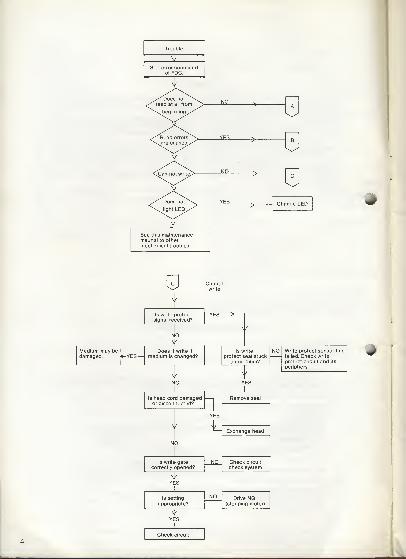
Trouble
3£See error command
of FDC.
See this maintenancemaunal to othermechanical troubles.
NO
YES ->-
Nn
YES->- Change LED
V
Is write protect
signal received?
Medium may bedamaged. •-YES—
NO
Does it write if
medium is changed?
YNO
Cannotwrite
YES-
\/
Is write
protect seal stuck
on medium?
NO
YYES
Write protect sensor hasfailed. Check write
protect circuit and its
periphery.
J
Is head cord damagedor disconnected?
V
NO
Remove seal
YES
Exchange head
Is write gatecorrectly opened?
YES
_L_Is setting
appropriate?
YES
NO
NO
Check circuit
check system
Drive NG(stepping motor)
Check circuit

±Is termination
resistor correctly
attached?
NO Mountcorrectly
YES
1_Is environment
condition appropriate?NO Set up environmental
condition appropriately
YES
Are errors
caused after changingto another medium?
NO Medium maybe faulty
YES
Is a verylarge noise source
present?
YES Remove noisesource
NOIs tlkere
&Is there
sufficient headhead pressure
NO
NO Change head
YES
Are errors
caused on inner
circumference of
tracks?
NO
YES
Is spindle
speed OK?NO
YES
Is indexsignal correctly sent?
NO Adjustment
YES
\l/
Is azimuthazimuth
NO Tilting of guide shafts
due to shock, or headsare defective
YES
Is seekoperationnormal?
NO > Check step motor anddriving mechanism
YES
Is time marginof inner circumference
tracks sufficient?
YES
ANO
YES
^_
^LChange the printed
circuit board. Changethe head if problem
is not solved.
Is power NO Check powerripple noisecorrectly fed?
Check data separatoron system side
YES
vCheck circuit
(Read errors are caused)

FD-3 FLOWCHART
Are connectorscorrectly plugged?
NO .. Plug correctly
r>Medium maybe faulty
YES
NO ^Is short bar
setting correctly?
Set normally>
YES
YES
YES
sk_
Does it readif changed to
another medium?
NO
Is alignmentOK?
YES
Is spindle
speed OK?
YES
1_Is index signal
sent correctly?
YES
XL.
Is TRKOO OK?
YES
Is motor start
time appropriate?
YES
Is mediumrotating?
NO-
J1L.
Does cariage
operate properly?
NO. Check step motorand circuit head
driving mechanismoperating step
motor.
YES
Does readwaveform show
after adjustment?
YES Adjustment,
NO
NOi
V
NO
V
NO
Read circuit mayhave problems.
Change MC3470AP.Change printed
circuit board.
V
NO
V
Over-speeding?
YES
Check motorcontrol printed
circuit board. Is
servo corddisconnectedfrom motor?
V
Is index sent?
YES
Index sensoris faulty
Adjust
NO
V
-NO
Change motor
alignment
3lRead circuit has
a problem.
ExchangeMC3470AP.
Change printer
circuit board.
XL.
Operatingnormally?
Possibility of
or head cord
trouble.
Adjust
X-
Adjust
V
Can it beadjusted?
V
NO
NO
XLIs power fed? NO Check power
YES
ADoes DC motor
operate?(Apply 12V)
NO^ Change DC motor *YES
J/
NO^Are cords
and wires correctly
connected?
Correct
incorrect wiring.
YES
-YESI OK
Is motor ONsignal sent?
NO. Check signal onsystem side
YES
*_Possibility of circuit
part faults. Adjust
centering motor-control
printed circuit board.
W
-YES- OK
Drive has problem(Medium slip or
other reason).

3. Diagnosis Procedure
3-1 General
Errors caused by an incorrect operating procedure, erroneous programming, damaged diskette,and sott errors caused by dirty air, random electric noise, and other external factors are oftenconsidered to be drive failures or incorrect adjustments. Check that errors are repetitively
produced with the first diskette and that similar errors are also produced with other diskettes,unless obvious assembly trouble and damage are found in visual inspection.
3-2 Soft Error Detection and Correction
Soft errors are generally caused by the following.
(1) Dirty air between the R/W head and disk. Normally, this dirt is cleaned by the liner in the diskette.
(2) Random electrical noise less than several microseconds.
(3) Delicate track misalignment and writing timing misalignment that are not detected duringwriting may cause soft errors during reading.
(4) Improper ground of the drive or host system power supply.
(5) Improper motor speed.
The following actions are required on the control side to recover the foregoing soft errors.
(1) Reread the track ten times or until data recovers.
(2) Access the head to an adjacent track in the same direction as the track if the error is notrecovered by Step 1. Then return the head to the previous track.
(3) Repeat Step 1.
(4) Errors that cannot be recovered after taking these steps cannot be recovered.
3-3 Write Error
Operate READ-AFTER-WRITE if an error occurs during the write operation.If the error cannot be recovered after operating READ-AFTER-WRITE more than four times,operate READ-AFTER-WRITE on another track to determine whether the diskette or drive is
responsible for the error. Change the diskette and repeat these steps if the same error remains. If
the error still remains, the drive has some fault and if the error is erased, the diskette is defectiveand should be discarded.
3-4 Read Error
Most errors are soft errors. Data can be recovered by following the error recovery steps (3-2).
3-5 Seek Error
(1) Trouble with the stepping motor or stepping motor drive circuit.
(2) Carriage trouble.
Seek error is recovered by system soft. There are two recovering ways.
(1) Recalibrate
(2) Detect ID field
3-6 Compatibility Error
In some cases, data written by one drive cannot be read by another drive. This is dur mainly to thefollowing reasons:
The check points are listed below.
(1) Improper head alignment — 5-2
(2) The head output is low — 5-6
(3) Motor speed irregularity — 5-1
(4) Check if the recommended sector format is set up.
3-7 List of Test Points (see figure 3-7)
Test Point Signal Name
TP1 AMP OUT +TP2 AMP OUT-TP3 GNDTP4 STEPTP5 READ DATATP6 INDEXTP7 WRITE PROTECTTP8 TRACKTP9 GND
3Fig. 3-7 Test Point Layout
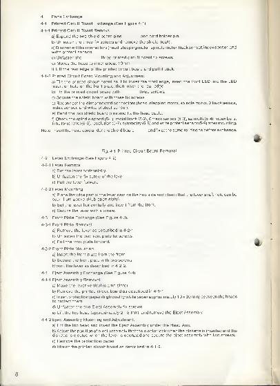
4. Parts Exchange
4-1 Printed Circuit Board Exchange (See Figure 4-1)
4-1-1 Printed Circuit Board Removal
a) Expand the two shield board pins and cord holder pin.
b) Unfasten the three fix screws and remove the shield board.
c) Disconnect the connectors (head, stepping motor, spindle motor, track sensor, index sensor, andwrite protect sensor).
d) Unfasten the three printed circuit board fix screws.
e) Moves '.he head to inner about 10mm.
f) Lift the rear edge of the printed circuit board and pull it back.
4-1-2 Printed Circuit Board Mounting and Adjustment
a) Tilt the printed circuit board as if to lower the front edge, insert the front LED into the LEDinsertion hole on the front plate, then lower the rear edge.
b) Fix the printed circuit board with three screws.
c) Secure the shield board with three fix screws.
d) Reconnect the disconnected connectors (head, stepping motor, spindle motor, track sensor,
index sensor, and write protect sensor).
e) Bend the two shield board pins and fix the head cable.
f) Check the spindle speed (5-1), radial track (5-2), track sensor (5-3), azimuth (5-4), index burst
time (5-5), level (5-6), resolution (5-7), symmetry (5-8) and write protect sensor (5-9) after mounting.
Note: Insert the head cord under the shield board and fix at the same routing as before exchange.
Fig. 4-1 Printed Circuit Board Removal
4-2 Lever Exchange (See Figure 4-2)
4-2-1 Lever Removal
a) Set the lever horizontally.
b) Unfasten the fix screw of the lever.
c) Pull the lever forward.
4-2-2 Lever Mounting
a) Place the wide part of the lever cam on the hub side and check that the lever shaft hole can beseen from above. (Hub open state).
b) Set the lever horizontally and insert from the front.
c) Secure the lever with a screw.
4-3 Front Plate Exchange (See Figure 4-3).
4-3-1 Front Plate Removal
a) Remove the lever as described in 4-2-1.
b) Unfasten the two front plate fix screws.
c) Pull the front plate forward. ^4-3-2 Front Plate Mounting
a) Insert the front plate from the front.
b) Secure the front plate with two screws.
Mount the lever as described in 4-2-2.
4-4 Eject Assembly Exchange (See Figure 4-4)
4-4-1 Eject Assembly Removal.
a) Make the lever vertical (clamp state).
b) Remove the printed circuit board as described in 4-1-1.
c) Insert protection paper (high quality white paper approximately 10x30 mm) between the headsto protect them.
d) Unfasten the two Eject Assembly fix screws.
e) Lift the top head (approximately 2 - 3 mm), and remove the Eject Assembly.
4-4-2 Eject Assembly Mounting and Adjustment.
a) Lift the top head and insert the Eject Assembly under the Head Arm.
b) Adjust the position of eject assembly that the ejector lock when the diskette is inserted and the
diskette is ejected when the lever is operated and secure the eject assembly with two screws.
c) Remove the protection paper.
d) Mount the printed circuit board as described in 4-1-2.
8

Ilj^
4-5 Lever Frame Assembly Exchange (See Figure 4-5)
4-5-1 Lever Frame Assembly Removal
a) Remove the printed circuit board as described in 4-1-1.
b) Remove the lever as described in 4-2-1.
c) Remove the front plate as described in 4-3-1
.
d) Remove the eject assembly as described in 4-4-1.
e) Unfasten the four lever frame assembly fix screws.
f) Lift the lever frame assembly slightly making sure that the top head is not raised, and remove the
slidinh to the left.
4-5-2 Lever Frame Assembly Jvlounting and Adjustment.
a) Lift the top head slightly and slide the pad mounting part of the lever frame assembly under the
top head.
b) Secure the lever frame assembly with four screws.
c) Mount the eject assembly as described in 4-4-2.
d) Mount the front plate as described in 4-3-2.
e) Mount the lever as described in 4-2-2.
f) Unfasten the two screws of hub shaft holder and centre by moving the hub up and down several
times and secure the two screws.
g) Mount the printed circuit board ad described in 4-1-2.
h) After mounting, adjust the index burst time. (Refer to 5-5).
4-6 Stepping Motor Assembly Exchange (See Figure 4-6)
4-6-1 Stepping Motor Assembly Removal
a) Remove the printed circuit board as described in 4-1-1.
b) Unfasten the head assembly metal belt fix screw.
c) Unfasten the stepping motor belt fix screw and remove the keep plate.
d) Unfasten the two stepping motor assembly fix screws.
e) Lift the stepping motor assembly upward, then slide it to the left to remove from the metal belt.
f) Disconnect the stepping motor assembly cord from the hook.
4-6-2 Stepping Motor Assembly Mounting Adjustment
a) Keep the metal belt in the loop form, insert the stepping motor assembly, mount the metal belt
and keep plate with screws.
b) Align the oval hole of the stepping motor mounting plate with the guide pin and mount the
stepping motor assembly with two screws.Temporary tightening of screws are required.
c) Pull the tip of the metal belt and mount the metal belt on the tip of the head assembly with a screw.
d) Move the head assembly back and forth and check that the metal belt is not twisted. If twisted,
slightly loosen the metal belt fix screws on the stepping motor assembly and head assembly, andmove the head assembly back and forth several times.
Fasten the screws tightly.
e) Place the stepping motor assembly cord on the hook.
f) Mount the printed circuit board as described in 4-1-2.
g) Adjust the radial track after mounting. (Refer to 5-2).
Caution: Do not reuse the metal belt removed from the head assembly.
4-7 Head Assembly Exchange (See Figure 4-7)
4-7-1 Head Assembly Removal
a) Remove the printed circuit board as described in 4-1-1.
b) Remove the lever as described in 4-2-1
.
c) Remove the front plate as described in 4-3-1.
d) Remove the eject assembly as described in 4-4-1.
e) Remove the lever framne assembly as described in 4-5-1
.
f) Remove the stepping motor assembly as described in 4-6-1.
g) Unfasten the PCB post fix screws and remove the PCB post.
h) Unfasten the two screws fastening the guide shaft keepers A and B and remove keepers A and B.
i) Lift the guide shaft rear edge and remove the guide shafts in a backward direction, individually. Becareful not to damage guide shafts or mix the right and left shafts.
j) Carefully remove the head assembly.
4-7-2 Head Assembly Mounting and Adjustment
a) Fit the two guide shafts in the head assembly without mixing the right and left, and mount in the
housing while holding the guide shaft.
b) Secure guide shaft keepers A and B using four screws.

c) Secure the PCB post using screws.
d) Mount the stepping motor assembly as described in 4-6-2.
e) Mount the lever frame assembly as described in 4-5-2.
f) Mount the eject assembly as described in 4-4-2.
g) Mount the front plate as described in 4-3-2.
h) Mount the lever as described in 4-2-2.
i) Place the printed circuit board as described in 4-1-2.
j)Adjustthe radial track(5-2) and index burst time (5-5), and checktheO track sensor(5-3),
azimuth (5-4), level (5-6), resolution (5-7) and symmetry (5-8) after mounting.
4-8 Spindle Motor Assembly Exchange (See Figure 4-8)
4-8-1 Spindle Motor Assembly Removal
a) Remove the printed circuit board as described in 4-1-1.
b) Remove the lever as described in 4-2-1.
c) Remove the front plate as described in 4-3-1.
d) Remove the eject assembly as described in 4-4-1.
e) Remove the lever frame assembly as described in 4-5-1
.
f) Unfasten the four spindle motor fixing screws (three screws on top and one screw onthe bottom).
g) Remove the spindle motor in a downward direction. Be careful not to damage the top surfaces of
the spindle.
4-8-2 Spindle Motor Assembly Mounting Adjustment
a) Secure the spindle motor with four screws. Align the W/P LED approximately the
centre of the housing hole.
b) Mount the lever frame assembly as described in 4-5-2. ^c) Mount the eject assembly as described in 4-4-2.
d) Mount the front plate as described in 4-3-2.
e) Mount the lever as described in 4-2-2.
f) Place the printed circuit board as described in 4-1-2.
g) Adjust the spindle speed (5-1 ), radial track (5-2), track sensor (5-3) and index burst time (5-5)
and check the azimuth (5-4), level (5-6), resolution (5-7), symmetry (5-8) and write protect sensor (5-
9) after mounting.
4-9 Track Sensor Assembly Exchange (See Figure 4-9)
4-9-1 Track Sensor Assembly Removal
a) Remove the printed circuit board as described in 4-1-1.
b) Unfasten the track sensor assembly fix screw.
c) Remove the track sensor assembly.
4-9-2 Track Sensor Assembly Mounting and Adjustment.
a) Mount the track sensor assembly with screws.
Temporary tightening of screws is required.
b) Place the printed circuit board as described in 4-1-2.
c) Adjust the track sensor after mounting. (Refer to 5-3).
4-10 Metal Belt Exchange (See Figure 4-10) ^4101 Metal Removal
a) Remove the printed circuit board as described in 4-1-1.
b) Remove the lever as described in 4-2-1.
c) Remove the front plate as described in 4-3-1.
d) Remove the eject assembly as described in 4-4-1.
e) Remove the lever frame assembly as described in 4-5-1.
f) Remove the stepping motor assembly as described in 4-6-1.
g) Remove the head assembly as described in 4-7-1.
h) Unfasten the metal belt fix screws and remove the metal belt from the head assembly.
4102 Metal Belt Mounting and Adjustment
a) Mount the metal belt on the head assembly using screws. (Be careful of the metal belt direction).
b) Mount the head assembly as described in 4-7-2.
c) Mount the stepping motor assembly as described in 4-6-2.
d) Mount the lever frame assembly as described in 4-5-2
e) Mount the eject assembly as described in 4-4-2.
f) Mount the front plate as described in 4-3-2.
g) Mount the lever as described in 4-2-2.
h) Mount the printed circuit board as described in 4-1-2.
i) Adjust the radial track (refer to 5-2), index burst time (5-5), and track sensor (5-3) after mounting.
10

5. Adjustments and Checks
5-1 Spindle Speed Adjustment
a) Insert and clamp a blank diskette by rotating the motor.
b) Stop on track.
c) Connect the frequency counter to TP6.
d) Rotate the speed adjusting variable resistor on the spindle-motor printed circuit board andadjust so that the counter shows 200 +2 ms.
If the spindle-motor is not an adjusting variable resistor type, check the counter shows200 ±2 ms only and adjusting is unnecessary.
fc^_
5-2 Radial Track Adjustment
a) Insert a CE diskette.
b) Move the head to Track 1 6 and check the cat's-eye waveforms of the top and bottom heads.
c) Adjust as follows if one of the top or bottom heads is not more than 75% in an amplitude ratio of
two waveforms.
d) Slightly loosen the fix screws of the stepping motor assembly and move the stepping motor
assembly back and forth to adjust the amplitudes. The amplitudes of two waveforms should be
nearly the same. Then tighten the rear screw.
e) Check the cat's-eye waveforms of the top and bottom heads.
f) Repeat from d) if adjustment fails.
Measuring ConditionsChannel 1-TP1 (10mV/div) MODE-ADDChannel 2-TP2 (10mV/div) Sweep-20ms/div
Head Reading Outouc Signal (TP1 -TP2)
— X I 2; 7 5 %b
Fig. 5-
11
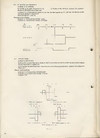
2 Tracks at the minimum access time between
5-3 Track Sensor Adjustment
a) INsert a CE diskette.
b) Continuously seek between andtracks of DFC222A specifications.
c) Adjust the track sensor assembly so that the step signal and track one are always on the
timing as shown in Figure 5-3.
Then secure with a screw.
Measuring ConditionsChannel 1-TP4 (0.2V/div) MODE-DUALChannel 2-TP8 (0.2V/div) Sweep-10ms/div
AStep Signal
TK Signal
2TK 1TK QTK 1TK 2TK
Direction J
5-4 Azimuth Check
a) Insert a CE diskette.
b) Move the head to Track 34 and check that the azimuth waveforms of the top and bottom headsare as described in Figure 5-4.
c) Exchange the head assembly if the azimuth of one of the top and bottom heads is not as shown in
Figure 5-4.
Measuring Conditions
Channel 1-TP1 (10mV/div) MODE-ADDChannel 2-TP2 (10mV/div) Sweep-1 ms/divTrigger—TP6
<\
L) Wher. a>d (negative")
v.. =- V,
Shows tiinuta
2"> Vher. a<d (positive)
Ymsz be c2c.abed
Shows misalignment by -IS'. Shows misalignment bv +13'
Head azimuth « 0°-18'.
Fig. 5-4
12

5-5 Index Burst Time Adjustment
a) Insert a CE diskette.
b) Move the head to Track 34 and check the index burst times of top and bottom heads. Adjust as
follows if the timing of one of the top or bottom heads is not as shown in Figure 5-3.
c) Move the index sensor assembly back and forth by slightly loosening the index sensor assembly
fix screws to adjust the index burst time.
d) Check the index burst times of the top and bottom heads.
e) Repeat from c) if adjustment has been unsuccessful.
Measuring Conditions
Channel 1-TP1 (10mV/div) MODE-ADDChannel 2-TP2 (10mV/div) Sweep-0.1 ms/div
Trigger- Edge Connector J2 8 pin. Slope ( ••)
I N D
Hea d Reading Output Si
( T P I - T ? 1 )
!00:£00jj s
270mV.
5-6 Level Check
a) Insert a blank diskette.
b) Move the head to Track 39 and write 2F by the top and bottom heads.
c) Check that the average output level of the top and bottom heads is more than
Perform the following if the output level is below the required standard.
d) Insert another blank diskette and reconfirm.
e) Check the spindle speed as described in 5-1.
f) Change the oscilloscope to the CHOP mode and check the TP1 and TP2 outputs. Exchange the
printed circuit board if one output is small or missing, even if the probes are normal.
g) Exchange the head assembly if no problems are encountered in d), e). and f) above.
Measuring Conditions
Channel 1-TP1 (10mV/div) MODE-ADDChannel 2-TP2 (10mV/div) Sweep-20ms/divTrigger—TP6
Head Reading Out Signal (TP1-TP2)
^%>wi&P* ^*=*hmji^
A A = 270 mV I" i n
13

5-7 Resolution Check
a) Insert a blank diskette.
b) Move the head to Track 39, write 1 F and 2F by the top and bottom heads, then measure theaverage output level.
c) The resolution is higher than 55%, and calculations shall be as follows:
2F output (mV)/1 F output (mV) x 1 00>55%Measuring Conditions
Channel 1-TP1 (10mV/div) MODE-ADDChannel 2-TP2 (10mV/div) Sweep-20ms/divTrigger—TP6
2F average output level
Resolution =1 F average output level
95% or less with TKO55% or more with TK39
5-8 Symmetry Check
a) Insert a blank diskette.
b) Move the head to track and write 1 F by the top and bottom heads.
Measuring ConditionsChannel 1-TP5 (0.1V/div) MODE--CH1Trigger—INT.CH1 Sweep-0.5ms/div
Slope(+)
T = 400 ns or less
(If you have individual spec, this item obey your spec.)
5-9 Write Protect Sensor Check
Load and unload a diskette and check that write protect sensing is definitely made using Brikon.
5-10 Head Cleaning
Check for excessive dust or oxidised magnetic iron powders on the load pad using such a dentist's
mirror. Clean the heads using a cloth that produces no flues or an applicator dipped in 91%isopropyl alcohol. Clean the heads carefully and remove accumulated dust and oxidised magneticiron powders. Wipe the head using a cloth that produces no flues.
14

FD-3 EXPLODED VIEWTHIS DRAWING REFERS TO ALL THOSE DESCRIBED IN THE TEXT
J§ -5
15

16

17

ELECTRICAL PARTS LIST
Decription Circuit Reference Part No.
Metal Oxide Resistors
0.22ohm/y2W R544, 545 1715840.22ohm/1W R547-550 1715850.33ohm/2W R504 1710721ohm/1W R415 17106947ohm/1W R520 17158656ohm/1W R541 17158756ohm/2W R511 171588100ohm/1W R407 171589470ohm/1W R428 1715901kohm/1W R506 1704062.2kohm/1W R513 1715914.7kohm/2W R802 17107622kohm/3W R512 17159282kohm/1W R509 171593
Fuse Resistors
1ohm/ 1/2W R427 17159410ohm/ 1AW R516 80925622ohm/ 1/2W R426 17159539ohm/ 1/4W R406 1715961kohm/ 1/4W R515 171597
Cement Resistors
5.6ohm/5W | R501 1422133
Ceramic Capacitors
680pF C540 14002132000pF/4kV C539 1704300.001 5uF/500V C524 1715980.0022uF/2kV C502-504 14002230.0056uF/500V C516, 520, 527 1715990.01uF/1kV C508 171600
Electrolytic Capacitors
10UF/25V C427 17160110uF/160V C429 171602150uF/400V C505 171603220uF/35V C435 20055330uF/35V C517 171604470uF/16V C522 14002481000UF/10V C425 1716051000uF/16V C530 14001581000uF/25V C521 1716063300uF/16V C529 1716073300uF/35V C525 171608
Metal Polycarbonate Capacitors
0.1uF/250V | C428 171609
Metal Plastic Capacitors
0.1uF/250VAC | C501 171610
Variable Resistors
VR201 Volume Rotary Gang500ohm-10kohm
171611
VR204 VRSF 500ohm 171612VR401 VRSF 500ohm 171613VR402 VR Rotary 30kohm 171614VR403 VRSF 10kohm 171615VR404 VRSF2kohm 171616VR405 VRSF 100kohm 171617VR501 VRSF 5KO 171618VR502-505, 507 VRSF 1kohm 171619
Switch
SW501 l Power On/Off Switch 171511
Circuit Reference Description Part No.
Coils & Transform ers
L201 CoreTridal L201 171557L401 Coil Linearity 171558L402 Coil Inductor 171559L501 Coil Line Filter AC 171502L502 Coil 171560L503 Coil 171504L506 Coil Core Tridal 171620L801 Filter Line 171561T401 Trans Horizontal Drive 171562T501 Transformer Switching 171563FB401 Flyback Transformer 171564
P.C. Boards
PCB001 MM0018A 171565PCB002 MS0053A 171566
Jack
Socket CRT 171567
Miscellaneous
CD201 Cord DIN 171568CD402 Cord Jumper 171569CD403 Cord Jumper 17lA||iCD404 Cord JumperCD502 Cord DIN 171571CD801 Cord Connector 171572DY401 DY 171573TH401 Thermistor 171574V801 Tube, Cathode Ray
340AXBWDN171575
Fuse Fuse 3.1 5A(T) 171621
PC-CMI.C.'s
IC101 I.C. OEC9001 1771477IC102 I.C. TC74HC02P 171622IC401 I.C. UPC1378H 170444IC402 LA7820 1400368IC501 STK7356IC502 L78M12 190062IC503 L78M05 190063IC601 STK7358 171479IC602 BA6993 171480IC603 LA6324 170112IC604 BA707 171481ICP501.502 ICP-N75 171075ICP503 PFR-315-F003 1714
171 &SICP601 ICP-N50
Transistors
Q101-103, 105- 2SC1815 170447113, 401, 601,602, 610-612,616, 618, 801-803Q401,402,603, 2SA1015 170453606,607,613,617Q403 2SD1426 171484Q404 2SC2271 170449Q604, 605 TLP580 171485Q608, 609, 615 2SD1207-T 170451Q614 2SB1134R 171486Q804-806 2SC3789 171487
- - .,.- - -.
18

ELECTRICAL PARTS LIST
Reference Description Part No.
Resistors
5.6ohm Fuse1kohm
R181R189-194 10061
Resistor Network
NR101NR102NR103NR104NR105NR801
4.7kohm x 7
1 kohm x 52.2kohm x 62.2kohm x 5
4.7kohm x 8Lkohm x 10
Ceramic Capacitors
47pF NPO0.1 uF
TC101
C805, 806C504-506, 802, 803
Trimmer 200pF Ceramic
Electrolytic Capacitors
47uF/16V ! C801
Crystals
X101X102X103
mX801
Crystal HC49U.843MCeramic Oscillator
Crystal DSVT30032KCrystal HC18RW24.0Crystal HC18RW28.636Ceramic Oscillator KBR-6.0M
Coils
Inductor Coil L101, 102
Jacks & Connectors
14 Pin DIL8 Pin DIL20 Pin DIL9 Pin D SKTMate N LockMate N LockSocket D SubDIN Cord 6 Way
J101, 102J1 03-1 20J121, 122J801CD101CD104CE101-103CD801
Semiconductors
Description
Diodes
DS442X-BTTLS134A LED
Reference No.
D101-104, 501, 502,801D503
171666171667171668171669171670171671
171672171058
171371
20027
171372171373171374171375171376171377
171404
170120170119170121171408171673171674171675171420
Part No.
1422117171403
IC's
MC1488P IC101 1713781489AP
•«r7406PIC102, 103 171379IC104 171380
DN74LS373 IC105, 122 170108INS8250N IC106 171381DN74LS240P IC107, 117 171382DN74LS244 IC108, 115, 121, 124 171383MBL8259A-2P IC109 171384DN74LS125P IC110 171385SED9420CAC IC111 171034UPD765AC-2 IC112 40018DN74LS174P IC113 171387UPD8253C-5 IC114 171388DN74LS14P IC116 171389AMS40040 IC118 171391MBL8086-2P IC120 171392DN74LS245P IC123 171393AMS40039 IC125 171577AMS40041 IC126 171394AMS40045 IC127 171395TC74HCUD4P IC128 40008/AAMS40043 IC129 171396UPD8237AC-5 IC130 171397UPD4126C-15 IC131, 133 171398AMS40044 IC132 171578MC146818P IC134 171399MN41256-15 IC135-152 171400LA4140 IC401 170111
AMS40042 IC801 171401TC74HC14P IC802 171033
Description Circuit Reference Part No.
Transistors
2SC1815Y2SA1015YKTC2120
Q101, 102, 105Q103, 104, 106, 107Q1 08-1 13
170447170453170113
Switches
SW801 Switch Key Board 171409
Variable Resistors
VR401 Volume Control CPU Unit 171579
PCB Assy's
PCB101PCB102
PCB801
CPU PCB MC0032BLED PCB MC0033BPart of PCB101Keyboard PCB MK002A
171410
171412
PC-MM
Intergrated Circuits
IC201IC401IC402IC501IC502IC503IC504
TC74HC04 40008/AAN5753 151040UPC1031H2 171546STK7356 171478BA6993 171480LA6324 170112BA707 171481
502 ICP-N50 171547
Transistors
Q201-203, 205,401,506, 511, 512Q204, 520Q402Q501, 502, 514,
518, 519Q503, 507, 508,517Q504, 505Q507Q509, 510, 516Q513, 515Q801
2SC1815
2SA10152SD11592SC536
2SA608
TLP5802SC22292SD12072SB1134R2SC2229
Diodes
D207D208, 401,402,410,512, 513, 517521, 524, 525D403D404, 405, 407D406D408D409D501-504D505D506D507D508-510D511, 526, 527D514D515D516D517D520, 801D522D523D528-531
D.Z. MTZ5. 1 BT-77D. ISS231T-77
C. 11E2TA1 Diode Silicon
D.10ELS4 Diode Rectifier
D.11E1TA1 Diode Silicon
D.Z. GZA6.2Y Diode ZenerD.KDS1555 Diode Silicon
D.20E10FA13D.Z. GZB18BD.DFC15L-KC5D.Z. GZB9.1BD.DFH10G-KB4D.Z. GZA18YBTD.30DF2DSF 10BD.F5KQ60D.F10PO4QD.DS442X-BTD.Z. MTZ5.1BTD.Z. MTZ5.6BTD.KDS1555
Carbon Film Resistors
330ohm/ 1/4W R572470ohm/ 1AW R57110kohm/ 1/4W R57375ohm/V2W R238-243
170114
170453170623150350
920113
171548170624170451171486170624
1422112171582
171549171550171551171552800222171048171553171491171493171492171554171555171556171496171497
14221171422112171499810332
100441004810085
151583
19

ELECTRICAL PARTS LIST
Circuit Reference Description Part No.
Diodes
D101-105D106-115, 401-405, 407-409,505, 608, 609,613, 616-620D406, 412, 413,610D410D411D501-D506,D507,606D508,D510D511D601D607D611D612D614D615
504603509, 604-
602
MTZ6.8BT-77ISS132T-77
DFD05G
D.Z.MTZ11BTC.BB4-FC20E10FFA13DFC15L-KC5DFH10G-KB4
GZB9.1B30DF6-FCSR-2MGZB18BGZA18YF5KQ60F10PO4QMTZ5.1BT-77MTZ5.6BT-77
Carbon Film Resistors
75ohm|R1 54-1 58
Metal Oxide Resistors
0.22ohm/y2W0.33ohm/2W1ohm/3W4.7ohm/3W15ohm/2W47ohm/1W56ohm/1W68ohm/2W100ohm/2W1kohm/1W2.2kohm/1W3.3kohm/1W3.9kohm/1W4.7kohm/2W5.6kohm/2W22kohm/3W33kohm/2W82kohm/1W
R641-646R604R502R438R511R624R737R512R507, 612R610R613R504R503R434R805-807R609R508R607
Fuse Resistors
0.82ohm/1W R4421ohm/y2W R4438.2ohm/1/4W R437lOohm/'AW R510100ohm/ 1/4W R412100ohm/ 1/2W R444470ohm/ 1/2W R5091 kohm/ViW R614
616
Cement Resistors
5.6ohm/5W R501, 601
Ceramic Capacitors
100pF C442470pF/2kV C429820pF/2kV C5230.001 uF/2kV C8010.001 5uF/500V C6200.001 5uF/2kV C511, 514,8070.0022uF/2kV C502, 6040.0056uF/500V C612, 617
171488171489
171490
1716231422116170848171491171492
171493171494
1400122171495171624171496171497171498171499
10029
171625171072171077171626171627171628171629171630171631170406171632171633170407171634171635171636171637171638
1422141171639170404809256171640
1400183171641171642
1422138
14221441400224171643
1422147171644171645
1400223171646
Description Circuit Reference Part No.
Polyester Capacitors
0.1ur/100V | C404 |1400237Electrolytic Capacitors
1UF/250V C440 17164710uF/100V C509 17164822uF/250V C436 171649150uF/400V C506, 601 171650220uF/160V C515 171651330uF/25V C613 171652470uF/35V C516 1716531000uF/16V C623 14221581000uF/35V C437 15221592200uF/35V C408 14221603300UF/16V C621.622 1716543300uF/35V C618 171655Metal Polypropylene Capacitors
0.0082 uF/1.6kV C430 1716560.32MF/200V C433 171657Metal Plastic Capacitors ^
0.1uF/250VAC | C501|17l||p
Coils & Transformers
L401 Coil Line^.ty 171500L402 Coil RX-9P-472K 171501L501 Coil Line Filter AC PLA1022C 171502L502 Coil Degauss 171503L601 Coil 171504L80 1-804 Coil ELO606RA-101K 171505T401 Trans, Horizontal Drive 171506T501 Tranformer, Switching 171507T601 Transformer, Switching 171508FB401 Transformer Flyback 171509Switches
SW401 I Switch Slide 171510SW501 | Switch Push 171511
P.C. Boards
PCBO0
1
PCB MM0019A Monitor Main 171512PCB002 PCB MS0054A CRT Socket/ 171513
Colour Drive
Jacks
J801 Socket, CRT 171514JC801 Socket Cover CRT 171
l<WMiscellaneous
CD101 Cord DIN 14 Pin 171519CD601 Cord DIN 8 Pin 171522F501 FuseS506 3.15A(T) 171531TH501 Degauss Element 171533V801 Tube, Cathode Ray
M34EAQ1 0X-AT1 460/90171534
ICP501, 502 ICP-N75 171057ICP503 PRF-315-F003 171483ICP601 ICP-N50 171547
Variable Resistors
VR101, 103 VRSF 1KOhm 171691VR102 VR Rotary 500ohm-500ohm 171692VR104 VRSF2KOhm 171616VR401 VR Rotary 200Kohm 171693VR402 VRSF5Kohm 171694VR403 VRSF5Kohm 171695VR404 VRSF500ohm 171612VR601 VRSF5Kohm 171618VR602-604, 606 VRSF 1Kohm 171619VR801 VRSF 5Kohm Red 171696VR802 VRSF 5Kohm Green 171697VR803 VRSF5Kohm Blue 171698VR804 VRSF 500ohm Red 171699VR805 VRSF 500ohm Blue 171700
20

CABINET DIAGRAM EXPLODED VIEW
21

CPU P.C.B. ASSEMBLY COI
MC0033BELC4762 94V-0
if S-ss is n/ 38
sit? otoa
22

BLY COMPONENT SIDE
1HHH1
K|::;:5| 32B 6LC*762 94V-0
23

CABINET PARTS LISTRef. Description Part No.
1 Cabinet Top 1713502 Lid Expansion PCB 1713523 Plate Earth CPU 1713644 Cabinet Front Assembly SD 1714505 CPU PCB 1714106 Cabinet Bottom 1713517 Lid, Jack 1713538 Frame FDD SD 1713658a Frame FDD A IN DD 1713669 Screw Cap 171363
10 Plate Spring Battery 17136711 Terminal Battery 17136812 Cabinet Front Assembly 17135913 Plate Shield Top 17168914 Plate Shield Bottom 17169015 F.D. Drive (A&B) 17157617 Knob Volume 17136218 Speaker 17137019 Fan HD Unit 17166521 Top Cabinet Keyboard 17135422 Switch Key Board 17140923 Keyboard PCB 17141224 Cabinet Bottom Assembly 17135525 Stand Keyboard 17135826 Washer 17165927 Cord 6 Pin DIN/Keyboard 171420
Cabinet Front Assembly HD10 171660Cabinet Front Assembly HD20 171661HD10 Kit Assembly 171662HD20 Kit Assembly 171663Mouse MS-2 171664Leg Rubber 171357Leg Rubber 171356Plate Brand (Keyboard) 171360Plate Brand (C.P. Unit) 171361
EXPLODED VIEW C.P. UNIT
24

HARD DISC INSTALLATION INSTRUCTIONS
Applies to both ten and twenty megabyte versions.
1. Turn on machine.
2. Insert disc 1 (the red disc) and press a key.
3. Type fdisk (RETURN)
4. At each prompt press the RETURN key (another three times).
5. The A> will now appear so now type format c:/s (RETURN).
6. Now push the Y key (RETURN).
7. The hard disc will now begin to format, if you have a 1 0Mb machine then it will cc in. u_ t ) 305cylinders. If you have a 20Mb machine then 610 cylinders will be counted.
8. Once this is done, take out disc 1 and insert disc 5 (the maroon disc).
9. Nowtypeconfig(RETURN).Thisprocedurewillcopyallfivediscs(order5,1,2,3,4)ontc h< had &•
Once finished the screen willshowsomeinformationaboutthesizeofthediscandthenumb., f nd
directories present.
1 0. To now use the hard disc remove the floppy disc from the driveand store in a safe place wi efour discs then restart the computer by pushing Alt Ctrl and Del.
1 1
.
After a short while the AMSTRAD PC info will come up and tell you when the machine was la ui
and then after a little longer the screen will clear and will display this message,
F1=DOSPLUS.SYSF2=DOS.SYS
Select operating system:
If you choose F1 then DOS Plus and Gem will be booted, or if you press F2 then MS-DOS will be booted.
25

ALIGNMENT INSTRUCTIONS FOR PC-CM
Equipment required: Digital Multimeter; Dummy Load; 0.82ohm/30W, D.B.O.Scope; Odometer (Teal Time Meter),
Diagnostic Disc/Tool.
Step FUNCTION SIGNAL IN SIGNAL OUT METHOD REMARKS
1. To Set +5V. Power supply. Test Point A Adjust VR604 to read 5.10V ±0 02V. 1) Refer to Fig. 1.
2) Prevent short circuit when pulling
the PCB forward.
2. To Set + 12V. Power supply. Test Point B. Adjust VR603 to read 12 15V +0.02V. 1) Refer to Fig. 1.
2) Prevent short circuit when pulling
the PCB forward.
3. To Set -5V. Power supply. Test Point C. Adjust VR601 to read 5V ±0.05V. 1) Refer to Fig. 1.
2) Prevent short circuit when pulling
the PCB forward.
4. To set -1 2V. Power supply. Test point D. Adjust VR602 to read 12.0V ±0.05V. 1) Refer to Fig. 1.
2) Prevent short circuit when pulling
the PCB forward.
5. To set protect
adjustment.
Power supply. Pin 11 of 14 Pin DIN Plug. Adjust VR606 to read 4.5A on the
ammeter in series with dummy load.
1) Refer to Fig. 1.
2) Prevent short circuit when pulling
the PCB forward.
6. V. Size setting. Load diagnostics in PC1512. Monitor screen. Adjust VR404 so the border is
1 2mm ±3mm all around.
Set optimum Brightness &Contrast setting.
7. Sub Brightness Control. Load Diagnostics in PC1512. Monitor Screen. Set VR 102-2 to max. adjustmentVR101 so the grey level wave form
is 27% when initial white level is
100% against black scope Q302collector
1) Refer to Fig. 2.
8. Sub Contrast Control. Load Diagnostics in PC1512. Monitor Screen. Select Colour Bar Chart. Set Bright
Control to VR102-2 max. andVR1 02-1 to min. Adjust VR1 03 to set
proper intensity level.
9. Sub H. Hold Control. From IC402 Pin 4. Scope Pin 4 of IC402. Set VR403 to Mid position.
Adjust VR402 to read
Frequency 15.625kHz. mNOTE
It is very important to observ the isolated power supply area. Any measurements within the power supply circuit should be
carried with reference to top point of C505 in order to keep the chopper circuit oscillating.
MAJOR COMPONENTS LOCATION GUIDE
VR403H.HOLD
00 VR402SUBH.H0LD
:^s>
oj—
®
„VR601(1-5VADJ.
VR60312VADJ.Q)VR604 .—
.
5VADJ.LJ
IC101
VR602-12V ADJ.
QVR60612V
QVR101IGRAY
PROTECT
,—iVR103LJsub
CONT.
Qv.size
IC402
r-GRAY
-f:phnrf^uyuuuiiNTWurrtJ
Fig. 2.
Fig. 1.
26

ALIGNMENT INSTRUCTIONS FOR PC-MMEquipment required: Digital Multimeter; Dummy Load; 0.82ohm/30W D.B.O.Scope; Diagnostic Disc/Tool.
Step FUNCTION SIGNAL IN SIGNAL OUT METHOD REMARKS1. To Set +5V. Power Supply. Test Point A. Adjust VR505 to read 5.10V ±0.02V. 1) Refer to Fig. 3.
2) Prevent short circuit when pulling
the PCB forward.
2 To set+12V Power Supply. Test Point B. Adjust VR504 to read 1 2.1 5V ±0.02V. 1) Refer to Fig. 3.
2) Prevent short circuit when pulling
the PCB forward.
3. To Set -5V. Power Supply. Test Point C. Adjust VR501 to read 5V ±0.05V. 1) Refer to Fig. 3.
2) Prevent short circuit when pulling
the PCB forward.
4. To Set -12V. Power Supply. Test Point D. Adjust VR502 to read 1 2.0V ±0.05V. 1) Refer to Fig. 3.
2) Prevent short circuit when pulling
the PCB forward.
5. To set protect
adjustment.
Power Supply. Pin 11 of 14 Pin DIN Plug. Adjust VR507 to read 4.5A on the
ammeter in series with dummy load.
1) Refer to Fig. 3.
2) Prevent short circuit when pulling
the PCB forward.
6. To set +1 2V tor monitor. Power Supply. Test Point B. Adjust VR503 to read 12.0V ±0.05V. 1) Refer to Fig. 3.
2) Prevent short circuit when pulling
the PCB forward.
7. Centering the Screen. Screen On. Observe Screen. Adjust DY and 4 Pole Magnets to
get 12mm ±3mm Border.1| Refer to Fig. 3.
8. V. Size Cont. Screen On. Observe Screen. Adjust VR403 to get Circle. 1) Refer to Fig. 4.
9. V. Linearity Adjustment. Screen On. Observe Screen. Adjust VR404 to get E-F Equal. 1) Refer to Fig. 4.
10. Cut Off Adjustment. Screen On. Observe Screen. Set VR20M/2 to max. adjustmentVR405 so the. black on the screenwill not be bright.
1) Refer to Fig. 5.
11. Sub Contrastadjustment.
Screen On Observe Screen. Set VR201-2 to max. and VR20M to
min. Adjust VR203 so Y-4 is slightly
bright.
1) Refer to Fig. 5.
->
P2)VR502
QVR507^12V
PROTECT
12VADJ.
DM.r>iVR504
'12VADJ.
VR401H.HOLD
DVR50312VM0N.ADJ
IC503
\ymDJ.
uQVR405
CUT OFF|0|
<D)
aVR404V.LINE
aVR403V.SIZE
IC201
I FB401]
A
Bv?ND
b^y Oc
Fig. 4.
Fig. 5.
Fig. 3.
ALIGNMENT INSTRUCTIONS FOR PC1512Equipment required: Digital Multimeter; Dummy Load; 0.82ohm/30W, D.B.O.Scope; Diagnostic Disc/Tool.
Step FUNCTION SIGNAL IN SIGNAL OUT METHOD REMARKSSet RTC X-103 Connect Odometer to
Pin 21 IC134.Set Odometer to 0.2sec/Day. Adjust it toDo this adjustment only if the real
read 0.00 with TC101. I timeclock chil is changed.
27

C0COCOCD(O(O(OC0C0T"-C0oic\Jh-coT-c\jcomtD
< m
2 ;g
.£ .£ t <5
- CD 5 fi 1> <» t OT
:£ Eot3S£.E.-* 5 2 re* « a^
) — U_ CD O 0- Q. (/) 5
28

CABINET PARTS LIST PC-MM
Sym Description Part No.
51 Front Cabinet Assembly 17154052 Holder PCB (R) 17154253 Holder PCB (L) 17154154 Cabinet Back 17154555 CRT 340AXBWDN 17157556 CRT Socket 17156757 Metal Washer 17158058 CRT Spacer 17158159 Stand Bottom 17146160 Stand Top & Spacer 17146361 Holder Stand 17146262 Frame, Bottom 17154363 Button Push 17146964 Knob Volume 17136265 8 Pin DIN Cord 17152266 14 Pin DIN Cord 17151943 Screw Tap Tite
oQ.
<cc
o<QI-UJ
zGO
<o
29

CH
30

CHASSIS SCHEMATIC DIAGRAM
>
>
-f=CEE
-€
<< BA3
^C NIOW 55
PDSTBOCSTBNPSTATNPCRB
CKI4RESETALE[ORDYNMEMWNMEMRNIOWNIOR
BAI9BA1BBAI7BAtG
BAD 1
5
BAD 1
4
BAD I 3BAD 12BAD I I
BAD1QBAD9BADB
BA7BAGBASBA4BA3BA2BAtBAO
NRTCDSr«TCRWRTCAS
AMS VDUGATEARRAYICI2B
40041
z z z
CHAR7CHARGCHARSCHAR4CHAR3CHAR2CHARICHARO
7SD7tfSDG
VSD5VSD4
VS03VSD2VSD1
NVRASNVCASNVMWE
NVOTOEVSC
VMA7VMAGVMASVMA4VMA3VMA2VMA1VMAO
"i
rTr
I CI 27AMSROM40045
o - cm mo aL/if/l C/i i/i
DT/QESC DUAL PORT
D-RAMLCI 31
A7 25GKAG 4I2G4-1SAS
1 lD 01 CD CM I" 81
wy
in vxsunRASCASWB7 WESOEDT/OESC
DUAL PORT0-RAMIC133
A" 25GKAGA5 412G4-1SA4A3
N w w H
I I I I
12 3
CAUTION SINCE THESE PARTS MARKED BY ZJJ\ ARECRITICAL FOR SAFETY USE ONESDESCRIBED ON PARTS LIST ONLY.
ATTENTION U.ES PIECES REPAREES PAR UN & ETANTDANGEREUSES AN POINT DE VUE SECURITE•J'UTILISER QUE CELLES DECRITESDANS LA NOMENCLATURE DES PIECES-
THIS SCHEMATIC DIAGRAM IS THE 1_ATEST AT THE TIMEOF PRINTING AND SUBJECT TO CHANGE WITHOUT NOTICE.
31

CHi
: :i303237A-5 DMA
1 Z O _1 IQj^EISIir
till uluii-hC X * o oJ U U U UJ U LJi < < en a. a. tz2 O Q Q H Q Q
2 d|3 2
i ..!;...
T
t:
I C 1 093259A-2 PIC
* IS £ IB
$ 'f-V
:ci 148253-5 PIT
3 < 3 ^SOOli^lIO
d m £ :
?ajS tMD'S;
32

CHASSIS SCHEMATIC DIAGRAM
A A A A
ft vA At T
>
:A
T
A A A A A Af T t f t v
sA;T
A A
I BA1E
7 : C II 5 At7
9 id :5 A16
L5244
211
BAD IS 3
D ^
A ' 5c
SAD 14 : 5 1 A. 4 =
r BAD!
3
"
6 *,
AI3r BAD12 a 3 AI2 I[ BADI
1
12 12 AM3ADI0 .:
s 'a
15 A10C
fBAD9 1 7 IG \ A3 <
, BADS IS 19 * AS I
ICI22l| Yi 74LS373
BA7 ; |
r^
9 A7' BAG 8 '2 46' BAG 13 ? AG' BA4 6 14 A4
1, PA3 15 / > 5 A33A2 4 l> 16 A2
s BA1 3 Al
L BAQ 2 18 AO
[ CI 21
: ^X
< BADI
1
TONRIOG 4K7
-1—
,A n
244 OUTPUT BUFFERPACKAGE ENABLES
A20A2!
A22A23
A24A2GA2GA27A28
A03A04
IRQ2' IRQ3' 1RQ4 *
( [RQS
, iRQG I
. IR07
NDACKO
LCI 15J-5244
. P^ C
NDACK
1
4^ IG
NDACK2c
' NDACK3
' DRQ1, DRQ2 £
DRQ3
BQ2B28B20
B27
At I
B04B2GB24B23B22
*5V
1 o
ov
-GV
-12V
AOI
AID
B09
B03
B23
B31
BOG
B07 '
EXPANSHIONBUS5QWAY O.l"EDGE CONNCE101 -103
33

KEYBOARD SCHEMATIC DIAGRAM AND P.C.B. LAYOUT
Yl
Y2
Y3
(5
Y6
Y9
X8
F8CLEFT)
o
X
V
N<?
PRTSCkR
2i
X8
F7
Z
c
M
ilGHT)
o
END
3PGDN
DEI
X7
XG
FG
A
D
G
J
Q
5
INS
XG
X5
FG
CTR1
G
F
H
K
#
CAPS
LOOK
X5
F4
Q
G
T
U
[
7HOME
9PGUP
(SPACE)
X3
FG
R
Y
P
ALT
X3
X2
F2
3
5
7
(
9
SCROLL
LOCK
F10
X2
F
ESC
5?
2
X
)
o
NUM
LOCK
ENTER
FGXI
Y2
Y3
YS
ys
r9
.
->--^-t>
-2->
KEYGOARDSW80
1
ESU-243S
34

RADS FDRCURLY CABLETERMINATION
J801JOYSTICK9-WAYD-TYPE PLUG
35

KEYBOARD EXPLODED DIAGRAM
36

CHASSIS SCHEMATIC C
1AAJU
AC IN 24DV50HZ
4
CAUTION SINCE THESE; PARTS MARKED BY A AR:
CRITICAL FOR SAFETY USE ONESDESCRIBED ON PARTS' LI ST ONLY,
ATTENTION ,_ES PIECES REPAREE
DANGEREUSES AN PO
N'UTILISER QUE CEI
DANS LA NOMENCLATl

IATIC DIAGRAM PC-MM
TO MONITOR-;r+12,
IECES REPAREES PAR UN A ETAN*3EUSES AN POINT DE VUE-SECURITE.ISER QUE CELLES DECRITES.A NOMENCLATURE DES PIECES.
NOTE THIS SCHEMATIC DIAGRAM IS THE LATEST AT THE TIME
OF PRINTING AND SUBJECT TO CHANGE WITHOUT NOTICE
37

CHASSIS SCHEMATII
38

HEMATIC DIAGRAM
1_ k h rii^n. hh h fa
1 53- 1 G
I
64 K DRAM
OPTION'
RAS
CAS,J L
Vol
fl 1
a - oj m
1"1
IC162-170'3 X 64 K DRAM
OPTION <
Lc WE
^c RAS
CAS
I75E
A \ \ \
"1
I C 1 32AMSROM40044
AI2
^Ca13
X CK5
QO Q1 Q2 Q3 Q4 G5 QE Q7
I 01 29A"; AMSA4 ROMA3 40043A2
ROM SIZE SELECT OPTION LINK
FLTRKO 33
f FRSTEP 37
T RWSEEK 33
\ WDIN 30
t =>S1 31
f -50 32
L rjORQ 14
1 DINT
L NDACK'"r
I DRESET,
!
CK4. L J9
.••?
DRIVE 5ELECT
DRIVE SELECT 1
MOTOR ON
WRITE DATA
DIRECTION TN/t
SIDE SELECT
NIOR 2 .
NIOW 3 -
NFDCS » -
BAO 5
BADIS 13
BAD14 12
% BAD 13
BADI2 10
-c.BAD1 I 9
k BAD 10 BBAD9 ?
k BAD8 S
CD 102
FDD 34 WAY CONN
CD101DRIVE 1
DOWER
CD 104DRIVE 2 POWER
CP105DRIVE 3 POWER
ATTENTION l-LS PIECES REPAREES PAR UN ^ ETANTDANGEREUSES AN POINT DE VUE SECURITENUTILISER QUE CELLES DECRITESDANS LA NOMENCLATURE DES PIECES.
CAUTION^ SINCE THESE PARTS MARKED BY ^ ARECRITICAL FOR SAFETY USE ONESDESCRIBED ON PARTS LIST ONLY.
NOTE: THIS SCHEMATIC DIAGRAM [S THE LATEST AT THE TIME
OF PRINTING AND SUBJECT TO CHANGE WITHOUT NOTICE.

CHASSIS SCHEMi
DI02 DID3DS442XFA5 DS442XFAS
r—r—=r^-
51?5f^
G°L
'
ICI34318 RTC
— CM l/l Uuuu.cn1/1 C/l X \Ulj —
T
t r-> en
U
L.1 ID [N CO cn _ —
\ \\v///;BAD8- BAD I 5 )
DRI54ISK V i
v
IN
JD50'POWERDIN
PIN SOCKET
//_
3
J
12.4.10)-
"9"
ir~i
—
o~l 1t;~<->
3? s a-.T_""Taos
-4—
•
i 1 1(
POWER LEDDS03
TLS134A
> * bl X
^-sv
-12VDE02
DS44'2X-BTlg--
LES PIECES REPAREES PAR UN A ETANTDANGEREUSES AN POINT DE VUE SECURITEN'UTILISER QUE CELLES DECRITESDANS LA NOMENCLATURE DES PIECES.
CAUTION SINCE THESE PARTS MARKED BY A ARE
CRITICAL FOR SAFETY USE ONES
DESCRIBED ON PARTS LIST ONLY.

CHEMATIC DIAGRAM
*
"
IP ££ u
< Z
m
CD
\\
tEICID574LS373
51 NFM01
4K7
3ADI5 9r" BAD 14 \2-^ BAD!
3
7-~ BADI2 14
*C BAD1 ! 5-_ BAD! 16
-^ 3AD9L_ BAD8
8
:B
<3
^«^
n
-o I I BUSY
-O 10 ACK-O 12 PE-o 13 SLCT-O 15 ERROR
m |-o 21 GND) 22 GNDI 23 GND
J » o 24 GNDP-P l—O 25 GND
JD1Q2PRINTER25 WAVD-SUB CONN.
JP101SERIAL PORT
2S WAY
D-SUB CONN.
THIS SCHEMATIC DIAGRAM IS THE LATEST AT THE TIME
OF PRINTING AND SUBJECT TO CHANGE WITHOUT NOTICE.
39

CHASSIS SCHEMATIC DIAGRAH
4,5V P-P (HI 150V P-p (HI 3.9V P-P
IC20I VOLTAGE
d 0.4 U 3.3 (pi) O.S'
? 4.7 -
;
2.B fe) 3.3 O.S (Q) 1 .9
2 3.9 O.0l|(s> 0.8 • 3.3 *\^
FROM 12V <+B
CAUTION^ SINCE THESE PARTS MARKED BY A ARECRITICAL FOR SAFETY USE ONESDESCRIBED ON PASTS LIST ONLY.
ATTENTION i_LS PIECES REPAREES PAR UN A ETANTDANGEREUSES AN POINT DE VUE SECURITEM UTILISER QUE CELLES DECRITESDANS LA NOMENCLATURE DES PIECES.
'ic :e rnis schema
CF orintING
40

IAGRAM PC-MM MONITOR
> 1 1J
8 4.1 V P-P (V) 9 12 V P-P (V)
CD4031 22G04
J=
% i1 A'
r r
DY401 Q27101 1403
CD4D2i 22G02
SAP -
3
i^
=C3001"'GO i 8
*
AMO(J I TOR
DISPLAY TUBEV80I
340AXBWDN
THIS SCHEMATIC DIAGRAM IS THE LATEST AT THE TIME
CF PRINTING AND SUBJECT TC CHANGE WITHOUT NOTICE, 1-4821

~\ m-
CHASSIS SCHEMATIC D1AGR
!. 620V P-P
LbC2C29Y14CCI 7
AC IN 240V SOFZ7FEE r
I 20 Lb3DCC9
IN J.S PIECES REPAREES PAR UN /]\ E TANT
DANGEREUSES AN POINT DE VJE SECURITE
N'UTILISER QUE CELLES DECRITES
DANS LA NOMENCLATURE DES PIECES.
CAUTION SINCE THESE PARTS MARKED BY A ARE
CRITICAL TOR SAFETY USE ONES
DESCRIBED CN PARTS LIST ONLY.

HC DIAGRAM PC-CM POWER SUPPLY
-SV >J>
GNO rn-
END 55
!2V -
CD5028GE8900I
GN3ENDgndF:-svg+5V
—PJ
41

PC-MM MAIN P.C.B. CO
X
: O
PTH). I 1 CP801
H xpc
R224*
R227
fax ^|
.
raw ^J^G 8 ,S
-R233 .r04! § « a
pjQ? MSlfli xpc~^*}
*«°' I 1PTN0 -Z70306 n
i R231
'ft
R228
0805 1*^
oca
C405
JJISIg R221
^g'S R2I4 ^7 R2 12
« 1,
i T I C414
^5fi6
2
_ o;*i
S !
!§'
C408H(-
§ C4H
C412
i
si 1
3 ffi
~—" ^ O C5,9
i-fl±
^UUO R42' C426 <3
IT 3.I5A|1
' F50Icsos
cr\J3
If3
SW501
f 3 BLUE
rem
CSCB
—W—
•
0KB,
K04H «J
42

».C.B. COMPONENT LAYOUT
XPC-FR-11V-0
MJ XPC-FR-1Z7030S 1V-0
BS29
-Sr0619 osn
W? SI 31
s. RS32 — •*B-lg (J
jB-i§J8- -SSK —"i, •*
. .w'l n - m
iT
o

PC-CM MAIN P.C.B. COMPONENT LAYOUT
bright! 5 3 2VRI04 XB a jj*
"
R
C622
^i|
i§| ||
T | » v* R1&
\i
"mo:
VR102-I
)UT
X 1 3) »
JO Ml — It !
C4I8R41S —4t—
C409
Ift
C423 'S HHJ I f^' 1
I |o, n? C441 M-'l ft
R422 '
n I o n -L1* -r
-I w I
R413 I I
|1212 Si 2
I TSTS" :
3 T^
TJtotf
glpspll R;29^' *.-«*-*yBF& R4I8C402
i:ffljj
PTN0.Z70304
5
gf^jzT
i(TO£904
/.fiND
-HI— .
pB co t
-<
1 0}
g co cog
i, L804;
'-> W 1
CRT P.C.B. COLOUR MONITOR
43

SCHEMATIC DIAGRAM
£e—><
44

)IAGRAM FD-3CPU
AT
XTAL1
f TC2E
TC2A
TC1B
TC1A
— t~ CD Ullj 3 < Z CL Wa < a u u £- 'J CE S f- —tn — 3 3 to oXXX X
3rx1ht
~T VTl. o*
52 x**— •_> 5-oin (J £*— h Z—
"- 3.
j_C=JjJ Goo UJt/1
xai LJf-ZUJ2 K3^)3LJ — as to
ZtO era.— 3


![Spectrophotometer CM-700d/600dCatalog] CM-700d.pdf · 2020. 5. 13. · (w/ plate) ø3 mm CM-A181 ø3 mm CM-A179 (w/ plate) AC Adapter CM-700d/600d Hard Case CM-A176 * For storage](https://static.documents.pub/doc/80x56/60e02953f3fabb7bd37c0eb3/spectrophotometer-cm-700d-catalog-cm-700dpdf-2020-5-13-w-plate-3.jpg)


