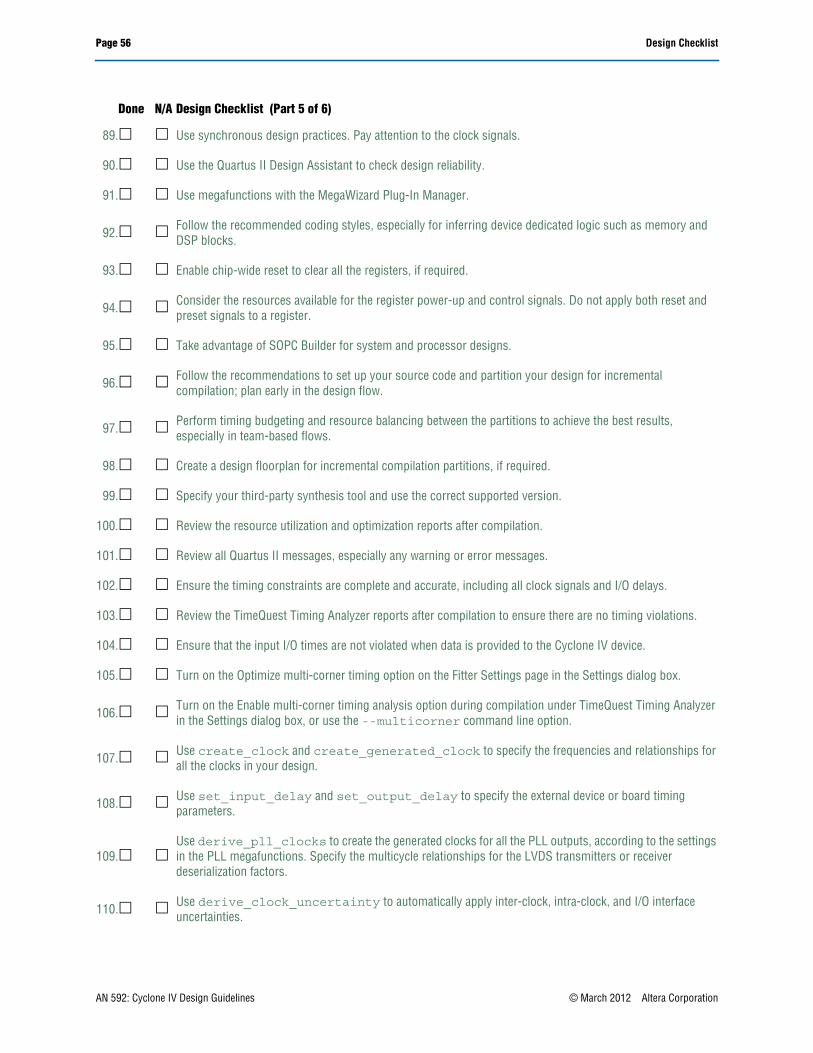
This application note provides an easy-to-use set of guidelines and a list of factors toconsider in Cyclone® IV designs. Altera recommends following the guidelines listedin this application note throughout the design process. Altera® Cyclone IV devicesoffer a rich combination of logic, memory, and digital signal processing (DSP) with thelowest power. Cyclone IV devices are ideally suited for cost-sensitive, high-volumeapplications, including displays, wireless infrastructure equipment, industrialEthernet, broadcast converters, and chip-to-chip bridging. Planning the FPGA andsystem early in the design process is crucial to your success.
This application note describes the Cyclone IV device architecture, as well as aspectsof the Quartus® II software and third-party tools that you can use in your design. Itdoes not include all the details about the product. It also refers to otherdocumentation where you can find detailed specifications, device featuredescriptions, and additional guidelines.
The guidelines presented in this application note can improve productivity and avoidcommon design pitfalls. Table 1 describes the various stages of the design flow in theorder that each stage is typically performed.
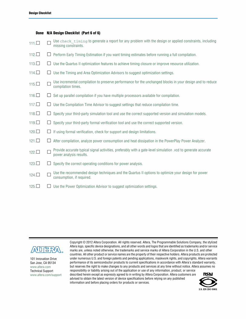
1 To help verify that you have followed the guidelines described in this applicationnote, refer to the “Design Checklist” on page 52.
f For more information about the Cyclone IV device architecture, refer to theLiterature: Cyclone IV Devices section of the Altera website. For the latest knownissues related to Cyclone IV devices, refer to the Knowledge Database.
Table 1. Summary of Design Flow Stages and Guideline Topics
Stages of Design Flow Guideline Topics
“System Specification” on page 2 Planning design specifications and IP selection
Early power estimation, planning configuration scheme, and planning for on-chipdebugging
“Pin Connection Considerations forBoard Design” on page 14
Power-up, power pins, PLL connections, decoupling capacitors, configurationpins, signal integrity, and board-level verification
“I/O and Clock Planning” on page 23 Pin assignments, early pin planning, I/O features and connections, memoryinterfaces, clock and PLL selection, and simultaneous switching noise (SSN)
“Design Entry” on page 35 Coding styles and design recommendations, SOPC Builder, and planning forhierarchical or team-based design
“Design Implementation, Analysis,Optimization, and Verification” onpage 42
Synthesis tool, device utilization, messages, timing constraints and analysis, areaand timing optimization, compilation time, verification, and power analysis andoptimization
System SpecificationIn systems that contain a Cyclone IV device, the FPGA plays a large role in the overallsystem and affects the rest of the system design. You must start the design process bycreating detailed design specifications for the system and FPGA and determining theFPGA input and output interfaces to the rest of the system.
Creating Design SpecificationsBefore you create your logic design or complete your system design, detailed designspecifications should define the system, specify the I/O interfaces for the FPGA,identify the different clock domains, and include a block diagram of basic designfunctions. For suggestions about including intellectual property (IP) blocks, refer to“IP Selection”. Taking the time to create these specifications helps to improve designefficiency.
Create a functional verification plan to ensure your team knows how to verify thesystem. Creating a test plan at this stage also helps you design for testability andmanufacturability. You may need the ability to validate all the design interfaces. Forexample, if you want to perform built-in-self-test functions to drive the interfaces, youcan use an UART interface with a Nios® II processor inside the FPGA device. Forguidelines related to analyzing and debugging the device after it is in the system, referto “Planning for On-Chip Debugging” on page 12.
If your design includes multiple designers, consider a common design directorystructure. This eases the design integration stages. For more information aboutteam-based designs, refer to “Planning for Hierarchical and Team-Based Design” onpage 40.
IP SelectionAltera and its third-party intellectual property partners offer a large selection ofoff-the-shelf IP cores optimized for Altera devices. You can easily implement theseparameterized blocks of IP in your design, reducing your system implementation andverification time, and allowing you to concentrate on adding proprietary value.
IP selection often affects system design, especially if the FPGA interfaces with otherdevices in the system. Consider which I/O interfaces or other blocks in your systemdesign can be implemented using IP cores and plan to incorporate these cores in yourFPGA design.
1. Create detailed design specifications and a test plan, if appropriate.
2. Plan clock domains, clock resources, and I/O interfaces early with a block diagram.
The OpenCore Plus feature available for many IP cores allows you to program theFPGA to verify your design in the hardware before you purchase the IP license. Theevaluation supports an untethered mode, where the design runs for a limited time, ora tethered mode. The tethered mode requires an Altera serial JTAG cable connectedbetween the JTAG port on your board and a host computer running the Quartus IIProgrammer for the duration of the hardware evaluation period.
f For more information about the available IP cores, refer to the Intellectual PropertySolutions page on the Altera website.
Device SelectionThis section describes the first step in the Cyclone IV design process—choosing thedevice familyvariant,devicedensity, features,package,andspeedgradethatbestsuityour design requirements. Altera recommends targeting FPGA migration devices,which is also described in this section.
f For more information about the features available in each device density, includinglogic, memory blocks, multipliers, PLLs, package offerings, and I/O pin counts, referto the Cyclone IV Device Family Overview chapter in volume 1 of the Cyclone IV DeviceHandbook.
Device Family Variant and High-Speed TransceiversThe Cyclone IV device family contains two variants optimized to meet differentapplication requirements. Cyclone IV GX devices contain up to eight full duplexhigh-speed transceivers that can operate independently at data rates up to 3.125 Gbpswith physical coding sublayer (PCS) and physical media attachment (PMA) support,and a PCI Express hard IP block. Cyclone IV E devices are enhanced for lowest power,high functionality with the lowest cost. If your application requires high-speedtransceivers up to 3.125 Gbps, choose a GX device variant. Otherwise, choose an Evariant for high functionality with the lowest cost.
Logic, Memory, and Multiplier DensityCyclone IV devices offer a range of densities that provide different amounts of devicelogic resources, including LEs, memory, and multipliers. Determining the requiredlogic density can be a challenging part of the design planning process. Devices withmorelogicresourcescanimplement largerandpotentiallymorecomplexdesigns,butgenerally have a higher cost. Smaller devices have lower static power utilization.Cyclone IV devices support vertical migration, which provides flexibility, asdescribed in “Vertical Device Migration” on page 5.
3. Select the IP that affects your system design, especially the I/O interfaces.
4.If you plan to use OpenCore Plus tethered mode for your IP, ensure that your board design supportsthis mode of operation.
5.Select a device based on transceivers, I/O pin count, LVDS channels, package offering,logic/memory/multiplier density, PLLs, clock routing, and speed grade.
Many next-generation designs use a current design as a starting point. If you haveother designs that target an Altera device, you can use their resource utilization as anestimate for your new design. Compile existing designs in the Quartus II softwarewith the Auto device selected by the Fitter option in the Settings dialog box. Reviewthe resource utilization to find out which device density fits the design. Consider thatcoding style, device architecture, and the optimization options used in the Quartus IIsoftware can significantly affect a design’s resource utilization and timingperformance. For more information about determining resource utilization for acompiled design, refer to “Device Resource Utilization Reports” on page 42.
f ToobtainresourceutilizationestimatesforcertainconfigurationsofAlteraIPdesigns,refer to the IP and Megafunctions section of the Altera website.
Select a device that meets your design requirements with some safety margin, in caseyou want to add more logic later in the design cycle, upgrade, or expand your design.You may also want additional space in the device to make it easier when creating adesign floorplan for incremental or team-based design, as described in “Planning forHierarchical and Team-Based Design” on page 40. Also, consider reserving resourcesfor debugging, as described in “Planning for On-Chip Debugging” on page 12.
I/O Pin Count, LVDS Channels, and Package OfferingCyclone IV GX devices are available in space-saving Quad Flat Pack No Lead (QFN)and FineLine BGA (FBGA) packages with various I/O pin counts. Cyclone IV Edevices are available in space-saving Enhanced Thin Quad Flat Pack (EQFP) andFineLine BGA (FBGA) packages with various I/O pin counts. Determine the requirednumber of I/O pins for your application, considering the design’s interfacerequirements with other system blocks.
Larger densities and package pin counts offer more LVDS channels for serializationand de-serialization; ensure that your device density-package combination includesenough LVDS channels.
Other factors also affect the number of I/O pins required for a design, including SSNconcerns, pin placement guidelines, pins used as dedicated inputs, I/O standardavailability for each I/O bank, differences between I/O standards and speed for rowand column I/O banks, and package migration options. For more information aboutchoosing pin locations, refer to “Pin Connection Considerations for Board Design” onpage 14 and “I/O and Clock Planning” on page 23. Also, consider reserving pins fordebugging, as described in “Planning for On-Chip Debugging” on page 12.
PLLs and Clock RoutingCyclone IV GX devices include two variations of PLLs—general-purpose PLLs(GPLLs) and multi-purpose PLLs (MPLLs). Cyclone IV E devices only have GPLLs.Use the GPLLs for general-purpose applications in the FPGA fabric and peripherysuch as external memory interfaces. Use the MPLLs for clocking the transceiverblocks. If you do not use the MPLLs for transceiver clocking, you can use them forgeneral-purpose clocking.
6. Reserve device resources for future development and debugging.
Cyclone IV GX devices provide up to 12 dedicated clock pins (CLK[15..4]) thatdrive the global clocks (GCLKs). Cyclone IV GX support four dedicated clock pins oneach side of the device except the left side of the device. These clock pins can drive upto 30 GCLKs. Cyclone IV E devices provide up to 15 dedicated clock pins(CLK[15..1]) that can drive up to 20 GCLKs. Cyclone IV E devices support threededicated clock pins on the left side and four dedicated clock pins on the top, right,and bottom sides of the device except EP4CE6 and EP4CE10 devices. EP4CE6 andEP4CE10 devices only support three dedicated clock pins on the left side and fourdedicated clock pins on the right side of the device. Check that your chosen devicedensity package combination includes enough PLLs and clock routing resources foryour design. GCLK resources are shared between certain PLLs, which can affectwhich inputs are available for use. For more information and references about clockpins and global routing resources, refer to “I/O and Clock Planning” on page 23.
Speed GradeDevice speed grade affects device timing performance and timing closure as well aspower utilization. Cyclone IV GX devices are available in three speed grades—6, 7,and 8 (6 is the fastest). Cyclone IV E devices are available in four speed grades—6, 7, 8,and 9 (6 is the fastest). Generally, the faster devices cost more. One way to determinewhich speed grade your design requires is to consider the supported clock rates forthe specific I/O interfaces.
f Formore informationabout thesupportedclockrates for thememoryinterfacesusingI/O pins on different sides of the device in different device speed grades, refer to theExternal Memory Interfaces in Cyclone IV Devices chapter in volume 1 of the Cyclone IVDevice Handbook.
You may want to consider the fastest speed grade during prototyping to reducecompilation time (because less time is spent optimizing the design to meet timingrequirements), and then move to a slower speed grade for production to reduce cost ifthe design meets its timing requirements.
Vertical Device MigrationCyclone IV devices support vertical migration within the same package. This allowsyou to migrate to different density devices whose dedicated input pins, configurationpins, and power pins are the same for a given package. This feature allows futureupgrades or changes to your design without changes to the board layout because youcan replace the FPGA on the board with a different density of Cyclone IV device.
f For more information about the list of migration devices, refer to the “Cyclone IVDevice Package Offerings” table in the Cyclone IV Device Family Overview chapter involume 1 of the Cyclone IV Handbook.
7. Consider vertical device migration availability and requirements.
Determine whether you want the option of migrating your design to another devicedensity.Chooseyourdevicedensityandpackagetoaccommodateanypossiblefuturedevice migration to allow flexibility when the design nears completion. Alterarecommends specifying any potential migration options in the Quartus II software atthe beginning of your design cycle. Selecting a migration device can impact thedesign’s pin placement because the Fitter ensures your design is compatible with theselected device or devices.
You can add migration devices later in the design cycle, but this requires extra effortto check pin assignments and may require design or board layout changes to fit intothe new target device. It is easier to consider these issues early in the design cycle thanat the end, when the design is near completion and ready for migration.
The Quartus II Pin Planner highlights pins that change function in the migrationdevice when compared with the currently selected device, as described in “MakingFPGA Pin Assignments” on page 23.
Early System and Board PlanningPlan system information related to the FPGA early in the design process, before youhave completed your design in the Quartus II software. Early planning allows theFPGA team to provide early information to the PCB board and system designers. Thissection includes the following topics:
■ “Early Power Estimation”
■ “Planning for Device Configuration” on page 7
■ “Planning for On-Chip Debugging” on page 12
Early Power EstimationFPGA power consumption is an important design consideration. You must accuratelyestimate power consumption to develop an appropriate power budget and to designthe power supplies, voltage regulators, decoupling, heat sink, and cooling system.Power estimation and analysis have two significant planning requirements:
■ Thermalplanning—Thecoolingsolutionsufficientlydissipatestheheatgeneratedby the device. In particular, the computed junction temperature must fall withinnormal device specifications.
■ Power supply planning—Power supplies provide adequate current to supportdevice operation.
8.Estimate power consumption with the Altera PowerPlay Early Power Estimator (EPE) spreadsheet toplan the cooling solution and power supplies before the logic design is complete.
Power consumption in FPGA devices depends on the design logic. This dependencecan make power estimation challenging during the early board specification andlayout stages. The EPE spreadsheet allows you to estimate power utilization beforethe design is complete by processing information about the device and deviceresources that you can use when considering design, operating frequency, togglerates, and environmental conditions. Use the EPE spreadsheet to calculate the devicejunction temperature by entering the ambient temperature, along with informationabout the heat sinks, air flow, and board thermal model. The EPE then calculates thepower, current estimates, and thermal analysis for the design.
If you do not have an existing design, estimate the number of device resources used inyour design and enter the information manually. The spreadsheet accuracy dependson your input and your estimation of the device resources. If this information changes(during or after your design is complete), your power estimation results are lessaccurate. If you have an existing design or a partially-completed compiled design, usethe Generate PowerPlay Early Power Estimator File command in the Quartus IIsoftware to provide input to the spreadsheet.
The PowerPlay EPE spreadsheet includes the Import Data macro, which parses theinformation in the Quartus II-generated power estimation file, or alternatively froman older version of the Early Power Estimator, and transfers it into the spreadsheet. Ifyou do not want to use the macro, you can transfer the data into the EPE spreadsheetmanually. Altera recommends entering additional resources to be used in the finaldesign manually if the existing Quartus II project represents only a portion of yourfull design. You can edit the spreadsheet and add additional device resources oradjust the parameters after importing the power estimation file information.
When the design is complete, Altera recommends performing a complete poweranalysis to more accurately check power consumption. The PowerPlay PowerAnalyzer tool in the Quartus II software provides an accurate estimation of power,ensuring that thermal and supply budgets are not violated. For the most accuratepower estimation, use gate-level simulation results with a Verilog Value ChangeDump File (.vcd) output file from the Quartus II Simulator or a third-party simulationtool. For more information, refer to “Power Analysis” on page 48.
f For more information about PowerPlay EPE spreadsheets and user guides for eachsupported device family, refer to the PowerPlay Early Estimators (EPE) and PowerAnalyzer page on the Altera website.
f Formore informationaboutusingPowerPlayEPEspreadsheets, refer to thePowerPlayEarly Power Estimator User Guide.
f For more information about power estimation and analysis, refer to the PowerPlayPower Analysis chapter in volume 3 of the Quartus II Handbook.
Planning for Device ConfigurationCyclone IV devices are based on SRAM memory that is volatile, so you mustdownload configuration data to the Cyclone IV device each time the device powersup. Consider whether you require multiple configuration schemes, such as one fordebug or testing and another for the production environment. Choosing the deviceconfiguration method early allows system and board designers to determine whatcompanion devices, if any, are required for the system.
Your board layout also depends on the configuration method you plan to use for theprogrammable device because different schemes require different connections. Formore information about board design guidelines related to configuration pins andconnecting devices for configuration, refer to “Pin Connection Considerations forBoard Design” on page 14.
In addition, Cyclone IV devices offer advanced configuration features, depending onyour configuration scheme. Cyclone IV devices also include optional configurationpins and a reconfiguration option that you must choose early in the design process(and set up in the Quartus II software), so that you have all the information requiredfor your board and system design.
This section includes the following topics:
■ “Configuration Scheme Selection” on page 8
■ “Configuration Features” on page 10
■ “Quartus II Configuration Settings” on page 11
f For more information about configuration, refer to the Configuration and Remote SystemUpgrades in Cyclone IV Devices chapter in volume 1 of the Cyclone IV Device Handbook.
f For more information, refer to the Configuration Center. This web page includes linkstoJTAGConfiguration&ISPTroubleshooterandFPGAConfigurationTroubleshooterthat you can use to help debug configuration problems.
Configuration Scheme SelectionYou can configure Cyclone IV devices with one of four configuration schemes:
■ Fast passive parallel (FPP)—A controller supplies the configuration data in aparallel manner to the Cyclone IV device.
■ Active parallel (AP)—The Cyclone IV device controls the configuration processand receives the configuration data from a parallel configuration device.
■ Active serial (AS)—The Cyclone IV device controls the configuration process andreceives the configuration data from a serial configuration (EPCS) device.
■ Passive serial (PS)—A controller supplies the configuration data serially to theCyclone IV device.
■ JTAG—The Cyclone IV device is configured using the IEEE Standard 1149.1interface with a download cable or a MAX® II device or microprocessor with flashmemory.
You can enable any specific configuration scheme by driving the Cyclone IV deviceMSEL pins to specific values on the board.
1 AP configuration is only supported in Cyclone IV E devices.
1 FPP configuration is only supported in EP4CGX30 (only for F484 package),EP4CGX50, EP4CGX75, EP4CGX110, EP4CGX150, and all Cyclone IV E devices.
9. Select a configuration scheme to plan companion devices and board connections.
1 For Cyclone IV GX devices to meet the PCIe 100 ms wake-up time requirement, youmust use PS configuration mode for the EP4CGX15, EP4CGX22, and EP4CGX30(except for F484 package) devices and FPP configuration mode for the EP4CGX30(only for F484 package), EP4CGX50, EP4CGX75, EP4CGX110, and EP4CGX150devices.
All configuration schemes use at least one of the following: a configuration device, adownload cable, or an external controller (for example, a MAX II device ormicroprocessor).
Serial Configuration Devices
Use the Altera serial configuration devices (EPCS) in the AS configuration scheme.Serial configuration devices offer a low-cost, low pin-count configuration solution.
f For more information about serial configuration devices, refer to the SerialConfiguration Devices (EPCS1, EPCS4, EPCS16, EPCS64, and EPCS128) Data Sheet involume 2 of the Configuration Handbook.
You can programme serial configuration devices with a USB-Blaster™,EthernetBlaster, or ByteBlaster™ II download cable using the Quartus II software.Alternatively, you can use the Altera programming unit (APU), supported third-partyprogrammerssuchasBPMicrosystemsandSystemGeneral,oramicroprocessorwiththe SRunner software driver. SRunner is a software driver developed for embeddedserial configuration device programming that you can customize to fit in differentembedded systems.
f For more information about SRunner, refer to AN 418: SRunner: An Embedded Solutionfor Serial Configuration Device Programming and the associated source code in theLiterature: Application Notes section of the Altera website.
Serial configuration devices do not directly support the JTAG interface; however, youcan program the device with JTAG download cables and the Serial FlashLoader (SFL)feature in the Quartus II software. This feature uses the FPGA as a bridge between theJTAG interface and the configuration device, allowing both devices to use the sameJTAG interface.
1 The SFL solution is slower than standard AS configuration schemes because it mustconfigure the FPGA before programming configuration devices.
f For more information about the SFL, refer to AN 370: Using the Serial FlashLoader withthe Quartus II Software.
Download Cables
The Quartus II Programmer supports configuring Cyclone IV devices directly usingPS or JTAG interfaces with Altera programming download cables. You can downloaddesign changes directly to the device with Altera download cables, makingprototyping easy and allowing you to create multiple design iterations in quicksuccession. You can use the same download cable to program configuration deviceson the board and use JTAG debugging tools such as the SignalTap® II embedded logicanalyzer. For more information and references about JTAG debugging tools, refer to“Planning for On-Chip Debugging” on page 12.
f For more information about how to use Altera download cables, refer to the followingdocuments:
■ ByteBlaster II Download Cable User Guide
■ USB-Blaster Download Cable User Guide
■ EthernetBlaster Communications Cable User Guide
MAX II Parallel Flash Loader
If your system contains common flash interface (CFI) flash memory, you can use it forCyclone IV device configuration storage as well. The parallel flash loader (PFL)feature with MAX II devices allows you to program CFI flash memory devicesthrough the JTAG interface. It also provides the logic to control configuration from theflash memory device to the Cyclone IV device and supports compression to reducethe size of your configuration data. Both PS and FPP configuration modes aresupported using the PFL feature.
f For more information about the PFL, refer to AN 386: Using the Parallel Flash Loaderwith the Quartus II Software.
Configuration FeaturesThis section describes the Cyclone IV configuration features and how they affect yourdesign process.
f For more information about data decompression and remote system upgrades, referto the Configuration and Remote System Upgrades in Cyclone IV Devices chapter involume 1 of the Cyclone IV Device Handbook.
f For more information about SEU mitigation, refer to the SEU Mitigation in Cyclone IVDevices chapter in volume 1 of the Cyclone IV Device Handbook.
Data Compression
When you enable data compression, the Quartus II software generates configurationfiles with compressed configuration data. These compressed files reduce the storagerequirements in the configuration device or flash memory and decrease the timerequired to transmit the bitstream to the Cyclone IV device. The time required by aCyclone IV device to decompress a configuration file is less than the time required totransmit the configuration data to the device.
Cyclone IV devices support decompression in the AS and PS configuration schemes.Altera recommends using the Cyclone IV decompression feature if you use AS or PSmode to reduce configuration time. The Cyclone IV decompression feature is notavailable in JTAG, AP, and FPP configuration schemes.
10. If you want to use a flash device for the PFL, check the list of supported devices.
11.Ensure your configuration scheme and board supports any required features—data decompression,remote system upgrades, and single event upset (SEU) mitigation.
Remote system upgrades help deliver feature enhancements and bug fixes withoutcostly recalls, reduce time-to-market, extend product life, and help to avoid systemdowntime. Cyclone IV devices feature dedicated remote system upgrade circuitry.Soft logic (either the Nios II embedded processor or user logic) implemented in aCyclone IV device can download a new configuration image from a remote location,store it in configuration memory, and direct the dedicated remote system upgradecircuitry to initiate a reconfiguration cycle.
Cyclone IV devices support remote update only in the single-device AP and ASconfiguration schemes. You can implement remote update in conjunction withreal-time decompression of configuration data in the AS configuration scheme.
To implement the remote system upgrade interface, you can use theALTREMOTE_UPDATE megafunction or instantiate a remote system upgrade atom.
f For more information about the ALTREMOTE_UPDATE megafunction, refer to theRemote Update Circuitry (ALTREMOTE_UPDATE) Megafunction User Guide.
SEU Mitigation and CRC Error Checks
Dedicated circuitry is built into Cyclone IV devices for the cyclical redundancy check(CRC) error detection feature that optionally checks for SEUs continuously andautomatically. This allows you to confirm that the configuration data stored in aCyclone IV device is correct and alerts the system to a configuration error. To takeadvantage of the SEU mitigation features, use the appropriate megafunction for CRCerror detection. Use theCRC_ERRORpin to flag errors and design your system to takeappropriate action. If not enabled for the CRC function, the CRC_ERROR pin isavailable as a user I/O pin.
1 The SEU mitigation feature is available in all Cyclone IV GX devices and Cyclone IV Edevices with 1.2-V core voltage.
Quartus II Configuration SettingsThis section describes several configuration options that you can set in the Quartus IIsoftware before compilation to generate configuration or programming files. Yourboard and system design are affected by these settings and pins, so consider them inthe planning stages. Set the options in the General tab of the Device and Pin Optionsdialog box.
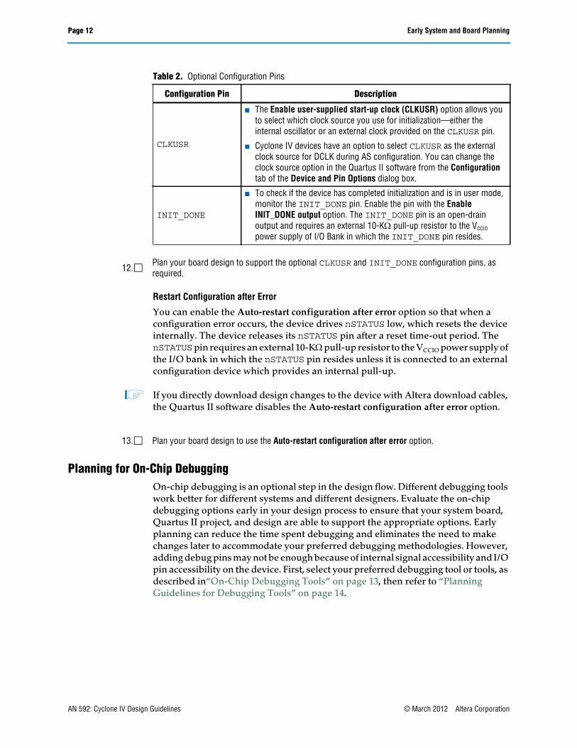
Optional Configuration Pins
Table 2 lists the optional configuration pins you can enable in the Cyclone IV device.
You can enable the Auto-restart configuration after error option so that when aconfiguration error occurs, the device drives nSTATUS low, which resets the deviceinternally. The device releases its nSTATUS pin after a reset time-out period. ThenSTATUSpin requires an external 10-Kpull-up resistor to the VCCIO power supply ofthe I/O bank in which the nSTATUS pin resides unless it is connected to an externalconfiguration device which provides an internal pull-up.
1 If you directly download design changes to the device with Altera download cables,the Quartus II software disables the Auto-restart configuration after error option.
Planning for On-Chip DebuggingOn-chip debugging is an optional step in the design flow. Different debugging toolswork better for different systems and different designers. Evaluate the on-chipdebugging options early in your design process to ensure that your system board,Quartus II project, and design are able to support the appropriate options. Earlyplanning can reduce the time spent debugging and eliminates the need to makechanges later to accommodate your preferred debugging methodologies. However,adding debug pins may not be enough because of internal signal accessibility and I/Opin accessibility on the device. First, select your preferred debugging tool or tools, asdescribed in“On-Chip Debugging Tools” on page 13, then refer to “PlanningGuidelines for Debugging Tools” on page 14.
Table 2. Optional Configuration Pins
Configuration Pin Description
CLKUSR
■ The Enable user-supplied start-up clock (CLKUSR) option allows youto select which clock source you use for initialization—either theinternal oscillator or an external clock provided on the CLKUSR pin.
■ Cyclone IV devices have an option to select CLKUSR as the externalclock source for DCLK during AS configuration. You can change theclock source option in the Quartus II software from the Configurationtab of the Device and Pin Options dialog box.
INIT_DONE
■ To check if the device has completed initialization and is in user mode,monitor the INIT_DONE pin. Enable the pin with the EnableINIT_DONE output option. The INIT_DONE pin is an open-drainoutput and requires an external 10-K pull-up resistor to the VCCIO
power supply of I/O Bank in which the INIT_DONE pin resides.
12.Plan your board design to support the optional CLKUSR and INIT_DONE configuration pins, asrequired.
13. Plan your board design to use the Auto-restart configuration after error option.
On-Chip Debugging ToolsThe Quartus II portfolio of verification tools includes the following in-systemdebugging features:
■ SignalProbe incremental routing—Quickly routes internal signals to the I/O pinswithout affecting the routing of the original design. Starting with a fully routeddesign, select and route the signals for debugging to either previously reserved orcurrently unused I/O pins.
■ SignalTap II Embedded Logic Analyzer—Probes the state of internal and I/Osignals without using external equipment or extra I/O pins, while the design isrunning at full speed in an FPGA device. Defining custom trigger-condition logicprovides greater accuracy and improves the ability to isolate problems. It does notrequire external probes or changes to the design files to capture the state of theinternal nodes or I/O pins in the design; all captured signal data is stored in devicememory until you are ready to read and analyze the data. The SignalTap IIEmbedded Logic Analyzer works best for synchronous interfaces. For debuggingasynchronous interfaces, consider using SignalProbe or an external logic analyzerto accurately view the signals.
■ Logic Analyzer Interface—Allows you to connect and transmit internal FPGAsignals to an external logic analyzer for analysis, allowing you to take advantageof advanced features in your external logic analyzer or mixed signal oscilloscope.Use this feature to connect a large set of internal device signals to a small numberof output pins for debugging purposes and to multiplex signals with design I/Opins if required.
■ In-System Memory Content Editor—Provides read and write access to in-systemFPGAmemoriesandconstants throughtheJTAGinterfacesoyoucantestchangesto the memory content and constant values in the FPGA while the device isfunctioning in the system.
■ Virtual JTAG Megafunction—Allows you to build your own system-leveldebugging infrastructure, including processor-based debugging solutions anddebugging tools in the software for system-level debugging. Instantiate theSLD_VIRTUAL_JTAG megafunction directly in your HDL code to provide one ormore transparent communication channels to access parts of your FPGA designusing the JTAG interface of the device.
f For more information about these debugging tools, refer to the Virtual JTAG(SLD_VIRTUAL_JTAG) Megafunction User Guide and Section IV. In-System DesignDebugging in volume 3 of the Quartus II Handbook. The section overview providesmore information about choosing a debugging solution.
14.Take advantage of the on-chip debugging features to analyze internal signals and perform advanceddebugging techniques.
Page 14 Pin Connection Considerations for Board Design
Planning Guidelines for Debugging ToolsIf you intend to use the on-chip debugging tools, plan for the tool or tools whendeveloping the system board, Quartus II project, and design, as described in thefollowing checklist:
Pin Connection Considerations for Board DesignWhen designing the interfaces to the Cyclone IV device, various factors can affect thePCB design. This section contains important guidelines for the following topics:
■ “Device Power-Up”
■ “Power Pin Connections and Power Supplies” on page 16
■ “Configuration Pin Connections” on page 17
■ “Board-Related Quartus II Settings” on page 20
■ “Signal Integrity Considerations” on page 21
■ “Board-Level Simulation and Advanced I/O Timing Analysis” on page 22
The following section, “I/O and Clock Planning” on page 23, describes the I/O signalconnections for the FPGA, which also affect the board design.
f For more information about board design guidelines, refer to the Board DesignResource Center. This Resource Center points to application notes and otherdocumentation that can help you implement successful high-speed PCBs thatintegrate Altera devices with other elements.
15.Select the on-chip debugging scheme(s) early to plan memory and logic requirements, I/O pinconnections, and board connections.
16.If you want to use the SignalTap II Embedded Logic Analyzer, Logic Analyzer Interface, In-SystemMemory Content Editor, or Virtual JTAG Megafunction, plan your system and board with JTAGconnections that are available for debugging.
17.Plan for the small amount of additional logic resources used to implement the JTAG hub logic for theJTAG debugging features.
18.For debugging with the SignalTap II Embedded Logic Analyzer, reserve device memory resources tocapture data during system operation.
19.Reserve I/O pins for debugging with SignalProbe or the Logic Analyzer Interface so you do not have tochange the design or board to accommodate the debugging signals later.
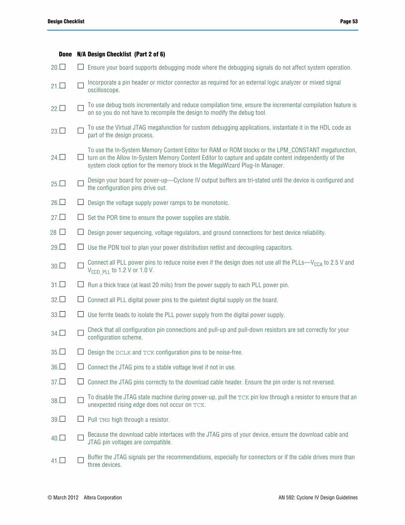
20.Ensure your board supports debugging mode where the debugging signals do not affect systemoperation.
21.Incorporate a pin header or mictor connector as required for an external logic analyzer or mixed signaloscilloscope.
22.To use debug tools incrementally and reduce compilation time, ensure the incremental compilationfeature is on so you do not have to recompile the design to modify the debug tool.
23.To use the Virtual JTAG megafunction for custom debugging applications, instantiate it in the HDLcode as part of the design process.
24.To use the In-System Memory Content Editor for RAM or ROM blocks or the LPM_CONSTANTmegafunction, turn on the Allow In-System Memory Content Editor to capture and update contentindependently of the system clock option for the memory block in the MegaWizard Plug-In Manager.
Pin Connection Considerations for Board Design Page 15
Device Power-UpCyclone IV device I/O pins are hot-socketing compliant without externalcomponents. You can insert or remove a Cyclone IV device from a powered-upsystem board without damaging or interfering with normal system and boardoperation.
You can drive signals into the I/O pins before or during power up or power downwithout damaging the device. Cyclone IV devices support power up or power downof the VCCINT, VCCA, and VCCIO pins in any sequence to simplify the system leveldesign. The individual power supply ramp-up and ramp-down rates can range from50 s to 50 ms. The power ramp must be monotonic.
In a hot socketing situation, the Cyclone IV device’s output buffers are turned offduring system power-up or power-down. Also, the Cyclone IV device does not driveout until the device is configured and working within the recommended operatingconditions.
Hot socketing circuitry is not available on configuration pins CONF_DONE, nCEO, andnSTATUS because they are required during configuration. Therefore, it is expectedbehavior for these pins to drive out during power-up and power-down sequences.
The POR circuit keeps the entire system in reset until the power supply voltage levelshave stabilized after power up. After power up, the device does not release nSTATUSuntil VCCINT, VCCA, and VCCIO for the I/O banks that contain configuration pins areabove the POR trip point of the device. After power down, brown-out occurs if theVCCINT or VCCA voltage sags below the POR trip point.
In Cyclone IV devices, you can select a fast or standard POR time, depending on theMSEL pin settings. The fast POR time is 3 ms < TPOR < 9 ms for a fast configurationtime. The standard POR time is 50 ms < TPOR < 200 ms, which has a lowerpower-ramp rate.
When power is applied to a Cyclone IV device, a POR event occurs if the powersupply reaches the recommended operating range within a certain period of time(specified as a maximum power supply ramp time; tRAMP). The maximum powersupply ramp time for Cyclone IV devices is 50 ms for standard POR or 3 ms for fastPOR, while the minimum power supply ramp time is 50 s.
Although power sequencing is not a requirement for correct operation, Alterarecommends considering the power-up timing of each rail to prevent problems withlong-term device reliability when designing a multi-rail powered system. You canreduce the device in-rush current with proper sequencing and voltage regulatordesign.
25.Design your board for power-up—Cyclone IV output buffers are tri-stated until the device isconfigured and the configuration pins drive out.
26. Design the voltage supply power ramps to be monotonic.
27. Set the POR time to ensure the power supplies are stable.
Page 16 Pin Connection Considerations for Board Design
1 Altera strongly recommends that you connect the GNDs between boards beforeconnecting power to ensure device reliability and compliance to the hot-socketingspecification.
f For more information, refer to the Power Requirements for Cyclone IV Devices chapter involume 1 of the Cyclone IV Device Handbook.
Power Pin Connections and Power SuppliesReview the power pin connection guidelines to determine the power supplies that arerequired in your system and which voltage inputs can share supplies. TheCyclone IV GX core voltage VCCINT is 1.2 V and the Cyclone IV E core voltage VCCINT is1.2 V or 1.0 V.
The I/O voltage VCCIO connections depend on the I/O standards of the design andsupport 1.2, 1.5, 1.8, 2.5, 3.0, and 3.3 V.
1 The device output pins do not meet the I/O standard specifications if the VCCIO level isout of the recommended operating range for the I/O standard.
f For more information about the supply voltages required for the Cyclone IV deviceand their recommended operation conditions, refer to the Power Requirements forCyclone IV Devices chapter in volume 1 of the Cyclone IV Device Handbook.
Voltage reference (VREF) pins serve as voltage references for certain I/O standards.The VREF pin is used mainly for voltage bias and does not source or sink muchcurrent. You can create the voltage with a regulator or resistor divider network. Formore information about VCCIO voltages andVREFpins for different I/O banks, refer to“Selectable I/O Standards and Flexible I/O Banks” on page 26.
f For more information about power supply types and power supply sharing orisolation, review the Cyclone IV Device Family Pin Connection Guidelines.
Decoupling CapacitorsBoard decoupling becomes more significant to improve overall power supply signalintegrity with increased power supply requirements.
Cyclone IV devices include embedded on-package and on-die decoupling capacitorsto provide high-frequency decoupling. These low-inductance capacitors suppresspower noise for excellent signal integrity performance and reduce the number ofexternal PCB decoupling capacitors, saving board space, reducing cost, and greatlysimplifying the PCB design.
Altera has created an easy-to-use power distribution network (PDN) design tool thatoptimizes the board-level PDN graphically. The purpose of the board-level PDN is todistribute power and return currents from the voltage regulating module (VRM) tothe FPGA power supplies, and to support optimal transceiver signal integrity andFPGA performance.
28 Design power sequencing, voltage regulators, and ground connections for best device reliability.
Pin Connection Considerations for Board Design Page 17
For each power supply, you must choose a network of bulk and ceramic decouplingcapacitors. While you can use the SPICE simulation to simulate the circuit, the PDNdesign tool provides a fast, accurate, and interactive way to determine the rightnumber of decoupling capacitors for optimal cost and performance trade-offs.
f For more information about the PDN design and optimization process, refer to thePower Delivery Network (PDN) Tool User Guide. You can also download the PowerDelivery Network (PDN) Tool.
PLL Board Design GuidelinesFor more information about designing your clock and PLL scheme, refer to “Clockand PLL Selection” on page 31 and “PLL Feature Guidelines” on page 33. Thefollowing checklist provides several considerations to design a power system forusing PLLs and minimizing jitter because PLLs contain analog componentsembedded in a digital device.
f For more information about the board design guidelines for the PLL power supplies,refer to the General Board Design Considerations/Guidelines section of the BoardDesign Resource Center.
Configuration Pin ConnectionsDependingonyourconfigurationscheme,differentpull-upandpull-downresistororsignal integrity requirements may apply. Some configuration pins also have specificrequirements if unused. You must correctly connect the configuration pins. Thissection describes guidelines to address common configuration pin connection issues.
f For a list of the dedicated and dual-purpose configuration pins, and a description ofthe function and connection guidelines, refer to the Configuration and Remote SystemUpgrades in Cyclone IV Devices chapter in volume 1 of the Cyclone IV Device Handbook.
DCLK and TCK Signal IntegrityThe TCK or DCLK traces, or both, must produce clean signals with no overshoot,undershoot, or ringing.
29. Use the PDN tool to plan your power distribution netlist and decoupling capacitors.
30.Connect all PLL power pins to reduce noise even if the design does not use all the PLLs—VCCA to 2.5 Vand VCCD_PLL to 1.2 V or 1.0 V.
31. Run a thick trace (at least 20 mils) from the power supply to each PLL power pin.
32. Connect all PLL digital power pins to the quietest digital supply on the board.
33. Use ferrite beads to isolate the PLL power supply from the digital power supply.
34.Check that all configuration pin connections and pull-up and pull-down resistors are set correctly foryour configuration scheme.
35. Design the DCLK and TCK configuration pins to be noise-free.
Page 18 Pin Connection Considerations for Board Design
When designing the board, lay out theTCKandDCLK traces with the same techniquesused to lay out a clock line. Any overshoot, undershoot, ringing, or other noise on theTCK signal can affect JTAG configuration. A noisy DCLK signal can affect AP, AS, PS,or FPP configuration and cause a CRC error. For a chain of devices, noise on any of theTCKorDCLKpins in the chain could cause the JTAG programming or configuration tofail for the entire chain.
f For more information about connecting devices in a chain, refer to the Configurationand Remote System Upgrades in Cyclone IV Devices chapter in volume 1 of the Cyclone IVDevice Handbook.
JTAG PinsBecause the JTAG configuration takes precedence over all other configurationmethods, the JTAG pins must not be left floating or toggling during configuration ifyou are not using the JTAG interface.
If you are using the JTAG interface, follow the guidelines in this section.
JTAG Pin Connections
A Cyclone IV device operating in JTAG mode uses four required pins (TDI,TDO,TMS,and TCK). The TCK pin has an internal weak pull-down resistor and the TDI and TMSpins have internal weak pull-up resistors (typically 25 K). All the JTAG pins arepowered by the VCCIO power supply of the I/O bank in which these pins reside.
If you have more than one device in the chain, connect the TDO pin of a device to theTDI pin of the next device in the chain.
Noise on the JTAG pins during configuration, user mode, or power-up can cause thedevice to go into an undefined state or mode.
Download Cable Operating Voltage
The operating voltage supplied to the Altera download cable by the target boardthrough the 10-pin header determines the operating voltage level of the downloadcable.
In a JTAG chain containing devices with different voltages, devices with a highervoltage must drive devices with the same or lower voltage. With this devicearrangement, a level shifter is required at the end of the chain. If this arrangement isnot possible, you must add more level shifters to the chain.
36. Connect the JTAG pins to a stable voltage level if not in use.
37. Connect the JTAG pins correctly to the download cable header. Ensure the pin order is not reversed.
38.To disable the JTAG state machine during power-up, pull the TCK pin low through a resistor to ensurethat an unexpected rising edge does not occur on TCK.
39. Pull TMS high through a resistor.
40.Because the download cable interfaces with the JTAG pins of your device, ensure the download cableand JTAG pin voltages are compatible.
Pin Connection Considerations for Board Design Page 19
f For more information about connecting a JTAG chain with multiple voltages acrossthe devices in the chain, refer to the JTAG Boundary Scan Testing for Cyclone IV Deviceschapter in volume 1 of the Cyclone IV Device Handbook.
JTAG Signal Buffering
You may have to add buffers to a JTAG chain, depending on the JTAG signal integrity,especially theTCK signal, because it is the JTAG clock and the fastest switching JTAGsignal. Because cables and board connectors tend to make bad transmission lines andintroduce noise to the signals, Altera recommends buffering the signals at theconnector.After this initialbufferat theconnector,addbuffersasthechaingets longeror whenever the signals cross a board connector.
If a cable drives three or more devices, buffer the JTAG signal at the cable connector toprevent signal deterioration. However, prevention of signal deterioration alsodepends on the board layout, loads, connectors, jumpers, and switches on the board.Anything added to the board that affects the inductance or capacitance of the JTAGsignals increases the likelihood that a buffer is added to the chain.
Each buffer must drive no more than eight loads for the TCK and TMS signals, whichdrive in parallel. If jumpers or switches are added to the path, decrease the number ofloads.
MSEL Configuration Mode PinsSelect the configuration scheme by driving the Cyclone IV device MSEL pins high orlow. The JTAG configuration is always available, regardless of MSEL pin selection.MSEL pins are powered by the VCCINT power supply. MSEL pins have 9-K internalpull-down resistors that are always active. To avoid problems detecting an incorrectconfiguration scheme, hardwire the MSEL pins to VCCA or GND without pull-up orpull-down resistors. You must not drive the MSEL pins with a microprocessor oranother device.
Other Configuration PinsEnsure all dedicated and dual-purpose configuration pins are connected correctly,including the nCE pin.
In a single-device configuration or JTAG programming, tienCE low. In a multi-deviceconfiguration, tie nCE low on the first device and connect its nCEO pin to the nCE pinon the next device in the chain.
41.Buffer the JTAG signals per the recommendations, especially for connectors or if the cable drivesmore than three devices.
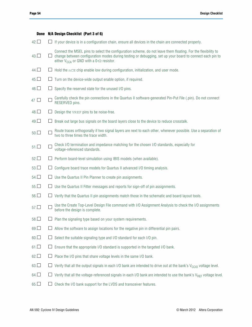
42. If your device is in a configuration chain, ensure all devices in the chain are connected properly.
43.Connect the MSEL pins to select the configuration scheme, do not leave them floating. For theflexibility to change between configuration modes during testing or debugging, set up your board toconnect each pin to either VCCA or GND with a 0- resistor.
44. Hold the nCE chip enable low during configuration, initialization, and user mode.
Page 20 Pin Connection Considerations for Board Design
Board-Related Quartus II SettingsThe Quartus II software provides options for the FPGA I/O pins that you mustconsider during board design. Ensure that these options are set correctly when youcreate the Quartus II project, and plan for their functionality during your boarddesign.
Device-Wide Output Enable PinCyclone IV devices support an optional chip-wide output enable pin that allows youto override all tri-states on the device I/Os. When this DEV_OE pin is driven low, allI/O pins are tri-stated; when this pin is driven high, all I/O pins behave asprogrammed. To use this chip-wide output enable, turn on Enable device-wideoutput enable (DEV_OE) on the General tab in the Device & Pin Options dialog boxin the Quartus II software before compiling your design.
Unused PinsTo allow flexibility in your board design, specify the state of the unused pins as one ofthe following five states in the Quartus II software:
■ As inputs that are tri-stated
■ As outputs that drive ground
■ As outputs that drive an unspecified signal
■ As input tri-stated with bus-hold
■ As input tri-stated with weak pull-up
c You must not connect the unused pins with outputs that drive ground to VCC oranother signal source because this can create problems that can damage the deviceoutput driver.
To improve signal integrity, set the unused pins as outputs that drive ground and tiethem directly to the ground plane on the board. Doing so reduces inductance bycreating a shorter return path and reduces noise on the neighboring I/O. To reducepower dissipation, set the clock pins to drive ground and set the other unused I/Opins as inputs that are tri-stated. If you set a reserved state for the unused pins, youmust not connect those pins to other devices on the board. To make the appropriatesettings, choose one of the five allowable states for the Reserve all unused pinsoption on the Unused Pins tab in the Device & Pin Options dialog box, or apply theReserve Pin assignment to specific pins in the Pin Planner.
45. Turn on the device-wide output enable option, if required.
46. Specify the reserved state for the unused I/O pins.
47Carefully check the pin connections in the Quartus II software-generated Pin-Put File (.pin). Do notconnect RESERVED pins.
Pin Connection Considerations for Board Design Page 21
When you compile your design, the Quartus II software generates the .pin to specifyhow you must connect the device pins. Unused I/O pins are marked in the report fileaccording to the unused pins option you set in the Quartus II software. All I/O pinsspecified as GND can either be connected to ground to improve the device’simmunity to noise, or left unconnected. Leave all RESERVED I/O pins unconnectedon your board because these I/O pins drive out unspecified signals. Tying aRESERVED I/O pin to VCC, ground, or another signal source can create problems thatcan damage the device output driver. You can connect the RESERVED_INPUT I/Opins to a high or low signal on the board and you can leave theRESERVED_INPUT_WITH_WEAK_PULLUP and RESERVED_INPUT_WITH_BUS_HOLDpins unconnected.
Signal Integrity ConsiderationsThis section describes a few board design guidelines related to the voltage referencepins, simultaneous switching noise, and I/O termination.
Voltage Reference PinsVoltage deviation on a VREF pin can affect the threshold sensitivity for inputs.
For more information about voltage reference pins and I/O standards, refer to “I/OFeatures and Pin Connections” on page 25.
Simultaneous Switching Noise (SSN)SSN becomes a concern when too many pins (in close proximity) change voltagelevels at the same time. Noise generated by SSN can reduce noise margin and causeincorrect switching.
f Although SSN is dominant on the device package, refer to the PCB guidelines in theBoard Design Resource Center for board layout recommendations that can helpreduce some of the noise.
For example, consider the following items:
I/O TerminationVoltage-referenced I/O standards require both an input reference voltage, VREF, and atermination voltage (VTT). The reference voltage of the receiving device tracks thetermination voltage of the transmitting device. Each voltage-referenced I/O standardrequires a unique termination setup. For example, a proper resistive signaltermination scheme is critical in SSTL2 standards to produce a reliable double datarate (DDR) memory system with superior noise margin.
Although single-ended, non-voltage-referenced I/O standards do not requiretermination, impedance matching is necessary to reduce reflections and improvesignal integrity.
48. Design the VREF pins to be noise-free.
49. Break out large bus signals on the board layers close to the device to reduce crosstalk.
50.Route traces orthogonally if two signal layers are next to each other, whenever possible. Use aseparation of two to three times the trace width.
Page 22 Pin Connection Considerations for Board Design
Cyclone IV on-chip series termination (RS OCT) provides the convenience of noexternal components. Alternatively, you can use external pull-up resistors toterminate voltage-referenced I/O standards such as SSTL and HSTL.
Differential I/O standards typically require a termination resistor between the twosignals at the receiver. The termination resistor must match the differential loadimpedance of the signal line.
For more information about the on-chip termination (OCT) features and limitations,refer to “I/O Features and Pin Connections” on page 25.
Board-Level Simulation and Advanced I/O Timing AnalysisTo ensure that I/O signaling meets the receiver threshold levels on your board setup,perform full board routing simulation with third-party board-level simulation toolsusing an IBIS model.
When this feature is available in the Quartus II software, select IBIS underBoard-level signal integrity analysis on the EDA Tool Settings page of the Settingsdialog box.
f For more information about this simulation flow, refer to the Signal Integrity withThird-Party Tools chapter in volume 3 of the Quartus II Handbook.
When you include an FPGA device with high-speed interfaces in a board design,knowing the signal integrity and board routing propagation delay is vital for propersystem operation. Altera recommends analyzing board level timing as part of I/O andboard planning, especially for high-speed designs.
You can configure board trace models of selected I/O standards and generate“board-aware” signal integrity reports with the Quartus II software. When you turnon the Enable Advanced I/O Timing option, the TimeQuest Timing Analyzer uses thesimulation results for the I/O buffer, package, and board trace model to generatemore accurate I/O delays and extra reports to give insight into signal behavior at thesystem level. You can use these advanced timing reports as a guide to make changesto the I/O assignments and board design to improve timing and signal integrity.
f For more information about board trace models for I/O analysis, refer to the I/OManagement chapter in volume 2 of the Quartus II Handbook.
51.Check I/O termination and impedance matching for the chosen I/O standards, especially forvoltage-referenced standards.
52. Perform board-level simulation using IBIS models (when available).
53. Configure board trace models for Quartus II advanced I/O timing analysis.
I/O and Clock PlanningPlanning and allocating I/O and clock resources is an important task with the highpin counts and advanced clock management and transceiver features in Cyclone IVdevices. Various considerations are important to effectively plan the available I/Oresources to maximize utilization and prevent issues related to signal integrity. Goodclock management systems are also crucial to the performance of an FPGA design.
The I/O and clock connections of your FPGA affect the rest of your system and boarddesign, so plan these connections early in your design cycle.
This section describes the following topics:
■ “Making FPGA Pin Assignments”
■ “Early Pin Planning and I/O Assignment Analysis” on page 24
■ “I/O Features and Pin Connections” on page 25
■ “Clock and PLL Selection” on page 31
■ “PLL Feature Guidelines” on page 33
■ “Clock Control Block” on page 34
■ “Simultaneous Switching Noise” on page 35
Making FPGA Pin AssignmentsWith the Quartus II Pin Planner GUI, you can identify I/O banks, VREF groups, anddifferential pin pairings to help you through the I/O planning process. Right-click inthe Pin Planner spreadsheet interface and click Pin Finder to search for specific pins.If you select migration devices, as described in “Vertical Device Migration” on page 5,the Pin Migration view highlights pins that change function in the migration devicewhen compared with the currently selected device.
You have the option of importing a Microsoft Excel spreadsheet into the Quartus IIsoftware to start the I/O planning process if you normally use a spreadsheet in yourdesignflow.YoucanalsoexportaComma-SeparatedValueFile (.csv) containingyourI/O assignments for spreadsheet use when all the pins are assigned.
When you compile your design in the Quartus II software, the I/O AssignmentAnalysis in the Fitter validates that the assignments meet all the device requirementsand generates messages if there are any problems.
54. Use the Quartus II Pin Planner to create pin assignments.
55. Use the Quartus II Fitter messages and reports for sign-off of pin assignments.
Quartus II designers can then pass the pin location information to PCB designers. Pinassignments must match between the Quartus II software and your schematic andboard layout tools to ensure the design works correctly on the board where it isplaced, especially if you must make changes to the pin-out. The Pin Planner is tightlyintegrated with certain PCB design EDA tools and can read pin location changes fromthese tools to check the suggested changes. When you compile your design, theQuartus II software generates the .pin. You can use this file to verify that each pin iscorrectly connected in board schematics.
f For more information about using the Pin Planner to create I/O assignments, refer tothe I/O Management chapter in volume 2 of the Quartus II Handbook. For moreinformation about passing I/O information between the Quartus II software andthird-party EDA tools, refer to the Mentor Graphics PCB Design Tools Support andCadence PCB Design Tools Support chapters in volume 2 of the Quartus II Handbook.
Early Pin Planning and I/O Assignment AnalysisIn many design environments, FPGA designers want to plan top-level FPGA I/O pinsearly so that board designers can start developing the PCB design and layout. TheFPGA device’s I/O capabilities and board layout guidelines influence pin locationsand other types of assignments. In cases where the board design team specifies anFPGA pin-out, it is crucial that you verify pin locations in the FPGA placement androuting software as soon as possible to avoid board design changes.
The Quartus II Pin Planner enables easy I/O pin assignment planning, assignment,and validation, as described in “Making FPGA Pin Assignments” on page 23. TheQuartus II Start I/O Assignment Analysis command checks that the pin locations andassignments are supported in the target FPGA architecture. Checks include referencevoltage pin usage, pin location assignments, and mixing of I/O standards. You canuse I/O Assignment Analysis to validate I/O-related assignments that you create ormodify throughout the design process.
Starting FPGA pin planning early improves the confidence in early board layouts,reduces the chance of error, and improves the design’s overall time to market. You cancreate a preliminary pin-out for an Altera FPGA using the Quartus II Pin Plannerbefore the source code is designed.
Early in the design process, the system architect typically has information about thestandard I/O interfaces (such as memory and bus interfaces), IP cores to be used inthe design, and any other I/O-related assignments defined by the systemrequirements. The Pin Planner Create/Import Megafunction feature interfaces withthe MegaWizard™ Plug-In Manager and allows you to create or import custommegafunctions and IP cores that use I/O interfaces. Enter PLL, LVDS, and transceiverblocks that can affect the pin placement rules. When you have entered as much
56. Verify that the Quartus II pin assignments match those in the schematic and board layout tools.
57.Use the Create Top-Level Design File command with I/O Assignment Analysis to check the I/Oassignments before the design is complete.
I/O-related information as possible, generate a top-level design netlist file using theCreate Top-Level Design File command. You can use the I/O analysis results tochange pin assignments or IP parameters and repeat the checking process until theI/O interface meets your design requirements and passes the pin checks in theQuartus II software.
When planning is complete, you can pass the preliminary pin location information tothe PCB designers as described in the previous section. When the design is complete,use the reports and messages generated by the Quartus II Fitter for the final sign-off ofpin assignments.
f For more information about I/O assignment and analysis, refer to the I/O Managementchapter in volume 2 of the Quartus II Handbook.
I/O Features and Pin ConnectionsCyclone IV I/Os are designed for ease of use and rapid system integration, whilesimultaneously providing high bandwidth and support for common interfaces.Independent modular I/O banks with a common bank structure for verticalmigration lend efficiency and flexibility to the high-speed I/O. This section providesguidelines related to I/O features and pin connections. It describes support fordifferent I/O signal types and I/O standards in device I/O banks, as well as otherI/O features available for your design. It also provides information about memoryinterfaces, pad placement guidelines, and special pin connections.
f For more information about pin connections, refer to the Cyclone IV Device Family PinConnection Guidelines.
I/O Signaling TypeCyclone IV devices support a wide range of industry I/O standards, includingsingle-ended, voltage-referenced single-ended, and differential I/O standards. Thissection provides general guidelines for selecting a signaling type.
Single-ended I/O signaling provides a simple rail-to-rail interface. Its speed is limitedby the large voltage swing and noise. Single-ended I/Os do not require termination,unless reflection in the system causes undesirable effects.
Voltage-referenced signaling reduces the effects of simultaneous switching outputs(SSO) from pins changing voltage levels at the same time (for example, externalmemoryinterfacedataandaddressbuses).Voltage-referencedsignalingalsoprovidesan improved logic transition rate with a reduced voltage swing and minimizes noisecausedbyreflectionwithaterminationrequirement.However,additionalterminationcomponents are required for the reference voltage source, VTT.
Differential signaling eliminates the interface performance barrier of single-endedand voltage-referenced signaling, with superior speed using an additional invertedclosely-coupled data pair. Differential signaling also avoids the requirement for aclean reference voltage. This is possible because of lower swing voltage and noiseimmunity with common mode noise rejection capability. Considerations for thisimplementation include the requirements for a dedicated PLL to generate a samplingclockandmatchedtracelengthstoeliminatethephasedifferencebetweenaninvertedand non-inverted pair.
Cyclone IV I/O pins are organized in pairs to support differential standards. EachI/O pin pair can support differential input or output operations, with the exception ofcertain clock pins that support differential input operations only. In your designsource code, define just one pin to represent a differential pair and create a pinassignment for this positive end of the pair. When you specify a differential I/Ostandard, the Quartus II software automatically places the corresponding negativepin.
Selectable I/O Standards and Flexible I/O BanksCyclone IV I/O pins are grouped together into I/O banks and each bank has aseparate power bus. Each device I/O pin is associated with one I/O bank. Cyclone IVE devices have eight I/O banks. Cyclone IV GX devices have up to 10 I/O banks andone configuration bank. The Cyclone IV GX configuration I/O bank contains threeuser I/O pins with secondary configuration programming functions. They can beused as normal user I/O pins if they are not used in configuration modes.
All single-ended I/O standards are supported except HSTL-12 Class II, which is onlysupported in column I/O banks. All differential I/O standards are supported in top,bottom, and right I/O banks. The only exception is HSTL-12 Class II, which is onlysupported in column I/O banks. The entire left side of the Cyclone IV GX devicescontainsdedicatedhigh-speedtransceiverbanksforhigh-speedtransceiversinterfaceapplications.
You can assign I/O standards and make other I/O-related settings in the Pin Planner.Be sure to use the correct dedicated pin inputs for signals such as clocks and globalcontrol signals, as described in “Clock and PLL Selection” on page 31.
The board must supply each bank with one VCCIO voltage level for everyVCCIOpin inthe bank. Each I/O bank is powered by the VCCIO pins of that particular bank and isindependent of the VCCIO power supply of other I/O banks. A single I/O banksupports output signals that are driving at the same voltage as the VCCIO powersupply. An I/O bank can simultaneously support any number of input signals withdifferent I/O standards, with some exceptions for voltage-referenced inputs.
58. Plan the signaling type based on your system requirements.
69. Allow the software to assign locations for the negative pin in differential pin pairs.
60. Select the suitable signaling type and I/O standard for each I/O pin.
61. Ensure that the appropriate I/O standard is supported in the targeted I/O bank.
62. Place the I/O pins that share voltage levels in the same I/O bank.
63.Verify that all the output signals in each I/O bank are intended to drive out at the bank’s VCCIO voltagelevel.
64.Verify that all the voltage-referenced signals in each I/O bank are intended to use the bank’s VREFvoltage level.
Voltage-referenced standards are supported in an I/O bank using any number ofsingle-ended or differential standards, as long as they use the same VREF and VCCIO
values. For example, if you choose to implement both SSTL-2 and SSTL-18 in yourCycloneIVdevices, theI/Opinsusingthesestandards(becausetheyrequiredifferentVREF values) must be in different banks from each other. However, the same I/O bankcan support SSTL-2 and 2.5-V LVCMOS with the VCCIO set to 2.5 V and the VREF set to1.25 V.
1 When you use the VREF pins as regular I/Os, they have higher pin capacitance thanregular user I/O pins. This has an impact on the timing if the pins are used as inputsand outputs.
f For more information about VREF pin capacitance, refer to the “Pin Capacitance”section in the Cyclone IV Device Data Sheet chapter in volume 3 of the Cyclone IV DeviceHandbook. For more information about how to identify VREF groups, refer to theCyclone IV Device Family Pin-Out Files or the Quartus II Pin Planner tool.
Different I/O banks include different support for LVDS signaling and the Cyclone IVtransceiver banks include additional support.
f For information about the number of channels available for the LVDS I/O standard,refer to the I/O Feature in Cyclone IV Devices chapter in volume 1 of the Cyclone IVDevice Handbook. For more information about transceiver bank-related features, referto the Cyclone IV Transceivers Architecture chapter in volume 2 of the Cyclone IV DeviceHandbook.
f For more information about I/Os, refer to the I/O Features in Cyclone IV Deviceschapter in volume 2 of the Cyclone IV Device Handbook. Refer to the Cyclone IV I/Obanks figures that show the location of each I/O bank and what each bank supports.The figures describing the number of I/Os in each bank provides bank informationspecific to each device density. When designing LVTTL and LVCMOS inputs withCyclone IV devices, refer to the section describing the I/O banks guidelines.
f For more information about the electrical characteristics of each I/O standard, refer tothe Cyclone IV Device Data Sheet chapter in volume 3 of the Cyclone IV Device Handbook.
Placement Guidelines Related to Differential I/O PinsThe placement of single-ended I/O pins with respect to differential LVDS I/O pins isrestricted. Follow the pin placement rules that specify the number of I/O pins thatmust separate single-ended outputs and LVDS I/O. During compilation, theQuartus II Fitter verifies that these guidelines are satisfied. After compilation, theQuartus II software generates a fitter report that summarizes the guidelines checkedby the Quartus II software during compilation.
65. Check the I/O bank support for the LVDS and transceiver features.
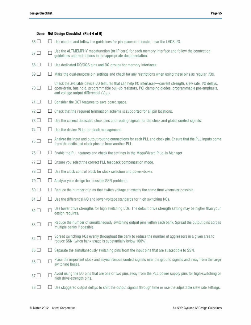
66. Use caution and follow the guidelines for pin placement located near the LVDS I/O.
The VCCIO power supply for a bank is susceptible to noise from switching outputs inthe bank. To maintain an acceptable noise level on the VCCIO power supply, there arerestrictions on the placement of single-ended I/O pads in relation to differential pads.The Quartus II software automatically checks for these restrictions.
When there are single-ended voltage-referenced inputs in a bank, the Quartus IIsoftware automatically checks for restrictions on the placement of outputs in relationto VREF pads and supply pairs (VCCIO and GND). The restriction is in place tomaintain an acceptable noise level on the VCCIO power supply and to prevent outputswitching noise from shifting the VREF rail.
Memory InterfacesCyclone IV devices provide an efficient architecture to quickly and easily fit wideexternal memory interfaces with their small modular I/O bank structure banks.Cyclone IV devices support existing and emerging external DDR memory standards,such as DDR2 SDRAM, DDR SDRAM, and QDR II SRAM. Cyclone IV devicessupport DDR external memory on the top, bottom, and right I/O banks.
Aself-calibratingmegafunction(ALTMEMPHY)isoptimizedtotakeadvantageoftheCyclone IV I/O structure and the Quartus II TimeQuest Timing Analyzer. Themegafunction allows you to set the external memory interface features and helps setup the physical interface (PHY) best suited for your system with the highest reliablefrequency of operation. When using the Altera memory controller MegaCore®
functions, the ALTMEMPHY megafunction is instantiated for you.
If you design multiple memory interfaces into the device using Altera IP, generate aunique interface for each instance to ensure good results instead of designing it onceand instantiating it multiple times.
The data strobe DQS and data DQ pin locations are fixed in the Cyclone IV device.Before you design your device pin-out, refer to the memory interface guidelines fordetails and important restrictions related to the connections for these and othermemory-related signals.
f For more information about connecting a Cyclone IV device with external memorydevices, includingthemaximumsupportedclockratefordifferentmemorystandardsand restrictions on pin placement, refer to the External Memory Interfaces in Cyclone IVDevices chapter in volume 1 of the Cyclone IV Device Handbook. For additionalresources, refer to the External Memory Solutions Center.
f For more information about the Cyclone IV PLL, refer to the Clock Networks and PLLsin Cyclone IV Devices chapter in the Cyclone IV Device Handbook. For more informationabout the ALTMEMPHY megafunction, refer to the External DDR Memory PHYInterface (ALTMEMPHY) Megafunction User Guide.
67.Use the ALTMEMPHY megafunction (or IP core) for each memory interface and follow the connectionguidelines and restrictions in the appropriate documentation.
68. Use dedicated DQ/DQS pins and DQ groups for memory interfaces.
Dual-Purpose and Special Pin ConnectionsCyclone IV devices allow I/O flexibility with dual-purpose configuration pins. Youcan use dual-purpose configuration pins as general I/Os after device configuration iscomplete. Select the necessary setting for each of the dual-purpose pins on theDual-Purpose Pins tab of the Device and Pin Options dialog box. Depending on theconfiguration scheme, these pins can be reserved as regular I/O pins, as inputs thatare tri-stated, as outputs that drive ground, or as outputs that drive an unspecifiedsignal.
You can also use dedicated clock inputs, which drive to the GCLK networks, asgeneral-purpose input pins if not used as clock pins. When you use the clock inputs asgeneral inputs, the I/O registers use LE-based registers because the clock input pinsdo not include dedicated I/O registers.
If not enabled, the device-wide reset and clear pins are available as design I/Os. Formore information, refer to “Device-Wide Output Enable Pin” on page 20 and“Register Power-Up Levels and Control Signals” on page 37.
Cyclone IV I/O FeaturesThe Cyclone IV device IOE offers a range of programmable features for an I/O pin.These features increase the flexibility of I/O utilization and provide an alternative toreducetheusageofexternaldiscretecomponents toon-chip,suchasapull-upresistorand diode. Table 3 lists Cyclone IV I/O features, provides usage information anddesign considerations, and provides references for more information about thefeatures.
69.Make the dual-purpose pin settings and check for any restrictions when using these pins as regularI/Os.
Table 3. Cyclone IV I/O Features (Part 1 of 3)
Feature Usage Guidelines and More Information
MultiVolt I/O Interface
Allows all packages to interface with systems ofdifferent supply voltages. VCCIO pins can beconnected to a 1.5-, 1.8-, 2.5-, 3.0, or 3.3-Vpower supply, depending on the outputrequirements. The output levels are compatiblewith systems of the same voltage as the powersupply.
For a summary of MultiVolt I/O support, a list ofthe supported I/O standards and the typicalvalues for input and output VCCIO, VREF, and boardtermination voltage (VTT), refer to the I/OFeatures in Cyclone IV Devices chapter involume 1 of the Cyclone IV Device Handbook.
3.3-V I/O Interface
Cyclone IV I/O buffers support 3.3-V I/Ostandards as transmitters or receivers in yoursystem. The output high voltage (VOH), outputlow voltage (VOL), input high voltage (VIH), andinput low voltage (VIL) levels meet the 3.3-V I/Ostandards specifications when the Cyclone IVVCCIO voltage is powered by 3.3 V.
To ensure device reliability and proper operationwhen interfacing with a 3.3 V I/O system, youmust ensure that the absolute maximum ratingsof the Cyclone IV devices are not violated.
Altera recommends performing IBIS simulationto determine that the overshoot and undershootvoltages are within the guidelines. For moreinformation, refer to the I/O Features inCyclone IV Devices chapter in volume 1 of theCyclone IV Device Handbook.
Programmable current-strength controlavailable for certain I/O standards. This canmitigate the effects of high signal attenuationdue to a long transmission line or a legacybackplane. A higher current strength increasesI/O performance, but also increases noise onthe interface, so you can use current strengthcontrol to manage noise.
Ensure that the output buffer current strength issufficiently high, but does not cause excessiveovershoot or undershoot that violates voltagethreshold parameters for the I/O standard.
Altera recommends performing IBIS or SPICEsimulations to determine the right currentstrength setting for your specific application.For a list of standards and settings, refer to theI/O Features in Cyclone IV Devices chapter involume 1 of the Cyclone IV Device Handbook.
Programmable SlewRate Control
Configure each pin for low-noise or high-speedperformance. A faster slew rate provideshigh-speed transitions. You can use faster slewrates to improve the available timing margin inmemory-interface applications or when theoutput pin has a high-capacitive loading. A slowslew rate can help reduce system noise, butadds a nominal delay to the rising and fallingedges. You can use slew rate to reduce SSN.
Confirm that your interface meets itsperformance requirements if you use slowerslew rates.
Altera recommends performing IBIS or SPICEsimulations to determine the right slew ratesetting for your specific application.
Programmable IOEDelay
Programmable delay chains can ensure zerohold times, minimize setup times, or increaseclock-to-output times. You can use delays asdeskewing circuitry to ensure that all bits of abus have the same delay going into or out of thedevice.
The Quartus II compiler can program thesedelays to automatically minimize setup timewhile providing a zero hold time. Programmabledelays can increase the register-to-pin delaysfor output registers.
For more information about the delayspecifications, refer to the Cyclone IV DeviceData Sheet chapter in volume 3 of theCyclone IV Device Handbook.
For more information about how to set the inputand output pin delay, refer to the Area andTiming Optimization chapter in volume 2 of theQuartus II Handbook.
Programmable OutputBuffer Delay
Delay chains in the single-ended output buffercan independently control the rising and fallingedge delays of the output buffer.
You can use delays to adjust the output bufferduty cycle, compensate channel-to-channelskew, reduce SSO noise by deliberatelyintroducing channel-to-channel skew, andimprove high-speed memory-interface timingmargins.
Open-Drain Output
When configured as open-drain, the logic valueof the output is either high-Z or 0. Used insystem-level control signals that can beasserted by multiple devices in the system.
An external pull-up resistor is required toprovide logic high.
For more information, consider the following checklist items and refer to theappropriate documentation:
Clock and PLL SelectionThe first stage in planning your clocking scheme is to determine your system clockrequirements. Understand your device’s available clock resources andcorrespondingly plan the design clocking scheme. Consider your requirements fortiming performance and how much logic is driven by a particular clock.
Bus Hold
Weakly holds the signal on an I/O pin at its lastdriven state until the next input signal ispresent. With this feature, an external pull-up orpull-down resistor to hold a signal level whenthe bus is tri-stated is not required. The circuitryalso pulls non-driven pins away from the inputthreshold voltage where noise can causeunintended high-frequency switching.
If you enable the bus-hold feature, you cannotuse the programmable pull-up option. Disablethe bus-hold feature if the I/O pin is configuredfor differential signals.
For more information about sustaining currentdriven through this resistor and the overdrivecurrent used to identify the next driven inputlevel for each VCCIO voltage level, refer to theCyclone IV Device Data Sheet chapter in volume3 of the Cyclone IV Device Handbook.
Programmable Pull-UpResistor
A pull-up resistor weakly holds the I/O to theVCCIO level when in user mode. Can be used withopen-drain output to eliminate the requirementfor an external pull-up resistor.
If you enable the programmable pull-up option,you cannot use the bus-hold feature.
PCI Clamping Diode
Can be used to protect the pin from excessiveovershoot voltage in 3.3-V LVTTL,3.3-V LVCMOS, 3.0-V LVTTL, 3.0-V LVCMOS,2.5-V LVTTL/LVCMOS, PCI and PCI-X I/Ostandard interfaces.
If the input I/O standard is 3.3-V LVTTL,3.3-V LVCMOS, 3.0-V LVTTL, 3.0-V LVCMOS,2.5-V LVTTL/LVCMOS, PCI, or PCI-X, the PCIclamp diode is enabled by default in theQuartus II software.
OCT
Driver-impedance matching provides the I/Odriver with controlled output impedance thatclosely matches the impedance of thetransmission line to significantly reducereflections. OCT maintains signal quality, savesboard space, and reduces external componentcosts. Cyclone IV devices support the RS OCTwith or without calibration. Cyclone IV devicesprovide a series termination value of 25-and50-.
RS OCT is supported on any I/O bank. VCCIO andVREF must be compatible for all I/O pins toenable RS OCT in a given I/O bank. I/O standardsthat support different RS values can be locatedin the same I/O bank as long as their VCCIO andVREF are not conflicting.
For more information, refer to the I/O Featuresin Cyclone IV Devices chapter in volume 1 of theCyclone IV Device Handbook.
ProgrammablePre-Emphasis andVOD
Increases the amplitude of the high frequencycomponent of the output signal and helps tocompensate for the frequency dependentattenuation along the transmission line.
For more information, refer to the Cyclone IVDevice I/O Features chapter in volume 1 of theCyclone IV Device Handbook.
Table 3. Cyclone IV I/O Features (Part 3 of 3)
Feature Usage Guidelines and More Information
70.Check the available device I/O features that can help I/O interfaces—current strength, slew rate, I/Odelays, open-drain, bus hold, programmable pull-up resistors, PCI clamping diodes, programmablepre-emphasis, and voltage output differential (VOD).
71. Consider the OCT features to save board space.
72. Check that the required termination scheme is supported for all pin locations.
Cyclone IV GX devices provide up to 12 dedicated clock pins (CLK[15..4]) that candrive the GCLKs. Cyclone IV GX devices support four dedicated clock pins on eachside of the device except the left side of the device. These clock pins can drive up to 30GCLKs. Cyclone IV E devices provide up to 15 dedicated clock pins (CLK[15..1])that can drive up to 20 GCLKs. Cyclone IV E devices support three dedicated clockpins on the left side and four dedicated clock pins on the top, right, and bottom sidesof the device except EP4CE6 and EP4CE10 devices. EP4CE6 and EP4CE10 devicesonly support three dedicated clock pins on the left side and four dedicated clock pinson the right side of the device.
Cyclone IV GX devices offer two variations of PLLs—GPLLs and the MPLLs.Cyclone IV E devices only have GPLLs. The GPLLs are used for general-purposeapplications in the FPGA fabric and periphery such as external memory interfaces.The MPLLs are used for clocking the transceiver blocks. When the MPLLs are notused for transceiver clocking, they can be used for general-purpose clocking. Thereare up to eight GPLLs and MPLLs that provide robust clock management andsynthesis for device clock management, external system clock management, andhigh-speed I/O interfaces in Cyclone IV GX devices.
f For more information about the number of GCLK networks, GPLLs, and MPLLs ineach device density, refer to the Cyclone IV FPGA Device Family Overview chapter involume 1 of the Cyclone IV Device Handbook.
The dedicated clock pins drive the clock network directly, ensuring lower skew thanother I/O pins. Use the dedicated routing network to achieve predictable delay withless skew for the high fan-out signals. You can also use the clock pins and clocknetwork to drive the control signals such as asynchronous reset.
Specific clock inputs connect to specific PLLs that can drive specific low-skew routingnetworks. Analyze the global resource availability for each PLL and the PLLavailability for each clock input pin.
73. Use the correct dedicated clock pins and routing signals for the clock and global control signals.
Use the following descriptions to help determine which clock networks areappropriate for the clock signals in your design:
■ The GCLK networks can drive throughout the entire device, serving as low-skewclock sources for device logic. This clock region has the maximum delay whencompared with to other clock regions but allows the signal to reach everywherewithin the device. This option is good for routing global reset and clear signals orrouting clocks throughout the device.
■ IOEs and internal logic can also drive GCLKs to create internally generatedGCLKs and other high fan-out control signals; for example, synchronous orasynchronous clears and clock enables.
■ PLLs cannot be driven by internally generated GCLKs. The input clock to the PLLmust come from dedicated clock input pins, fed by a pin-driven dedicated GCLK,or through a clock control block if the clock control block is fed by an output fromanother PLL or a pin-driven dedicated GCLK.
f Formoreinformationaboutthesefeaturesanddetailedclockconnectioninformation,refer to the Clock Networks and PLLs in Cyclone IV Devices chapter in volume 1 of theCyclone IV Device Handbook.
If your system requires more clock or control signals than are available in the targetdevice, consider cases when you can spare the dedicated clock resource, particularlylow fan-out and low-frequency signals where clock delay and clock skew do not havea significant impact on design performance. Use the Global Signal assignment in theQuartus II Assignment Editor to select the type of global routing or set the assignmentto Off to specify that the signal must not use global routing resources.
PLL Feature GuidelinesBased on your system requirements, define the required clock frequencies for yourFPGA design, and the input frequencies that will be available to the FPGA. Use thesespecificationstodetermineyourPLLscheme.UsetheQuartusIIMegaWizardPlug-InManager to enter your settings for the ALTPLL megafunction and check the results toverify whether you can implement particular features and input and outputfrequencies in a particular PLL.
f For more information about setting up your timing constraints to work with the PLL,refer to AN 471: High-Performance FPGA PLL Analysis with TimeQuest.
Cyclone IV PLLs provide robust clock management and synthesis for device clockmanagement, external system clock management, and high-speed I/O interfaces. AllCyclone IV PLLs support several features for general-purpose clock management.Use the following features when planning your PLL design.
f For more information about the PLL features, refer to the Clock Networks and PLLs inCyclone IV Devices chapter in the Cyclone IV Device Handbook.
75.Analyze the input and output routing connections for each PLL and clock pin. Ensure that the PLLinputs come from the dedicated clock pins or from another PLL.
76. Enable the PLL features and check the settings in the MegaWizard Plug-In Manager.
f For more information about designing your PLL and using the ALTPLL megafunctionto take advantage of the features described in this section, refer to the Phase-LockedLoops (ALTPLL) Megafunction User Guide.
Clock Feedback ModeCyclone IV PLLs support the following five clock feedback modes:
■ Source synchronous mode
■ No compensation mode
■ Normal mode
■ Zero delay buffer (ZDB) mode
■ Deterministic latency compensation mode
Each mode compensates for different clock networks and delays so the clocks arealigned differently. Choose the correct feedback mode for your application.
Clock SwitchoverThe clock switchover feature allows the PLL to switch between two reference inputclocks. Use this feature for clock redundancy or for a dual clock domain application;for example, when a system turns on the redundant clock if the previous clock stopsrunning. The design can perform clock switchover automatically when the clock is nolonger toggling or based on a user control signal (clkswitch).
Clock Control BlockIn Cyclone IV devices, dedicated clock input pins, PLL counter outputs, dual-purposeclock I/O inputs, and internal logic can all feed the clock control block for each GCLK.The output from the clock control block in turn feeds the corresponding GCLK. TheGCLK can drive the PLL input if the clock control block inputs are outputs of anotherPLL or dedicated clock input pins. There are five or six clock control blocks on eachside of the device periphery, depending on device density, providing up to 30 clockcontrol blocks in each Cyclone IV GX device. There are a maximum of 20 clock controlblocks available in each Cyclone IV E device.
The control block has two functions:
■ Dynamic GCLK clock source selection (not applicable for the dual-purpose clock[DPCLK] and internal logic input)
■ GCLK network power down (dynamic enable and disable)
Use these features to select different clock input signals or power-down clocknetworks to reduce power consumption without using combinational logic in yourdesign. In Cyclone IV devices, the clock enable signals are supported at the clocknetwork level instead of at the PLL output counter level so you can turn off a clockeven when a PLL is not being used. You can select a clock source statically with asetting in the Quartus II software or dynamically using internal logic to drive themultiplexer select inputs.
77. Ensure you select the correct PLL feedback compensation mode.
78. Use the clock control block for clock selection and power-down.
f For more information about using the ALTCLKCTRL megafunction toset upthe clockcontrol block, refer to the Clock Control Block (ALTCLKCTRL) Megafunction User Guide.
Simultaneous Switching NoiseSSN becomes a concern when too many pins (in close proximity) change voltagelevels at the same time. Consider the following checklist recommendations whenplanning I/O and clock connections:
For more information about the features you can use, refer to “Cyclone IV I/OFeatures” on page 29.
Design EntryIn the development of complex FPGA designs, design practices and coding styleshave an enormous impact on your device’s timing performance, logic utilization, andsystem reliability. You can also use megafunctions and SOPC Builder to help designyour FPGA system. In addition, when planning and creating the design, plan for ahierarchical or team-based design to improve design productivity.
Design RecommendationsIn a synchronous design, a clock signal triggers all events. When all of the registers’timing requirements are met, a synchronous design behaves in a predictable andreliable manner for all process, voltage, and temperature (PVT) conditions. You caneasily target synchronous designs to different device families or speed grades.
Problems with asynchronous design techniques include reliance on propagationdelays in a device, incomplete timing analysis, and possible glitches.
79. Analyze your design for possible SSN problems.
80. Reduce the number of pins that switch voltage at exactly the same time whenever possible.
81. Use the differential I/O and lower-voltage standards for high switching I/Os.
82.Use lower drive strengths for high switching I/Os. The default drive strength setting may be higherthan your design requires.
83.Reduce the number of simultaneously switching output pins within each bank. Spread the output pinsacross multiple banks if possible.
84.Spread switching I/Os evenly throughout the bank to reduce the number of aggressors in a given areato reduce SSN (when bank usage is substantially below 100%).
85. Separate the simultaneously switching pins from the input pins that are susceptible to SSN.
86.Place the important clock and asynchronous control signals near the ground signals and away fromthe large switching buses.
87.Avoid using the I/O pins that are one or two pins away from the PLL power supply pins forhigh-switching or high drive-strength pins.
88.Use staggered output delays to shift the output signals through time or use the adjustable slew ratesettings.
89. Use synchronous design practices. Pay attention to the clock signals.
Pay particular attention to your clock signals because they have a strongly effect onyour design’s timing accuracy, performance, and reliability. Problems with clocksignals can cause functional and timing problems in your design. Use dedicated clockpins and clock routing for best results. For clock inversion, multiplication, anddivision, use the device PLLs. For clock multiplexing and gating, use the dedicatedclock control block or PLL clock switchover feature instead of combinational logic. Formore information, refer to “PLL Board Design Guidelines” on page 17. If you mustuse internally generated clock signals, register the output of any combinational logicused as a clock signal to reduce glitches. For example, if you divide a clock usingcombinational logic, clock the final stage with the clock signal that was used to clockthe divider circuit.
Design Assistant in the Quartus II software is a design-rule checking tool that allowsyou to check for design issues early in the design flow. The Design Assistant checksyour design for adherence to the Altera-recommended design guidelines or designrules. To run Design Assistant, on the Processing menu, point to Start and click StartDesign Assistant. To set Design Assistant to run automatically during compilation,turn on Run Design Assistant during compilation in the Settings dialog box. Youcan also use third-party “lint” tools to check your coding styles.
f For more information about design recommendations and using the Design Assistantfeature, refer to the Design Recommendations for Altera Devices and the Quartus II DesignAssistant chapter in volume 1 of the Quartus II Handbook. You can also refer to industrypapers for more information about multiple clock design. For a good analysis ofmulti-asynchronous clock designs, refer to Synthesis and Scripting Techniques forDesigning Multi-Asynchronous Clock Designs.
Using MegafunctionsAltera provides parameterizable megafunctions that are optimized for Altera devicearchitectures. Instead of coding your own logic, you can save design time usingmegafunctions.Additionally,Altera-providedmegafunctionscanoffermoreefficientlogic synthesis and device implementation.You can scale the megafunction’s size andset various options using parameters. Megafunctions include the library ofparameterized modules (LPM) and Altera device-specific megafunctions. You canalso take advantage of Altera and third-party IP and reference designs to save designtime, as described in “IP Selection” on page 2.
The Quartus II MegaWizard Plug-In Manager provides a user interface to customizemegafunctions. Altera recommends building or changing megafunction parametersusing the MegaWizard Plug-In Manager to ensure you set all the ports andparameters correctly.
f For more information about specific megafunctions, refer to Quartus II Help or themegafunction user guides on the Literature: User Guides page.
90. Use the Quartus II Design Assistant to check design reliability.
91. Use megafunctions with the MegaWizard Plug-In Manager.
Recommended HDL Coding StylesHDL coding styles can have a significant effect on the quality of results (QoR) forprogrammable logic designs. Use the Altera-recommended coding styles to achieveoptimal synthesis results. When designing memory and digital system processing(DSP) functions, it is helpful to understand the device architecture so you can takeadvantage of the dedicated logic block sizes and configurations.
f For more information about specific HDL coding examples and recommendations,refer to the Recommended HDL Coding Styles chapter in volume 1 of the Quartus IIHandbook. You can refer to your synthesis tool’s documentation for any additionaltool-specific guidelines. In the Quartus II software, you can use the HDL examples inthe Language Templates available from the right-click menu in the text editor.
Register Power-Up Levels and Control SignalsCyclone IV devices support an optional chip-wide reset that allows you to override allclears on all the device registers, including the memory block registers (but not thememory contents itself). When the DEV_CLRn pin is driven low, all registers arecleared or reset to 0.
The following sections describe situations when synthesis performs an optimizationcalled “NOT gate push back”, where affected registers behave as though they arepreset to a high value when DEV_CLRn is driven low. When the DEV_CLRn pin isdriven high, all registers behave as programmed. To use this chip-wide reset, beforecompiling your design, turn on Enable device-wide reset (DEV_CLRn) in theQuartus II software on the General tab of the Device & Pin Options dialog box.
Each Cyclone IV logic array block (LAB) contains dedicated logic for driving registercontrol signals to its LEs. The control signals include two clocks, two clock enables,twoasynchronousclears,onesynchronousclear,andoneasynchronousload.Registercontrol signals restrict how the registers are packed into the LABs because signals areshared within the LAB. It is important that the control signals use the dedicatedcontrol signals in the device architecture. In some cases you may be required to limitthe number of different control signals you use in your design.
f For more information about LE and LAB architecture, refer to the Logic Elements andLogic Array Blocks in Cyclone IV Devices chapter in volume 1 of the Cyclone IV DeviceHandbook.
92.Follow the recommended coding styles, especially for inferring device dedicated logic such asmemory and DSP blocks.
93. Enable chip-wide reset to clear all the registers, if required.
If the clock signal is not available when reset is asserted, an asynchronous reset istypically used to reset the logic. The recommended reset architecture is to allow theresetsignaltobeassertedasynchronouslyandde-assertedsynchronously.Thesourceof the reset signal is then connected to the asynchronous port of the registers, whichcan be directly connected to global routing resources. Synchronous de-assertionallows all state machines and registers to start at the same time. It also avoids thepossibility that an asynchronous reset signal is released at or near the active clockedge of a flip-flop, in which case the output of the flip-flop could go to a metastableunknown state.
f For more information about reset design, refer to industry papers. For a good analysisof the reset architecture, refer to Asynchronous & Synchronous Reset Design Techniques -Part Deux.
By default, Quartus II integrated synthesis enables the Power-Up Don’t Care logicoption, which assumes your design does not depend on the power-up state of thedevice architecture and allows the software to remove registers that become stuckhigh. Other synthesis tools may use similar assumptions.
Designers typically use an explicit reset signal for the design that forces all registersinto their appropriate values after reset but not necessarily at power-up. You cancreate your design such that the asynchronous reset allows the board to operate in asafe condition. You can then bring up the design with the reset active. Thus, you donot have to depend on the power-up conditions of the device.
If you force a particular power-up condition for your design, use the synthesis optionsavailable in your synthesis tool. In Quartus II integrated synthesis, you can apply thePower-Up Level logic option in the Assignment Editor, with a Tcl assignment, orcreate an altera_attribute assignment in your source code.
Some synthesis tools can also read the default or initial values for registered signals inyour source code and implement this behavior in the device. For example, Quartus IIintegrated synthesis converts HDL default and initial values for registered signalsinto Power-Up Level settings. That way, the synthesized behavior matches thepower-up state of the HDL code during a functional simulation.
f The Power-Up Level option and the altera_attribute assignment are described in theQuartus II Integrated Synthesis chapter in volume 1 of the Quartus II Handbook.
Registers in the device core always power up to a low (0) logic level in the physicaldevice architecture. If you specify a high power-up level or a non-zero reset value(often called a preset signal), synthesis tools typically use the clear signals available onthe registers and perform an optimization referred to as NOT-gate push back.NOT-gate push back adds an inverter to the input and output of the register. Theregister hardware actually powers up and resets low, but the register output isinverted so the result at all destinations is a high logic value. If synthesis performs aNOT-gate push back optimization, the register behaves like a high (1) logic levelduring reset or power-up conditions. Regular register operation is not affectedbecause the signal is inverted twice in the regular data path. This optimization doesnot negatively affect the fitting or performance of your design, but if you tap theregister during on-chip verification, or view it during simulation, you must check thesignal after the output inversion to obtain the correct value.
If you assign a high power-up level to a register that is reset low, or assign a lowpower-up value to a register that is preset high, synthesis tools cannot use theNOT-gate push back optimization technique and may ignore the power-upconditions.
To implement a reset and preset signal on the same register, synthesis tools emulatethe controls with logic and latches that can be prone to glitches because of thedifferent delays between the different paths to the register. In addition, the power upvalue is undefined for these registers.
SOPC BuilderSOPC Builder is a powerful system development tool for creating systems based onprocessors, peripherals, and memories. SOPC Builder is an optional tool that allowsyou to define and generate a complete system-on-a-programmable-chip (SOPC) inmuch less time than using traditional, manual integration methods. With SOPCBuilder,youspecifythesystemcomponents inaGUI,andSOPCBuildergeneratestheinterconnect logic automatically. SOPC Builder outputs HDL files that define all thecomponents of the system and a top-level HDL design file that connects all thecomponents together.
SOPC Builder is commonly used as the tool for creating systems based on the Nios IIprocessor. However, SOPC Builder is a general purpose tool for creating arbitrarySOPC designs that may or may not contain a processor. SOPC Builder componentsuse Avalon interfaces for the physical connection of components, and you can useSOPC Builder to connect any logical device (either on-chip or off-chip) that has anAvalon interface. The Avalon® Memory-Mapped interface uses an address mappedread and write protocol that enables flexible topologies for connecting mastercomponents to read and/or write slave components. The Avalon Streaming interfaceis a high-speed, unidirectional, system interconnect that enables point-to-pointconnections between streaming components that send and receive data using sourceand sink ports.
f For more information about the Avalon interface, refer to the Avalon InterfaceSpecifications manual.
In addition to its role as a hardware generation tool, SOPC Builder also serves as thestarting point for system simulation and embedded software creation. SOPC Builderprovides features to ease writing software and to accelerate system simulation.
f For more information about using SOPC builder to improve your productivity, referto Volume 4: SOPC Builder of the Quartus II Handbook.
94.Consider the resources available for the register power-up and control signals. Do not apply both resetand preset signals to a register.
95. Take advantage of SOPC Builder for system and processor designs.
Planning for Hierarchical and Team-Based DesignTheQuartusIIincrementalcompilationfeaturepreservestheresultsandperformancefor unchanged logic in your design as you make changes elsewhere, allowing you toperform more design iterations and achieve timing closure more efficiently. In anincremental compilation flow, the system architect splits a large design into smallerpartitions that can be designed separately. In a team design environment, teammembers can work on partitions independently, which simplifies the design processand reduces compilation time. Partitioning your design is optional, but these benefitsare important for large Cyclone IV designs.
If you want to take advantage of the compilation-time savings and performancepreservation of Quartus II incremental compilation, plan for an incrementalcompilation flow from the beginning of your design cycle. Good partition andfloorplan design helps the lower-level design blocks meet the top-level designrequirements, reducing the time spent integrating and verifying the timing of thetop-level design.
f For more information about using the incremental compilation flows in the Quartus IIsoftware, refer to the Quartus II Incremental Compilation for Hierarchical and Team-BasedDesign chapter in volume 1 of the Quartus II Handbook.
Planning Design PartitionsPartitioning a design for an FPGA requires planning to ensure optimal results whenthe partitions are integrated and to ensure that each partition is well placed relative toother partitions in the device.
Follow the Altera recommendations for creating design partitions to improve theoverall quality of results. For example, registering partition I/O boundaries keepscritical timing paths inside one partition that can be optimized independently. Whenyou specify design partitions, use the Incremental Compilation Advisor to ensurethat partitions meet the Altera recommendations.
Plan your source code so that each design block is defined in a separate file. Thisallows the software to automatically detect changes to each block separately. If youuse a third-party synthesis tool, create separate Verilog Quartus Mapping file (.vqm)or EDIF (.edf) netlist files for each design partition in your synthesis tool. If necessary,create separate projects within your synthesis tool so that the tool synthesizes eachpartition separately and generates separate output netlist files. For information aboutsupport for the Quartus II software incremental compilation, refer to your synthesistool documentation. To provide more flexibility when partitioning, use hierarchy inyour design . Keep your design logic in the leaves of the hierarchy trees; that is, thetop level of the hierarchy should have very little logic and the lower-level designblocks contain the logic.
f For guidelines to help you create design partitions, refer to the Best Practices forIncremental Compilation Partitions and Floorplan Assignments chapter in volume 1 of theQuartus II Handbook.
96.Follow the recommendations to set up your source code and partition your design for incrementalcompilation; plan early in the design flow.
97.Perform timing budgeting and resource balancing between the partitions to achieve the best results,especially in team-based flows.
Planning in Bottom-Up and Team-Based FlowsIn bottom-up design flows, the system architect must provide guidance to thedesigners of the lower-level blocks to ensure that each partition uses the appropriatedeviceresources.Becausethedesignsaredevelopedindependently,eachlower-leveldesigner has no information about the overall design or how their partition connectswith other partitions. This lack of information can lead to problems during systemintegration. The top-level project information, including pin locations, physicalconstraints, and timing requirements, are communicated to the designers of thelower-level partitions before they start their design.
The system architect can plan design partitions at the top level and use Quartus IIincremental compilation to communicate information to the lower-level designersthrough automatically-generated scripts. The Quartus II software Generatebottom-up design partition scripts option automates the process of transferringtop-level project information to lower-level modules. The software provides a projectmanager interface for managing project information in the top-level design.
Creating a Design FloorplanTo take full advantage of incremental compilation, you can create a design floorplanto avoid conflicts between design partitions and to ensure that each partition is wellplacedrelativetotheotherpartitions.Whenyoucreatedifferent locationassignmentsfor each partition, no location conflicts occur. In addition, a design floorplan helpsavoid situations in which the Fitter is directed to place or replace a portion of thedesign in an area of the device where most resources are claimed. Floorplanassignments are recommended for timing-critical partitions in top-down flows.
You can use the Quartus II Chip Planner to create a design floorplan usingLogicLock™ region assignments for each design partition. With a basic designframework for the top-level design, the floorplan editor allows you to view theconnections between regions, estimate physical timing delays on the chip, and moveregions around the device floorplan. When you have compiled the full design, youcan also view logic placement and locate areas of routing congestion to improve thefloorplan assignments.
f For more information to help you create a design floorplan, refer to the Best Practicesfor Incremental Compilation Partitions and Floorplan Assignments chapter in volume 1 ofthe Quartus II Handbook. For more information about creating placement assignmentsin the floorplan, refer to the Analyzing and Optimizing the Design Floorplan chapter involume 2 of the Quartus II Handbook.
98. Create a design floorplan for incremental compilation partitions, if required.
Page 42 Design Implementation, Analysis, Optimization, and Verification
Design Implementation, Analysis, Optimization, and VerificationAfter you create your design source code and apply the constraints, including thedevice selection and timing requirements, your synthesis tool processes the code andmaps it to elements of the device architecture. The Quartus II Fitter then performsplacementandroutingto implement thedesignelements inspecificdeviceresources.If required, use the Quartus II software to optimize the design’s resource utilizationand achieve timing closure, preserve the performance of the unchanged designblocks, and reduce compilation time for future iterations. You can also verify thedesign functionality with simulation or formal verification. This section providesguidelines for these stages of the compilation flow.
Selecting a Synthesis ToolThe Quartus II software includes advanced and easy-to-use integrated synthesis thatfully supports Verilog HDL and VHDL, as well as the Altera hardware descriptionlanguage (AHDL) and schematic design entry. You can also use industry-leadingthird-party EDA synthesis tools to synthesize your Verilog HDL or VHDL design, andthen compile the resulting output netlist file in the Quartus II software. Specify anythird-party synthesis tool in the New Project Wizard or the EDA Tools Settings pageof the Settings dialog box to use the correct Library Mapping File for your synthesisnetlist.
Altera recommends using the most recent version of third-party synthesis toolsbecause tool vendors are continuously adding new features, fixing tool issues, andenhancing performance for Altera devices.
Different synthesis tools can give different results. To select the best-performing toolfor your application, experiment by synthesizing typical designs for your applicationand coding style and compare the results. Be sure to perform placement and routingin the Quartus II software to get accurate timing analysis and logic utilization results.
Your synthesis tool may offer the capability to create a Quartus II project and passconstraints such as the EDA tool setting, device selection, and timing requirementsthat you specified in your synthesis project. Use this capability to save time whensetting up your Quartus II project for placement and routing.
f For more information about supported synthesis tools, refer to the appropriatechapter in Section III. Synthesis in volume 1 of the Quartus II Handbook. The Quartus IIRelease Notes list the version of each synthesis tool that is officially supported by thatversion of the Quartus II software.
Device Resource Utilization ReportsAfter compilation in the Quartus II software, review the device resource utilizationinformation to determine whether the future addition of extra logic or other designchanges will introduce fitting difficulties. If your compilation results in a no-fit error,resource utilization information is important so you can analyze the fitting problemsin your design.
99. Specify your third-party synthesis tool and use the correct supported version.
Design Implementation, Analysis, Optimization, and Verification Page 43
To determine resource usage, refer to the Flow Summary section of the CompilationReport for a percentage representing the total logic utilization, which includes anestimation of resources that cannot be used due to existing connections or logic use.
More detailed resource information is available by viewing the reports underResource Section in the Fitter section of the Compilation Report. The Fitter ResourceUsage Summary report breaks down the logic utilization information and indicatesthe usage of logic elements and provides other resource information including thenumber of bits in each type of memory block. There are also reports that describesome of the optimizations that occurred during compilation. For example, if you areusing Quartus II integrated synthesis, the reports under the Optimization Resultsfolder in the Analysis & Synthesis section describe information, including registersthat were removed during synthesis. Use this report to estimate device resourceutilization for a partial design to ensure that registers were not removed due tomissing connections with other parts of the design.
Quartus II MessagesEachstageofthecompilationflowgeneratesmessages, includinginformationalnotes,warnings, and critical warnings. Review these messages to check for any designproblems. Ensure that you understand the significance of any warning messages andmake changes to the design or settings if required. In the Quartus II user interface, usethe Message window tabs to look at only certain types of messages. You can suppressthe messages if you have determined that they do not require action from you.
f Formoreinformationaboutmessagesandmessagesuppression,refertotheManagingQuartus II Projects chapter in volume 2 of the Quartus II Handbook.
Timing Constraints and AnalysisIn an FPGA design flow, accurate timing constraints allow timing-driven synthesissoftware and placing and routing software to obtain optimal results. Timingconstraints are critical to ensure designs meet their timing requirements, whichrepresent actual design requirements that must be met for the device to operatecorrectly. The Quartus II software optimizes and analyzes your design using differenttiming models for each device speed grade, so you must perform timing analysis forthe correct speed grade. The final programmed device may not operate as expected ifthe timing paths are not fully constrained, analyzed, and verified to meet therequirements.
The Quartus II software includes the Quartus II TimeQuest Timing Analyzer, apowerful ASIC-style timing analysis tool that validates the timing performance of alllogic in your design. It supports the industry standard Synopsys Design Constraints(SDC) format timing constraints, and has an easy-to-use GUI with interactive timingreports. It is ideal for constraining high-speed source-synchronous interfaces andclock multiplexing design structures. (For legacy designs, the Quartus II software alsoincludes the Classic Timing Analyzer, which uses different design constraints andreports. Use the TimeQuest Timing Analyzer for Cyclone IV designs.)
100. Review the resource utilization and optimization reports after compilation.
101. Review all Quartus II messages, especially any warning or error messages.
Page 44 Design Implementation, Analysis, Optimization, and Verification
The software also supports static timing analysis in the industry-standard SynopsysPrimeTime software. Specify the tool in the New Project Wizard or the EDA ToolsSettings page of the Settings dialog box to generate the required timing netlist.
A comprehensive static timing analysis includes analysis of register-to-register, I/O,and asynchronous reset paths. It is important to specify the frequencies andrelationships for all clocks in your design. Use input and output delay constraints tospecify external device or board timing parameters. Specify accurate timingrequirements for external interfacing components to reflect the exact system intent.
The TimeQuest Timing Analyzer performs static timing analysis on the entire system,using data required times, data arrival times, and clock arrival times to verify circuitperformance and detect possible timing violations. It determines the timingrelationships that must be met for the design to correctly function.
Use the report_datasheet command to generate a data sheet report thatsummarizes the I/O timing characteristics of the entire design.
f For more information about timing analysis, refer to the Quartus II TimeQuest TimingAnalyzer and Synopsys PrimeTime Support chapters in volume 3 of the Quartus IIHandbook.
Recommended Timing Optimization and Analysis AssignmentsThe assignments and settings described in this section are not turned on in thesoftware by default for all designs, but are important for large designs such as those inCyclone IV devices.
When this option is on, the design is optimized to meet its timing requirements at theFast Timing process corner and operating condition, as well as at the Slow Timingcorners.Therefore, turningonthisoptionhelpscreateadesignimplementationthat ismore robust across process, temperature, and voltage variations.
This option directs the TimeQuest Timing Analyzer to analyze the design andgenerate slack reports for the slow and fast corners.
In your TimeQuest Timing Analyzer .sdc constraints file, use the followingrecommended constraints as applicable to your design:
102. Ensure the timing constraints are complete and accurate, including all clock signals and I/O delays.
103.Review the TimeQuest Timing Analyzer reports after compilation to ensure there are no timingviolations.
104. Ensure that the input I/O times are not violated when data is provided to the Cyclone IV device.
105.Turn on the Optimize multi-corner timing option on the Fitter Settings page in the Settings dialogbox.
106.Turn on the Enable multi-corner timing analysis option during compilation under TimeQuest TimingAnalyzer in the Settings dialog box, or use the --multicorner command line option.
107.Use create_clock and create_generated_clock to specify the frequencies andrelationships for all the clocks in your design.
108.Use set_input_delay and set_output_delay to specify the external device or boardtiming parameters.
Design Implementation, Analysis, Optimization, and Verification Page 45
Area and Timing OptimizationThis section describes some of the features offered in the Quartus II software to helpoptimize area (or resource utilization) and timing performance. If timing analysisreports that your design requirements were not met, you must make changes to yourdesign or settings and recompile the design to achieve timing closure. If yourcompilation results in no-fit messages, you must make changes to get successfulplacement and routing.
f For information about additional optimization features, refer to the Area and TimingOptimization chapter in volume 2 of the Quartus II Handbook.
Use the Early Timing Estimation feature to estimate your design’s timing resultsbefore the software performs full placement and routing. On the Processing menu,point to Start and click Start Early Timing Estimate to generate initial compilationresults after you have run analysis and synthesis. Using this feature provides a timingestimate up to 45% faster than running a full compilation. The fit is not fullyoptimizedorrouted;therefore, timinganalysisreportsareonlyestimates.Onaverage,the estimated delays are within 11% of those achieved by a full compilation whencompared with the final timing results.
Physical synthesis optimizations make placement-specific changes to the netlist thatimprove results for a specific Altera device. You can specify the Physical synthesis forperformance or Physical synthesis for fitting options. These options typicallyincrease compilation time significantly but can provide significant improvements tothe QoR with push-button optimizations. If you turn on these options, ensure thatthey improve the results for your design. If you do not require these options to meetyour design timing requirements, turn off the options to reduce compilation time.
f For more information, refer to the Netlist Optimizations and Physical Synthesis chapterin volume 2 of the Quartus II Handbook.
The Design Space Explorer (DSE) utility automates the process of finding the optimalcollection of Quartus II software settings for your design. The Search for BestPerformance and Search for Best Area options under Exploration Settings use apredefined exploration space to target design performance or area improvementswith multiple compilations. You can also set the Optimization Goal to Optimize forSpeed or Optimize for Area using the Advanced tab in the DSE window. If you areinterested in optimization for power usage, refer to “Power Optimization” onpage 49.
109.Use derive_pll_clocks to create the generated clocks for all the PLL outputs, according to thesettings in the PLL megafunctions. Specify the multicycle relationships for the LVDS transmitters orreceiver deserialization factors.
110.Use derive_clock_uncertainty to automatically apply inter-clock, intra-clock, and I/Ointerface uncertainties.
111.Use check_timing to generate a report for any problem with the design or applied constraints,including missing constraints.
112. Perform Early Timing Estimation if you want timing estimates before running a full compilation.
Page 46 Design Implementation, Analysis, Optimization, and Verification
f For more information, refer to the Design Space Explorer chapter in volume 2 of theQuartus II Handbook.
The Optimization Advisors provide guidance when selecting settings that optimizeyour design. On the Tools menu, point to Advisors and click Resource OptimizationAdvisor or Timing Optimization Advisor. Evaluate the options and choose thesettings that best suit your requirements.
Preserving Performance and Reducing Compilation TimeUse the incremental compilation feature to preserve logic in unchanged parts of yourdesign, preserve timing performance, and reach timing closure more efficiently. Youcan speed up design iteration time by an average of 60% when making changes to thedesign with the incremental compilation feature.
For guidelines and references, refer to “Planning for Hierarchical and Team-BasedDesign” on page 40.
The Quartus II software can run some algorithms in parallel to take advantage ofmultiple processors and reduce compilation time when more than one processor isavailable to compile the design. To set the number of processors available for aQuartus II compilation, specify the Maximum processors allows for parallelcompilation on the Compilation Process Settings page of the Settings dialog box. Bydefault, this option is set to Use all available processors so that parallel compilation isturned on by default.
TheCompilationTimeAdvisorprovidesguidancewhenselectingsettingsthatreduceyour design compilation time. On the Tools menu, point to Advisors and clickCompilation Time Advisor. Using some of these techniques to reduce compilationtime can reduce the overall QoR.
f For more information, refer to the Area and Timing Optimization chapter in volume 2 ofthe Quartus II Handbook.
113. Use the Quartus II optimization features to achieve timing closure or improve resource utilization.
114. Use the Timing and Area Optimization Advisors to suggest optimization settings.
115.Use incremental compilation to preserve performance for the unchanged blocks in your design and toreduce compilation times.
116. Set up parallel compilation if you have multiple processors available for compilation.
117. Use the Compilation Time Advisor to suggest settings that reduce compilation time.
Design Implementation, Analysis, Optimization, and Verification Page 47
SimulationThe Quartus II software supports both functional and gate-level timing simulations.Perform functional simulation at the beginning of your design flow to check thedesign functionality or logical behavior of each design block. You do not have to fullycompile your design; you can generate a functional simulation netlist that does notcontain timing information. Timing simulation uses the timing netlist generated bythe TimeQuest Timing Analyzer, including the delay of different device blocks andplacement and routing information. Perform timing simulation for the top-leveldesign at the end of your design flow to ensure that your design works in the targeteddevice.
Altera provides the ModelSim®-Altera simulator, which allows you to take advantageof advanced testbench capabilities and other features. In addition, the Quartus II EDANetlist Writer can generate timing netlist files to support other third-party simulationtools such as Synopsys VCS, Cadence NC-Sim, and Aldec Active-HDL. Specify yoursimulation tool in the EDA Tools Settings page of the Settings dialog box to generatethe appropriate output simulation netlist.
If you use a third-party simulation tool, use the software version that is supportedwith your Quartus II software version. The Quartus II Software Release Notes lists theversion of each simulation tool that is officially supported with that particular versionof the Quartus II software. Use the model libraries provided with your Quartus IIsoftware version because libraries can change between versions, which can cause amismatch with your simulation netlist. To create a testbench, on the Processing menu,point to Start and click Start Testbench Template Writer.
f For more information about simulation tool flows, refer to the appropriate chapter inSection I. Simulation in volume 3 of the Quartus II Handbook.
Formal VerificationThe Quartus II software supports some formal verification flows. Consider whetheryour formal verification flow impacts the design and compilation stages of yourdesign.
Using a formal verification flow can impact performance results because it requiresthat certain logic optimizations be turned off, such as register retiming and forceshierarchy blocks to be preserved, which can restrict optimization. Formal verificationtreats memory blocks as black boxes. Therefore, it is best to keep memory in aseparate hierarchy block so that other logic does not get incorporated into the blackbox for verification. If formal verification is important to your design, it is easier toplan for limitations and restrictions in the beginning than to make changes later in thedesign flow.
118. Specify your third-party simulation tool and use the correct supported version and simulation models.
Page 48 Design Implementation, Analysis, Optimization, and Verification
The Quartus II Release Notes list the version of each formal verification tool that isofficially supported with that particular version of the Quartus II software. Specifyyour formal verification tool in the EDA Tools Settings page of the Settings dialogbox to generate the appropriate output netlist.
f For more information about formal verification flows, refer to Section V. FormalVerification in volume 3 of the Quartus II Handbook.
Power AnalysisBefore design completion, estimate power consumption using a spreadsheet asdescribed in “Early Power Estimation” on page 6. After compiling your design,analyze the power consumption and heat dissipation with the Quartus II PowerPlayPower Analyzer to ensure the design has not violated power supply and thermalbudgets.
You must compile your design (to provide information about design resources,placement and routing, and I/O standards) and provide signal activity data (togglerates and static probabilities) to use the PowerPlay Power Analyzer. You can derivesignal activity data from simulation results or a user-defined default toggle rate andvectorless estimation. The signal activities used for the analysis must berepresentative of the actual operating behavior.
For the most accurate power estimation, use gate-level simulation results with a .vcdfrom the Quartus II Simulator or a third-party simulation tool. The simulation activityshould include typical input vectors over a realistic time period, not the corner casesoften used during functional verification. Use the recommended simulator settings(such as glitch filtering) to ensure good results.
You must also specify the operating conditions, including core voltage, device powercharacteristics, ambient and junction temperature, cooling solution, and boardthermal model. Select the appropriate settings on the Operating Conditions page inthe Settings dialog box.
To calculate the dynamic, static, and I/O thermal power consumption, on theProcessing menu, click PowerPlay Power Analyzer Tool. The tool also provides asummary of the signal activities used for analysis and a confidence metric that reflectsthe overall quality of the data sources for the signal activities.
1 The report is a power estimate based on the data provided and is not a powerspecification. Always refer to the data sheet for your device.
119. Specify your third-party formal verification tool and use the correct supported version.
120. If using formal verification, check for support and design limitations.
121. After compilation, analyze power consumption and heat dissipation in the PowerPlay Power Analyzer.
122.Provide accurate typical signal activities, preferably with a gate-level simulation .vcd to generateaccurate power analysis results.
123. Specify the correct operating conditions for power analysis.
Design Implementation, Analysis, Optimization, and Verification Page 49
f For more information about power analysis and recommendations for simulationsettings for creating signal activity information, refer to the PowerPlay Power Analyzerchapter in volume 3 of the Quartus II Handbook. For more information about SignalActivity Files (.saf) and how to create them, refer to the Quartus II Simulator chapter involume 3 of the Quartus II Handbook.
Power OptimizationCyclone IV devices use architectural power reduction techniques to minimize powerand deliver high performance.
To reduce dynamic power consumption in Cyclone IV devices, use various designand software techniques to optimize your design.
Power optimization in the Quartus II software depends on accurate power analysisresults.Usetheguidelines intheprevioussectiontoensurethesoftwareoptimizesthepower utilization correctly for the design’s operating behavior and conditions.
Device and Design Power Optimization TechniquesThis section lists several design techniques that can reduce power consumption. Theresults of these techniques vary from design to design.
f For more information and additional design techniques to reduce powerconsumption, refer to the Power Optimization chapter in volume 2 of the Quartus IIHandbook.
Clock Power Management
Clocks represent a significant portion of dynamic power consumption because oftheir high switching activity and long paths. The Quartus II software automaticallyoptimizes clock routing power by enabling only the portions of a clock network thatare required to feed downstream registers. You can also use clock control blocks todynamically enable or disable the clock network. When a clock network is powereddown, all the logic fed by that clock network is in an off state, thereby reducing theoverall power consumption of the device.
f For more information about using clock control blocks, refer to the Clock Control Block(ALTCLKCTRL) Megafunction User Guide.
ToreduceLAB-wideclockpowerconsumptionwithoutdisablingtheentireclocktree,use the LAB-wide clock enable signal to gate the LAB-wide clock. The Quartus IIsoftware automatically promotes register-level clock enable signals to the LAB level.
124.Use the recommended design techniques and the Quartus II options to optimize your design forpower consumption, if required.
125. Use the Power Optimization Advisor to suggest optimization settings.
Page 50 Design Implementation, Analysis, Optimization, and Verification
Memory Power Reduction
The key to reducing memory power consumption is to reduce the number of memoryclocking events by using the clock gating or clock-enable signals in the memory ports.Use the read-enable signal to ensure that read operations occur only when required.For example, if your design does not require read-during-write operations, you canreduce power consumption by de-asserting the read-enable signal during writeoperations. The Quartus II software automatically places any unused member blocksin low power mode to reduce static power.
I/O Power Guidelines
The dynamic power consumed in the I/O buffer is proportional to the total loadcapacitance, so lower capacitance reduces power consumption.
Non-terminatedI/OstandardssuchasLVTTLandLVCMOShavearail-to-railoutputswing equal to the VCCIO supply voltage. Because dynamic power is proportional tothe square of the voltage, use lower voltage I/O standards to reduce dynamic power.These I/O standards consume little static power.
Because dynamic power is also proportional to the output transition frequency, useresistively terminated I/O standards such as SSTL for high-frequency applications.The output load voltage swings by an amount smaller than VCCIO around a bias point,so dynamic power is lower than for non-terminated I/O under similar conditions.
Resistively terminated I/O standards dissipate significant static power becausecurrent is constantly driven into the termination network. Use the lowest drivestrength that meets your speed and waveform requirements to minimize static powerwhen using resistively terminated I/O standards.
1 The power used by external devices is not included in the PowerPlay EPEcalculations, so be sure to include it separately in your system power calculations.
Quartus II Power Optimization TechniquesThe Quartus II software offers power-optimized synthesis and fitting to reduce coredynamic power. The default setting is Normal compilation. You can choose Extraeffort for additional power optimizations that may impact the design’s maximumachievable performance. Under the Analysis and Synthesis Settings page and theFitter Settings page of the Settings dialog box, click PowerPlay power optimization.
Optimizing your design source code for area saves power because fewer logic blocksare used; therefore, there is typically less switching activity. Use the DSE and PowerOptimization Advisor to provide additional suggestions to reduce power.
f For more information about power-driven compilation and the Power OptimizationAdvisor, refer to the Power Optimization chapter in volume 2 of the Quartus IIHandbook.
The DSE utility automates the process of finding the optimal collection of Quartus IIsoftware settings for your design. The Search for Lowest Power option underExploration Settings uses a predefined exploration space to target overall designpower improvements with multiple compilations. You can also set OptimizationGoal to Optimize for Power using the Advanced tab in the DSE window.
f For more information, refer to the Design Space Explorer chapter in volume 2 of theQuartus II Handbook.
Power Optimization Advisor
The Quartus II software includes the Power Optimization Advisor, which providesspecific power optimization advice and recommendations based on the currentdesign project settings and assignments. On the Tools menu, point to Advisors andclick Power Optimization Advisor. After making any of the recommended changes,recompile your design and run the PowerPlay Power Analyzer to check the change inyour power results.
Document Revision HistoryTable 4 lists the revision history for this application note.
Table 4. Document Revision History
Date Version Changes Made
March 2012 1.2 Updated “Power Optimization” section.
February 2010 1.1 ■ Renamed to the “Device Family Variant and High-Speed Transceivers”section.
■ Updated the “Device Selection”, “I/O Pin Count, LVDS Channels, andPackage Offering”, “PLLs and Clock Routing”, “Planning for DeviceConfiguration”, “Clock and PLL Selection”, and “Clock Control Block”sections.
Design ChecklistThe following checklist is a summary of the guidelines described in this applicationnote. Use the checklist to help you follow these guidelines for each stage of yourdesign.
Done N/A Design Checklist (Part 1 of 6)
1. Create detailed design specifications and a test plan, if appropriate.
2. Plan clock domains, clock resources, and I/O interfaces early with a block diagram.
3. Select the IP that affects your system design, especially the I/O interfaces.
4. If you plan to use OpenCore Plus tethered mode for your IP, ensure that your board design supports this modeof operation.
5. Select a device based on transceivers, I/O pin count, LVDS channels, package offering,logic/memory/multiplier density, PLLs, clock routing, and speed grade.
6. Reserve device resources for future development and debugging.
7. Consider vertical device migration availability and requirements.
8. Estimate power consumption with the Altera PowerPlay Early Power Estimator (EPE) spreadsheet to plan thecooling solution and power supplies before the logic design is complete.
9. Select a configuration scheme to plan companion devices and board connections.
10. If you want to use a flash device for the PFL, check the list of supported devices.
11. Ensure your configuration scheme and board supports any required features—data decompression, remotesystem upgrades, and single event upset (SEU) mitigation.
12. Plan your board design to support the optional CLKUSR and INIT_DONE configuration pins, as required.
13. Plan your board design to use the Auto-restart configuration after error option.
14. Take advantage of the on-chip debugging features to analyze internal signals and perform advanceddebugging techniques.
15. Select the on-chip debugging scheme(s) early to plan memory and logic requirements, I/O pin connections,and board connections.
16. If you want to use the SignalTap II Embedded Logic Analyzer, Logic Analyzer Interface, In-System MemoryContent Editor, or Virtual JTAG Megafunction, plan your system and board with JTAG connections that areavailable for debugging.
17. Plan for the small amount of additional logic resources used to implement the JTAG hub logic for the JTAGdebugging features.
18. For debugging with the SignalTap II Embedded Logic Analyzer, reserve device memory resources to capturedata during system operation.
19. Reserve I/O pins for debugging with SignalProbe or the Logic Analyzer Interface so you do not have to changethe design or board to accommodate the debugging signals later.
20. Ensure your board supports debugging mode where the debugging signals do not affect system operation.
21. Incorporate a pin header or mictor connector as required for an external logic analyzer or mixed signaloscilloscope.
22. To use debug tools incrementally and reduce compilation time, ensure the incremental compilation feature ison so you do not have to recompile the design to modify the debug tool.
23. To use the Virtual JTAG megafunction for custom debugging applications, instantiate it in the HDL code aspart of the design process.
24. To use the In-System Memory Content Editor for RAM or ROM blocks or the LPM_CONSTANT megafunction,turn on the Allow In-System Memory Content Editor to capture and update content independently of thesystem clock option for the memory block in the MegaWizard Plug-In Manager.
25. Design your board for power-up—Cyclone IV output buffers are tri-stated until the device is configured andthe configuration pins drive out.
26. Design the voltage supply power ramps to be monotonic.
27. Set the POR time to ensure the power supplies are stable.
28 Design power sequencing, voltage regulators, and ground connections for best device reliability.
29. Use the PDN tool to plan your power distribution netlist and decoupling capacitors.
30. Connect all PLL power pins to reduce noise even if the design does not use all the PLLs—VCCA to 2.5 V andVCCD_PLL to 1.2 V or 1.0 V.
31. Run a thick trace (at least 20 mils) from the power supply to each PLL power pin.
32. Connect all PLL digital power pins to the quietest digital supply on the board.
33. Use ferrite beads to isolate the PLL power supply from the digital power supply.
34. Check that all configuration pin connections and pull-up and pull-down resistors are set correctly for yourconfiguration scheme.
35. Design the DCLK and TCK configuration pins to be noise-free.
36. Connect the JTAG pins to a stable voltage level if not in use.
37. Connect the JTAG pins correctly to the download cable header. Ensure the pin order is not reversed.
38. To disable the JTAG state machine during power-up, pull the TCK pin low through a resistor to ensure that anunexpected rising edge does not occur on TCK.
39. Pull TMS high through a resistor.
40. Because the download cable interfaces with the JTAG pins of your device, ensure the download cable andJTAG pin voltages are compatible.
41. Buffer the JTAG signals per the recommendations, especially for connectors or if the cable drives more thanthree devices.
42. If your device is in a configuration chain, ensure all devices in the chain are connected properly.
43. Connect the MSEL pins to select the configuration scheme, do not leave them floating. For the flexibility tochange between configuration modes during testing or debugging, set up your board to connect each pin toeither VCCA or GND with a 0- resistor.
44. Hold the nCE chip enable low during configuration, initialization, and user mode.
45. Turn on the device-wide output enable option, if required.
46. Specify the reserved state for the unused I/O pins.
47 Carefully check the pin connections in the Quartus II software-generated Pin-Put File (.pin). Do not connectRESERVED pins.
48. Design the VREF pins to be noise-free.
49. Break out large bus signals on the board layers close to the device to reduce crosstalk.
50. Route traces orthogonally if two signal layers are next to each other, whenever possible. Use a separation oftwo to three times the trace width.
51. Check I/O termination and impedance matching for the chosen I/O standards, especially forvoltage-referenced standards.
52. Perform board-level simulation using IBIS models (when available).
53. Configure board trace models for Quartus II advanced I/O timing analysis.
54. Use the Quartus II Pin Planner to create pin assignments.
55. Use the Quartus II Fitter messages and reports for sign-off of pin assignments.
56. Verify that the Quartus II pin assignments match those in the schematic and board layout tools.
57. Use the Create Top-Level Design File command with I/O Assignment Analysis to check the I/O assignmentsbefore the design is complete.
58. Plan the signaling type based on your system requirements.
69. Allow the software to assign locations for the negative pin in differential pin pairs.
60. Select the suitable signaling type and I/O standard for each I/O pin.
61. Ensure that the appropriate I/O standard is supported in the targeted I/O bank.
62. Place the I/O pins that share voltage levels in the same I/O bank.
63. Verify that all the output signals in each I/O bank are intended to drive out at the bank’s VCCIO voltage level.
64. Verify that all the voltage-referenced signals in each I/O bank are intended to use the bank’s VREF voltage level.
65. Check the I/O bank support for the LVDS and transceiver features.
66. Use caution and follow the guidelines for pin placement located near the LVDS I/O.
67. Use the ALTMEMPHY megafunction (or IP core) for each memory interface and follow the connectionguidelines and restrictions in the appropriate documentation.
68. Use dedicated DQ/DQS pins and DQ groups for memory interfaces.
69. Make the dual-purpose pin settings and check for any restrictions when using these pins as regular I/Os.
70. Check the available device I/O features that can help I/O interfaces—current strength, slew rate, I/O delays,open-drain, bus hold, programmable pull-up resistors, PCI clamping diodes, programmable pre-emphasis,and voltage output differential (VOD).
71. Consider the OCT features to save board space.
72. Check that the required termination scheme is supported for all pin locations.
73. Use the correct dedicated clock pins and routing signals for the clock and global control signals.
74. Use the device PLLs for clock management.
75. Analyze the input and output routing connections for each PLL and clock pin. Ensure that the PLL inputs comefrom the dedicated clock pins or from another PLL.
76. Enable the PLL features and check the settings in the MegaWizard Plug-In Manager.
77. Ensure you select the correct PLL feedback compensation mode.
78. Use the clock control block for clock selection and power-down.
79. Analyze your design for possible SSN problems.
80. Reduce the number of pins that switch voltage at exactly the same time whenever possible.
81. Use the differential I/O and lower-voltage standards for high switching I/Os.
82. Use lower drive strengths for high switching I/Os. The default drive strength setting may be higher than yourdesign requires.
83. Reduce the number of simultaneously switching output pins within each bank. Spread the output pins acrossmultiple banks if possible.
84. Spread switching I/Os evenly throughout the bank to reduce the number of aggressors in a given area toreduce SSN (when bank usage is substantially below 100%).
85. Separate the simultaneously switching pins from the input pins that are susceptible to SSN.
86. Place the important clock and asynchronous control signals near the ground signals and away from the largeswitching buses.
87. Avoid using the I/O pins that are one or two pins away from the PLL power supply pins for high-switching orhigh drive-strength pins.
88. Use staggered output delays to shift the output signals through time or use the adjustable slew rate settings.
89. Use synchronous design practices. Pay attention to the clock signals.
90. Use the Quartus II Design Assistant to check design reliability.
91. Use megafunctions with the MegaWizard Plug-In Manager.
92. Follow the recommended coding styles, especially for inferring device dedicated logic such as memory andDSP blocks.
93. Enable chip-wide reset to clear all the registers, if required.
94. Consider the resources available for the register power-up and control signals. Do not apply both reset andpreset signals to a register.
95. Take advantage of SOPC Builder for system and processor designs.
96. Follow the recommendations to set up your source code and partition your design for incrementalcompilation; plan early in the design flow.
97. Perform timing budgeting and resource balancing between the partitions to achieve the best results,especially in team-based flows.
98. Create a design floorplan for incremental compilation partitions, if required.
99. Specify your third-party synthesis tool and use the correct supported version.
100. Review the resource utilization and optimization reports after compilation.
101. Review all Quartus II messages, especially any warning or error messages.
102. Ensure the timing constraints are complete and accurate, including all clock signals and I/O delays.
103. Review the TimeQuest Timing Analyzer reports after compilation to ensure there are no timing violations.
104. Ensure that the input I/O times are not violated when data is provided to the Cyclone IV device.
105. Turn on the Optimize multi-corner timing option on the Fitter Settings page in the Settings dialog box.
106. Turn on the Enable multi-corner timing analysis option during compilation under TimeQuest Timing Analyzerin the Settings dialog box, or use the --multicorner command line option.
107. Use create_clock and create_generated_clock to specify the frequencies and relationships forall the clocks in your design.
108. Use set_input_delay and set_output_delay to specify the external device or board timingparameters.
109. Use derive_pll_clocks to create the generated clocks for all the PLL outputs, according to the settingsin the PLL megafunctions. Specify the multicycle relationships for the LVDS transmitters or receiverdeserialization factors.
110. Use derive_clock_uncertainty to automatically apply inter-clock, intra-clock, and I/O interfaceuncertainties.