AN 608: HST Jitter and BER EstimatorTool for Stratix IV GX and GT Devices
AN-608-1.0
The high-speed communication link design toolkit (HST) jitter and bit error rate (BER) estimator tool is a statistical behavior model-based simulation tool that estimates the jitter and BER performance for high-speed links. You can use the HST jitter and BER estimator tool for link jitter and BER estimation, optimization, testing, and validation. This application note describes the technologies and capabilities of the HST jitter and BER estimator tool.
For an HSIO link, the dominant contributor to system BER is the jitter from all the subsystems of the link, including the TX, RX, and channel. This application note describes the theory and methodology that provides answers to the following questions:
■ What is the relationship between the BER and the jitter from each of the link subsystems?
■ How to estimate one of the link’s subsystem jitter value if the overall BER and other subsystems’ jitter values are known?
IntroductionAltera’s HST jitter and BER estimator tool was developed to comprehend jitter and horizontal eye opening to ensure that a high-speed link is interoperable at a target BER level. This tool provides BER estimation when the jitter components of the link subsystems are given. It also optimizes the channel design by either using the jitter margin in the transmit and receive devices for both cost and performance, or quantifying the transmit and receive jitter margin in terms of BER enhancement.
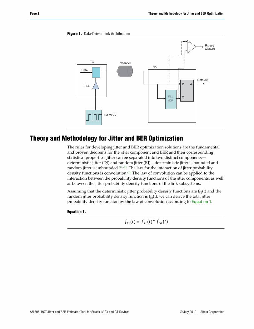
Any communication link is composed of three key subsystems—the transmitter (TX), receiver (RX), and channel (CH) in between them. Commonly used at multiple Gbps data rates, is a data-driven architecture where the clock is recovered at the receiver from the incoming serial data bit stream. Figure 1 shows a data-driven architecture. The link is expected to satisfy the overall BER requirements set by many high-speed I/O (HSIO) standards and is typically at 10-12 or lower.
AN 608: HST Jitter and BER Estimator Tool for Stratix IV GX and GT Devices
Page 2 Theory and Methodology for Jitter and BER Optimization
Theory and Methodology for Jitter and BER OptimizationThe rules for developing jitter and BER optimization solutions are the fundamental and proven theorems for the jitter component and BER and their corresponding statistical properties. Jitter can be separated into two distinct components—deterministic jitter (DJ) and random jitter (RJ)—deterministic jitter is bounded and random jitter is unbounded (1) , (2). The law for the interaction of jitter probability density functions is convolution (2). The law of convolution can be applied to the interaction between the probability density functions of the jitter components, as well as between the jitter probability density functions of the link subsystems.
Assuming that the deterministic jitter probability density functions are fDJ(t) and the random jitter probability density function is fRJ(t), we can derive the total jitter probability density function by the law of convolution according to Equation 1.
Theory and Methodology for Jitter and BER Optimization Page 3
The law of convolution works well for the interaction between the jitter components. It also works well for jitter between the link subsystems of the TX, RX, and channel. Figure 2 shows the jitter interaction for the data-driven link architecture shown in Figure 1.
The first order jitter probability density function from each subsystem is independent. The overall system jitter probability density function is linked to the probability density functions of the link subsystems, as shown in Equation 2.
Equation 2 represents a different usage model for the jitter probability density function within a link system. Equation 2 can be further expanded in terms of the deterministic jitter and random jitter probability density functions of each subsystem by using Equation 1. The results are shown in Equation 3.
Because the order of convolution is interchangeable, you can rewrite and regroup Equation 3 to that shown in Equation 4.
Figure 2. Jitter Probability Density Functions for the TX, RX, and Channel Link Subsystems
Page 4 Theory and Methodology for Jitter and BER Optimization
1 Because the channel is a passive medium, the channel only contains deterministic jitter.
Using the overall system jitter probability density function, the BER (denoted as β and caused by jitter), is estimated as shown in Equation 5.
Equation 5 implies that you can estimate the link BER given the system jitter probability density function, which depends on the probability density functions of the link subsystems of the TX, RX, and channel. The inverse is also true—given the system BER, the jitter probability density function of the system can be constrained or uniquely determined. Furthermore, the jitter probability density function of a subsystem can be constrained or uniquely determined if you know or assume the probability density functions of the other subsystems.
Random jitter is best described by a Gaussian model, while deterministic jitter is best described by the peak-to-peak value (pk-pk) if you do not know the detail of the probability density function. Using these assumptions, Equation 4 can be shown as Equation 6.
1 Jitter sources relevant to BER are those non-trackable or non-equalizable jitters. Therefore, in estimating the system jitter probability density function, you must consider the effect of equalization and clock recovery. To determine the non-equalizable link jitter, the HST jitter and BER estimator tool has an integrated link simulator for the Altera® Stratix IV GX and GT devices. The clock recovery effect on TX jitter is accommodated using measurement clock-recovery (TX Measurement CDR BW) emulation.
Theory and Methodology for Jitter and BER Optimization Page 5
HST Jitter and BER Estimator Tool ExamplesTX jitter, RX jitter, channel jitter, and/or BER are essential for quantifying link performance. You can estimate the value of any one of these characteristics if you know the values of the other three characteristics. Table 1 lists the HST jitter and BER estimator tool analysis options.
Case 1—Link BER EstimationFigure 3 shows an example for link BER estimation. If you know the subsystems’ jitter for the TX, RX, and non-equalizable channel deterministic jitter, the HST jitter and BER estimator tool calculates the link BER and provides the available TJ margin at the link target BER, and the BER at the center of the eye is estimated.
In this example, the link is operating at 6.375 Gbps with both TX and RX configured as Stratix IV GX devices (in the TX Device and RX Device options). The channel is Tyco 30" legacy backplane S-parameters. Non-equalizable channel deterministic jitter is estimated using the pre-emphasis and equalization link estimator (PELE)-based link simulator in the HST jitter and BER estimator tool with the following settings:
■ TX pre-emphasis (Pre-Emph Opt Mode) in Auto mode
■ RX CTLE Opt Mode in Auto mode (AC Gain Level is ignored)
■ RX DC Gain Level set to 0 (0 dB)
■ RX decision feedback equalization (DFE Optimization Mode) set to Disabled
Table 1. HST Jitter and BER Estimator Tool Analysis Options (Note 1)
TX CH RX BER
Case 1—Link BER Estimation v v v ?
Case 2—Maximum Allowable Channel Deterministic Jitter Estimation
v ? v v
Case 3—Allowable TX Jitter Estimation ? v v v
Case 4—Allowable RX Jitter Estimation v v ? v
Note to Table 1:
(1) v = known characteristics; ? = to be estimated from the known information.
Theory and Methodology for Jitter and BER Optimization Page 7
Case 2—Maximum Allowable Channel Deterministic Jitter EstimationFigure 4 shows an example for the maximum allowable channel deterministic jitter estimation. If you know the subsystems’ jitter for the TX and RX, the HST jitter and BER estimator tool calculates the allowable channel deterministic jitter that can be present in the system for the specified link target BER.
In this example, the link is operating at 6.375 Gbps with both TX and RX configured as Stratix IV GX devices (in the TX Device and RX Device options). Though the manually entered non-equalizable channel deterministic jitter (in the Non Equalizable Channel DJ Source option) is 0.1 UI in this example, the maximum allowable channel deterministic jitter is estimated as 0.409 UI.
Figure 4. Estimating the Maximum Allowable Non-Equalizable Channel Deterministic Jitter
Page 8 Theory and Methodology for Jitter and BER Optimization
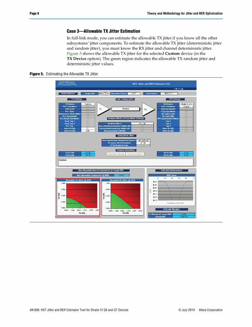
Case 3—Allowable TX Jitter EstimationIn full-link mode, you can estimate the allowable TX jitter if you know all the other subsystems’ jitter components. To estimate the allowable TX jitter (deterministic jitter and random jitter), you must know the RX jitter and channel deterministic jitter. Figure 5 shows the allowable TX jitter for the selected Custom device (in the TX Device option). The green region indicates the allowable TX random jitter and deterministic jitter values.
Theory and Methodology for Jitter and BER Optimization Page 9
Case 4—Allowable RX Jitter EstimationIn full-link mode, you can estimate the allowable RX jitter if you know all the other subsystems’ jitter components. To estimate the allowable RX jitter (deterministic jitter and random jitter), you must know the TX jitter and channel deterministic jitter. Figure 6 shows the allowable RX jitter for the selected Custom device (in the RX Device option). The green region indicates the allowable RX random jitter and deterministic jitter values.
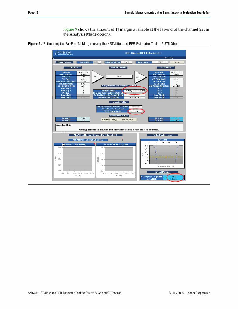
Estimating Non-Equalizable Channel Deterministic JitterNon-equalizable channel deterministic jitter is defined as channel jitter (intersymbol interference [ISI] and/or crosstalk) that can not be compensated by using TX pre-emphasis and/or RX equalizations. In full-link and far-end mode, you can select to either manually enter the non-equalizable channel deterministic jitter (in the Non Equalizable Channel DJ Source option) or use the PELE-based link simulator to estimate the non-equalizable channel deterministic jitter.
Use the channel S-parameters file in touchstone format to estimate the non-equalizable channel deterministic jitter. The channel S-parameters account for all the discontinuities due to the PCB traces, vias, connectors and/or backplanes.
Page 10 Sample Measurements Using Signal Integrity Evaluation Boards for
f For more information about the multi-path/hybrid channel S-parameters modeling and extraction, refer to AN 596: Modeling and Design considerations for 10 Gbps connectors.
Sample Measurements Using Signal Integrity Evaluation Boards for Stratix IV GX and GT Devices
The following sections describe sample measurements for Stratix IV GX and GT devices when using the signal integrity (SI) evaluation boards.
Measurement SetupStratix IV GX and GT SI evaluation boards were used to perform jitter measurements at the far-end of the link. Figure 7 shows the measurement setup.
The transceiver output is fed to the external BERTScope variable clock recovery unit (CRU) to recover the transmitted clock. These experiments used SI evaluation boards GUI designs. The CRU’s data output and clock output were fed into the BERTScope 12500A error detector circuitry’s data and clock inputs, respectively. BERTScope’s jitter peak was enabled to measure the total jitter. To generate the external clock input, an Agilent 81134A pulse generator was used.
Stratix IV GX SI Evaluation Board 33” Long Trace at 6.375 GbpsFor this experiment, the total jitter was measured at the output of a 33” long board trace (GXB2_TX7) with the channel running at 6.375 Gbps. The channel S-parameters were extracted using the board file and stack-up information in the Hyperlynx 8.0. The reference clock was set to 318.75 MHz and the Stratix IV GX SI evaluation board GUI design (gxbguictrl_top3.sof) was used.
The HST jitter and BER estimator tool link simulator was used to calculate the non-equalizable channel deterministic jitter settings (in the Non Equalizable Channel DJ Source option) and to determine the optimized TX pre-emphasis settings (in the Pre-Emph Opt Mode option).
Sample Measurements Using Signal Integrity Evaluation Boards for Stratix IV GX and GT Devices Page 13
Equation 7 on page 11 shows the HST jitter and BER estimator tool estimated total jitter at the far-end of the channel. The measured far-end total jitter of 57 ps shown in Figure 10 is within the estimated value shown in Equation 7 on page 11.
Stratix IV GT SI Evaluation Board 15” Long Trace at 10.3125 GbpsFor this experiment, the total jitter was measured using a 15” long board trace (GXB2_TX1) channel running at 10.3125 Gbps. The channel S-parameters were extracted using the board file and stack-up information in Hyperlynx 8.0. The input reference clock was set to 644.53 MHz and the Stratix IV GT SI evaluation board GUI design (sof1.sof) with an external reference clock was used.
The HST jitter and BER estimator tool link simulator was used to calculate the non-equalizable channel deterministic jitter settings (in the Non Equalizable Channel DJ Source option) and to determine the optimized TX pre-emphasis settings (in the Pre-Emph Opt Mode option).
Figure 10. Far-End TJ at 6.375 Gbps using the Stratix IV GX SI Evaluation Board with 33” Long Trace
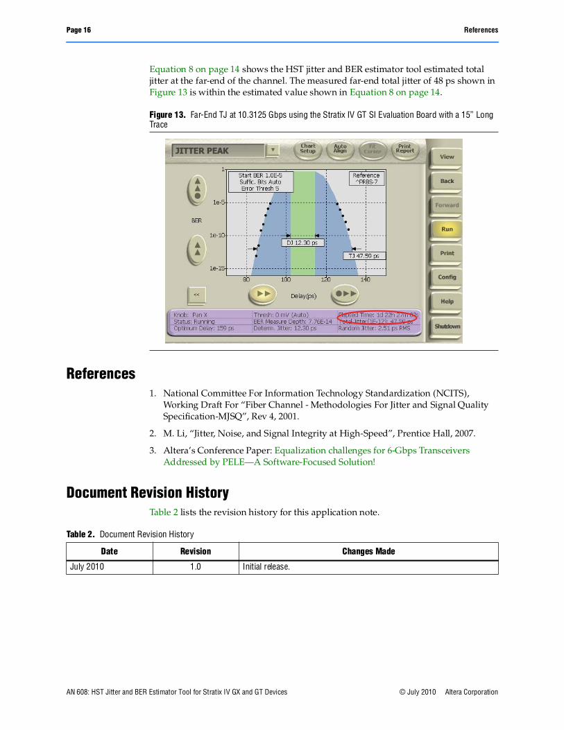
Equation 8 on page 14 shows the HST jitter and BER estimator tool estimated total jitter at the far-end of the channel. The measured far-end total jitter of 48 ps shown in Figure 13 is within the estimated value shown in Equation 8 on page 14.
References1. National Committee For Information Technology Standardization (NCITS),
Working Draft For “Fiber Channel - Methodologies For Jitter and Signal Quality Specification-MJSQ”, Rev 4, 2001.
2. M. Li, “Jitter, Noise, and Signal Integrity at High-Speed”, Prentice Hall, 2007.
3. Altera’s Conference Paper: Equalization challenges for 6-Gbps Transceivers Addressed by PELE—A Software-Focused Solution!
Document Revision HistoryTable 2 lists the revision history for this application note.
Figure 13. Far-End TJ at 10.3125 Gbps using the Stratix IV GT SI Evaluation Board with a 15” Long Trace