12
AN-768 2017.05.08

AN 768: Multi-Rate (Up to 12G)SDI II Reference Design for Intel®Arria® 10 DevicesAN-7682017.05.08
SubscribeSend Feedback

Contents
1 AN 768: Multi-Rate (Up to 12G) SDI II Reference Design for Intel Arria 10 Devices....... 31.1 Setting up the Hardware .........................................................................................41.2 Running the Multi Rate (Up to 12G) SDI II with External VCXO Reference Design............ 7
1.2.1 Receiver.................................................................................................... 81.2.2 Parallel Loopback........................................................................................8
1.3 Reference Design Components................................................................................. 91.3.1 Channel Data Rate.................................................................................... 10
1.4 Compiling the Design and Configuring the FPGA........................................................111.5 Document Revision History.....................................................................................12
Contents
AN 768: Multi-Rate (Up to 12G) SDI II Reference Design for Intel® Arria® 10 Devices2
1 AN 768: Multi-Rate (Up to 12G) SDI II ReferenceDesign for Intel Arria 10 Devices
The multi rate (up to 12G) Serial Digital Interface II (SDI II) with external voltage-controlled crystal oscillator (VCXO) reference design demonstrates the transmissionand reception of video data using the Intel SDI II IP core, Intel Arria® 10 GX FPGADevelopment Kit, and the Nextera FMC daughter card.
The reference design allows single-link transmission of SDI video data at data rates upto 12 Gbps, which supports 4Kp60. This reference design supports these standards:
• SD-SDI
• HD-SDI
• 3G-SDI
• 6G-SDI
• 12G-SDI
The multi rate SDI II with external VCXO reference design consists of a simplex TXchannel and a simplex RX channel. Each channel has its own blocks to operateindependently.
• Channel 0 TX
— Transceiver Native PHY in TX Simplex mode
— SDI II transmitter instance
— TX channel Transceiver PHY reset controller
— TX PLL
• Channel 0 RX
— Transceiver Native PHY in RX Simplex mode
— SDI II IP receiver instance
— RX channel Transceiver PHY reset controller
— Transceiver reconfiguration management block
1 AN 768: Multi-Rate (Up to 12G) SDI II Reference Design for Intel Arria 10 Devices
Intel Corporation. All rights reserved. Intel, the Intel logo, Altera, Arria, Cyclone, Enpirion, MAX, Nios, Quartusand Stratix words and logos are trademarks of Intel Corporation or its subsidiaries in the U.S. and/or othercountries. Intel warrants performance of its FPGA and semiconductor products to current specifications inaccordance with Intel's standard warranty, but reserves the right to make changes to any products and servicesat any time without notice. Intel assumes no responsibility or liability arising out of the application or use of anyinformation, product, or service described herein except as expressly agreed to in writing by Intel. Intelcustomers are advised to obtain the latest version of device specifications before relying on any publishedinformation and before placing orders for products or services.*Other names and brands may be claimed as the property of others.
ISO9001:2008Registered

Figure 1. Multi Rate (Up to 12G) SDI II with External VCXO Reference Design BlockDiagram
Channel 0
VCXO(148.5/148.35 MHz)
Oscillator(100 MHz)
Arria 10 GX Device
Clock Input 297/296.7 MHzClock Input 100 MHzClock Input 148.5/148.35 MHz
Control and StatusVideo DataFeedback
TX ClockHeartbeat
RX ClockHeartbeat
LoopbackFIFO Buffer
TX Transceiver PHYReset Controller
Arria 10 Native PHYTX
TX PLL
Multi Rate SDI II IP Core (TX)
TX Top
Arria 10 Native PHY(RX)
Multi Rate SDI II IP Core (RX)
RX Top
RX TransceiverReconfiguration
Management
CDR
RX Transceiver PHYReset Controller
ALTCLKCTRL(Clock Control IP Core)
12G SDI RX(LMH 1219)
Line Lock Clock(LMH 1983)
Ultra-Low Jitter PLL(LMK 03328)
12G SDI TX(LMH 1218)
FMC Connector Port B
FMC Development Module (VIDIO-12G-A)
27 MHz
FVH Video Sync
tx_clkout
rx_clkout
reconfig_clk
BNC Connector(To SDI Signal Analyzer)
BNC Connector(From SDI Signal Generator)
User LED User LED
Serial Clock
For more information about each component in the block diagram, refer to ReferenceDesign Components on page 9.
Related Links
• Arria 10 Multi Rate (Up to 12G) SDI II with External VCXO Reference Design 16.0Provides the design files for this reference design.
• SDI II User Guide
• Arria 10 Transceiver PHY User Guide
1.1 Setting up the Hardware
Complete the steps in the following topics to set up the hardware for the multi rateSDI II with external VCXO reference design.
Hardware and Software Requirements
The multi rate SDI II with external VCXO reference design requires the followinghardware and software:
1 AN 768: Multi-Rate (Up to 12G) SDI II Reference Design for Intel Arria 10 Devices
AN 768: Multi-Rate (Up to 12G) SDI II Reference Design for Intel® Arria® 10 Devices4

• Arria 10 GX FPGA Development Board (10AX115S3F45E2SGE3)
• VIDIO™ FMC Development Module VIDIO-12G-A (Nextera FMC daughter card)
• BNC plug to BNC plug cables
• 12G SDI Signal Analyzer
• 12G SDI Signal Generator
• Quartus® Prime software version 16.0
Connecting the Hardware
Figure 2. Hardware Setup
SDI Video Ports(SDI IN (J1), SDI OUT (J2))
Push Button(PB0)
cpu_resetn (S4)
12 V DC Input Jack(J13)
On-BoardIntel FPGADownloadCable II (J3)
Nextera FMCDaughter Card
Arria 10 FPGA Development Board
Plug the Nextera FMC daughter card to the FMC connector port B. Connect thedevelopment board to 12V DC input (J13) power supply.
Setting the DIP Switches
Set the DIP switches of the development board as specified below.
Table 1. DIP Switch Control Settings
DIP Switch SchematicSignal Name
Description Setting
SW3(PCIe*)
1 X1 ON for PCIe X1 ON
2 X4 ON for PCIe X4 ON
3 X8 ON for PCIe X8 ON
4 — OFF for 1.35 V MEM_VDD power rail OFF
SW4(JTAG)
1 Arria 10 OFF to enable the Arria 10 device in the JTAG chain OFF
2 MAX V OFF to enable the MAX V device in the JTAG chain OFF
continued...
1 AN 768: Multi-Rate (Up to 12G) SDI II Reference Design for Intel Arria 10 Devices
AN 768: Multi-Rate (Up to 12G) SDI II Reference Design for Intel® Arria® 10 Devices5

DIP Switch SchematicSignal Name
Description Setting
3 FMCA ON to bypass the FMCA connector in the JTAG chain ON
4 FMCB ON to bypass the FMCB connector in the JTAG chain ON
SW5(Configuration) 1
1 MSEL0 ON for MSEL0 = 1; for FPP standard mode OFF
2 MSEL1 ON for MSEL1 = 0; for FPP standard mode OFF
3 MSEL2 ON for MSEL2 = 0; for FPP standard mode ON
4 VIDEN OFF for enabling VID_EN for the Smart Voltage ID(SmartVID) feature
ON
SW6(Board Settings)
1 CLK_SEL ON for 100 MHz on-board clock oscillator selectionOFF for SMA input clock selection
ON
2 CLK_EN OFF for setting CLK_ENABLE signal high to the MAX Vdevice
OFF
3 Si516_FS ON for setting the SDI REFCLK frequency to 148.35MHzOFF for setting the SDI REFCLK frequency to 148.5MHz
OFF
4 FACTORY ON to load factory image from flashOFF to load user hardware from flash
ON
5 RZQ_B2K ON for setting RZQ resistor of Bank 2K to 99.17 ohmOFF for setting RZQ resistor of Bank 2K to 240 ohm
OFF
Figure 3. DIP Switches
On
Off1 2 3 4
SW3On
Off1 2 3 4
SW4On
Off1 2 3 4
SW5On
Off1 2 3 4
SW6
5
Jumper Settings
Figure 4. Jumper Settings on the Nextera FMC Daughter Card
Pin 2 - 3296.7 MHz
OpenPin 1 - 2SDI Mode
1 Set the MSEL [2:0] bits according to your chosen configuration scheme.
1 AN 768: Multi-Rate (Up to 12G) SDI II Reference Design for Intel Arria 10 Devices
AN 768: Multi-Rate (Up to 12G) SDI II Reference Design for Intel® Arria® 10 Devices6

Note: Refer to the jumper settings to change the jumper (J8) position before you switchbetween PAL and NTSC video format. You must press the push button (PB0) to triggera device (LMK03328) power cycling through the PDN pin every time you change thejumper (J8) position.
Table 2. Jumper SettingsSet the jumper position of the Nextera daughter card as specified below.
Jumper Block Description Setting
J7 Programming header.
J8 To switch frequency between PAL and NTSC for TX channel.• Pin 1–2 = 297 MHz• Pin 2–3 = 297/1.001 MHz
• 1–2 for PAL• 2–3 for NTSC
J9 To select SDI or IP mode. Pin 1-2 =SDI Mode; pin 2-3=IPmode• Pin 1–2 = SDI Mode• Pin 2–3 = IP mode
1–2
Port Assignments
Table 3. SDI Channels and PortsFPGA pins and physical ports for SDI TX/RX channels
Transceiver Channel FPGA Pin Physical Port onNextera Daughter Card
Channel 0 TX AB1/AB2 SDI_OUT (J2)
Channel 0 RX Y5/Y6 SDI_IN (J1)
Clock Input
Table 4. Input Clock Frequency and FPGA PinsInput clock frequency and FPGA pins for the multi rate SDI II reference design.
Hardware Input ClockFrequency
FPGA Input Pin Description
Arria 10 GX development board 100 MHz F23/G23 As the channel 0 reconfig clock
Arria 10 GX development board 148.5/148.35 MHz L37/L38 As the reference clock for channel 0rx_coreclk and rx_cdr_refclk0, and RX PHYreset controller.
Nextera FMC daughter card 297/296.7 MHz W8/W7 As the reference clock for channel 0 fPLL,and TX PHY reset controller
1.2 Running the Multi Rate (Up to 12G) SDI II with External VCXOReference Design
When the board is set up and the FPGA is configured, you can start running thedemonstration tests. Subsequent topics describe the tests that you can run.
Table 5. User LEDsThe User LEDs indicate the expected results. A logical 1 indicates that the LED illuminates, a logical 0 indicatesotherwise.
1 AN 768: Multi-Rate (Up to 12G) SDI II Reference Design for Intel Arria 10 Devices
AN 768: Multi-Rate (Up to 12G) SDI II Reference Design for Intel® Arria® 10 Devices7

User LEDs Description
D3 The heartbeat of the transmitter clock out for channel 0.
D4 The heartbeat of the receiver recovered clock out for channel 0.
D5 Frame locked for channel 0.
D6 TRS locked for channel 0.
D7 CRC error on Chroma/Luma for channel 0.Applicable for all modes except SD-SDI.
D8–D10 RX signal standard for channel 0:• SD: [D8, D9, D10] = 000• HD: [D8, D9, D10] = 001• 3Gb: [D8, D9, D10] = 010• 3Ga: [D8, D9, D10] = 011• 6Gb: [D8, D9, D10] = 100• 6Ga: [D8, D9, D10] = 101• 12Gb: [D8, D9, D10] = 110• 12Ga: [D8, D9, D10] = 111
Note: You need to compile and configure the design before you run the tests. For moreinformation about compiling and configuring the design, refer to Compiling the Designand Configuring the FPGA on page 11.
Reset
You may reset the reference design by pressing the S4 push button on thedevelopment board.
1.2.1 Receiver
To run the test, connect an SDI signal generator to the receiver input, SDI_IN (J1),of channel 0.
This test uses the following user LEDs to indicate the respective conditions:
• D8, D9, and D10 indicate the receiver signal standard.
• D7 illuminates when the CRC error signal for channel 0 is asserted.
• D6 illuminates when the trs_locked signal for channel 0 is asserted.
• D5 illuminates when the frame_locked signal for channel 0 is asserted.
Figure 5. User LEDs
D3 D4 D5 D6 D7 D8 D9 D10
Arria 10 GX Development Kit User LEDs
1.2.2 Parallel Loopback
Follow these steps to run the parallel loopback test:
1 AN 768: Multi-Rate (Up to 12G) SDI II Reference Design for Intel Arria 10 Devices
AN 768: Multi-Rate (Up to 12G) SDI II Reference Design for Intel® Arria® 10 Devices8

1. Connect an SDI signal generator to the receiver input, SDI_IN (J1), of channel 0.
2. Connect an SDI signal analyzer to the transmitter output, SDI_OUT (J2), ofchannel 0.
3. Check the result on the SDI signal analyzer.
This test uses the following user LEDs to indicate the respective conditions:
• D8, D9, and D10 indicate the receiver signal standard.
• D7 illuminates when the CRC error signal for channel 0 is asserted.
• D6 illuminates when the trs_locked signal for channel 0 is asserted.
• D5 illuminates when the frame_locked signal for channel 0 is asserted.
Figure 6. User LEDs
D3 D4 D5 D6 D7 D8 D9 D10
Arria 10 GX Development Kit User LEDs
Note: LMH1983 does not support 1080 p48 format. For more details, refer to the TexasInstrument LMH1983 Datasheet.
1.3 Reference Design Components
The following table describes each component for the multi rate SDI II with externalVCXO reference design.
Table 6. Design Components Specific to Multi Rate SDI II with External VCXOReference Design
TX/RX Multi Rate SDI II IP Core The SDI II IP core.Channel 0 TX/RX—the instance of the SDI II IP in this channel isconfigured in simplex TX/RX mode to support SD-SDI, HD-SDI, 3G-SDI, 6G-SDI, and 12G-SDI.Channel 0 of the SDI RX receives external SDI video data from theBNC port through the transceiver RX pin.For more information, refer to Channel Data Rate on page 10.
TX PLL The Arria 10 fPLL IP core. This reference design uses an fPLL core asthe TX PLL for the Arria 10 Transceiver Native PHY IP.This IP core uses 297/296.7 MHz frequency derived from the NexteraFMC daughter card as a reference clock.
TX/RX Arria 10 Transceiver Native PHY The Altera Arria 10 Transceiver Native PHY IP core. The referencedesign uses this PHY IP to configure the transceiver PHY for the SDI IIprotocol implementation. You can select the preset settings for the PHYIP core defined for the SDI II protocol. To apply a preset to the PHY IPcore, double click the preset name. When you apply a preset, the PHYparameters are set accordingly for the instance.For example:
continued...
1 AN 768: Multi-Rate (Up to 12G) SDI II Reference Design for Intel Arria 10 Devices
AN 768: Multi-Rate (Up to 12G) SDI II Reference Design for Intel® Arria® 10 Devices9
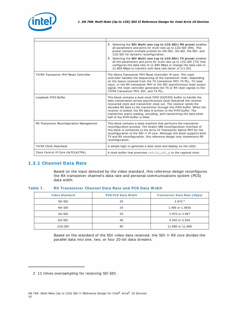
• Selecting the SDI Multi rate (up to 12G-SDI) RX preset enablesall parameters and ports for multi rate up to 12G-SDI (RX). Thispreset contains multiple profiles for HD-SDI, 3G-SDI, 6G-SDI, and12G-SDI for dynamic reconfiguration.
• Selecting the SDI Multi rate (up to 12G-SDI) TX preset enablesall the parameters and ports for multi rate up to 12G-SDI (TX) thatconfigures the data rate of 11,880 Mbps or change the data rate to11,868 Mbps to transmit with data rate factor of 1/1.001
TX/RX Transceiver PHY Reset Controller The Altera Transceiver PHY Reset Controller IP core. This resetcontroller handles the sequencing of the transceiver reset. Dependingon the status received from the TX transceiver PHY, TX PLL, TX resetinput, or the RX transceiver PHY or the SDI asynchronous reset outputsignal, the reset controller generates the TX or RX reset signals to theTX/RX transceiver PHY, SDI, and TX PLL.
Loopback FIFO Buffer This block contains a dual-clock FIFO (DCFIFO) buffer to handle thedata transmission across asynchronous clock domains—the receiverrecovered clock and transmitter clock out. The receiver sends thedecoded RX data to the transmitter through this FIFO buffer. When thereceiver is locked, the RX data is written to the FIFO buffer. Thetransmitter starts reading, encoding, and transmitting the data whenhalf of the FIFO buffer is filled.
RX Transceiver Reconfiguration Management This block contains a state machine that performs the transceiverreconfiguration process. The Avalon-MM reconfiguration interface ofthis block is connected to the Arria 10 Transceiver Native PHY for thereconfiguration of the SDI II IP core. Although this block supports bothTX and RX reconfiguration, this reference design only implements RXreconfiguration.
TX/RX Clock Heartbeat A simple logic to generate a slow clock and display on the LEDs.
Clock Control IP Core (ALTCLKCTRL) A clock buffer that promotes refclk_sdi_p to the regional clock.
1.3.1 Channel Data Rate
Based on the input detected by the video standard, this reference design reconfiguresthe RX transceiver channel's data rate and personal communications system (PCS)data width.
Table 7. RX Transceiver Channel Data Rate and PCS Data Width
Video Standard PCS-PLD Data Width Transceiver Data Rate (Gbps)
SD-SDI 20 2.970 2
HD-SDI 20 1.485 or 1.4835
3G-SDI 20 2.970 or 2.967
6G-SDI 40 5.940 or 5.934
12G-SDI 80 11.880 or 11.868
Based on the standard of the SDI video data received, the SDI II RX core divides theparallel data into one, two, or four 20-bit data streams.
2 11 times oversampling for receiving SD-SDI.
1 AN 768: Multi-Rate (Up to 12G) SDI II Reference Design for Intel Arria 10 Devices
AN 768: Multi-Rate (Up to 12G) SDI II Reference Design for Intel® Arria® 10 Devices10

Table 8. Data Streams for Different Video Standards
Video Standards Data Stream
SD-SDI, HD-SDI, 3G-SDI 1
6G-SDI 2
12G-SDI 4
In this reference design, the video data from Channel 0 RX —in four 20-bit datastreams —are looped back internally to Channel 0 TX for retransmission.. This channeldemonstrates a receiver-to-transmitter loopback by decoding, buffering, andretransmitting the received video data to be displayed on the scope. The SDI II RXcore uses an external clock of 148.5 or 148.35 MHz.
Related Links
TX SampleProvides more information about TX oversampling.
1.4 Compiling the Design and Configuring the FPGA
You must compile the design before you can configure the FPGA. Because the designis volatile, you must reload the design each time you power on the board.
Follow these steps to compile the design and configure the Arria 10 device:
1. To test the reference designs targeted on Arria 10 device, download the referencedesign file to your local project directory:
Arria 10 Multi Rate (Up to 12G) SDI II with External VCXO Reference Design:sdi_mr_a10_vcxo_an768.par
2. Launch the Quartus Prime software.
3. On the File menu, click New Project Wizard.
4. On the New Project Wizard page, open Design Template Installation. Selectthe design template you want to install. Click Next, then Finish.
5. On the Processing menu, click Start Compilation.
6. Before you begin the FPGA configuration, ensure that the Quartus PrimeProgrammer and the Intel® FPGA Download Cable II driver are installed on thehost computer, the board is powered, and no other applications that use the JTAGchain are running.
7. Connect the USB cable to the board.
8. On the Tools menu, click Programmer.
9. Click Auto Detect to display the devices in the JTAG chain and select a device.
10. Right click and select Change File. Then, select the appropriate .sof file fromthe project directory and click Open.
11. Turn on the Program/Configure option for the .sof file.
12. Click Start to download the .sof file to the FPGA. Configuration is complete whenthe progress bar reaches 100%.
1 AN 768: Multi-Rate (Up to 12G) SDI II Reference Design for Intel Arria 10 Devices
AN 768: Multi-Rate (Up to 12G) SDI II Reference Design for Intel® Arria® 10 Devices11

1.5 Document Revision History
The table shows the revision history for this application note.
Table 9. Document Revision History
Date Version Changes
May 2017 2017.05.08 Rebranded as Intel.
June 2016 2016.06.03 Initial release.
1 AN 768: Multi-Rate (Up to 12G) SDI II Reference Design for Intel Arria 10 Devices
AN 768: Multi-Rate (Up to 12G) SDI II Reference Design for Intel® Arria® 10 Devices12


