An effective way to simultaneous realization ofexcellent optical and electrical performance in large-scale Si nano/microstructuresZengguang Huang1,2, Sihua Zhong1, Xia Hua1, Xingxing Lin1, Xiangyang Kong3, Ning Dai4
and Wenzhong Shen1*1 Laboratory of Condensed Matter Spectroscopy and Opto-Electronic Physics, and Key Laboratory of Artificial Structures and QuantumControl (Ministry of Education), Department of Physics, and Institute of Solar Energy, Shanghai Jiao TongUniversity, Shanghai 200240, China2 School of Science, Huaihai Institute of Technology, Lianyungang 222005, Jiangsu Province, China3 School of Materials Science and Engineering, Shanghai Jiao Tong University, Shanghai 200240, China4 National Laboratory for Infrared Physics, Shanghai Institute of Technical Physics, Chinese Academy of Sciences, Shanghai 200083, China
silicon nanowires; large scale; atomic layer deposition; Al2O3; field effect passivation; minority carrier lifetime
*Correspondence
Wenzhong Shen, Laboratory of Condensed Matter Spectroscopy and Opto-Electronic Physics, and Key Laboratory of Artificial Struc-tures and Quantum Control (Ministry of Education), Department of Physics, and Institute of Solar Energy, Shanghai Jiao Tong Univer-sity, Shanghai 200240, China.E-mail: [email protected]
Received 3 December 2013; Revised 5 March 2014; Accepted 25 March 2014
1. INTRODUCTION
Over the past few years, vertically aligned silicon nanowirearrays (SiNWs) have attracted substantial interests, becauseof the ultralow reflection over a broad range of incidentangles [1,2] and a promising application to the high-performance solar cells at low cost [3–8]. The excellentanti-reflection of SiNWs is due to the formation of the den-sity-graded layer with features smaller than the wavelength
of light or the increase of the path length for the surfacefeatures larger than the wavelength of light [9–11]. Unfortu-nately, despite the excellent optical advantages, the SiNWs-based solar cells show yet unsatisfied energy conversionefficiencies (η) because of the serious surface recombinationarising from the concomitant high surface–volume ration.Many research groups have carried out many beneficial triesto minimize the optical and electrical losses and have indeedmade great progresses in the performance of SiNWs-based
PROGRESS IN PHOTOVOLTAICS: RESEARCH AND APPLICATIONSProg. Photovolt: Res. Appl. (2014)
Published online in Wiley Online Library (wileyonlinelibrary.com). DOI: 10.1002/pip.2506
solar cells [12–25]. Oh et al. [26] have reported an 18.2%efficient nanostructure black Si solar cell through controllingthe front surface area and Auger recombination. However,the improvement of these solar cells implies a fact that thehigh η requires the short nanostructure length, because ofthe careful balance between the reflection and the photo-carrier recombination. In other words, the minimum opticaland electrical losses cannot be simultaneously achieved inthese Si-nanostructure-based solar cells.
It is well known that the surface passivation plays acrucial role in improving cell performance by reducingthe surface recombination. Thermal oxidation, carbon thinfilms, and chlorine dielectric treatments have been widelystudied in SiNWs-based solar cells [16,27,28]; however,these processes offer limited improvement because theymerely provide the chemical passivation through saturatingthe dangling bonds. Another treatment of atomic-layer-deposition (ALD)-Al2O3 thin film not only yields theexcellent chemical passivation but also results in a strongfield effect passivation because of the fixed charges carriedby the interface of Si/Al2O3, which can substantially re-duce the surface recombination velocity (SRV) [29–34].In the ALD-Al2O3-passivated n-type planar Si, Wanget al. [35] have reported a low density of the interface trapsof ~1.8 × 1011 cm�2/eV and a high fixed charge density ofapproximately �3 × 1012 cm�2, which indicate the goodchemical and field effect passivation, respectively. Saint-Cast et al. [36] achieved an η of 21.3% by applying theALD-Al2O3 thin film to the rear surface of the p-typepassivated emitter and rear cell (with the area 20× 20mm2).
In this paper, we report the realization of bothincreasing effective minority carrier lifetime and reducingreflectance with the increase of SiNWs length, whichguarantees the simultaneous achievement of the best opti-cal (the lowest solar averaged reflectance of 1.38%) andelectrical (the lowest SRV of 44.72 cm/s) performance.The success lies in a combination of the ALD-Al2O3 withthe compound Si nano/microstructures (N/M-Strus) con-sisting of nanoscale SiNWs and microscale pyramidtexture. The composite structure exhibits the stronger fieldeffect passivation for the longer and thinner SiNWs and thereduced pure-pyramid-textured surface recombination,together with a complementary anti-reflection characteris-tic of the Si N/M-Strus at the short wavelength and theALD-Al2O3 at the long wavelength. The output perfor-mance of the Al2O3-passivated Si N/M-Strus-based solarcells is simulated by PC1D software, and the highest ηreaches up to 21.04%.
2. EXPERIMENT AND STRUCTURE
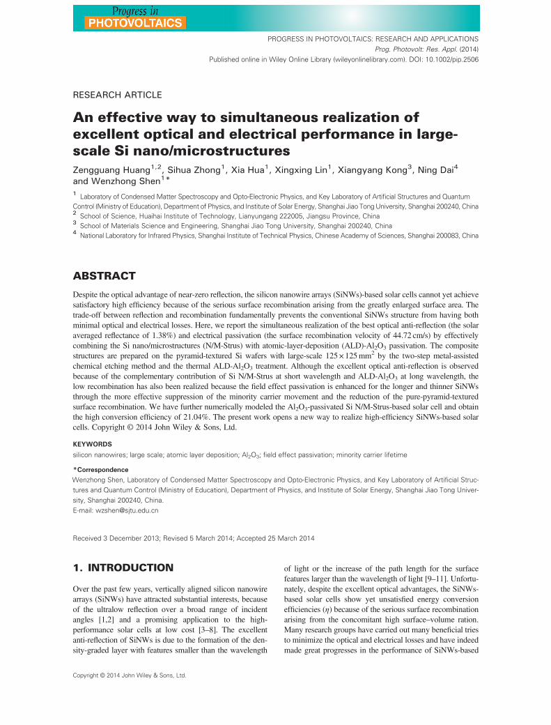
Figure 1(a) presents the main synthesis process of Al2O3-passivated Si N/M-Strus through the two-step metal-assistedchemical etching (MACE) method and ALD-Al2O3 treat-ment. First, the solar grade p-type (100) Czochralski-Si(Cz-Si) wafers (resistivity ~2Ωcm, thickness ~180μm, anda large-scale 125× 125mm2 with a pyramid texture) werecleaned in acetone and alcohol by ultrasonic washing for30min, respectively, and then immersed in 5% (volume
Figure 1. Process flow and SEM characterization of Si N/M-Strus. (a) The flow schematic diagram of the preparing process. (b) Theoblique-view SEM image of as-prepared Si N/M-Strus. Inset is the high magnitude SEM image of SiNWs on the facet of microscalepyramid texture. (c) The oblique-view SEM image of the ALD-Al2O3-coated Si N/M-Strus. Inset c1 is high magnitude SEM image of
NWs conformal coated by Al2O3 thin film. Inset c2 is the EDS of the yellow elliptical area as shown in inset c1.
Simultaneous realization of excellent optical and electrical performance Z. Huang et al.
ratio) HF for 1min to remove the natural oxide layer.Second, the Si N/M-Strus were fabricated on these wafersby the two-step MACE method [13] as follows: in the firststep, the assisted Ag+ particle clusters were deposited ontothe sample surface by immersing the cleaned wafers in the5M HF/0.02M AgNO3 fixed solution for 90 s; in the secondstep, the as-deposited samples with Ag+ particle clusterswere etched in the 5M HF/0.01M H2O2 fixed solution for100–600 s to form the SiNWs with different lengths. Afterthe MACE treatment, the residual impurities were wipedoff from the surface of SiNWs by immersing the samplesin 1:1 HNO3/H2O (volume ratio) solution for 30min atroom temperature, followed by rinsing with excess copiousdeionized water. Subsequently, the different thickness Al2O3
thin films were deposited on the surface of the as-preparedN/M-Strus samples through the reaction of trimethyla-luminum and ozone at 185 °C and 3mbar using the thermalALD method (TFS 200, Beneq, Finland). Finally, all sampleswere annealed in the atmosphere ambient at 425 °C for 5min[37] (Thermolyne, Thermo Scientific, Waltham, MA, USA),in order to activate the optimal passivation effect ofALD-Al2O3.
The morphologies of the Si N/M-Strus and elementdistribution were investigated by field emission scanningelectron microscopy (SEM, FEI Sirion 200) and the energydispersive X-ray spectroscopy (EDS). The optical reflectancespectra were obtained on the station of quantum efficiencymeasurement (QEX10, PV Measurements, Boulder, Co,USA). The effective minority carrier lifetimes were mea-sured by using the mapping mode of microwave photo-conductance method with a 904 nm wavelength laser andan average injection concentration Δn=4.81 × 1014 cm�3
(WT-2000, Semilab, Billerica, MA, USA).We divided the samples into four series (A, B, C, and
D) corresponding to the different etching times 100, 250,400, and 600 s, respectively, which yielded the SiNWslength ~180, 550, 870, and 1200 nm. Among each series,we used the number of ALD cycles, that is, 100, 250,400, 500, and 700, to characterize the different Al2O3
thickness on the Si N/M-Strus (note that one ALD cyclecan form ~0.1-nm-thick Al2O3 evaluated from the self-limiting reaction characteristics of ALD method). Hence,we could denote a sample of a certain series by combinga capital letter with the number of ALD cycles, for exam-ple, D-250 means series D (SiNWs length ~1200 nm) with250 ALD cycles (Al2O3 thickness ~25 nm).
Figure 1(b) illustrates the oblique-view SEM image ofthe Si N/M-Strus for series B consisting of the nanoscaleSiNWs along <100> crystal axis [38] and microscalepyramid texture whose facets normal is along <111>oriented direction, and the inset is the corresponding highmagnitude cross-sectional imagine of SiNWs. The averagelength of NWs is ~550 nm, and the diameter is in the range70–80 nm. Figure 1(c) shows an oblique-view SEM figure ofthe Al2O3-coated (400 ALD cycles) surface of SiNWs forseries A. We can find that the ALD-Al2O3 thin film(thickness ~40 nm) is homogeneous and conformal (see theinset c1), which benefits from the self-limiting gas–solid
reaction between the precursors and substrate. We alsogive out the EDS result of the yellow area in inset c1(see inset c2), indicating that the atom percent content ofoxygen, aluminum, and Si are 67.65%, 10.61%, and21.74%, respectively.
3. ANTI-REFLECTIONPERFORMANCE
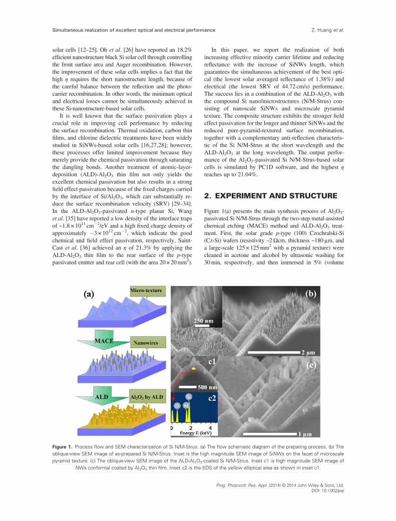
Figure 2(a) shows the experimentally obtained reflectanceRave of the naked N/M-Strus under different etching times(i.e., A-0, B-0, C-0, and D-0). Note that the solar averagedreflectance Rave here is calculated by averaging the reflec-tance over the AM1.5 spectrum in the wavelength range300–1100 nm as follows:
Rave ¼ ∫1100 nm
300 nm R λð Þ�S λð Þ�dλ
∫1100 nm
300 nm S λð Þ�dλ(1)
where R(λ) and S(λ) denote the measured reflectance andAM1.5 solar photon spectral distribution, respectively.The SiNWs lengths obtained from SEM images are alsoindicated, which show an approximate linear increasewith the etching time. We can see that the Rave of thesenaked N/M-Strus illustrates a contrary trend comparedwith the SiNWs length, implying that longer SiNWsclearly offer better light trapping effect, which matcheswell with the results in the literature [38]. Figure 2(b)further presents the reflectance spectra of the four seriesand the pure-pyramid-textured sample. Obviously, thereflectance is greatly suppressed through the entire spectracompared with that of the pyramid-textured surface, andthe anti-reflection performance is even better for longerSiNWs. Actually, the reflectance in short wavelength range300–600 nm shows much more significant improvementthan that in long wavelength 900–1100 nm, which can beattributed to the fact that the sizes of the SiNWs are com-parable with the short wavelengths [25].
Next, we turn to illustrate the anti-reflection effectof the Al2O3-coated Si N/M-Strus through the reflectancespectra of series D with different ALD cycles asshown in Figure 2(c). The solar averaged reflectance Rave
of D-0, D-250, D-400, and D-500 are calculated as6.49%, 2.63%, 1.74%, and 1.94%, respectively, presentingthat D-400 owns the best anti-reflection performance. Itshould be noted that for the long wavelength (>600 nm),the reflectance of D-250, D-400, and D-500 are greatlyreduced compared with the D-0. This is very importantbecause the excellent anti-reflection behavior of theALD-Al2O3 thin film can complement the drawback ofthe naked SiNWs in the long wavelength range. As aresult, combining the SiNWs with the ALD-Al2O3 thinfilm may be a promising design to realize excellent lighttrapping because of the anti-reflection effect both for shortand long wavelength region.
Simultaneous realization of excellent optical and electrical performanceZ. Huang et al.
We further apply the best 400 ALD cycles asdiscussed earlier to all four series (i.e., A-400, B-400,C-400, and D-400) and present the reflectance spectra inFigure 2(d). We can find that all series exhibit a substan-tial decline of the reflectance compared with the SiNWswithout coating (Figure 2(b)), and the descending trendwith the increment of SiNWs lengths is very similar aswell. Among the four series, the D-400 possesses anultralow solar averaged reflectance of 1.38% in the mostimportant wavelength region 300–900 nm where c-Sisolar cells work effectively, which is mainly distributedto the ultralow solar averaged reflectance of 1.64% inthe short wavelength range 300–450 nm and 0.85% inlong wavelength range 800–900 nm. It is worth noting,comparing with the poor short-wavelength anti-reflectionof traditional c-Si solar cells, the D-400 has reducedthe absolute solar averaged reflectance by 7.86% inthe wavelength range 300–450 nm, which addresses greatpotential for advanced photovoltaic devices. Finally,we also give out in Figure 2(e) the photograph of blackD-400 and the pyramid-textured wafer for comparison(with a large-scale 125 × 125mm2).
4. FIELD EFFECT PASSIVATIONAND APPLICATION
Although the ALD-Al2O3-coated Si N/M-Strus manifest anexcellent optical performance, a low surface recombination
is also necessarily required to achieve outstanding electricalproperties [19–24] for high-efficiency Si N/M-Strus-basedphotovoltaic or photoelectric devices. Consequently, westudy the passivation effect of the ALD-Al2O3, whichindicates the ability to suppress the surface recombinationand can be characterized by the minority carrier lifetime.Generally, the effective minority carrier lifetime τeff can beexpressed as
1τeff
¼ 1τbulk
þ SFeff þ SBeffd
(2)
where τbulk is the bulk Shockley–Read–Hall lifetime,SFeff andSBeff denote the effective SRV at the front and back surfaces,respectively, and d is the wafer thickness (in our case,d=180μm). To investigate the effect of the high surface areaon theSFeff of Si nanostructure, an expression for the measuredτeff is proposed [26] as
1τeff
¼ 1τbulk
þ AF
A�SFloc�
1dþ SBeff
d(3)
where SFloc� AF=A� �
=SFloc�α=SFeff. Here, SFloc denotes the localeffective SRV at and very near the actual front surface ofSi nanostructure, and α=AF/A is the surface area enhance-ment factor with AF being the N/M-Strus front surface areaincluding both the total lateral area of SiNWs and the pure-pyramid-textured surface area A. By using the length,
Figure 2. (a) SiNWs length (right) and the solar averaged reflectance Rave (left) of naked Si N/M-Strus with respect to etching time. (b)Reflectance spectra of series A (olive), B (magenta), C (blue), D (red), and pyramid-textured sample (black). (c) Reflectance spectraof D-0 (olive), D-250 (blue), D-400 (red), and D-500 (violet). (d) Reflectance spectra of A-400 (magenta), B-400 (olive), C-400 (blue),
and D-400 (red). (e) Photograph of D-400 and pyramid-textured wafer.
Simultaneous realization of excellent optical and electrical performance Z. Huang et al.
diameter, and the areal density of SiNWs obtained from theSEM images, α of series A, B, C, and D can be evaluatedas 2.25, 4.31, 5.86, and 7.17, respectively. Figure 3(a) showsthat α keeps approximately proportional to the SiNWs length(right) and the unpassivated Si N/M-Strus with the larger αhas the lower τave (the average value of τeff in mapping area,left), suggesting a more serious surface recombination,which matches well with our previous work [24].
Figure 3(b) demonstrates a systematic study on the τaveof all series with different ALD cycles, under the case ofone-side passivation. We can clearly find that the τaveof all passivated series greatly increase by at least oneorder of magnitude compared with the correspondingunpassivated counterparts (0 ALD cycles). Besides, theτave shows a fluctuating trend with increasing ALD cyclesand reaches the best τave at 400 ALD cycles for all fourseries, among which the D-400 has the highest value of33.23μs. When the ALD cycles become 700, the τave ofall series is observed to substantially reduce becauseof the blistering effect in an excess thick ALD-Al2O3
layer [39]. Moreover, it is of great significance that the τaveexhibits a notable increment with the increase of α(corresponding to the increasing SiNWs length less than1200 nm) for the fixed ALD cycles 100, 250, or 400(framed by the dashed-line ellipse), which is a very novelelectrical characteristic and acts totally contrary to theregular SiNWs [25,26]. This unique new finding indicatesthat the longer SiNWs (less than 1200 nm) can support
lower surface recombination, opening a new way to simul-taneously realize both the minimal optical and electricallosses [22–26].
In order to quantify the low surface recombinationbrought by the novel electrical characteristic, we alsoexplore the minority carrier lifetimes of the both-sidepassivated series (SFeff ¼ SBeff ) in Figure 3(c) with the same400 ALD cycles. The τave of the both-side passivated seriesarises along with the increase of α, which is consistentwith the one-side passivated case shown in Figure 3(b).The D-400 yields the highest τave of 55.90μs, whereasthe τmax (the maximum value of τeff in mapping area) ofthe D-400 even reaches up to 85.94μs. According toEquation (3), the SRVs corresponding to the τmax of theboth-side passivated series are calculated to be 236.63,118.43, 81.35, and 44.72 cm/s, respectively, as shown inFigure 3(d) (τbulk = 150.0μs for our low-quality solar gradep-type Cz-Si wafer with thickness ~180μm). We can seethat the SRVs of these series decline with the increase ofα, while the D-400 achieves the best SRV of 44.72 cm/s,which is extremely low benefiting from the largest τeffunder longest SiNWs. With the help of the Coronacharge–voltage property (from Semilab PV-2000), weobtain the flat band voltage of 2.153V for the optimalALD-Al2O3-passivated Si N/M-Strus (D-400). Accordingto the relationship between the fixed charge density andthe flat band voltage in the oxide/semiconductorstructure [40], the fixed charge density in the combined
Figure 3. (a) SiNWs length (red) and τave (olive) of unpassivated N/M-Strus with respect to surface area enhancement factor α. (b) Theeffect of different ALD cycles on the average τeff for series A (olive), B (red), C (green), and D (blue). (c) Column diagram of τmax (green)and τave (red) with respect to α (all series with the same 400 ALD cycles). (d) The SRV (corresponding to τmax) with respect to α (four
series with the same 400 ALD cycles).
Simultaneous realization of excellent optical and electrical performanceZ. Huang et al.
structure can be calculated to be �3.09 × 1012 cm�2, whichindicates a strong field effect passivation and is fully con-sistent with the references [35,41].
In order to provide an insight into the relationshipbetween the field effect passivation and the novelcharacteristic (the longer and thinner SiNWs possess thelower SRV), we have further studied the influence of themorphologic variation of the Si N/M-Strus on the fieldeffect passivation. Figure 4(a) reveals that the surfacemorphology of the Si N/M-Strus varies with the etchingtime. The corresponding cross-sectional schematic draw-ings (series A, B, C, and D) are shown below to better under-stand this evolution. We can see that with the increase ofetching time the SiNWs will be longer and thinner, whilethe pure-pyramid-textured surfaces (framed by dashed-line
triangles) become smaller. As is discussed earlier, theALD-Al2O3 field effect passivation is determined by thefixed charges that repel the minority carriers away fromthe surface; thus, the level of the field effect passivationcan be described by the minority carrier density (MCD)in the neighborhood of the surface. Figure 4(b) presentsthe influence of SiNWs diameter on the distribution ofMCD simulated by PC1D software, which usually simu-lates the semiconductor devices by solving the quasi-one-dimensional transport equations of electrons and holes.Note that the SiNW is equivalently simulated by settingthe layer as thick as the diameter of SiNW, and theconstant fixed charge density is set as �3.09 × 1012 cm�2
for the four series with 400 ALD cycles. We see that theGaussian distribution of MCDs in Al2O3-passivated
Figure 4. (a) SEM images and the corresponding schematics with increasing etching time 100 (series A), 250 (series B), 400 (series C),and 600s (series D), together with the pure-pyramid-textured surface framed by dashed-line triangles. (b) Distribution of the MCD withrespect to the radial distance obtained by PC1D software (the fixed charge density �3.09×1012cm�2, the doping concentration of bulkSi ~1×1016cm�3). X axis “radial distance” denotes the distance from one point on SiNWs surface to another point in SiNWs along withthe radial direction (see inset). (c) Schematic of the Si N/M-Strus-based solar cell. (d) Column diagram of η for the four series Si N/M-Strus-
based solar cells and the pure-pyramid-textured counterpart by PC1D software (see the detailed parameters in Table I).
Simultaneous realization of excellent optical and electrical performance Z. Huang et al.
SiNWs with the diameter 100 nm (length ~180 nm), 76 nm(length ~550 nm), 66 nm (length ~870 nm), and 50 nm(length ~1200 nm) reaches the peak values of 2.6 × 103,1.6 × 103, 1.2 × 10³, and 0.7 × 103 cm�3 at the SiNWscenter, respectively. Clearly, the peak values of MCDsrapidly decline with the decrease of SiNWs diameter(corresponding to the increase of SiNWs length), and allthese peak values are far less than the uniform distributionof 1.04 × 104 cm�3 (the doping concentration of bulk Si~1 × 1016 cm�3) in the unpassivated SiNWs. The lowerMCD indicates that the thinner SiNWs (corresponding tolonger SiNWs) with the constant fixed charges can moreeffectively prevent the minority carriers from bulk Simoving into the SiNWs, that is, a better field effect passiv-ation for the longer and thinner SiNWs. Moreover, thepure-pyramid-textured surface area also decreases withincreasing etching time, and thus its surface recombinationlowers. As a result, the D-400 with the longest SiNWsdemonstrates the lowest SRV, because of the strongestfield effect passivation for the thinnest SiNWs and thesmallest pure-pyramid-textured surface recombination.
The novel characteristic of this composite structureprovides a feasible solution to simultaneously achieve boththe minimum optical and electrical losses, revealing greatpotential applications to the high-performance solar cells,photoelectric detectors, or other photoelectric devices.Here, we design a Si N/M-Strus-based solar cell consistingof the n-type base region, the p-type emitter, and a confor-mal Al2O3 dielectric layer (Figure 4(c)). The upperenlarged view shows the construction of Al2O3-passivatedp–n junction, especially the p-type emitter consisting ofthe whole SiNWs and the thin layer of pyramid facets.Figure 4(d) presents the output performance of the designedsolar cell simulated by the PC1D software. Although theSi N/M-Strus-based solar cell cannot be constructed fromPC1D software, we obtain the cell performance by equiva-lently simulating planar solar cells with the reflectance andthe SRV extracted from the Al2O3-passivated Si N/M-Strus.Also, the detailed input parameters are obtained from actualdata of the production line (Table I), which further guaran-tees the reliability and accuracy of the simulation. It is clearthat the η of the Si N/M-Strus-based solar cell manifests aconsiderable increment with the increasing SiNWs, and theD-400 solar cell possesses the highest η of 21.04% that has
increased by an absolute value of 1.95% more than that ofthe traditional pyramid-textured counterpart. Particularly,the D-400 solar cell yields an ultrahigh short-circuit currentdensity of 40.09mA/cm2 (short-circuit current 6.26A in125× 125mm2), an open-circuit voltage of 0.659V, and a fillfactor of 0.796.
5. CONCLUSIONS
In conclusion, the ALD-Al2O3-passivated Si N/M-Strusformed on large-scale Si wafer by the two-step MACEmethod and ALD-Al2O3 treatment have been shown tosimultaneously realize the best optical anti-reflection andelectrical passivation for SiNWs-based solar cells. We findthat not only the optical reflection can be suppressed toextremely low levels (the solar averaged reflectance of1.38%) because of the complementary contribution of SiN/M-Strus at short wavelength and ALD-Al2O3 at longwavelength but also the electrical recombination canremain at a very low level (the SRV of 44.72 cm/s)because the longer and thinner SiNWs present lowersurface recombination. This unique abnormal decreaseof surface recombination with the increasing SiNWslength can be attributed to the stronger field effect passiv-ation for the longer and thinner SiNWs and the reducedpure-pyramid-textured surface recombination and canplay a crucial role to achieve the excellent electricalproperties in addition to the ultralow reflection in SiNWs.Furthermore, we have simulated the Al2O3-passivated SiN/M-Strus-based solar cell and obtain the high conver-sion efficiency of 21.04%. This work breaks the limitsof the trade-off between optical and electrical losses inthe SiNWs and opens a potential approach to realizehigh-efficiency SiNWs-based solar cells.
ACKNOWLEDGEMENTS
This work was supported by the National Major BasicResearch Project (2012CB934302) and the Natural ScienceFoundation of China (11174202 and 61234005).
Table I. The detailed input parameters and simulation results for the Si N/M-Strus-based solar cells with the area of 125×125mm2,together with the pyramid-textured solar cell as reference.
1. Koynov S, Brandt MS, Stutzmann M. Blacknonreflecting silicon surfaces for solar cells. AppliedPhysics Letters 2006; 88: 203107-1–203107-3.
2. Branz HM, Yost VE, Ward S, Jones KM, To B,Stradins P. Nanostructured black silicon and the opti-cal reflectance of graded-density surfaces. Applied
Physics Letters 2009; 94: 231121-1–231121-3.3. Tian B, Zheng X, Kempa T, Fang Y, Yu N, Yu G,
Huang J, Lieber C. Coaxial silicon nanowires as solarcells and nanoelectronic power sources. Nature 2007;449: 885–888.
4. Hu L, Chen G. Analysis of optical absorption in siliconnanowire arrays for photovoltaic applications. NanoLetters 2007; 7: 3249–3252.
5. Kempa TJ, Tian B, Kim DR, Hu J, Zheng X, LieberCM. Single and tandem axial p-i-n nanowire photovol-taic devices. Nano Letters 2008; 8: 3456–3460.
6. Stelzner T, Pietsch M, Andra G, Falk F, Ose E,Christiansen S. Silicon nanowire-based solar cells.Nanotechnology 2008; 19: 295203-1–295203-4.
7. Yuan G, Zhao H, Liu X, Hasanali ZS, Zou Y,Levine A, Wang D. Synthesis and photoelectro-chemical study of vertically aligned silicon nanowirearrays. Angewandte Chemie International Edition
2009; 121: 9860–9864.8. Peng KQ, Lee ST. Silicon nanowires for photovoltaic
solar energy conversion. Advanced Materials 2011;23: 198–215.
9. Garnett E, Yang P. Light trapping in silicon nanowiresolar cells. Nano Letters 2010; 10: 1082–1087.
10. KelzenbergMD, Boettcher SW, Petykiewicz JA, Turner-Evans DB, Putnam MC, Warren EL, Spurgeon JM,Briggs RM, Lewis NS, Atwater HA. Enhanced absorp-tion and carrier collection in Si wire arrays for photovol-taic application. Nature Materials 2010; 9: 239–244.
11. Han SE, Chen G. Optical absorption enhancement insilicon nanohole arrays for solar photovoltaics. NanoLetters 2010; 10: 1012–1015.
12. Kayes BM, Atwater HA, Lewis NS. Comparison ofthe device physics principles of planar and radial p-njunction nanorod solar cells. Journal of Applied
Physics 2005; 97: 114302-1–114302-11.13. Peng KQ, Xu Y, Wu Y, Yan YJ, Lee ST, Zhu J.
Aligned single-crystalline Si nanowire arrays forphotovoltaic applications. Small 2005; 1: 1062–1067.
14. Fang H, Li XD, Song S, Xu Y, Zhu J. Fabricationof slantingly-aligned silicon nanowire arrays forsolar cell application. Nanotechnology 2008; 19:255703-1–255703-6.
15. Shu Q, Wei J, Wang K, Zhu H, Li Z, Jia Y, Gui X,Guo N, Li X, Ma C, Wu D. Hybrid heterojunction
and photoelectrochemistry solar cell based on siliconnanowires and double-walled carbon nanotubes. NanoLetters 2009; 9: 4338–4342.
16. Yuan HC, Yost VE, Page MR, Stradins P, Meier DL,Branz HM. Efficient black silicon solar cell with adensity-graded nanoporous surface: optical properties,performance limitations, and design rules. AppliedPhysics Letters 2009; 95: 123501-1–123501-3.
17. Naughton M, Kempa K, Ren Z, Gao Y, Rybczynski J,Argenti N, Gao W, Wang Y, Peng Y, Naughton J,McMahon G, Paudel T, Lan Y, Burns M, Shepard A,Clary M, Ballif C, Haug F, Söderström T, Cubero O,Eminian C. Efficient nanocoax-based solar cells.Physica Status Solidi (RRL) 2010; 4: 181–183.
18. Chen C, Jia R, Li HF, Meng YL, Liu XY. Electrode-contact enhancement in silicon nanowire-array-texturedsolar cells. Applied Physics Letters 2011; 98: 143108-1–143108-3.
19. Nayak BK, Iyengar VV, Gupta MC. Efficient lighttrapping in silicon solar cells by ultrafast-laser- inducedself-assembled micro/nano structures. Progress inPhotovoltaics: Research and Applications 2011; 19:631–639.
20. Toor F, Branz HM, Page MR, Jones KM, Yuan HC.Multi-scale surface texture to improve blue responseof nanoporous black silicon solar cells. Applied Phys-ics Letters 2011; 99: 103501.
21. Kumar D, Srivastava SK, Singh PK, Husain M, KumarV. Fabrication of silicon nanowire arrays based solarcell with improved performance. Solar Energy Mate-rials and Solar Cells 2011; 95: 215–218.
22. Huang BR, Yang YK, Lin TC, Yang WL. A simpleand low-cost technique for silicon nanowire arraysbased solar cells. Solar Energy Materials and SolarCells 2012; 98: 357–362.
23. Liu YP, Lai T, Li HL, Wang Y, Mei ZX, Liang HL, LiZL, Zhang FM, Wang WJ, Kuznetsov AY, Du XL.Nanostructure formation and passivation of large-areablack silicon for solar cell applications. Small 2012; 8:1392–1397.
24. LinXX,HuaX,Huang ZG, ShenWZ.Realization of highperformance silicon nanowire based solar cells with largesize. Nanotechnology 2012; 24: 235402-1–235402-8.
25. Syu HJ, Shiu SC, Hung YJ, Hsueh CC, Lin TC,Subramani T, Lee SL, Lin CF. Influences of siliconnanowire morphology on its electro-optical propertiesand applications for hybrid solar cells. Progress in
Photovoltaics: Research and Applications 2013; 21:1400–1410.
26. Oh J, Yuan HC, Branz HM. An 18.2%-efficiencyblack-silicon solar cell achieved through control ofcarrier recombination in nanostructures. Nature Nano-technology 2012; 7: 743–748.
Simultaneous realization of excellent optical and electrical performance Z. Huang et al.
27. Wang X, Peng KQ, Pan XJ, Chen X, Yang Y, Li L,Meng XM, Zhang WJ, Lee ST. High-performance sil-icon nanowire array photoelectrochemical solarcells through surface passivation and modification.Angewandte Chemie International Edition 2011; 50:9861–9865.
28. Kim JY, Kwon MK, Logeeswaran VJ, Grego S,Islam MS. Postgrowth in situ chlorine passivationfor suppressing surface-dominant transport in siliconnanowire devices. IEEE Transactions on Nanotech-nology 2012; 11: 782–787.
29. Benick J, Hoex B, Van de Sanden M, Kessels WMM,Schultz O, Glunz SW. High efficiency n-type Si solarcells on Al2O3-passviated boron emitters. AppliedPhysics Letters 2008; 92: 253504-1–253504-3.
30. Werner F, Veith B, Tiba V, Poodt P, Roozeboom F,Brendel R, Schmidt J. Very low surface recombinationvelocities on p- and n-type c-Si by ultrafast spatialatomic layer deposition of aluminum oxide. AppliedPhysics Letters 2010; 97: 162103-1–162103-3.
31. Terlinden NM, Dingemans G, Van de Sanden MCM,Kessels WMM. Role of field-effect on c-Si surfacepassivation by ultrathin (2–20 nm) atomic layerdeposited Al2O3. Applied Physics Letters 2010; 96:112101-1–112101-3.
32. Hoex B, Van de Sanden MCM, Schmidt J, Brendel R,Kessel WMM. Surface passivation of phosphorus-diffused n+-type emitters by plasma-assisted atomic-layer deposited Al2O3. Physica Status Solidi (RRL)2012; 6: 4–6.
33. Vermang B, Goverde H, Tous L, Lorenz A, Choulat P,Horzel J, John J, Poortmans J, Mertens R. Approachfor Al2O3 rear surface passivation of industrial p-typeSi PERC above 19%. Progress in Photovoltaics:Research and Applications 2012; 20: 269–273.
34. Lee H, Tachibana T, Ikeno N, Hashiguchi H, ArafuneK, Yoshida H, Satoh S, Chikyow T, Ogura A.
Interface engineering for the passivation of c-Si withO3-based atomic layer deposited Al2O3 for solarcell application. Applied Physics Letters 2012; 100:143901-1–143901-4.
35. Wang J, Mottaghian SS, Baroughi MF. Passivationproperties of atomic-layer-deposited hafnium andaluminum oxides on Si surfaces. IEEE Transactionson Electron Devices 2012; 59: 342–348.
37. Zhu LQ, Li X, Yan ZH, Zhang HL, Wan Q. Dualfunction of antireflectance and surface passivation ofatomic-layer-deposited Al2O3 films. IEEE ElectronDevice Letters 2012; 33: 1753–1755.
38. Chen C, Jia R, Yue HH, Li HF, Liu XY, Wu DQ, DingWC, Ye TC, Kasai S, Tamotsu H, Chu JH, Wang SL.Silicon nanowire-array-textured solar cells for photo-voltaic application. Journal of Applied Physics 2010;108: 094318-1–094318-5.
39. Vermang B, Goverde H, Lorenz A, Uruena A,Vereecke G, Meersschaut J, Cornagliotti E, RothschildA, John J, Poortmans J, Mertens R. On the blistering ofatomic layer deposited Al2O3 as Si surface passivation.Proceedings of the 37th IEEE Photovoltaic SpecialistsConference, 2011; 003562–003567.
40. Casey HC, Fountain GG, Alley RG, Keller BP,DenBaars SP, Low interface trap density for remoteplasma deposited SiO2 on n-type GaN. AppliedPhysics Letters 1996; 68: 1850–1852.
41. Werner F, Veith B, Zielke D, Kühnemund L,Tegenkamp C, Seibt M, Brendel R, Schmidt J.Electronic and chemical properties of the c-Si/Al2O3
interface. Journal of Applied Physics 2011; 109:113701-1–113701-6.
Simultaneous realization of excellent optical and electrical performanceZ. Huang et al.