+ All Categories
Home > Technology > An Innovative NVM technology for Sub-0.25um SOC Applications

An Innovative NVM technology for Sub-0.25um SOC Applications

Date post: 27-Jul-2015
Category:
Upload: hkiurca-hong-kong-industry-university-research-collaboration-association
View: 20 times
Download: 0 times
Share this document with a friend
Popular Tags:
24
PMC Flash Copyright © 1998 Programmable Microelectronics Corp Al Kwok ([email protected]) 1 An Innovative NVM Technology for Sub-0.25um SOC Applications Al Kwok VP, Business Development Programmable Microelectronics Corporation [email protected] Tel.: (408) 452-1888 x103 Fax: (408) 452-1989 CASPA/CIE System-on-Chip (SOC) Symposium (5/16/98)
Transcript

PMCFlash Copyright © 1998 Programmable Microelectronics CorpAl Kwok ([email protected])

1

An Innovative NVM Technology for Sub-0.25um SOC Applications

Al KwokVP, Business Development

Programmable Microelectronics Corporation

[email protected].: (408) 452-1888 x103

Fax: (408) 452-1989

CASPA/CIE System-on-Chip (SOC) Symposium (5/16/98)

PMCFlash Copyright © 1998 Programmable Microelectronics CorpAl Kwok ([email protected])

2

Contents

• Market demands & application requirements• Challenges in embedding flash• Design for an ideal embedded flash technology• PMC’s approach and solutions• Technology highlights• Comparison with other technologies• PMC status update• Summary

PMCFlash Copyright © 1998 Programmable Microelectronics CorpAl Kwok ([email protected])

3

System-On-Chip (SOC) Requirements

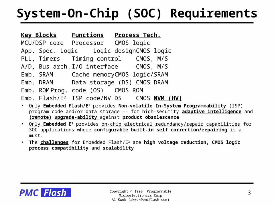
Key Blocks Functions Process Tech.MCU/DSP core Processor CMOS logicApp. Spec. Logic Logic design CMOS logic PLL, Timers Timing control CMOS, M/SA/D, Bus arch. I/O interface CMOS, M/SEmb. SRAM Cache memory CMOS logic/SRAMEmb. DRAM Data storage (DS) CMOS DRAMEmb. ROM Prog. code (OS)CMOS ROMEmb. Flash/E2 ISP code/NV DS CMOS NVM (HV)• Only Embedded Flash/E2 provides Non-volatile In-System Programmability (ISP) program

code and/or data storage -- for high-security adaptive intelligence and (remote) upgrade-ability against product obsolescence

• Only Embedded E2 provides on-chip electrical redundancy/repair capabilities for SOC applications where configurable built-in self correction/repairing is a must.

• The challenges for Embedded Flash/E2 are high voltage reduction, CMOS logic process compatibility and scalability

PMCFlash Copyright © 1998 Programmable Microelectronics CorpAl Kwok ([email protected])

4

Embedded ISP NVM Market Outlook• Semico forecasted Embedded Flash being “a sleeping giant”:

– From $836M in 1997 to $4.9B by 2001

• In-System Programmability (ISP) for high-end MCU’s:

– Over $10 billion of annual MCU sales since 1995

– On-chip Flash has higher values (as compared to ROM):• $41 for uPD70F3008Y vs. $17 for uPD703008Y• $48.5 for 68HC916Y3 vs. $25.95 for 68HC16Y3

• Smartcard IC’s incorporating Embedded EEPROM:

– Market leaders all have Embedded EEPROM features

• Embedded Flash/E2PROM for RISC, DSP, too.

• “System-on-Chip” needs Embedded Flash/EEPROM:

– ISP NVM is a must for 0.25um and beyond

– Prefer both emb. Flash & EEPROM on-chip for ease-of-use

• Applications are pervasive & virtually unlimited

• PMC has been recognized for its sub-0.3um Embedded ISP NVM solutions w/ distinct, comprehensive and solid patent portfolio

PMCFlash Copyright © 1998 Programmable Microelectronics CorpAl Kwok ([email protected])

5

Foundry Technology Trend

• Logic products/processes are preferred:– The TAM for logic products is bigger than memories– More new applications/customers, higher growth potentials– Logic products have higher GPM’s than memories

• Logic process trend is to embedded applications:– On-chip memories are imperative for high-end applications– Embedded DRAM is available now for higher integration– SOC capability w/ ISP is a must for 0.25um and beyond– Embedded Flash/E2 is imminent and will be a winning factor

• Key issues on Embedded Flash/E2:– Too few solutions for sub-0.3um CMOS logic process base-line– Need multi-generation manufacturable and scalable solution– Comprehensive IP coverage to avoid legal problems is a must!!

PMCFlash Copyright © 1998 Programmable Microelectronics CorpAl Kwok ([email protected])

6

Functions of Embedded ISP NVM

• BIOS• OS• Firmware• Boot code• Boot vector

• Data• Parametrics• Look-up table• Configurations

• Security code• Encryption• Password• Private access(Smartcard IC’s)(Electronic banking)(Internet security)

• Unlimited(user preference)(preset options)• Repair redundancy (Self-correction & repairing)

CodeStorage

DataStorage

SecurityProtection

UserProgrammables

Embedded Flash &EEPROM Functions

Flash is good for mass code and data storage with less frequent updating;EEPROM, for smaller-segment code and data storage with routine updating. For cost-effective SOC applications, both embedded Flash & EEPROM are needed.

PMCFlash Copyright © 1998 Programmable Microelectronics CorpAl Kwok ([email protected])

7

Flash Applications• Flash applications by density/power/speed requirements:

– 1M, 2M, 4M in code storage: BIOS (PC & peripherals), boot code, etc.

– 4M, 8M, 16M in code/data storage: cellular, networking, etc.

– 32M, 64M and higher in mass data storage: video/audio, SSHD w/ ECC

– 5V/12V for desk-top, equipment, etc.: where power is not an issue

– 1.8V, 2.2V, 3V for hand-held & battery-operated devices

– <1.8V for ultra-low power applications: cellular, PDA, etc.

– higher speed (</=120 ns) for machine-to-machine interface

– lower speed (>120ns) for machine-to-human interface: e.g., voice recording

• Flash technologies are application specific in nature:– NOR, stack-gate (AMD, Intel) for code & data storage in cellular, networking: high speed, high

integrity and endurance, medium densities

– NOR, other structures (Atmel, MX, ISSI, SST) for code storage in BIOS, EPROM replacements: lower density, medium/high speed

– NAND, stack-gate (Toshiba, Samsung) for data storage in digital camera, flash card, etc.: higher density, lower cost/bit w/ some error correction

– MLC, various structures (SanDisk, Intel) for mass data storage in digital camera, voice recording, SSHD: lowest speed & cost/bit w/ error correction

PMCFlash Copyright © 1998 Programmable Microelectronics CorpAl Kwok ([email protected])

8

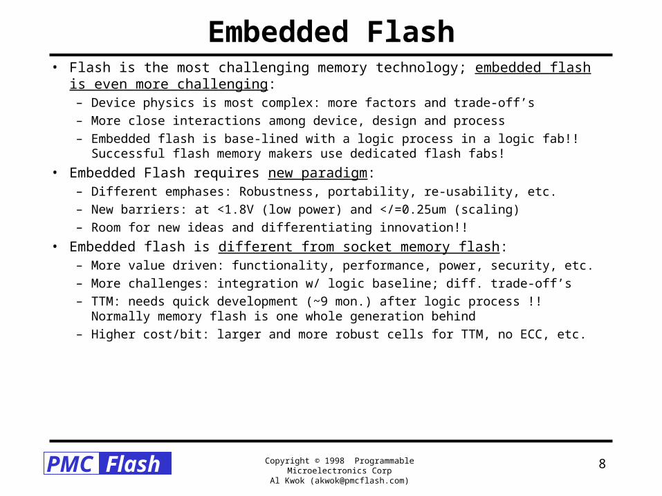
Embedded Flash• Flash is the most challenging memory technology; embedded flash is even more

challenging:– Device physics is most complex: more factors and trade-off’s – More close interactions among device, design and process– Embedded flash is base-lined with a logic process in a logic fab!! Successful flash

memory makers use dedicated flash fabs!

• Embedded Flash requires new paradigm:– Different emphases: Robustness, portability, re-usability, etc.– New barriers: at <1.8V (low power) and </=0.25um (scaling)– Room for new ideas and differentiating innovation!!

• Embedded flash is different from socket memory flash:– More value driven: functionality, performance, power, security, etc.– More challenges: integration w/ logic baseline; diff. trade-off’s– TTM: needs quick development (~9 mon.) after logic process !! Normally memory

flash is one whole generation behind– Higher cost/bit: larger and more robust cells for TTM, no ECC, etc.

PMCFlash Copyright © 1998 Programmable Microelectronics CorpAl Kwok ([email protected])

9

Wish-list for Embedded Flash• Compatibility with CMOS Logic:

– Embeddable into CMOS Logic process with minimum overhead– Little change in logic device characteristics (or SPICE models)– Little impact on design libraries (or established design investment)

• Low Vdd/power operation:– Capable of single-source 1.8V operation and below (down to 0.9V!?)– No Ids current (unlike CHE programming) -- small charge pump

• Scalable technology & competitive core size:– Lower ownership cost and quicker TTM; lower silicon cost

• Robust, IP re-usable and wide (Vtp/Vte) operating window:– Plug & play; high yield & endurance; quick time-to-market

• High endurance and reliability:– No hot hole trapping, localized stress, over-programming & over-erase

• Simple timing interface:– Deterministic (no complex algorithm); simple circuit designs; easy to use

• Granularity:– Flexible density; easy sector partition; unlimited sector size

PMCFlash Copyright © 1998 Programmable Microelectronics CorpAl Kwok ([email protected])

10

Design for an Ideal Embedded Flash• Stack-gate structure:

– Proven volume manufacturable; self-aligned & scalable– Plentiful equipment vendor support (ONO, etcher, etc.)

• Maintain ~90A to 100A tunnel oxide:– High endurance: >100K cycles

• About 50/50 divided voltage scheme:– Manage ~14V FN erase voltage req. (in <0.25um CMOS logic)

• New programming mechanisms needed:– Lower programming current than CHE; faster prog. time than FN– Lasting for multiple generations; less process sensitive– Page and byte mode programming capabilities

• FN channel erase:– Uniform field erase w/ sub. at equal potential (no current crowding)– No voltage stress on stack-gate side-wall (less process sensitive)– Proven for high endurance

PMCFlash Copyright © 1998 Programmable Microelectronics CorpAl Kwok ([email protected])

11

Design for an Ideal Flash Cell

Programming (self-regulated by lateral field cancellation):1) Float the source No Ids current (for low power)

2) Bias Drain negative Remove hot holes from the channel

3) Drain is P-type in N-well BTBT at reverse bias for electron/hole pairs

Bias N-well at Vdd (or 0V) Repel holes at sub. & stronger bias for BTBT

4) Bias CG positive Pump electrons up to FG (floating gate)

Self-regulated programming No current crowding & over-programming

Erase (w/ uniform field to the N-well of the selected sector):

1) FN channel erase Avoid side-wall process sensitivity

Result: P-channel stack-gate with BTBT prog. & FN channel erase!!

(4) + bias @ CG

P-Sub

(1) F @ S (2) - bias @ D

P+(3) N-well @ Vdd

N+e-

h+

N+

PMCFlash Copyright © 1998 Programmable Microelectronics CorpAl Kwok ([email protected])

12

Single-poly Embedded Flash

Converting stack-gate into single-poly structure (sharing the same array architecture and circuitry -- design IP reuse):

P/W

N+ (CG)

N+ (FG)

N-wellThis N+ (CG) node can withstand +/- 10V

P-Sub

P+

N+ (FG)

N+ (CG)

P+N-well

Double-poly

Single-poly

Channel area

PMCFlash Copyright © 1998 Programmable Microelectronics CorpAl Kwok ([email protected])

13

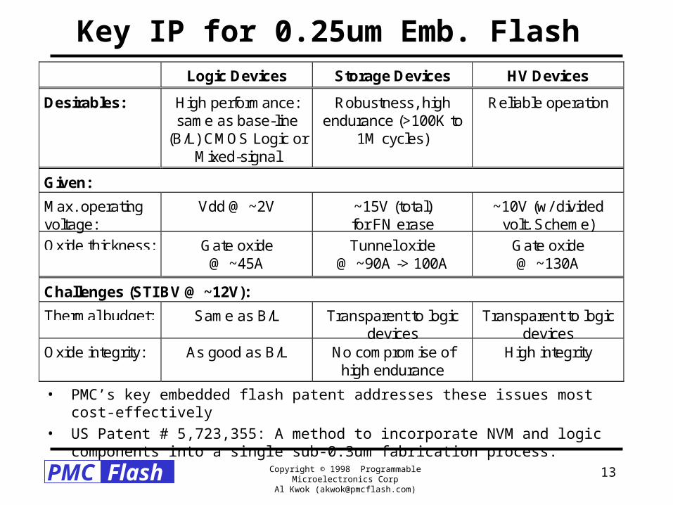
Key IP for 0.25um Emb. FlashLogic Devices Storage Devices HV Devices

Desirables: High performance:same as base-line

(B/L) CMOS Logic orMixed-signal

Robustness, highendurance (>100K to

1M cycles)

Reliable operation

Given:

Max. operatingvoltage:

Vdd @ ~2V ~15V (total)for FN erase

~10V (w/ dividedvolt. Scheme)

Oxide thickness: Gate oxide@ ~45A

Tunnel oxide@ ~90A -> 100A

Gate oxide@ ~130A

Challenges (STI BV @ ~12V):

Thermal budget: Same as B/L Transparent to logicdevices

Transparent to logicdevices

Oxide integrity: As good as B/L No compromise ofhigh endurance

High integrity

• PMC’s key embedded flash patent addresses these issues most cost-effectively• US Patent # 5,723,355: A method to incorporate NVM and logic components into

a single sub-0.3um fabrication process.

PMCFlash Copyright © 1998 Programmable Microelectronics CorpAl Kwok ([email protected])

14

SOC Challenges -- Design Aspects• 0.25um CMOS logic design/product characteristics:

– Performance: >200 MHz & higher– Data bandwidth (# of I/O): x64 or higher– Clock skew & edge rate (di/dt): Tighter and faster– Ground & Vcc bounce noise: Much worse (as %)– Vcc range (single P/S): ~2V to 1.8V– Interconnect timing budget: ~80% (dominating)– RC parasitics & spreading R: Worse (hurt flash Vt control)

• Challenges for embedding Flash/E2 core:– The on-chip high voltage (routing) must be less than 10V– Noise and disturbs are the major problems -- need isolation– Vt range is narrower for 2V Vdd -- hard to read w/o boosting & pumping

– A single-transistor cell (with sharing W/L, B/L and S/L) is not robust & manufacturable in all 0.25um SOC environments for “plug-&-play”

• Vtp and Vte window and distributions are too difficult to control

• Solution: 2-transistor cell with select gate is preferred; embedded Flash/E2 core in a separated different well

PMCFlash Copyright © 1998 Programmable Microelectronics CorpAl Kwok ([email protected])

15

PMC’s Embedded ISP NVM Options• Option 1 with P-EEPROMTM technology• Options 2 (2-T) & Option 3 (1-T) with P-FLASHTM technology

Option 1 Option 2 Option 3

Technology P-EEPROM P-FLASH P-FLASH# of poly Single Double DoubleCell type EEPROM/NOR Flash EEPROM/NOR Flash NOR Flash# of xtor/cell 2 2 1Select-gate/cell Yes Yes NoProg. / Erase states Deep depl. / Enhan. Deep depl. / Enhan. Both enhancementCell storage element Floating gate Stack-gate Stack-gateFlash cell size (um**2) 8 (0.35u), <6 (0.25u) <2.5 (0.35u), <1.35 (0.25u) ~1.2 (0.35u)E2PROM cell size (um**2) 13 (0.35u), 9 (0.25u) <8 (0.35u), <5.5 (0.25u) Not applicableProgram mechanism BTBT BTBT CHEErase mechanism FN FN FNErase window Yes (>100K cycles) No (w/ channel erase) No (w/ channel erase)Tunnel oxide (A) ~90 at window 100 100Inter-poly dielectrics N/A ONO ONOSubstrate P-sub P-sub P-subWell for cell array P-well in N-well N-well N-wellOperating voltage (LV) </= 3V </= 3V </= 3VInternal high voltage ~9V ~9V ~9V# of masking steps ~20 ~23 ~22

PMCFlash Copyright © 1998 Programmable Microelectronics CorpAl Kwok ([email protected])

16

2-T P-Flash Bias Condition2T Double Poly Flash Cell Read, Program & Erase Operation Modes:

Vdd

Vdd

1. Read Sel/Desel

0/Vdd

Vdd

1.0V

9V for 2.2<=Vdd<=3.6V

Float

2. Page/Byte Program

~ -7.5V

Vdd <=3.6V

-5.5V

-8.5V

8.5V

3. Sector Erase

8.5V

8.5V

Float

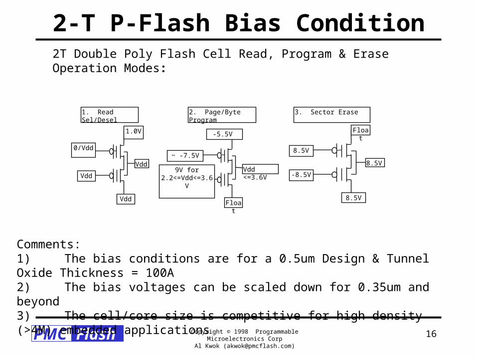
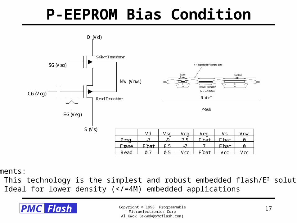
Comments:1) The bias conditions are for a 0.5um Design & Tunnel Oxide Thickness = 100A2) The bias voltages can be scaled down for 0.35um and beyond3) The cell/core size is competitive for high density (>4M) embedded applications

PMCFlash Copyright © 1998 Programmable Microelectronics CorpAl Kwok ([email protected])

17

P-EEPROM Bias Condition

S (Vs)

CG(Vcg)

EG(Veg)

SG(Vsg)

D (Vd)

NW(Vnw)

Select Transistor

Read Transistor

N+

PW

N+

PWRead Transistor

(W/L=0.8/0.6)

N+ doped poly floating gate

EraseGate

ControlGate

N-Well

P-Sub

Vd Vsg Vcg Veg Vs VnwProg. -7 -9 7.5 Float Float 0Erase Float 8.5 -7 7 Float 0Read 0.7 0.5 Vcc Float Vcc Vcc

Comments:1) This technology is the simplest and robust embedded flash/E2 solution2) Ideal for lower density (</=4M) embedded applications

PMCFlash Copyright © 1998 Programmable Microelectronics CorpAl Kwok ([email protected])

18

PMC ISP NVM Solution Overview

Emb. DRAMcompatibility

Fast page-write

Low power/Vdd

No disturb

Simpletiming interface

ComprehensiveIP Portfolio

Highendurance

Scalability w/CMOS logic

E2+Flash onsame process

PMCFlash Copyright © 1998 Programmable Microelectronics CorpAl Kwok ([email protected])

19

Key Competitive Advantages• Low power and Vdd (@ 3V and below):

– Low prog. Volt/current; low erase current; no pumping for read (for 2-T)

• Scalability w/ CMOS logic (@ 0.25um and below):– Divided/low voltage scheme; scalable cell structure; no special process

• Embedded DRAM compatibility (especially for single-poly):– Simplest in process integration; no incompatible process steps

• E2+Flash on same process flow:– Both with 2-T cells; larger cell for E2 with larger coupling capacitance

• Fast page-write (even at low Vdd):– Utilize BTBT fast programming mechanism; low prog. current

• Simple timing interface (deterministic & no wait-state):– No algorithmic Vt margin control; 2-T for E2 type timing; easily portable

• No disturb (from adjacent-cell operations or Vdd/Gnd bounces):– Robust cell margins (Vtp/Vte @ depl./enh.); 2-T with adequate cell isolation

• High endurance (and good data retention too w/ thicker tunnel oxide):– No hot-hole trapping; uniform field w/o hot spots; little DC cell currents

PMCFlash Copyright © 1998 Programmable Microelectronics CorpAl Kwok ([email protected])

20

Comparison: Device/Tech. AspectsCell Type:

Mechanism:Vendor Example:

2P/xM (2-T)BTBT/FN

PMC

ETOXCHE/FN(N-Ch.)

DINORFN/FN(N-Ch.)

Split GateCHE/FN(N-Ch.)

Sensitivity toDisturbs with scaling

Low High High High (CG & SGtied together)

Sensitivity to Over-Program or Over-erase

None High High None

Cell Current DuringWrite

< 10nA 100’s A < 1nA < 1A??

Process Complexity Medium Medium High (3P/2Mor 2P/3M)

High (non-selfaligned process)

Cell ProcessAlignm’t Sensitivity

Low Low Low High (non-self-aligned process)

Hot Hole/InterfaceDamage DuringWrite (intrinsic limitto endurance)

No Yes Yes No (but inter-polyoxide scalability

limits endur.)

Ease of ProcessIntegration withLogic

Easiest Medium (but non-symmetryjunctions)

Difficult Difficult

Compatibility with0.25µ logic process

Yes No No No

PMCFlash Copyright © 1998 Programmable Microelectronics CorpAl Kwok ([email protected])

21

Comparison: Design/Product Aspects

Cell Type:Mechanism:

Vendor Example:

2P/xM (2-T)BTBT/FN

PMC

ETOXCHE/FN(N-Ch.)

DINORFN/FN(N-Ch.)

Split GateCHE/FN(N-Ch.)

Vtp/Vte Operationmargin @ 2V

Very Wide Narrow Narrow Can be sensitiveto cycling

Disturb Concerns None Severe Severe Less

Needs EmbeddedWrite Algorithm?

No Yes Yes No

Page Mode?/SizePage Prog Time

Yes/256Bytes100s/page

No Yes/256Bytes15ms/page (1)

Yes/256Bytes5ms/page (2)

Byte Mode Prog?Byte Prog Time

Yess

Yes10s

No Yes30s (2)

MixedEEPROM/Flash?

Yes No No No

Time To Market Fast: (Less

process/designsensitive)

Slow: (Cell cannotovererase:sensitive to

process/design)

Slow: (Cell cannot

overprogram:sensitive to

process/design)

Slow: (Non-standard

process

yield/reliabilityconcerns)

Notes (1) Mitsubishi8Mb

(2) No page &byte modes in

same part

PMCFlash Copyright © 1998 Programmable Microelectronics CorpAl Kwok ([email protected])

22

Status Update• Demonstrated both 1-P & 2-P, 2-T technologies at 0.5um at TSMC:

– 1-P with outstanding product characteristics and reliability is in final qual and pilot production (silicon data to be published soon)

– 2-P with working silicon is in optimization stage

• 0.35um development in progress at another foundry

• Working with technology partners/licensees in both technologies at 0.35um and beyond

• PMC is promoting these 2 embedded flash technologies to be a de-facto standard for 0.25um SOC:– Building strategic partnership with licensees– Teaming up w/ EDA vendors for tool supports (design IP re-use)– Teaming up w/ design service partners to support licensees– Working with foundry partners to support fab-less licensees– Building strategic partnership with ASIC houses/licensees to provide system end

users one-stop service

PMCFlash Copyright © 1998 Programmable Microelectronics CorpAl Kwok ([email protected])

23

Summary• Comprehensive I.P. protection:

– 19 granted US patents & 7 granted overseas, and more pending– Over 30 US patents cover key mainstream & emerging products– NOR, NAND, MLC and embedded NVM solutions

• Scalable & robust NVM technologies:– Disturb-free and robust solutions for quick TTM– Same process for stand-alone and embedded applications– Require mainstream process modules, no special effort– Scalable to 0.18um and beyond; easier portable

• Product capability differentiation:– Low voltage/power: Easier implementation for 1.8V and lower– Faster programming capability at lower Vcc– Easier integrating Flash & full-feature E2 in the same process

• World-class partnership:– Established top-tier license partnership on </=0.25um– Key endorsements for both embedded Flash & EEPROM

PMCFlash Copyright © 1998 Programmable Microelectronics CorpAl Kwok ([email protected])

24

Technologies for Licensing

PMC offers comprehensive IP portfolio to its licensees:• For state-of-the-art embedded Flash/EEPROM applications:

– 1P/xM, 2-T, P-channel Flash/EEPROM technology:• Ideal for medium density (< 4M) embedded Flash/EEPROM core

• Most logic-like process (keep same device models & logic design library)

• Most compatible with embedded DRAM core

• Highly manufacturable and scalable; Robust and disturb-free; Valued-added features

– 2P/xM, 2-T, P-channel Flash/EEPROM technology:• Ideal for high density (>4M to 16M) embedded Flash/EEPROM core

• Highly manufacturable and scalable; robust and disturb-free; valued-added features

• For high-density Flash memory products:– 2P2M, 1-T, P-channel NOR Flash (US Pat. #5,687,118)

– P-channel Multi-Level Cell Flash (US Pat. # 5,666,307)

– P-channel NAND Flash (US Pat. # 5,581,504)


Recommended